Embed Size (px)
Citation preview
IEEE TRANSACTIONS ON ELECTRON DEVICES, VOL. 46, NO. 6, JUNE 1999 1127
Cryogenic Processed Metal–Semiconductor–Metal(MSM) Photodetectors on MBE Grown ZnSe
Hyesook Hong and Wayne A. Anderson,Senior Member, IEEE
Abstract—Molecular beam epitaxy grown 0.5-�m and 2.0-�m thick undoped ZnSe on semi-insulating (100) GaAs sub-strates were prepared for metal–semiconductor–metal (MSM)photodetector devices. The MSM photodetectors consisted ofinterdigitated metal fingers with 2, 3, and 4�m width/spacing ona wafer. A multilayer resist process was employed using polyimideand SiO2 thin films before the pattern generation to aid in a spe-cial low temperature (LT) lift-off process. Dark current–voltage(I�V ), DC photo I�V , high-frequency I�V , spectral response,and frequency response techniques were employed for testing thedevice performance. The cryogenic processed metallization pro-vided an improved interface between metal and semiconductorinterface. The breakdown voltage in these devices is dependenton the electrode width/spacing and not on film thickness. Darkcurrent remained at around 1 pA for a bias of �10 V. Thedevices exhibited a high spectral responsivity of 0.6 (A/W) at awavelength of 460 nm at 5 V applied bias. A maximum spectralresponsivity of 1 (A/W) at an applied bias of 5 V was obtainedin these devices indicating an internal gain mechanism. Thisinternal gain mechanism is attributed to hole accumulation inZnSe epilayers.
I. INTRODUCTION
W IDE bandgap compound semiconductors such as thosein the ZnSe family and GaN family are very at-
tractive materials for future electro-optic devices such asdeep ultraviolet (DUV) light sources, electro-optic displays,short distance communications, high density optical recordersand readers. This is especially true for ZnSe since it isclosely lattice matched to GaAs hence facilitating optoelec-tronic integrated circuits (OEIC) on GaAs. Of special interestare the metal–semiconductor–metal photodetectors (MSM-PD’s) since they are useful for monolithically integratedoptoelectronic receivers in free space optical interconnects dueto their easy fabrication and compatibility with planar stackedoptics and with field effect transistors (FET’s) [1], [2]. MSM-PD’s consist of a semiconductor absorbing layer between twoelectrodes deposited to form back-to-back Schottky contactson the semi-insulating substrate.
Controlling the Schottky barrier height is an importantissue in fabrication of MSM photodetectors on covalent bond-ing semiconductors. Moreover, compound semiconductors,such as GaAs, InAs, and ZnSSe , show Fermi levelpinning at the metal/semiconductor interface which limitsthe device characteristics. Previous studies [3]–[5] show thatlow temperature (LT) metallization resulted in an enhanced
Manuscript received August 26, 1998; revised December 22, 1998. Thereview of this paper was arranged by Editor P. K. Bhattacharya.
The authors are with the Department of Electrical and Computer Engineer-ing, State University of New York at Buffalo, Amherst, NY 14260 USA.
Publisher Item Identifier S 0018-9383(99)04208-2.
Schottky barrier height and reduced carrier trapping at themetal/semiconductor interface. Increasing the barrier heightleads to low dark currents which are in turn critical forimproving the minimum detectable power. Improving themetal/semiconductor interface leads to high speed devicesand improved detector sensitivity. Many MSM-PD’s in III–Vcompound semiconductors have been studied for optical com-munication at 1.3 and 1.55m [1]–[2], [6]–[8] wavelengths.These have good saturation characteristics which are attributedto narrow electrode width/spacing (submicron range), de-fined by -beam lithography, and small active area (usually
m ) achieved by reducing the contact area at themetal/semiconductor interface. In this study, by employingoptical lithography, low dark currents were obtained on LTprocessed ZnSe MSM-PD’s. Due to the lower dark currentsin these ZnSe MSM-PD’s, higher voltages can be appliedto obtain better charge collection as necessary for radiationdetector applications. This paper will present photolumines-cence (PL), the fabrication procedure for LT processed ZnSeMSM-PD’s, dark current–voltage ( ) characteristics, con-tinuous wave (CW) photocurrent–voltage characteristics, high-frequency photocurrent–voltage characteristics, frequency re-sponse, and spectral response of these devices.
II. EXPERIMENTAL
Elemental sources of Zn and Se were used for the MBEgrowth of ZnSe in a Riber MBE 32P system. The epilayergrowth of samples was monitored using 10 keV reflectionhigh-energy electron diffraction (RHEED) to optimize thegrowth conditions. The background pressure during growthwas around 10 Torr. On initiating growth, the streakyRHEED pattern of the GaAs surface changes immediatelyinto dim spots for a brief period, indicating an initial three-dimensional nucleation. The spots then elongate, and within afew minutes, the streaks are reestablished. This implies a layer-by-layer growth once a smooth surface has been established.0.5 m and 2.0 m thick undoped ZnSe epilayers were grownon semi-insulating GaAs(100) at 300C. After growth, theundoped ZnSe was cleaned in acetone, methanol, and de-ionized (DI) water, etched in HCl:DI HO (1:1) for 1 min,etched in HF:DI HO (1:1) for 1 min, rinsed in DI water, anddried with N gas.
The fabrication procedure for LT processed MSM-PD’s isdepicted in Fig. 1. Samples were placed on a spinner andcleaned with acetone followed by isopropanol at 4000 r/minfor 30 s. An adhesion promoter, Probimide QZ3289:QZ3290(1:9) was applied and allowed to sit for 10 s before spinning
0018–9383/99$10.00 1999 IEEE
1128 IEEE TRANSACTIONS ON ELECTRON DEVICES, VOL. 46, NO. 6, JUNE 1999
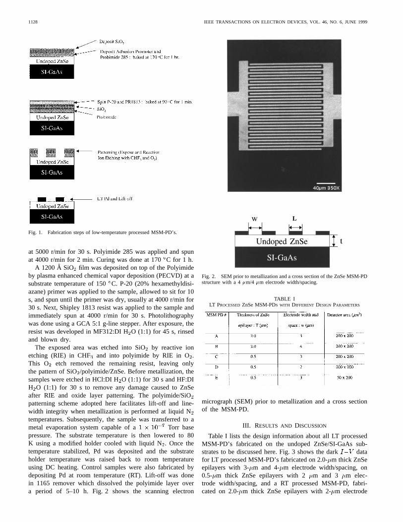
Fig. 1. Fabrication steps of low-temperature processed MSM-PD’s.
at 5000 r/min for 30 s. Polyimide 285 was applied and spunat 4000 r/min for 2 min. Curing was done at 170C for 1 h.
A 1200 A SiO film was deposited on top of the Polyimideby plasma enhanced chemical vapor deposition (PECVD) at asubstrate temperature of 150C. P-20 (20% hexamethyldisi-azane) primer was applied to the sample, allowed to sit for 10s, and spun until the primer was dry, usually at 4000 r/min for30 s. Next, Shipley 1813 resist was applied to the sample andimmediately spun at 4000 r/min for 30 s. Photolithographywas done using a GCA 5:1 g-line stepper. After exposure, theresist was developed in MF312:DI HO (1:1) for 45 s, rinsedand blown dry.
The exposed area was etched into SiOby reactive ionetching (RIE) in CHF and into polyimide by RIE in O.This O etch removed the remaining resist, leaving onlythe pattern of SiO/polyimide/ZnSe. Before metallization, thesamples were etched in HCl:DI HO (1:1) for 30 s and HF:DIH O (1:1) for 30 s to remove any damage caused to ZnSeafter RIE and oxide layer patterning. The polyimide/SiOpatterning scheme adopted here facilitates lift-off and line-width integrity when metallization is performed at liquid Ntemperatures. Subsequently, the sample was transferred to ametal evaporation system capable of a Torr basepressure. The substrate temperature is then lowered to 80K using a modified holder cooled with liquid N. Once thetemperature stabilized, Pd was deposited and the substrateholder temperature was raised back to room temperatureusing DC heating. Control samples were also fabricated bydepositing Pd at room temperature (RT). Lift-off was donein 1165 remover which dissolved the polyimide layer overa period of 5–10 h. Fig. 2 shows the scanning electron
Fig. 2. SEM prior to metallization and a cross section of the ZnSe MSM-PDstructure with a 4�m/4 �m electrode width/spacing.
TABLE ILT PROCESSEDZnSe MSM-PDS WITH DIFFERENT DESIGN PARAMETERS
micrograph (SEM) prior to metallization and a cross sectionof the MSM-PD.
III. RESULTS AND DISCUSSION
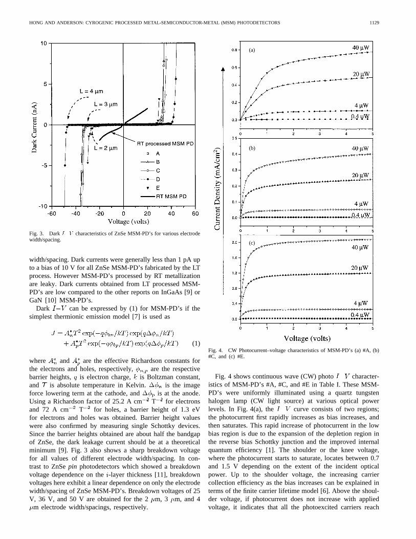
Table I lists the design information about all LT processedMSM-PD’s fabricated on the undoped ZnSe/SI-GaAs sub-strates to be discussed here. Fig. 3 shows the dark datafor LT processed MSM-PD’s fabricated on 2.0-m thick ZnSeepilayers with 3- m and 4- m electrode width/spacing, on0.5- m thick ZnSe epilayers with 2 m and 3 m elec-trode width/spacing, and a RT processed MSM-PD, fabri-cated on 2.0-m thick ZnSe epilayers with 2-m electrode
HONG AND ANDERSON: CYROGENIC PROCESSED METAL-SEMICONDUCTOR-METAL (MSM) PHOTODETECTORS 1129
Fig. 3. DarkI�V characteristics of ZnSe MSM-PD’s for various electrodewidth/spacing.
width/spacing. Dark currents were generally less than 1 pA upto a bias of 10 V for all ZnSe MSM-PD’s fabricated by the LTprocess. However MSM-PD’s processed by RT metallizationare leaky. Dark currents obtained from LT processed MSM-PD’s are low compared to the other reports on InGaAs [9] orGaN [10] MSM-PD’s.
Dark can be expressed by (1) for MSM-PD’s if thesimplest thermionic emission model [7] is used as
(1)
where and are the effective Richardson constants forthe electrons and holes, respectively, are the respectivebarrier heights, is electron charge, is Boltzman constant,and is absolute temperature in Kelvin. is the imageforce lowering term at the cathode, and is at the anode.Using a Richardson factor of 25.2 A cm T for electronsand 72 A cm T for holes, a barrier height of 1.3 eVfor electrons and holes was obtained. Barrier height valueswere also confirmed by measuring single Schottky devices.Since the barrier heights obtained are about half the bandgapof ZnSe, the dark leakage current should be at a theoreticalminimum [9]. Fig. 3 also shows a sharp breakdown voltagefor all values of different electrode width/spacing. In con-trast to ZnSepin photodetectors which showed a breakdownvoltage dependence on the-layer thickness [11], breakdownvoltages here exhibit a linear dependence on only the electrodewidth/spacing of ZnSe MSM-PD’s. Breakdown voltages of 25V, 36 V, and 50 V are obtained for the 2m, 3 m, and 4
m electrode width/spacings, respectively.
(a)
(b)
(c)
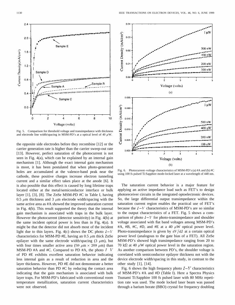
Fig. 4. CW Photocurrent–voltage characteristics of MSM-PD’s (a) #A, (b)#C, and (c) #E.
Fig. 4 shows continuous wave (CW) photo character-istics of MSM-PD’s #A, #C, and #E in Table I. These MSM-PD’s were uniformly illuminated using a quartz tungstenhalogen lamp (CW light source) at various optical powerlevels. In Fig. 4(a), the curve consists of two regions;the photocurrent first rapidly increases as bias increases, andthen saturates. This rapid increase of photocurrent in the lowbias region is due to the expansion of the depletion region inthe reverse bias Schottky junction and the improved internalquantum efficiency [1]. The shoulder or the knee voltage,where the photocurrent starts to saturate, locates between 0.7and 1.5 V depending on the extent of the incident opticalpower. Up to the shoulder voltage, the increasing carriercollection efficiency as the bias increases can be explained interms of the finite carrier lifetime model [6]. Above the shoul-der voltage, if photocurrent does not increase with appliedvoltage, it indicates that all the photoexcited carriers reach
1130 IEEE TRANSACTIONS ON ELECTRON DEVICES, VOL. 46, NO. 6, JUNE 1999
Fig. 5. Comparison for threshold voltage and transimpedance with thicknessand electrode line width/spacing in MSM-PD’s at a optical level of 40�W.
the opposite side electrodes before they recombine [12] or thecarrier generation rate is higher than the carrier sweep-out rate[13]. However, perfect saturation of the photocurrent is notseen in Fig. 4(a), which can be explained by an internal gainmechanism [1]. Although the exact internal gain mechanismis moot, it has been postulated that when photo-generatedholes are accumulated at the valence-band peak near thecathode, these positive charges increase electron tunnelingcurrent and a similar effect takes place at the anode [6]. Itis also possible that this effect is caused by long lifetime trapslocated either at the metal/semiconductor interface or bulklayer [1], [3], [8]. The ZnSe MSM-PD #C in Table I, having0.5 m thickness and 3 m electrode width/spacing with thesame active area as #A showed the improved saturation currentin Fig. 4(b). This result supported the theory that the internalgain mechanism is associated with traps in the bulk layer.However the photocurrent (detector sensitivity) in Fig. 4(b) atthe same incident optical power is less than in Fig. 4(a). Itmight be that the detector did not absorb most of the incidentlight due to thin layers. Fig. 4(c) shows the DC photocharacteristics for MSM-PD #E, having an 0.5m thick ZnSeepilayer with the same electrode width/spacing (3m), butwith four times smaller active area ( m m) thanMSM-PD #A and #C. Compared to PD #A, the photoof PD #E exhibits excellent saturation behavior indicatingless internal gain as a result of reduction in area and thelayer thickness. However, PD #E did not demonstrate a bettersaturation behavior than PD #C by reducing the contact areaindicating that the gain mechanism is associated with bulklayer traps. For MSM-PD’s fabricated with conventional roomtemperature metallization, saturation current characteristicswere not observed.
(a)
(b)
Fig. 6. Photocurrent–voltage characteristics of MSM-PD’s (a) #A and (b) #Cusing 100 fs pulsed Ti:Sapphire mode-locked laser at a wavelength of 448 nm.
The saturation current behavior is a major feature forapplying an active impedance load such as FET’s to designphotoreceiver circuits in the integrated optoelectronic devices.So, the large differential output transimpedance within thesaturation current region enables the practical use of FET’sbecause the characteristics of MSM-PD’s are so similarto the output characteristics of a FET. Fig. 5 shows a com-parison of photo for photo-transimpedance and shouldervoltage associated with flat band voltages among MSM-PD’s#A, #B, #C, #D, and #E at a 40W optical power level.Photo-transimpedance is given by at a certain opticalpower level (analogous to the gate bias of a FET). All ZnSeMSM-PD’s showed high transimpedance ranging from 20 to70 k at 40 W optical power level in the saturation region.As another comparison between PD’s, the shoulder voltage iscorrelated with semiconductor epilayer thickness not with thedevice electrode width/spacing in this study, in contrast to theother study [1], [14].
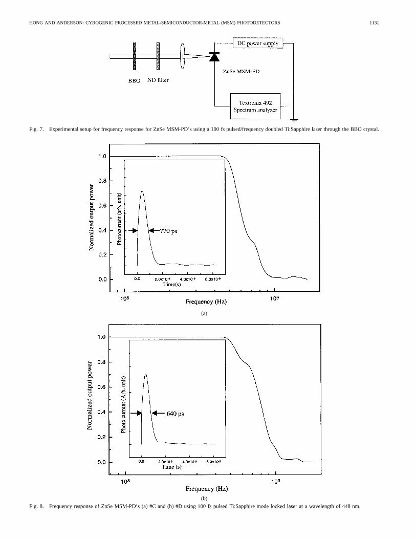
Fig. 6 shows the high frequency photo characteristicsof MSM-PD’s #A and #D (Table I). Here a Spectra PhysicsTsunami Ti:Sapphire 100 fs pulsed laser with 80 MHz repeti-tion rate was used. The mode locked laser beam was passedthrough a barium borate (BBO) crystal for frequency doubling
HONG AND ANDERSON: CYROGENIC PROCESSED METAL-SEMICONDUCTOR-METAL (MSM) PHOTODETECTORS 1131
Fig. 7. Experimental setup for frequency response for ZnSe MSM-PD’s using a 100 fs pulsed/frequency doubled Ti:Sapphire laser through the BBO crystal.
(a)
(b)
Fig. 8. Frequency response of ZnSe MSM-PD’s (a) #C and (b) #D using 100 fs pulsed Ti:Sapphire mode locked laser at a wavelength of 448 nm.
1132 IEEE TRANSACTIONS ON ELECTRON DEVICES, VOL. 46, NO. 6, JUNE 1999
leading to a wavelength of 448 nm, above the ZnSe bandgapenergy. The full width half maximum (FWHM) of laser beamsize is around m , which is six times larger thanthe active area of the MSM-PD’s. Therefore, optical powercaptured by the detector is smaller than the power mentioned inFig. 6. Comparing this to the CW photo characteristics,the saturation behavior at higher bias voltage in Fig. 6(a) isnot good. Reducing the thickness of the bulk layer showed alittle better saturation behavior but still worse than in the CWphotocurrent saturation data. However, reducing the electrodewidth/spacing did not improve the saturation (internal gainwas not influenced) for the high frequency photoresponse.This result again supports the theory that the internal gainin the ZnSe MSM-PD’s may be due to long lifetime trapsin the bulk layer rather than at the metal/semiconductorinterface.
Fig. 7 shows the schematic experimental setup for frequencyresponse based on impulse response with the assumptionof the input optical signal as a train of delta functions.Impulse response of the MSM-PD’s was obtained by opticalexcitation with a 100 fs pulsed mode locked Ti:Sapphirelaser at a wavelength of 448 nm. The output signal wasdetected by a Tektronix 492 spectrum analyzer. Taking Fouriertransformation, the temporal response for the MSM-PD’s canbe obtained.
Fig. 8 shows the frequency response of ZnSe MSM-PD’s(a) #C and (b) #D and their Fourier transformed temporalresponse in insets to the 100 fs pulse laser input having80 MHz repetition rate. The 3 m MSM-PD showed a 3dB frequency of 620 MHz and its associated temporal pulsewidth (FWHM) of 770 ps. The 2 m device demonstrateda 3 dB frequency of 800 MHz and its corresponding pulsewidth of 640 ps. FWHM’s of pulse width were obtainedby taking the Fourier transform of frequency response. Thefrequency response showed that the 2m device had improveddevice speed due to the short carrier transit time betweenelectrodes.
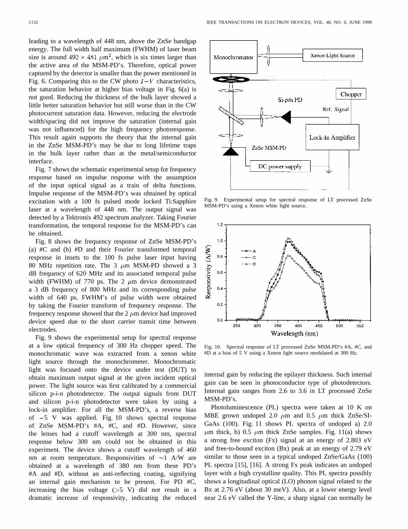
Fig. 9 shows the experimental setup for spectral responseat a low optical frequency of 300 Hz chopper speed. Themonochromatic wave was extracted from a xenon whitelight source through the monochrometer. Monochromaticlight was focused onto the device under test (DUT) toobtain maximum output signal at the given incident opticalpower. The light source was first calibrated by a commercialsilicon p-i-n photodetector. The output signals from DUTand silicon p-i-n photodetector were taken by using alock-in amplifier. For all the MSM-PD’s, a reverse biasof 5 V was applied. Fig. 10 shows spectral responseof ZnSe MSM-PD’s #A, #C, and #D. However, sincethe lenses had a cutoff wavelength at 300 nm, spectralresponse below 300 nm could not be obtained in thisexperiment. The device shows a cutoff wavelength of 460nm at room temperature. Responsivities of1 A/W areobtained at a wavelength of 380 nm from these PD’s#A and #D, without an anti-reflecting coating, signifyingan internal gain mechanism to be present. For PD #C,increasing the bias voltage (5 V) did not result in adramatic increase of responsivity, indicating the reduced
Fig. 9. Experimental setup for spectral response of LT processed ZnSeMSM-PD’s using a Xenon white light source.
Fig. 10. Spectral response of LT processed ZnSe MSM-PD’s #A, #C, and#D at a bias of 5 V using a Xenon light source modulated at 300 Hz.
internal gain by reducing the epilayer thickness. Such internalgain can be seen in photoconductor type of photodetectors.Internal gain ranges from 2.6 to 3.6 in LT processed ZnSeMSM-PD’s.
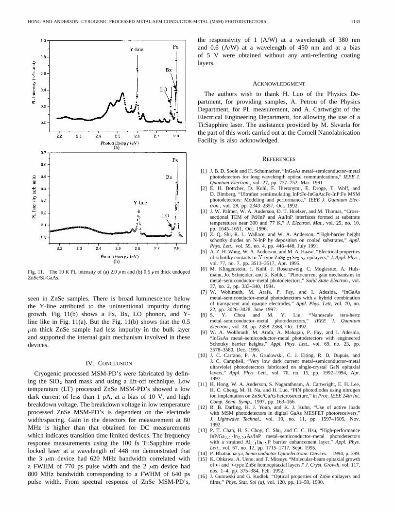
Photoluminescence (PL) spectra were taken at 10 K onMBE grown undoped 2.0 m and 0.5 m thick ZnSe/SI-GaAs (100). Fig. 11 shows PL spectra of undoped a) 2.0
m thick, b) 0.5 m thick ZnSe samples. Fig. 11(a) showsa strong free exciton (Fx) signal at an energy of 2.803 eVand free-to-bound exciton (Bx) peak at an energy of 2.79 eVsimilar to those seen in a typical undoped ZnSe/GaAs (100)PL spectra [15], [16]. A strong Fx peak indicates an undopedlayer with a high crystalline quality. This PL spectra possiblyshows a longitudinal optical (LO) phonon signal related to theBx at 2.76 eV (about 30 meV). Also, at a lower energy levelnear 2.6 eV called the Y-line, a sharp signal can normally be
HONG AND ANDERSON: CYROGENIC PROCESSED METAL-SEMICONDUCTOR-METAL (MSM) PHOTODETECTORS 1133
(a)
(b)
Fig. 11. The 10 K PL intensity of (a) 2.0�m and (b) 0.5�m thick undopedZnSe/SI-GaAs.
seen in ZnSe samples. There is broad luminescence belowthe Y-line attributed to the unintentional impurity duringgrowth. Fig. 11(b) shows a Fx, Bx, LO phonon, and Y-line like in Fig. 11(a). But the Fig. 11(b) shows that the 0.5
m thick ZnSe sample had less impurity in the bulk layerand supported the internal gain mechanism involved in thesedevices.
IV. CONCLUSION
Cryogenic processed MSM-PD’s were fabricated by defin-ing the SiO hard mask and using a lift-off technique. Lowtemperature (LT) processed ZnSe MSM-PD’s showed a lowdark current of less than 1 pA, at a bias of 10 V, and highbreakdown voltage. The breakdown voltage in low temperatureprocessed ZnSe MSM-PD’s is dependent on the electrodewidth/spacing. Gain in the detectors for measurement at 80MHz is higher than that obtained for DC measurementswhich indicates transition time limited devices. The frequencyresponse measurements using the 100 fs Ti:Sapphire modelocked laser at a wavelength of 448 nm demonstrated thatthe 3 m device had 620 MHz bandwidth correlated witha FWHM of 770 ps pulse width and the 2m device had800 MHz bandwidth corresponding to a FWHM of 640 pspulse width. From spectral response of ZnSe MSM-PD’s,
the responsivity of 1 (A/W) at a wavelength of 380 nmand 0.6 (A/W) at a wavelength of 450 nm and at a biasof 5 V were obtained without any anti-reflecting coatinglayers.
ACKNOWLEDGMENT
The authors wish to thank H. Luo of the Physics De-partment, for providing samples, A. Petrou of the PhysicsDepartment, for PL measurement, and A. Cartwright of theElectrical Engineering Department, for allowing the use of aTi:Sapphire laser. The assistance provided by M. Skvarla forthe part of this work carried out at the Cornell NanofabricationFacility is also acknowledged.
REFERENCES
[1] J. B. D. Soole and H. Schumacher, “InGaAs metal–semiconductor–metalphotodetectors for long wavelength optical communications,”IEEE J.Quantum Electron., vol. 27, pp. 737–752, Mar. 1991
[2] E. H. Bottcher, D. Kuhl, F. Hieronymi, E. Droge, T. Wolf, andD. Bimberg, “Ultrafast semiinsulating InP:Fe-InGaAs:Fe-InP:Fe MSMphotodetectors: Modeling and performance,”IEEE J. Quantum Elec-tron., vol. 28, pp. 2343–2357, Oct. 1992.
[3] J. W. Palmer, W. A. Anderson, D. T. Hoelzer, and M. Thomas, “Cross-sectional TEM of Pd/InP and Au/InP interfaces formed at substratetemperatures near 300 and 77 K,”J. Electron. Mat., vol. 25, no. 10,pp. 1645–1651, Oct. 1996.
[4] Z. Q. Shi, R. L. Wallace, and W. A. Anderson, “High-barrier heightschottky diodes on N-InP by deposition on cooled substrates,”Appl.Phys. Lett., vol. 59, no. 4, pp. 446–448, July 1991.
[5] A. Z. H. Wang, W. A. Anderson, and M. A. Haase, “Electrical propertiesof schottky contacts toN -type ZnS0:07Se0:93 epilayers,”J. Appl. Phys.,vol. 77, no. 7, pp. 3513–3517, Apr. 1995.
[6] M. Klingenstein, J. Kuhl, J. Rosenzweig, C. Moglestue, A. Huls-mann, Jo. Schneider, and K. Kohler, “Photocurrent gain mechanisms inmetal–semiconductor–metal photodetectors,”Solid State Electron., vol.37, no. 2, pp. 333–340, 1994.
[7] W. Wohlmuth, M. Arafa, P. Fay, and I. Adesida, “InGaAsmetal–semiconductor–metal photodetectors with a hybrid combinationof transparent and opaque electrodes,”Appl. Phys. Lett, vol. 70, no.22, pp. 3026–3028, June 1997.
[8] S. Y. Chou and M. Y. Liu, “Nanoscale tera-hertzmetal–semiconductor–metal photodetectors,”IEEE J. QuantumElectron., vol. 28, pp. 2358–2368, Oct. 1992.
[9] W. A. Wohlmuth, M. Arafa, A. Mahajan, P. Fay, and I. Adesida,“InGaAs metal–semiconductor–metal photodetectors with engineeredSchottky barrier heights,”Appl. Phys. Lett., vol. 69, no. 23, pp.3578–3580, Dec. 1996.
[10] J. C. Carrano, P. A. Grudowski, C. J. Eiting, R. D. Dupuis, andJ. C. Campbell, “Very low dark current metal–semiconductor–metalultraviolet photodetectors fabricated on single-crystal GaN epitaxiallayers,” Appl. Phys. Lett., vol. 70, no. 15, pp. 1992–1994, Apr.1997.
[11] H. Hong, W. A. Anderson, S. Nagarathnam, A. Cartwright, E. H. Lee,H. C. Cheng, M. H. Na, and H. Luo, “PIN photodiodes using nitrogenion implantation on ZnSe/GaAs heterostructure,” inProc. IEEE 24th Int.Comp. Semi. Symp., 1997, pp. 163–166.
[12] R. B. Darling, H. J. Youn, and K. J. Kuhn, “Use of active loadswith MSM photodetectors in digital GaAs MESFET photoreceivers,”J. Lightwave Technol., vol. 10, no. 11, pp. 1597–1605, Nov.1992.
[13] P. T. Chan, H. S. Choy, C. Shu, and C. C. Hsu, “High-performanceInP/Ga0:47In0:53As/InP metal–semiconductor–metal photodetectorswith a strained Al0:1In0:9P barrier enhancement layer,”Appl. Phys.Lett., vol. 67, no. 12, pp. 1715–1717, Sept. 1995.
[14] P. Bhattacharya,Semiconductor Optoelectronic Devices. 1994, p. 399.[15] K. Ohkawa, A. Ueno, and T. Mitsuyu “Molecular-beam epitaxial growth
of p- andn-type ZnSe homoepitaxial layers,”J. Cryst. Growth, vol. 117,nos. 1–4, pp. 375–384, Feb. 1992.
[16] J. Gutowski and G. Kudlek, “Optical properties of ZnSe epilayers andfilms,” Phys. Stat. Sol (a), vol. 120, pp. 11–59, 1990.

1134 IEEE TRANSACTIONS ON ELECTRON DEVICES, VOL. 46, NO. 6, JUNE 1999
Hyesook Hong received the B.S. degree in elec-tronics engineering from Sung Kyun Kwan Uni-versity, Suwon, Korea, in 1983, the M.S. degreein electrical engineering from the University ofColorado, Boulder, in 1991, and the Ph.D. degree inelectrical engineering from State University of NewYork at Buffalo in 1998. Her Ph.D. work focusedon characterization, fabrication, and applications ofZnSe devices.
From 1983 to 1989, she was with the KoreaTelecommunication Authority as a Software En-
gineer. In 1998, she joined Headway Technologies, Inc., Milpitas, CA.Her current interests are fabrication, modeling, and characterization forsemiconductor devices.
Wayne A. Anderson(S’68–M’70–SM’82) receivedthe Ph.D. in electrical engineering in 1970, with anemphasis in semiconductors and microwaves.
His experience includes industrial R&D(1962–1965), and university teaching(1966–present) with eight years at RutgersUniversity and the remaining at State University ofNew York at Buffalo. His present research interestsinclude thin-film resistors and capacitors, thin-filmsilicon for solar cells and flat panel displays, andmetallization of wide-bandgap semiconductors.
He has supervised the completion of 44 M.S. or Ph.D. theses/dissertationsand coauthored over 200 conference presentations as well as over 150journal articles.
Prof. Anderson is a member of APS and MRS.

![Light Sources and Photodetectors Enabled by 2D Semiconductorsyuting/Publications/Publication 2018/Light... · semiconductors such as 1L transition-metal dichalcogenides (TMDs),[9–14]](https://img.pdfslide.us/doc/110x75/6061bdc8bd373d4e7371e469/light-sources-and-photodetectors-enabled-by-2d-yutingpublicationspublication-2018light.jpg)