Embed Size (px)
Citation preview

Cryogenic Applications of Commercial Electronic Components
Ernest D. Buchanan, 1 Dominic J. Benford,2 Joshua B. Forgione,3 S. Harvey Moseley,2 and Edward J. Wollack2
I ADNET Systems Inc., 164 Rollins Avenue Suite 303, Rockville, MD, 20852, USA Z NASA / Goddard Space Flight Center, Greenbelt, MD, 20771, USA 3 NASA / Ames Research Center, Moffett Field, CA 94035, USA
We have developed a range of techniques useful for constructing analog and digital circuits for operation in a liquid Helium environment (4.2K), using commercially available low power components. The challenges encountered in designing cryogenic electronics include finding components that can function usefully in the cold and possess low enough power dissipation so as not to heat the systems they are designed to measure. From design, test, and integration perspectives it is useful for components to operate similarly at room and cryogenic temperatures; however this is not a necessity. Some of the circuits presented here have been used successfully in the MUSTANG l and in the GISM02 camera to build a complete digital to analog multiplexer (which will be referred to as the Cryogenic Address Driver board). Many of the circuit elements described are of a more general nature rather than specific to the Cryogenic Address Driver board, and were studied as a part of a more comprehensive approach to addressing a larger set of cryogenic electronic needs.
Introduction
In this paper, we describe an implementation of the Cryogenic Address Driver board. This description should enable an experimenter to fulfill a variety of instrumentation needs based on the chip set presented that will function at liquid Helium temperatures. No attempt will be made to analyze the inner workings of the integrated circuits that work at 4.2 K as we are at the mercy of the chip manufacturer's whim, and parts that passed our tests may not work in future lots. Most manufacturers' low temperature specifications end at -40 C (233K). We first describe experimental techniques and fixtures used for the characterization of candidate components. Next we provide specific details for acceptable components and lastly we provide detailed evaluation of an implementation using those components. Extended laboratory and observational use of the Cryogenic Address Driver board has shown the robustness of the techniques. All measurements presented in this paper were made in (submerged) liqnid Helium at 4.2 K unless otherwise noted.
A Fixture for Liquid Helium Electronic Tests
A probe assembly was built to submerge the various components and assemblies into liquid Helium. It consists of a room temperature (BNC connector) junction box, a long thin wall stainless steel tube, and a proto-board test area at the bottom as shown in Fig. 1. Cables can run either inside the tube or be attached to the outside with Kapton3 5413 tape.
For high bandwidth tests in liquid Helium, two conditions must be satisfied: thermal isolation and RF impedance uniformity. Ideally, copper coaxial cable would .be run from the 4.2
1
https://ntrs.nasa.gov/search.jsp?R=20120013044 2020-06-01T17:25:55+00:00Z

K portion of the Dewar to the room temperature test equipment. The heat load from the copper cable might be prohibitive for long term testing, and would probably result in the test board's temperature being higher than 4.2 K, as well as creating gradients across parts along with poor thermal stability. Our solution was a thermal break of very small diameter stainless-steel coax (LakeShore4 CC-SS), about 5 cm long, just above the liquid Helium level.
4 EACH BN (ONLY ONE
FOR CLAR
C FEMALES COAX SHOWN
ITY)
LOOSE FITT
l-e° DIAME STAINLESS
ING LID ~
lER THIll WALL L
STEEL TUBING
RG-316/U
STAINLESS LAKE SHORE
STEEL COAX
RG-316/u
TEST BOAR
DEVICE UND
DUNK DEWA
D
R
TYPE CC-SS
ER lEST
0
't:
-
0 0
r-
-
:J ~
r'
FR-4 CIRCUIT BOARD
FIG. 1. Layout of the component test system.
The bridge added significant crosstalk to measurements, but performed well enough to allow measurement of the amplitude of the signal after ringing ceased. Comparisons were made at room temperature to ensure that observed spikes were from the bridge and not from coldrelated problems. All remaining RF cable in Helium (and above the bridge) is RG/316 Teflon dielectric (silver-plated, copper conductors). DC power and bias are supplied by twisted pair O.OlD" Manganin wire. A subset of tests were made without the use of the bridge by using RG-316U cable from device-under-test to room temperature instruments; smaller signals could be observed at a penalty of greater liquid Helium consumption.
The Helium reservoir is a dunking Dewar made by Precision Cryogenics, Incorporateds. No vacuum is required in the space above the liquid level, and is thus very simple to use. A loose-fitting cover is used to enable Helium boil-off gas to purge the working volume. Once the Dewar is filled (about 0.5 m deep) with Helium, the probe and device-under-test can be lowered into the liquid. Test device temperatures can go to 4.2 K as quickly as the experimenter will dare. The probe is usually lowered into Helium in less than five minutes.
A simpler solution for component and small board testing uses an inexpensive Pope6
8645/0099 1000 ml glass Dewar. Due to its small 7 cm internal diameter very little Helium is required, and Dewar cool-down is faster. The capacity of this Dewar makes the Helium hold time short (2 to 4 minutes with one cooldown), but generally long enough for useful measurement. The electrical techniques are otherwise identical to those used with the Precision Cryogenics Dewar.
2
Test of the Analog Switches
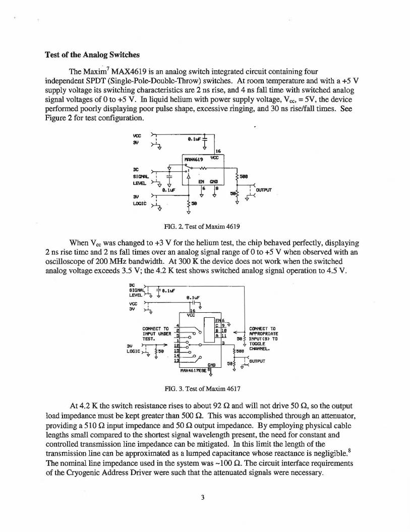
The Maxi~7 MAX4619 is an analog switch integrated circuit containing four independent SPOT (Single-Pole-Double-Throw) switches. At room temperature and with a +5 V supply voltage its switching characteristics are 2 ns rise, and 4 ns fall time with switched analog signal voltages of 0 to +5 V. In liquid helium with power supply voltage, V ce, = 5V, the device performed poorly displaying poor pulse shape, excessive ringing, and 30 ns rise/fall times. See Figure 2 for test configuration.
.. 1'IIC4619 YCC
DC
8.-" , T l£\6. >-"¢ ....,
a. LIE'
L..OC:lC "" FIG. 2. Test of Maxim 4619
When Vee was changed to +3 V for the helium test, the chip behaved perfectly, displaying 2 ns rise time and 2 ns fall times over an analog signal range of 0 to +5 V when observed with an oscilloscope of 200 MHz bandwidth. At 300 K the device does not work when the switched analog voltage exceeds 3.5 V; the 4.2 K test shows switched analog signal operation to 4.5 V.
DC SIGI1AL~ T 8.1uF LEVEL' <r v 8.1uF I'CC 3Y
""',---n~ >-'<,
YCC
COHHECT TO INPUT UNlER -:1---0 TEST.
~OO'C~ F COHt£CT TO APPROPRIATE
~e INPUT(S> TO U[~.~~~~-. T~E
:588 Ctwf'tEL.
GItD I'IA)(461 ?ESE
SO j<0UTPUT
FIG. 3. Test of Maxim 4617
At 4.2 K the switch resistance rises to about 92 n and will not drive 50 n, so the output load impedance muSt be kept greater than 500 n. This was accomplished through an attenuator, providing a 510 n input impedance and 50 n output impedance. By employing physical cable lengths small compared to the shortest signal wavelength present, the need for constant and controlled transmission line impedance can be mitigated. In this limit the length of the transmission line can be approximated as a lumped capacitance whose reactance is negligible.8
The nominal line impedance used in the system was -lOOn. The circuit interface requirements of the Cryogenic Address Driver were such that the attenuated signals were necessary.
3

The Maxim MAX4617 analog switch integrated circuit was tested for signal quality on each of its eight outputs exactly as the MAX4619 was tested. Figures 3 and 4 show the test setup and observed linearity respectively. Overall board performance is displayed by the oscillogram in Figure 5.
MAXIM 4617 --_ . . - ... .. _ .... _ ... _ . ...
600
200
o .. .-:.. .. - .. ~.~. -- .. _ .. _. _ .. --- -_ .. .. __ .-.'. o 2 4 5
Output [Volts]
• 300K Vdd = 3.31 V • 4.2K Vdc = 3.29V
FlG. 4. Linearity of the switehed analog signal through a MAXIM 4617 •
• .
-j -". ~-+
. . Mf.boirii 'Ctil :.t .. . :....·fmv:
FIG. 5. Oscillogram of Maxim 4617 Output. The signal shown is the analog output of the circuit shown in Figure 3. In our implementation, the expected level is 70 mV and the rise/fall times are of acceptable duration.
4

Tests of TTL Logic Chips
A variety of 1TL (Transistor-Transistor Logic) chips were tested for use on various Cryogenic Address Driver Board designs: 74AC02N (quad 2 input NOR gate), 74AC08 (quad 2 input AND gate), and the MC74ACI38N (1 of 8 demultiplexer) and the 74HCl74N (hex D flipflop). The power supply voltage and various logical threshold levels were tested for rise-time and pulse shape. ON Semiconducto? (Motorola) and Fairchild lO parts have been used interchangeably with no problems. See Figures 6, 7, and 8 for test configurations. At 4.2K we have used the values shown in Table I, for detailed room nominal temperamre operational parameters consult the vendor specification.
TABLE t MC74ACI38N PARMfuTERS
Logic Temperature Vee Threshold (Kelvin) (VollS) (VollS)
293 5 2.5 4.2 5 2.3 4.2 4 1.8 4.2 3 1.4
Rise Fall Time Time Output (osec) (nsee) (VollS)
1.2 1.2 5.0 3 3 4.6 5 3 3.9 5 3 2.8
+3Y , >-'v 10.
:K! LOGIC , JIf'UT >-'v
ENABLE~
74ACI3BN B
FIG. 6. Test of74AC138
e.luF
+3Y ~,--...-1""1
>-'v 50 LOGIC , INPUT ~
1 14 1"3,---,
10k
LOW SPEED 74AC0S
IIf'UT ~ J0.luF
FIG. 7. Test of 74AC08
5
10k OUTPUT
50 ,
,f-<
OUTPUT
, ,f-<
II. lui' >-r---------,----lh
+~ I .q ~
LOGIC >-r-----;r:----"'-I I , INPUT~ I Ilk
LOW SPEED 74AC02
INPUT ~ JII.luF
FIG. 8. Test of 74AC02
OUTPUT .
,f-<
FET Voltage Reference Test
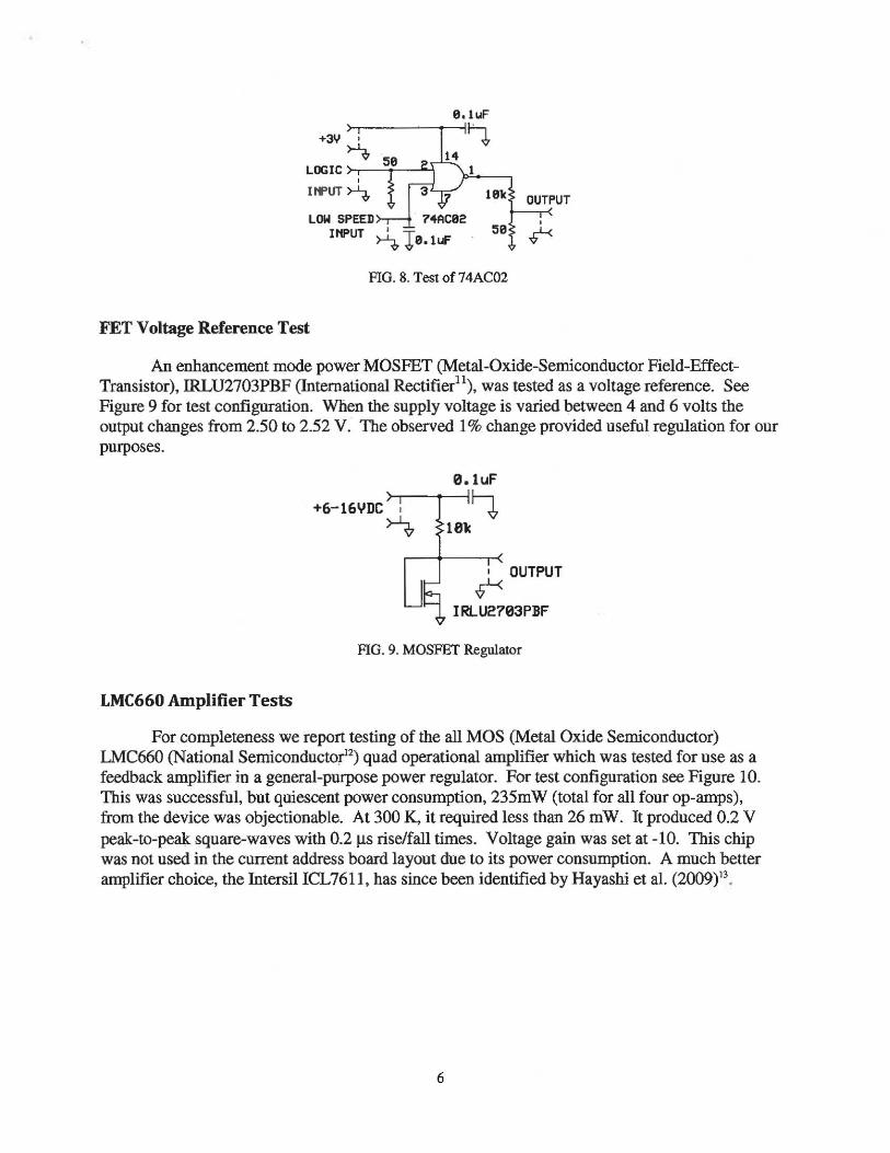
An enhancement mode power MOSFET (Metal-Oxide-Semiconductor Field-EffectTransistor), IRLU2703PBF (International Rectifierll), was tested as a voltage reference. See Figure 9 for test configuration. When the supply voltage is varied between 4 and 6 volts the output changes from 2.50 to 2.52 V. The observed 1 % change provided useful regulation for our purposes.
0.1uF
+6-16YDC ,
>-1, ~
10lc
, OUTPUT ,f-<
IRLU2703PBF
FIG. 9. MOSFET Regulator
LMC660 Amplifier Tests
For completeness we report testing of the all MOS (Metal Oxide Semiconductor) LMC660 (National Semiconductor12
) quad operational amplifier which was tested for use as a feedback amplifier in a general-purpose power regulator. For test configuration see Figure 10. This was successful, but quiescent power consumption, 235mW (total for all four op-amps), from the device was objectionable. At 300 K, it required less than 26 mW. It produced 0.2 V peak-to-peak square-waves with 0.2 ~ rise/fall times. Voltage gain was set at -10. This chip was not used in the current address board layout due to its power consumption. A much better amplifier choice, the Intersil ICL 7611, has since been identified by Hayashi et al. (2009)13.
6

e.1u1'
+:5'.' • I¢ ~
It OUTPUT INPUT , ~
, e.1u1' r ,:511 ~
FIG. 10. LMC660N Test Setup
Cryogenic Back-Tennination
For high-speed pulse fidelity, transmission lines must be terminated in their characteristic impedance. If not terminated properly, reflections can create multiple logic triggers, or make analog signals unreadable. If 50 Q resistors terminated the Cryogenic Address Driver board's input lines, they would add about 70 mW per input channel for 100% duty cycle DC signals. Back-termination is a technique which can reduce this power dissipation by a factor of _104
. It functions by absorbing the reflected wave at the room temperature generator instead of the cryogenic receiving end. See Figures 11 and 12 for test configurations employed. The observed response was better than anticipated with open or short circuited radio frequency transmission line. Cryogenic radio frequency/logic systems can benefit from back termination due to smaller cryogenic heat loading, as .the termination impedance can be zero or infinite.
OSCILLOSCOPE
r+--;;.-;O""HM"'s-' 42 OHPlS 20 = 58 OHI'IS o INPUT
FIG. 11. Back tennination open test
FIG. 12. Back tennination short test
Two experiments were performed to measure back-terminated signal fidelity. The first was a simple open circuit into a high- impedance 100 MHz oscilloscope input. Twelve feet of RG58 and RG 174 (both 50 n Zo lines) were used to see if line loss could have an effect. A pulse amplifier utilizing the 4619 Maxim FET analog switch was employed, with a rise-time smaller than 5 ns. The output impedance of the switch was measured on an Agi1ent14 4284A LCR (lnductance-Capacitance-Resistance) bridge at 1 MHz, and found to be about 8 Q in both high and low states. To bring backward reflections near zero, 42 Q were added in series to the output of the switch (8 n +42 n = 50 Q). Measured ringing was about 15% of the signal amplitude.
A (2 n) short circuit test showed good results, limited by the quality of the constructed short circuit. Five 10 Q RN55D resistors were placed in parallel with leads as short as practical.
7

LCR bridge measurements indicate an impedance of 50 Q + jO.l Qat 1 MHz. Scaling the measured reactance from 1 MHz one finds X - +j6 Q at 60 MHz, which accounts for the <20% ringing observed on the signal. A lower inductance load would reduce the ringing from reflections. The short 50 Q section to the oscilloscope is terminated again to prevent ringing.
In our experience if the line approaches either an ideal open circuit (in this case -5 pF) or short-circuit the system will work well. Varying inductance in the short-circuited version shows variation in ringing. Any practical and purely real resistance (0 to 4 Q) at the termination end was observed to produce square pulses.
Printed Circuit Board Design and Capacitors
The surface mount technology printed circuit board for the final product is 0.0625" double-sided FR-4 (relative dielectric constant, €,-'" 4.3). Careful attention was paid to keeping trace impedances controlled. Also, good DC bypassing is present on all chips. All capacitors are 0.1 JJF, Kemee' C0603CI04J3RAC-TU. The value changes to approximately 0.005 IlF at 4.2 K (the values shown on schematics in this paper are the manufacturer's stated room temperature magnitude, not the cold value). Generally a capacitor with a simple dielectric (e.g., porcelain, alumina, quartz, etc.) will change significantly less than the high dielectric constant (X7R) types. This is due to the change in the dielectric permittivity with temperature and can make identification of appropriate components with capacitance> 1 nF challenging.
Resistors
The resistors are a special temperature compensating metal film type: Vishay 16
1NPW0603 series. The largest temperature dependent resistance change was 0.8 % (from 300 K to 4.2 K) on a sample of 30 resistors, of four different resistor values. The 500 Q resistor in the output circuit was not a 1NPW 1206 due to minimum order quantities; an available resistor variety (Vishay, thick film CRCWI206) was substituted. To provide the appropriate value for operation at 4.2 K, this resistor was changed to 294 Q. CRCW series resistors have stable resistance values once placed in liquid Helium. There are other resistor vendors but the type we would recorrunend would be constructed from thin-film disordered alloys. Vishay also produces thick-film RCWP series ruthenium oxide resistors which are useful as thermistors below 4.2K17
•
Inductor
A 0402 size Taiyo Yuden18 chip inductor was tested for possible use as a filter component. At 300 K the inductance was measured at 2.228 !J.H falling to 1.37 !J.H with a series resistance of 0.96 Q at 4.2 K. An analysis of the coil indicates that it is wound on a core of magnetic material whose permeability changes when cooled. Where possible we would recommend use an air-wound coil since only the parasitic resistance changes; however, the inductor described has the advantage that it occupies much less space on the board.
Light Emitting Diode
A red light emitting diode (LED) is used as an illuminating bias source in the WMAPI9
spacecraft preamplifiers. One of the few successful packaged devices known operate at 4.2 K is
8

a DialighfO 521-9186 (also known as the RL50 or MV50). The device is operated at constant current of 2 rnA. The required voltage is observed to shift from 1.6 V to 1.9 V in cooling from room temperature to 4.2 K.
Address Driver Board General Description
The Cryogenic Address Driver board we developed operates at temperatures down to 4.2 K providing rapid switching of time-division Super Conducting Quantum Interference Device (SQUID) multiplexers. SQUID multiplexers are used to read out arrays of superconducting transition edge sensor bolometers 21. The driver board uses commercially available electronic components selected to operate in liquid Helium, and is operated by means of an associated highspeed controller running at room temperamre. The address wiring count for n multiplexed channels is reduced from n to /og2n+3, and the transmission of digital and analog signals with fast rise times into a cryogenic environment is simplified.
The control signals required by the SQUID multiplexer are in the millivolt range, and the transmission degradation of those signals would be serious. A simple DC level is sent to the analog switches which produce clean rectangular waves controlled by digital signals. Also, our 32 address requirement becomes 8 channels instead of 32, reducing the conductive parasitic load into the cryogenic environment. Operating at 4.2 K, the address driver feamres a 2 ns rise and 2 ns fall time when switching, and has been tested with up to 32 addresses. This approach will reduce electrical noise and ringing due to the proximity of the driver to the 8 milliohm SQUIDS when appropriately back terminated.
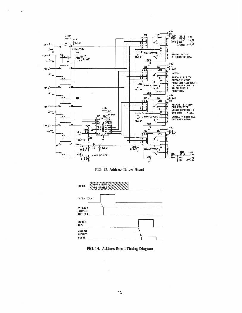
The Cryogenic Address Driver was built on a 2 layer FR-4 printed circuit board and consists of a digital interface and an analog output section (see Figures 13 and 16). Five edge triggered flip-flops are used as an input digital register. The value stored in this register determines which output channel will be enabled; the register is loaded by a clock pulse. Board logic using a TTL gate demultiplexer, 74AC138, allows only one MAX4617 to be selected at a time.
Maxim MAX4617 eight position analog switches route the reference voltage input, Vref,
to a "Tee" attenuator to produce analog voltage outputs. The "Tee" attenuator (RA, RB and RC) provides both proper loading of the Maxim chip and back termination for reflected waves. A resistor-capacitor filtered (R9, C3) input is provided for the demultiplexed output signal. Output voltage will be in direct proportion to V ref.
Digital circuits consist of a 6 bit register (74ACI74SC) and a 4 bit demultiplexer (74AC138D). The register ensures against logic races when used with the enable bit, as seen in Figure 14. The demultiplexer selects individual Maxim analog switches with a minimum of control lines.
System Level Address Driver Tests
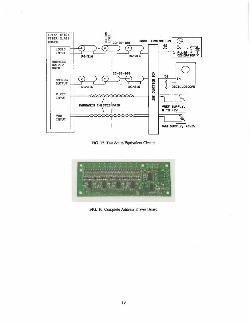
The Cryogenic Address Driver board was tested in a liqujd Helium dunking dewar driven by the room temperature timing electronics" (see oscillogram in Figure 5). A Kapton/Manganin stripline cable of 50 Q characteristic impedance interconnected the two boards. Mangauin, an alloy of copper and magnesium, possesses a low temperature coefficient and low thermal conductivity, is used to wire the cryogenic electronics. Power supply voltage for the address
9

board was set to 3.3 V for the initial tests. Coaxial lines were added directly to the Cryogenic Address Driver board to monitor output signals on channels 0, 1,2,4,8,16, and 31 (see Fig. 15). This provided a check of all input bits individually and all "on" for channel 31. The enable bit was also utilized. A clock pulse provided by the timing electronics set the 74ACl74 register. All of the digital lines from the timing electronics board are back terminated. Low speed (or DC) wiring to the 4.2 K board were made of 0.010" diameter Manganin wire twisted pairs. The analog voltage Vref was varied and proper function of the MAX4617 chips as analog switches was observed.
Conclusion
All tests of the Cryogenic Address Driver board were successful, as demonstrated by laboratory and field use. All bits functioned properly; analog output voltages had acceptable rise/fall time and voltage response. Total quiescent board power dissipation was 10 mW (3 rnA at 3.3 V) enabling 32 output channels in the cryostat. The board's operating environment was in a vacuum at 4.2 K. The reduced wiring benefitted the twin goals of reduced thermal loading to our 0.2 K detector, and the reduction of electrical interference. The current noise was mitigated by the resistive output attenuator by 5: 1 at low frequencies, and further reduced by resistor-capacitor (R9 C3 in Figure 13) filtering at higher frequencies, providing an additional factor of at least 2: 1 at frequencies greater than 3 MHz. The output stage of the board had a bandwidth(> 30 MHz) larger than required for this application allowing the rising/falling output signal edges to radiate and couple to the sensor array. This issue was mitigated by defining the desired -1 MHz signal bandwidth by adding a 0.015 ~ filter capacitors across the 10 Q resistor (RB32 in Figure 13). This filter also provides further isolation for the sensor array from the room temperature electronics. By making control signals quite geographically close to our detector we have prevented ringing of high frequency signals in a system terminated by a short. These factors have been part of the considerable success of the experiments the board was used in. In addition, the reader might find many other MOS technology devices that will work at cryogenic temperamres with some effort in discovering the bias and loading changes needed to make them function cold. The design and component selection guidelines presented here enable the reader to construct simple cryogenic analog and digital circuits,
Acknowledgments
The authors would like to thank J. Rebar for her precise and brave measurements of the TNPW resistors.
References
I MUSTANG: 90 GHz and 150 GHz Observations of the Orion M42 Region. A Submillimeter to Radio Analysis, S.R. Dicker, et al, The Astrophysical Journal, Volume 705, Issue 1, pp. 226-236 (2009) 2 Instrument Performance of GISMO, a 2 Millimeter TES Bolometer Camera used at the !RAM 30 m Telescope, Johannes G. Staguhn, et aI, Proc. of SPIE Vol. 7020702004-9
10

3 Kapton Tape, a product ofE.1. du Pont de Nemours and Company, 1007 Market Street Wilmington, DE 19898 4 Lake Shore Cryotronics, Inc. 575 McCorkle Blvd, Westerville, OH 43082 'Precision Cryogenics, Systems, Inc., 7804 Rockville Road, Indianapolis, IN 46214 6 Pope Scientific, Inc., 351 North Dekora Woods Boulevard, Saukville, WI 53080 7 Maxim Integrated Products, Inc, 120 San Gabriel Drive, Sunnyvale, CA 94086 'I.J. Bahl, "Lumped Elements for RF and Microwave Circuits", 2003, Artech House, New York 9 ON Semiconductor, 5005 East McDowell Road, Phoenix, AZ 85008 10 Fairchild Semiconductor Corporation, 82 Running Hill Road, South Portland, ME 04106 II International Rectifier, 101 N Sepulveda Blvd., El Segundo, CA 90245 J2 National Semiconductor, 2900 Semiconductor Drive, P.O. Box 58090, Santa Clara, California 95052-8090 J3 K Hayashi, et al., "A current to voltage converter for cryogenics using a CMOS operational amplifier", 25th International Conference on Low Temperature Physics (LT25) Journal of Physics: Conf. Ser. 150012016 doi: 10.1088/1742-65961150/1/012016 14 Agilent, 5301 Stevens Creek Blvd., Santa Clara CA 95051. Telephone: 877-424-4536 I'Kemet Corporation, 2835 KEMET Way, Simpsonville, SC 29681 16Vishay Intertechnology, Inc., 63 Lancaster Avenue, Malvern, PA 19355-2143 17 Fixen, D. J., et al, "A low noise thermometer readout for ruthenium oxide resistors," October 2002, Volume 73, number 10. I'Tliyo Yuden (U.S.A.) Inc., Sales Head Office, 1930 North Thoreau Drive, Suite 190, Schaumburg, IL 60173 19 Limon, M., et al, "Seven-Year Wilkinson Microwave Anisotropy Probe (WMAP) Observations: Explanatory Supplement," 2010, Version 4.0, page 11. 20 DiaJight Corporation, 1501 Route 34 South,-Parmingdale, NJ 07727 21 D. J. Benford, et ai, "Design and fabrication of a 2D superconducting bolometer array for SAFIRE", Proc. SPIE, Vol. 4857,125 (2003); doi:IO.l117112.4588l6 22 J. B. Forgione, et aI, "Enhancements to a superconducting quantum interference device (SQUID) multiplexer readout and control system", Proc. SPIE, Vol. 5498, 784 (2004); doi:l0.ll17112.552
11
~3Y U6 1 CO n: Ell va; .r~ ~ " Cl C
~. ' 1' •. 1# 1 • ~ ! !~ t:e - 11 " ' ";;::: ~ .... v<
Ii: ~
14AC174AC • I teo .",,,om";, ~ ~ • • RI!:I"!IIT OUTPUT -
50
~ D DO ,
CLK" .. 8 14
~~ l"e.lLf" B.luF I. ATTElIUATOR 32)(
>-. 1 r GIt •
D" • • >-. I---
De. • • >-. - ...
.. ' • • >-. I-- ...
DO. • .1><-
>-. I-- ... I" . .'-
L ~
u .. l8 d~ 10 7 o EN ycc .. 1,·IUF
• • nOTESl 18 11
~ Ia',~ " -<>- ~
II'IS1AI..L RUJ TO
Ul
hoe .. 1010. 1""
• 1 DEfEAT EMILE
let; "AX4617E~ ~ • !'"unCT I Oft (DEF ~ OR Jt18TALL R8 • ALL.ON EtlAlL.E • FWlCTIOff. ...
",,~8 d;3Y 1 18.1""
EN Yet .. C, C • RAI-3! IS A 2:
1 B ~ 0tfI IIIESISTCII: 11 " ";;::: 1 NHIOt OIMGES
'" e 511 om AT 4 •
• EftA .. E • HIGH
AULT> TO
TO ... ALL _"1~";,~ lell
f:! ;~ • SWITCItES OPEH. l.lyF
W +3Y~ • .. ~, GItD
1-0. ~~~ r- U6 ~8 lC:i;3Y '1. rE' Ii!''''' 1 ell En 11c m n !3 I:N1I''tI E. ycc .. 1"8.1 .....
~! 1 • e • ">--,, 18 •
1 ~ " ' ";;:: • • RE. • • C3 t " e13 t 1. t '.1" Cf~ .AK4617"";, J'= ti 8.11.1F 8.1"'1
:!If!. 1.
•• .", Y~5)--;:-;-r-- +~ SOURCE eND e94 lRI1 ··.'Jl ~8 II
FIG. 13. Address Driver Board
""14
CLOCK (~ '>
?4MC1?4 'rl------------OUTPUTS (OO-D4' ______ -L ________________________ ___
ENABLE (EN' L ANALOG \
OUTPUT _________________________ J------l PULSE I L
FIG. 14. Address Board Timing Diagram
12
L 51 •
v< 5 D
U16" THICK E I FIBER GLASS ~~l 6}-, BOARD :::I:...J Cc-ss-lIi,e BACK TERMINATION
) )1 ) ~r-- 'Ie a :~ LOGIC
v PULSE ~ ~ INPUT I RG/316L-RG/316 GENERATOR
ADDRESS I DRIYER
I 0 CARD 1 CC-SS-10e x
0
) ) ) ~ .. 50
ANALOG z: ~ e-
IN OUTPUT 1
RG/316L-0 ;:
RG/316 I
u ,J, OSCILLOSCOPE z: :::>
Y REF ..,
~ INPUT /
T l!! L .. MANGAN IN TWISTEDlpAIR
\ YREF SUPPLY,
I " TO +2Y YDD INPUT I I
I Ydd SUPPLY, +3.3V
~
FIG. 15. Test Setup Equivalent Circuit
FIG. 16. Complete Address Driver Board
13