Embed Size (px)
Citation preview
Cross-sectional aspect ratio modulated electronic properties in Si/Ge core/shell nanowires
This article has been downloaded from IOPscience. Please scroll down to see the full text article.
2013 J. Phys. D: Appl. Phys. 46 135302
(http://iopscience.iop.org/0022-3727/46/13/135302)
Download details:
IP Address: 141.213.236.110
The article was downloaded on 07/03/2013 at 19:57
Please note that terms and conditions apply.
View the table of contents for this issue, or go to the journal homepage for more
Home Search Collections Journals About Contact us My IOPscience
IOP PUBLISHING JOURNAL OF PHYSICS D: APPLIED PHYSICS
J. Phys. D: Appl. Phys. 46 (2013) 135302 (5pp) doi:10.1088/0022-3727/46/13/135302
Cross-sectional aspect ratio modulatedelectronic properties in Si/Ge core/shellnanowiresNuo Liu1,2,4, Ning Lu2, Yong-Xin Yao2,4, Gui-Ping Zhang2,3,Cai-Zhuang Wang2 and Kai-Ming Ho2
1 School of Microelectronics and Solid State Electronics, University of Electronic Science andTechnology of China, Chengdu 610054, People’s Republic of China2 Ames Laboratory, US Department of Energy and Department of Physics, Iowa State University, Ames,IA 50011, USA3 Department of Physics, Renmin University of China, Beijing 100872, People’s Republic of China
E-mail: [email protected] and [email protected]
Received 19 October 2012, in final form 17 January 2013Published 28 February 2013Online at stacks.iop.org/JPhysD/46/135302
AbstractElectronic structures of (4, n) and (m, 4) (the NW has m layers parallel to the {1 1 1} facet andn layers parallel to {1 1 0}) Si/Ge core/shell nanowires (NWs) along the [1 1 2] direction withcross-sectional aspect ratio (m/n) from 0.36 to 2.25 are studied by first-principles calculations.An indirect to direct band gap transition is observed as m/n decreases, and the critical valuesof m/n and diameter for the transition are also estimated. The size of the band gap alsodepends on the aspect ratio. These results suggest that m/n plays an important role inmodulating the electronic properties of the NWs.
(Some figures may appear in colour only in the online journal)
1. Introduction
Core/shell nanowires (NWs) [1–5], in which core/shellsections of different materials with different diameters alongthe radial direction and the heterointerfaces are parallelto the NW axes, are important in nanotechnology fortheir potential applications as field-effect transistors, low-temperature quantum devices and solar cells. Many core/shellNWs have been achieved in Si/Ge, ZnO/ZnS and Ga/GaP.Among them, Si/Ge NWs [6] with type-II band lineuphave attracted considerable attention due to their uniqueelectronic properties, quantum confinement effect (QCE),charge separation in space and compatibility with the currentSi technology. For example, Musin et al reported a linearblueshift of the band gap energy with composition and sizedependence of the band gap energy (Eg ∝ 1/N and Eg ∝1/R2) in [1 1 1] and [1 1 0] Si/Ge NWs [7, 8]. The spatialconfinement in the Si/Ge NWs is investigated with a type-II band offset in [1 1 1], [1 1 0] and [1 1 2] NWs [8–10].However, the indirect band gap has been a bottleneck for the
4 Authors to whom any correspondence should be addressed.
development of highly efficient optoelectronic devices sincephonon participation in the electron state transition is required.
[1 1 2] crystallographic orientation is one of the mostpreferred directions for Si-NW growth [11, 12]. Nevertheless,only a few studies have been devoted to Si/Ge core/shellNWs along the [1 1 2] orientation so far [10, 13]. It is wellknown that the electronic properties of Si NWs can be stronglycontrolled by changing the size, strain, geometry, orientation,composition and cross-sectional aspect ratio m/n [14–22].Significant improvement in the types of band gap has beenobserved by optimizing m/n in pure Si-NWs along the [1 1 2]orientation using first-principles calculations based on density-functional theory (DFT) [21, 22]. It has been shown thatan indirect to direct or quasi-direct band gap transition in[1 1 2] Si-NWs can be achieved by optimizing m/n [21, 22].Compared with Si-NWs, the type-II band alignment in Si/Gecore/shell NWs would be highly beneficial to solar cellswith higher quantum efficiency because the effective chargeseparation and transportation in the core and shell regionswill significantly reduce the carrier recombination rate incomparison with the traditional p–n junction devices. A higher
0022-3727/13/135302+05$33.00 1 © 2013 IOP Publishing Ltd Printed in the UK & the USA
J. Phys. D: Appl. Phys. 46 (2013) 135302 N Liu et al
electron mobility transistor can also be realized since thedopant impurities and the carriers are also separated in space.Here we consider ten (4, n) and (m, 4) Si/Ge NWs along the[1 1 2] orientation with m/n ranging from 0.36 to 2.25 (m andn are the number of layers in the {1 1 1} and {1 1 0} facets,respectively, in the NW). We demonstrate that the band gapenergy and the type of band gap can be modulated by the cross-sectional aspect ratio m/n.
2. The calculation method
First-principles calculations based on DFT are performed usingthe local density approximation (LDA) for the exchange-correlation potential and plane-wave basis as implementedin the Vienna Ab-initio Simulation Package (VASP) [23].The interaction between ions and electrons are described bythe Vanderbilt ultra-soft pseudopotentials [24]. The latticeconstants of the tetragonal supercell in the x–y plane are takenas a and b, with c along the axial axis. The dangling bondsin the NW surfaces are passivated by hydrogen so that thesurface states are removed from the band gap. The NWsare extended periodically along the c direction, and vacuumspaces of ∼10 Å in both a and b directions are imposed todecouple the interaction between the NW and its image inthe calculations using the supercell approach. A kinetic-energy cutoff of 260 eV is used, which is sufficient for bothstructure optimization and analysis of the resulting electronicstructures. Brillouin-zone integration of the supercell isperformed with a (1 × 1 × 6) Monkhorst–Pack k-point gridwith the Methfessel–Paxton smearing method [25] in the totalenergy calculations. The adopted smearing width is 0.1 eVfor the structure relaxation and 0.05 eV for the density of statecalculations. All atomic positions and lattice constants areoptimized using the conjugate-gradient method, where the totalenergy and atomic forces are minimized. The calculations areconverged in total energy to 10−4 eV and the atomic forcesconvergence is 0.01 Å eV−1.
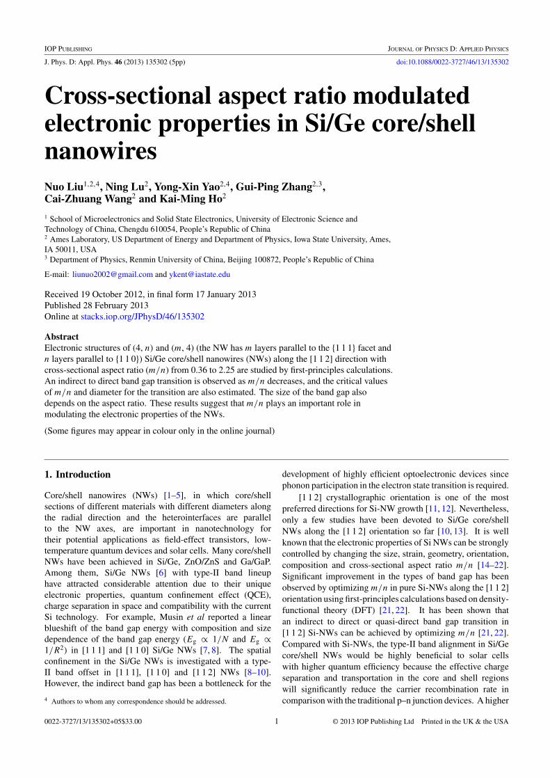
In the present DFT-LDA calculation, the rectangularhydrogen passivated Si/Ge core/shell NWs are constructedbased on the [1 1 2] Si NW structures found by experiments[26, 27] and by a global unbiased search with genetic algorithmin our previous works [28]. We denote the Si/Ge core/shell NWalong the [1 1 2] direction as (m, n) indicating that the NW hasm layers parallel to the {1 1 1} facet and n layers parallel to{1 1 0} facet that enclose the NW, as shown in figure 1. Theaxial lattice constants of the core/shell NWs are optimized byminimizing the total energy of the NWs with respect to theaxial lattice constants c while allowing all atoms in the NWsto relax by the conjugate-gradient method. The diameter forthe structures, which is defined as the largest distance betweentwo H atoms in the same cross-sectional plane of the NWs, islisted in table 1. To compare the electronic properties of theNWs with different m/n, we calculate the NWs of (4, n) and(m, 4) with m and n changing from 5 to 9. For the NWs studiedin this work, we found that the axial and radial expansion forthe (4, n) NWs is larger than that for the (m, 4) one whenm = n, although the total number of atoms in the unit cellof the two structures are the same, because interlayer distancebetween {1 1 1} facets is larger than that between {1 1 0} facets.
Figure 1. Perspective top view of (4, 8) (left) and (8, 4) (right)Si/Ge core/shell NWs with eight layers parallel to the {1 1 1} facetand four layers parallel to the {1 1 0} facet in the (8,4) NW.
3. Results and discussion
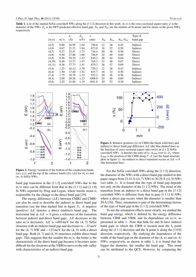
The variations of the top of the valence band and the bottom ofthe conduction band in (4, n) and (m, 4) Si/Ge NWs are shownin figure 2. Special attention is paid to the changes in bandstructure around the Fermi energy. Note that the m/n ratio forthe (4, n) core/shell NW is reciprocal to that of (n, 4). Thecharacteristics of the band structures of the core/shell NWs aredifferent from each other although the NWs are oriented alongthe same [1 1 2] direction. All (4, n) and (m, 4) NWs havetheir valence band maximum (VBM) at the � point (the centreof the Brillouin zone). However, the conduction band minima(CBM) of the NWs are located at several different positions.The CBM is located near the Z point (the boundary of theBrillouin zone) for the (m, 4) structures, making the bandgap indirect. This result indicates that the (m, 4) structuresare poor candidate for optoelectronic applications since theparticipation of phonons in the transition reduces the efficiencyof the devices. On the other hand, there are direct band gapsfor the (4, n) NWs with n > 6. There are two minima in theconduction band of the (4, n) NWs, one is located near theZ point (CBM1) and another at the � point (CBM2). With n
increasing from 5 to 9, CBM1 is raised in energy relative toCBM2. As a result, when n is larger than 6, CBM2 becomesthe global CBM, resulting in a direct band gap. Therefore, bychanging the aspect ratio m/n for (m, n) NWs, the indirect todirect band gap transition can be achieved.
Figure 3 shows the relative positions of the CBM atdifferent m/n ratios for the NWs (see the black dashed line),where�denotes the ratio of the distances k�–kCBM over k�–kZ .It is interesting to note that � becomes zero when m/n � 0.57and a direct band gap can be achieved for 0.36 < m/n � 0.57.Interestingly, the critical m/n ratio for the transition from anindirect to a direct gap in the [1 1 2] pure Si NWs [22] is0.5, which is smaller than the critical value of 0.57 for the[1 1 2] core/shell structures studied in this paper. This suggeststhat the Ge atoms in the shell region are helpful in increasingthe critical m/n ratio for direct band in the core. It is alsointeresting to note that the mechanism for the indirect to direct
2
J. Phys. D: Appl. Phys. 46 (2013) 135302 N Liu et al
Table 1. List of the studied Si/Ge core/shell NWs along the [1 1 2] direction in this work. m/n is the cross-sectional aspect ratio; d is thediameter of the NWs; Eg is the DFT predicted effective band gap; NSi and NGe are the number of Si atoms and Ge atoms in the given NWs,respectively.
d Eg λ Type of(m,n) m/n (Å) (eV) (nm) NSi NGe NSi/NGe band gap
(4,5) 0.80 16.99 1.64 756.0 12 28 0.43 Indirect(4,6) 0.67 21.23 1.84 673.8 16 32 0.50 Indirect(4,7) 0.57 23.41 1.73 716.4 20 36 0.56 Direct(4,8) 0.50 27.86 1.66‘ 746.9 24 40 0.60 Direct(4,9) 0.36 30.29 1.53 810.3 28 44 0.64 Direct(4,10) 0.40 33.37 1.47 765.3 32 48 0.67 Direct(4,11) 0.36 37.73 1.41 879.3 36 52 0.69 Direct(5,4) 1.25 16.12 1.70 729.3 12 28 0.43 Indirect(6,4) 1.50 17.40 1.52 815.7 16 32 0.50 Indirect(7,4) 1.75 18.79 1.33 932.2 20 36 0.56 Indirect(8,4) 2.00 20.26 1.23 1008.0 24 40 0.60 Indirect(9,4) 2.25 21.80 1.19 1041.8 20 52 0.38 Indirect
0.00 0.02 0.04 0.06 0.08-1.0
-0.8
-0.6
-0.4
-0.2(b)
Γ Γ Z
E (
eV
)
C
(4,5)
(4,6)
(4,7)
(4,8)
(4,9)
0.00 0.02 0.04 0.06 0.08
1.2
1.3
1.4
1.5
1.6
1.7
1.8
1.9
(a)
CMB1
E (
eV
)
∆E
CMB2
0.00 0.02 0.04 0.06 0.08
0.80.91.01.11.21.31.41.51.61.71.81.9
(c)CMB1
E (
eV
)
CMB2
0.00 0.02 0.04 0.06 0.08
-1.4
-1.2
-1.0
-0.8
-0.6
-0.4
-0.2
Z
(d )
E (
eV
)
(5,4)
(6,4)
(7,4)
(8,4)
(9,4)
Figure 2. Energy variation of the bottom of the conduction bands((a), (c)), and the top of the valence bands ((b), (d)) for (4, n) and(m, 4) Si/Ge NWs.
band gap transition in the [1 1 2] core/shell NWs due to them/n ratio can be different from that in the [1 1 1] and [1 1 0]Si NWs reported by Peng and Logan, where tensile strain isresponsible for the change to the direct band gap [29].
The energy difference (�E) between CMB2 and CMB1can also be used to describe the indirect to direct band gaptransition (see the blue dashed line in figure 3). A negative(positive) �E denotes a direct (indirect) band gap. Thehorizontal line at �E = 0 gives a reference of the transitionbetween indirect and direct band gaps. �E decreases as theratio m/n decreases; �E is +469 meV for the (4, 5) Si/Gestructure with an indirect band gap and decreases to −22 meVfor the (4, 7) NW and −122 meV for the (4, 9) with a directband gap. Both (4, 7) and (4, 9) structures exhibit direct bandgaps. This suggests that the smaller the m/n, the better is thecharacteristic of the direct band gap because it becomes moredifficult for the electrons at the VBM to move to the sub-valleywith characteristics of an indirect band gap.
0 1 2
0
50
100
m/n
∆ (
%)
-200
0
200
400
∆E
(me
V)
Figure 3. Relative position (�) of CBM (the black solid line) andindirect to direct band gap difference �E (the blue dashed line) asthe function of cross-sectional aspect ratio (m/n) in [1 1 2] Si/Gecore/shell NWs. � denotes the ratio of k�–kCBM over k�–kZ wherekCBM is the position of the CBM along �–Z (see the band structureplots in figure 1). An indirect to direct transition occurs at �E = 0(the horizontal line).
For the Si/Ge core/shell NWs along the [1 1 2] direction,the diameter of the NWs with a direct band gap studied in thispaper ranges from 23.41 Å ((4, 7) NW) to 30.29 Å ((4, 9) NW)(see table 1). It is found that the type of band gap dependsnot only on the diameter of the [1 1 2] NWs. The trend of thetransition from an indirect to a direct band gap in the [1 1 2]core/shell NWs is different from that in pure [1 1 1] Si NWswhere a direct gap occurs when the diameter is smaller than20 Å [30]. Thus, orientation is part of the determining factorsof the type of band gap in the [1 1 2] core/shell NWs.
To see the orientation effects more clearly, we studied theband gap energy, which is defined by the energy differencebetween CBM and VBM, and its dependence on m/n, aspresented in table 1. Note that bulk Ge and Si have indirectband gaps in which the CBM is located near the L pointalong the [1 1 1] direction and the X point is along the [1 0 0]direction, respectively. By studying the dependence of thewidth of the band gap on the diameter of the (4, n) and (m, 4)NWs, respectively, as shown in table 1, it is found that thebigger the diameter, the smaller the band gap. This trendcan be attributed to the QCE. However, by comparing the
3
J. Phys. D: Appl. Phys. 46 (2013) 135302 N Liu et al
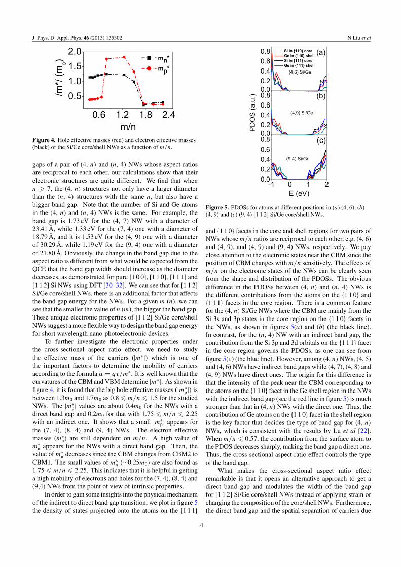
Figure 4. Hole effective masses (red) and electron effective masses(black) of the Si/Ge core/shell NWs as a function of m/n.
gaps of a pair of (4, n) and (n, 4) NWs whose aspect ratiosare reciprocal to each other, our calculations show that theirelectronic structures are quite different. We find that whenn � 7, the (4, n) structures not only have a larger diameterthan the (n, 4) structures with the same n, but also have abigger band gap. Note that the number of Si and Ge atomsin the (4, n) and (n, 4) NWs is the same. For example, theband gap is 1.73 eV for the (4, 7) NW with a diameter of23.41 Å, while 1.33 eV for the (7, 4) one with a diameter of18.79 Å, and it is 1.53 eV for the (4, 9) one with a diameterof 30.29 Å, while 1.19 eV for the (9, 4) one with a diameterof 21.80 Å. Obviously, the change in the band gap due to theaspect ratio is different from what would be expected from theQCE that the band gap width should increase as the diameterdecreases, as demonstrated for pure [1 0 0], [1 1 0], [1 1 1] and[1 1 2] Si NWs using DFT [30–32]. We can see that for [1 1 2]Si/Ge core/shell NWs, there is an additional factor that affectsthe band gap energy for the NWs. For a given m (n), we cansee that the smaller the value of n (m), the bigger the band gap.These unique electronic properties of [1 1 2] Si/Ge core/shellNWs suggest a more flexible way to design the band gap energyfor short wavelength nano-photoelectronic devices.
To further investigate the electronic properties underthe cross-sectional aspect ratio effect, we need to studythe effective mass of the carriers (|m∗|) which is one ofthe important factors to determine the mobility of carriersaccording to the formula µ = qτ/m∗. It is well known that thecurvatures of the CBM and VBM determine |m∗|. As shown infigure 4, it is found that the big hole effective masses (|m∗
p|) isbetween 1.3m0 and 1.7m0 as 0.8 � m/n � 1.5 for the studiedNWs. The |m∗
p| values are about 0.4m0 for the NWs with adirect band gap and 0.2m0 for that with 1.75 � m/n � 2.25with an indirect one. It shows that a small |m∗
p| appears forthe (7, 4), (8, 4) and (9, 4) NWs. The electron effectivemasses (m∗
n) are still dependent on m/n. A high value ofm∗
n appears for the NWs with a direct band gap. Then, thevalue of m∗
n decreases since the CBM changes from CBM2 toCBM1. The small values of m∗
n (∼0.25m0) are also found as1.75 � m/n � 2.25. This indicates that it is helpful in gettinga high mobility of electrons and holes for the (7, 4), (8, 4) and(9,4) NWs from the point of view of intrinsic properties.
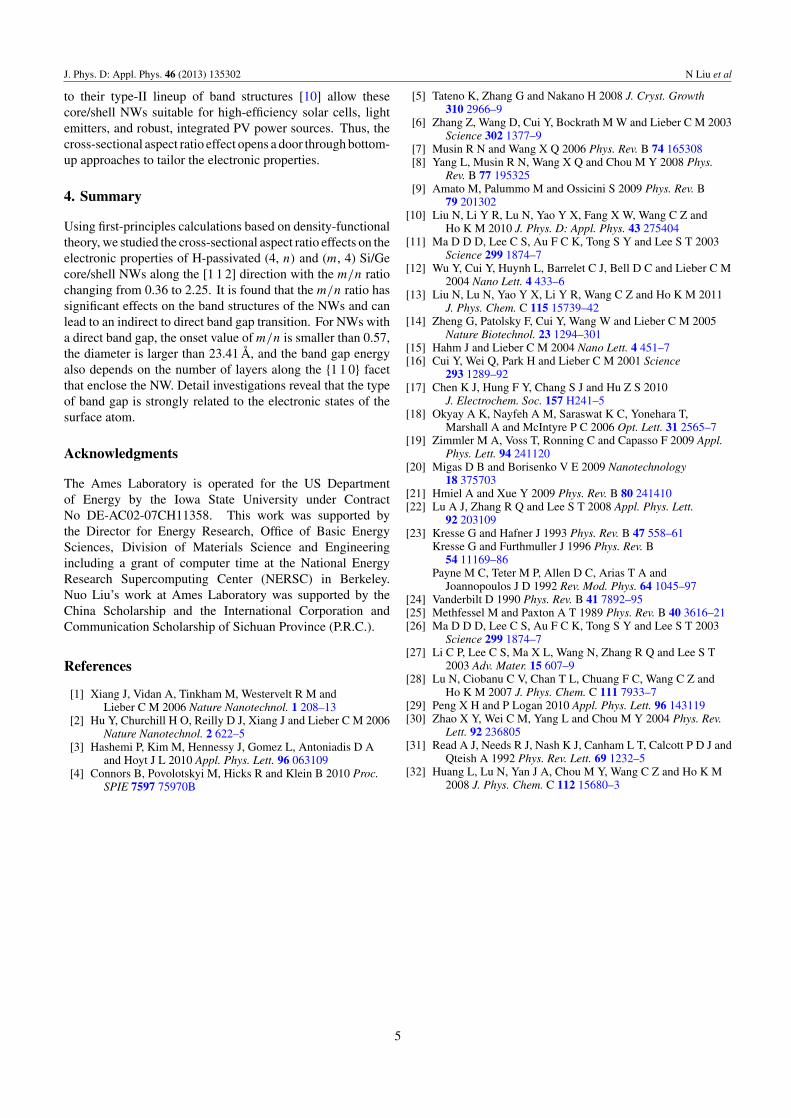
In order to gain some insights into the physical mechanismof the indirect to direct band gap transition, we plot in figure 5the density of states projected onto the atoms on the {1 1 1}
-1 0 1 20.0
0.2
0.4
0.6
0.8
E (eV)
(c)
(9,4) Si/Ge
-1 0 1 2
0.0
0.2
0.4
0.6
0.8 (a)
(4,6) Si/Ge
Si in {110} core
Ge in {110} shell
Si in {111} core
Ge in {111} shell
-1 0 1 2
0.0
0.2
0.4
0.6
0.8 (b)
(4,9) Si/Ge
PD
OS
(a.u
.)
Figure 5. PDOSs for atoms at different positions in (a) (4, 6), (b)(4, 9) and (c) (9, 4) [1 1 2] Si/Ge core/shell NWs.
and {1 1 0} facets in the core and shell regions for two pairs ofNWs whose m/n ratios are reciprocal to each other, e.g. (4, 6)and (4, 9), and (4, 9) and (9, 4) NWs, respectively. We payclose attention to the electronic states near the CBM since theposition of CBM changes with m/n sensitively. The effects ofm/n on the electronic states of the NWs can be clearly seenfrom the shape and distribution of the PDOSs. The obviousdifference in the PDOSs between (4, n) and (n, 4) NWs isthe different contributions from the atoms on the {1 1 0} and{1 1 1} facets in the core region. There is a common featurefor the (4, n) Si/Ge NWs where the CBM are mainly from theSi 3s and 3p states in the core region on the {1 1 0} facets inthe NWs, as shown in figures 5(a) and (b) (the black line).In contrast, for the (n, 4) NW with an indirect band gap, thecontribution from the Si 3p and 3d orbitals on the {1 1 1} facetin the core region governs the PDOSs, as one can see fromfigure 5(c) (the blue line). However, among (4, n) NWs, (4, 5)and (4, 6) NWs have indirect band gaps while (4, 7), (4, 8) and(4, 9) NWs have direct ones. The origin for this difference isthat the intensity of the peak near the CBM corresponding tothe atoms on the {1 1 0} facet in the Ge shell region in the NWswith the indirect band gap (see the red line in figure 5) is muchstronger than that in (4, n) NWs with the direct one. Thus, thecontribution of Ge atoms on the {1 1 0} facet in the shell regionis the key factor that decides the type of band gap for (4, n)
NWs, which is consistent with the results by Lu et al [22].When m/n � 0.57, the contribution from the surface atom tothe PDOS decreases sharply, making the band gap a direct one.Thus, the cross-sectional aspect ratio effect controls the typeof the band gap.
What makes the cross-sectional aspect ratio effectremarkable is that it opens an alternative approach to get adirect band gap and modulates the width of the band gapfor [1 1 2] Si/Ge core/shell NWs instead of applying strain orchanging the composition of the core/shell NWs. Furthermore,the direct band gap and the spatial separation of carriers due
4
J. Phys. D: Appl. Phys. 46 (2013) 135302 N Liu et al
to their type-II lineup of band structures [10] allow thesecore/shell NWs suitable for high-efficiency solar cells, lightemitters, and robust, integrated PV power sources. Thus, thecross-sectional aspect ratio effect opens a door through bottom-up approaches to tailor the electronic properties.
4. Summary
Using first-principles calculations based on density-functionaltheory, we studied the cross-sectional aspect ratio effects on theelectronic properties of H-passivated (4, n) and (m, 4) Si/Gecore/shell NWs along the [1 1 2] direction with the m/n ratiochanging from 0.36 to 2.25. It is found that the m/n ratio hassignificant effects on the band structures of the NWs and canlead to an indirect to direct band gap transition. For NWs witha direct band gap, the onset value of m/n is smaller than 0.57,the diameter is larger than 23.41 Å, and the band gap energyalso depends on the number of layers along the {1 1 0} facetthat enclose the NW. Detail investigations reveal that the typeof band gap is strongly related to the electronic states of thesurface atom.
Acknowledgments
The Ames Laboratory is operated for the US Departmentof Energy by the Iowa State University under ContractNo DE-AC02-07CH11358. This work was supported bythe Director for Energy Research, Office of Basic EnergySciences, Division of Materials Science and Engineeringincluding a grant of computer time at the National EnergyResearch Supercomputing Center (NERSC) in Berkeley.Nuo Liu’s work at Ames Laboratory was supported by theChina Scholarship and the International Corporation andCommunication Scholarship of Sichuan Province (P.R.C.).
References
[1] Xiang J, Vidan A, Tinkham M, Westervelt R M andLieber C M 2006 Nature Nanotechnol. 1 208–13
[2] Hu Y, Churchill H O, Reilly D J, Xiang J and Lieber C M 2006Nature Nanotechnol. 2 622–5
[3] Hashemi P, Kim M, Hennessy J, Gomez L, Antoniadis D Aand Hoyt J L 2010 Appl. Phys. Lett. 96 063109
[4] Connors B, Povolotskyi M, Hicks R and Klein B 2010 Proc.SPIE 7597 75970B
[5] Tateno K, Zhang G and Nakano H 2008 J. Cryst. Growth310 2966–9
[6] Zhang Z, Wang D, Cui Y, Bockrath M W and Lieber C M 2003Science 302 1377–9
[7] Musin R N and Wang X Q 2006 Phys. Rev. B 74 165308[8] Yang L, Musin R N, Wang X Q and Chou M Y 2008 Phys.
Rev. B 77 195325[9] Amato M, Palummo M and Ossicini S 2009 Phys. Rev. B
79 201302[10] Liu N, Li Y R, Lu N, Yao Y X, Fang X W, Wang C Z and
Ho K M 2010 J. Phys. D: Appl. Phys. 43 275404[11] Ma D D D, Lee C S, Au F C K, Tong S Y and Lee S T 2003
Science 299 1874–7[12] Wu Y, Cui Y, Huynh L, Barrelet C J, Bell D C and Lieber C M
2004 Nano Lett. 4 433–6[13] Liu N, Lu N, Yao Y X, Li Y R, Wang C Z and Ho K M 2011
J. Phys. Chem. C 115 15739–42[14] Zheng G, Patolsky F, Cui Y, Wang W and Lieber C M 2005
Nature Biotechnol. 23 1294–301[15] Hahm J and Lieber C M 2004 Nano Lett. 4 451–7[16] Cui Y, Wei Q, Park H and Lieber C M 2001 Science
293 1289–92[17] Chen K J, Hung F Y, Chang S J and Hu Z S 2010
J. Electrochem. Soc. 157 H241–5[18] Okyay A K, Nayfeh A M, Saraswat K C, Yonehara T,
Marshall A and McIntyre P C 2006 Opt. Lett. 31 2565–7[19] Zimmler M A, Voss T, Ronning C and Capasso F 2009 Appl.
Phys. Lett. 94 241120[20] Migas D B and Borisenko V E 2009 Nanotechnology
18 375703[21] Hmiel A and Xue Y 2009 Phys. Rev. B 80 241410[22] Lu A J, Zhang R Q and Lee S T 2008 Appl. Phys. Lett.
92 203109[23] Kresse G and Hafner J 1993 Phys. Rev. B 47 558–61
Kresse G and Furthmuller J 1996 Phys. Rev. B54 11169–86
Payne M C, Teter M P, Allen D C, Arias T A andJoannopoulos J D 1992 Rev. Mod. Phys. 64 1045–97
[24] Vanderbilt D 1990 Phys. Rev. B 41 7892–95[25] Methfessel M and Paxton A T 1989 Phys. Rev. B 40 3616–21[26] Ma D D D, Lee C S, Au F C K, Tong S Y and Lee S T 2003
Science 299 1874–7[27] Li C P, Lee C S, Ma X L, Wang N, Zhang R Q and Lee S T
2003 Adv. Mater. 15 607–9[28] Lu N, Ciobanu C V, Chan T L, Chuang F C, Wang C Z and
Ho K M 2007 J. Phys. Chem. C 111 7933–7[29] Peng X H and P Logan 2010 Appl. Phys. Lett. 96 143119[30] Zhao X Y, Wei C M, Yang L and Chou M Y 2004 Phys. Rev.
Lett. 92 236805[31] Read A J, Needs R J, Nash K J, Canham L T, Calcott P D J and
Qteish A 1992 Phys. Rev. Lett. 69 1232–5[32] Huang L, Lu N, Yan J A, Chou M Y, Wang C Z and Ho K M
2008 J. Phys. Chem. C 112 15680–3
5


![119 Nanowires 4. Nanowires - UFAMhome.ufam.edu.br/berti/nanomateriais/Nanowires.pdf · 119 Nanowires 4. Nanowires ... written about carbon nanotubes [4.57–59], which can be](https://img.pdfslide.us/doc/110x75/5abfd11e7f8b9a5d718eba2b/119-nanowires-4-nanowires-nanowires-4-nanowires-written-about-carbon-nanotubes.jpg)

![Spin configuration in isolated FeCoCu nanowires modulated ... · nanostrips fabricated by nanolithography, DWs are arti ficially pinned by notches or local stray fields [8] but](https://img.pdfslide.us/doc/110x75/5d6231a188c993284d8b808c/spin-configuration-in-isolated-fecocu-nanowires-modulated-nanostrips-fabricated.jpg)