Embed Size (px)
Citation preview
101 Innovation DriveSan Jose, CA 95134www.altera.com
Creating Multiprocessor Nios II SystemsTutorial
Document Version: 1.4Document Date: February 2010
TU-N2033005-1.4

Copyright © 2010 Altera Corporation. All rights reserved. Altera, The Programmable Solutions Company, the stylized Altera logo, specific device designations, and all otherwords and logos that are identified as trademarks and/or service marks are, unless noted otherwise, the trademarks and service marks of Altera Corporation in the U.S. and othercountries. All other product or service names are the property of their respective holders. Altera products are protected under numerous U.S. and foreign patents and pending ap-plications, maskwork rights, and copyrights. Altera warrants performance of its semiconductor products to current specifications in accordance with Altera's standard warranty,but reserves the right to make changes to any products and services at any time without notice. Altera assumes no responsibility or liability arising out of the application or use ofany information, product, or service described herein except as expressly agreed to in writing by Altera Corporation. Altera customers are advised to obtain the latest version ofdevice specifications before relying on any published information and before placing orders for products or services.
© February 2010 Altera Corporation
Contents
Chapter 1. Creating Multiprocessor Nios II SystemsIntroduction . . . . . . . . . . . . . . . . . . . . . . . . . . . . . . . . . . . . . . . . . . . . . . . . . . . . . . . . . . . . . . . . . . . . . . . . . . . . 1-1Benefits of Multiprocessor Systems . . . . . . . . . . . . . . . . . . . . . . . . . . . . . . . . . . . . . . . . . . . . . . . . . . . . . . . 1-2Nios II Multiprocessor Systems . . . . . . . . . . . . . . . . . . . . . . . . . . . . . . . . . . . . . . . . . . . . . . . . . . . . . . . . . . . 1-2Hardware Design Considerations . . . . . . . . . . . . . . . . . . . . . . . . . . . . . . . . . . . . . . . . . . . . . . . . . . . . . . . . . 1-3
Autonomous Multiprocessors . . . . . . . . . . . . . . . . . . . . . . . . . . . . . . . . . . . . . . . . . . . . . . . . . . . . . . . . . . 1-3Multiprocessors that Share Resources . . . . . . . . . . . . . . . . . . . . . . . . . . . . . . . . . . . . . . . . . . . . . . . . . . 1-4
Sharing Resources in a Multiprocessor System . . . . . . . . . . . . . . . . . . . . . . . . . . . . . . . . . . . . . . . . . . . . . 1-4Sharing Memory . . . . . . . . . . . . . . . . . . . . . . . . . . . . . . . . . . . . . . . . . . . . . . . . . . . . . . . . . . . . . . . . . . . . . 1-6The Hardware Mutex and Mailbox Cores . . . . . . . . . . . . . . . . . . . . . . . . . . . . . . . . . . . . . . . . . . . . . . . 1-7Sharing Peripherals Between Multiple Processors . . . . . . . . . . . . . . . . . . . . . . . . . . . . . . . . . . . . . . . . 1-8Multiprocessors and Overlapping Address Space . . . . . . . . . . . . . . . . . . . . . . . . . . . . . . . . . . . . . . . . 1-9
Software Design Considerations . . . . . . . . . . . . . . . . . . . . . . . . . . . . . . . . . . . . . . . . . . . . . . . . . . . . . . . . . 1-10Program Memory . . . . . . . . . . . . . . . . . . . . . . . . . . . . . . . . . . . . . . . . . . . . . . . . . . . . . . . . . . . . . . . . . . . . 1-10Boot Addresses . . . . . . . . . . . . . . . . . . . . . . . . . . . . . . . . . . . . . . . . . . . . . . . . . . . . . . . . . . . . . . . . . . . . . . 1-12Running and Debugging Multiprocessor Systems from the Nios II SBT for Eclipse . . . . . . . . . 1-14
Design Example . . . . . . . . . . . . . . . . . . . . . . . . . . . . . . . . . . . . . . . . . . . . . . . . . . . . . . . . . . . . . . . . . . . . . . . 1-15Hardware and Software Requirements . . . . . . . . . . . . . . . . . . . . . . . . . . . . . . . . . . . . . . . . . . . . . . . . . 1-15Installation Notes . . . . . . . . . . . . . . . . . . . . . . . . . . . . . . . . . . . . . . . . . . . . . . . . . . . . . . . . . . . . . . . . . . . . 1-15Creating the Hardware System . . . . . . . . . . . . . . . . . . . . . . . . . . . . . . . . . . . . . . . . . . . . . . . . . . . . . . . . 1-15
Creating Software for the Multiprocessor System . . . . . . . . . . . . . . . . . . . . . . . . . . . . . . . . . . . . . . . . . . 1-24Building the Application and BSP Projects . . . . . . . . . . . . . . . . . . . . . . . . . . . . . . . . . . . . . . . . . . . . . 1-24Starting the Nios II SBT for Eclipse . . . . . . . . . . . . . . . . . . . . . . . . . . . . . . . . . . . . . . . . . . . . . . . . . . . . 1-25Importing the Software Projects . . . . . . . . . . . . . . . . . . . . . . . . . . . . . . . . . . . . . . . . . . . . . . . . . . . . . . . 1-25Building the Software Projects . . . . . . . . . . . . . . . . . . . . . . . . . . . . . . . . . . . . . . . . . . . . . . . . . . . . . . . . 1-26Creating a Debug Configuration for Each Processor . . . . . . . . . . . . . . . . . . . . . . . . . . . . . . . . . . . . . 1-26Debugging the Software Projects on the Board . . . . . . . . . . . . . . . . . . . . . . . . . . . . . . . . . . . . . . . . . . 1-27
Conclusion . . . . . . . . . . . . . . . . . . . . . . . . . . . . . . . . . . . . . . . . . . . . . . . . . . . . . . . . . . . . . . . . . . . . . . . . . . . . 1-27
Additional InformationRevision History . . . . . . . . . . . . . . . . . . . . . . . . . . . . . . . . . . . . . . . . . . . . . . . . . . . . . . . . . . . . . . . . . . . . . Info-1Referenced Documents . . . . . . . . . . . . . . . . . . . . . . . . . . . . . . . . . . . . . . . . . . . . . . . . . . . . . . . . . . . . . . . Info-1How to Contact Altera . . . . . . . . . . . . . . . . . . . . . . . . . . . . . . . . . . . . . . . . . . . . . . . . . . . . . . . . . . . . . . . . Info-1Typographic Conventions . . . . . . . . . . . . . . . . . . . . . . . . . . . . . . . . . . . . . . . . . . . . . . . . . . . . . . . . . . . . Info-2
Creating Multiprocessor Nios II Systems Tutorial

iv
Creating Multiprocessor Nios II Systems Tutorial © February 2010 Altera Corporation
© February 2010 Altera Corporation
1. Creating Multiprocessor Nios IISystems
This tutorialdescribes thefeaturesof theAltera® Nios® IIprocessorandSOPCBuildertool that are useful for creating systems with two or more processors. The tutorialprovides an example design that guides you through a step-by-step process forbuilding a multiprocessor system containing two processors that access a sharedmemory buffer using a mailbox. It shows you how to use the Nios II Software BuildTools (SBT) for Eclipse to create and debug two software projects, one for eachprocessor in the system.
f Refer to the Nios II Embedded Design Suite Release Notes and Errata and the MegaCore IPLibrary Release Notes and Errata for the latest features, enhancements, and knownissues in the current release.
IntroductionAny system that incorporates two or more microprocessors working together toperform one or more related tasks is commonly referred to as a multiprocessorsystem. Developers using the Altera Nios II processor and SOPC Builder tool canquickly design and build multiprocessor systems that share resources. SOPC Builderis a system development tool for creating SOPC design systems that can includeprocessors, peripherals, and memories. A Nios II processor system typically refers toa system with a processor core, a set of on-chip peripherals, on-chip memory andinterfaces to off-chip memory all implemented on a single Altera device.
This document describes the features of the Nios II processor and SOPC Builder toolthat are useful for creating systems with two or more processors. This documentprovides an example design that guides you through a step-by-step process forbuilding a multiprocessor system containing two processors that share a mail box anda memory buffer. Using the Nios II SBT, you create two software projects, one for eachprocessor in the system. Then you import these two software projects to the Nios IISBT for Eclipse, and use the Nios II SBT for Eclipse to debug these two softwareprojects.
After completing this document, you will have the knowledge to perform thefollowing tasks:
■ Build an SOPC Builder system containing more than one Nios II processor.
■ Safely share resources between processors, avoiding data corruption.
■ Build software projects for multiprocessor systems using the Nios II SBT.
■ DebugmultiplesoftwareprojectsrunningonmultipleprocessorsusingtheNios IISBT for Eclipse.
This chapter assumes that you are familiar with reading and writing embeddedsoftware and that you have read and followed the step-by-step procedures forbuilding a microprocessor system in the Nios II Hardware Development Tutorial.
f The Nios II Hardware Development Tutorial can be found on the Literature: Nios IIProcessor page.
Creating Multiprocessor Nios II Systems TutorialPreliminary
Chapter 1: Creating Multiprocessor Nios II Systems 1–2Benefits of Multiprocessor Systems
Benefits of Multiprocessor SystemsMultiprocessor systems possess the benefit of increased performance, but nearlyalways at the price of significantly increased system complexity. For this reason, theuse of multiprocessor systems has historically been limited to workstation andhigh-end PC computing using a complex method of load-sharing often referred to assymmetric multiprocessing (SMP). While the overhead of SMP is typically too highfor most embedded systems, the idea of using multiple processors to performdifferent tasks and functions on different processors in embedded applications(asymmetrical) is gaining popularity. Altera FPGAs provide an ideal platform fordevelopingasymmetricembeddedmultiprocessorsystems,becausethehardwarecaneasily be modified and tuned using the SOPC Builder tool to provide optimal systemperformance. Recent increases in the size of Altera FPGAs make possible systemdesigns with many Nios II processors on a single chip. Furthermore, with a powerfulintegration tool like SOPC Builder, different system configurations can be designed,built, and evaluated very quickly.
Nios II Multiprocessor SystemsThe Nios II SBT for Eclipse includes features to help with the creation and debuggingof multiprocessor systems. Multiple Nios II processors are able to efficiently sharesystemresourcesthankstothemultimasterfriendlyslave-sidearbitrationcapabilitiesof the system interconnect fabric. Since the capabilities of SOPC Builder now allowusers to almost effortlessly add as many processors to a system as desired, the designfocus in building multiprocessor systems no longer lies in the arranging andconnecting of hardware components. The challenge in building multiprocessorsystems now lies in writing the software for those processors so they operateefficiently together, and do not conflict with one another.
To aid in the prevention of multiple processors interfering with each other,multiprocessor coordination peripherals, such as a hardware mutex core and ahardware mailbox core, are included in the Nios II Embedded Design Suite (EDS).The hardware mutex core allows different processors to claim ownership of a sharedresource for a period of time. This temporary ownership of a resource by a processorprotects the shared resource from corruption by the actions of another processor.
To prevent corruption, you must write software that waits to acquire the mutex beforeit accesses the shared resource, ensuring mutually exclusive access. An atomictest-and-set operation, which cannot be interrupted, allows a processor to check forownership and acquire ownership in a single operation, avoiding the potential pitfallof two processors each confirming that no processor currently has ownership,followed by both processors acquiring the resource, violating mutual exclusion. Thefact that the operation cannot be interrupted also ensures that an operating systemtask switch cannot occur while the processor is acquiring or releasing the mutex.
The hardware mutex core provides a semaphore for mutually exclusive access to anyresource. The software determines that resource and is responsible for using themutex core to ensure mutually exclusive access.
© February 2010 Altera Corporation Creating Multiprocessor Nios II Systems TutorialPreliminary
Chapter 1: Creating Multiprocessor Nios II Systems 1–3Hardware Design Considerations
The hardware mailbox core allows different processors to coordinate with each otherby providing both mutually exclusive access and data exchange in a single resource.The mailbox hardware core implementation includes the functionality of two mutexcores, one to guarantee mutually exclusive access for reading from the mailbox andone to guarantee mutually exclusive access for writing to the mailbox.
For more information about mutually exclusive access to shared memory, refer to“The Hardware Mutex and Mailbox Cores” on page 1–7.
The Nios II SBT for Eclipse supports software debug on multiprocessor systems, byallowing users to launch and stop software debug sessions on simultaneouslyrunning processors.
Hardware Design ConsiderationsNios II multiprocessor systems are split into two main categories, those that shareresources, and those in which each processor is autonomous and does not shareresources with other processors.
Autonomous MultiprocessorsWhile autonomous multiprocessor systems contain multiple processors, theseprocessors are completely autonomous and do not communicate with the others,much as if they were completely separate systems. Systems of this type are typicallyless complicated and pose fewer challenges because by design, they do not shareresourcesandsothesystem'sprocessorsare incapableof interferingwitheachother'soperation. Figure 1–1 shows a block diagram of two autonomous processors in amultiprocessor system.
© February 2010 Altera Corporation Creating Multiprocessor Nios II Systems TutorialPreliminary

Chapter 1: Creating Multiprocessor Nios II Systems 1–4Sharing Resources in a Multiprocessor System
Multiprocessors that Share ResourcesMultiprocessor systems that share resources can pose many more challenges. Whilethe Nios II EDS includes features making it possible to reliably implementmultiprocessor systems that share resources, the creation of such systems is notnecessarily a straightforward venture. Altera recommends that you complete thistutorial and fully understand its recommendations before attempting to create aresource-sharing multiprocessor system.
Sharing Resources in a Multiprocessor SystemResources are considered shared when they are available to be accessed by more thanone processor. The SOPC Builder connections panel controls which hardwarecomponents can be accessed by each individual Nios II processor.
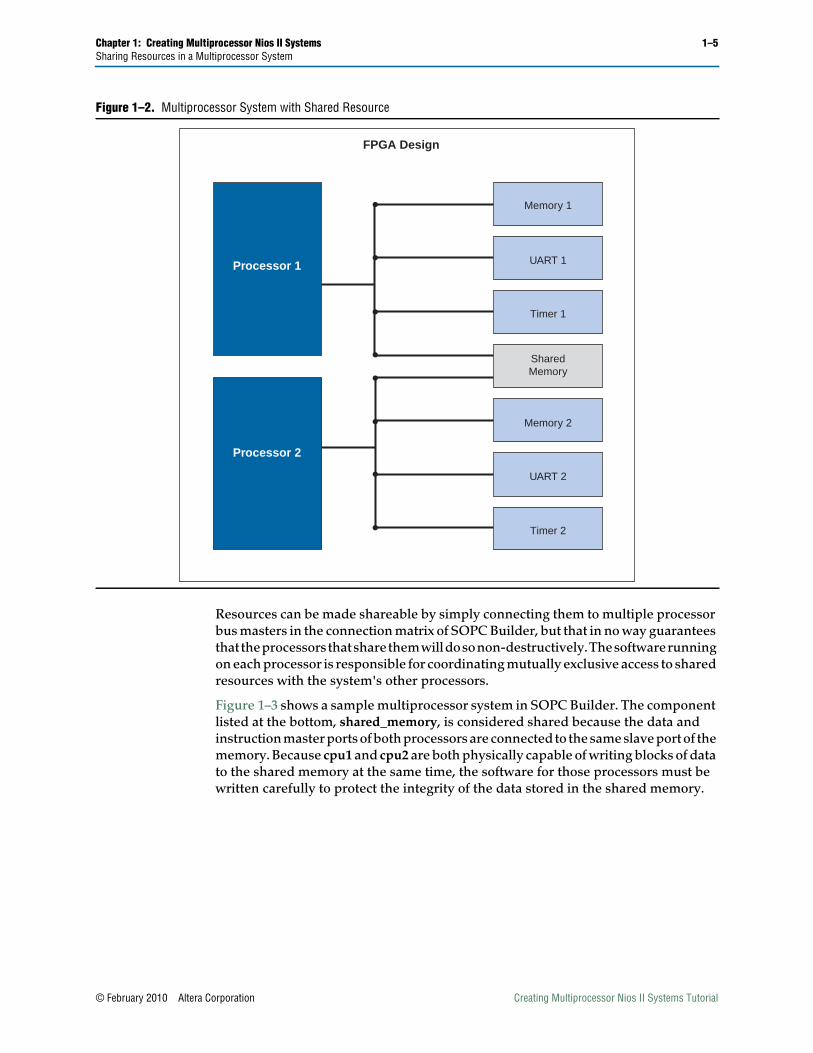
Shared resources can be a very powerful aspect of multiprocessor systems, but caremust be taken when deciding which system resources are shared, and how thedifferent processors will cooperate regarding the use of resources. Figure 1–2 shows ablock diagram of a sample multiprocessor system in which two processors share anon-chip memory.
Figure 1–1. Autonomous Multiprocessor System
Processor 1
Processor 2
Memory 1
UART 1
Timer 1
Memory 2
UART 2
Timer 2
© February 2010 Altera Corporation Creating Multiprocessor Nios II Systems TutorialPreliminary
Chapter 1: Creating Multiprocessor Nios II Systems 1–5Sharing Resources in a Multiprocessor System
Resources can be made shareable by simply connecting them to multiple processorbus masters in the connection matrix of SOPC Builder, but that in no way guaranteesthat theprocessorsthatsharethemwilldosonon-destructively.Thesoftwarerunningon each processor is responsible for coordinating mutually exclusive access to sharedresources with the system's other processors.
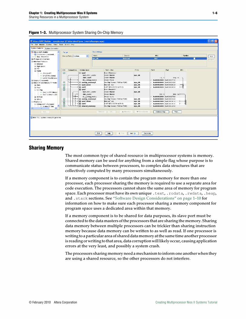
Figure 1–3 shows a sample multiprocessor system in SOPC Builder. The componentlisted at the bottom, shared_memory, is considered shared because the data andinstruction master ports of both processors are connected to the same slave port of thememory. Because cpu1 and cpu2 are both physically capable of writing blocks of datato the shared memory at the same time, the software for those processors must bewritten carefully to protect the integrity of the data stored in the shared memory.
Figure 1–2. Multiprocessor System with Shared Resource
FPGA Design
Processor 1
Memory 1
Processor 2
Timer 2
UART 2
Memory 2
SharedMemory
Timer 1
UART 1
© February 2010 Altera Corporation Creating Multiprocessor Nios II Systems TutorialPreliminary
Chapter 1: Creating Multiprocessor Nios II Systems 1–6Sharing Resources in a Multiprocessor System
Sharing MemoryThe most common type of shared resource in multiprocessor systems is memory.Shared memory can be used for anything from a simple flag whose purpose is tocommunicate status between processors, to complex data structures that arecollectively computed by many processors simultaneously.
If a memory component is to contain the program memory for more than oneprocessor, each processor sharing the memory is required to use a separate area forcode execution. The processors cannot share the same area of memory for programspace. Each processor must have its own unique .text, .rodata, .rwdata, .heap,and .stack sections. See “Software Design Considerations” on page 1–10 forinformation on how to make sure each processor sharing a memory component forprogram space uses a dedicated area within that memory.
If a memory component is to be shared for data purposes, its slave port must beconnected to the data masters of the processors that are sharing the memory. Sharingdata memory between multiple processors can be trickier than sharing instructionmemory because data memory can be written to as well as read. If one processor iswriting to a particular area of shared data memory at the same time another processoris reading or writing to that area, data corruption will likely occur, causing applicationerrors at the very least, and possibly a system crash.
The processors sharing memory need a mechanism to inform one another when theyare using a shared resource, so the other processors do not interfere.
Figure 1–3. Multiprocessor System Sharing On-Chip Memory
© February 2010 Altera Corporation Creating Multiprocessor Nios II Systems TutorialPreliminary
Chapter 1: Creating Multiprocessor Nios II Systems 1–7Sharing Resources in a Multiprocessor System
The Hardware Mutex and Mailbox CoresThe Nios II processor provides protection of shared resources with its hardwaremutex and mailbox core features. The hardware mutex and mailbox cores are notinternal features of the Nios II processor; they are small SOPC Builder components.
The term mutex stands for mutual exclusion, and a mutex does exactly as its namesuggests. A mutex allows cooperating processors to agree that one of them should beallowed mutually exclusive access to a hardware resource in the system. This is usefulfor the purpose of protecting resources from data corruption that can occur if morethan one processor attempts to use the resource at the same time.
The mutex core acts as a shared resource, providing an atomic test-and-set operationthat allows a processor to test if the mutex is available and if so, to acquire the mutexlock in a single operation. When the processor is finished using the shared resourceassociated with the mutex, the processor releases the mutex lock. Now anotherprocessor may acquire the mutex lock and use the shared resource. Without themutex, this kind of function would normally require the processor to execute twoseparateinstructions, testandset,betweenwhichanotherprocessorcouldalsotest foravailability and succeed. This situation would leave two processors both thinkingthey successfully acquired mutually exclusive access to the shared resource whenclearly they did not.
It is important to note that the mutex core does not physically protect resources in thesystem from being accessed at the same time by multiple processors. The softwarerunning on the processors is responsible for abiding by the rules. The software mustbe designed to always acquire the mutex before accessing its associated sharedresource.
f For more information about the hardware mutex core, refer to the Mutex Core chapterin Volume 5: Embedded Peripherals of the Quartus II Handbook.
The mailbox core provides safe access to the shared memory location of the mailboxmessages, but only if all accesses to this shared memory are performed using thehardware mailbox core’s software API. Physically, as seen in the SOPC Builderconnections panel, multiple processors are connected to the shared memory throughtheir data master ports, and in theory any one of them could simply write to theshared memory, violating mutual exclusion and overwriting data. However, if themailbox core uses a dedicated shared memory, as in the design example for thistutorial, and all accesses to that shared memory are handled through the API,mutually exclusive access is ensured. Each hardware mailbox core you implement inyour SOPC Builder system is associated with a specific shared memory.
The mailbox hardware core implementation includes the functionality of two mutexcores, one to guarantee mutually exclusive access for reading from the mailbox andone to guarantee mutually exclusive access for writing to the mailbox. Manipulationof mutex acquisition and relinquishing is handled through the API. The mailboxoperations visible to the software are altera_avalon_mailbox_pend(),altera_avalon_mailbox_post(), and a non-blocking get operation.
f For more information about the hardware mailbox core, refer to the Mailbox Corechapter in Volume 5: Embedded Peripherals of the Quartus II Handbook.
© February 2010 Altera Corporation Creating Multiprocessor Nios II Systems TutorialPreliminary

Chapter 1: Creating Multiprocessor Nios II Systems 1–8Sharing Resources in a Multiprocessor System
Another kind of mutex, called a software mutex, is common in many operatingsystems for providing the same protection of resources. The difference is that asoftware mutex is purely a software construct that is used to protect hardwareresourcesfrombeingcorruptedbymultipleprocessesrunningonthesameprocessor.A hardware mutex core is an SOPC Builder component with an Avalon interface thatuses logic to guarantee only one processor is granted the lock of the mutex at anygiven time. Similarly, a hardware mailbox core in an SOPC Builder system guaranteesonly one processor acquires the mailbox-associated mutex for writing at any giventime, and that only one processor acquires the mailbox-associated mutex for readingat any given time. If every processor waits until it acquires the appropriate mutexbefore using the associated shared resource, the resource is protected from potentialcorruption caused by simultaneous access by multiple processors. In the case of thehardware mailbox core, the API call tells the mailbox to acquire the mutex on behalf ofthe processor. In the case of the hardware mutex core, each Nios II processor mustacquire and relinquish the mutex from the mutex core directly. The hardware mutexcore itself has no connection to the shared resource; it merely provides a semaphore.Software must be written so that no processor attempts to access the shared resourcewithout first acquiring the mutex.
In some limited cases a mutex core or mailbox core might not be necessary. Such casesmight include one-way or circular message buffer arrangements in which only oneprocessor ever writes to a particular set of memory locations. However, sharingresources safely without a mutex core or mailbox core can be complicated. When indoubt, use the mutex core or the mailbox core.
Sharing Peripherals Between Multiple ProcessorsIn general, with the exception of the mutex core and the mailbox core, the Nios II EDSdoes not support sharing non-memory peripherals between multiple processors.
Sharingperipheralsinmultiprocessorsystemspresentssomedifficultchallenges,andis generally considered to lead to inefficient system designs. The biggest problemsarise for peripherals with interrupts. If a peripheral is allowed to interrupt all theprocessors that share it, there is no reliable way to guarantee which processor willrespond first and service that interrupt. Additionally, if the peripheral is used as aninput device for multiple processors, it becomes difficult to determine whichprocessor is supposed to collect given input from the device. While it is conceivablethat a complex system of handshaking could be created to handle these scenarios,such a system is beyond the scope of this document, and is unsupported by theNios II hardware abstraction layer (HAL) library.
f For more information about the Nios II HAL Library, refer to the Nios II SoftwareDeveloper's Handbook.
Memoryperipheralsandmultiprocessorcoordinationperipheralscanbeaccessedbymultiple processors. Altera recommends that you restrict all other peripherals to beaccessible by only one processor in the system. If other processors require use of theperipheral, they should use a hardware mailbox, or a message buffer that ismutex-protected or otherwise multiprocessor-safe, to communicate with the singleprocessor that is connected to that peripheral.
© February 2010 Altera Corporation Creating Multiprocessor Nios II Systems TutorialPreliminary

Chapter 1: Creating Multiprocessor Nios II Systems 1–9Sharing Resources in a Multiprocessor System
When building any system, especially a multiprocessor system, it is advisable to onlymake connections between peripherals that require communication. For instance, if aprocessor runs from and uses only one on-chip memory, there is no need to connectthat processor to any other memory in the system. Physically disconnecting theprocessor from memories it is not using both saves FPGA resources and guaranteesthe processor will never corrupt those memories.
In single processor systems, SOPC Builder will usually make intelligent defaultchoices for connecting components. However, in multiprocessor systems the need toconnect different components is very design dependent. Therefore, when designingmultiprocessor systems, you should explicitly verify that each component isconnected to the desired processor. Most components should be managed by a singleprocessor. If CPU A requires the services of a peripheral that is connected to andmanaged by CPU B, CPU A must request of CPU B that it perform operations with theperipheral on behalf of CPU A. You can use mailbox core communication between thetwo processors for this purpose.
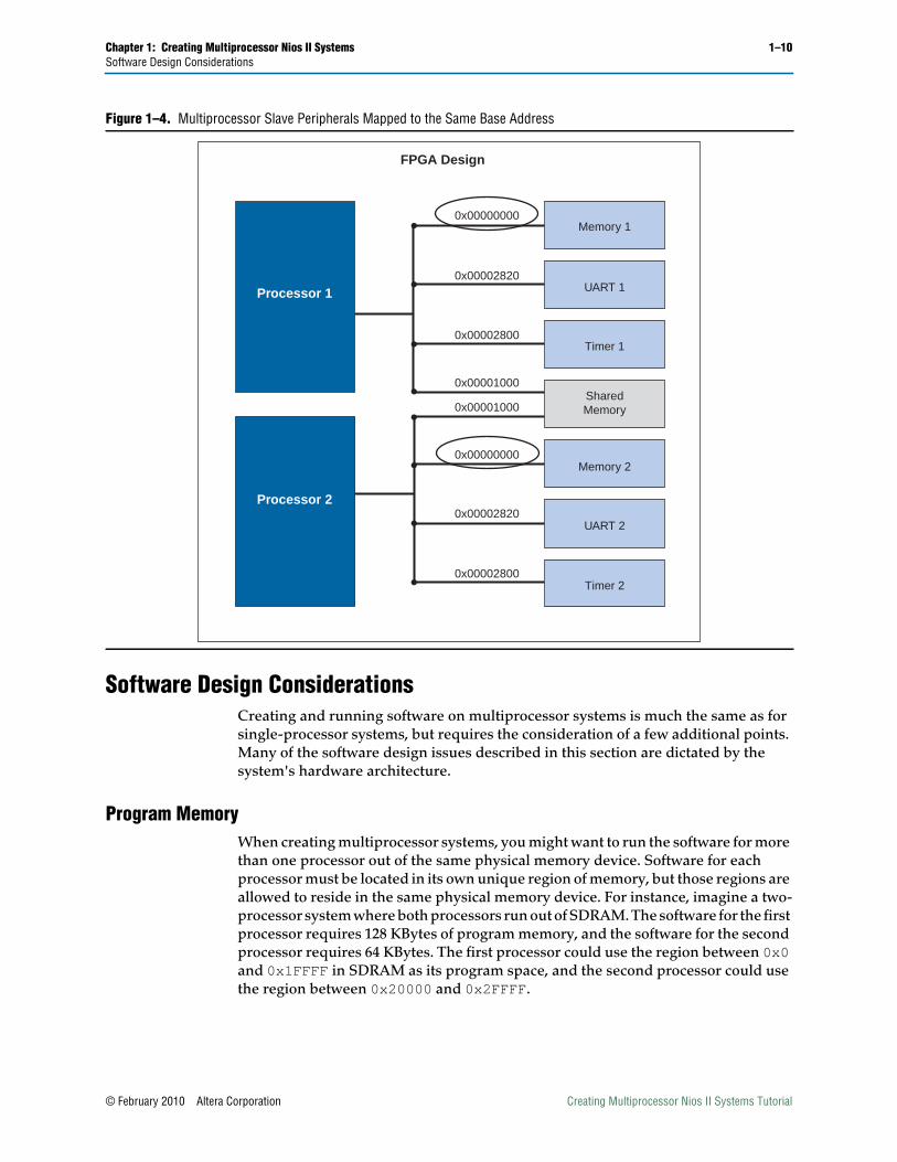
Multiprocessors and Overlapping Address SpaceSingle-processor systems typically prohibit more than one slave peripheral fromoccupying the same address space because this arrangement causes conflicts. Inmultiprocessorsystemshowever,separateslaveperipheralscanoccupythesamebaseaddress and not conflict, as long as each of those peripherals is exclusively masteredbyadifferentprocessor.Becausenoteveryslaveperipheral isnecessarilymasteredbyeveryprocessor,eachprocessormighthaveadifferentviewof thesystem. IfprocessorA is connected to a slave peripheral mapped to address 0x4000, processor B mayconnect to a separate slave peripheral, also mapped to address 0x4000, as long asprocessor A is not connected to processor B's slave peripheral and processor B is notconnected to processor A's slave peripheral. In effect, the point-to-point connectivityallows the two processors to have separate address spaces. Figure 1–4 shows a blockdiagram of a sample multiprocessor system with different slave components mappedto the same base address.
© February 2010 Altera Corporation Creating Multiprocessor Nios II Systems TutorialPreliminary
Chapter 1: Creating Multiprocessor Nios II Systems 1–10Software Design Considerations
Software Design ConsiderationsCreating and running software on multiprocessor systems is much the same as forsingle-processor systems, but requires the consideration of a few additional points.Many of the software design issues described in this section are dictated by thesystem's hardware architecture.
Program MemoryWhen creating multiprocessor systems, you might want to run the software for morethan one processor out of the same physical memory device. Software for eachprocessor must be located in its own unique region of memory, but those regions areallowed to reside in the same physical memory device. For instance, imagine a two-processor system where both processors run out of SDRAM. The software for the firstprocessor requires 128 KBytes of program memory, and the software for the secondprocessor requires 64 KBytes. The first processor could use the region between 0x0and 0x1FFFF in SDRAM as its program space, and the second processor could usethe region between 0x20000 and 0x2FFFF.
Figure 1–4. Multiprocessor Slave Peripherals Mapped to the Same Base Address
FPGA Design
Processor 10x00002820
0x00002800
0x00001000
0x00001000
0x00002820
0x00002800
0x00000000
Memory 1
Processor 2
Timer 2
UART 2
Memory 2
SharedMemory
Timer 1
UART 1
0x00000000
© February 2010 Altera Corporation Creating Multiprocessor Nios II Systems TutorialPreliminary
Chapter 1: Creating Multiprocessor Nios II Systems 1–11Software Design Considerations
The Nios II SBT and SOPC Builder provide a simple scheme of memory partitioningthat allows multiple processors to run their software out of different regions of thesame physical memory. The partitioning scheme uses the exception address for eachprocessor, which is set in SOPC Builder, to determine the region of memory fromwhich each processor will be allowed to run its software. The Nios II SBT is ultimatelyresponsible for the linking of the processors' software and determining where thesoftware will reside in memory; it uses the exception addresses that were set for eachprocessor in SOPC Builder to calculate where the different code sections will belinked. The Nios II SBT provides each processor its own section within memory fromwhich it can run its software. If the software for two different processors is linked tothe same physical memory, then the exception address of each processor is used todetermine the base address of the region which that processor's software can occupy.The end address of the region is determined by the next exception address found inthat physical memory, or the end of that physical memory, whichever comes first.
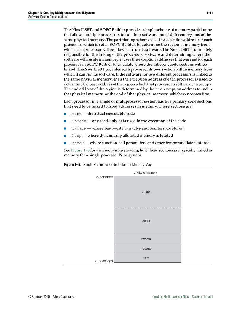
Each processor in a single or multiprocessor system has five primary code sectionsthat need to be linked to fixed addresses in memory. These sections are:
■ .text — the actual executable code
■ .rodata — any read-only data used in the execution of the code
■ .rwdata — where read-write variables and pointers are stored
■ .heap — where dynamically allocated memory is located
■ .stack — where function-call parameters and other temporary data is stored
See Figure 1–5 for a memory map showing how these sections are typically linked inmemory for a single processor Nios system.
Figure 1–5. Single Processor Code Linked in Memory Map
1 Mbyte Memory
0x00FFFFF
0x00000000
.stack
.heap
.rwdata
.rodata
.text
© February 2010 Altera Corporation Creating Multiprocessor Nios II Systems TutorialPreliminary
Chapter 1: Creating Multiprocessor Nios II Systems 1–12Software Design Considerations
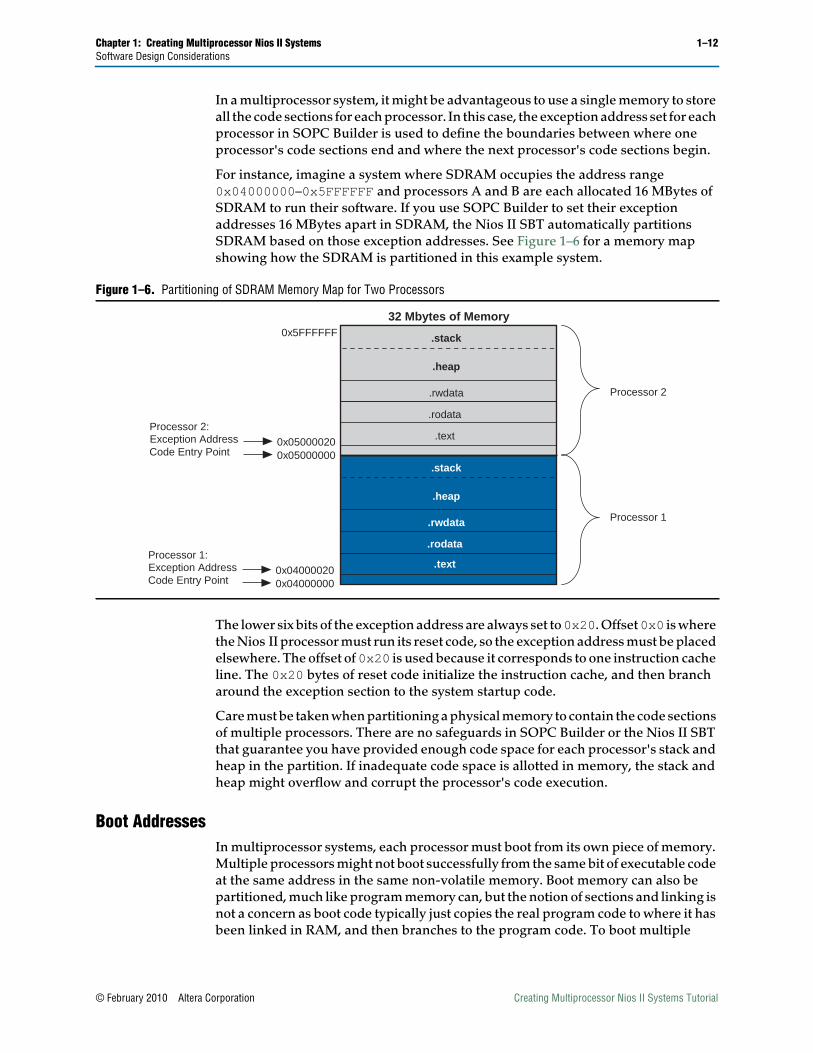
In a multiprocessor system, it might be advantageous to use a single memory to storeall the code sections for each processor. In this case, the exception address set for eachprocessor in SOPC Builder is used to define the boundaries between where oneprocessor's code sections end and where the next processor's code sections begin.
For instance, imagine a system where SDRAM occupies the address range0x04000000–0x5FFFFFF and processors A and B are each allocated 16 MBytes ofSDRAM to run their software. If you use SOPC Builder to set their exceptionaddresses 16 MBytes apart in SDRAM, the Nios II SBT automatically partitionsSDRAM based on those exception addresses. See Figure 1–6 for a memory mapshowing how the SDRAM is partitioned in this example system.
The lower six bits of the exception address are always set to 0x20. Offset 0x0 is wherethe Nios II processor must run its reset code, so the exception address must be placedelsewhere. The offset of 0x20 is used because it corresponds to one instruction cacheline. The 0x20 bytes of reset code initialize the instruction cache, and then brancharound the exception section to the system startup code.
Care must be taken when partitioning a physical memory to contain the code sectionsof multiple processors. There are no safeguards in SOPC Builder or the Nios II SBTthat guarantee you have provided enough code space for each processor's stack andheap in the partition. If inadequate code space is allotted in memory, the stack andheap might overflow and corrupt the processor's code execution.
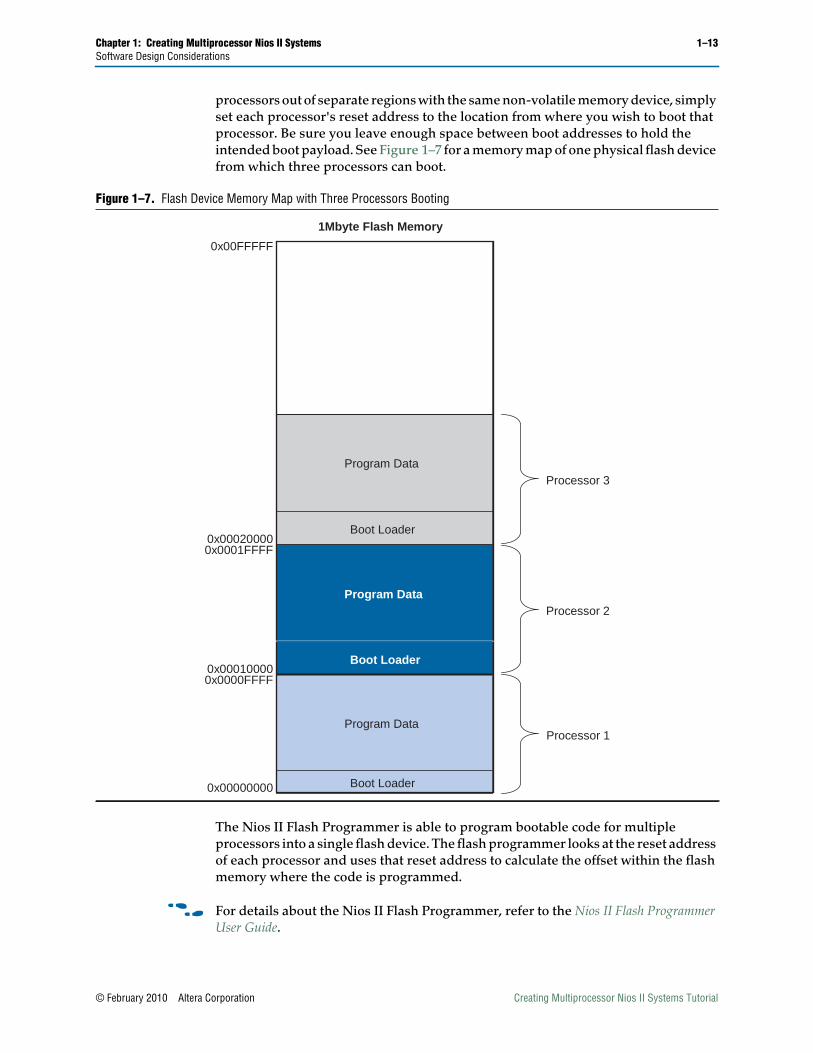
Boot AddressesIn multiprocessor systems, each processor must boot from its own piece of memory.Multiple processors might not boot successfully from the same bit of executable codeat the same address in the same non-volatile memory. Boot memory can also bepartitioned, much like program memory can, but the notion of sections and linking isnot a concern as boot code typically just copies the real program code to where it hasbeen linked in RAM, and then branches to the program code. To boot multiple
Figure 1–6. Partitioning of SDRAM Memory Map for Two Processors
0x5FFFFFF
32 Mbytes of Memory
Processor 1
Processor 2
.text
.rodata
.rwdata
.heap
.stack
.text
.rodata
.rwdata
0x05000020Exception Address
0x05000000Code Entry Point
Processor 2:
Exception Address
0x04000000Code Entry Point
Processor 1:
0x04000020
.heap
.stack
© February 2010 Altera Corporation Creating Multiprocessor Nios II Systems TutorialPreliminary
Chapter 1: Creating Multiprocessor Nios II Systems 1–13Software Design Considerations
processors out of separate regions with the same non-volatile memory device, simplyset each processor's reset address to the location from where you wish to boot thatprocessor. Be sure you leave enough space between boot addresses to hold theintended boot payload. See Figure 1–7 for a memory map of one physical flash devicefrom which three processors can boot.
The Nios II Flash Programmer is able to program bootable code for multipleprocessors into a single flash device. The flash programmer looks at the reset addressof each processor and uses that reset address to calculate the offset within the flashmemory where the code is programmed.
f For details about the Nios II Flash Programmer, refer to the Nios II Flash ProgrammerUser Guide.
Figure 1–7. Flash Device Memory Map with Three Processors Booting
0x00000000
0x00FFFFF
1Mbyte Flash Memory
Boot Loader
Program DataProcessor 1
Processor 2
Processor 3
0x0000FFFF
0x0001FFFF0x00020000
0x00010000
Program Data
Boot Loader
Program Data
Boot Loader
© February 2010 Altera Corporation Creating Multiprocessor Nios II Systems TutorialPreliminary

Chapter 1: Creating Multiprocessor Nios II Systems 1–14Software Design Considerations
c YoumustexercisecautionwhenconnectingmultipleNios IIprocessorstoasingleCFIflash memory device. Because no support mechanism exists in the CFI flash driver toallow a processor to confirm that another processor is not currently accessing the flashmemorydevice,areadoperationcanreturncorrupteddata.Specifically, ifaprocessorattempts to read from a CFI flash memory device currently not in read mode, the readoperation does not access the data on the flash correctly. If another processor issues aquery to the flash memory device immediately prior to the first processor’s readattempt, the flash memory device is in command mode while it processes the query,and the read operation cannot read the data correctly.
An example of a multiprocessor system in which this caution is relevant, is a systemin which multiple processors boot from the same CFI flash memory. In such systems,you must remove CFI flash memory initialization from the alt_main() function runby every Nios II processor. Should you find it necessary for a single processor toinitialize CFI flash memory, you must ensure that it does so only after all the otherprocessors have completed their boot processes. Otherwise, if the processors bootsimultaneously, a race condition occurs when the first processor to jump out of theboot copier and start running the application code runs alt_main() and initializesthe flash memory driver while another processor is still trying to read its own bootcode. During this initialization, the second processor’s read operations of its own bootcopier return corrupted data.
1 Altera recommends that you designate one Nios II processor as the flash master, andallow only the flash master to read from or write to the flash memory device, in anysystem that connects multiple Nios II processors to a single flash memory device. Thedesignated processor can read the application images from the flash memory devicefor the other processors.
If you choose to allow multiple Nios II processors to boot from the same CFI flashmemory device, to ensure safe access to the CFI flash memory, you must remove theCFI flash memory driver initialization from the alt_main() function for all but oneprocessor, and that processor must confirm boot completion by all the otherprocessors before proceeding with the CFI flash memory driver initialization.
f For information about complex boot procedures, refer to AN458: Alternative Nios IIBoot Methods.
Running and Debugging Multiprocessor Systems from the Nios II SBT for EclipseThe Nios II SBT for Eclipse includes a number of features that can help in thedevelopment of software for multiprocessor systems. Most notable is the ability of theNios II SBT for Eclipse to perform simultaneous debug for multiple processors.Multiple debug sessions can run at the same time on a multiprocessor system and canpause and resume each processor independently. Breakpoints can also be setindividually per processor. If one processor hits a breakpoint, it does not halt or affectthe operation of the other processors. Debug sessions can be launched and stoppedindependently.
© February 2010 Altera Corporation Creating Multiprocessor Nios II Systems TutorialPreliminary
Chapter 1: Creating Multiprocessor Nios II Systems 1–15Design Example
Design ExampleThe following exercise shows you how to build a two-processor Nios II system withSOPC Builder, starting with the neek_vic_single_91sp1_v1 example design as atemplate. You create two application projects and two BSP software projects andimport them to the Nios II SBT for Eclipse, one BSP project for each processor. Thesoftware for cpu1 runs a TCP/IP stack and accepts commands for adjusting thefrequency of a blinking LED through a telnet connection. cpu1 uses the hardwaremailbox component to pass LED frequency change messages to cpu2. The softwarefor cpu2 uses the hardware mailbox core to read these messages and adjust the LEDfrequency accordingly. cpu2 continually checks the mailbox for new messages, and ifit finds one, adjusts the LED frequency.
Hardware and Software RequirementsTo use this design example you must have the following:
■ Quartus® II Software version 9.1 SP1 or higher
■ Nios II Embedded Evaluation Kit (NEEK) with the following connections:
■ Connected through a USB-Blaster connection to the host computer
■ Connected through an Ethernet cable to the network
If you do not have a NEEK, you can follow the hardware development steps, but youwill not be able to download the complete system to a working board.
Installation NotesFor installation notes specific to Altera software versions, refer to the readme.txt fileincluded in your Multiprocessor_Tutorial.zip installation.
Creating the Hardware SystemIn the following steps you create a multiprocessor system by starting with theneek_vic_single_91sp1_v1 hardware example design available with this tutorial inMultiprocessor_Tutorial.zip, and adding an additional processor, an additionaltimer, an additional vectored interrupt controller, a hardware mailbox component, ashared on-chip memory, and a hardware mutex component. Your final system shouldbe identical to that in the neek_vic_multi_91sp1_v1 hardware design available withthis tutorial in Multiprocessor_Tutorial.zip, for comparison purposes. If you do nothave a NEEK, you can still follow these steps to learn how to design multiprocessorhardware.
Getting Started with the neek_vic_single_91sp1_v1 Example DesignTo begin building a multiprocessor system sharing resources, perform the followingsteps:
1. Unzip the Multiprocessor_Tutorial.zip file.
2. Copy the neek_vic_single_91sp1_v1 folder to a working directory of your choice.Make sure the path name has no spaces.
3. Open the Quartus II software.
© February 2010 Altera Corporation Creating Multiprocessor Nios II Systems TutorialPreliminary
Chapter 1: Creating Multiprocessor Nios II Systems 1–16Design Example
4. On the File menu, click Open Project (not Open).
5. Browse and load the Quartus II Project File (.qpf) from the newly-createddirectory.
6. On the Tools menu, click SOPC Builder.
7. Click cpu1_vic.
8. Click the blue arrow Move Up button several times to move cpu1_vic directlyunder cpu1.
1 In this tutorial, you must name the hardware components exactly according to theinstructions. If your component names differ from the names printed here, thesoftware example will not work.
Adding a Second ProcessorIn the next series of steps, you add a second Nios II processor to the system. You use aNios II/f processor because it is the fastest choice. If your FPGA is resourceconstrained by your other application needs, you can use the smaller Nios II/sprocessor.
To add a second processor, perform the following steps:
1. In the Component Library on the left side of the System Contents tab, expandProcessors, and select Nios II Processor.
2. Click Add. The Nios II Processor MegaWizard™ interface appears, displaying theCore Nios II page.
3. Specify the settings shown in Table 1–1.
1 Recall from “Program Memory” on page 1–10 that the exception addressesdetermine how code memory is partitioned between processors. In thistutorial, each of the two processors runs its software from 16 Mbyte ofSDRAM, so you set each processor's exception address within SDRAM,separated by 0x1000000 (16 MBytes).
Table 1–1. cpu2 Parameter Settings
Parameter Value
Nios II Core Nios II/f
Hardware Multiply None
Hardware Divide Off
Reset Vector: Memory ddr_sdram
Reset Vector: Offset 0x1000000
Exception Vector: Memory ddr_sdram
Exception Vector: Offset 0x1000020
Include MMU Off
Include MPU Off
© February 2010 Altera Corporation Creating Multiprocessor Nios II Systems TutorialPreliminary
Chapter 1: Creating Multiprocessor Nios II Systems 1–17Design Example
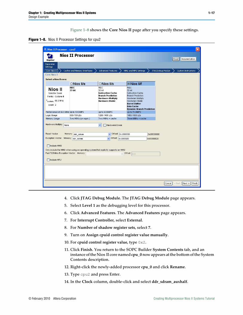
Figure 1–8 shows the Core Nios II page after you specify these settings.
4. Click JTAG Debug Module. The JTAG Debug Module page appears.
5. Select Level 1 as the debugging level for this processor.
6. Click Advanced Features. The Advanced Features page appears.
7. For Interrupt Controller, select External.
8. For Number of shadow register sets, select 7.
9. Turn on Assign cpuid control register value manually.
10. For cpuid control register value, type 0x2.
11. Click Finish. You return to the SOPC Builder System Contents tab, and aninstance of the Nios II core named cpu_0 now appears at the bottom of the SystemContents description.
12. Right-click the newly-added processor cpu_0 and click Rename.
13. Type cpu2 and press Enter.
14. In the Clock column, double-click and select ddr_sdram_auxhalf.
Figure 1–8. Nios II Processor Settings for cpu2
© February 2010 Altera Corporation Creating Multiprocessor Nios II Systems TutorialPreliminary
1–18 Chapter 1: Creating Multiprocessor Nios II SystemsDesign Example
15. In the Base column, double-click and type 0x06020000.
16. Click the blue arrow Move Up button several times to move cpu2 directly undercpu1_timer.
1 Error messages still appear in the SOPC Builder messages window. This is becauseSOPC Builder does not know that you plan to connect this processor with othercomponents in the system. Ignore the error messages for now. You will fix these errorsin later steps.
Adding a Vectored Interrupt Controller for cpu2ProcessorsinanSOPCBuildersystemshouldnotshareavectoredinterruptcontroller(VIC). Not every processor requires aVIC; however, multiple processors cannot sharea VIC. A VIC sends peripheral interrupts to the processor to which it is connected. Toprotect data integrity, each peripheral interrupt must be handled by a singleprocessor.
c SOPC Builder allows you to connect a peripheral to more than one VIC. You mustcheck your system manually to ensure that each peripheral interrupt is routed to nomore than one VIC.
To add a VIC for cpu2, perform the following steps:
1. In the Component Library, expand Processor Additions and then click VectoredInterrupt Controller.
2. Click Add. The VIC MegaWizard interface appears.
3. Specify the following settings:
■ Number of Interrupts: 8
■ Requested Interrupt Level Width: 4
■ DAISY CHAIN ENABLE: Off
4. Click Finish. You return to the SOPC Builder System Contents tab, and aninstance of the VIC named vic_0 now appears at the bottom of the SystemContents description.
5. Right-click vic_0 and click Rename.
6. Type cpu2_vic and press Enter.
7. In the Clock column, double-click and select ddr_sdram_auxhalf.
8. In the Base column, double-click and type 0x06021000.
9. Click the blue arrow Move Up button several times to move cpu2_vic directlyunder cpu2.
10. Using the connection matrix, make the following port connections:
■ cpu2_vic/dummy_master to cpu2_vic/csr_access
■ cpu2/data_master to cpu2_vic/csr_access
■ cpu2_vic/interrupt_controller_out to cpu2/interrupt_controller_in
Creating Multiprocessor Nios II Systems Tutorial © February 2010 Altera CorporationPreliminary
Chapter 1: Creating Multiprocessor Nios II Systems 1–19Design Example
1 If you do not see the connection matrix, on the View menu, click Show ConnectionsColumn.
Adding a Timer for cpu2As mentioned earlier, it is typically not recommended for multipleprocessors to sharenon-memory or non-multiprocessor coordination peripherals, so in this section youadd a separate timer peripheral for the second processor in this system.
To add a timer for cpu2, perform the following steps:
1. In the Component Library, expand Peripherals, expand MicrocontrollerPeripherals, and then click Interval Timer.
2. Click Add. The Interval Timer MegaWizard interface appears.
3. Specify the following settings:
■ Timeout period: 1 ms
■ Timer counter size: 32
■ Under Hardware Options, in the Presets list, select Full-featured.
4. Click Finish. You return to the SOPC Builder System Contents tab, and aninstance of the interval timer named timer_0 now appears at the bottom of theSystem Contents description.
5. Right-click timer_0 and click Rename.
6. Type cpu2_timer and press Enter. This is the timer for cpu2.
7. In the Clock column, double-click and select ddr_sdram_auxhalf.
8. In the Base column, double-click and type 0x06022000.
9. Click the blue arrow Move Up button to move cpu2_timer directly undercpu2_vic.
10. In the connection matrix, connect cpu2_timer/s1 to cpu2/data_master only, anddisconnect cpu2_ timer from all other masters.
11. In the IRQ connection matrix (on the rightmost side of the System Contents tab),type 0 at the cpu2_vic to cpu2_timer connection. This value allows cpu2_timer tointerrupt cpu2 with a priority setting of 0, which is the highest priority. Do notspecify any interrupt priority for the cpu1_vic, because the cpu2_timer shouldonly interrupt the cpu2 processor.
1 If your system contents are displayed using the default filter, the labels yousee when you move the mouse over the potential interrupt connections inthe IRQ column do not make sense. Despite the port names listed, the portsthat are connected in the IRQ column are the irq_input and irq ports of thecomponents. To see the correct labels, in the System Contents tab, click theFilters button and for Filter, select All. To return to the more compressedpresentation, in the System Contents tab, click the Filters button and forFilter, select Default. Whether or not you display the correct labels, thecorrect ports are connected in the IRQ column.
© February 2010 Altera Corporation Creating Multiprocessor Nios II Systems TutorialPreliminary
1–20 Chapter 1: Creating Multiprocessor Nios II SystemsDesign Example
Adding a Message Buffer MemoryIn this section, you add an on-chip memory to the system. The hardware mailboxcomponent uses this memory as a message buffer to pass messages betweenprocessors. This memory must be shared by both processors in the system. Theprocessors use the mailbox core to provide mutually exclusive memory access,protecting the memory's contents from corruption.
To add a message buffer memory, perform the following steps:
1. In the Component Library, expand Memories and Memory Controllers, expandOn-Chip, and then click On-Chip Memory (RAM or ROM).
2. Click Add. The On-Chip Memory (RAM or ROM) MegaWizard interface appears.
3. Under Memory type, select RAM (Writable).
4. For Data width, select 32.
5. In the Total memory size box, type 4096 and select Bytes to specify a memory sizeof 4 KBytes.
6. Under Read latency, for Slave s1, select 1.
7. Click Finish. You return to the SOPC Builder System Contents tab, and aninstance of the on-chip memory named onchip_memory2_0 now appears at thebottom of the System Contents description.
8. Right-click onchip_memory2_0 and click Rename.
9. Type message_buffer_ram and press Enter. This memory is used as a messagebuffer for the two processors in your multiprocessor system to communicatethrough the hardware mailbox component.
10. In the Clock column, double-click and select ddr_sdram_auxhalf.
11. In the Base column, double-click and type 0x07000000.
12. Click the blue arrow Move Up button to move message_buffer_ram directlyunder led_pio.
Connecting Shared Memory and System Output ResourcesNow you need to properly connect all the resources that are shared betweenprocessors inthesystemusingSOPCBuilder'sconnectionmatrixandIRQconnectionmatrix.
Toproperlyconnect thememoryandsystemoutputresources inthesystemsharedbythe multiple processors, perform the following steps:
1. In the connection matrix, ensure that each timer is connected only to the datamaster for its processor, by disconnecting cpu1_timer from cpu2/data_master.
2. In the connection matrix, ensure that the System ID peripheral named sysid isconnected to the data masters for both processors.
3. In the connection matrix, connect message_buffer_ram to the data masters forboth processors.
4. In the connection matrix, ensure that the ddr_half_rate_bridge is connected to theinstructionanddatamastersforeachprocessor,allowingbothprocessorstoaccessddr_sdram.
Creating Multiprocessor Nios II Systems Tutorial © February 2010 Altera CorporationPreliminary

Chapter 1: Creating Multiprocessor Nios II Systems 1–21Design Example
5. In the connection matrix, disconnect cpu2/instruction_master from allcomponents except cpu2/jtag_debug_module, ddr_half_rate_bridge, andflash_tristate_bridge.
6. In the connection matrix, disconnect cpu2/data_master from all componentsexcept cpu2/jtag_debug_module, sysid, cpu2_vic/csr_access, cpu2_timer,led_pio, message_buffer_ram, ddr_half_rate_bridge, and flash_tristate_bridge.
7. In the IRQ connection matrix, ensure that cpu2_vic is connected only to thecpu2_timer. To remove an IRQ connection, erase the default IRQ number. In thisstep, you disconnect all IRQ lines involving the cpu2_vic from all resources, exceptfor the cpu2_vic to cpu2_timer IRQ connection you set in step 11 in “Adding aTimer for cpu2” on page 1–19.
1 Recall that to view the correct port names for the IRQ connections, youmust use the All filter in the System Contents tab.
8. In the IRQ connection matrix, ensure that cpu1_vic is not connected to thecpu2_timer.
9. In the IRQ connection matrix, connect cpu1_vic to all peripherals except thecpu2_timer by setting unique interrupt numbers for each potential cpu1_vic IRQconnection.
10. To design the system so that cpu2 controls the blinking of the LED on the NEEK,perform the following steps:
a. In the connection matrix, disconnect cpu1/data_master from the led_piocomponent.
b. In the connection matrix, connect cpu2/data_master to the led_pio component.
Adding a Hardware Mailbox ComponentBecause your multiprocessor system shares data in memory, it must include an SOPCBuilderhardwarecomponentformultiprocessorcoordinationtoprotect thatmemoryfrom data corruption.
To add a hardware mailbox, perform the following steps:
1. In the Component Library, expand Peripherals, expand MultiprocessorCoordination, and then click Mailbox.
2. Click Add. The Mailbox MegaWizard interface appears.
3. Leave the Memory module blank.
4. For Shared mailbox memory offset, type 0x800.
5. For Mailbox size (bytes), type 0x100.
6. Click Finish. You return to the SOPC Builder System Contents tab, and aninstance of the mailbox named mailbox_0 now appears at the bottom of theSystem Contents description.
7. Right-click mailbox_0 and click Rename.
8. Type message_buffer_mailbox and press Enter.
9. In the Clock column, double-click and select ddr_sdram_auxhalf.
© February 2010 Altera Corporation Creating Multiprocessor Nios II Systems TutorialPreliminary
1–22 Chapter 1: Creating Multiprocessor Nios II SystemsDesign Example
10. In the Base column, double-click and type 0x07009000.
11. Click the blue arrow Move Up button to move message_buffer_mailbox directlyunder message_buffer_ram.
Optionally Adding a Hardware Mutex ComponentThe software examples for this tutorial do not use a separate hardware mutexcomponent. Instead, they coordinate multiprocessor communication through thehardware mailbox component. However, this section provides you with theinstructions to add a mutex to your system, to demonstrate its availability and toillustrate how to connect a hardware mutex component in a multiprocessor SOPCBuilder system.
To add the hardware mutex peripheral, perform the following steps:
1. In the Component Library, expand Peripherals, expand MultiprocessorCoordination, and then click Mutex.
2. Click Add. The Mutex MegaWizard interface appears.
3. Click Finish to accept the default settings for this component. You return to theSOPC Builder System Contents tab, and an instance of the mutex named mutex_0now appears at the bottom of the System Contents description.
4. Right-click mutex_0 and click Rename.
5. Type message_buffer_mutex and press Enter.
6. In the Clock column, double-click and select ddr_sdram_auxhalf.
7. In the Base column, double-click and type 0x07008000.
8. Click the blue arrow Move Up button to move message_buffer_mutex directlyunder led_pio.
Connecting Shared Multiprocessor Coordination ResourcesNow you need to properly connect all the coordination resources that are sharedbetween processors in the system using SOPC Builder's connection matrix and IRQconnection matrix.
To properly connect the shared coordination resources in the multiprocessor system,perform the following steps:
1. In the connection matrix, connect message_buffer_mutex to the data_master portsof both processors.
2. Ensure that message_buffer_mutex is not connected to either processor’sinstruction_master port.
3. In the connections matrix, connect message_buffer_mailbox to the data_masterports of both processors.
4. Ensure that message_buffer_mailbox is not connected to either processor’sinstruction_master port.
5. Double-clickthemessage_buffer_mailboxcomponent.TheMailboxMegaWizardinterface appears.
6. For memory module, select message_buffer_ram.
Creating Multiprocessor Nios II Systems Tutorial © February 2010 Altera CorporationPreliminary

Chapter 1: Creating Multiprocessor Nios II Systems 1–23Design Example
7. Click Finish.
1 None of the I/O components should be connected to multiple processors. Unusedconnections consume Avalon resources and FPGA logic elements, possibly affectingsystem fMAX.
Figure 1–9 shows a system in SOPC Builder after these changes. It shows the newcomponents that implement the message buffer and the required connectivity for thesystem.
The neek_vic_multi_91sp1_v1 example design is also available in theMultiprocessor_Tutorial.zip file. You can compare your completed system to thepredefined system located in the neek_vic_multi_91sp1_v1 subdirectory of theextracted directory.
Generating and Compiling the SystemIn this section, you generate HDL for the system you just constructed in SOPCBuilder, and then compile the project in the Quartus II software to produce aprogramming file.
Figure 1–9. Shared Resource Connections
© February 2010 Altera Corporation Creating Multiprocessor Nios II Systems TutorialPreliminary
1–24 Chapter 1: Creating Multiprocessor Nios II SystemsCreating Software for the Multiprocessor System
To generate and compile the system, perform the following steps:
1. Click the System Generation tab.
2. Turn off Simulation. Create project simulator files. System generation executesmuch faster when simulation is off.
3. Click Generate. This might take a few moments. A Stop button replaces theGenerate button, indicating generation is taking place.
4. When generation is complete, the Generate button replaces the Stop button, and aSUCCESS: SYSTEM GENERATION COMPLETED message displays. Click Exitin SOPC Builder to return to the Quartus II software.
5. On the Quartus II Processing menu, click Start Compilation to compile the projectin the Quartus II software.
6. When compilation completes and displays the Full compilation was successfulmessage box, click OK.
7. Click Programmer on the Tools menu.
8. Turn on the Program/Configure checkbox for the SRAM Object File (.sof) in theQuartus II Programmer.
9. Click Start to download the FPGA configuration data to your target hardware.
Creating Software for the Multiprocessor SystemIn the following steps you build one application and one BSP project for eachprocessor in the system using the Nios II SBT, and then import these application andBSP projects to the Nios II SBT for Eclipse, creating a total of four separate softwareprojectsforthemultiprocessorsystem.YouthendebugthesoftwareprojectsusingtheNios II SBT for Eclipse.
The software you run on this system uses the hardware mailbox to exchangemessages between two Nios II processors.
Building the Application and BSP ProjectsTo build the application and BSP projects for this tutorial, perform the following steps:
1. Start a Nios II Command Shell.
2. Change directories to your working directory for the NEEK multiprocessor designexample.
3. Change directories to software_examples/app/cpu2_led.
4. Build the project to be run on the cpu2 processor by typing the followingcommand:
./create-this-app r5. Change directories to software_examples/app/niosII_multicore_socket_server.
6. Build the project to run on the cpu1 processor by typing the following command:
./create-this-app rBoth application software projects and both BSP projects are created and built.
Creating Multiprocessor Nios II Systems Tutorial © February 2010 Altera CorporationPreliminary
Chapter 1: Creating Multiprocessor Nios II Systems 1–25Creating Software for the Multiprocessor System
1 If you make hardware design changes in SOPC Builder, you can most easilyregenerate the application and BSP projects by performing the following steps:
1. Delete all folders and files except the two create-this-bsp scripts fromsoftware_examples/bsp/ucosii_niosII_multicore and software_examples/bsp/cpu2_ucosii_niosII_multicore.
2. Delete the two files software_examples/app/cpu2_led/Makefile andsoftware_examples/app/niosII_multicore_socket_server/Makefile.
3. Repeat the preceding set of steps to build the application and BSP projects.
Starting the Nios II SBT for EclipseIn this section, you start the Nios II SBT for Eclipse and begin importing softwareprojects for the two Nios II processors in the system. To start the Nios II SBT forEclipse from SOPC Builder, perform the following steps:
1. On the Tools menu in the Quartus II software, click SOPC Builder.
2. In SOPC Builder, click the System Generation tab.
3. Click Nios II Software Build Tools for Eclipse. The Nios II SBT for Eclipse starts.
1 If the Workspace Launcher dialog box appears, click OK to accept thedefault workspace. If the Nios II SBT for Eclipse welcome screen appears,click Workbench to continue.
Importing the Software ProjectsIn this section, you import the following four projects to the Nios II SBT for Eclipse:
■ cpu2_led
■ niosII_multicore_socket_server
■ cpu2_ucosii_niosII_multicore
■ ucosii_niosII_multicore
To import the software projects, perform the following steps:
1. In the Nios II SBT for Eclipse, on the File menu, click Import.
2. Click the plus sign to the left of Nios II Software Build Tools Project. The ImportNios II Software Build Tools Project option appears.
3. Highlight Import Nios II Software Build Tools Project, and click Next. TheImport Software Build Tools Project window opens.
4. For Project location, click the Browse button to navigate to one of the four projectsthat you built by running the create-this-app script. For example, browse tosoftware_examples/app, highlight the cpu2_led folder, and click OK.
5. For Project name, enter your project name, for example cpu2_led, and clickFinish.
1 If a dialog box appears with the message Do you want the Nios II SoftwareBuild Tools for Eclipse to manage your makefile for you?, click Yes.
© February 2010 Altera Corporation Creating Multiprocessor Nios II Systems TutorialPreliminary
1–26 Chapter 1: Creating Multiprocessor Nios II SystemsCreating Software for the Multiprocessor System
6. Repeat steps 1 to 5 to import the remaining three projects.
Building the Software ProjectsIn this section, you build the software projects you just imported so they can be run onthe processors in the system.
To build the software projects, perform the following steps:
1. In the Nios II perspective, right-click the project cpu2_led and click Build Project.
2. Right-click the project niosII_multicore_socket_server and click Build Project.
Creating a Debug Configuration for Each ProcessorIn this section, you create a run/debug configuration for each of the target processors.These configurations enable you to run and debug the two software projects you justbuilt on the processors in the system.
To create a debug configuration for each processor, perform the following steps:
1. In the Nios II perspective, click the cpu2_led project.
2. On the Run menu, click Debug Configurations
3. In the configurations list, right-click Nios II Hardware.
4. Click New. A new debug configuration is created for the project.
5. Click the Target Connection tab.
6. If the Name column is not populated, click Refresh Connections.
7. If the Name column remains unpopulated, perform the following steps:
a. In the Project tab, click Advanced. The Nios II ELF Section Properties dialogbox appears.
b. Under Other, set JTAG Debugging Information File name to<working directory>/neek_vic_multi.jdi.
c. Click Close.
8. Under Processors, ensure that the row with Name value cpu2 is selected.
9. Click Apply.
10. Click Debug. The Nios II SBT for Eclipse downloads and launches the cpu2_ledsoftware project on the cpu2 processor, then pauses cpu2 at a breakpoint set onmain().
11. If the Debug Configurations dialog box does not close automatically, click Closeto return to the Nios II perspective.
12. If you are prompted to enter the Nios II Debug perspective, click Yes.
13. If you are not already in the Nios II Debug perspective, change to the Nios IIDebug perspective by clicking the Debug perspective icon in the top right cornerof your Nios II SBT for Eclipse window.
14. Check that the cpu2 debug session, including the call stack, appears in the Nios IIDebug perspective.
Creating Multiprocessor Nios II Systems Tutorial © February 2010 Altera CorporationPreliminary
Chapter 1: Creating Multiprocessor Nios II Systems 1–27Creating Software for the Multiprocessor System
15. To return to the Nios II perspective, click the Nios II perspective icon in the topright corner of your Nios II SBT for Eclipse window. If the Nios II perspective iconis not visible, click the yellow plus-sign Open Perspective button.
16. Repeat steps 1–13 to create and run a debug configuration for the cpu1 targetprocessor, substituting niosII_multicore_socket_server for cpu2_led and cpu1 forcpu2.
You have created, downloaded, and started a debug configuration for each processorin the system. You can now resume the code execution and debug code on each of theprocessors individually, using the normal flow for running or debugging.
Each processor begins executing code immediately after its code is downloaded to theFPGA; the processors do not start in unison. Although each processor begins runningthe code as soon as it is downloaded, the debug configuration ensures that theprocessor stops at a breakpoint set on main().
Debugging the Software Projects on the BoardAfter you download both debug configurations to the NEEK, you must resume codeexecution on each processor.
To run the design example on the NEEK, after the two debug configurations aredownloaded, perform the following steps:
1. To continue the cpu2 debug run past the initial breakpoint, perform the followingsteps:
a. To observe stepping in the debugger, click the main() call stack entry underthe cpu2 debug session.
b. Click the Step Over icon in the toolbar menu to see cpu2 step through thesoftware code.
c. To let cpu2 run freely, click the green arrow Resume icon in the toolbar menu.
2. To continue the cpu1 debug run past the initial breakpoint, perform the followingsteps:
a. Click the main() call stack entry under the cpu1 debug session.
b. Click the green arrow Resume icon in the toolbar menu. The software runningon the cpu1 processor establishes an Ethernet link and displays an IP addressfor cpu1 in the Nios II Console tab.
3. From the command line, telnet to cpu1 at port 30 using the IP address displayed inthe cpu1 startup messages. For example, if the IP address displayed is137.57.235.39, type the following command:
telnet 137.57.235.39 30 r4. The LED Frequency Changing menu appears.
5. Enter values 0 through 9, and watch the corresponding blink rate change for LED1on the NEEK.
6. To quit the telnet session, type q.
© February 2010 Altera Corporation Creating Multiprocessor Nios II Systems TutorialPreliminary
1–28 Chapter 1: Creating Multiprocessor Nios II SystemsConclusion
ConclusionIn this tutorial, you constructed, built software projects for, and debugged software onyour first Nios II multiprocessor system. You have also learned how to use theMailbox component to share system resources between processors. Feel free toexperiment with the system you have created and find interesting new ways of usingmultiple processors in an Altera FPGA.
Altera recommends saving this system to use as a starting point next time you wish tocreate a multiprocessor system.
Creating Multiprocessor Nios II Systems Tutorial © February 2010 Altera CorporationPreliminary
© February 2010 Altera Corporation
Additional Information
Revision HistoryThe following table shows the revision history for this tutorial.
Referenced DocumentsThis tutorial references the following documents:
■ AN458: Alternative Nios II Boot Methods
■ Mailbox Core chapter in Volume 5: Embedded Peripherals of the Quartus IIHandbook
■ MegaCore IP Library Release Notes and Errata
■ Mutex Core chapter in Volume 5: Embedded Peripherals of the Quartus II Handbook
■ Nios II Embedded Design Suite Release Notes and Errata
■ Nios II Flash Programmer User Guide
■ Nios II Hardware Development Tutorial
■ Nios II Software Developer's Handbook
How to Contact AlteraFor the most up-to-date information about Altera products, refer to the followingtable.
Date and Document Version Changes Made Summary of Changes
February 2010v9.1 SP1
Updated for Nios II Software Build Toolsfor Eclipse.
—
December 2007v1.3
Updated for Quartus II 7.2 release: minortext changes.
—
May 2007v1.2
Updated for Quartus II 7.1 release. —
May 2006v1.1
Updated for Quartus II 6.0 release. —
April 2005v1.0
Initial release. —
Contact (1) ContactMethod Address
Technical support Website www.altera.com/support
Technical training Website www.altera.com/training
Email [email protected]
Creating Multiprocessor Nios II Systems Tutorial

Info–2 Additional InformationTypographic Conventions
Typographic ConventionsThis document uses the typographic conventions shown in the following table.
.
Documentation Website www.altera.com/literature
Non-technical support(General)
Email [email protected]
(Software Licensing) Email [email protected]
Note to table:(1) You can also contact your local Altera sales office or sales representative.
Contact (1) ContactMethod Address
Visual Cue Meaning
Bold Type with Initial CapitalLetters
Command names, dialog box titles, checkbox options, and dialog box options areshown in bold, initial capital letters. Example: Save As dialog box.
bold type External timing parameters, directory names, project names, disk drive names, filenames, file name extensions, and software utility names are shown in bold type.Examples: \qdesigns directory, d: drive, chiptrip.gdf file.
ItalicTypewithInitialCapitalLetters Document titles are shown in italic type with initial capital letters. Example: AN 75:High-Speed Board Design.
Italic type Internal timing parameters and variables are shown in italic type.Examples: tPIA, n + 1.
Variable names are enclosed in angle brackets (< >) and shown in italic type.Example: <file name>, <project name>.pof file.
Initial Capital Letters Keyboard keys and menu names are shown with initial capital letters. Examples:Delete key, the Options menu.
“Subheading Title” References to sections within a document and titles of on-line help topics are shownin quotation marks. Example: “Typographic Conventions.”
Courier type Signal and port names are shown in lowercase Courier type. Examples: data1, tdi,input. Active-low signals are denoted by suffix n, e.g., resetn.
Anything that must be typed exactly as it appears is shown in Courier type. Forexample: c:\qdesigns\tutorial\chiptrip.gdf. Also, sections of an actualfile, such as a Report File, references to parts of files (e.g., the AHDL keywordSUBDESIGN), as well as logic function names (e.g., TRI) are shown in Courier.
1., 2., 3., anda., b., c., etc.
Numbered steps are used in a list of items when the sequence of the items isimportant, such as the steps listed in a procedure.
■ ■ Bullets are used in a list of items when the sequence of the items is not important.
v The checkmark indicates a procedure that consists of one step only.
1 The hand points to information that requires special attention.
c A caution calls attention to a condition or possible situation that can damage ordestroy the product or the user’s work.
w A warning calls attention to a condition or possible situation that can cause injury tothe user.
Creating Multiprocessor Nios II Systems Tutorial © February 2010 Altera Corporation

Info–3Typographic Conventions
r The angled arrow indicates you should press the Enter key.
f The feet direct you to more information about a particular topic.
Visual Cue Meaning
© February 2010 Altera Corporation Creating Multiprocessor Nios II Systems Tutorial

Info–4 Additional InformationTypographic Conventions
Creating Multiprocessor Nios II Systems Tutorial © February 2010 Altera Corporation