Embed Size (px)
Citation preview
EECC550 - ShaabanEECC550 - Shaaban#1 Final Review Winter 2000 2-19-2001
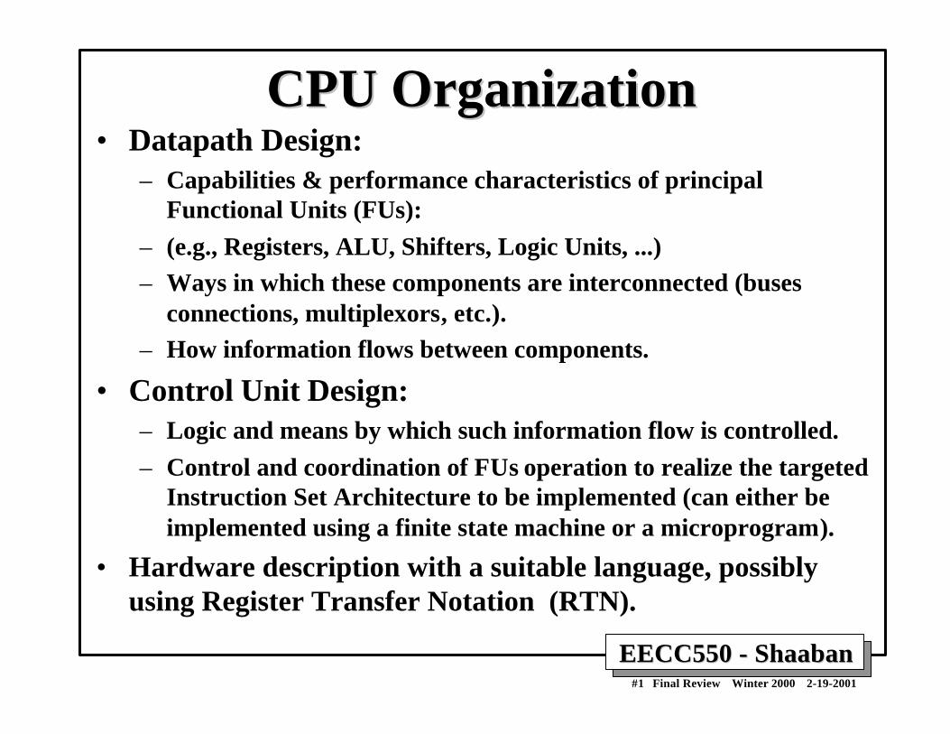
CPU OrganizationCPU Organization• Datapath Design:
– Capabilities & performance characteristics of principalFunctional Units (FUs):
– (e.g., Registers, ALU, Shifters, Logic Units, ...)
– Ways in which these components are interconnected (busesconnections, multiplexors, etc.).
– How information flows between components.
• Control Unit Design:– Logic and means by which such information flow is controlled.
– Control and coordination of FUs operation to realize the targetedInstruction Set Architecture to be implemented (can either beimplemented using a finite state machine or a microprogram).
• Hardware description with a suitable language, possiblyusing Register Transfer Notation (RTN).

EECC550 - ShaabanEECC550 - Shaaban#2 Final Review Winter 2000 2-19-2001
Hierarchy of Computer ArchitectureHierarchy of Computer Architecture
I/O systemInstr. Set Proc.
Compiler
OperatingSystem
Application
Digital DesignCircuit Design
Instruction Set Architecture
Firmware
Datapath & Control
Layout
Software
Hardware
Software/Hardware Boundary
High-Level Language Programs
Assembly LanguagePrograms
Microprogram
Register TransferNotation (RTN)
Logic Diagrams
Circuit Diagrams
Machine Language Program

EECC550 - ShaabanEECC550 - Shaaban#3 Final Review Winter 2000 2-19-2001
• For a specific program compiled to run on a specific machine“A”, the following parameters are provided:
– The total instruction count of the program.– The average number of cycles per instruction (average CPI).– Clock cycle of machine “A”
• How can one measure the performance of this machine running thisprogram?
– Intuitively the machine is said to be faster or has betterperformance running this program if the total execution time isshorter.
– Thus the inverse of the total measured program execution time isa possible performance measure or metric:
PerformanceA = 1 / Execution TimeA
How to compare performance of different machines?
What factors affect performance? How to improve performance?
Computer Performance Measures:Computer Performance Measures:Program Execution TimeProgram Execution Time

EECC550 - ShaabanEECC550 - Shaaban#4 Final Review Winter 2000 2-19-2001
CPU Execution Time: The CPU EquationCPU Execution Time: The CPU Equation• A program is comprised of a number of instructions
– Measured in: instructions/program
• The average instruction takes a number of cycles perinstruction (CPI) to be completed.– Measured in: cycles/instruction
• CPU has a fixed clock cycle time = 1/clock rate– Measured in: seconds/cycle
• CPU execution time is the product of the above threeparameters as follows:
CPU time = Seconds = Instructions x Cycles x Seconds
Program Program Instruction Cycle
CPU time = Seconds = Instructions x Cycles x Seconds
Program Program Instruction Cycle
EECC550 - ShaabanEECC550 - Shaaban#5 Final Review Winter 2000 2-19-2001
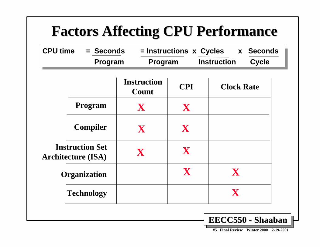
Factors Affecting CPU PerformanceFactors Affecting CPU PerformanceCPU time = Seconds = Instructions x Cycles x Seconds
Program Program Instruction Cycle
CPU time = Seconds = Instructions x Cycles x Seconds Program Program Instruction Cycle
CPI Clock RateInstruction Count
Program
Compiler
Organization
Technology
Instruction SetArchitecture (ISA)
X
X
X
X
X
X
X X
X

EECC550 - ShaabanEECC550 - Shaaban#6 Final Review Winter 2000 2-19-2001
Aspects of CPU Execution TimeAspects of CPU Execution TimeCPU Time = Instruction count x CPI x Clock cycle
Instruction CountInstruction Count
ClockClockCycleCycle
CPICPIDepends on:
CPU OrganizationTechnology
Depends on:
Program Used
CompilerISACPU Organization
Depends on:
Program UsedCompilerISA

EECC550 - ShaabanEECC550 - Shaaban#7 Final Review Winter 2000 2-19-2001
Instruction Types & CPI: An ExampleInstruction Types & CPI: An Example• An instruction set has three instruction classes:
• Two code sequences have the following instruction counts:
• CPU cycles for sequence 1 = 2 x 1 + 1 x 2 + 2 x 3 = 10 cycles
CPI for sequence 1 = clock cycles / instruction count
= 10 /5 = 2
• CPU cycles for sequence 2 = 4 x 1 + 1 x 2 + 1 x 3 = 9 cycles
CPI for sequence 2 = 9 / 6 = 1.5
Instruction class CPI A 1 B 2 C 3
Instruction counts for instruction classCode Sequence A B C 1 2 1 2 2 4 1 1

EECC550 - ShaabanEECC550 - Shaaban#8 Final Review Winter 2000 2-19-2001
Instruction Frequency & CPIInstruction Frequency & CPI• Given a program with n types or classes of
instructions with the following characteristics:
Ci = Count of instructions of typei
CPIi = Average cycles per instruction of typei
Fi = Frequency of instruction typei
= Ci/ total instruction count
Then:
( )∑=
×=n
iii FCPICPI
1

EECC550 - ShaabanEECC550 - Shaaban#9 Final Review Winter 2000 2-19-2001
Instruction Type Frequency & CPI:Instruction Type Frequency & CPI:A RISC ExampleA RISC Example
Typical Mix
Base Machine (Reg / Reg)Op Freq Cycles CPI(i) % TimeALU 50% 1 .5 23%Load 20% 5 1.0 45%Store 10% 3 .3 14%Branch 20% 2 .4 18%
CPI = .5 x 1 + .2 x 5 + .1 x 3 + .2 x 2 = 2.2
( )∑=
×=n
iii FCPICPI
1

EECC550 - ShaabanEECC550 - Shaaban#10 Final Review Winter 2000 2-19-2001
Metrics of Computer PerformanceMetrics of Computer Performance
Compiler
Programming Language
Application
DatapathControl
Transistors Wires Pins
ISA
Function UnitsCycles per second (clock rate).
Megabytes per second.
Execution time: Target workload,SPEC95, etc.
Each metric has a purpose, and each can be misused.
(millions) of Instructions per second – MIPS(millions) of (F.P.) operations per second – MFLOP/s

EECC550 - ShaabanEECC550 - Shaaban#11 Final Review Winter 2000 2-19-2001
Performance Enhancement Calculations:Performance Enhancement Calculations: Amdahl's Law Amdahl's Law
• The performance enhancement possible due to a given designimprovement is limited by the amount that the improved feature is used
• Amdahl’s Law:
Performance improvement or speedup due to enhancement E:
Execution Time without E Performance with E Speedup(E) = -------------------------------------- = --------------------------------- Execution Time with E Performance without E
– Suppose that enhancement E accelerates a fraction F of theexecution time by a factor S and the remainder of the time isunaffected then:
Execution Time with E = ((1-F) + F/S) X Execution Time without EHence speedup is given by:
Execution Time without E 1Speedup(E) = --------------------------------------------------------- = -------------------- ((1 - F) + F/S) X Execution Time without E (1 - F) + F/S
Note: All fractions here refer to original execution time.

EECC550 - ShaabanEECC550 - Shaaban#12 Final Review Winter 2000 2-19-2001
Pictorial Depiction of Amdahl’s LawPictorial Depiction of Amdahl’s Law
Before: Execution Time without enhancement E:
Unaffected, fraction: (1- F)
After: Execution Time with enhancement E:
Enhancement E accelerates fraction F of execution time by a factor of S
Affected fraction: F
Unaffected, fraction: (1- F) F/S
Unchanged
Execution Time without enhancement E 1Speedup(E) = ------------------------------------------------------ = ------------------ Execution Time with enhancement E (1 - F) + F/S

EECC550 - ShaabanEECC550 - Shaaban#13 Final Review Winter 2000 2-19-2001
Amdahl's Law With Multiple Enhancements:Amdahl's Law With Multiple Enhancements:ExampleExample
• Three CPU performance enhancements are proposed with the followingspeedups and percentage of the code execution time affected:
Speedup1 = S1 = 10 Percentage1 = F1 = 20%
Speedup2 = S2 = 15 Percentage1 = F2 = 15%
Speedup3 = S3 = 30 Percentage1 = F3 = 10%
• While all three enhancements are in place in the new design, eachenhancement affects a different portion of the code and only oneenhancement can be used at a time.
• What is the resulting overall speedup?
• Speedup = 1 / [(1 - .2 - .15 - .1) + .2/10 + .15/15 + .1/30)] = 1 / [ .55 + .0333 ] = 1 / .5833 = 1.71
∑ ∑+−=
i ii
ii S
FFSpeedup
)( )1
1
(

EECC550 - ShaabanEECC550 - Shaaban#14 Final Review Winter 2000 2-19-2001
MIPS Instruction FormatsMIPS Instruction Formats
• op: Opcode, operation of the instruction.
• rs, rt, rd: The source and destination register specifiers.
• shamt: Shift amount.
• funct: selects the variant of the operation in the “op” field.
• address / immediate: Address offset or immediate value.
• target address: Target address of the jump instruction.
op target address
02631
6 bits 26 bits
op rs rt rd shamt funct
061116212631
6 bits 6 bits5 bits5 bits5 bits5 bits
op rs rt immediate
016212631
6 bits 16 bits5 bits5 bits
R-Type
I-Type: ALULoad/Store, Branch
J-Type: Jumps

EECC550 - ShaabanEECC550 - Shaaban#15 Final Review Winter 2000 2-19-2001
A Single Cycle MIPS A Single Cycle MIPS Datapath Datapathim
m16
32
ALUctr
Clk
busW
RegWr
3232
busA
32busB
55 5
Rw Ra Rb32 32-bitRegisters
Rs
Rt
Rt
RdRegDst
Exten
der
Mu
x
3216imm16
ALUSrcExtOp
Mu
x
MemtoReg
Clk
Data InWrEn32 Adr
DataMemory
MemWrA
LU
Equal
Instruction<31:0>
0
1
0
1
01
<21:25>
<16:20>
<11:15>
<0:15>
Imm16RdRtRs
=
Ad
der
Ad
der
PC
Clk
00
Mu
x
4
nPC_sel
PC
Ext
Adr
InstMemory

EECC550 - ShaabanEECC550 - Shaaban#16 Final Review Winter 2000 2-19-2001
RegDst ALUctrALUSrc MemtoReg Equal
Instruction<31:0>
<21:25>
<16:20>
<11:15>
<0:15>
Imm16RdRsRt
Adr
InstructionMemory
DATA PATHDATA PATH
ExtOp MemWr
Control UnitControl Unit
Op
<21:25>
Fun
nPC_sel RegWr
<0:25>
Jump_target
Jump
EECC550 - ShaabanEECC550 - Shaaban#17 Final Review Winter 2000 2-19-2001
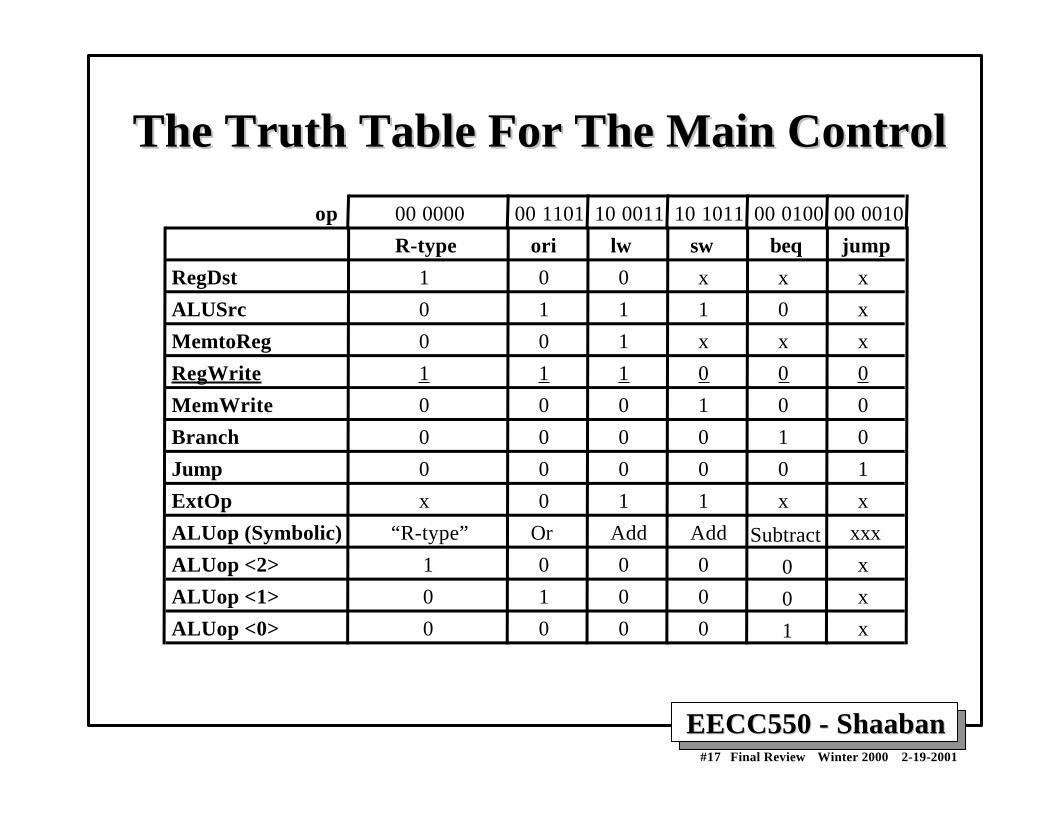
The Truth Table For The Main ControlThe Truth Table For The Main Control
R-type ori lw sw beq jump
RegDst
ALUSrc
MemtoReg
RegWrite
MemWrite
Branch
Jump
ExtOp
ALUop (Symbolic)
1
0
0
1
0
0
0
x
“R-type”
0
1
0
1
0
0
0
0
Or
0
1
1
1
0
0
0
1
Add
x
1
x
0
1
0
0
1
Add
x
0
x
0
0
1
0
x
Subtract
x
x
x
0
0
0
1
x
xxx
op 00 0000 00 1101 10 0011 10 1011 00 0100 00 0010
ALUop <2> 1 0 0 0 0 x
ALUop <1> 0 1 0 0 0 x
ALUop <0> 0 0 0 0 1 x

EECC550 - ShaabanEECC550 - Shaaban#18 Final Review Winter 2000 2-19-2001
Clk
PC
Rs, Rt, Rd,Op, Func
Clk-to-Q
ALUctr
Instruction Memoey Access Time
Old Value New Value
RegWr Old Value New Value
Delay through Control Logic
busARegister File Access Time
Old Value New Value
busB
ALU Delay
Old Value New Value
Old Value New Value
New ValueOld Value
ExtOp Old Value New Value
ALUSrc Old Value New Value
MemtoReg Old Value New Value
Address Old Value New Value
busW Old Value New
Delay through Extender & Mux
RegisterWrite Occurs
Data Memory Access Time
Worst Case Timing (Load)Worst Case Timing (Load)

EECC550 - ShaabanEECC550 - Shaaban#19 Final Review Winter 2000 2-19-2001
MIPS Single Cycle InstructionMIPS Single Cycle InstructionTiming ComparisonTiming Comparison
PC Inst Memory mux ALU Data Mem mux
PC Reg FileInst Memory mux ALU mux
PC Inst Memory mux ALU Data Mem
PC Inst Memory cmp mux
Reg File
Reg File
Reg File
Arithmetic & Logical
Load
Store
Branch
Critical Path
setup
setup

EECC550 - ShaabanEECC550 - Shaaban#20 Final Review Winter 2000 2-19-2001
CPU Design StepsCPU Design Steps1. Analyze instruction set operations using independent
RTN => datapath requirements.
2. Select set of datapath components & establish clockmethodology.
3. Assemble datapath meeting the requirements.
4. Analyze implementation of each instruction to determinesetting of control points that effects the register transfer.
5. Assemble the control logic.
EECC550 - ShaabanEECC550 - Shaaban#21 Final Review Winter 2000 2-19-2001
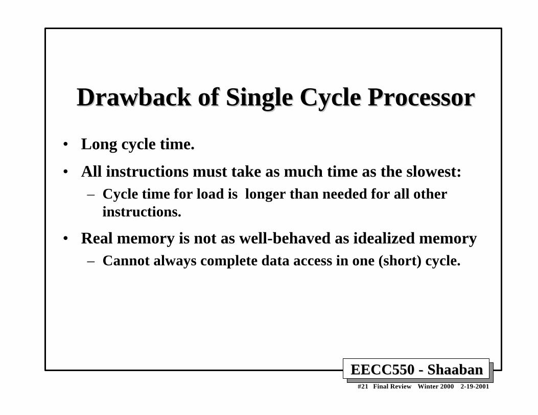
Drawback of Single Cycle ProcessorDrawback of Single Cycle Processor
• Long cycle time.
• All instructions must take as much time as the slowest:– Cycle time for load is longer than needed for all other
instructions.
• Real memory is not as well-behaved as idealized memory– Cannot always complete data access in one (short) cycle.

EECC550 - ShaabanEECC550 - Shaaban#22 Final Review Winter 2000 2-19-2001
Reducing Cycle Time: Multi-Cycle DesignReducing Cycle Time: Multi-Cycle Design• Cut combinational dependency graph by inserting registers / latches.
• The same work is done in two or more fast cycles, rather than one slowcycle.
storage element
Acyclic CombinationalLogic
storage element
storage element
Acyclic CombinationalLogic (A)
storage element
storage element
Acyclic CombinationalLogic (B)
=>

EECC550 - ShaabanEECC550 - Shaaban#23 Final Review Winter 2000 2-19-2001
Instruction Processing CyclesInstruction Processing Cycles
Obtain instruction from program storage
Determine instruction type
Obtain operands from registers
Compute result value or status
Store result in register/memory if needed
(usually called Write Back).
Update program counter to address
of next instruction} Common
steps for all instructions
Instruction
Fetch
Instruction
Decode
Execute
Result
Store
Next
Instruction

EECC550 - ShaabanEECC550 - Shaaban#24 Final Review Winter 2000 2-19-2001
Partitioning The Single Cycle DatapathPartitioning The Single Cycle DatapathAdd registers between smallest steps
PC
Nex
t P
C
Ope
rand
Fet
ch Exec Re
g.
File
Mem
Acc
ess
Dat
aM
em
Inst
ruct
ion
Fet
ch
Res
ult S
tore
AL
Uct
r
Reg
Dst
AL
USr
c
Ext
Op
Mem
Wr
nPC
_sel
Reg
Wr
Mem
Wr
Mem
Rd

EECC550 - ShaabanEECC550 - Shaaban#25 Final Review Winter 2000 2-19-2001
Example Multi-cycle DatapathExample Multi-cycle Datapath
PC
Nex
t P
C
Ope
rand
Fet
ch
Ext
ALU Re
g.
File
Mem
Acc
ess
Dat
aM
em
Inst
ruct
ion
Fet
ch
Res
ult S
tore
AL
Uct
r
Reg
Dst
AL
USr
c
Ext
Op
nPC
_sel
Reg
Wr
Mem
Wr
Mem
Rd
IR
A
B
R
M
RegFile
Mem
ToR
eg
Equ
al
Registers added:
IR: Instruction registerA, B: Two registers to hold operands read from register file.R: or ALUOut, holds the output of the ALUM: or Memory data register (MDR) to hold data read from data memory

EECC550 - ShaabanEECC550 - Shaaban#26 Final Review Winter 2000 2-19-2001
Operations In Each CycleOperations In Each Cycle
Instruction Fetch
Instruction Decode
Execution
Memory
WriteBack
R-Type
IR ← ← Mem[PC]
A ←← R[rs]
B ← ← R[rt]
R ←← A + B
R[rd] ← ← R
PC ← ← PC + 4
Logic Immediate
IR ←← Mem[PC]
A ←← R[rs]
R ← ← A OR ZeroExt[imm16]
R[rt] ← ← R PC ← ← PC + 4
Load
IR ←← Mem[PC]
A ←← R[rs]
R ← ← A + SignEx(Im16)
M ← ← Mem[R]
R[rd] ← ← MPC ← ← PC + 4
Store
IR ← ← Mem[PC]
A ←← R[rs]
B ← ← R[rt]
R ←← A + SignEx(Im16)
Mem[R] ←← B
PC ← ← PC + 4
Branch
IR ←← Mem[PC]
A ←← R[rs]
B ← ← R[rt]
If Equal = 1
PC ←← PC + 4 +
(SignExt(imm16) x4)
else
PC ←← PC + 4

EECC550 - ShaabanEECC550 - Shaaban#27 Final Review Winter 2000 2-19-2001
Finite State Machine (FSM) Control ModelFinite State Machine (FSM) Control Model
• State specifies control points for Register Transfer.
• Transfer occurs upon exiting state (same falling edge).
State X
Register TransferControl Points
Depends on Input
Control State
Next StateLogic
Output Logic
inputs (conditions)
outputs (control points)

EECC550 - ShaabanEECC550 - Shaaban#28 Final Review Winter 2000 2-19-2001
Control Specification For Multi-cycle CPUControl Specification For Multi-cycle CPUFinite State Machine (FSM)Finite State Machine (FSM)
IR ←← MEM[PC]
R-type
A ←← R[rs]B ←← R[rt]
R ← ← A fun B
R[rd] ← ← RPC ←← PC + 4
R ← ← A or ZX
R[rt] ←← RPC ← ← PC + 4
ORi
R ← ← A + SX
R[rt] ←← MPC ←← PC + 4
M ← ← MEM[R]
LW
R ← ← A + SX
MEM[R] ←← BPC ← ← PC + 4
BEQ & Equal
BEQ & ~Equal
PC ←← PC + 4 PC ← ← PC + SX || 00
SW
“instruction fetch”
“decode / operand fetch”
Exe
cute
Mem
ory
Wri
te-b
ack
To instruction fetch
To instruction fetchTo instruction fetch

EECC550 - ShaabanEECC550 - Shaaban#29 Final Review Winter 2000 2-19-2001
Traditional FSM ControllerTraditional FSM Controller
datapath + state diagram => controldatapath + state diagram => control
• Translate RTN statements intocontrol points.
• Assign states.
• Implement the controller.
EECC550 - ShaabanEECC550 - Shaaban#30 Final Review Winter 2000 2-19-2001
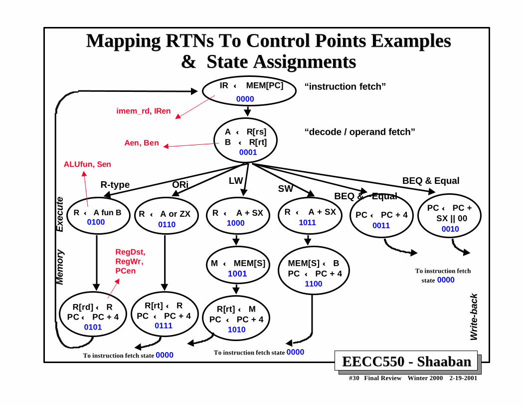
Mapping Mapping RTNsRTNs To Control Points Examples To Control Points Examples& State Assignments& State Assignments
IR ← ← MEM[PC]
0000
R-type
A ←← R[rs]B ←← R[rt] 0001
R ← ← A fun B 0100
R[rd] ← ← RPC ←← PC + 4
0101
R ← ← A or ZX 0110
R[rt] ←← RPC ← ← PC + 4
0111
ORi
R ← ← A + SX 1000
R[rt] ←← MPC ←← PC + 4
1010
M ← ← MEM[S] 1001
LW
R ← ← A + SX 1011
MEM[S] ←← BPC ← ← PC + 4 1100
BEQ & Equal
BEQ & ~Equal
PC ←← PC + 4 0011
PC ← ← PC + SX || 00 0010
SW
“instruction fetch”
“decode / operand fetch”
Exe
cute
Mem
ory
Wri
te-b
ack
imem_rd, IRen
Aen, Ben
ALUfun, Sen
RegDst,RegWr,PCen To instruction fetch
state 0000
To instruction fetch state 0000To instruction fetch state 0000

EECC550 - ShaabanEECC550 - Shaaban#31 Final Review Winter 2000 2-19-2001
Detailed Control SpecificationState Op field Eq Next IR PC Ops Exec Mem Write-Back
en sel A B Ex Sr ALU S R W M M-R Wr Dst0000 ?????? ? 0001 10001 BEQ 0 0011 1 10001 BEQ 1 0010 1 10001 R-type x 0100 1 10001 orI x 0110 1 10001 LW x 1000 1 10001 SW x 1011 1 10010 xxxxxx x 0000 1 10011 xxxxxx x 0000 1 00100 xxxxxx x 0101 0 1 fun 10101 xxxxxx x 0000 1 0 0 1 10110 xxxxxx x 0111 0 0 or 10111 xxxxxx x 0000 1 0 0 1 01000 xxxxxx x 1001 1 0 add 11001 xxxxxx x 1010 1 0 01010 xxxxxx x 0000 1 0 1 1 01011 xxxxxx x 1100 1 0 add 11100 xxxxxx x 0000 1 0 0 1
R

EECC550 - ShaabanEECC550 - Shaaban#32 Final Review Winter 2000 2-19-2001
Alternative Multiple Cycle Datapath (In Textbook)
•Shared instruction/data memory unit• A single ALU shared among instructions• Shared units require additional or widened multiplexors• Temporary registers to hold data between clock cycles of the instruction:
• Additional registers: Instruction Register (IR), Memory Data Register (MDR), A, B, ALUOut
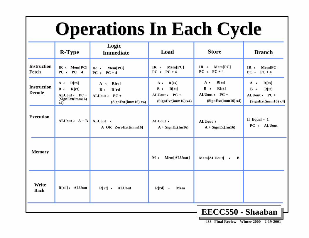
EECC550 - ShaabanEECC550 - Shaaban#33 Final Review Winter 2000 2-19-2001
Operations In Each CycleOperations In Each Cycle
Instruction Fetch
Instruction Decode
Execution
Memory
WriteBack
R-Type
IR ← ← Mem[PC]PC ←← PC + 4
A ←← R[rs]
B ← ← R[rt]
ALUout ←← PC +(SignExt(imm16)x4)
ALUout ←← A + B
R[rd] ← ← ALUout
Logic Immediate
IR ←← Mem[PC]PC ←← PC + 4
A ←← R[rs]
B ← ← R[rt]
ALUout ←← PC +
(SignExt(imm16) x4)
ALUout ← ←
A OR ZeroExt[imm16]
R[rt] ← ← ALUout
Load
IR ←← Mem[PC]PC ←← PC + 4
A ←← R[rs]
B ← ← R[rt]
ALUout ←← PC +
(SignExt(imm16) x4)
ALUout ← ←
A + SignEx(Im16)
M ← ← Mem[ALUout]
R[rd] ← ← Mem
Store
IR ← ← Mem[PC]PC ←← PC + 4
A ←← R[rs]
B ← ← R[rt]
ALUout ←← PC +
(SignExt(imm16) x4)
ALUout ←←
A + SignEx(Im16)
Mem[ALUout] ←← B
Branch
IR ←← Mem[PC]PC ←← PC + 4
A ←← R[rs]
B ← ← R[rt]
ALUout ←← PC +
(SignExt(imm16) x4)
If Equal = 1
PC ← ← ALUout

EECC550 - ShaabanEECC550 - Shaaban#34 Final Review Winter 2000 2-19-2001
Finite State Machine (FSM) Specification Finite State Machine (FSM) SpecificationIR ← MEM[PC]PC ← PC + 4
R-type
ALUout ← A fun B
R[rd] ← ALUout
ALUout ← A op ZX
R[rt] ← ALUout
ORiALUout
← A + SX
R[rt] ← M
M ← MEM[ALUout]
LW
ALUout ← A + SX
MEM[ALUout] ← B
SW
“instruction fetch”
“decode”
Exe
cute
Mem
ory
Writ
e-ba
ck
0000
0001
0100
0101
0110
0111
1000
1001
1010
1011
1100
BEQ
0010
If A = B thenPC ← ALUout
A ← R[rs]B ← R[rt]
ALUout ← ← PC +SX
To instruction fetch
To instruction fetchTo instruction fetch

EECC550 - ShaabanEECC550 - Shaaban#35 Final Review Winter 2000 2-19-2001
MIPS Multi-cycle DatapathMIPS Multi-cycle DatapathPerformance EvaluationPerformance Evaluation
• What is the average CPI?– State diagram gives CPI for each instruction type
– Workload below gives frequency of each type
Type CPIi for type Frequency CPIi x freqIi
Arith/Logic 4 40% 1.6
Load 5 30% 1.5
Store 4 10% 0.4
branch 3 20% 0.6
Average CPI: 4.1
Better than CPI = 5 if all instructions took the same number of clock cycles (5).

EECC550 - ShaabanEECC550 - Shaaban#36 Final Review Winter 2000 2-19-2001
• Control may be designed using one of several initial representations. Thechoice of sequence control, and how logic is represented, can then bedetermined independently; the control can then be implemented with oneof several methods using a structured logic technique.
Initial Representation Finite State Diagram Microprogram
Sequencing Control Explicit Next State Microprogram counter Function + Dispatch ROMs
Logic Representation Logic Equations Truth Tables
Implementation PLA ROMTechnique “hardwired control” “microprogrammed control”
Control Implementation AlternativesControl Implementation Alternatives

EECC550 - ShaabanEECC550 - Shaaban#37 Final Review Winter 2000 2-19-2001
MicroprogrammedMicroprogrammed Control Control• Finite state machine control for a full set of instructions is very
complex, and may involve a very large number of states:– Slight microoperation changes require new FSM controller.
• Microprogramming: Designing the control as a program thatimplements the machine instructions.
• A microprogam for a given machine instruction is a symbolicrepresentation of the control involved in executing the instructionand is comprised of a sequence of microinstructions.
•
• Each microinstruction defines the set of datapath control signalsthat must asserted (active) in a given state or cycle.
• The format of the microinstructions is defined by a number offields each responsible for asserting a set of control signals.
• Microarchitecture:– Logical structure and functional capabilities of the hardware as
seen by the microprogrammer.

EECC550 - ShaabanEECC550 - Shaaban#38 Final Review Winter 2000 2-19-2001
Types of “branching”• Set state to 0 (fetch)• Dispatch i (state 1)• Use incremented address (seq) state number 2
Opcode
State Reg
Microinstruction Address
Inputs
Outputs Control Signal Fields
Microprogram Storage
ROM/PLA
MulticycleDatapath
1
Address Select Logic
Adder
MicroprogramCounter, MicroPC
SequencingControlField
Microprogrammed Microprogrammed Control UnitControl Unit

EECC550 - ShaabanEECC550 - Shaaban#39 Final Review Winter 2000 2-19-2001
List of control Signals Grouped Into FieldsList of control Signals Grouped Into FieldsSignal name Effect when deasserted Effect when asserted
ALUSelA 1st ALU operand = PC 1st ALU operand = Reg[rs]RegWrite None Reg. is writtenMemtoReg Reg. write data input = ALU Reg. write data input = memoryRegDst Reg. dest. no. = rt Reg. dest. no. = rdMemRead None Memory at address is read,
MDR ←← Mem[addr]MemWrite None Memory at address is writtenIorD Memory address = PC Memory address = SIRWrite None IR ←← MemoryPCWrite None PC ←← PCSourcePCWriteCond None IF ALUzero then PC ←← PCSourcePCSource PCSource = ALU PCSource = ALUout
Sing
le B
it C
ontr
ol
Signal name Value EffectALUOp 00 ALU adds 01 ALU subtracts 10 ALU does function code
11 ALU does logical ORALUSelB 000 2nd ALU input = Reg[rt] 001 2nd ALU input = 4 010 2nd ALU input = sign extended IR[15-0] 011 2nd ALU input = sign extended, shift left 2 IR[15-0]
100 2nd ALU input = zero extended IR[15-0]
Mul
tiple
Bit
Con
trol

EECC550 - ShaabanEECC550 - Shaaban#40 Final Review Winter 2000 2-19-2001
MicroinstructionMicroinstruction Field Values Field ValuesField Name Values for Field Function of Field with Specific ValueALU Add ALU adds
Subt. ALU subtractsFunc code ALU does function codeOr ALU does logical OR
SRC1 PC 1st ALU input = PCrs 1st ALU input = Reg[rs]
SRC2 4 2nd ALU input = 4Extend 2nd ALU input = sign ext. IR[15-0]Extend0 2nd ALU input = zero ext. IR[15-0]Extshft 2nd ALU input = sign ex., sl IR[15-0]rt 2nd ALU input = Reg[rt]
destination rd ALU Reg[rd] ←← ALUoutrt ALU Reg[rt] ←← ALUout
rt Mem Reg[rt] ←← MemMemory Read PC Read memory using PC
Read ALU Read memory using ALU outputWrite ALU Write memory using ALU output, value B
Memory register IR IR ←← MemPC write ALU PC ←← ALU
ALUoutCond IF ALU Zero then PC ←← ALUoutSequencing Seq Go to sequential µinstruction
Fetch Go to the first microinstructionDispatch i Dispatch using ROM.

EECC550 - ShaabanEECC550 - Shaaban#41 Final Review Winter 2000 2-19-2001
MicroprogramMicroprogram for The Control Unit for The Control UnitLabel ALU SRC1 SRC2 Dest. Memory Mem. Reg. PC Write Sequencing
Fetch: Add PC 4 Read PC IR ALU SeqAdd PC Extshft Dispatch
Lw: Add rs Extend SeqRead ALU Seq
rt MEM Fetch
Sw: Add rs Extend SeqWrite ALU Fetch
Rtype: Func rs rt Seqrd ALU Fetch
Beq: Subt. rs rt ALUoutCond. Fetch
Ori: Or rs Extend0 Seqrt ALU Fetch

EECC550 - ShaabanEECC550 - Shaaban#42 Final Review Winter 2000 2-19-2001
MIPS Integer ALU RequirementsMIPS Integer ALU Requirements
00 add
01 addU
02 sub
03 subU
04 and
05 or
06 xor
07 nor
12 slt
13 sltU
(1) Functional Specification:
inputs: 2 x 32-bit operands A, B, 4-bit modeoutputs: 32-bit result S, 1-bit carry, 1 bit overflow, 1 bit zerooperations: add, addu, sub, subu, and, or, xor, nor, slt, sltU
(2) Block Diagram:
ALUALUA B
movf
S
32 32
32
4c
10 operations thus 4 control bits
zero

EECC550 - ShaabanEECC550 - Shaaban#43 Final Review Winter 2000 2-19-2001
Building Block: 1-bit ALUBuilding Block: 1-bit ALU
A
B
Mu
x
CarryIn
Result
1-bitFull
Adder
CarryOut
add
and
or
invertBOperation
Performs: AND, OR, addition on A, B or A, B inverted

EECC550 - ShaabanEECC550 - Shaaban#44 Final Review Winter 2000 2-19-2001
32-Bit ALU Using 32 1-Bit 32-Bit ALU Using 32 1-Bit ALUsALUs
32-bit rippled-carry adder (operation/invertB lines not shown)
A31
B31
1-bitALU
Result31
A0
B0
1-bitALU
Result0
CarryIn0
CarryOut0
A1
B1
1-bitALU
Result1
CarryIn1
CarryOut1
A2
B2
1-bitALU
Result2
CarryIn2
CarryIn3
CarryOut31
::
CarryOut30CarryIn31
C
Addition/Subtraction Performance:
Assume gate delay = T
Total delay = 32 x (1-Bit ALU Delay) = 32 x 2 x gate delay = 64 x gate delay = 64 T
EECC550 - ShaabanEECC550 - Shaaban#45 Final Review Winter 2000 2-19-2001
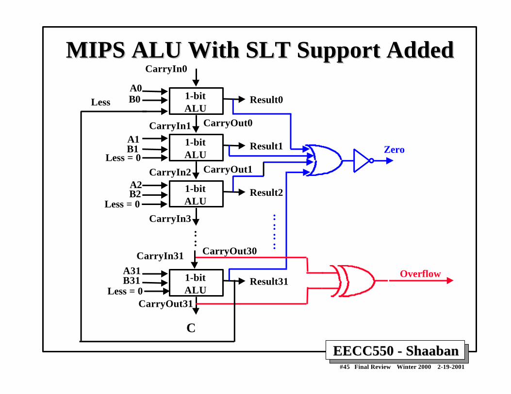
MIPS ALU With SLT Support AddedMIPS ALU With SLT Support Added
A311-bitALU
B31 Result31
B0 1-bitALU
A0Result0
CarryIn0
CarryOut0
A1B1
1-bitALU
Result1
CarryIn1
CarryOut1
A2B2 1-bit
ALUResult2
CarryIn2
CarryIn3
CarryOut31
::
CarryOut30CarryIn31
C
::::
Zero
Overflow
Less = 0
Less = 0
Less = 0
Less

EECC550 - ShaabanEECC550 - Shaaban#46 Final Review Winter 2000 2-19-2001
Improving ALU Performance:Carry Look Ahead (CLA)
A B C-out0 0 0 “kill”0 1 C-in “propagate”1 0 C-in “propagate”1 1 1 “generate”
A0
B1
SGP
G = A and BP = A xor B
A
B
SGP
A
B
SGP
A
B
SGP
Cin
C1 =G0 + C0 • P0
C2 = G1 + G0 • P1 + C0 • P0 • P1
C3 = G2 + G1 C3 = G2 + G1 • • • • P2 + G0 P2 + G0 •••• P1 P1 •••• P2 + C0 P2 + C0 •••• P0 P0 •••• P1 P1 •••• P2 P2
GP
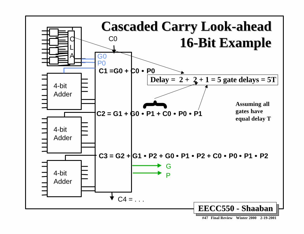
EECC550 - ShaabanEECC550 - Shaaban#47 Final Review Winter 2000 2-19-2001
Cascaded Carry Look-aheadCascaded Carry Look-ahead16-Bit Example16-Bit ExampleC
LA
4-bitAdder
4-bitAdder
4-bitAdder
C1 =G0 + C0 •• P0
C2 = G1 + G0 • • P1 + C0 •• P0 •• P1
C3 = G2 + G1 • • P2 + G0 •• P1 •• P2 + C0 •• P0 •• P1 •• P2GP
G0P0
C4 = . . .
C0
Delay = 2 + 2 + 1 = 5 gate delays = 5T
Assuming allgates haveequal delay T
{

EECC550 - ShaabanEECC550 - Shaaban#48 Final Review Winter 2000 2-19-2001
Unsigned Multiplication ExampleUnsigned Multiplication Example• Paper and pencil example (unsigned):
Multiplicand 1000 Multiplier 1001
1000 0000 0000
1000Product 01001000
• m bits x n bits = m + n bit product, m = 32, n = 32, 64 bit product.
• The binary number system simplifies multiplication:
0 => place 0 ( 0 x multiplicand).
1 => place a copy ( 1 x multiplicand).
• We will examine 4 versions of multiplication hardware & algorithm:
–Successive refinement of design.

EECC550 - ShaabanEECC550 - Shaaban#49 Final Review Winter 2000 2-19-2001
Operation of Operation of CombinationalCombinational Multiplier Multiplier
B0
A0A1A2A3
A0A1A2A3
A0A1A2A3
A0A1A2A3
B1
B2
B3
P0P1P2P3P4P5P6P7
0 0 0 00 0 0
• At each stage shift A left ( x 2).
• Use next bit of B to determine whether to add in shifted multiplicand.
• Accumulate 2n bit partial product at each stage.

EECC550 - ShaabanEECC550 - Shaaban#50 Final Review Winter 2000 2-19-2001
MULTIPLY HARDWARE Version 3MULTIPLY HARDWARE Version 3
Product (Multiplier)
Multiplicand
32-bit ALU
WriteControl
32 bits
64 bits
Shift Right
• Combine Multiplier register and Product register:
– 32-bit Multiplicand register.
– 32 -bit ALU.
– 64-bit Product register, (0-bit Multiplier register).

EECC550 - ShaabanEECC550 - Shaaban#51 Final Review Winter 2000 2-19-2001
Multiply AlgorithmMultiply AlgorithmVersion 3Version 3
DoneYes: 32 repetitions
2. Shift the Product register right 1 bit.
No: < 32 repetitions
1. TestProduct0
Product0 = 0Product0 = 1
1a. Add multiplicand to the left half of product & place the result in the left half of Product register
32nd repetition?
Start

EECC550 - ShaabanEECC550 - Shaaban#52 Final Review Winter 2000 2-19-2001
CombinationalCombinational Shifter from Shifter from MUXes MUXes
1 0sel
A B
D
Basic Building Block
8-bit right shifter
1 0 1 0 1 0 1 0 1 0 1 0 1 0 1 0
1 0 1 0 1 0 1 0 1 0 1 0 1 0 1 0
1 0 1 0 1 0 1 0 1 0 1 0 1 0 1 0
S2 S1 S0A0A1A2A3A4A5A6A7
R0R1R2R3R4R5R6R7
• What comes in the MSBs?
• How many levels for 32-bit shifter?

EECC550 - ShaabanEECC550 - Shaaban#53 Final Review Winter 2000 2-19-2001
DivisionDivision 1001 Quotient
Divisor 1000 1001010 Dividend–1000 10 101 1010 –1000 10 Remainder (or Modulo result)
• See how big a number can be subtracted, creating quotient bit on each step:
Binary => 1 * divisor or 0 * divisor
Dividend = Quotient x Divisor + Remainder => | Dividend | = | Quotient | + | Divisor |
• 3 versions of divide, successive refinement

EECC550 - ShaabanEECC550 - Shaaban#54 Final Review Winter 2000 2-19-2001
Remainder (Quotient)
Divisor
32-bit ALU
WriteControl
32 bits
64 bits
Shift Left“HI” “LO”
• 32-bit Divisor register.
• 32 -bit ALU.
• 64-bit Remainder regegister (0-bit Quotient register).
DIVIDE HARDWARE Version 3DIVIDE HARDWARE Version 3

EECC550 - ShaabanEECC550 - Shaaban#55 Final Review Winter 2000 2-19-2001
3b. Restore the original value by adding the Divisor register to the left half of the Remainderregister, &place the sum in the left half of the Remainder register. Also shift the Remainder register to the left, setting the new least significant bit to 0.
Test Remainder
Remainder < 0Remainder >= 0
2. Subtract the Divisor register from the left half of the Remainder register, & place the result in the left half of the Remainder register.
3a. Shift the Remainder register to the left setting the new rightmost bit to 1.
1. Shift the Remainder register left 1 bit.
Done. Shift left half of Remainder right 1 bit.
Yes: n repetitions (n = 4 here)
nthrepetition?
No: < n repetitions
Start: Place Dividend in RemainderDivide Algorithm Divide Algorithm Version 3Version 3

EECC550 - ShaabanEECC550 - Shaaban#56 Final Review Winter 2000 2-19-2001
Representation of Floating Point Numbers inRepresentation of Floating Point Numbers in
Single PrecisionSingle Precision IEEE 754 StandardIEEE 754 Standard
Example: 0 = 0 00000000 0 . . . 0 -1.5 = 1 01111111 10 . . . 0
Magnitude of numbers that can be represented is in the range: 2
-126(1.0) to 2
127 (2 - 2-23 )
Which is approximately: 1.8 x 10- 38 to 3.40 x 10 38
0 < E < 255Actual exponent is: e = E - 127
1 8 23sign
exponent:excess 127binary integeradded
mantissa:sign + magnitude, normalizedbinary significand with a hidden integer bit: 1.M
E MS
Value = N = (-1)S X 2 E-127 X (1.M)

EECC550 - ShaabanEECC550 - Shaaban#57 Final Review Winter 2000 2-19-2001
Representation of Floating Point Numbers inRepresentation of Floating Point Numbers in
Single PrecisionSingle Precision IEEE 754 StandardIEEE 754 Standard
Example: 0 = 0 00000000 0 . . . 0 -1.5 = 1 01111111 10 . . . 0
Magnitude of numbers that can be represented is in the range: 2
-126(1.0) to 2
127 (2 - 2-23 )
Which is approximately: 1.8 x 10- 38 to 3.40 x 10 38
0 < E < 255Actual exponent is: e = E - 127
1 8 23sign
exponent:excess 127binary integeradded
mantissa:sign + magnitude, normalizedbinary significand with a hidden integer bit: 1.M
E MS
Value = N = (-1)S X 2 E-127 X (1.M)

EECC550 - ShaabanEECC550 - Shaaban#58 Final Review Winter 2000 2-19-2001
Representation of Floating Point Numbers inRepresentation of Floating Point Numbers in
Double PrecisionDouble Precision IEEE 754 StandardIEEE 754 Standard
Example: 0 = 0 00000000000 0 . . . 0 -1.5 = 1 01111111111 10 . . . 0
Magnitude of numbers that can be represented is in the range: 2
-1022 (1.0) to 2
1023 (2 - 2 - 52 )
Which is approximately: 2.23 x 10- 308 to 1.8 x 10 308
0 < E < 2047Actual exponent is: e = E - 1023
1 11 52sign
exponent:excess 1023binary integeradded
Mantissa:sign + magnitude, normalizedbinary significand with a hidden integer bit: 1.M
E MS
Value = N = (-1)S X 2 E-1023 X (1.M)

EECC550 - ShaabanEECC550 - Shaaban#59 Final Review Winter 2000 2-19-2001
Floating Point Conversion ExampleFloating Point Conversion Example• The decimal number -2345.12510 is to be represented in the
IEEE 754 32-bit single precision format:
-2345.12510 = -100100101001.0012 (converted to binary)
= -1.00100101001001 x 211 (normalized binary)
• The mantissa is negative so the sign S is given by:
S = 1
• The biased exponent E is given by E = e + 127
E = 11 + 127 = 13810 = 100010102
• Fractional part of mantissa M:
M = .00100101001001000000000 (in 23 bits)
The IEEE 754 single precision representation is given by:
1 10001010 00100101001001000000000
S E M
1 bit 8 bits 23 bits
Hidden

EECC550 - ShaabanEECC550 - Shaaban#60 Final Review Winter 2000 2-19-2001
Floating PointFloating Point Addition Addition Flowchart Flowchart
Start
Normalize the sum, either shifting right andincrementing the exponent or shifting leftand decrementing the exponent
Compare the exponents of the two numbersshift the smaller number to the right until itsexponent matches the larger exponent
Round the significand to the appropriate number of bitsIf mantissa = 0, set exponent to 0
Add the significands (mantissas)
Done
Overflow orUnderflow ?
Generate exception or return error
(1)
(2)
(3)
(4)
(5)
Stillnormalized?
Yes
No
yes
No

EECC550 - ShaabanEECC550 - Shaaban#61 Final Review Winter 2000 2-19-2001
Floating Point Addition Hardware

EECC550 - ShaabanEECC550 - Shaaban#62 Final Review Winter 2000 2-19-2001
Overflow or Underflow?
Floating PointFloating PointMultiplication FlowchartMultiplication Flowchart
(1)
(2)
(3)
(5)
(6)
Start
Done
Is one/both operands =0?
Set the result to zero: exponent = 0
Multiply the mantissas
Compute sign of result: Xs XOR Ys
Round or truncate the result mantissa
Compute exponent: biased exp.(X) + biased exp.(Y) - bias
Generate exception or return error
Normalize mantissa if needed
(4)
StillNormalized?
(7)
Yes
NoNo
Yes

EECC550 - ShaabanEECC550 - Shaaban#63 Final Review Winter 2000 2-19-2001
Extra Bits for RoundingExtra Bits for RoundingExtra bits used to prevent or minimize rounding errors.
How many extra bits?
IEEE: As if computed the result exactly and rounded.
Addition:
1.xxxxx 1.xxxxx 1.xxxxx
+ 1.xxxxx 0.001xxxxx 0.01xxxxx
1x.xxxxy 1.xxxxxyyy 1x.xxxxyyy
post-normalization pre-normalization pre and post
• Guard Digits: digits to the right of the first p digits of significand to guardagainst loss of digits – can later be shifted left into first P places duringnormalization.
• Addition: carry-out shifted in
• Subtraction: borrow digit and guard
• Multiplication: carry and guard, Division requires guard

EECC550 - ShaabanEECC550 - Shaaban#64 Final Review Winter 2000 2-19-2001
Rounding DigitsRounding DigitsNormalized result, but some non-zero digits to the right of the significand --> the number should be rounded
E.g., B = 10, p = 3: 0 2 1.69
0 0 7.85
0 2 1.61
= 1.6900 * 10
= - .0785 * 10
= 1.6115 * 10
2-bias
2-bias
2-bias-
One round digit must be carried to the right of the guard digit so thatafter a normalizing left shift, the result can be rounded, accordingto the value of the round digit.
IEEE Standard: four rounding modes: round to nearest (default)
round towards plus infinityround towards minus infinityround towards 0
round to nearest: round digit < B/2 then truncate > B/2 then round up (add 1 to ULP: unit in last place) = B/2 then round to nearest even digit
it can be shown that this strategy minimizes the mean error introduced by rounding.

EECC550 - ShaabanEECC550 - Shaaban#65 Final Review Winter 2000 2-19-2001
Sticky BitSticky BitAdditional bit to the right of the round digit to better fine tune rounding
d0 . d1 d2 d3 . . . dp-1 0 0 0 0 . 0 0 X . . . X X X S X X S
Sticky bit: set to 1 if any 1 bits fall off the end of the round digit
d0 . d1 d2 d3 . . . dp-1 0 0 0 0 . 0 0 X . . . X X X 0
d0 . d1 d2 d3 . . . dp-1 0 0 0 0 . 0 0 X . . . X X X 1
generates a borrow
Rounding Summary:
Radix 2 minimizes wobble in precision.
Normal operations in +,-,*,/ require one carry/borrow bit + one guard digit.
One round digit needed for correct rounding.
Sticky bit needed when round digit is B/2 for max accuracy.
Rounding to nearest has mean error = 0 if uniform distribution of digitsare assumed.

EECC550 - ShaabanEECC550 - Shaaban#66 Final Review Winter 2000 2-19-2001
Pipelining: Design GoalsPipelining: Design Goals• The length of the machine clock cycle is determined by the time
required for the slowest pipeline stage.
• An important pipeline design consideration is to balance thelength of each pipeline stage.
• If all stages are perfectly balanced, then the time perinstruction on a pipelined machine (assuming ideal conditionswith no stalls):
Time per instruction on unpipelined machine Number of pipe stages
• Under these ideal conditions:– Speedup from pipelining = the number of pipeline stages = k
– One instruction is completed every cycle: CPI = 1 .

EECC550 - ShaabanEECC550 - Shaaban#67 Final Review Winter 2000 2-19-2001
Pipelined Instruction ProcessingPipelined Instruction ProcessingRepresentationRepresentation
Clock cycle Number Time in clock cycles →Instruction Number 1 2 3 4 5 6 7 8 9
Instruction I IF ID EX MEM WB
Instruction I+1 IF ID EX MEM WB
Instruction I+2 IF ID EX MEM WB
Instruction I+3 IF ID EX MEM WB
Instruction I +4 IF ID EX MEM WB
Time to fill the pipeline
Pipeline Stages:
IF = Instruction Fetch
ID = Instruction Decode
EX = Execution
MEM = Memory Access
WB = Write Back
First instruction, ICompleted
Last instruction, I+4 completed

EECC550 - ShaabanEECC550 - Shaaban#68 Final Review Winter 2000 2-19-2001
For 1000 instructions, execution time:
• Single Cycle Machine:
– 8 ns/cycle x 1 CPI x 1000 inst = 8000 ns
• Multicycle Machine:
– 2 ns/cycle x 4.6 CPI (due to inst mix) x 1000 inst = 9200 ns
• Ideal pipelined machine, 5-stages:
– 2 ns/cycle x (1 CPI x 1000 inst + 4 cycle fill) = 2008 ns
Single Cycle, Multi-Cycle, Pipeline:Single Cycle, Multi-Cycle, Pipeline:Performance Comparison ExamplePerformance Comparison Example

EECC550 - ShaabanEECC550 - Shaaban#69 Final Review Winter 2000 2-19-2001
Single Cycle, Multi-Cycle, Vs. PipelineSingle Cycle, Multi-Cycle, Vs. Pipeline
Clk
Cycle 1
Multiple Cycle Implementation:
IF ID EX MEM WB
Cycle 2 Cycle 3 Cycle 4 Cycle 5 Cycle 6 Cycle 7 Cycle 8 Cycle 9 Cycle 10
IF ID EX MEM
Load Store
Clk
Single Cycle Implementation:
Load Store Waste
IF
R-type
Load IF ID EX MEM WB
Pipeline Implementation:
IF ID EX MEM WBStore
IF ID EX MEM WBR-type
Cycle 1 Cycle 2
8 ns
2ns

EECC550 - ShaabanEECC550 - Shaaban#70 Final Review Winter 2000 2-19-2001
MIPS: A Pipelined DatapathMIPS: A Pipelined Datapath
Instructionmemory
Address
4
32
0
Add Addresult
Shiftleft 2
Ins t
ruct
ion
IF/ID EX/MEM MEM/WB
Mux
0
1
Add
PC
0
Address
Wri tedata
Mux
1Registers
Readdata 1
Readdata 2
Readregister 1
Readregister 2
16Sign
extend
Writeregister
Writedata
Readdata
Datamemory
1
ALUresult
Mux
ALUZero
ID/EX
IF ID EX MEM WBInstruction Fetch Instruction Decode Execution Memory Write Back

EECC550 - ShaabanEECC550 - Shaaban#71 Final Review Winter 2000 2-19-2001
Pipeline ControlPipeline Control• Pass needed control signals along from one stage to the next as the
instruction travels through the pipeline just like the data
Execution/Address Calculation stage control lines
Memory access stage control lines
Write-back stage control
lines
InstructionReg Dst
ALU Op1
ALU Op0
ALU Src Branch
Mem Read
Mem Write
Reg write
Mem to Reg
R-format 1 1 0 0 0 0 0 1 0lw 0 0 0 1 0 1 0 1 1sw X 0 0 1 0 0 1 0 Xbeq X 0 1 0 1 0 0 0 X
Control
EX
M
WB
M
WB
WB
IF/ID ID/EX EX/MEM MEM/WB
Instruction

EECC550 - ShaabanEECC550 - Shaaban#72 Final Review Winter 2000 2-19-2001
Basic Performance Issues In PipeliningBasic Performance Issues In Pipelining• Pipelining increases the CPU instruction throughput: The number of instructions completed per unit time. Under ideal condition instruction throughput is one instruction per machine cycle, or CPI = 1
• Pipelining does not reduce the execution time of anindividual instruction: The time needed to complete allprocessing steps of an instruction (also called instructioncompletion latency).
• It usually slightly increases the execution time of eachinstruction over unpipelined implementations due to theincreased control overhead of the pipeline and pipelinestage registers delays.

EECC550 - ShaabanEECC550 - Shaaban#73 Final Review Winter 2000 2-19-2001
Pipelining Performance ExamplePipelining Performance Example• Example: For an unpipelined machine:
– Clock cycle = 10ns, 4 cycles for ALU operations and branches and 5 cycles formemory operations with instruction frequencies of 40%, 20% and 40%,respectively.
– If pipelining adds 1ns to the machine clock cycle then the speedup ininstruction execution from pipelining is:
Non-pipelined Average instruction execution time = Clock cycle x Average CPI
= 10 ns x ((40% + 20%) x 4 + 40%x 5) = 10 ns x 4.4 = 44 ns
In the pipelined five implementation five stages are used withan average instruction execution time of: 10 ns + 1 ns = 11 ns
Speedup from pipelining = Instruction time unpipelined
Instruction time pipelined
= 44 ns / 11 ns = 4 times

EECC550 - ShaabanEECC550 - Shaaban#74 Final Review Winter 2000 2-19-2001
Pipeline HazardsPipeline Hazards• Hazards are situations in pipelining which prevent the next
instruction in the instruction stream from executing duringthe designated clock cycle resulting in one or more stall cycles.
• Hazards reduce the ideal speedup gained from pipelining andare classified into three classes:
– Structural hazards: Arise from hardware resource conflictswhen the available hardware cannot support all possiblecombinations of instructions.
– Data hazards: Arise when an instruction depends on theresults of a previous instruction in a way that is exposed bythe overlapping of instructions in the pipeline.
– Control hazards: Arise from the pipelining of conditionalbranches and other instructions that change the PC.
EECC550 - ShaabanEECC550 - Shaaban#75 Final Review Winter 2000 2-19-2001
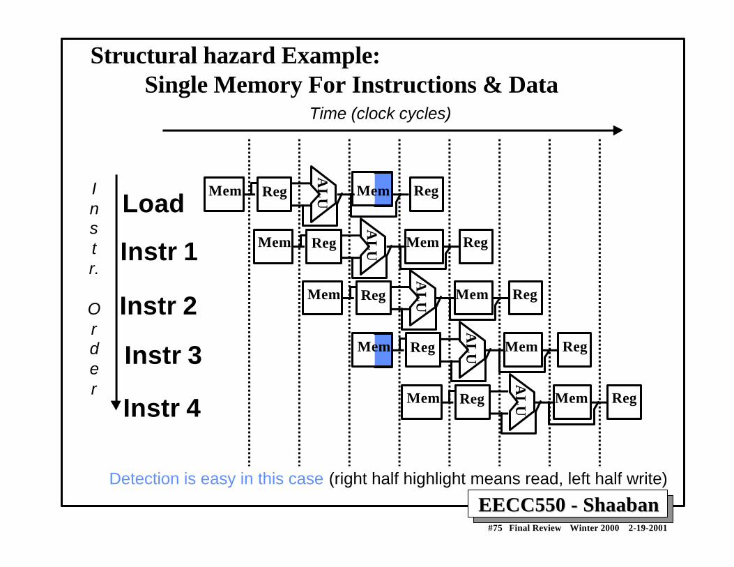
Structural hazard Example: Single Memory For Instructions & Data
Mem
Instr.
Order
Time (clock cycles)
Load
Instr 1
Instr 2
Instr 3
Instr 4A
LUMem Reg Mem Reg
AL
UMem Reg Mem Reg
AL
UMem Reg Mem Reg
AL
UReg Mem Reg
AL
UMem Reg Mem Reg
Detection is easy in this case (right half highlight means read, left half write)

EECC550 - ShaabanEECC550 - Shaaban#76 Final Review Winter 2000 2-19-2001
Data Hazards ExampleData Hazards Example• Problem with starting next instruction before first is
finished
– Data dependencies here that “go backward in time”create data hazards.
sub $2, $1, $3and $12, $2, $5or $13, $6, $2add $14, $2, $2sw $15, 100($2)
IM Reg
IM Reg
CC 1 CC 2 CC 3 CC 4 CC 5 CC 6
Time (in clock cycles)
sub $2, $1, $3
Programexecutionorder(in instructions)
and $12, $2, $5
IM Reg DM Reg
IM DM Reg
IM DM Reg
CC 7 CC 8 CC 9
10 10 10 10 10/–20 –20 –20 – 20 – 20
or $13, $6, $2
add $14, $2, $2
sw $15, 100($2)
Value of register $2:
DM Reg
Reg
Reg
Reg
DM

EECC550 - ShaabanEECC550 - Shaaban#77 Final Review Winter 2000 2-19-2001
Data Hazard Resolution: Stall CyclesData Hazard Resolution: Stall CyclesStall the pipeline by a number of cycles.The control unit must detect the need to insert stall cycles.
In this case two stall cycles are needed.
IM Reg
IM
CC 1 CC 2 CC 3 CC 4 CC 5 CC 6
Time (in clock cycles)
sub $2, $1, $3
Programexecutionorder(in instructions)
and $12, $2, $5
CC 7 CC 8
10 10 10 10 10/– 20 – 20 – 20 – 20
CC 9
– 20
or $13, $6, $2
add $14, $2, $2
sw $15, 100($2)
Value of register $2:
DM Reg
Reg
IM Reg DM Reg
IM DM Reg
IM DM Reg
Reg
Reg
Reg
DMSTALL STALL
CC 10
– 20
CC 11
– 20
STALL STALL

EECC550 - ShaabanEECC550 - Shaaban#78 Final Review Winter 2000 2-19-2001
Data Hazard Resolution: Stall CyclesData Hazard Resolution: Stall CyclesStall the pipeline by a number of cycles.The control unit must detect the need to insert stall cycles.
In this case two stall cycles are needed.
IM Reg
IM
CC 1 CC 2 CC 3 CC 4 CC 5 CC 6
Time (in clock cycles)
sub $2, $1, $3
Programexecutionorder(in instructions)
and $12, $2, $5
CC 7 CC 8
10 10 10 10 10/– 20 – 20 – 20 – 20
CC 9
– 20
or $13, $6, $2
add $14, $2, $2
sw $15, 100($2)
Value of register $2:
DM Reg
Reg
IM Reg DM Reg
IM DM Reg
IM DM Reg
Reg
Reg
Reg
DMSTALL STALL
CC 10
– 20
CC 11
– 20
STALL STALL
EECC550 - ShaabanEECC550 - Shaaban#79 Final Review Winter 2000 2-19-2001
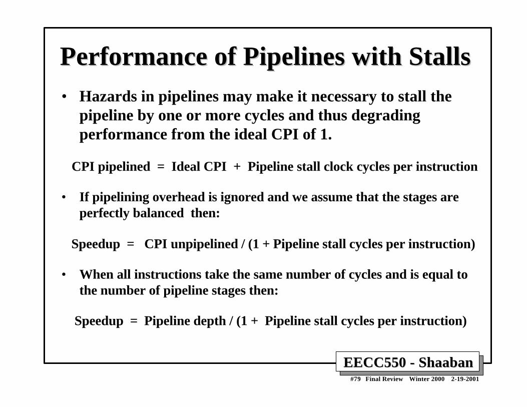
Performance of Pipelines with StallsPerformance of Pipelines with Stalls• Hazards in pipelines may make it necessary to stall the
pipeline by one or more cycles and thus degradingperformance from the ideal CPI of 1.
CPI pipelined = Ideal CPI + Pipeline stall clock cycles per instruction
• If pipelining overhead is ignored and we assume that the stages areperfectly balanced then:
Speedup = CPI unpipelined / (1 + Pipeline stall cycles per instruction)
• When all instructions take the same number of cycles and is equal tothe number of pipeline stages then:
Speedup = Pipeline depth / (1 + Pipeline stall cycles per instruction)

EECC550 - ShaabanEECC550 - Shaaban#80 Final Review Winter 2000 2-19-2001
Data Hazard Resolution: ForwardingData Hazard Resolution: Forwarding– Register file forwarding to handle read/write to same register
– ALU forwarding

EECC550 - ShaabanEECC550 - Shaaban#81 Final Review Winter 2000 2-19-2001
Data Hazard Example With ForwardingData Hazard Example With Forwarding
IM Reg
IM Reg
CC 1 CC 2 CC 3 CC 4 CC 5 CC 6
Time (in clock cycles)
sub $2, $1, $3
Programexecution order(in instructions)
and $12, $2, $5
IM Reg DM Reg
IM DM Reg
IM DM Reg
CC 7 CC 8 CC 9
10 10 10 10 10/– 20 – 20 – 20 –20 –20
or $13, $6, $2
add $14, $2, $2
sw $15, 100($2)
Value of register $2 :
DM Reg
Reg
Reg
Reg
X X X –20 X X X X XValue of EX/MEM :X X X X – 20 X X X XValue of MEM/WB :
DM

EECC550 - ShaabanEECC550 - Shaaban#82 Final Review Winter 2000 2-19-2001
A Data Hazard Requiring A StallA Data Hazard Requiring A Stall
Reg
IM
Reg
Reg
IM
CC 1 CC 2 CC 3 CC 4 CC 5 CC 6
Time (in clock cycles)
lw $2, 20($1)
Programexecutionorder(in instructions)
and $4, $2, $5
IM Reg DM Reg
IM DM Reg
IM DM Reg
CC 7 CC 8 CC 9
or $8, $2, $6
add $9, $4, $2
slt $1, $6, $7
DM Reg
Reg
Reg
DM
A load followed by an R-type instruction that uses the loaded value
Even with forwarding in place a stall cycle is neededThis condition must be detected by hardware

EECC550 - ShaabanEECC550 - Shaaban#83 Final Review Winter 2000 2-19-2001
Compiler Scheduling ExampleCompiler Scheduling Example• Reorder the instructions to avoid as many pipeline stalls as possible:
lw $15, 0($2)lw $16, 4($2)sw $16, 0($2)sw $15, 4($2)
• The data hazard occurs on register $16 between the second lw and the first swresulting in a stall cycle
• With forwarding we need to find only one independent instructions to placebetween them, swapping the lw instructions works:
lw $15, 0($2)lw $16, 4($2)nopnopsw $15, 0($2)sw $16, 4($2)
• Without forwarding we need three independent instructions to place betweenthem, so in addition two nops are added.
lw $15, 0($2)lw $16, 4($2)sw $15, 0($2)sw $16, 4($2)

EECC550 - ShaabanEECC550 - Shaaban#84 Final Review Winter 2000 2-19-2001
Control Hazards: ExampleControl Hazards: Example• Three other instructions are in the pipeline before branch
instruction target decision is made when BEQ is in MEM stage.
• In the above diagram, we are predicting “branch not taken”– Need to add hardware for flushing the three following instructions if
we are wrong losing three cycles.
Reg
Reg
CC 1
Time (in clock cycles)
40 beq $1, $3, 7
Programexecutionorder(in instructions)
IM Reg
IM DM
IM DM
IM DM
DM
DM Reg
Reg Reg
Reg
Reg
RegIM
44 and $12, $2, $5
48 or $13, $6, $2
52 add $14, $2, $2
72 lw $4, 50($7)
CC 2 CC 3 CC 4 CC 5 CC 6 CC 7 CC 8 CC 9
Reg

EECC550 - ShaabanEECC550 - Shaaban#85 Final Review Winter 2000 2-19-2001
Reducing Delay of Taken BranchesReducing Delay of Taken Branches• Next PC of a branch known in MEM stage: Costs three lost cycles if taken.• If next PC is known in EX stage, one cycle is saved.• Branch address calculation can be moved to ID stage using a register comparator, costing
only one cycle if branch is taken.
PCInstruc tion
m emory
4
R egisters
Mux
Mux
Mux
ALU
EX
M
WB
M
WB
WB
ID/EX
0
EX/MEM
MEM/WB
Datamemory
Mux
H azarddetection
unit
Forw ardingunit
IF.Flush
IF/ID
Signextend
C ontrol
Mux
=
Shif tlef t 2
Mux

EECC550 - ShaabanEECC550 - Shaaban#86 Final Review Winter 2000 2-19-2001
Pipeline Performance ExamplePipeline Performance Example• Assume the following MIPS instruction mix:
• What is the resulting CPI for the pipelined MIPS withforwarding and branch address calculation in ID stage?
• CPI = Ideal CPI + Pipeline stall clock cycles per instruction
= 1 + stalls by loads + stalls by branches
= 1 + .3x.25x1 + .2 x .45x1
= 1 + .075 + .09
= 1.165
Type FrequencyArith/Logic 40%Load 30% of which 25% are followed immediately by an instruction using the loaded valueStore 10%branch 20% of which 45% are taken

EECC550 - ShaabanEECC550 - Shaaban#87 Final Review Winter 2000 2-19-2001
Memory Hierarchy: MotivationMemory Hierarchy: MotivationProcessor-Memory (DRAM) Performance GapProcessor-Memory (DRAM) Performance Gap
µProc60%/yr.
DRAM7%/yr.
1
10
100
100019
8019
81
1983
1984
1985
1986
1987
1988
1989
1990
1991
1992
1993
1994
1995
1996
1997
1998
1999
2000
DRAM
CPU
1982
Processor-MemoryPerformance Gap:(grows 50% / year)
Per
form
ance

EECC550 - ShaabanEECC550 - Shaaban#88 Final Review Winter 2000 2-19-2001
Processor-DRAM Performance Gap Impact:Processor-DRAM Performance Gap Impact:
Example Example
• To illustrate the performance impact, assume a pipelined RISCCPU with CPI = 1 using non-ideal memory.
• Over an 10 year period, ignoring other factors, the cost of a fullmemory access in terms of number of wasted instructions:
CPU CPU Memory Minimum CPU cycles or Year speed cycle Access instructions wasted MHZ ns ns
1986: 8 125 190 190/125 = 1.51988: 33 30 175 175/30 = 5.81991: 75 13.3 155 155/13.3 = 11.651994: 200 5 130 130/5 = 261996: 300 3.33 100 110/3.33 = 33

EECC550 - ShaabanEECC550 - Shaaban#89 Final Review Winter 2000 2-19-2001
Memory Hierarchy: MotivationMemory Hierarchy: Motivation
The Principle Of LocalityThe Principle Of Locality• Programs usually access a relatively small portion of their
address space (instructions/data) at any instant of time(program working set).
• Two Types of locality:
– Temporal Locality: If an item is referenced, it will tend tobe referenced again soon.
– Spatial locality: If an item is referenced, items whoseaddresses are close will tend to be referenced soon.
• The presence of locality in program behavior, makes itpossible to satisfy a large percentage of program access needsusing memory levels with much less capacity than programaddress space.

EECC550 - ShaabanEECC550 - Shaaban#90 Final Review Winter 2000 2-19-2001
Levels of The Memory HierarchyLevels of The Memory Hierarchy
Part of The On-chipCPU Datapath 16-256 Registers
One or more levels (Static RAM):Level 1: On-chip 16-64K Level 2: On or Off-chip 128-512KLevel 3: Off-chip 128K-8M
Registers
Cache
Main Memory
Magnetic Disc
Optical Disk or Magnetic Tape
Farther away from The CPU
Lower Cost/Bit
Higher Capacity
Increased AccessTime/Latency
Lower ThroughputDynamic RAM (DRAM) 16M-16G
Interface:SCSI, RAID, IDE, 13944G-100G

EECC550 - ShaabanEECC550 - Shaaban#91 Final Review Winter 2000 2-19-2001
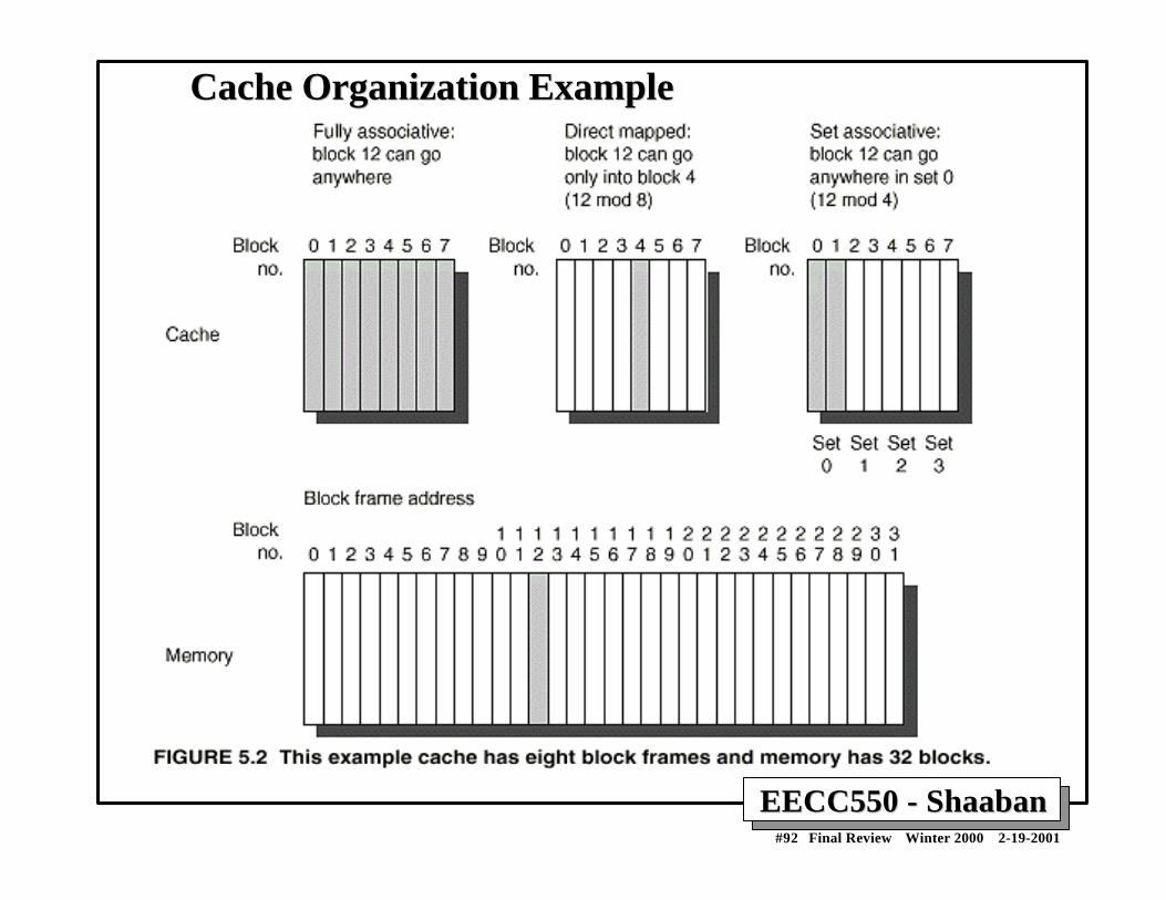
Cache Design & Operation IssuesCache Design & Operation Issues• Q1: Where can a block be placed cache?
(Block placement strategy & Cache organization)– Fully Associative, Set Associative, Direct Mapped
• Q2: How is a block found if it is in cache?(Block identification)– Tag/Block
• Q3: Which block should be replaced on a miss?(Block replacement)– Random, LRU
• Q4: What happens on a write?(Cache write policy)– Write through, write back
EECC550 - ShaabanEECC550 - Shaaban#92 Final Review Winter 2000 2-19-2001
Cache Organization ExampleCache Organization Example

EECC550 - ShaabanEECC550 - Shaaban#93 Final Review Winter 2000 2-19-2001
Locating A Data Block in CacheLocating A Data Block in Cache• Each block frame in cache has an address tag.
• The tags of every cache block that might contain the required dataare checked or searched in parallel.
• A valid bit is added to the tag to indicate whether this entry containsa valid address.
• The address from the CPU to cache is divided into:
– A block address, further divided into:
• An index field to choose a block set in cache.
(no index field when fully associative).
• A tag field to search and match addresses in the selected set.
– A block offset to select the data from the block.
Block Address BlockOffsetTag Index

EECC550 - ShaabanEECC550 - Shaaban#94 Final Review Winter 2000 2-19-2001
Address Field SizesAddress Field Sizes
Block Address BlockOffsetTag Index
Block offset size = log2(block size)
Index size = log2(Total number of blocks/associativity)
Tag size = address size - index size - offset sizeTag size = address size - index size - offset size
Physical Address Generated by CPU

EECC550 - ShaabanEECC550 - Shaaban#95 Final Review Winter 2000 2-19-2001
Four-Way Set Associative Cache:Four-Way Set Associative Cache:MIPS Implementation ExampleMIPS Implementation Example
Address
22 8
V TagIndex
0
1
2
253
254
255
Data V Tag Data V Tag Data V Tag Data
3222
4- to-1 m ultiplexo r
Hit Da ta
123891011123 031 0
IndexField
TagField
256 sets1024 block frames

EECC550 - ShaabanEECC550 - Shaaban#96 Final Review Winter 2000 2-19-2001
Cache Organization/Addressing ExampleCache Organization/Addressing Example
• Given the following:– A single-level L1 cache with 128 cache block frames
• Each block frame contains four words (16 bytes)
– 16-bit memory addresses to be cached (64K bytes main memoryor 4096 memory blocks)
• Show the cache organization/mapping and cacheaddress fields for:
• Fully Associative cache.
• Direct mapped cache.
• 2-way set-associative cache.

EECC550 - ShaabanEECC550 - Shaaban#97 Final Review Winter 2000 2-19-2001
Cache Example: Fully Associative CaseCache Example: Fully Associative Case
Block offset = 4 bits
Block Address = 12 bits
Tag = 12 bits
All 128 tags mustbe checked in parallelby hardware to locate a data block
V
V
V
Valid bit

EECC550 - ShaabanEECC550 - Shaaban#98 Final Review Winter 2000 2-19-2001
Cache Example: Direct Mapped CaseCache Example: Direct Mapped Case
Block offset = 4 bits
Block Address = 12 bits
Tag = 5 bits Index = 7 bits Main Memory
Only a single tag mustbe checked in parallelto locate a data block
V
Valid bit
V
V
V

EECC550 - ShaabanEECC550 - Shaaban#99 Final Review Winter 2000 2-19-2001
Block offset = 4 bits
Block Address = 12 bits
Tag = 6 bits Index = 6 bits
Cache Example: 2-Way Set-AssociativeCache Example: 2-Way Set-Associative
Main Memory
Two tags in a set mustbe checked in parallelto locate a data block
Valid bits not shown

EECC550 - ShaabanEECC550 - Shaaban#100 Final Review Winter 2000 2-19-2001
Cache Replacement PolicyCache Replacement Policy• When a cache miss occurs the cache controller may have to
select a block of cache data to be removed from a cache blockframe and replaced with the requested data, such a block isselected by one of two methods:
– Random:• Any block is randomly selected for replacement providing
uniform allocation.
• Simple to build in hardware.
• The most widely used cache replacement strategy.
– Least-recently used (LRU):• Accesses to blocks are recorded and and the block
replaced is the one that was not used for the longest periodof time.
• LRU is expensive to implement, as the number of blocksto be tracked increases, and is usually approximated.

EECC550 - ShaabanEECC550 - Shaaban#101 Final Review Winter 2000 2-19-2001
Miss Rates for Caches with Different Size,Miss Rates for Caches with Different Size,Associativity & Replacement AlgorithmAssociativity & Replacement Algorithm
Sample DataSample Data
Associativity: 2-way 4-way 8-way
Size LRU Random LRU Random LRU Random
16 KB 5.18% 5.69% 4.67% 5.29% 4.39% 4.96%
64 KB 1.88% 2.01% 1.54% 1.66% 1.39% 1.53%
256 KB 1.15% 1.17% 1.13% 1.13% 1.12% 1.12%

EECC550 - ShaabanEECC550 - Shaaban#102 Final Review Winter 2000 2-19-2001
Single Level Cache PerformanceSingle Level Cache PerformanceFor a CPU with a single level (L1) of cache and no stalls for
cache hits:
CPU time = (CPU execution clock cycles +
Memory stall clock cycles) x clock cycle time
Memory stall clock cycles = (Reads x Read miss rate x Read miss penalty) + (Writes x Write miss rate x Write miss penalty)
If write and read miss penalties are the same:
Memory stall clock cycles = Memory accesses x Miss rate x Miss penalty
With ideal memory

EECC550 - ShaabanEECC550 - Shaaban#103 Final Review Winter 2000 2-19-2001
Single Level Cache PerformanceSingle Level Cache PerformanceCPUtime = IC x CPI x C
CPIexecution = CPI with ideal memory
CPI = CPIexecution + Mem Stall cycles per instruction
CPUtime = IC x (CPIexecution + Mem Stall cycles per instruction) x C
Mem Stall cycles per instruction = Mem accesses per instruction x Miss rate x Miss penalty
CPUtime = IC x (CPIexecution + Mem accesses per instruction x Miss rate x Miss penalty ) x C
Misses per instruction = Memory accesses per instruction x Miss rate
CPUtime = IC x (CPIexecution + Misses per instruction x Miss penalty) x C

EECC550 - ShaabanEECC550 - Shaaban#104 Final Review Winter 2000 2-19-2001
Cache Performance ExampleCache Performance Example• Suppose a CPU executes at Clock Rate = 200 MHz (5 ns per cycle)
with a single level of cache.
• CPIexecution = 1.1
• Instruction mix: 50% arith/logic, 30% load/store, 20% control
• Assume a cache miss rate of 1.5% and a miss penalty of 50 cycles.
CPI = CPIexecution + mem stalls per instruction
Mem Stalls per instruction =
Mem accesses per instruction x Miss rate x Miss penalty
Mem accesses per instruction = 1 + .3 = 1.3
Mem Stalls per instruction = 1.3 x .015 x 50 = 0.975
CPI = 1.1 + .975 = 2.075
The ideal CPU with no misses is 2.075/1.1 = 1.88 times faster
Instruction fetch Load/store

EECC550 - ShaabanEECC550 - Shaaban#105 Final Review Winter 2000 2-19-2001
Cache Performance ExampleCache Performance Example• Suppose for the previous example we double the clock rate to
400 MHZ, how much faster is this machine, assuming similarmiss rate, instruction mix?
• Since memory speed is not changed, the miss penalty takesmore CPU cycles:
Miss penalty = 50 x 2 = 100 cycles.
CPI = 1.1 + 1.3 x .015 x 100 = 1.1 + 1.95 = 3.05
Speedup = (CPIold x Cold)/ (CPInew x Cnew)
= 2.075 x 2 / 3.05 = 1.36
The new machine is only 1.36 times faster rather than 2
times faster due to the increased effect of cache misses.
→ CPUs with higher clock rate, have more cycles per cache miss and more memory impact on CPI

EECC550 - ShaabanEECC550 - Shaaban#106 Final Review Winter 2000 2-19-2001
3 Levels of Cache3 Levels of Cache
CPU
L1 Cache
L2 Cache
L3 Cache
Main Memory
Hit Rate= H1, Hit time = 1 cycle
Hit Rate= H2, Hit time = T2 cycles
Hit Rate= H3, Hit time = T3
Memory access penalty, M

EECC550 - ShaabanEECC550 - Shaaban#107 Final Review Winter 2000 2-19-2001
CPUtime = IC x (CPIexecution + Mem Stall cycles per instruction) x CMem Stall cycles per instruction = Mem accesses per instruction x Stall cycles per access
• For a system with 3 levels of cache, assuming no penaltywhen found in L1 cache:
Stall cycles per memory access =
[miss rate L1] x [ Hit rate L2 x Hit time L2
+ Miss rate L2 x (Hit rate L3 x Hit time L3
+ Miss rate L3 x Memory access penalty) ] =
[1 - H1] x [ H2 x T2
+ ( 1-H2 ) x (H3 x (T2 + T3)
+ (1 - H3) x M) ]
3-Level Cache Performance3-Level Cache Performance

EECC550 - ShaabanEECC550 - Shaaban#108 Final Review Winter 2000 2-19-2001
Three Level Cache ExampleThree Level Cache Example• CPU with CPIexecution = 1.1 running at clock rate = 500 MHZ• 1.3 memory accesses per instruction.• L1 cache operates at 500 MHZ with a miss rate of 5%• L2 cache operates at 250 MHZ with miss rate 3%, (T2 = 2 cycles)• L3 cache operates at 100 MHZ with miss rate 1.5%, (T3 = 5 cycles)
• Memory access penalty, M= 100 cycles. Find CPI.
• With single L1, CPI = 1.1 + 1.3 x .05 x 100 = 7.6CPI = CPIexecution + Mem Stall cycles per instructionMem Stall cycles per instruction = Mem accesses per instruction x Stall cycles per access
Stall cycles per memory access = [1 - H1] x [ H2 x T2 + ( 1-H2 ) x (H3 x (T2 + T3)
+ (1 - H3) x M) ]
= [.05] x [ .97 x 2 + (.03) x ( .985 x (2+5)
+ .015 x 100)]
= .05 x [ 1.94 + .03 x ( 6.895 + 1.5) ]
= .05 x [ 1.94 + .274] = .11
• CPI = 1.1 + 1.3 x .11 = 1.24