Embed Size (px)
Citation preview
cps 104 memory. 1 ©RW Fall 2000
CPS101Computer Or ganization and Pro grammin g
Lecture 13: The Memory System
Robert Wa gner
cps 104 memory. 2 ©RW Fall 2000
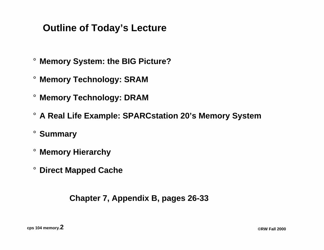
Outline of Today’s Lecture
° Memor y System: the BIG Picture?
° Memor y Technolo gy: SRAM
° Memor y Technolo gy: DRAM
° A Real Life Example: SPARCstation 20’s Memor y System
° Summar y
° Memor y Hierarch y
° Direct Mapped Cache
Chapter 7, Appendix B, pa ges 26-33
cps 104 memory. 3 ©RW Fall 2000
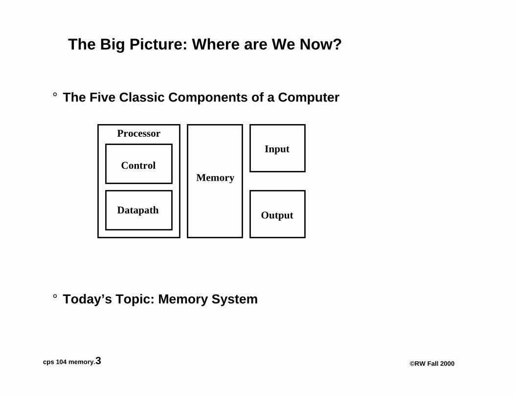
The Bi g Picture: Where are We Now?
° The Five Classic Components of a Computer
° Today’s Topic: Memor y System
Control
Datapath
Memory
Processor
Input
Output
cps 104 memory. 4 ©RW Fall 2000
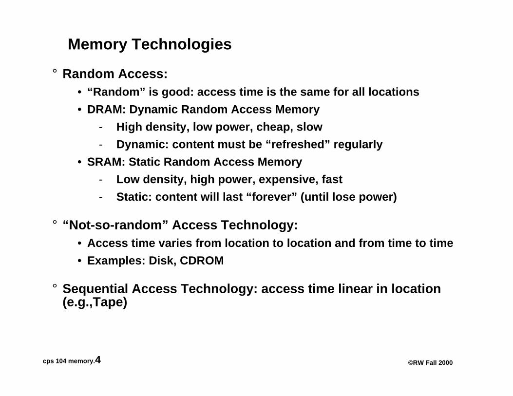
Memory Technolo gies
° Random Access:• “Random” is good: access time is the same for all locations
• DRAM: Dynamic Random Access Memory
- High density, low power, cheap, slow
- Dynamic: content must be “refreshed” regularly
• SRAM: Static Random Access Memory
- Low density, high power, expensive, fast
- Static: content will last “forever” (until lose power)
° “Not-so-random” Access Technolo gy:• Access time varies from location to location and from time to time
• Examples: Disk, CDROM
° Sequential Access Technolo gy: access time linear in location(e.g.,Tape)
cps 104 memory. 5 ©RW Fall 2000
Memory Hierarchy
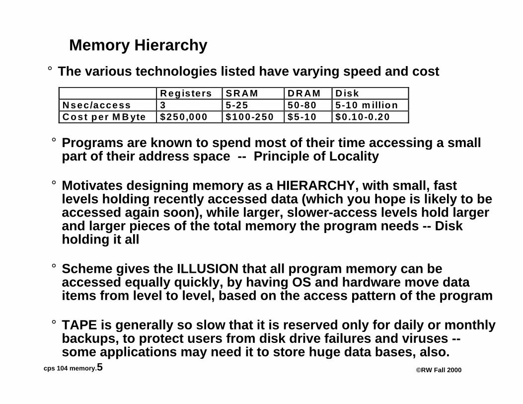
° The various technolo gies listed have var ying speed and cost
R eg is te rs S R AM D R AM D iskN sec/access 3 5-25 50-80 5-10 m illionC os t per M B yte $250,000 $100-250 $5-10 $0.10-0 .20
° Programs are known to spend most of their time accessin g a smallpart of their address space -- Principle of Localit y
° Motivates desi gnin g memor y as a HIERARCHY, with small, fastlevels holdin g recentl y accessed data (which you hope is likel y to beaccessed a gain soon), while lar ger, slower-access levels hold lar gerand lar ger pieces of the total memor y the pro gram needs -- Diskholdin g it all
° Scheme gives the ILLUSION that all pro gram memor y can beaccessed equall y quickl y, by havin g OS and hardware move dataitems from level to level, based on the access pattern of the pro gram
° TAPE is generall y so slow that it is reserved onl y for dail y or monthl ybackups, to protect users from disk drive failures and viruses --some applications ma y need it to store hu ge data bases, also.
cps 104 memory. 6 ©RW Fall 2000
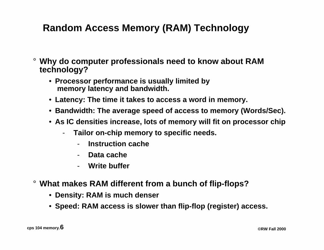
Random Access Memory (RAM) Technolo gy
° Why do computer professionals need to know about RAMtechnolo gy?
• Processor performance is usually limited by memory latency and bandwidth.
• Latency: The time it takes to access a word in memory.
• Bandwidth: The average speed of access to memory (Words/Sec).
• As IC densities increase, lots of memory will fit on processor chip
- Tailor on-chip memory to specific needs.
- Instruction cache
- Data cache
- Write buffer
° What makes RAM different from a bunch of flip-flops?• Density: RAM is much denser
• Speed: RAM access is slower than flip-flop (register) access.
cps 104 memory. 7 ©RW Fall 2000
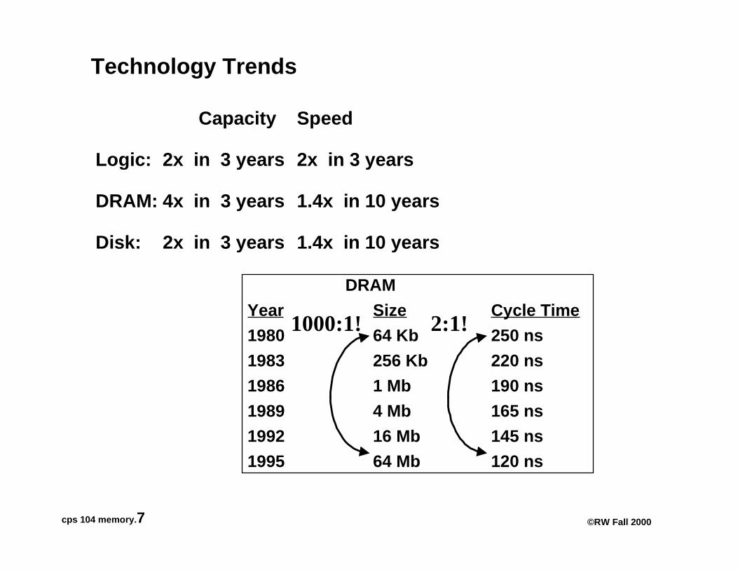
Technolo gy Trends
DRAM
Year Size Cycle Time
1980 64 Kb 250 ns
1983 256 Kb 220 ns
1986 1 Mb 190 ns
1989 4 Mb 165 ns
1992 16 Mb 145 ns
1995 64 Mb 120 ns
Capacit y Speed
Logic: 2x in 3 years 2x in 3 years
DRAM: 4x in 3 years 1.4x in 10 years
Disk: 2x in 3 years 1.4x in 10 years
1000:1! 2:1!
cps 104 memory. 8 ©RW Fall 2000
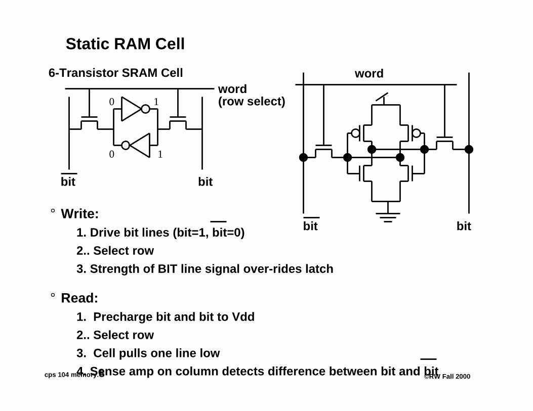
Static RAM Cell
6-Transistor SRAM Cell
bit bit
word(row select)
° Write:1. Drive bit lines (bit=1, bit=0)
2.. Select row
3. Strength of BIT line signal over-rides latch
° Read:1. Precharge bit and bit to Vdd
2.. Select row
3. Cell pulls one line low
4. Sense amp on column detects difference between bit and bit
bit bit
word
10
0 1
cps 104 memory. 9 ©RW Fall 2000
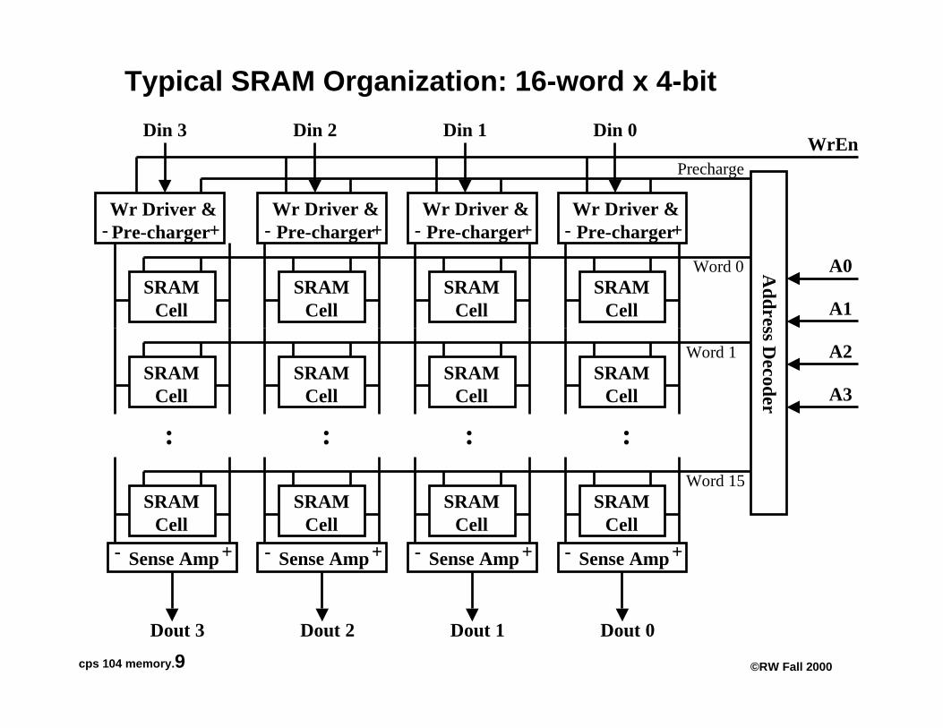
Typical SRAM Or ganization: 16-word x 4-bit
SRAMCell
SRAMCell
SRAMCell
SRAMCell
SRAMCell
SRAMCell
SRAMCell
SRAMCell
SRAMCell
SRAMCell
SRAMCell
SRAMCell
- +Sense Amp - +Sense Amp - +Sense Amp - +Sense Amp
: : : :
Word 0
Word 1
Word 15
Dout 0Dout 1Dout 2Dout 3
- +Wr Driver &Pre-charger - +
Wr Driver &Pre-charger - +
Wr Driver &Pre-charger - +
Wr Driver &Pre-charger
Address D
ecoder
WrEnPrecharge
Din 0Din 1Din 2Din 3
A0
A1
A2
A3
cps 104 memory. 10 ©RW Fall 2000
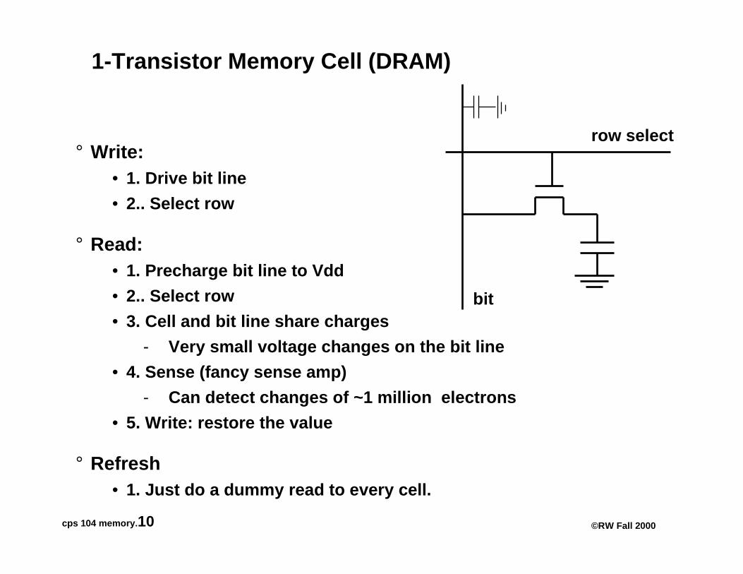
1-Transistor Memory Cell (DRAM)
° Write:• 1. Drive bit line
• 2.. Select row
° Read:• 1. Precharge bit line to Vdd
• 2.. Select row
• 3. Cell and bit line share charges
- Very small voltage changes on the bit line
• 4. Sense (fancy sense amp)
- Can detect changes of ~1 million electrons
• 5. Write: restore the value
° Refresh• 1. Just do a dummy read to every cell.
row select
bit
cps 104 memory. 11 ©RW Fall 2000
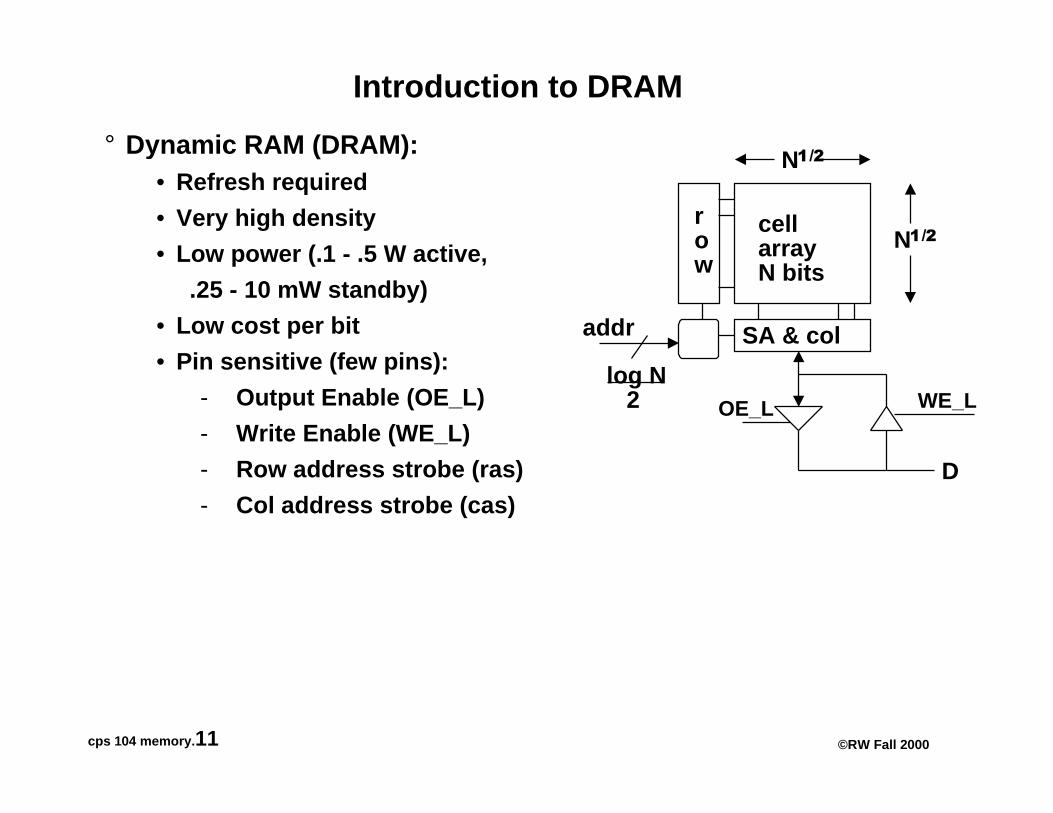
Introduction to DRAM
° Dynamic RAM (DRAM):• Refresh required
• Very high density
• Low power (.1 - .5 W active,
.25 - 10 mW standby)
• Low cost per bit
• Pin sensitive (few pins):
- Output Enable (OE_L)
- Write Enable (WE_L)
- Row address strobe (ras)
- Col address strobe (cas)
cellarrayN bits
N���
N���
row
SA & coladdr
log N 2
D
WE_LOE_L
cps 104 memory. 12 ©RW Fall 2000
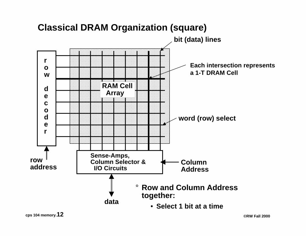
Classical DRAM Or ganization (square)
row
decoder
rowaddress
Sense-Amps, Column Selector & I/O Circuits
ColumnAddress
data
RAM Cell Array
word (row) select
bit (data) lines
° Row and Column Addresstogether:
• Select 1 bit at a time
Each intersection representsa 1-T DRAM Cell
cps 104 memory. 13 ©RW Fall 2000
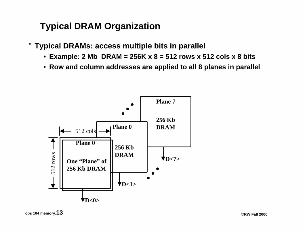
Typical DRAM Or ganization
° Typical DRAMs: access multiple bits in parallel• Example: 2 Mb DRAM = 256K x 8 = 512 rows x 512 cols x 8 bits
• Row and column addresses are applied to all 8 planes in parallel
One “Plane” of256 Kb DRAM
512
ro
ws
Plane 0
512 cols
D<0>
Plane 0
D<1>
Plane 7
D<7>
256 KbDRAM
256 KbDRAM
cps 104 memory. 14 ©RW Fall 2000
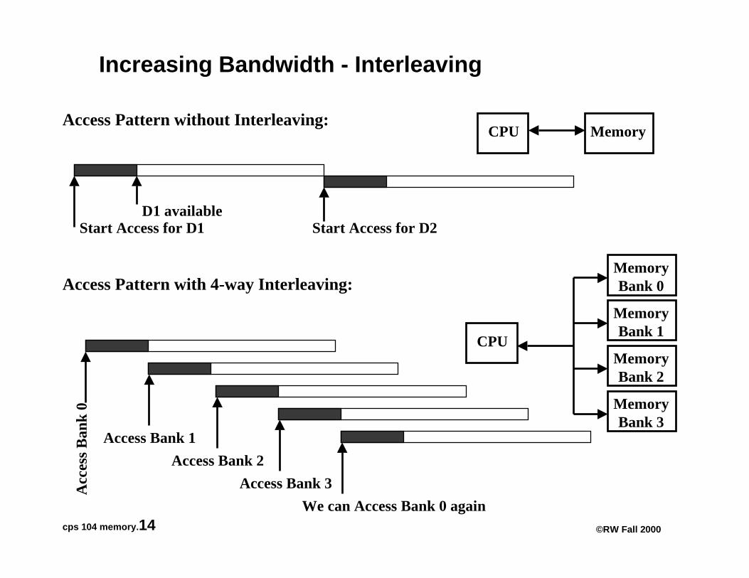
Increasin g Bandwidth - Interleavin g
Access Pattern without Interleaving:
Start Access for D1
CPU Memory
Start Access for D2D1 available
Access Pattern with 4-way Interleaving:
Acc
ess
Ban
k 0
Access Bank 1
Access Bank 2
Access Bank 3
We can Access Bank 0 again
CPU
MemoryBank 1
MemoryBank 0
MemoryBank 3
MemoryBank 2
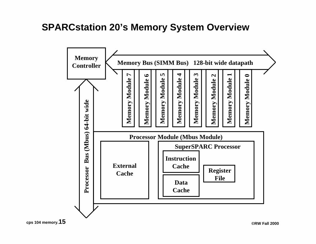
cps 104 memory. 15 ©RW Fall 2000
Memory Bus (SIMM Bus) 128-bit wide datapath
SPARCstation 20’s Memory System Overview
MemoryController
Mem
ory
Mod
ule
0
Pro
cess
or B
us (
Mbu
s) 6
4-bi
t wid
e
Mem
ory
Mod
ule
1
Mem
ory
Mod
ule
2
Mem
ory
Mod
ule
3
Mem
ory
Mod
ule
4
Mem
ory
Mod
ule
5
Mem
ory
Mod
ule
6
Mem
ory
Mod
ule
7Processor Module (Mbus Module)
ExternalCache
SuperSPARC Processor
InstructionCache
DataCache
RegisterFile
cps 104 memory. 16 ©RW Fall 2000
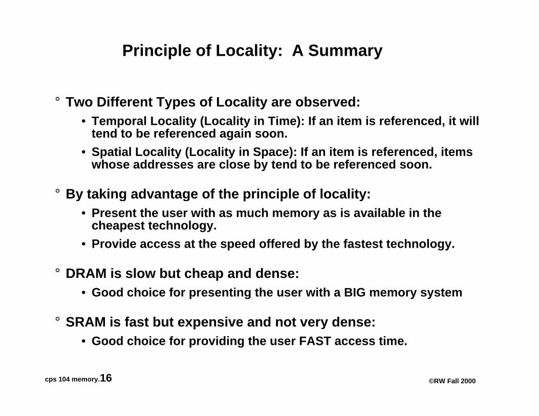
Principle of Locality: A Summary
° Two Different T ypes of Localit y are observed:• Temporal Locality (Locality in Time): If an item is referenced, it will
tend to be referenced again soon.
• Spatial Locality (Locality in Space): If an item is referenced, itemswhose addresses are close by tend to be referenced soon.
° By takin g advanta ge of the principle of localit y:• Present the user with as much memory as is available in the
cheapest technology.
• Provide access at the speed offered by the fastest technology.
° DRAM is slow but cheap and dense:• Good choice for presenting the user with a BIG memory system
° SRAM is fast but expensive and not ver y dense:• Good choice for providing the user FAST access time.
cps 104 memory. 17 ©RW Fall 2000
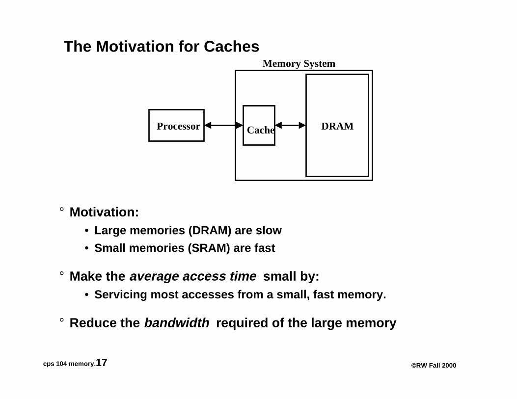
The Motivation for Caches
° Motivation:• Large memories (DRAM) are slow
• Small memories (SRAM) are fast
° Make the average access time small b y:• Servicing most accesses from a small, fast memory.
° Reduce the bandwidth required of the lar ge memor y
Processor
Memory System
Cache DRAM
cps 104 memory. 18 ©RW Fall 2000
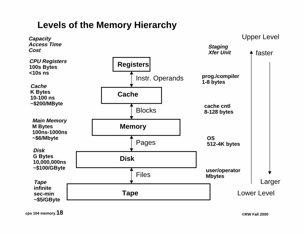
Levels of the Memory Hierarchy
CPU Registers100s Bytes<10s ns
CacheK Bytes10-100 ns~$200/MByte
Main MemoryM Bytes100ns-1000ns~$6/Mbyte
DiskG Bytes10,000,000ns~$100/GByte
CapacityAccess TimeCost
Tapeinfinitesec-min~$5/GByte
Registers
Cache
Memory
Disk
Tape
Instr. Operands
Blocks
Pages
Files
StagingXfer Unit
prog./compiler1-8 bytes
cache cntl8-128 bytes
OS512-4K bytes
user/operatorMbytes
Upper Level
Lower Level
faster
Larger
cps 104 memory. 19 ©RW Fall 2000
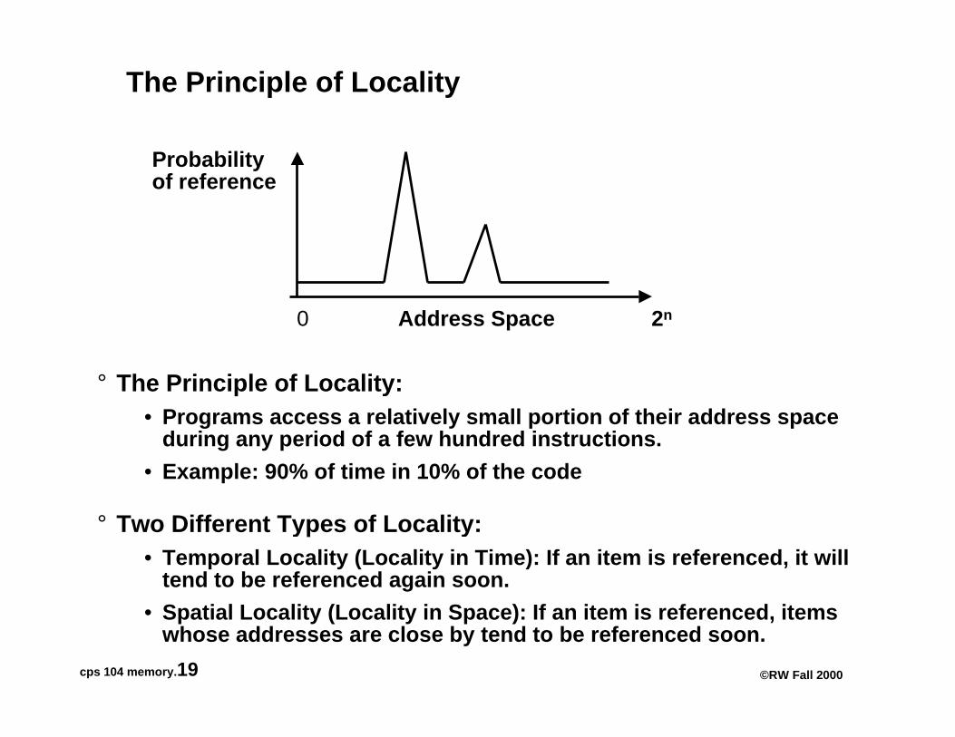
The Principle of Locality
° The Principle of Localit y:• Programs access a relatively small portion of their address space
during any period of a few hundred instructions.
• Example: 90% of time in 10% of the code
° Two Different T ypes of Localit y:• Temporal Locality (Locality in Time): If an item is referenced, it will
tend to be referenced again soon.
• Spatial Locality (Locality in Space): If an item is referenced, itemswhose addresses are close by tend to be referenced soon.
Address Space0 2n
Probabilityof reference
cps 104 memory. 20 ©RW Fall 2000
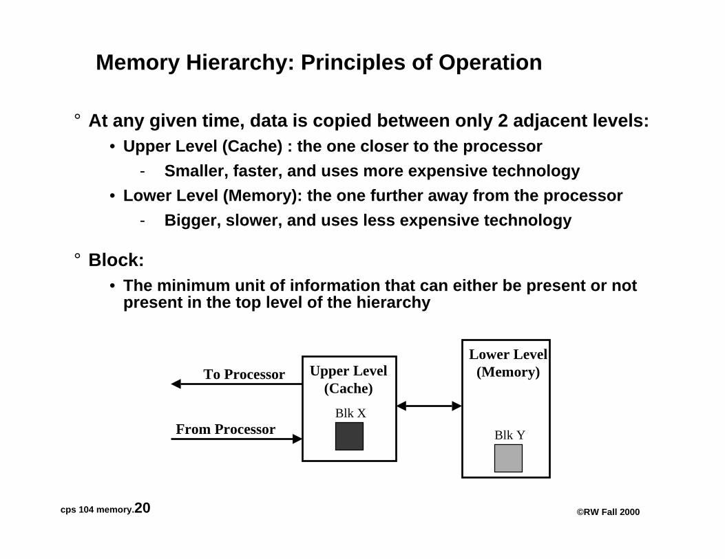
Memory Hierarchy: Principles of Operation
° At an y given time, data is copied between onl y 2 adjacent levels:• Upper Level (Cache) : the one closer to the processor
- Smaller, faster, and uses more expensive technology
• Lower Level (Memory): the one further away from the processor
- Bigger, slower, and uses less expensive technology
° Block:• The minimum unit of information that can either be present or not
present in the top level of the hierarchy
Lower Level(Memory)Upper Level
(Cache)To Processor
From ProcessorBlk X
Blk Y
cps 104 memory. 21 ©RW Fall 2000
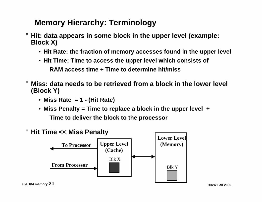
Memory Hierarchy: Terminolo gy
° Hit: data appears in some block in the upper level (example:Block X)
• Hit Rate: the fraction of memory accesses found in the upper level
• Hit Time: Time to access the upper level which consists of
RAM access time + Time to determine hit/miss
° Miss: data needs to be retrieved from a block in the lower level(Block Y)
• Miss Rate = 1 - (Hit Rate)
• Miss Penalty = Time to replace a block in the upper level +
Time to deliver the block to the processor
° Hit Time << Miss Penalt yLower Level(Memory)Upper Level
(Cache)To Processor
From ProcessorBlk X
Blk Y
cps 104 memory. 22 ©RW Fall 2000
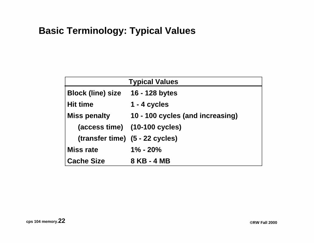
Basic Terminolo gy: Typical Values
Typical Values
Block (line) size 16 - 128 bytes
Hit time 1 - 4 cycles
Miss penalty 10 - 100 cycles (and increasing)
(access time) (10-100 cycles)
(transfer time) (5 - 22 cycles)
Miss rate 1% - 20%
Cache Size 8 KB - 4 MB
cps 104 memory. 23 ©RW Fall 2000
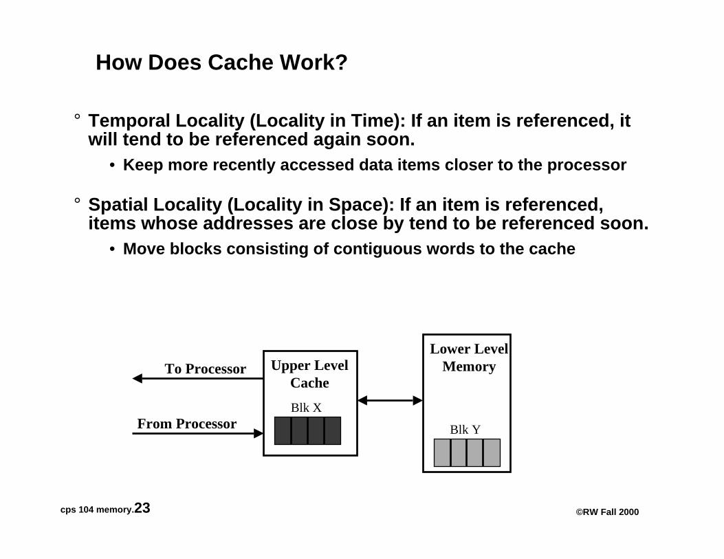
How Does Cache Work?
° Temporal Localit y (Localit y in Time): If an item is referenced, itwill tend to be referenced a gain soon.
• Keep more recently accessed data items closer to the processor
° Spatial Localit y (Localit y in Space): If an item is referenced,items whose addresses are close b y tend to be referenced soon.
• Move blocks consisting of contiguous words to the cache
Lower LevelMemoryUpper Level
CacheTo Processor
From ProcessorBlk X
Blk Y
cps 104 memory. 24 ©RW Fall 2000
Cache Implementation Principles
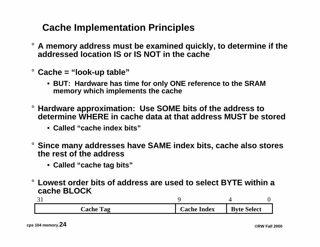
° A memor y address must be examined quickl y, to determine if theaddressed location IS or IS NOT in the cache
° Cache = “look-up table”• BUT: Hardware has time for only ONE reference to the SRAM
memory which implements the cache
° Hardware approximation: Use SOME bits of the address todetermine WHERE in cache data at that address MUST be stored
• Called “cache index bits”
° Since man y addresses have SAME index bits, cache also storesthe rest of the address
• Called “cache tag bits”
° Lowest order bits of address are used to select BYTE within acache BLOCK
Cache Index
0431
Cache Tag Byte Select
9
cps 104 memory. 25 ©RW Fall 2000
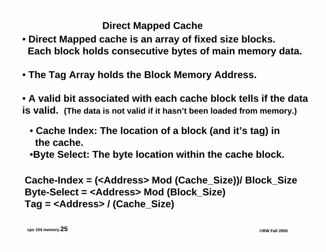
• Direct Mapped cache is an array of fixed size blocks. Each block holds consecutive bytes of main memory data.
• The Tag Array holds the Block Memory Address.
• A valid bit associated with each cache block tells if the datais valid. (The data is not valid if it hasn’t been loaded from memor y.)
Direct Mapped Cache
Cache-Index = (<Address> Mod (Cache_Size))/ Block_SizeByte-Select = <Address> Mod (Block_Size)Tag = <Address> / (Cache_Size)
• Cache Index: The location of a block (and it’s ta g) in the cache.•Byte Select: The byte location within the cache block.
cps 104 memory. 26 ©RW Fall 2000
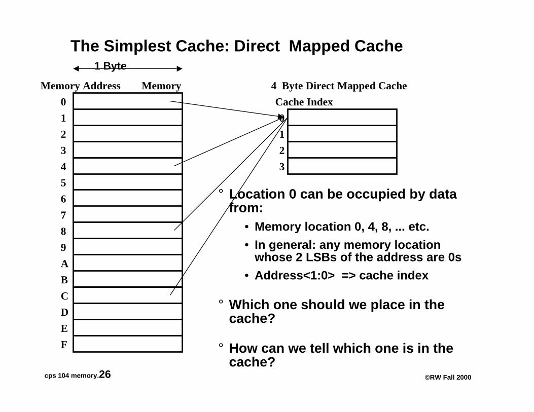
The Simplest Cache: Direct Mapped Cache
Memory 4 Byte Direct Mapped CacheMemory Address
0
1
2
3
4
5
6
7
8
9
A
B
C
D
E
F
Cache Index
0
1
2
3
° Location 0 can be occupied b y datafrom:
• Memory location 0, 4, 8, ... etc.
• In general: any memory locationwhose 2 LSBs of the address are 0s
• Address<1:0> => cache index
° Which one should we place in thecache?
° How can we tell which one is in thecache?
1 Byte
cps 104 memory. 27 ©RW Fall 2000
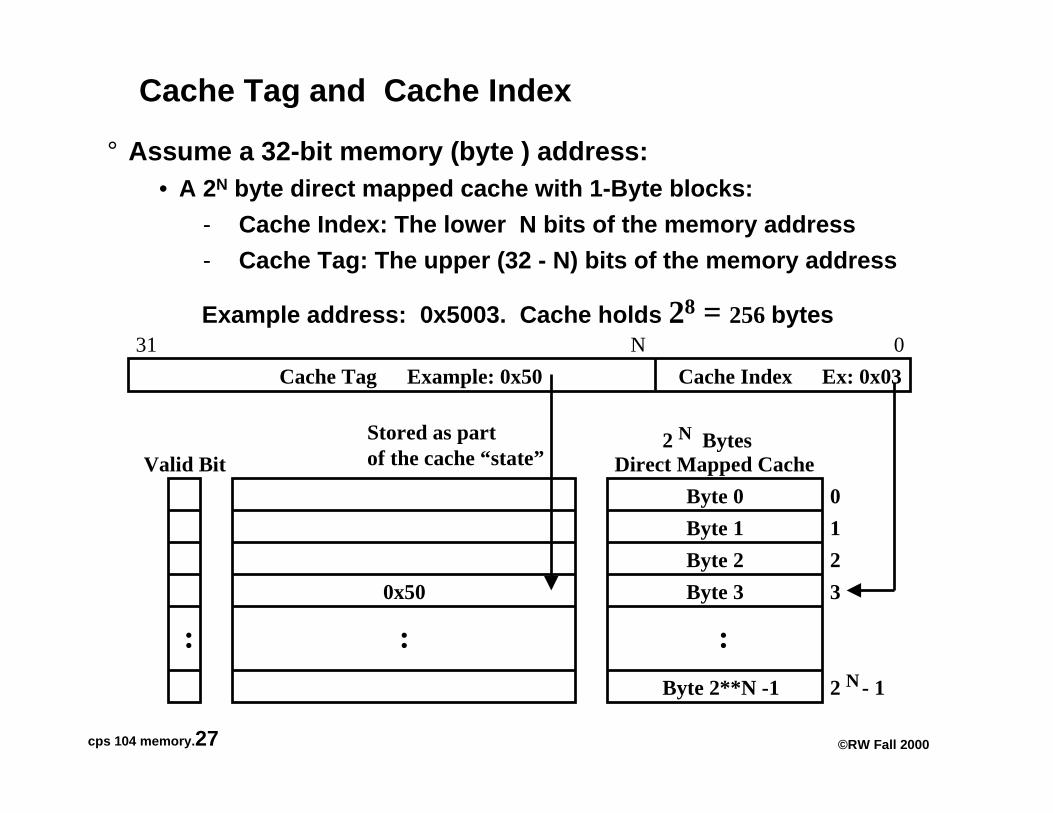
Cache Tag and Cache Index
° Assume a 32-bit memor y (byte ) address:• A 2N byte direct mapped cache with 1-Byte blocks:
- Cache Index: The lower N bits of the memory address
- Cache Tag: The upper (32 - N) bits of the memory address
Cache Index
0
1
2
3
2 - 1N
:
2 N BytesDirect Mapped Cache
Byte 0
Byte 1
Byte 2
Byte 3
Byte 2**N -1
0N31
:
Cache Tag Example: 0x50 Ex: 0x03
0x50
Stored as partof the cache “state”Valid Bit
:
Example address: 0x5003. Cache holds 28 = 256 bytes
cps 104 memory. 28 ©RW Fall 2000
Cache Access Example
Access 000 01
Start Up
000 M [00001]
Access 010 10
(miss)
(miss)
000 M [00001]
010 M [01010]
Tag DataV
000 M [00001]
010 M [01010]
Miss Handling:Load DataWrite Tag & Set V
Load Data
Write Tag & Set V
Access 000 01(HIT)
000 M [00001]
010 M [01010]Access 010 10(HIT)
° Sad Fact of Life:• A lot of misses at start up:
Compulsory Misses
- Cold start misses
- Process migration
cps 104 memory. 29 ©RW Fall 2000
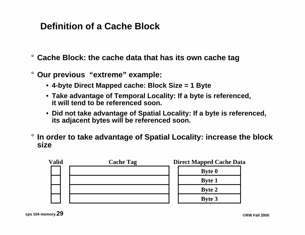
Definition of a Cache Block
° Cache Block: the cache data that has its own cache ta g
° Our previous “extreme” example:• 4-byte Direct Mapped cache: Block Size = 1 Byte
• Take advantage of Temporal Locality: If a byte is referenced,it will tend to be referenced soon.
• Did not take advantage of Spatial Locality: If a byte is referenced,its adjacent bytes will be referenced soon.
° In order to take advanta ge of Spatial Localit y: increase the blocksize
Direct Mapped Cache Data
Byte 0
Byte 1
Byte 2
Byte 3
Cache TagValid
cps 104 memory. 30 ©RW Fall 2000
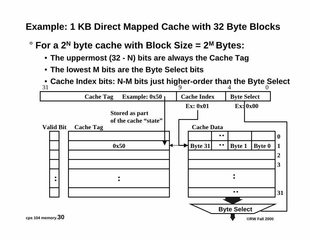
Example: 1 KB Direct Mapped Cache with 32 Byte Blocks
° For a 2N byte cache with Block Size = 2 M Bytes:• The uppermost (32 - N) bits are alwa ys the Cache Ta g
• The lowest M bits are the B yte Select bits
• Cache Index bits: N-M bits just hi gher-order than the B yte Select
Cache Index
0431
:
Cache Tag Example: 0x50
Ex: 0x01
0x50
Stored as partof the cache “state”
Valid Bit
:
0
1
2
3
:
Cache Data
31
:
Byte 0Byte 1Byte 31 :
:
Cache Tag
Byte Select
Ex: 0x00
9
Byte Select
cps 104 memory. 31 ©RW Fall 2000
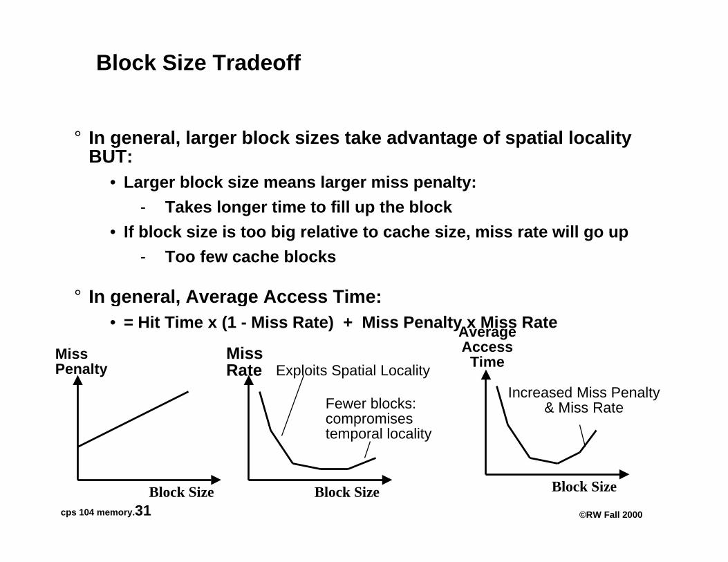
Block Size Tradeoff
° In general, lar ger block sizes take advanta ge of spatial localit yBUT:
• Larger block size means larger miss penalty:
- Takes longer time to fill up the block
• If block size is too big relative to cache size, miss rate will go up
- Too few cache blocks
° In general, Avera ge Access Time:• = Hit Time x (1 - Miss Rate) + Miss Penalty x Miss Rate
MissPenalty
Block Size
MissRate Exploits Spatial Locality
Fewer blocks: compromisestemporal locality
AverageAccess
Time
Increased Miss Penalty& Miss Rate
Block Size Block Size