Embed Size (px)
Citation preview
Rev. 0.2 10/13 Copyright © 2013 by Silicon Laboratories CP2130-EK
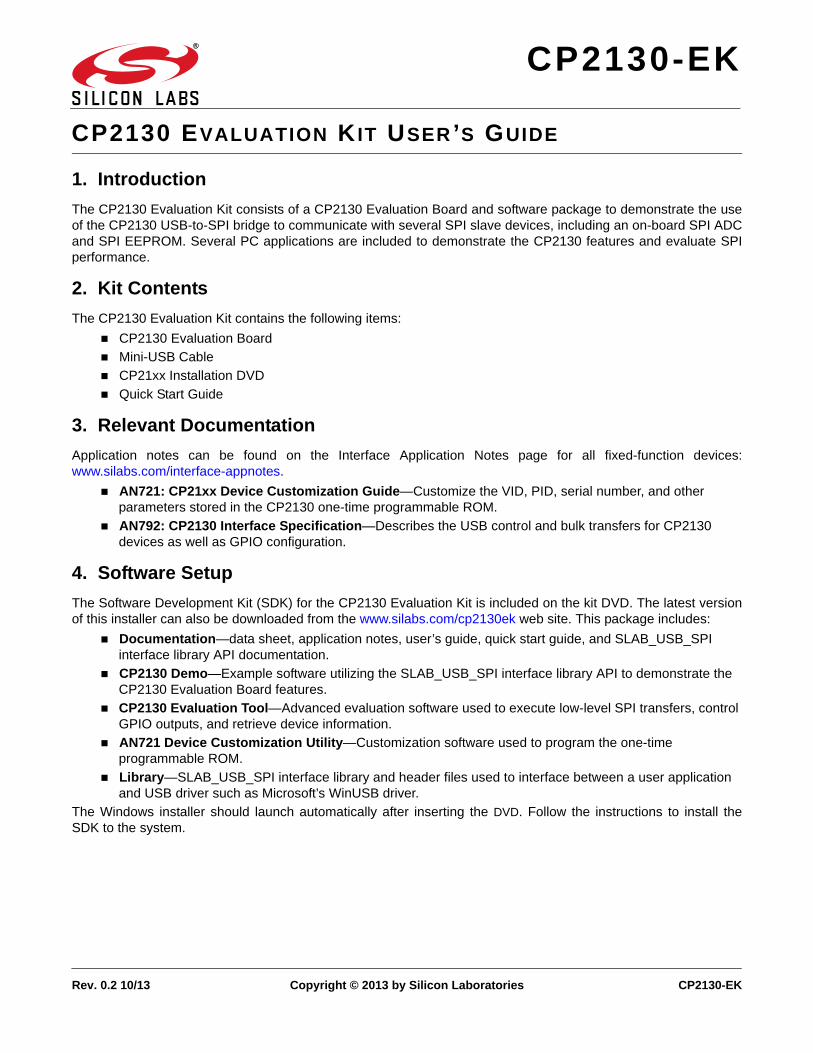
CP2130-EK
CP2130 EVALUATION KIT USER’S GUIDE
1. Introduction
The CP2130 Evaluation Kit consists of a CP2130 Evaluation Board and software package to demonstrate the useof the CP2130 USB-to-SPI bridge to communicate with several SPI slave devices, including an on-board SPI ADCand SPI EEPROM. Several PC applications are included to demonstrate the CP2130 features and evaluate SPIperformance.
2. Kit Contents
The CP2130 Evaluation Kit contains the following items:
CP2130 Evaluation Board
Mini-USB Cable
CP21xx Installation DVD
Quick Start Guide
3. Relevant Documentation
Application notes can be found on the Interface Application Notes page for all fixed-function devices:www.silabs.com/interface-appnotes.
AN721: CP21xx Device Customization Guide—Customize the VID, PID, serial number, and other parameters stored in the CP2130 one-time programmable ROM.
AN792: CP2130 Interface Specification—Describes the USB control and bulk transfers for CP2130 devices as well as GPIO configuration.
4. Software Setup
The Software Development Kit (SDK) for the CP2130 Evaluation Kit is included on the kit DVD. The latest versionof this installer can also be downloaded from the www.silabs.com/cp2130ek web site. This package includes:
Documentation—data sheet, application notes, user’s guide, quick start guide, and SLAB_USB_SPI interface library API documentation.
CP2130 Demo—Example software utilizing the SLAB_USB_SPI interface library API to demonstrate the CP2130 Evaluation Board features.
CP2130 Evaluation Tool—Advanced evaluation software used to execute low-level SPI transfers, control GPIO outputs, and retrieve device information.
AN721 Device Customization Utility—Customization software used to program the one-time programmable ROM.
Library—SLAB_USB_SPI interface library and header files used to interface between a user application and USB driver such as Microsoft’s WinUSB driver.
The Windows installer should launch automatically after inserting the DVD. Follow the instructions to install theSDK to the system.
CP2130-EK
2 Rev. 0.2
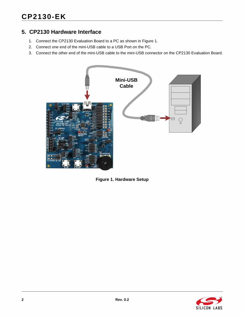
5. CP2130 Hardware Interface
1. Connect the CP2130 Evaluation Board to a PC as shown in Figure 1.
2. Connect one end of the mini-USB cable to a USB Port on the PC.
3. Connect the other end of the mini-USB cable to the mini-USB connector on the CP2130 Evaluation Board.
Figure 1. Hardware Setup
Mini-USB Cable
CP2130-EK
Rev. 0.2 3
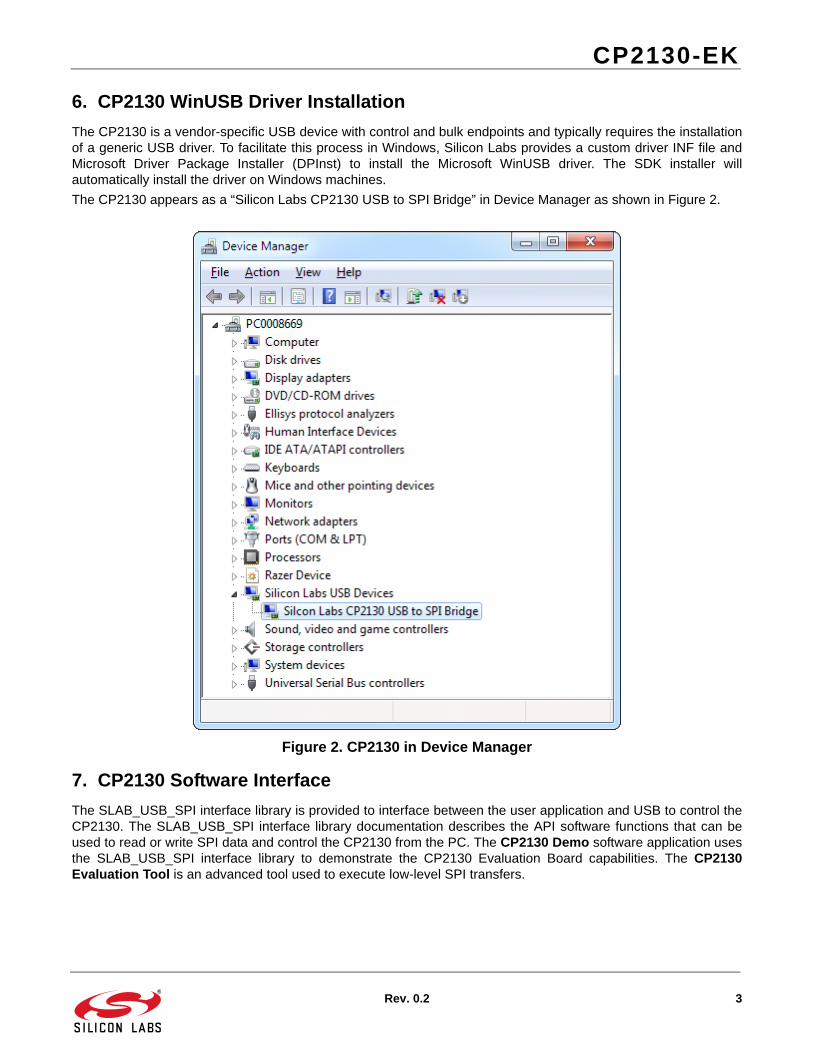
6. CP2130 WinUSB Driver Installation
The CP2130 is a vendor-specific USB device with control and bulk endpoints and typically requires the installationof a generic USB driver. To facilitate this process in Windows, Silicon Labs provides a custom driver INF file andMicrosoft Driver Package Installer (DPInst) to install the Microsoft WinUSB driver. The SDK installer willautomatically install the driver on Windows machines.
The CP2130 appears as a “Silicon Labs CP2130 USB to SPI Bridge” in Device Manager as shown in Figure 2.
Figure 2. CP2130 in Device Manager
7. CP2130 Software Interface
The SLAB_USB_SPI interface library is provided to interface between the user application and USB to control theCP2130. The SLAB_USB_SPI interface library documentation describes the API software functions that can beused to read or write SPI data and control the CP2130 from the PC. The CP2130 Demo software application usesthe SLAB_USB_SPI interface library to demonstrate the CP2130 Evaluation Board capabilities. The CP2130Evaluation Tool is an advanced tool used to execute low-level SPI transfers.
CP2130-EK
4 Rev. 0.2
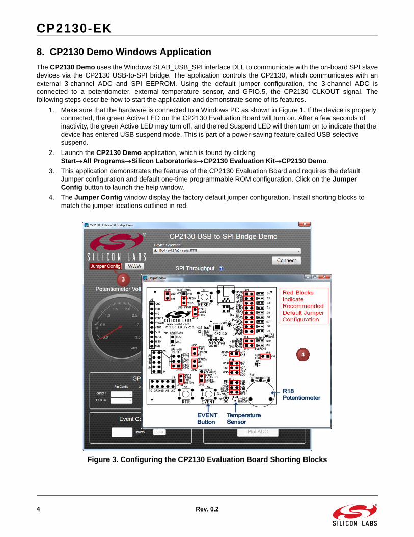
8. CP2130 Demo Windows Application
The CP2130 Demo uses the Windows SLAB_USB_SPI interface DLL to communicate with the on-board SPI slavedevices via the CP2130 USB-to-SPI bridge. The application controls the CP2130, which communicates with anexternal 3-channel ADC and SPI EEPROM. Using the default jumper configuration, the 3-channel ADC isconnected to a potentiometer, external temperature sensor, and GPIO.5, the CP2130 CLKOUT signal. Thefollowing steps describe how to start the application and demonstrate some of its features.
1. Make sure that the hardware is connected to a Windows PC as shown in Figure 1. If the device is properly connected, the green Active LED on the CP2130 Evaluation Board will turn on. After a few seconds of inactivity, the green Active LED may turn off, and the red Suspend LED will then turn on to indicate that the device has entered USB suspend mode. This is part of a power-saving feature called USB selective suspend.
2. Launch the CP2130 Demo application, which is found by clickingStartAll ProgramsSilicon LaboratoriesCP2130 Evaluation KitCP2130 Demo.
3. This application demonstrates the features of the CP2130 Evaluation Board and requires the default Jumper configuration and default one-time programmable ROM configuration. Click on the Jumper Config button to launch the help window.
4. The Jumper Config window display the factory default jumper configuration. Install shorting blocks to match the jumper locations outlined in red.
Figure 3. Configuring the CP2130 Evaluation Board Shorting Blocks
3
4
CP2130-EK
Rev. 0.2 5
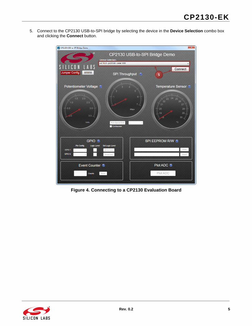
5. Connect to the CP2130 USB-to-SPI bridge by selecting the device in the Device Selection combo box and clicking the Connect button.
Figure 4. Connecting to a CP2130 Evaluation Board
5
CP2130-EK
6 Rev. 0.2
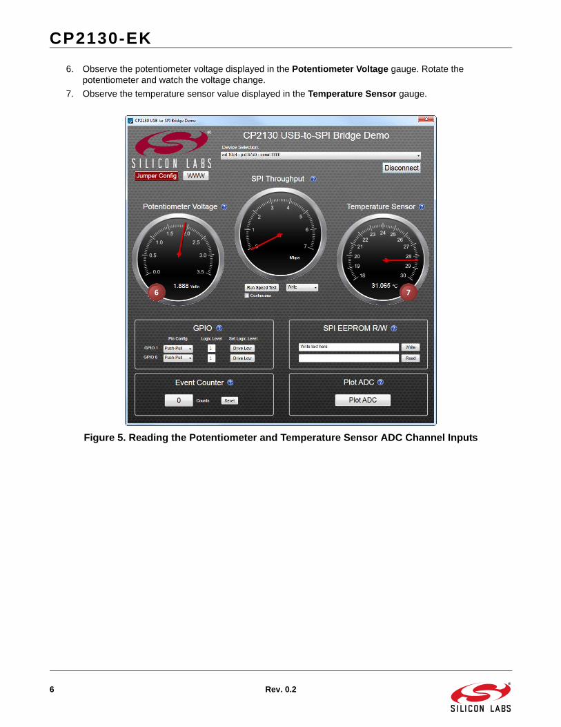
6. Observe the potentiometer voltage displayed in the Potentiometer Voltage gauge. Rotate the potentiometer and watch the voltage change.
7. Observe the temperature sensor value displayed in the Temperature Sensor gauge.
Figure 5. Reading the Potentiometer and Temperature Sensor ADC Channel Inputs
6 7
CP2130-EK
Rev. 0.2 7
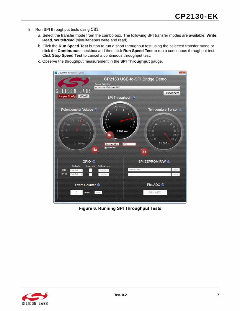
8. Run SPI throughput tests using CS1:
a. Select the transfer mode from the combo box. The following SPI transfer modes are available: Write, Read, Write/Read (simultaneous write and read).
b. Click the Run Speed Test button to run a short throughput test using the selected transfer mode or click the Continuous checkbox and then click Run Speed Test to run a continuous throughput test. Click Stop Speed Test to cancel a continuous throughput test.
c. Observe the throughput measurement in the SPI Throughput gauge.
Figure 6. Running SPI Throughput Tests
8a8b
8c
CP2130-EK
8 Rev. 0.2
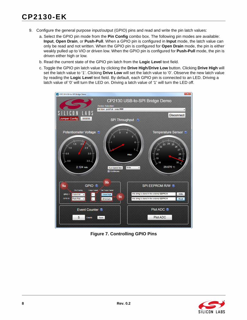
9. Configure the general purpose input/output (GPIO) pins and read and write the pin latch values:
a. Select the GPIO pin mode from the Pin Config combo box. The following pin modes are available: Input, Open Drain, or Push-Pull. When a GPIO pin is configured in Input mode, the latch value can only be read and not written. When the GPIO pin is configured for Open Drain mode, the pin is either weakly pulled up to VIO or driven low. When the GPIO pin is configured for Push-Pull mode, the pin is driven either high or low.
b. Read the current state of the GPIO pin latch from the Logic Level text field.
c. Toggle the GPIO pin latch value by clicking the Drive High/Drive Low button. Clicking Drive High will set the latch value to ‘1’. Clicking Drive Low will set the latch value to ‘0’. Observe the new latch value by reading the Logic Level text field. By default, each GPIO pin is connected to an LED. Driving a latch value of ‘0’ will turn the LED on. Driving a latch value of ‘1’ will turn the LED off.
Figure 7. Controlling GPIO Pins
9a9b
9c
CP2130-EK
Rev. 0.2 9
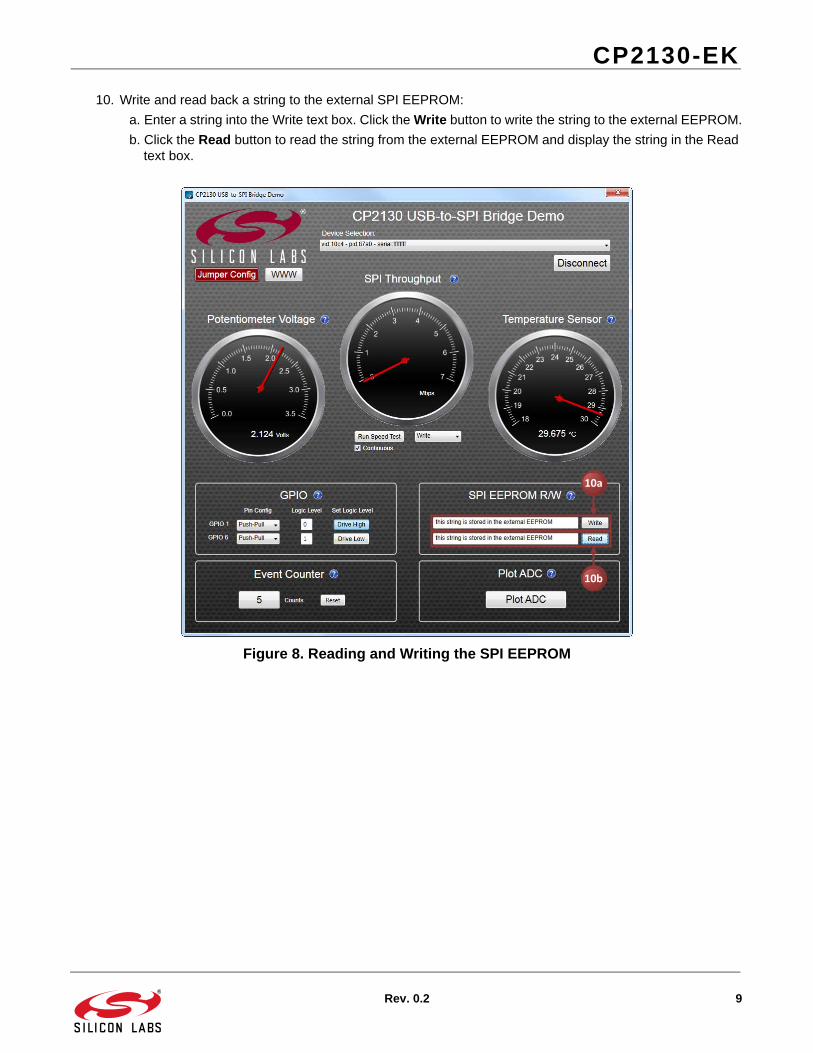
10. Write and read back a string to the external SPI EEPROM:
a. Enter a string into the Write text box. Click the Write button to write the string to the external EEPROM.
b. Click the Read button to read the string from the external EEPROM and display the string in the Read text box.
Figure 8. Reading and Writing the SPI EEPROM
10a
10b
CP2130-EK
10 Rev. 0.2
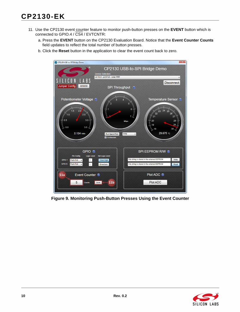
11. Use the CP2130 event counter feature to monitor push-button presses on the EVENT button which is connected to GPIO.4 / CS4 / EVTCNTR:
a. Press the EVENT button on the CP2130 Evaluation Board. Notice that the Event Counter Counts field updates to reflect the total number of button presses.
b. Click the Reset button in the application to clear the event count back to zero.
Figure 9. Monitoring Push-Button Presses Using the Event Counter
11a
11b
CP2130-EK
Rev. 0.2 11
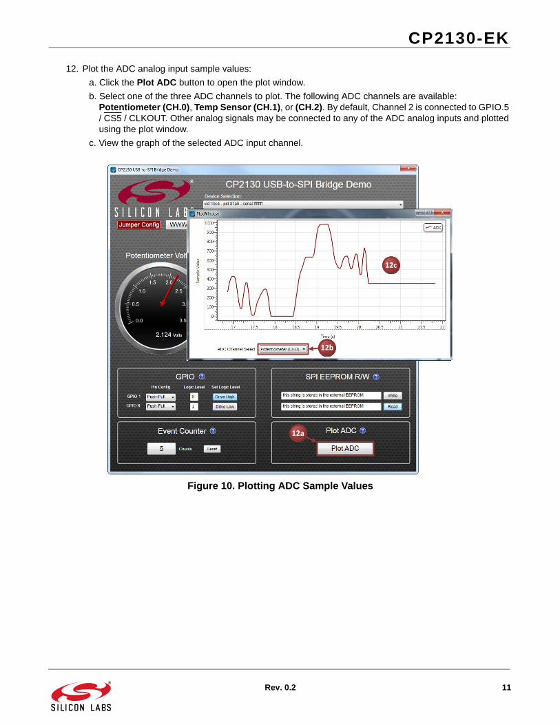
12. Plot the ADC analog input sample values:
a. Click the Plot ADC button to open the plot window.
b. Select one of the three ADC channels to plot. The following ADC channels are available: Potentiometer (CH.0), Temp Sensor (CH.1), or (CH.2). By default, Channel 2 is connected to GPIO.5 / CS5 / CLKOUT. Other analog signals may be connected to any of the ADC analog inputs and plotted using the plot window.
c. View the graph of the selected ADC input channel.
Figure 10. Plotting ADC Sample Values
12a
12b
12c
CP2130-EK
12 Rev. 0.2
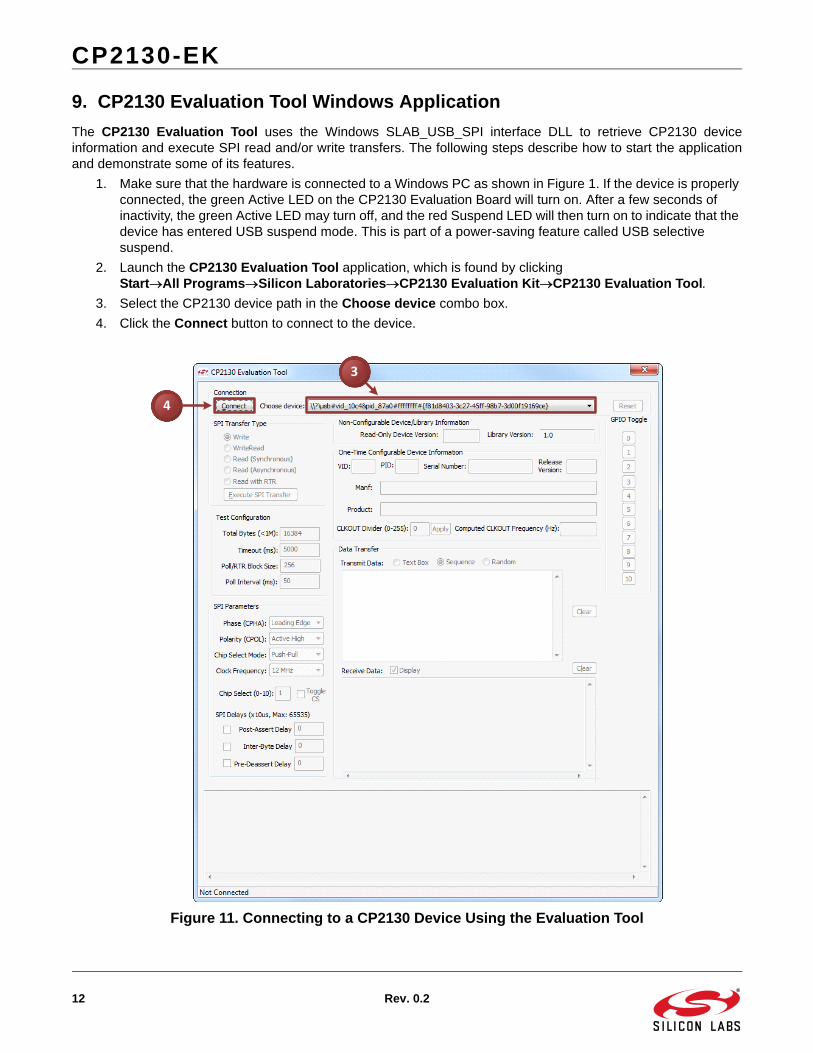
9. CP2130 Evaluation Tool Windows Application
The CP2130 Evaluation Tool uses the Windows SLAB_USB_SPI interface DLL to retrieve CP2130 deviceinformation and execute SPI read and/or write transfers. The following steps describe how to start the applicationand demonstrate some of its features.
1. Make sure that the hardware is connected to a Windows PC as shown in Figure 1. If the device is properly connected, the green Active LED on the CP2130 Evaluation Board will turn on. After a few seconds of inactivity, the green Active LED may turn off, and the red Suspend LED will then turn on to indicate that the device has entered USB suspend mode. This is part of a power-saving feature called USB selective suspend.
2. Launch the CP2130 Evaluation Tool application, which is found by clickingStartAll ProgramsSilicon LaboratoriesCP2130 Evaluation KitCP2130 Evaluation Tool.
3. Select the CP2130 device path in the Choose device combo box.
4. Click the Connect button to connect to the device.
Figure 11. Connecting to a CP2130 Device Using the Evaluation Tool
3
4
CP2130-EK
Rev. 0.2 13
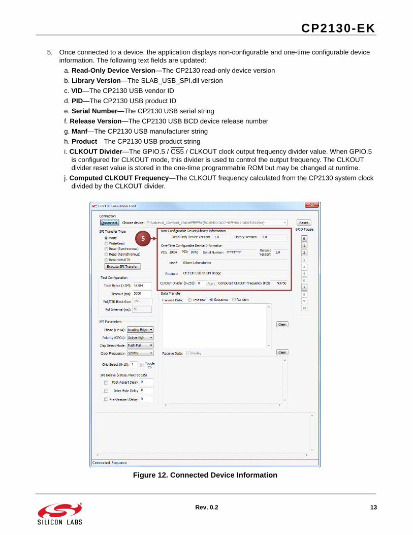
5. Once connected to a device, the application displays non-configurable and one-time configurable device information. The following text fields are updated:
a. Read-Only Device Version—The CP2130 read-only device version
b. Library Version—The SLAB_USB_SPI.dll version
c. VID—The CP2130 USB vendor ID
d. PID—The CP2130 USB product ID
e. Serial Number—The CP2130 USB serial string
f. Release Version—The CP2130 USB BCD device release number
g. Manf—The CP2130 USB manufacturer string
h. Product—The CP2130 USB product string
i. CLKOUT Divider—The GPIO.5 / CS5 / CLKOUT clock output frequency divider value. When GPIO.5 is configured for CLKOUT mode, this divider is used to control the output frequency. The CLKOUT divider reset value is stored in the one-time programmable ROM but may be changed at runtime.
j. Computed CLKOUT Frequency—The CLKOUT frequency calculated from the CP2130 system clock divided by the CLKOUT divider.
Figure 12. Connected Device Information
5
CP2130-EK
14 Rev. 0.2
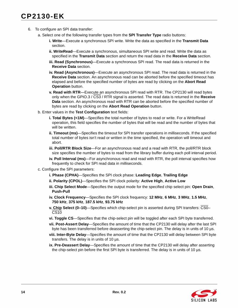
6. To configure an SPI data transfer:
a. Select one of the following transfer types from the SPI Transfer Type radio buttons:
i. Write—Execute a synchronous SPI write. Write the data as specified in the Transmit Data section.
ii. WriteRead—Execute a synchronous, simultaneous SPI write and read. Write the data as specified in the Transmit Data section and return the read data in the Receive Data section.
iii. Read (Synchronous)—Execute a synchronous SPI read. The read data is returned in the Receive Data section.
iv. Read (Asynchronous)—Execute an asynchronous SPI read. The read data is returned in the Receive Data section. An asynchronous read can be aborted before the specified timeout has elapsed and before the specified number of bytes are read by clicking on the Abort Read Operation button.
v. Read with RTR—Execute an asynchronous SPI read with RTR. The CP2130 will read bytes only when the GPIO.3 / CS3 / RTR signal is asserted. The read data is returned in the Receive Data section. An asynchronous read with RTR can be aborted before the specified number of bytes are read by clicking on the Abort Read Operation button.
b. Enter values in the Test Configuration text fields:
i. Total Bytes (<1M)—Specifies the total number of bytes to read or write. For a WriteRead operation, this field specifies the number of bytes that will be read and the number of bytes that will be written.
ii. Timeout (ms)—Specifies the timeout for SPI transfer operations in milliseconds. If the specified total number of bytes isn’t read or written in the time specified, the operation will timeout and abort.
iii. Poll/RTR Block Size—For an asynchronous read and a read with RTR, the poll/RTR block size specifies the number of bytes to read from the library buffer during each poll interval period.
iv. Poll Interval (ms)—For asynchronous read and read with RTR, the poll interval specifies how frequently to check for SPI read data in milliseconds.
c. Configure the SPI parameters:
i. Phase (CPHA)—Specifies the SPI clock phase: Leading Edge, Trailing Edge
ii. Polarity (CPOL)—Specifies the SPI clock polarity: Active High, Active Low
iii. Chip Select Mode—Specifies the output mode for the specified chip select pin: Open Drain, Push-Pull
iv. Clock Frequency—Specifies the SPI clock frequency: 12 MHz, 6 MHz, 3 MHz, 1.5 MHz, 750 kHz, 375 kHz, 187.5 kHz, 93.75 kHz
v. Chip Select (0–10)—Specifies which chip-select pin is asserted during SPI transfers: CS0–CS10
vi. Toggle CS—Specifies that the chip-select pin will be toggled after each SPI byte transferred.
vii. Post-Assert Delay—Specifies the amount of time that the CP2130 will delay after the last SPI byte has been transferred before deasserting the chip-select pin. The delay is in units of 10 µs.
viii. Inter-Byte Delay—Specifies the amount of time that the CP2130 will delay between SPI byte transfers. The delay is in units of 10 µs.
ix. Pre-Deassert Delay—Specifies the amount of time that the CP2130 will delay after asserting the chip-select pin before the first SPI byte is transferred. The delay is in units of 10 µs.
CP2130-EK
Rev. 0.2 15
Figure 13. Configuring an SPI Transfer
6a
6b
6c
CP2130-EK
16 Rev. 0.2
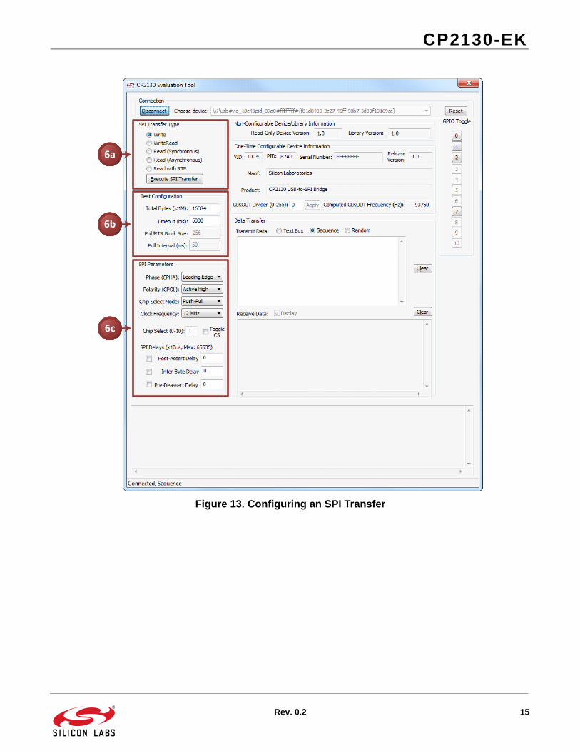
7. To execute a WriteRead SPI transfer:
a. Select the WriteRead radio button from the SPI Transfer Type group box.
b. Configure the Test Configuration and SPI Parameters, making sure to enter the number of bytes to read/write in the Total Bytes (<1M) text field.
c. Specify the data to write in the SPI transfer by selecting one of the following Transmit Data radio buttons:
i. Text Box—Enter comma-separated, hexadecimal byte values into the Transmit Data text box and send the data in the write transfer.
ii. Sequence—Write sequential data starting from 0x00 to 0xFF and repeat until the specified number of bytes are written.
iii. Random—Write random data until the specified number of bytes are written.
d. Click the Execute SPI Transfer button to start the WriteRead SPI transfer.
e. The data being read will be displayed in the Receive Data text box if the Display check box is checked.
f. The SPI transfer status and statistics will be displayed in the output text box at the bottom of the dialog.
Figure 14. Executing a WriteRead SPI Transfer
7c
7d
7e
7f
7b
7a
CP2130-EK
Rev. 0.2 17
8. To execute an asynchronous Read SPI transfer:
a. Select the Read (Asynchronous) radio button from the SPI Transfer Type group box.
b. Enter the maximum number of bytes to read in the Total Bytes (<1M) text field. Enter a maximum timeout, which specifies the maximum amount of time the read transfer can take in milliseconds. Enter the poll block size in bytes and poll interval in milliseconds.
c. Click the Execute SPI Transfer button to start the asynchronous read transfer. The button will change to Abort Read Operation while the transfer is in progress. This button can be clicked to abort the current read before the timeout elapses or the total number of bytes is read.
d. The received data will be displayed in the Receive Data text box when the application reads the poll block size every poll interval.
e. The asynchronous read transfer status will be displayed in the output text box and the status of each poll interval will be logged.
Figure 15. Executing an Asynchronous Read SPI Transfer
8a
8b
8c
8d
8e
CP2130-EK
18 Rev. 0.2
9. Click the Reset button to send the Reset command to the CP2130. After the device receives this command, it will perform a reset and re-enumerate on the bus.
10. GPIO pins configured as GPIO outputs can controlled using the GPIO Toggle buttons. Click the GPIO pin 0–10 button to toggle the output latch value. GPIO pins not configured as GPIO outputs are grayed out.
Figure 16. Resetting the Device and Toggling GPIO Pins
9
10
CP2130-EK
Rev. 0.2 19
10. CP2130 Evaluation Board Overview
The CP2130 Evaluation Kit includes an evaluation board with a CP2130 pre-installed for evaluation andpreliminary software development. The evaluation board also contains two SPI slave devices: an Si8902 IsolatedMonitoring ADC and a 256 x 8 SPI EEPROM. Figure 17 and Figure 18 highlight the CP2130 Evaluation Boardfeatures.
Figure 17. CP2130 Evaluation Board Features (Front)
LEDs
Potentiometer
ADC Headers
Temperature Sensor
Mini USB Connector
Reset Push‐Button
CP2130
Port Access
SPI Monitor
Power and SPI Test Points
CP2400 AB LCD Header
Push‐Button Switches
EEPROM Headers
CP2130-EK
20 Rev. 0.2
Figure 18. CP2130 Evaluation Board Features (Back)
EEPROM
ADC
CP2130-EK
Rev. 0.2 21
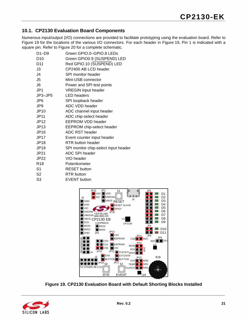
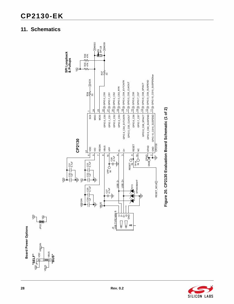
10.1. CP2130 Evaluation Board ComponentsNumerous input/output (I/O) connections are provided to facilitate prototyping using the evaluation board. Refer toFigure 19 for the locations of the various I/O connectors. For each header in Figure 19, Pin 1 is indicated with asquare pin. Refer to Figure 20 for a complete schematic.
D1–D9 Green GPIO.0–GPIO.8 LEDsD10 Green GPIO0.9 (SUSPEND) LEDD11 Red GPIO.10 (SUSPEND) LEDJ3 CP2400 AB LCD headerJ4 SPI monitor headerJ5 Mini-USB connectorJ6 Power and SPI test pointsJP1 VREGIN input headerJP3–JP5 LED headersJP6 SPI loopback headerJP9 ADC VDD headerJP10 ADC channel input headerJP11 ADC chip-select headerJP12 EEPROM VDD headerJP13 EEPROM chip-select headerJP16 ADC RST headerJP17 Event counter input headerJP18 RTR button headerJP19 SPI monitor chip-select input headerJP21 ADC SPI headerJP22 VIO headerR18 PotentiometerS1 RESET buttonS2 RTR buttonS3 EVENT button
Figure 19. CP2130 Evaluation Board with Default Shorting Blocks Installed
TO CP2400 AB LCD
VIOADC
AIN0
AIN1
AIN2
AD
C
ADC
EEPROM
VIO
CS2
EEPROM
RTR
BUTTONPOT
TEMP
CLKOUT
CLKOUT
EVTCNTR
BUTTON
CS0
VDD
VIO
MOSI
MISO
VDD
VREGIN
VBUS
RESET SLAVE
GPIO7
CP2130LOOPBACK
MOSI
SCK
MISO
CS2
CS1
CS0
D11D10
S1
S2S3
D9D8D7D6D5D4D3D2D1
RTR EVENT
U1
U4
U2
J6
SILICON LABSwww.silabs.com
JP22
JP16
JP6 JP13
JP12
JP18
JP11JP9
JP1
JP17
JP3
JP19J4
JP21
JP10
J5RESET
R18
CP2130 EB
GND
VDD
VIO
VDDSW
VREGIN
VBUS
SCK
MOSI
MISO
GND
JP4
JP5
SP
I M
ON
ITO
R
J3
CP2130-EK
22 Rev. 0.2
10.2. CP2400 AB LCD Header (J3)This header can be used to connect the CP2130 to a CP2400 AB LCD expansion board.
10.3. SPI Monitor Header (J4)The SPI monitor terminal block is included to easily interace with a SPI monitoring device with a common 10-pinribbon cable interface. See Table 1 for the SPI monitor pin definitions.
10.4. Mini-Universal Serial Bus (USB) Connector (J5)A Mini-Universal Serial Bus (USB) connector (J5) is provided to facilitate connections to the USB interface on theCP2130. See Table 2 for the USB pin definitions.
Table 1. SPI Monitor Pin Definitions
Pin # Definition
1 No Connect
2 GND
3 No Connect
4 No Connect
5 MISO
6 No Connect
7 SCK
8 MOSI
9 SPI_MON_CS (See Section 10.17)
10 GND
Table 2. Mini-USB Connector Pin Definitions
Pin # Definitions
1 VBUS
2 D-
3 D+
4 ID (No Connect)
5 GND (Ground)
CP2130-EK
Rev. 0.2 23
10.5. Power and SPI Test Points (J6)Pins 1–6 of the test point header (J6) provide easy access to the GND, VDD, VIO, VDDSW, VREGIN, and VBUSpower signals. Pins 7–10 provide easy access to the SCK, MOSI, MISO, and GND SPI signals. See Table 3 for thetest point pin definitions.
10.6. VREGIN Input Header (JP1)The CP2130 can be configured to operate in one of two power modes:
USB self-powered mode (Short Pins 1–2 on JP1)—VREGIN is shorted to VDD, the CP2130 internal voltage regulator is disabled, and an external supply voltage must be connected to the VDD test point. Do not exceed the maximum VDD voltage specification!
USB bus-powered mode (Short Pins 2–3 on JP1)—VREGIN is shorted to VBUS and the CP2130 internal voltage regulator is enabled. The board VDD is powered by the CP2130 internal voltage regulator output.
See Table 4 for the VREGIN input header pin definitions.
Table 3. Power and SPI Pin Definitions
Type Pin # Definition
Power
1 GND
2 VDD
3 VIO
4 VDDSW (Switched Supply)
5 VREGIN
6 VBUS
SPI
7 SCK
8 MOSI
9 MISO
10 GND
Table 4. VREGIN Input Header Pin Definitions
Pin # Definitions
1 VDD (Self-Powered)
2 VREGIN
3 VBUS (Bus-Powered)
CP2130-EK
24 Rev. 0.2
10.7. LED Headers (JP3, JP4, and JP5)Headers JP3, JP4, and JP5 are provided to allow access to the GPIO pins on the CP2130. Place shorting blockson JP3, JP4, and JP5 to connect the GPIO pins to the ten green LEDs, D1–D10, and the one red LED, D11. TheseLEDs can be used to indicate active communications through the CP2130. Table 5 lists the LED corresponding toeach header position.
10.8. SPI Loopback Header (JP6)To short the SPI MOSI and MISO signals, install a shorting block on JP6. This shorting block should be removedduring normal SPI operation. See Table 6 for the SPI loopback header pin definitions.
10.9. ADC VDD Header (JP9)This header provides access to the ADC VDD pin. Install a shorting block on JP9 to provide power to the ADC fromVIO. See Table 7 for the ADC VDD header pin definitions.
Table 5. JP3, JP4, and JP5 LED Header Locations
GPIO Pin LED Pins
GPIO.0 / CS0 D1 JP3[1:2]
GPIO.1 / CS1 D2 JP3[3:4]
GPIO.2 / CS2 D3 JP3[5:6]
GPIO.3 / CS3 / RTR D4 JP3[7:8]
GPIO.4 / CS4 / EVTCNTR D5 JP3[9:10]
GPIO.5 / CS5 / CLKOUT D6 JP3[11:12]
GPIO.6 / CS6 D7 JP3[13:14]
GPIO.7 / CS7 D8 JP3[15:16]
GPIO.8 / CS8 / SPIACT D9 JP3[17:18]
GPIO.9 / CS9 / SUSPEND D10 JP4[1:2]
GPIO.10 / CS10 / SUSPEND D11 JP5[1:2]
Table 6. SPI Loopback Header Pin Definitions
Pin # Definitions
1 MISO
2 MOSI
Table 7. ADC VDD Header Pin Definitions
Pin # Definitions
1 VIO
2 ADC VDD
CP2130-EK
Rev. 0.2 25
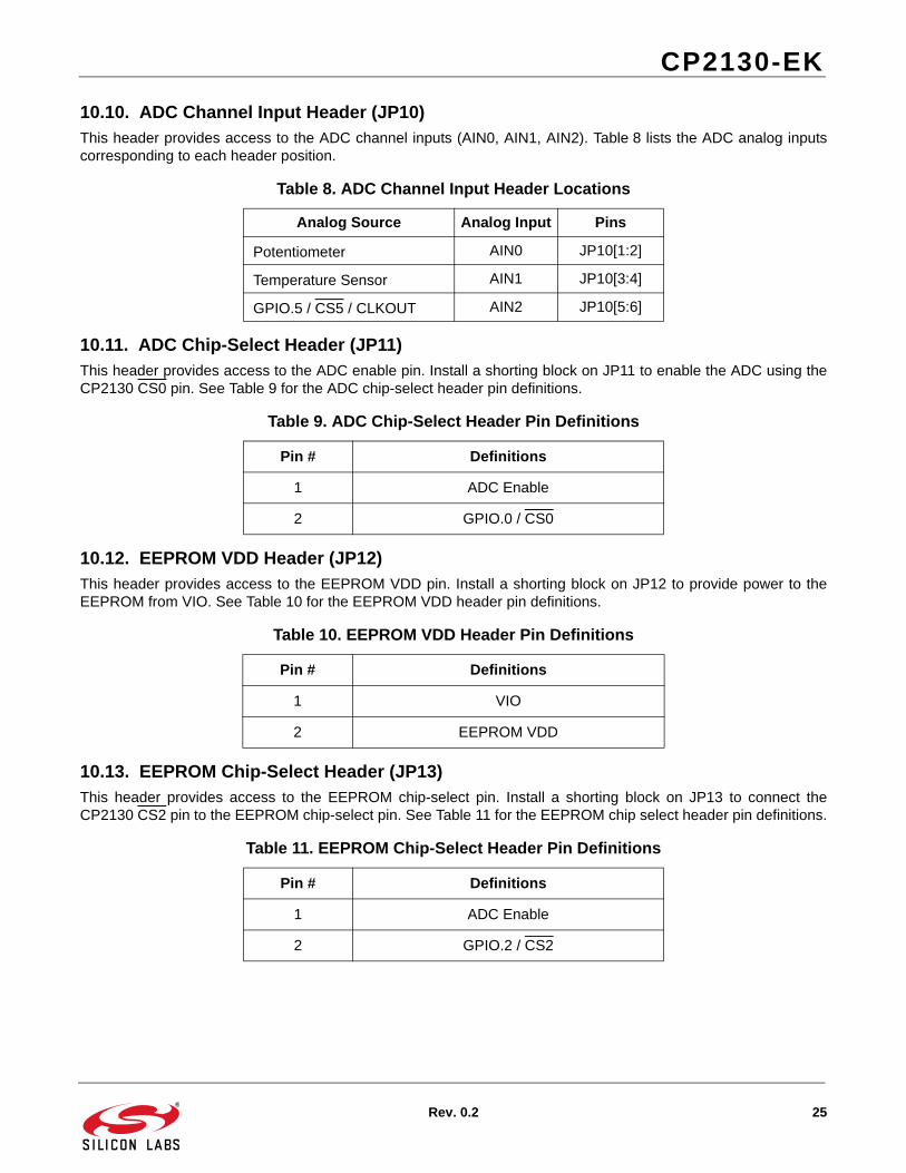
10.10. ADC Channel Input Header (JP10)This header provides access to the ADC channel inputs (AIN0, AIN1, AIN2). Table 8 lists the ADC analog inputscorresponding to each header position.
10.11. ADC Chip-Select Header (JP11)This header provides access to the ADC enable pin. Install a shorting block on JP11 to enable the ADC using theCP2130 CS0 pin. See Table 9 for the ADC chip-select header pin definitions.
10.12. EEPROM VDD Header (JP12)This header provides access to the EEPROM VDD pin. Install a shorting block on JP12 to provide power to theEEPROM from VIO. See Table 10 for the EEPROM VDD header pin definitions.
10.13. EEPROM Chip-Select Header (JP13)This header provides access to the EEPROM chip-select pin. Install a shorting block on JP13 to connect theCP2130 CS2 pin to the EEPROM chip-select pin. See Table 11 for the EEPROM chip select header pin definitions.
Table 8. ADC Channel Input Header Locations
Analog Source Analog Input Pins
Potentiometer AIN0 JP10[1:2]
Temperature Sensor AIN1 JP10[3:4]
GPIO.5 / CS5 / CLKOUT AIN2 JP10[5:6]
Table 9. ADC Chip-Select Header Pin Definitions
Pin # Definitions
1 ADC Enable
2 GPIO.0 / CS0
Table 10. EEPROM VDD Header Pin Definitions
Pin # Definitions
1 VIO
2 EEPROM VDD
Table 11. EEPROM Chip-Select Header Pin Definitions
Pin # Definitions
1 ADC Enable
2 GPIO.2 / CS2
CP2130-EK
26 Rev. 0.2
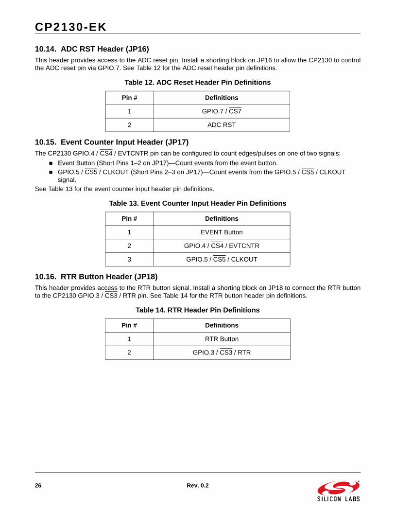
10.14. ADC RST Header (JP16)This header provides access to the ADC reset pin. Install a shorting block on JP16 to allow the CP2130 to controlthe ADC reset pin via GPIO.7. See Table 12 for the ADC reset header pin definitions.
10.15. Event Counter Input Header (JP17)The CP2130 GPIO.4 / CS4 / EVTCNTR pin can be configured to count edges/pulses on one of two signals:
Event Button (Short Pins 1–2 on JP17)—Count events from the event button.
GPIO.5 / CS5 / CLKOUT (Short Pins 2–3 on JP17)—Count events from the GPIO.5 / CS5 / CLKOUT signal.
See Table 13 for the event counter input header pin definitions.
10.16. RTR Button Header (JP18)This header provides access to the RTR button signal. Install a shorting block on JP18 to connect the RTR buttonto the CP2130 GPIO.3 / CS3 / RTR pin. See Table 14 for the RTR button header pin definitions.
Table 12. ADC Reset Header Pin Definitions
Pin # Definitions
1 GPIO.7 / CS7
2 ADC RST
Table 13. Event Counter Input Header Pin Definitions
Pin # Definitions
1 EVENT Button
2 GPIO.4 / CS4 / EVTCNTR
3 GPIO.5 / CS5 / CLKOUT
Table 14. RTR Header Pin Definitions
Pin # Definitions
1 RTR Button
2 GPIO.3 / CS3 / RTR
CP2130-EK
Rev. 0.2 27
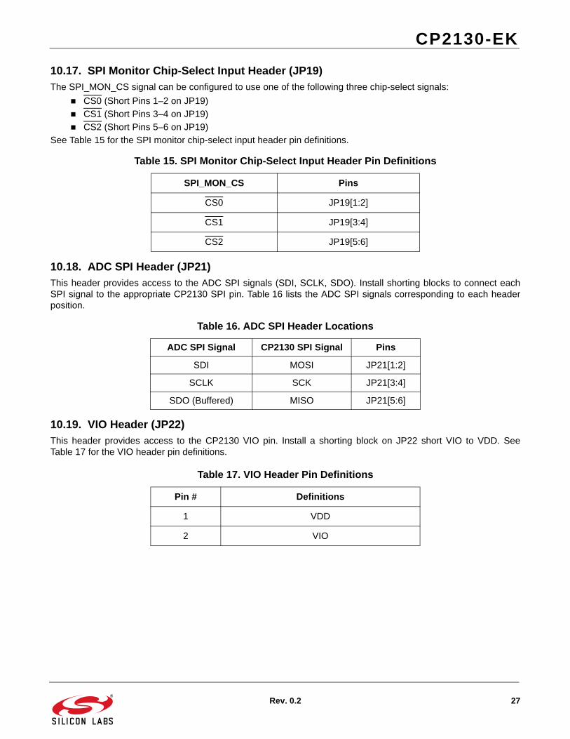
10.17. SPI Monitor Chip-Select Input Header (JP19)The SPI_MON_CS signal can be configured to use one of the following three chip-select signals:
CS0 (Short Pins 1–2 on JP19)
CS1 (Short Pins 3–4 on JP19)
CS2 (Short Pins 5–6 on JP19)
See Table 15 for the SPI monitor chip-select input header pin definitions.
10.18. ADC SPI Header (JP21)This header provides access to the ADC SPI signals (SDI, SCLK, SDO). Install shorting blocks to connect eachSPI signal to the appropriate CP2130 SPI pin. Table 16 lists the ADC SPI signals corresponding to each headerposition.
10.19. VIO Header (JP22)This header provides access to the CP2130 VIO pin. Install a shorting block on JP22 short VIO to VDD. SeeTable 17 for the VIO header pin definitions.
Table 15. SPI Monitor Chip-Select Input Header Pin Definitions
SPI_MON_CS Pins
CS0 JP19[1:2]
CS1 JP19[3:4]
CS2 JP19[5:6]
Table 16. ADC SPI Header Locations
ADC SPI Signal CP2130 SPI Signal Pins
SDI MOSI JP21[1:2]
SCLK SCK JP21[3:4]
SDO (Buffered) MISO JP21[5:6]
Table 17. VIO Header Pin Definitions
Pin # Definitions
1 VDD
2 VIO
CP2130-EK
28 Rev. 0.2
11. Schematics
US
B_D
-
US
B_D
+
VB
US
VD
D
VIO
VD
D
VIO
VB
US
VR
EG
IN
VB
US
VR
EG
INV
IO
VD
DV
DD
SC
K
MO
SI
RE
SE
T_M
CU
MIS
O
GP
IO.0
_CS
0
GP
IO.2
_CS
2
GP
IO.4
_CS
4_E
VTC
NTR
GP
IO.6
_CS
6
GP
IO.8
_CS
8_S
PIA
CT
GP
IO.1
0_C
S10
_SU
SP
EN
Dba
r
GP
IO.1
_CS
1
GP
IO.3
_CS
3_R
TR
GP
IO.7
_CS
7
GP
IO.9
_CS
9_S
US
PE
ND
GP
IO.5
_CS
5_C
LKO
UT
CP2
130
SPI L
oopb
ack
& P
ullu
ps
"SEL
F"
"BU
S"Boa
rd P
ower
Opt
ions
C24
1uF
J5 US
B T
YP
E M
INI B
+V D-
D+ ID
GN
D
SHSH
C27
4.7u
F D13
SP
0503
BA
HT
JP22
R34
33
C26
4.7u
F
JP1
TP18
NI
R37
33
C23
0.1u
FC
221u
F
R35
47K
RE
SE
T NI
GN
D
R36
47K
U1 CP
2130
VD
D6
VIO
5
RE
GIN
7
GN
D2
RE
SE
T9
GP
IO.5
_CS
5_C
LKO
UT
17
VB
US
8
D+
3D
-4
GP
IO.4
_CS
4_E
VTC
NTR
18G
PIO
.3_C
S3
19
GP
IO.0
_CS
022
GP
IO.2
_CS
220
MO
SI
23
GP
IO.1
_CS
121
MIS
O24
SC
K1
GP
IO.1
0_C
S10
_SU
SP
EN
D11
GP
IO.9
_CS
9_S
US
PE
ND
12G
PIO
.8_C
S8_
SP
IAC
T13
GP
IO.7
_CS
714
EP
AD
EP
AD
NC
10
VP
P16
GP
IO.6
_CS
615
JP6
SP
I LB
C21
0.1u
F
VP
PN
I
C20
1uF
C25
0.1u
F
Fig
ure
20.
CP
213
0 E
val
ua
tio
n B
oar
d S
ch
ema
tic
(1
of
2)
CP2130-EK
Rev. 0.2 29
EE
PR
OM
_VD
D
AD
C_V
DD
SP
I_M
ON
_CS
CS
0C
S1
CS
2
CLK
_OU
T
EV
EN
T B
UTT
ON
VIO
VIO
VIO
VIO
VIO
VIO
VIO
VIO
VD
DV
IO
VR
EG
INV
BU
S
VD
DS
W
VD
DV
DD
SW
SC
K
MIS
O
MO
SI
RE
SE
T_M
CU
MIS
O
GP
IO.7
_CS
7
GP
IO.4
_CS
4_E
VTC
NTR
GP
IO.5
_CS
5_C
LKO
UT
GP
IO.3
_CS
3_R
TR
GP
IO.1
_CS
1
GP
IO.5
_CS
5_C
LKO
UT
GP
IO.6
_CS
6
GP
IO.2
_CS
2
GP
IO.5
_CS
5_C
LKO
UT
GP
IO.0
_CS
0
GP
IO.0
_CS
0G
PIO
.1_C
S1
GP
IO.2
_CS
2
GP
IO.0
_CS
0
GP
IO.2
_CS
2
GP
IO.4
_CS
4_E
VTC
NTR
GP
IO.6
_CS
6
GP
IO.8
_CS
8_S
PIA
CT
GP
IO.1
0_C
S10
_SU
SP
EN
Dba
r
GP
IO.1
_CS
1
GP
IO.3
_CS
3_R
TR
GP
IO.5
_CS
5_C
LKO
UT
GP
IO.7
_CS
7
GP
IO.9
_CS
9_S
US
PE
ND
RE
SE
T_S
LAV
ER
ES
ET_
SLA
VE
MIS
OS
CK
RE
SE
T_S
LAV
E
MO
SI
SC
KM
OS
I
SC
K
MIS
OM
OS
I
SC
K
MIS
O
MO
SI
GP
IO.9
_CS
9_S
US
PE
ND
Buf
fer E
nabl
e (a
ctiv
e lo
w)
RTR
(Rea
dy T
o R
ead)
Pus
hbut
ton
Test
Poi
nts
Even
t Pus
hbut
ton
Res
et C
ircui
try
CP2
130
GPI
O a
nd M
ulti-
purp
ose
Line
sSi
8902
Isol
ated
Mon
itorin
g A
DC
(CS0
)
256x
8 SP
I EEP
RO
M (C
S2)
Con
nect
ion
to E
xter
nal S
PI/I2
C M
onito
r
Con
nect
ion
to C
P240
0 A
B L
CD
Con
trol
ler E
VB (C
S1)
INT
CLK
NS
S
RS
T
Switc
hed
VIO
Sup
ply
R6
470
C7
1uF
U3
25A
A02
E48
/CS
1M
ISO
2M
OS
I5
SC
LK6
/WP
3
GND4
/HO
LD7
VCC8
D5
GP
IO4
R30
0
R14
470
JP18
RTR
JP11
C1
1uF
C28
1uF
NI
R5
470
J4
SP
I MO
NIT
OR
1 3 5
2 4 67
89
10
R12
1K
C14
0.1u
F
D3
GP
IO2
JP13
R3
470
R39
0
R13
1K
R10
470
D11
RE
D
SU
SP
EN
D
R23
1K
R41
0
R28
0R
1147
0
U4
MC
P97
01A
T
GN
D
3
VD
D1
VO
UT
2
M1
NTR
4171
PT1
GG
NDD
4G
PIO
3R
447
0
S1
RE
SE
T
JP4
R32
33
R18
10K
13
2
C5 1u
F
S2
EV
EN
T
C19
0.1u
F
JP9
D2
GP
IO1
D10
AC
TIV
E
R2
470
D7
GP
IO6
C2
0.1u
F
R27
0
GN
D
R20
1K
JP10 1 3
2 45
6
D1
GP
IO0
C6
0.1u
F R26
0
S3
RTR
R7
470
JP19
SP
I MO
NIT
OR
CS
SE
L
1 32 4
56
JP3
1 3 5
2 4 67
89
1011
1213
1415
1617
18
C4
0.1u
F
C29
0.1u
F
R1
470
U5
Si8
902
VD
DA
1
RS
T2
VR
EF
4
AIN
27
AIN
05
VD
DB
10
GN
DA
8G
ND
B9
SD
I12
EN
11
NC
3
AIN
16
SC
LK13
SD
O14
NC
15V
DD
B16
D12
BA
T54C
R25
0
HE
AD
ER
0.1
in-1
x10
J6
1091 53 62 4 87
R31
2.05
K
U2
74A
UP
1G12
52
4
5 31
C30 1u
F
C10
0.1u
F
D8
GP
IO7
R22
10K
JP12
R21
10K
R8
470
JP16
C9
1uF
D9
GP
IO8
JP17
R29
0
J3
CP
2400
EV
B
NI
1 3 5
2 4 67
89
10
R9
470
R42
200
JP21
1324
56
C8
0.1u
F
R40
0
JP5
D6
GP
IO5
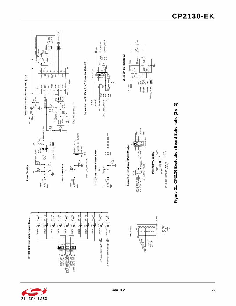
Fig
ure
21.
CP
213
0 E
valu
ati
on
Bo
ard
Sc
hem
ati
c (2
of
2)
CP2130-EK
30 Rev. 0.2
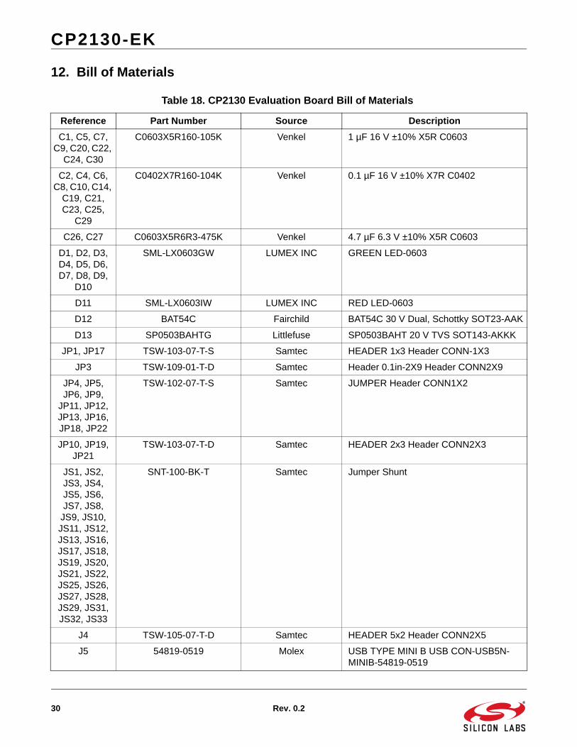
12. Bill of Materials
Table 18. CP2130 Evaluation Board Bill of Materials
Reference Part Number Source Description
C1, C5, C7, C9, C20, C22,
C24, C30
C0603X5R160-105K Venkel 1 µF 16 V ±10% X5R C0603
C2, C4, C6, C8, C10, C14,
C19, C21, C23, C25,
C29
C0402X7R160-104K Venkel 0.1 µF 16 V ±10% X7R C0402
C26, C27 C0603X5R6R3-475K Venkel 4.7 µF 6.3 V ±10% X5R C0603
D1, D2, D3, D4, D5, D6, D7, D8, D9,
D10
SML-LX0603GW LUMEX INC GREEN LED-0603
D11 SML-LX0603IW LUMEX INC RED LED-0603
D12 BAT54C Fairchild BAT54C 30 V Dual, Schottky SOT23-AAK
D13 SP0503BAHTG Littlefuse SP0503BAHT 20 V TVS SOT143-AKKK
JP1, JP17 TSW-103-07-T-S Samtec HEADER 1x3 Header CONN-1X3
JP3 TSW-109-01-T-D Samtec Header 0.1in-2X9 Header CONN2X9
JP4, JP5, JP6, JP9,
JP11, JP12, JP13, JP16, JP18, JP22
TSW-102-07-T-S Samtec JUMPER Header CONN1X2
JP10, JP19, JP21
TSW-103-07-T-D Samtec HEADER 2x3 Header CONN2X3
JS1, JS2, JS3, JS4, JS5, JS6, JS7, JS8,
JS9, JS10, JS11, JS12, JS13, JS16, JS17, JS18, JS19, JS20, JS21, JS22, JS25, JS26, JS27, JS28, JS29, JS31, JS32, JS33
SNT-100-BK-T Samtec Jumper Shunt
J4 TSW-105-07-T-D Samtec HEADER 5x2 Header CONN2X5
J5 54819-0519 Molex USB TYPE MINI B USB CON-USB5N-MINIB-54819-0519
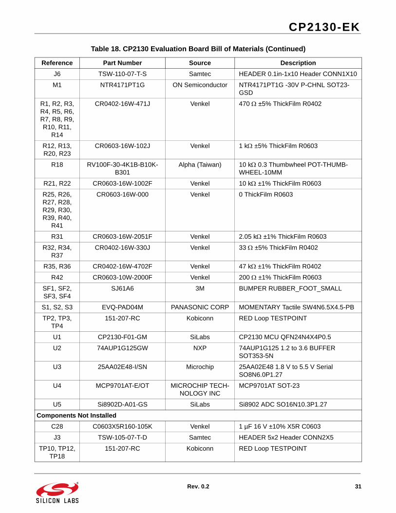
CP2130-EK
Rev. 0.2 31
J6 TSW-110-07-T-S Samtec HEADER 0.1in-1x10 Header CONN1X10
M1 NTR4171PT1G ON Semiconductor NTR4171PT1G -30V P-CHNL SOT23-GSD
R1, R2, R3, R4, R5, R6, R7, R8, R9, R10, R11,
R14
CR0402-16W-471J Venkel 470 ±5% ThickFilm R0402
R12, R13, R20, R23
CR0603-16W-102J Venkel 1 k ±5% ThickFilm R0603
R18 RV100F-30-4K1B-B10K-B301
Alpha (Taiwan) 10 k 0.3 Thumbwheel POT-THUMB-WHEEL-10MM
R21, R22 CR0603-16W-1002F Venkel 10 k ±1% ThickFilm R0603
R25, R26, R27, R28, R29, R30, R39, R40,
R41
CR0603-16W-000 Venkel 0 ThickFilm R0603
R31 CR0603-16W-2051F Venkel 2.05 k ±1% ThickFilm R0603
R32, R34, R37
CR0402-16W-330J Venkel 33 ±5% ThickFilm R0402
R35, R36 CR0402-16W-4702F Venkel 47 k ±1% ThickFilm R0402
R42 CR0603-10W-2000F Venkel 200 ±1% ThickFilm R0603
SF1, SF2, SF3, SF4
SJ61A6 3M BUMPER RUBBER_FOOT_SMALL
S1, S2, S3 EVQ-PAD04M PANASONIC CORP MOMENTARY Tactile SW4N6.5X4.5-PB
TP2, TP3, TP4
151-207-RC Kobiconn RED Loop TESTPOINT
U1 CP2130-F01-GM SiLabs CP2130 MCU QFN24N4X4P0.5
U2 74AUP1G125GW NXP 74AUP1G125 1.2 to 3.6 BUFFER SOT353-5N
U3 25AA02E48-I/SN Microchip 25AA02E48 1.8 V to 5.5 V Serial SO8N6.0P1.27
U4 MCP9701AT-E/OT MICROCHIP TECH-NOLOGY INC
MCP9701AT SOT-23
U5 Si8902D-A01-GS SiLabs Si8902 ADC SO16N10.3P1.27
Components Not Installed
C28 C0603X5R160-105K Venkel 1 µF 16 V ±10% X5R C0603
J3 TSW-105-07-T-D Samtec HEADER 5x2 Header CONN2X5
TP10, TP12, TP18
151-207-RC Kobiconn RED Loop TESTPOINT
Table 18. CP2130 Evaluation Board Bill of Materials (Continued)
Reference Part Number Source Description

http://www.silabs.com
Silicon Laboratories Inc.400 West Cesar ChavezAustin, TX 78701USA
Simplicity Studio
One-click access to MCU and wireless tools, documentation, software, source code libraries & more. Available for Windows, Mac and Linux!
IoT Portfoliowww.silabs.com/IoT
SW/HWwww.silabs.com/simplicity
Qualitywww.silabs.com/quality
Support and Communitycommunity.silabs.com
DisclaimerSilicon Labs intends to provide customers with the latest, accurate, and in-depth documentation of all peripherals and modules available for system and software implementers using or intending to use the Silicon Labs products. Characterization data, available modules and peripherals, memory sizes and memory addresses refer to each specific device, and "Typical" parameters provided can and do vary in different applications. Application examples described herein are for illustrative purposes only. Silicon Labs reserves the right to make changes without further notice and limitation to product information, specifications, and descriptions herein, and does not give warranties as to the accuracy or completeness of the included information. Silicon Labs shall have no liability for the consequences of use of the information supplied herein. This document does not imply or express copyright licenses granted hereunder to design or fabricate any integrated circuits. The products are not designed or authorized to be used within any Life Support System without the specific written consent of Silicon Labs. A "Life Support System" is any product or system intended to support or sustain life and/or health, which, if it fails, can be reasonably expected to result in significant personal injury or death. Silicon Labs products are not designed or authorized for military applications. Silicon Labs products shall under no circumstances be used in weapons of mass destruction including (but not limited to) nuclear, biological or chemical weapons, or missiles capable of delivering such weapons.
Trademark InformationSilicon Laboratories Inc.® , Silicon Laboratories®, Silicon Labs®, SiLabs® and the Silicon Labs logo®, Bluegiga®, Bluegiga Logo®, Clockbuilder®, CMEMS®, DSPLL®, EFM®, EFM32®, EFR, Ember®, Energy Micro, Energy Micro logo and combinations thereof, "the world’s most energy friendly microcontrollers", Ember®, EZLink®, EZRadio®, EZRadioPRO®, Gecko®, ISOmodem®, Precision32®, ProSLIC®, Simplicity Studio®, SiPHY®, Telegesis, the Telegesis Logo®, USBXpress® and others are trademarks or registered trademarks of Silicon Labs. ARM, CORTEX, Cortex-M3 and THUMB are trademarks or registered trademarks of ARM Holdings. Keil is a registered trademark of ARM Limited. All other products or brand names mentioned herein are trademarks of their respective holders.