Embed Size (px)
Citation preview

Course Handout S6 EEE
2017
Rajagiri School of Engineering and Technology
1/1/2017

Rajagiri School of Engineering & Technology Page 2
RSET Vision
• To evolve into a premier technological and research institution,moulding eminent professionals with creative minds, innovativeideas and sound practical skill, and to shape a future wheretechnology works for the enrichment of mankind.
RSET Mission
• To impart state-of-the-art knowledge to individuals in varioustechnological disciplines and to inculcate in them a high degreeof social consciousness and human values, thereby enablingthem to face the challenges of life with courage and conviction

Rajagiri School of Engineering & Technology Page 3
Department Vision
• To excel in Electrical and Electronics Engineering education withfocus on research to make professionals with creative minds,innovative ideas and practical skills for the betterment ofmankind.
Department Mission
• To develop and disseminate among the individuals, thetheoretical foundation, practical aspects in the field of Electricaland Electronics Engineering and inculcate a high degree ofprofessional and social ethics for creating successful engineers.

Rajagiri School of Engineering & Technology Page 4
PROGRAMME EDUCATIONAL OBJECTIVES
PEO 1
• To provide Graduates with a solid foundation in mathematical, scientificand engineering fundamentals and depth and breadth studies inElectrical and Electronics engineering, so as to comprehend, analyse,design, provide solutions for practical issues in engineering.
PEO 2• To strive for Graduates achievement and success in the profession or
higher studies, which they may pursue.
PEO 3
• To inculcate in Graduates professional and ethical attitude, effective communication skills, teamwork skills, multidisciplinary approach, the life-long learning needs and an ability to relate engineering issues for a successful professional career.

Rajagiri School of Engineering & Technology Page 5
1. a Engineering knowledge: Apply the knowledge of mathematics, science,
Engineering fundamentals, and Electrical and Electronics Engineering to
the solution of complex Engineering problems.
2. Problem analysis: Identify, formulate, review research literature, and
analyze complex Engineering problems reaching substantiated
conclusions using first principles of mathematics, natural sciences, and
Engineering sciences.
3. Design/development of solutions: Design solutions for complex
Engineering problems and design system components or processes that
meet the specified needs with appropriate consideration for the public
health and safety, and the cultural, societal, and environmental
considerations.
4. Conduct investigations of complex problems: Use research based
knowledge and research methods including design of experiments,
analysis and interpretation of data, and synthesis of the information to
provide valid conclusions.
5. Modern tool usage: Create, select, and apply appropriate techniques,
resources, and modern engineering and IT tools including prediction and
modeling to complex Engineering activities with an understanding of the
limitations.
6. The Engineer and society: Apply reasoning informed by the contextual
knowledge to assess societal, health, safety, legal and cultural issues and
the consequent responsibilities relevant to the professional Engineering
practice.
7. Environment and sustainability: Understand the impact of the
professional Engineering solutions in societal and environmental contexts,
and demonstrate the knowledge of, and the need for sustainable
development.
8. Ethics: Apply ethical principles and commit to professional ethics and
responsibilities and norms of the Engineering practice.
9. Individual and team work: Function effectively as an individual, and as a
member or leader in diverse teams, and in multidisciplinary settings.
10. Communication: Communicate effectively on complex Engineering
activities with the Engineering Community and with society at large, such
Rajagiri School of Engineering & Technology Page 6
as, being able to comprehend and write effective reports and design
documentation, make effective presentations, and give and receive clear
instructions.
11. Project management and finance: Demonstrate knowledge and
understanding of the Engineering and management principles and apply
these to one’s own work, as a member and leader in a team, to manage
projects and in multi disciplinary environments.
12. Life -long learning: Recognize the need for, and have the preparation and
ability to engage in independent and life- long learning in the broadest
context of technological change.

Rajagiri School of Engineering & Technology Page 7
CONTENT PAGE
1 SCHEME 9
2 ASSIGNMENT SCHEDULE
10
3
EE 010 601 POWER GENERATION AND DISTRIBUTION
4.1 COURSE INFORMATION SHEET 11
4.2 COURSE PLAN 18
4.3 ASSIGNMENT 21
4.4 TUTORIALS 21
4
EE 010 602 INDUCTION MACHINES
5.1 COURSE INFORMATION SHEET 28
5.2 COURSE PLAN 32
5.3 ASSIGNMENT 34
5.4 TUTORIALS 35
5
EE 010 603 CONTROL SYSTEM
6.1 COURSE INFORMATION SHEET 37
6.2 COURSE PLAN 41
6.3 ASSIGNMENT 43
6.4 TUTORIALS 44
6
EE 010 604 DIGITAL SIGNAL PROCESSING
7.1 COURSE INFORMATION SHEET 46
7.2 COURSE PLAN 52
7.3 ASSIGNMENT 54
7.4 TUTORIALS 54
7
EE 010 605 MICRO CONTROLLER AND EMBEDDED SYSTEMS
8.1 COURSE INFORMATION SHEET 56
8.2 COURSE PLAN 62
8.3 ASSIGNMENT 64
8.4 TUTORIALS 65
8
EE 010 606 RENEWABLE ENERGY RESOURCE
9.1 COURSE INFORMATION SHEET
68
9.2 COURSE PLAN 72
9.3 ASSIGNMENT 74
9.4 TUTORIALS 74
9
EE 010 606 L04 OBJECT ORIENTED PROGRAMMING
77

Rajagiri School of Engineering & Technology Page 8
10.1 COURSE INFORMATION SHEET 10.2 COURSE PLAN 82
10.3 ASSIGNMENT 83
10.4 TUTORIALS -
10
EE 010 607 POWER ELECTRONICS LAB
11.1 COURSE INFORMATION SHEET
84
11.2 COURSE PLAN 88
11.3 ADVANCED EXPERIMENTS 89
11.4 OPEN EXPERIMENTS 99
11
EE 010 608 MICROPROCESSOR AND MICROCONTROLLER LAB
12.1 COURSE INFORMATION SHEET 109
12.2 COURSE PLAN 113
12.3 ADVANCED EXPERIMENTS 116
12.4 OPEN EXPERIMENTS 117
Rajagiri School of Engineering & Technology Page 9
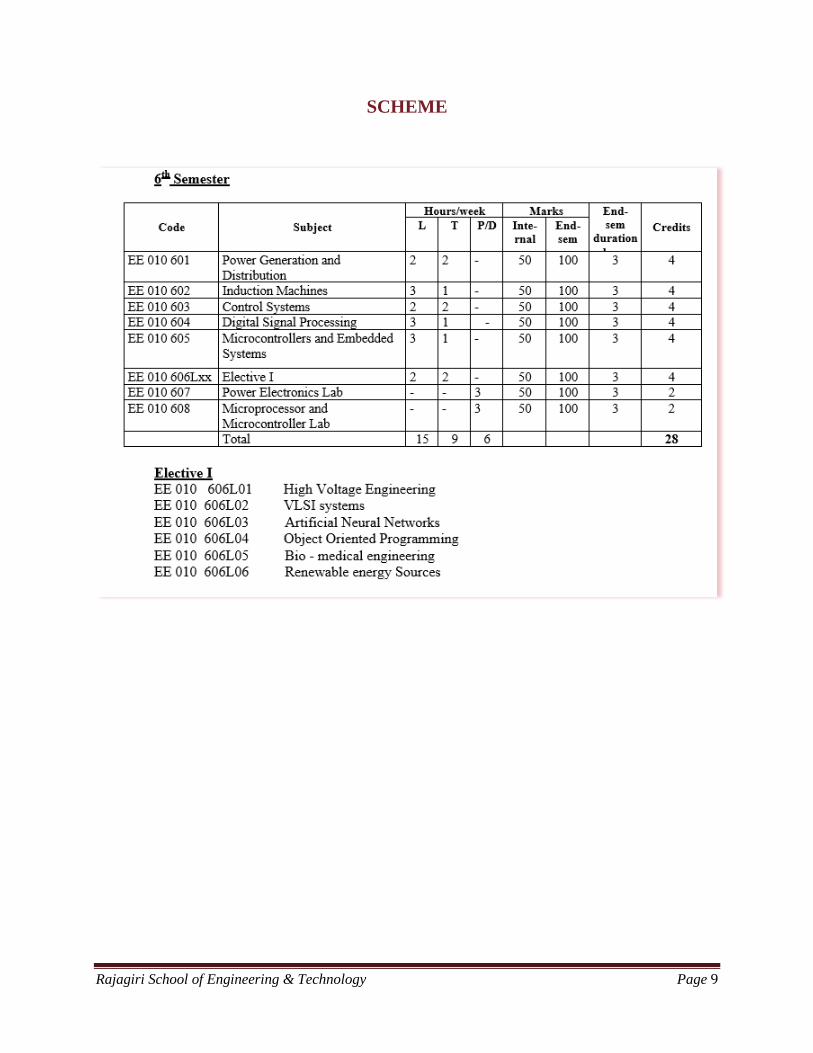
SCHEME

Rajagiri School of Engineering & Technology Page 10
ASSIGNMENT SCHEDULE
3rd
week EE 010 601 Power Generation and
Distribution
4th
week EE 010 602 Induction Machines
4th
week EE 010 603 Control System
5th
week EE 010 604 Digital Signal Processing
5th
week EE 010 605 Microprocessor and Embedded
Systems
6th
week EE 010 606 L 06 Renewable Energy
Resources
7th
week EE 010 606 L04 Object Oriented
Programming
8th
week EE 010 601 Power Generation and
Distribution
9th
week EE 010 602 Induction Machines
9th
week EE 010 603 Control System
10th week EE 010 604 Digital Signal Processing
11th week EE 010 605 Microprocessor and Embedded
Systems
11th week EE 010 606 L06 Renewable Energy
Resources
12th week EE 010 606 L04 Object Oriented
Programming

Rajagiri School of Engineering & Technology Page 11
4.1 COURSE INFORMATION SHEET
PROGRAMME: Electrical & Electronics
Engineering
DEGREE: B.TECH
COURSE: Power Generation and
Distribution
SEMESTER: VI CREDITS: 4
COURSE CODE: EE 010 601 REGULATION:
UG
COURSE TYPE: CORE
COURSE AREA/DOMAIN: Electrical Power CONTACT HOURS: 4+1 (Tutorial) hours/Week.
CORRESPONDING LAB COURSE CODE (IF
ANY): Nil
LAB COURSE NAME: Nil
SYLLABUS:
UNIT DETAILS HOURS
I
Steam power plants: Rankine cycle (ideal, actual and reheat) – layout – components –alternators – excitation system – governing system.
Hydroelectric power plants: selection of site – mass curve – flow duration curve –hydrograph – classification of hydro plants – layout – components – classification of hydro turbines.
Nuclear power plants: layout – components – pressurized water reactor – boiling water reactor – heavy water reactor – gas cooled reactor – fast breeder reactor.
Gas power plants: gas turbine cycle – layout – open cycle, closed cycle and combined cycle gas power plants.
Diesel power plants: Thermal cycle – diesel plant equipment.
12
II
Economic Aspects: Load Curve – Load duration curve – Energy load curve –
Maximum demand – demand factor – Diversity factor – coincidence factor –
contribution factor – load factor – Plant capacity factor – Plant use factor –
Utilisation factor – power factor and economics of power factor correction.
Tariffs: Flat rate tariff – Two part tariff – Block rate tariff – maximum demand
tariff – power factor tariff.
8
III
Distribution Feeders: Primary and secondary distribution – Feeder loading –
voltage drop in feeder lines with different loadings – Ring and radial distribution
– Transformer Application factor – Design considerations of distribution Feeder –
Kelvin’s law.
10
POWER GENERATION AND DISTRIBUTION EE 010 601

Rajagiri School of Engineering & Technology Page 12
IV
Voltage drop in DC 2 wire system, DC 3 wire system, AC single phase 2 wire
system, AC three phase 3 wire and 4 wire systems – voltage drop computation
based on load density – voltage drop with underground cable system – power
loss estimation in distribution systems –power factor improvement using
capacitors – sub harmonic oscillations and ferro resonance due to capacitor
banks – optimum power factor for distribution systems.
15
V
Energy Management & Auditing: The need for energy management. – Demand
side energy management – auditing the use of energy – types of energy audit –
electrical load management and maximum demand control – distribution and
transformer losses – energy savings in motors and lighting systems.
15
TOTAL HOURS 60
TEXT/REFERENCE BOOKS:
T/R BOOK TITLE/AUTHORS/PUBLICATION
T D P Kothari and I J Nagrath , Power System Engineering:, Tata McGraw Hill
R S N Singh, Electric Power Generation, Transmission and Distribution, PHI Reference Books
T V Kamaraju, Electrical Power Distribution Systems, Tata McGraw Hill
R M V Deshpande, Elements of Electrical Power Station Design, PHI
T A Chakrabarthi, M L Sony, P V Gupta, U S Bhatnagar, A Text Book on Power System Engg. ,
Dhanpat Rai & Co.
R Lucas M. Faulkenberry, Walter Coffer, Electrical power Distribution and Transmission, Pearson
Education.
R P.S. Pabla, Electric Power Distribution, Tata Mcgraw Hill
COURSE PRE-REQUISITES:
C.CODE COURSE NAME DESCRIPTION SEM
EN010 108 Basic Electrical Engineering Basic electrical components and working I
EE010 603 Induction Machines For getting idea about generator VI
EE010 303 Electrical Circuit Theory For the power circuit analysis III
EN010 102 Engineering Physics For getting an introduction about power
plants including nuclear energy
I
EN010 107 Basic Mechanical Engineering For getting an introduction about power I

Rajagiri School of Engineering & Technology Page 13
plants including diesel engine.
COURSE OBJECTIVES:
1 To impart introductory knowledge of power system.
2 To develop understanding of power generation system and power distribution system.
COURSE OUTCOMES:
SNO DESCRIPTION Blooms’ Taxonomy Level
1 Students will be able to explain different types
electrical power plants
Application [Level 3]
2 Students will be able to analyze the economic
aspects of power generation and the calculation
of electrical energy tariff
Analysis [level 4]
3 Students will be able to list out and Write the
different types of distribution system and can
perform the voltage drop computation in
distribution system
Knowledge [level 1]
4 Students will be able to classify the different
type’s secondary distribution system.
Comprehension [level 2]
5 Students will be able to relate the Energy usage
and Energy management by organizing an
Energy auditing.
Synthesis [Level 5]
MAPPING COURSE OUTCOMES (COs) – PROGRAM OUTCOMES (POs) AND COURSE OUTCOMES (COs) –
PROGRAM SPECIFIC OUTCOMES (PSOs)
PO 1 PO 2 PO 3 PO 4 PO 5 PO 6 PO 7 PO 8 PO 9 PO 10 PO 11 PO 12 PSO 1 PSO 2 PSO 3
C 601.1 2 2 1 2 1 2
C 601. 2 2 3 2 1
C601. 3 3 3 2
C601. 4 2 2 1 2
C601. 5 2 2 2 1 1 2 3 1
Rajagiri School of Engineering & Technology Page 14
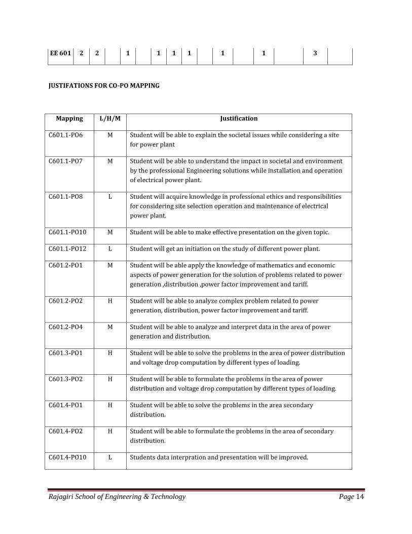
EE 601 2 2 1 1 1 1 1 1 3
JUSTIFATIONS FOR CO-PO MAPPING
Mapping L/H/M Justification
C601.1-PO6 M Student will be able to explain the societal issues while considering a site
for power plant
C601.1-PO7 M Student will be able to understand the impact in societal and environment
by the professional Engineering solutions while installation and operation
of electrical power plant.
C601.1-PO8 L Student will acquire knowledge in professional ethics and responsibilities
for considering site selection operation and maintenance of electrical
power plant.
C601.1-PO10 M Student will be able to make effective presentation on the given topic.
C601.1-PO12 L Student will get an initiation on the study of different power plant.
C601.2-PO1 M Student will be able apply the knowledge of mathematics and economic
aspects of power generation for the solution of problems related to power
generation ,distribution ,power factor improvement and tariff.
C601.2-PO2 H Student will be able to analyze complex problem related to power
generation, distribution, power factor improvement and tariff.
C601.2-PO4 M Student will be able to analyze and interpret data in the area of power
generation and distribution.
C601.3-PO1 H Student will be able to solve the problems in the area of power distribution
and voltage drop computation by different types of loading.
C601.3-PO2 H Student will be able to formulate the problems in the area of power
distribution and voltage drop computation by different types of loading.
C601.4-PO1 H Student will be able to solve the problems in the area secondary
distribution.
C601.4-PO2 H Student will be able to formulate the problems in the area of secondary
distribution.
C601.4-PO10 L Students data interpration and presentation will be improved.

Rajagiri School of Engineering & Technology Page 15
C601.5-PO1 M Student will be able to solve the problems in the area of energy
management and energy audit.
C601.5-PO2 M Student will be able to formulate the problems in the area of energy
management and energy audit.
C601.5-PO6 M Student will be able to apply the knowledge in the area of energy
management for the solution of societal issues.
C601.5-PO7 L Conduction of enengy audit helps the student for the better understnding of
socital impact of engineeing solutions in the area of energy management.
C601.5-PO8 L Will help the student for the better understading ethical princiles and
responsibilities in the area of energy management.
C601.5-PO10 M Presentation and documentation of the audit report improve the
communication ability.
C601.5-PO12 H Student will be able to apply the ideas in energy management in the future
life.
GAPS IN THE SYLLABUS - TO MEET INDUSTRY/PROFESSION REQUIREMENTS:
SNO DESCRIPTION PROPOSED
ACTIONS
RELEVANCE
WITH POs
RELEVANCE
WITH PSOs
1. For effective learning of practical operation of
the generating stations( Diesel ,Thermal
,hydroelectric Power plants)
Industrial
Visit
6 ,7,12 1,2
2 Methods of determining depreciation – Straight
line method –Diminishing value method-
Sinking fund method
Additional
class
1,2,11,12 -
3 Importance of high load factor. Additional
class
1,2,12 2
4 General awareness about the present scenario
in the state.
Additional
class
1,2,6,7,12 2
PROPOSED ACTIONS: TOPICS BEYOND SYLLABUS/ASSIGNMENT/INDUSTRY VISIT/GUEST
LECTURER/NPTEL ETC

Rajagiri School of Engineering & Technology Page 16
TOPICS BEYOND SYLLABUS/ADVANCED TOPICS/DESIGN:
SNO DESCRIPTION PROPOSED
ACTIONS
RELEVANCE
WITH POs
RELEVANCE
WITH PSOs
1 Calculation Cost of electrical energy,
Expression for cost electrical energy
Additional
class
1,2,12 2
2 Methods of determining depreciation –
Straight line method –Diminishing value
method-Sinking fund method – Tutorials.
Additional
class
1,2,11,12 2
WEB SOURCE REFERENCES:
1 KSEB Profile ,KSEB [online]
available:http://www.kseb.in/~ksebuser/index.php?option=com_content&view=article&id=58&Ite
mid=34 (Accessed on 15th Jan 2013)
DELIVERY/INSTRUCTIONAL METHODOLOGIES:
CHALK & TALK STUD. ASSIGNMENT WEB RESOURCES
LCD/SMART
BOARDS
STUD. SEMINARS ADD-ON COURSES
ASSESSMENT METHODOLOGIES-DIRECT
ASSIGNMENTS STUD. SEMINARS TESTS/MODEL
EXAMS
UNIV. EXAMINATION
STUD. LAB
PRACTICES
STUD. VIVA MINI/MAJOR
PROJECTS
CERTIFICATIONS
ADD-ON COURSES OTHERS

Rajagiri School of Engineering & Technology Page 17
ASSESSMENT METHODOLOGIES-INDIRECT
ASSESSMENT OF COURSE OUTCOMES (BY
FEEDBACK, ONCE)
STUDENT FEEDBACK ON FACULTY (TWICE)
ASSESSMENT OF MINI/MAJOR PROJECTS BY
EXT. EXPERTS
OTHERS
Prepared by Approved by
Mr. Thomas K P Ms. Santhi B
HOD EEE

Rajagiri School of Engineering & Technology Page 18
4.2 COURSE PLAN
Sl No Module Date Topic
1 1 16-Jan-17
Introduction to Various power plants. Present scenario of electrical
power generation /distribution.
2 1 17-Jan-17
Introduction to Steam power plant. Rankine cycle -Ideal ,Actual and
reheat. Layout components and working of Steam power plant.
3 1 18-Jan-17
Alternators ,Excitation System and Governing system of steam power
plant.
4 1 19-Jan-17
Hydroelectric Power Plant -Site Selection -Mass Curve- Flow duration
curve hydro graph-Classification of hydro plants
5 1 23-Jan-17
Layout ,Component and working of Hydroelectric power plant-
Classification of hydro turbines.
6 1 24-Jan-17
Nuclear Power Plants -Layout ,Component and working of Nuclear
power plant. Pressurized water reactor
7 1 25-Jan-17
Boiling water reactor -Heavy water reactor -gas cooled reactor -Fast
breeder reactor.
8 1 30-Jan-17
Gas Power Plants -gas Turbine cycle - Layout Components and working
of Gas Power plant
9 1 31-Jan-17 Open cycle ,closed cycle and combined cycle of gas power plant.
10 1 1-Feb-17 Diesel Power plant- Thermal cycle
11 1 2-Feb-17 Diesel power plant layout components and working.
12 2 6-Feb-17
Economic Aspects - Load Curve ,Load duration Curve -Energy load curve-
Maximum Demand - Demand factor - Diversity factor -coincidence factor
- contribution factor -load factor -plant capacity factor -plant use factor -
utilization factor.
13 2 7-Feb-17
Tutorial on Economic Aspects in power system generation and
distribution.
14 2 8-Feb-17
Tutorial on Economic Aspects in power system generation and
distribution.
15 2 9-Feb-17 Power factor and economics of power factor correction.

Rajagiri School of Engineering & Technology Page 19
16 2 13-Feb-17 Tutorial on Power factor and economics of power factor correction.
17 2 14-Feb-17
Tariff -Flat rate tariff -Two part tariff - Block rate tariff- maximum
demand tariff - power factor tariff
18 2 15-Feb-17
Tariff -Flat rate tariff -Two part tariff - Block rate tariff- maximum
demand tariff - power factor tariff
19 2 16-Feb-17 Tutorial on tariff
20 2 20-Feb-17 Tutorial on tariff
21 2 21-Feb-17 Tutorial on tariff
22 3 22-Feb-17
Distribution Feeders - Primary secondary distribution -feeder loading -
voltage drop in feeder lines with different loading.
23 3 23-Feb-17 Tutorial on feeder loading
24 3 27-Feb-17 Tutorial on feeder loading
25 3 28-Feb-17 Tutorial on feeder loading
26 3 1-Mar-17 Ring and radial distribution -Transformer application factor
27 3 2-Mar-17 Design considerations of distribution feeder - Kelvin's law.
28 3 6-Mar-17 Tutorial on feeder design.
29 3 7-Mar-17 Tutorial on feeder design.
30 3 8-Mar-17 Tutorial on feeder design.
31 3 9-Mar-17 Tutorial on feeder design.
32 4 20-Mar-17
Voltage drop in DC 2 wire system, DC 3 wire system, AC single phase 2
wire system, AC three phase 3 wire and 4 wire systems.
33 4 21-Mar-17
Tutorial on Voltage drop in DC 2 wire system, DC 3 wire system, AC
single phase 2 wire system, AC three phase 3 wire and 4 wire systems.
34 4 22-Mar-17
Voltage drop computation based on load density – voltage drop with
underground cable system – power loss estimation in distribution
systems .
35 4 23-Mar-17
Tutorial on voltage drop computation based on load density – voltage
drop with underground cable system – power loss estimation in
distribution systems.
Rajagiri School of Engineering & Technology Page 20
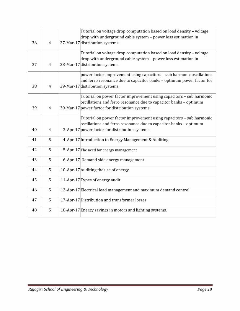
36 4 27-Mar-17
Tutorial on voltage drop computation based on load density – voltage
drop with underground cable system – power loss estimation in
distribution systems.
37 4 28-Mar-17
Tutorial on voltage drop computation based on load density – voltage
drop with underground cable system – power loss estimation in
distribution systems.
38 4 29-Mar-17
power factor improvement using capacitors – sub harmonic oscillations
and ferro resonance due to capacitor banks – optimum power factor for
distribution systems.
39 4 30-Mar-17
Tutorial on power factor improvement using capacitors – sub harmonic
oscillations and ferro resonance due to capacitor banks – optimum
power factor for distribution systems.
40 4 3-Apr-17
Tutorial on power factor improvement using capacitors – sub harmonic
oscillations and ferro resonance due to capacitor banks – optimum
power factor for distribution systems.
41 5 4-Apr-17 Introduction to Energy Management & Auditing
42 5 5-Apr-17 The need for energy management
43 5 6-Apr-17 Demand side energy management
44 5 10-Apr-17 Auditing the use of energy
45 5 11-Apr-17 Types of energy audit
46 5 12-Apr-17 Electrical load management and maximum demand control
47 5 17-Apr-17 Distribution and transformer losses
48 5 18-Apr-17 Energy savings in motors and lighting systems.

Rajagiri School of Engineering & Technology Page 21
4.3 ASSIGNMENT
Assignment No 1
1. Explain about the following nuclear reactor (i) Pressurized water reactor (PWR) (ii) Boiled water reactor (BWR) (iii) Heavy water cooled and moderator reactor (CANDU Type) (iv) Gas cooled reactor (GCR) (v) Fast breeder reactor (FBR)
2. Explain Gas Turbine Cycles
Assignment No 2
1. What are the needs for energy management? 2. Explain demand side energy management. 3. Explain the auditing in the use of energy management. 4. Explain different types of energy management. 5. Explain electrical load management and maximum demand control 6. Describe distribution and transformer losses. 7. Explain energy saving in motor and lighting system.
4.4 TUTORIAL QUESTIONS
Module II
Economic Aspects
1. Maximum demand on a power station is 100MW. Annual load factor is 40%. Calculate total energy generated in a year.
2. A generating station has a connected load of 43MW and maximum demand of 23MW. The unit generated being 61.5X10⁶/annum. Calculate demand factor and load factor.
3. A 100MW power station delivers 100MW for two hours 50MW for 6Hours and is shut down for maintenance 45 days each year. Calculate annual load factor.
4. A Generating station has maximum demand of 25MW. A load factor of 60%. Plant capacity factor of 50% and plant use factor is 72%.

Rajagiri School of Engineering & Technology Page 22
(i) Reserve capacity (ii) Daily energy produced (iii) Maximum energy produced daily if plant running as per schedule where fully
loaded. 5. A diesel station supplies following load to consumers
(i) industrial -1500kW (ii) commercial 750kW (iii) domestic power 100kW (iv) domestic light 450kW
if maximum demand of station is 2500kW and number of kWh generated per year is
45X105. Determine diversity factor and annual load factor.
6. A power station has a maximum demand of 150000kW. Annual load factor 50%. Plant capacity factor 40%. Find reserve capacity.
7. A generating station has following daily load cycle Time Hours: 0-6 6-10 10-12 12-16 16-20 20-24
Load MW: 40 50 60 50 70 40
Draw load curve and find the (i) maximum demand (ii) unit generated per day (iii) average
load (iv) load factor . Also draw load duration curve.
8. A power station has to meet the following demands
Time Hours: 0-6 6-8 8-10 10-18 18-24 max demand
Group A: 200 200 200
Group B: 100 100 100
Group C: 50 50 50
Group D: 100 100 100 100
Plot daily load curve and determine (i) diversity factor (ii) unit generated per day (iii) load
factor
9. Daily demand of 3 consumers are given below Time I II III Total load
12.00-8AM 200W 200W
8AM-2PM 600W 200W 800W
2PM-4PM 200W 1000W 1200W 2400W
4PM-10PM 800W 800W

Rajagiri School of Engineering & Technology Page 23
10PM-12.00 200W 200W 400W
Plot load curve, find the maximum demand and individual consumers. Load factor of
individual consumers, diversity factor, and load factor of the station.
10. A power station has daily load cycle 260MW for 6 hours 200MW for 8 hours 160MW for 4 hours 100MW for 6hours. If power station is equipped with 4 sets 75 MW each. Calculate (i) daily load factor (ii) plant capacity factor (iii) daily requirement if calorific value of oil used is 10000kcal/kg and average heat rate of station is 2860 kcal /kWh
11. Annual load duration curve of a station can be considered as a straight line from 20MW to 40MW. To meet the slope 3 turbine –generator unit two rated at 10MW each and rated one at 5MW.Determine installed capacity. Find (i)Plant factor (ii) units generated per annum (iii) load factor (iv) utilization factor
Tariff
1. A consumer has maximum demand of 200kW at a 40% load factor. If tariff is Rs.100/kW of maximum demand plus 10paise /kWh. What is the overall cost per kW.
2. Maximum demand of consumers is 20A at 220V and total energy consumption is 8760kWh. If energy is charged at rate of 20paise/unit for 500hours of use of maximum demand /annum plus 10paise/unit for additional unit. Calculate (i) annual bill (ii) equivalent flat rate
3. Following two tariffs are offered (i) Rs.100+15paise/unit . (ii) A flat rate of 30paise/unit. At what consumption first tariff is
economical.
4. A supply is offered on the basis of fixed charge of Rs.30/annum +30 paise/unit or alternatively at a rate of 6 paise/unit for first 400 unit/annum and at 5paise/unit for additional units. Find the number of units taken per annum for which the cost under two tariff become equal.
5. An electric supply having maximum demand of 50MW generate 18X107/annum and supply consumes have an average aggregate demand of 75MW. Annual expenses including capital charges are (i) for fuel Rs.90 Lakh (ii) fixed charges concerning generation Rs.28Lakh (iii) fixed charges concerning transmission and distribution Rs.32Lakh. Assuming 90% fuel cost is essential to running charges and loss in transmission and distribution as 15% of kW generated. Deduce a two part tariff to find actual cost of supplied unit to the consumer.
6. A generating station has maximum demand of 75MW and yearly load factor of 40%. Generating power inclusive of station capital cost are Rs.60/annum/kW demand plus 4paise/kWh transmitted. The annual capital charges for transmission charges are rs.20Lakhs and for distribution system Rs.15Lakhs.Respective diversity factor is 1.2 and 1.25. Efficiency of transmission system is 90% and that of distribution system inclusive of substation losses is 85%. Find yearly cost per kW demand and cost/kWh supply (i) at substation (ii) at consumer end.
7. Determine load factor at which cost of supplying a unit of electricity by a diesel and steam station is same. If the fixed annual and running charges are as follows. Station Fixed charge Running charges

Rajagiri School of Engineering & Technology Page 24
Diesel 300/kW 2.5 paise/kWh
Steam 1200/kW 6.25 paise/kWh
8. Calculate the annual bill of a consumer whose maximum demand is 100kW power factor 0.8lag and load factor 50%. Tariff used is Rs.75/kVA of maximum demand plus 15 paise/kWh.
9. A factory has maximum load of 240kW at 0.8pf lag. If annual consumption of 50000 units. Tariff is 50/kVA of maximum demand plus 10paise/unit. Calculate flat rate tariff for the energy consumption. What will be the annual saving if pf is increased to unity.
10. A generating station has two 1000kW diesel generator sets. Load is estimated to reach a maximum demand of 2500kW. After two years with an increase of 5.5X10⁶ units over the present value. To meet this demand following two alternatives are available. Purchasing one more set of 1000kW at Rs.400/kW. The annual interest of depreciation of
new set are 10% of capital investment. Cost of generation for the station is Rs.75/kW
maximum demand +5paise/kWh
Purchasing bulk power from grid supply at Rs.120 /kW of maximum demand +3paise/kWh.
Find which is cheaper and by howmuch.
Power factor and Economics of power factor correction
1. An alternator supplying a load of 300kW at a pf of 0.86lag. If pf is raised to unity how many more kW can alternator supply for the same kVA loading.
2. A single phase motor connected to a 400V ,50Hz supply takes 31.7A at pf 0.7lag. Calculate capacitance required in parallel with motor to raise pf 0.9 lag.
3. A single phase AC generator supplying a following load. (i) Light load of 20kW at pf unity. (ii) Induction machine load of 100kW at pf 0.707 lag. (iii) Synchronous motor load of 50kW at 0.9 lead.
Calculate total kW and kVA delivered by generator and pf at which it works.
4. A 3 phase 5kW induction motor has a pf of 0.75 lag. A bank of capacitor connected in delta across terminals and pf raised to 0.9 lag. Determine kVAr rating of capacitor connected in each phase.
5. Load on a generating station is 800kW 0.8 pf lag which works for 3000hours/annum. Tariff is Rs.100/kVA +20 paise/kWh. If pf is improved to 0.9 lag by means of losses free capacitor costing Rs.60/kVAr. Calculate annual saving affected. Allotted 10% /annum for depreciation on capacitor.
6. A factory takes a load of 200kW at 0.85pf lag for 2500hours/annum. Tariff is Rs.150/kVA+5paise/kWhr. If pf is improved to 0.9lag by means of capacitor costing Rs.420/kVAr and having a power loss of 100W /kVAr. Calculate annual saving affected. Allow 10% /annum depreciation.

Rajagiri School of Engineering & Technology Page 25
Module III
1. A two wire DC distributor cable AB 2km long and supplies a load of 100A,150A,200A and 50A located at 500m,1000m,1600m amd 2000m from end A. Each conductor has a resistance of 0.01 ohm/1000m. Calculate voltage drop at each load point. Voltage at feeding point is 300V.
2. A 2 wire DC distribution AB is 300m long. It is fed at point A. The various loads and their positions are given below. At point Distance from A Load
C 40m 30A
D 100m 40A
E 150m 100A
F 250m 50A
Maximum permissible voltage not exceeded 10V. Find the cross sectional area of the
distributor. Take ρ= 1.78X10⁻⁸ohm meter.
3. Two tramp cars A and B ,3 and 6 km away from substation returns 40m and 20 A to rail. The substation voltage is 600V. Resistance of the trolley wire is 0.2 ohm/km and track is 0.03 ohm/km. Calculate voltage across each 2 tramp cars.
4. Load distribution of a 2 wire DC distributor has cross sectional area of each conductor 0.27 cm2. The end A is supplied at 250V. Resistivity of wire is ρ= 1.78X10⁻⁸ohm meter. Find (i) current in each section (ii) resistance of each section (iii) voltage at tapping point.
5. A 2 wire DC distributor 200 m long is uniformly distributed with 2A/m. Resistance of single wire is 0.3ohm/km. If distributor is fed at one end. Find (i) voltage drop at a distance of 150m from fed point (ii) Maximum voltage drop.
6. A uniform 2 wire DC distributor has 500m long is loaded with 0.4A/m and is fed at one end. If maximum permissible voltage drop cannot exceed 10V. Find the cross sectional area of the distributor conductor. Take ρ= 1.7X10⁻⁸ohm meter.
7. A 250 m 2 wire DC distributor loaded uniformly at a rate of 1.6A/m. The resistance of each conductor is 0.00002 ohm/m. Find the voltage at feed point to maintain voltage (i)at far end (ii)at mid point of the distributor.
8. Calculate voltage at 200m of 300 long distributor uniformly loaded at 0.75A/m. Distributor is fed at one end at 250V. Resistance of distributor go and return per meter is 0.00018 ohm/m. Also find power loss in distributor.
9. A two wire DC street mains AB 600m long is fed from both ends at 200V. Loads of 20A ,40A, 50A and 30A are tapped at a distance of 100m,250m,400m and 500m from end A respectively. If the area of cross section of distributor is 1cm2. Find minimum consumer voltage. Take ρ= 1.7X10⁻⁸ohm meter.
10. A 2 wire DC distributor AB is fed from both ends at A voltage is maintained as 230V and at B 235V. Total length of the distributor is 200m. Loads are tapped out as under Load length from end A

Rajagiri School of Engineering & Technology Page 26
25A 50m
50A 75m
30A 100m
40A 150m
Resistance/km one conductor is 0.3ohm. Calculate current in various segments ,minimum
voltage and point at which it occurs.
11. A 2 wire DC distributor cable 1000m long is loaded with 0.5A/m. Resistance of each conductor is 0.05ohm/km. Calculate maximum voltage drop if distributor is fed from both ends with equal voltages of 220V. What is the minimum voltage and where it occurs.
12. A 2 wire DC distributor AB 500m is fed from both ends and is loaded uniformly at a rate of 1A/m. At A voltage is 255V and at B voltage is 250V. If resistance of each conductor is 0.1ohm/km. Determine minimum voltage and maximum voltage drop.
13. A 800m 2 wire DC distributor AB fed from both ends uniformly loaded at a rate of 1.25A/m. Calculate voltage at point A and B if minimum potential of 220V occurs at point C at distance 450m from A. Resistance R is 0.05ohm/km.
14. A 2 wire DC distributor cable 900m long is fed at 400V and loads of 50A ,100A and 150A are tapped off from points C,D and E which are at a distance of 200m, 500m and 800m from point A respectively. The distributor is also loaded uniformly at a rate of 0.5A/m. If resistance of distributor per meter (both go and return) is 0.0001ohm/m. Calculate voltage (i) at point B (ii) at point D.
15. A 2 wire DC distributor AB =1000m, resistance r=0.1ohm. voltage at A and B are equal 240V. The distributor is uniformly loaded at 0.5ª/m and has loads 120A ,60A, 100A and 40A at 200m,400m,700m and 900m from A. Calculate (i) point of ,minimum current (ii)current in each segment (iii)value of minimum voltage.
16. A 2wire DC distributor AB 500m long fed at both ends 240V. Distributor is loaded at both ends. Resistance of distributor is 0.001 ohm/m. Calculate (i) minimum voltage (ii)value of the current from point B.
17. A 2 wire DC ring distributor is 300m long is fed 240V at point A. At point B 150m from A, a load of 120A is taken at C 100m opposite direction a load of 80A is taken. If resistance /100m of single conductor is 0.03ohm. Find (i)current in each section (ii) voltage at B and C.
18. A 2wire DC distributor ABCDEA main at point A 220V and is loaded as under. 10A at B ,20A at C, 30A at D, 10A at E. Resistance of various section go and return are AB =0.1ohm BC=0.05ohm CD=0.01ohm DE=0.025ohm EA=0.07 ohm. Find point of minimum potential and point at which occurs.
19. A DC ring type ABCDEA is fed at point A from a 250V supply. Resistance includes both go and return of various section are as follows AB=0.02ohm BC=0.018 ohm CD=0.025ohm DA =0.02ohm. The main supply is loaded 150 A at B,300A at C and 250A at D. Determine voltage at each load point. If A and C are lined through inter connection of R=0.02 ohm. Determine new voltage at each load point.
20. AB cable 1km long is required to supply constant current of 200A through out the year. The cost of cable including insulation is Rs.20a+20/m where a is the area of cross section in cm2. Cost of energy is 5paise/kWh and interest and depreciation charges amount 10%. Calculate most economical size of conductor. Assume ρ=1.7μ ohm cm.

Rajagiri School of Engineering & Technology Page 27
Module IV
1. A load supplied on 3 wire DC system takes a current of 50A on positive side and 40A on negative side. Resistance of each outer wire is 0.1ohm and cross sectional area of middle wire is half of that of outer. If system is supplied with 500/250V. Find voltage at load end between outer and middle.
2. A 3 wire DC distributor system supplies a load of 5ohm resistance across positive and neutral , 6ohm resistance across negative and neutral. Resistance of each conductor is 0.1ohm. if voltage between outer and neutral at load end is to be kept to 240V. Find the feeding end voltage.
3. A 3wire 500/250V distribution system AB 600m long is supplied at end A and is loaded as under +ve side : 60A 200m from A 40A 30m from A
-ve side :20A 100m from B 60A 260m from B 15A 600m from B.
Resistance of each outer is 0.02 ohm /100m and cross sectional area of neutral wire same
as outer. Find voltage across each load.
4. A DC 3 wire system with 500V between the outer supplies 1500kW at +ve outer end and 2000kW at –ve outer. If the losses in machine are neglected. Calculate (i) current at neutral (ii)current supplied by main generator (iii)current supplied by balances machines.
5. A DC 3 wire system with 500V between the outer supplies light loads of 150kW at +ve outer end and 100kW at –ve outer. If the losses in machines is 3kW. Calculate (i) Total load on the main generator (ii) kW loading of each balances machines.
6. A single phase AC distributor AB 300m long is fed from end A and is loaded as under (i) 100A at 0.707pf lag 200m from end A (ii)200A at 0.8pf lag 300m from end A. Resistance and reactance of distributor is 0.2ohm and 0.1ohm per km. calculate voltage drop in distributor. Load power factor refers to the voltage at far end.
7. A single phase 2km long supplies load of 120A at 0.8 pf lag at its far end and a load of 80A 0.9pf lag at its mid point. Both pf are referred to the voltage at far end. Resistance and reaction /km both go and return are 0.05 ohm ,0.1ohm respectively. If voltage at far end is maintained at 230V. Calculate (i)voltage at sending end (ii) phase angle between voltage at two ends.
8. A single phase distributor ABC id fed at A. loads at B and C are 20A at 0.8pf lag and 15A at 0.6 pf lag respectively. Both expressed with reference to voltage at A. Total impedance of 3 sections AB ,BC and CA are (1+j1) ,(1+j2) and (1+j3) respectively. Find the total current fed at A and current in each sections.
9. A 3 phase ABCD fed at 11kV at point A supplies balanced load of 50A at 0.8pf lag at B, 120A upf at C, 70A at 0.866lag at D. Load currents being reflected to supply voltage at A. Impedances of various sections are AB=1+j0.6 BC=1.2+j0.9 CD=0.8+j0.5 DA=3+j2 .Calculate current and bus bar voltage in C ,C and D.
10. Non reactive loads of 10kW ,8kW and 5kW are connected between R Y B phases respectively. Line voltage is 400V. Calculate (i) Current in each line (ii) Current in neutral line.
11. A 3 phase 4 wire system provides power at 400V and lighting at 230V. If lamps used require 70 ,84 and 33A in each of 3 lines. What could be current in neutral line? If 3phase motor is now started taking 200A from the lines at pf of 0.2lag, what will be the total current in each line and neutral line? Find also total power supplied to lamp and motor.

Rajagiri School of Engineering & Technology Page 28
5.1 COURSE INFORMATION SHEET
PROGRAMME: Electrical and Electronics DEGREE: B.Tech
COURSE: Induction Machines SEMESTER: Six CREDITS: 4
COURSE CODE: EE 010 602 REGULATION:UG COURSE TYPE: Core
COURSE AREA/DOMAIN: Electrical Machines CONTACT HOURS: 3 (Lecture) +1 (Tutorial)
Hours/Week.
CORRESPONDING LAB COURSE CODE (IF ANY): EE 010
806
LAB COURSE NAME: Electrical Machines Lab II
SYLLABUS:
UNIT DETAILS HOURS
I Three phase induction motor: Construction-squirrel cage and slip ring motors principle of operation-slip and frequency of rotor current-mechanical power - developed torque- phasor diagram-torque-slip curve-pull out torque-losses and efficiency. No load and locked rotor tests-equivalent circuit-performance calculation from equivalent circuit-circle diagram-operating characteristics from circle diagram-cogging and crawling and methods of elimination.
16
II Starting of three phase squirrel cage induction motor-direct on line starting-auto transformer star delta starting- starting of slip ring motors-design of rotor rheostat-variation of starting torque with rotor resistance. Speed control-pole changing-rotor resistance control-frequency control-static frequency conversion-Deep bar and double cage induction motor –equivalent circuit -applications of induction machines-single phasing-analysis using symmetrical components.
14
III Induction Generator: Theory- phasor diagram-Equivalent circuit-Synchronous Induction motor-construction-rotor winding connections-pulling into step Single phase Induction motor: Revolving field theory- equivalent circuit- torque-slip curve starting methods-split phase, capacitor start-capacitor run and shaded pole motors.
10
IV Commutator motors-principle and theory-emf induced in a commutator winding- Single phase series motor :theory –phasor diagram-compensation and interpole winding-Universal motor-Repulsion motor: torque production –phasor diagram-compensated type of motors repulsion start and repulsion run induction motor-applications-Reluctance motor-Hysterisis motor. 10
V Construction-principle of operation, operating characteristics of stepper motor, switched reluctance motor, BLDC motor, Permanent magnet synchronous motor, linear induction motor-principle-application-magnetic levitation
10
TOTAL HOURS 60
INDUCTION MACHINES EE010 602

Rajagiri School of Engineering & Technology Page 29
TEXT/REFERENCE BOOKS:
T/R BOOK TITLE/AUTHORS/PUBLICATION
T.1 Alexander Langsdorf A S, Theory of AC Machinery, Tata McGraw-Hill
T.2 Dr. P S Bimbhra, Electrical Machinery, Khanna Publishers
R.1 Say M G, Performance and design of AC Machines, ELBS
R.2 J B Gupta, Electrical Machines , S K Kataria and Son
R.3 Nagarath I J and Kothari D P, Electrical Machines ,4e, Tata McGraw- Hill Education, New Delhi, 2010
R.4 Vincent Deltoro, Electrical Machines and Power System, Prentice Hall
R.5 Venketaratnam, Special Electrical Machines, Universal Press
COURSE PRE-REQUISITES:
C.CODE COURSE NAME DESCRIPTION SEM
EE0101
08
Basic Electrical Engineering Basic idea on electromechanical energy
conversion and fundamental concepts of AC.
1 and
2
EE0104
02
DC Machines and Transformers Knowledge about construction and working
principle of DC machines and transformers.
4
COURSE OBJECTIVES:
1 To impart concepts about construction, working principle and performance studies of Induction Machines
2 To impart knowledge about construction, working principle and performance studies of commutator motors.
3 To develop a brief idea about construction, working principle and characteristics of Special Machines
COURSE OUTCOMES:
SNO DESCRIPTION BLOOM’S TAXONOMY LEVEL
1 Ability to analyse the performance characteristics of Induction
machines to get best results in household as well as industrial
applications
Analyze [level 4] a,b,c,d,e,i
,k
2 Ability to apply easier and efficient starting and speed control
methods of induction machines using power electronics.
Apply [level 3] a,b,c,e,i,k
3 Ability to understand the performance characteristics of Synchronous
Induction Machines combining the features of synchronous machines
and induction machines
Understand[level 2] a,b,c,e,i
4 Ability to explain the performance and applications of different types
of commutator machines.
Understand [level 2] a,b,c,e,i
5 Ability to describe how special machines can effectively replace
conventional Induction Machines and DC machines in industry for
efficient operation.
Understand [level 2] a,b,c,e,i
MAPPING COURSE OUTCOMES (COs) – PROGRAM OUTCOMES (POs) AND COURSE OUTCOMES (COs) – PROGRAM SPECIFIC OUTCOMES (PSOs)

Rajagiri School of Engineering & Technology Page 30
PO 1
PO 2
PO 3
PO 4
PO 5
PO 6
PO 7
PO 8
PO 9
PO 10
PO
11 PO 12
PSO 1 PSO 2
PSO 3
C 602.1 3 3 3 3 3 3 3
C 602. 2 3 2 2 3 2 2 3
C 602. 3 3 1 2
C 602. 4 3 0
C 602. 5 3 1 2 5 3 3
EE 602 3 1.4 1.4
0.6 1.6 0 1.4 0 0 0 0 1.6 1.8
JUSTIFICATIONS FOR CO-PO MAPPING
Mapping L/H/M Justification
C 602.1-PO1 H Student will be able to explain the working principle of Induction machines using
engineering fundamentals
C 602. 2-PO1 H Student will be able to explain the starting and speed control methods of Induction
motors using engineering fundamentals
C 602. 3-PO1 H Student will be able to explain the working principle of Synchronous Induction
machines using engineering fundamentals
C 602. 4-PO1 H Student will be able to explain the working principle of commutator machines using
engineering fundamentals
C 602. 5-PO1 M Students will be able explain the working principle of special electrical machines
using engineering fundamentals
C 602.1-PO2 H Students will be able to identify and analyse Engineering problems in three phase
induction machines
C 602. 2-PO2 M Students will be able to identify and analyse Engineering problems
C 602. 3-PO2 L Students will be able to identify Engineering problems in single phase induction
machines
C 602. 5PO2 M Students will be able to identify Engineering problems in special electrical
machines
C 602.1-PO2 H Students will be able to identify and analyse problems based on Induction Machines
C 602. 2-PO2 M Students will be able to identify and analyse problems based on Speed control of
Induction Machines
C 602. 3-PO2 L Students will be able to identify and analyse problems based on Single Phase
Induction Machines
C 602. 5PO2 L Students will be able to identify and analyse problems based on Special Machines
C 602.2-PO3 H Students will be able to solve problems based on Induction Machines
C 602.5-PO3 L Students will be able to solve problems based on Special Machines
C 602.2-PO5 H Students will be able to perform experiments on three phase induction machines
using Simulation tools
C 602.3-PO5 L Students will be able to perform experiments on Special electrical machines using
Simulation tools
C 602.2-PO7 H Energy saving is possible using VFD drives
C 602.5-PO7 H High efficiency drive can be designed for special machines

Rajagiri School of Engineering & Technology Page 31
C 602.2-PO12 H Continuous improvement done in starting and speed control of Induction machines
C 602.5-PO12 H Continuous improvement done in Special Electrical Machines and drives
GAPS IN THE SYLLABUS - TO MEET INDUSTRY/PROFESSION REQUIREMENTS:
SNO DESCRIPTION PROPOSED
ACTIONS
1 Simulation studies for speed control of induction machines and Special
machines not included
Can include simulation studies
using software tools like
MATLAB/SIMULINK
PROPOSED ACTIONS: TOPICS BEYOND SYLLABUS/ASSIGNMENT/INDUSTRY VISIT/GUEST LECTURER/NPTEL ETC
TOPICS BEYOND SYLLABUS/ADVANCED TOPICS/DESIGN:
1 Circle Diagram of Synchronous Induction motor
WEB SOURCE REFERENCES:
[1] Muhammad H. Rashid(2001), Power Electronics Handbook, Academic Press .
[2] Reston Condit,(2004).,Microchip Technology Inc [Online]. Available: http://www.microchip.com
DELIVERY/INSTRUCTIONAL METHODOLOGIES:
CHALK & TALK STUD. ASSIGNMENT WEB RESOURCES
LCD/SMART BOARDS STUD. SEMINARS ADD-ON COURSES
ASSESSMENT METHODOLOGIES-DIRECT
ASSIGNMENTS STUD. SEMINARS TESTS/MODEL EXAMS UNIV. EXAMINATION
STUD. LAB PRACTICES STUD. VIVA MINI/MAJOR PROJECTS CERTIFICATIONS
ADD-ON COURSES OTHERS
ASSESSMENT METHODOLOGIES-INDIRECT
ASSESSMENT OF COURSE OUTCOMES (BY FEEDBACK,
ONCE)
STUDENT FEEDBACK ON FACULTY (TWICE)
ASSESSMENT OF MINI/MAJOR PROJECTS BY EXT. EXPERTS OTHERS
Prepared by Approved by
Ms. Caroline Ann Sam Ms. Santhi B.
HOD ,EEE

Rajagiri School of Engineering & Technology Page 32
5.2 COURSE PLAN
Day Date Module Topic
20-Jan-17 Friday 1 Introduction to CIS
27-Jan-17 Friday 1 Construction ,squirrel cage and slip ring IM
30-Jan-17 Monday 1
principle of operation,slip and frequency of rotor current
31-Jan-17 Tuesday 1 Mechanical power ,developed torque, problems
1-Feb-17 Wednesday 1 torque slip curve
2-Feb-17 Thursday 1 Losses and efficiency,
3-Feb-17 Friday 1 Phasor Diagram, Equivalent circuit
6-Feb-17 Monday(T) 1 Tutorials on module 1
7-Feb-17 Tuesday 1 No load test
8-Feb-17 Wednesday 1 Stator resistance test, Blocked rotor test
9-Feb-17 Thursday 1 Problems
10-Feb-17 Friday 1 Circle Diagram
13-Feb-17 Monday(T) 1 Circle Diagram-tutorial
14-Feb-17 Tuesday(T) 1 Circle Diagram-tutorial 15-Feb-17 Wednesday 2 Starting of IM,DOL
16-Feb-17 Thursday 2 Stator Resistance starting
17-Feb-17 Friday 2 Autotransformer starting
20-Feb-17 Monday(T) 2 star Delta starting, Problems
21-Feb-17 Tuesday 2
Starting of slip ring IM-design of rotor resistance
22-Feb-17 Wednesday 2
Problems ,Variation of starting torque with rotor resistance
23-Feb-17 Thursday 2
Speed control -changing supply frequency-changing applied voltage
27-Feb-17 Monday 2
Speed control-changing number of poles-changing rotor circuit resistance-cascade operation
28-Feb-17 Tuesday 2 Single phasing-problems
1-Mar-17 Wednesday 3
Induction generator-Theory-Phasor Diag-Equivalent circuit
2-Mar-17 Thursday 3
Synchronou Induction Motor-Construction-Rotor winding connection-Pulling into step
6-Mar-17 Monday 2 Speed control-Problems

Rajagiri School of Engineering & Technology Page 33
7-Mar-17 Tuesday 3 Single phase IM-Revolving Field theory
8-Mar-17 Wednesday 3
torque slip curve,Starting methods-split phase,capacitor start
9-Mar-17 Thursday 3 Capacitor run and shaded pole type motors
15-Mar-17 Wednesday 3
EMF induced in a commutator winding-Problems
16-Mar-17 Thursday 3
Single phase series motor-Theory ,phasor diagram
17-Mar-17 Friday 3 Compensaton and interpole winding
20-Mar-17 Monday(T) 3 Tutorials on Single Phase Induction Motor
21-Mar-17 Tuesday 4 Universal motor
22-Mar-17 Wednesday 4
Repulsion Motor-torque production ,phasor diagram-compensated type of motors
23-Mar-17 Thursday 4
Repulsion start and repulsion run IM-Applications
27-Mar-17 Monday 4
Stepper motor-Construction-Principle of Operation
28-Mar-17 Tuesday 4 Tutorials on Stepper Motor
29-Mar-17 Wednesday 5 Switched Reluctance Motor
30-Mar-17 Thursday 5 Switched Reluctance Motor
31-Mar-17 Friday
3-Apr-17 Monday 5 BLDC motor
4-Apr-17 Tuesday 5 BLDC motor
5-Apr-17 Wednesday 5 Permanent magnet Synchronous motor
6-Apr-17 Thursday 5 Permanent magnet Synchronous motor
10-Apr-17 Monday(T) 5 Problems on Special machines
11-Apr-17 Tuesday 5 Linear Induction Motor-Principle -Application
12-Apr-17 Wednesday 5 Magnetic Levitation-Tutorials

Rajagiri School of Engineering & Technology Page 34
13-Apr-17 Thursday 1 ,2,3 Revision on Induction machines-
17-Apr-17 Monday 4,5 Revison on special machines-
18-Apr-17 Tuesday
Previous year QP discussion
5.3 ASSIGNMENT
Assignment 1
1. What is cogging and crawling in a three phase Induction motor? What are the methods of
elimination?
2. A 12 pole, 3 phase alternator is coupled to an engine running at 500 r.p.m. It supplies an
Induction motor which has a full load speed of 1440 r.p.m. Find the slip and no: of poles
of the motor?
3. The frequency of emf in the stator of a 4 pole Induction Motor is 50 Hz and that in the
rotor is 1.5Hz. What is the slip and at what speed the motor is running?
4. A 3 phase, 6 pole, 50 Hz, Induction Motor has a slip of 1% at no-load and 3% at Full
load. Determine (a) Synchronous speed (b) no-load speed (c) full load speed (d)
frequency of rotor current at standstill (e) frequency of rotor current at full load.
5. A 6 pole, 50 Hz, 3 phase Induction Motor delivers a shaft torque of 108.3 Nm at full load
and running at 970 rpm. Calculate (i) rotor copper loss (ii) power input to the rotor.
Mechanical losses account for 120W.
Assignment 2
1. Write short notes on (a) Hysterisis Motor (b) Reluctance Motor.
2. With a neat tabular column compare the applications of different types of
a. Three phase Induction Motor
b. Single Phase Induction Motor
3. With a neat tabular column compare the applications of
a. Commutator motors
b. Stepper Motor
c. Switched Reluctance Motor

Rajagiri School of Engineering & Technology Page 35
d. Brushless DC Motor
e. Linear Induction Motor
5.4 TUTORIAL
Module 1
6. A 3000V, 24 pole, 50 Hz, 3 phase, Y connected Induction Motor has a slip ring rotor of
resistance 0.016 Ω and standstill reactance of 0.265 Ω per phase. Full load torque is
obtained at a speed of 247 rpm. Calculate the (i) the ratio of maximum torque to full load
torque (ii) speed at maximum torque. Neglect stator impedance
7. The power input to a 4 pole, 50 Hz, 3 phase Induction Motor is 42 kW, the speed being
1455 r.p.m. The stator losses are 1.2 kW and mechanical losses are 1.8 kW. Find (a) the
rotor input (b) rotor copper loss (c) ŋ
8. A 400V, 4 pole, 50 Hz, 3 phase delta connected Induction Motor gave the following
results on no-load and short circuit tests.
No-load Test (line values) 400V 3A 645W
Short circuit Test (line values) 200V 12A 1660W
The friction and windage losses amount to 183W. Determine the working and the
magnetizing components of no-load current, no-load p.f., no-load resistance Ro and reactance
Xo, equivalent resistance and reactance per phase as referred to primary, power factor on short
circuit and short circuit current with normal applied voltage of 400V across the stator. Stator
resistance may be assumed to be 5 Ω. Also draw the appr. equivalent ckt. referred to stator.
9. A 20 h.p., 400V, 50 Hz, three phase star connected Induction Motor gave the following
test results. Assume 4 pole.
No load Test : 400V 9A p.f. – 0.2
Blocked rotor test : 200V 50A p.f. – 0.4
Stator and rotor copper losses were equal in the blocked rotor test. Draw the circle diagram
and determine at Full load (i) Line Current (ii) p.f. (iii) Speed (iv) Efficiency
Module 2
1. Determine the suitable tapping on an auto transformer starter for an Induction Motor
required to start the motor with 36% of the full load torque. The short circuit current of the
motor is 5 times the full load current and full load slip is 4%. Also determine the current in
the supply leads as a percentage of full load current.
2. A 3 phase Squirrel cage Induction motor has a starting current 175% of full load line current
and develops 35% of full load torque when operated by a star-delta starter. What should be
the starting torque and current if an auto transformer starter with 80% tapping is employed?

Rajagiri School of Engineering & Technology Page 36
Module 3
1. A 2 pole 240V, 50Hz single-phase induction motor has the following constants referred
to stator:
R1 = 2.2 Ω, X1 = 3.0 Ω, R2‟ = 3.8 Ω, X2
‟ = 2.1 Ω and X0= 86 Ω. Find the stator current
and input power when the motor is operating at a FL speed of 2820 rpm.

Rajagiri School of Engineering & Technology Page 37
EE010
6.1 COURSE INFORMATION SHEET
PROGRAMME: EEE DEGREE: BTECH
COURSE: Control Systems SEMESTER: Sixth CREDITS: 4
COURSE CODE: EE 010 603
REGULATION: UG
COURSE TYPE: CORE
COURSE AREA/DOMAIN: Control Systems CONTACT HOURS: 2+2 (Tutorial) hours/Week.
CORRESPONDING LAB COURSE CODE (IF
ANY): EE 010 708
LAB COURSE NAME: Control & Simulation
Lab
SYLLABUS:
UNIT DETAILS HOURS
I Module 1 : Control system components – synchros, D.C servo motor, A.C servo
motor, stepper motor, Tacho generator, Gyroscope. Frequency domain analysis-.
Bode plots, relative stability – gain margin and phase margin. correlation between
time and frequency domain specifications. Static position error coefficient and static
velocity error coefficient from bode plot. Gain adjustment in bode plot. Analysis of
systems with transportation lag.
12
II Module 2: Polar plots-phase margin and gain margin and stability from polar plot,
Correlation between phase margin and damping ratio. Minimum phase and non-
minimum phase systems. Log magnitude versus phase plots. Nyquist plot – principle
of argument , Nyquist stability criterion, conditionally stable systems
12
III Module 3: Response of systems with P, PI and PID controllers. Compensation
Techniques – cascade compensation and feed back design, Lead, Lag and Lag-Lead
design using Bode plots and root locus. Realisation of compensators using
operational amplifiers.
12
IV Module 4: State variable formulation-concept of state variable and phase variable.
State space representation of multivariable systems, Similarity transformation,
invariance of eigen values under similarity transformation. Formation of Controllable
canonical form, Observable canonical form. Diagnalisation, and Jordan canonical
form from transfer function. Transfer function from state model. .
12
V Module 5: State model of discrete time systems. Solution of state equation – state
transition matrix and state transition equation, computation of STM by canonical
transformation, Laplace transform and cayley- Hamilton theorem. Discretization of
continuous time system.
12
CONTROL SYSTEMS- EE 010 603

Rajagiri School of Engineering & Technology Page 38
TOTAL HOURS 60
TEXT/REFERENCE BOOKS:
T/R BOOK TITLE/AUTHORS/PUBLICATION
T.1. 1. K.Ogatta, Modern Control Engineering- Pearson Education
T.2. 2. I.J. Nagrath and M.Gopal, Control
REFERENCES
R.2. 2. Richard C. Dorf and Robert H. Bishop, Modern Control Systems, Pearson Education
R.3. 3. M.N. Bandyopadhay, Control Engineering-Theory and Practice, PHI,New Delhi,2009.
R.4. 4 S. Hassan Saeed, Automatic Control Systems –Katson Books. 5. A. Anand Kumar, Control
Systems, PHI 6. Franklin,Powell, Feedback Control of Dynamic Systems, Pearson.
COURSE PRE-REQUISITES:
C.CODE COURSE NAME DESCRIPTION SEM
EE 010 403 Linear System Analysis
Classification of systems, Block diagram
representation of systems, Time domain analysis
for linear systems, Error analysis, Concept of
stability, Network functions
IV
EN010301A Engineering Mathematics- II Z transforms IV
EN010 101 Engineering Mathematics- I Matrix , Ordinary Differential Equations ,
Laplace Transforms I&II
COURSE OBJECTIVES:
1 To provide knowledge in the frequency response analysis of linear time invariant systems
2 To provide knowledge in the design of controllers and compensators.
3 To provide knowledge in state variable analysis of systems.
COURSE OUTCOMES:
SNO DESCRIPTION PO
MAPPING
1 Students will be able to identify different types of control system components 12
2 Students will be able to acquire the knowledge of frequency response plots and can
use to analyze linear time invariant systems
2
3 Students will be able to recall and explain fundamentals of continuous time systems 1
4 Students will be able to design and analyze controllers and compensators 3
5 Students will be able to acquire fundamental knowledge of discrete time systems 1

Rajagiri School of Engineering & Technology Page 39
SI No DESCRIPTION BLOOMS‟ TAXONOMY
LEVEL
1 Students will be able to identify different
types of control system components
Knowledge[Level 1]
2
Students will be able to acquire the
fundamental knowledge of frequency
response plots and can use to analyze linear
time invariant systems
Analyze[Level 1]
3 Students will be able to recall and explain fundamentals of
continuous time systems
Comprehension [Level 2]
4 Students will be able to design and analyze controllers and
compensators
Analyze[Level ]
5 Students will be able to acquire fundamental knowledge of
discrete time systems
Knowledge[Level 1]
MAPPING COURSE OUTCOMES (COs) – PROGRAM OUTCOMES (POs) AND COURSE OUTCOMES
(COs) – PROGRAM SPECIFIC OUTCOMES (PSOs):
PO 1 PO 2 PO 3 PO 4 PO 5 PO 6 PO 7 PO 8 PO 9 PO 10 PO 11 PO 12 PSO 1 PSO 2 PSO 3
C603.1 1 1
C603.2 1 1 1
C603.3 1 1
C603.4 1 1
C603.5 1 1
EE 010 603
JUSTIFATIONS FOR CO-PO MAPPING:
Mapping L/H/M Justification
C603.1-PO12 H Students will be able to ability to identify different control system
components
C603.2-PO1 H Students will be able to apply knowledge of mathematics to solve
different frequency response plots.
C603.2-PO2 H Students will be able to find design solutions for various Engineering
problems in control systems
C603.3-PO1 M Students will be apply the knowledge of mathematics to solve
continuous time systems using state variable approach.
C603.4-PO3 H
Students will be able to Design solutions for complex Engineering
problems and design system components or processes that meet the
specified needs
C603.5-PO1 M Students will be apply the knowledge of mathematics to solve discrete

Rajagiri School of Engineering & Technology Page 40
GAPS IN THE SYLLABUS - TO MEET INDUSTRY/PROFESSION REQUIREMENTS:
SNO DESCRIPTION Mapping to PO Mapping to PSO
1 Introduction to Linear Algebra PO2,PO3 PSO3
PROPOSED ACTIONS: TOPICS BEYOND SYLLABUS/ASSIGNMENT/INDUSTRY VISIT/GUEST
LECTURER/NPTEL ETC
TOPICS BEYOND SYLLABUS/ADVANCED TOPICS/DESIGN:
1 .Description Mapping to PO Mapping to PSO
Stability analysis using Bode
plot and Polar plot
PO2,PO3 PSO3
WEB SOURCE REFERENCES:
1 www.NPTEL.com
DELIVERY/INSTRUCTIONAL METHODOLOGIES:
CHALK & TALK STUD.
ASSIGNMENT
WEB RESOURCES
LCD/SMART
BOARDS
STUD. SEMINARS ADD-ON
COURSES
ASSESSMENT METHODOLOGIES-DIRECT
ASSIGNMENTS STUD. SEMINARS TESTS/MODEL
EXAMS
UNIV.
EXAMINATION
STUD. LAB
PRACTICES
STUD. VIVA MINI/MAJOR
PROJECTS
CERTIFICATIONS
ADD-ON
COURSES
OTHERS
ASSESSMENT METHODOLOGIES-INDIRECT
ASSESSMENT OF COURSE OUTCOMES (BY
FEEDBACK, ONCE)
STUDENT FEEDBACK ON FACULTY
(TWICE)
ASSESSMENT OF MINI/MAJOR PROJECTS BY
EXT. EXPERTS
OTHERS
Prepared by Approved by
Ms. Rinu Alice Koshy Ms. Santhi B
time systems using state variable approach.

Rajagiri School of Engineering & Technology Page 41
6.2 COURSE PLAN
Sl.No Date Module Planned
1 19-Jan-2017 1 Introduction to Frequency domain analysis
2 20-Jan-2017 1 Introduction to Frequency domain analysis
3 23-Jan-2017 1 Frequency domain Analysis: Relation between frequency domain and time domain specifications
4 23-Jan-2017 1 Bode plot: Introduction
5 25-Jan-2017 1 Bode plot: Steps of construction
6 27-Jan-2017 1 Tutorial-Bode plot
7 30-Jan-2017 1 Tutorial -Bode Plot
8 30-Jan-2017 1 Construction of Bode Plot of systems wit transportation Lag
9 1-Feb-2017 1 Static position error coefficient and static velocity error coefficient from bode plot.
10 2-Feb-2017 2 Introduction to Polar plots
11 3-Feb-2017 2 Steps for Constructing Polar Plots and Construction of Polar plot
12 6-Feb-2017 2 Tutorials on Polar plot construction
13 6-Feb-2017 2 Phase margin and Gain margin and stability from polar plot ,Correlation between phase margin and damping ratio.
14 8-Feb-2017 2 Tutorials on Polar plot construction
15 9-Feb-2017 2 Minimum phase and non-minimum phase systems. Log magnitude versus phase plots-- Introduction
16 9-Feb-2017 2 Nyquist stability criterion
17 10-Feb-2017
2 Steps for Constructing Nyquist Plots and Construction of Nyquist plot
18 13-Feb-2017
2 Tutorials on Nyquist plot construction
19 15-Feb-2017
3 Need of Compensator
20 16-Feb-2017
3 Realization of Lag compensators by passive components, derivation
21 17-Feb-2017
3 Design of Lag network using Bode plots

Rajagiri School of Engineering & Technology Page 42
22 20-Feb-2017
3 Tutorials on Lag design by Bode plot
23 20-Feb-2017
3 Design of Lag network using root locus
24 22-Feb-2017
3 Tutorials on Lag design by Root plot
25 23-Feb-2017
3 Realization of Lead compensators by passive components, derivation
27 27-Feb-2017
3 Design of lead network by Bode plot, Tutorials on Lead compensator design by Bode Plot
28 27-Feb-2017
3 Design of lead network by Root locus
29 1-Mar-2017 3 Tutorials on Lead compensator design by root locus
30 6-Mar-2017 3 Design of lag-lead compensator
31 6-Mar-2017 3 Introduction to Controllers : P, PI and PID controllers. Application of P,PI, PID Controllers
32 8-Mar-2017 4 State variable formulation-concept of state variable and phase variable.
33 15-Mar-2017
4 Similarity transformation, invariance of eigen values under similarity transformation
34 16-Mar-2017
4 Formation of Controllable canonical form
35 17-Mar-2017
4 Formation of Observable canonical form
36 20-Mar-2017
4 Diagnalisation, and Jordan canonical form from transfer function
37 20-Mar-2017
4 Tutorials
38 22-Mar-2017
4 State model of discrete time systems.
39 23-Mar-2017
5 Solution of state equation, state transition matrix and state transition equation
40 24-Mar-2017
5 Computation of STM by canonical transformation ,Tutorials on state transition matrix
41 27-Mar-2017
5 Cayley- Hamilton theorem.
42 27-Mar-2017
5 Tutorials
43 29-Mar-2017
5 Tutorials

Rajagiri School of Engineering & Technology Page 43
6.3 ASSIGNMENT
Assignment 1
1. Write short note on the working and application of syncros.
2. Explain DC tachogenerator and AC tachogenerator by neat diagrams.
3. Explain in detail the working of AC and DC servomotors.
4. Explain the working principle of Gyroscope.
Assignment II
1. The open loop transfer function of a unity feedback system is given by2)1(
1)(
sssG
.
Sketch the polar plot and determine the Gain Margin and Phase Margin.
2. Consider a unity feedback system having an open loop transfer function
)21)(1()(
)101()(
2 sss
sKsG
. Sketch the Nichols plot.
a. Determine the Gain margin and Phase Margin
b. Determine the value of K so that Gain Margin is 10 db .
c. Determine the value of K so that Phase Margin is 10 deg.
3. Design a lag-lead compensator for a unity feedback system with open loop transfer
function )6.0(
)(
ss
KsG to achieve the following specifications : 80vK , 35PM

Rajagiri School of Engineering & Technology Page 44
6.4 TUTORIAL QUESTIONS
1. Plot the Bode plot for )41)(31(
20)(
ssssG
.
a. Obtain the gain margin, Phase margin ,Gain cross over frequency and phase cross
over frequency.
2. Obtain the Bode plot of )02.01)(2.01(
)(2
ss
KssG
and obtain the value of K if gain
cross over frequency is 5 rad/sec.
3. For a unity feedback system having open loop transfer function
)41)(5.01()(
sss
KsG
a. Sketch the polar plot and determine the gain margin and phase margin if K=1
b. Determine the value of K when gain margin is 20 db
c. Determine the value of K when the phase margin is 30º.
4. For a unity feedback system having open loop transfer function
)05.01)(2.01()(
sss
KsG
a. Sketch the polar plot and determine the gain margin and phase margin if K=1
b. Determine the value of K when gain margin is 20 db
c. Determine the value of K when the phase margin is 30º.
5. Construct the Nyquist plot for the system )1(
5)()(
sssHsG
6. Draw the Nichol‟s plot for a unity feedback system with open loop transfer function
)21)(1(
)101()(
2 sss
sKsG
7. Obtain the controllable canonical form of uuuyyyy 53210178
8. Obtain the observable canonical form of 10178
532)(
23
2
sss
sssG
9. Obtain the controllable form of 8147
233)(
23
2
sss
sssG
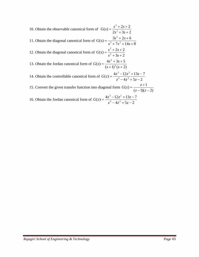
Rajagiri School of Engineering & Technology Page 45
10. Obtain the observable canonical form of 232
22)(
2
2
ss
sssG
11. Obtain the diagonal canonical form of 8147
623)(
23
2
sss
sssG
12. Obtain the diagonal canonical form of 23
22)(
2
2
ss
sssG
13. Obtain the Jordan canonical form of )2()1(
534)(
2
2
ss
sssG
14. Obtain the controllable canonical form of 254
713124)(
23
23
zzz
zzzzG
15. Convert the given transfer function into diagonal form )2)(1(
1)(
zz
zzG
16. Obtain the Jordan canonical form of 254
713124)(
23
23
zzz
zzzzG

Rajagiri School of Engineering & Technology Page 46
7.1 COURSE INFORMATION SHEET
PROGRAMME: Electrical and Electronics
Engineering
DEGREE: BTECH
COURSE: Digital Signal Processing SEMESTER: 6 CREDITS: 4
COURSE CODE: EE010604
REGULATION:UG
COURSE TYPE: Core
COURSE AREA/DOMAIN: : Electrical and
Electronics /Communication
CONTACT HOURS: 4(Lecture)+2 (Tutorial)
hours/Week.
CORRESPONDING LAB COURSE CODE (IF
ANY):NIL
LAB COURSE NAME:NIL
SYLLABUS:
UNIT DETAILS HOURS
I Discrete time signals and systems: Basic principles of signal processing-Building
blocks of digital signal processing. Review of sampling process and sampling
theorem. Standard signals-delta, step, ramp. Even and odd functions. Properties of
systems-linearity, causality, time variance, convolution and stability –difference
equations-frequency domain representation – Discrete – time Fourier transform and
its properties- Z transform and inverse Z transform-solution of difference equations.
12
II Discrete fourier transform-inverse discrete fourier transform-properties of DFT-linear
and circular convolution-overlap and add method-overlap and save method-FFT -
radix 2 DIT FFT-Radix2 DIF FFT
12
III Digital filter design: Design of IIR filters from analog filters - analog butter worth
functions for various filters - analog to digital transformation-backward difference
and forward difference approximations-impulse invariant transformation – bilinear
transformation frequency warping and pre warping-design examples- frequency
transformations. Structures for realizing digital IIR filters-Direct form 1-direct form
II-parallel and cascade structure -lattice structure.
17
IV Design of FIR filters-Properties of FIR filters-Design of FIR filters using fourier
series method- Design of FIR filters without using windows- Design of FIR filters
using windows- Design using frequency sampling-Design using frequency sampling
method-Design using Kaiser‟s approach- realization of FIR filters.
13
DIGITAL SIGNAL PROCESSING- EE 010 604

Rajagiri School of Engineering & Technology Page 47
V Finite register length problems in digital filters-fixed point and floating point formats-
errors due to quantization, truncation and round off. Introduction to DSP processors.
Architecture of TMS 320C54 XX Digital Signal Processor. Principle of speech signal
processing (Block Schematic only).
9
TOTAL HOURS 63
TEXT/REFERENCE BOOKS:
T/R BOOK TITLE/AUTHORS/PUBLICATION
T/R Signals and Systems ,Simon Haykin and Barry Van Veen , Second Edn,John Wiley,India ,2010.
T/R Digital Signal Processing ,John G. Proakis, Dimitris G. Manolakis, PHI,New Delhi,1997
T/R Digital Signal Processing, P.Ramesh Babu and R. Ananda Natarajan, , Second Edition
,SCITECH,2008
T/R Digital Signal Processing ,Mitra , Tata McGraw –Hill Education New Delhi,2007
T/R Digital Signal Processing,Ganesh Rao, Sanguins,2007
COURSE PRE-REQUISITES:
C.CODE COURSE NAME DESCRIPTION SEM
EE010 503 Signals and Sytems Basics of signals and systems 5
EN010301A Engineering Mathematics II Z transforms 3
EN010 401 Engineering Mathematics III Fourier series, Fourier Transform 4
COURSE OBJECTIVES:
1 To provide knowledge of transforms for the analysis of discrete time systems.
2 To impart knowledge in digital filter design techniques and associated problems.
COURSE OUTCOMES:
SNO DESCRIPTION BLOOM‟S
TAXONOMY
LEVEL
1 Students will be able to apply the knowledge of mathematics in discrete
time signals and systems
Comprehension
[Level 1]
2 Students will be able to compute and analyse discrete time Fourier
Transform ( DTFT), Discrete Fourier Transform (DFT) and Z transform
Knowledge
[Level 2]

Rajagiri School of Engineering & Technology Page 48
3 Students will be able to identify and demonstrate the design and realization
of Digital IIR Filters.
Analysis
[Level 4]
4 Students will be able to identify and f demonstrate the design and realization
of Digital FIR Filters.
Analysis
[Level 4]
5 Students will be able to recall the basic knowledge in the Digital Signal
Processors to solve complex problems and to manage projects in signal
processing
Application
[Level 3]
MAPPING COURSE OUTCOMES (COs) – PROGRAM OUTCOMES (POs) AND
COURSE OUTCOMES (COs) – PROGRAM SPECIFIC OUTCOMES (PSOs)
PO
1
PO
2
PO
3
PO
4
PO
5
PO
6
PO
7
PO
8
PO
9
PO
10
PO
11
PO
12
PSO1 PSO2 PSO3
EE010604.1 3 3 2 2 2 2 1
EE010604. 2 2 3 3 2 3 1 3 2 1 1
EE010604. 3 3 3 3 2 2 2 2 2 1 1
EE010604. 4 2 3 3 2 1 1 1 1 1 3 3 1 1 1
EE010604. 5 3 3 3 3 1 1 2 2 2 3 2 1
EE010604 3 3 3 2 2 2 1 1 1 2 2 2 2 2 1
JUSTIFATIONS FOR CO-PO MAPPING:
Mapping L/H/M Justification
EE010604.
1-PO1
H Student will be able to apply the knowledge of Engineering
fundamentals to write equations for in discrete time signals and
systems
EE010604.
1-PO2
H Student will be able to formulate and analyze the discrete time
signals
EE010604.
1-PO3
M Student will be able to able to explain the discrete time signal and
systems
EE010604.
1-PO4
M Student will be able to design and synthesis the systems based on
the basic research of signals and systems
EE010604. M Student will be able to able to recall Z transform, DFT and DTFT

Rajagiri School of Engineering & Technology Page 49
2-PO1
EE010604.
2-PO2
H Student will be able to able to select DTFT, DFT and Z transform
EE010604.
2-PO3
H Student will be able to able to select the solutions for DTFT, DFT
and Z transform
EE010604.
2-PO4
M Student will be able to able to recognize transform for a particular
signal
EE010604.
2-PO5
H Student will be able to able to select a required transform for a
signal
EE010604.
2-PO10
L Student will be able to able to list the discrete Fourier transforms
which is need to apply
EE010604.
2-PO11
M Student will be able to able to recall DTFT,DFT and Z transform
EE010604.
3-PO1
H Student will be able to explain the design and realization of Digital
IIR Filters.
EE010604.
3-PO2
H Student will be able to identify and formulate the design of
different types IIR filter
EE010604.
3-PO3
H Student will be able to choose and Design the IIR filters
transformatons like backward difference and forward difference
approximations-impulse invariant transformation – bilinear
transformation etc
EE010604.
3-PO4
M Student will be able to design and analyse the different
transformations for IIR filter
EE010604.
3-PO5
M Student will be able to apply the selection of IIR filter types
EE010604.
3-PO6
M Student will be able to show societal, health, safety using the
design of different IIR filter and its realization.
EE010604.
3-PO11
M Student will be able to perform the project using realization of IIR
filters
EE010604.
4-PO1
M Student will be able to analyse the fundamental knowledge of FIR
filters
EE010604.
4-PO2
H Student will be able to differentiate FIR design methods like
fourier series method, FIR filters using windows, frequency sampling
method, Kaiser‟s approach etc
EE010604.
4-PO3
H Student will be able to identify and design the FIR filters
EE010604.
4-PO4
M Student will be able to investigate the complex problems using
design methods like fourier series method, windows method, frequency

Rajagiri School of Engineering & Technology Page 50
sampling method, Kaiser‟s approach etc
EE010604.
4-PO5
L Student will be able to select, and apply appropriate techniques for
FIR filters
EE010604.
4-PO6
L Student will be able to conclude applications of FIR filters
EE010604.
4-PO7
L Student will be able to justify the use of FIR filter and it‟s
applications in sustainable development
EE010604.
4-PO9
L Student will be able to resolve the realization problems using FIR
filter realization methods
EE010604.
4-PO10
L Student will be able to contrast the effective communication using
realization of FIR filters
EE010604.
4-PO11
H Student will be able to criticize the filters and manage projects in
multi disciplinary environments
EE010604.
4-PO12
H Student will be able to justify the usage of the FIR filters and lead
to life- long learning
EE010604.
5-PO1
H Student will be able to show the selection of Digital Signal
Processors
EE010604.
5-PO2
H Student will be able to Predict, Identify, formulate and review the
Finite register length problems in digital filters
EE010604.
5-PO3
H Student will be able to choose the Digital Signal Processors and
various specialized digital applications by considering the public
health, safety, cultural, societal, and environmental considerations.
EE010604.
5-PO5
H Student will be able to demonstrate Digital signal processors like
TMS 320C54 XX
EE010604.
5-PO6
L Student will be able to choose the applications of Digital DSP
processors, which can be used for the society
EE010604.
5-PO8
L Student will be able to apply ethical principles and commit to
professional ethics and responsibilities and norms of the
Engineering practice using DSP processors applications
EE010604.
5-PO10
M Student will be able to write effective reports and design
documentation, make effective presentations, and give and receive
clear instructions.
EE010604.
5-PO11
M Student will be able to construct the circuits using digital
processors and manage projects in multi disciplinary
environments
EE010604.
5-PO12
M Student will be able to show the applications using DSP processors
and which leads to life- long learning

Rajagiri School of Engineering & Technology Page 51
GAPS IN THE SYLLABUS - TO MEET INDUSTRY/PROFESSION REQUIREMENTS:
SNO DESCRIPTION PROPOSED
ACTIONS
RELEVANCE
WITH POs
RELEVANCE
WITH PSOs
1 Students are not informed about solutions of digital
signal processing using software tools
MATLAB 1,2,3,4,5 1,2,3
PROPOSED ACTIONS: TOPICS BEYOND SYLLABUS/ASSIGNMENT/INDUSTRY VISIT/GUEST
LECTURER/NPTEL ETC
TOPICS BEYOND SYLLABUS/ADVANCED TOPICS/DESIGN:
SL
NO.
DESCRIPTION PROPOSED
ACTIONS
RELEVANCE
WITH Pos
RELEVANCE
WITH PSOs
1 Students are given basic
introduction to MATLAB
for solving digital signal
processing problems
Familiarisation of
MATLAB
1,2,3,4,5,6,7,
9,11,12
1,2,3
2 Students are introduced to
new DSP processors like
Micro Chip make DS PIC
Talk on DSPiC 1,2,3,4,5,6,7,9,11,12 1,2,3
WEB SOURCE REFERENCES:
1 Prof. Alan V. Oppenheim (2011, spring),Digital Signal Processing [ On line]. Available:
http://ocw.mit.edu/resources/res-6-008-digital-signal-processing-spring-2011/index.htm
2 Prof: Govind Sharma ( ) Digital Signal Processing [ On line] .Available :
http://nptel.iitm.ac.in/courses/Webcourse-contents/IIT-KANPUR/Digi_Sign_Pro/ui/TOC.htm
DELIVERY/INSTRUCTIONAL METHODOLOGIES:
CHALK & TALK STUD.
ASSIGNMENT
WEB RESOURCES
LCD/SMART
BOARDS
STUD. SEMINARS ADD-ON COURSES
ASSESSMENT METHODOLOGIES-DIRECT
ASSIGNMENTS STUD. SEMINARS TESTS/MODEL
EXAMS
UNIV.
EXAMINATION
STUD. LAB
PRACTICES
STUD. VIVA MINI/MAJOR
PROJECTS
CERTIFICATIONS

Rajagiri School of Engineering & Technology Page 52
ADD-ON COURSES OTHERS
ASSESSMENT METHODOLOGIES-INDIRECT
ASSESSMENT OF COURSE OUTCOMES (BY
FEEDBACK, ONCE)
STUDENT FEEDBACK ON FACULTY
(TWICE)
ASSESSMENT OF MINI/MAJOR PROJECTS BY
EXT. EXPERTS
OTHERS
Prepared by Approved by
Mr. Ginnes K John Ms. Santhi B
HOD
7.2 COURSE PLAN
L/T
Sr.
No.
Date
( year
2017)
Topics
Module I
L1 Jan 23 Discrete time signals and systems, Building blocks of digital signal processing
L2 Jan 24 sampling process and sampling theorem
L3 Jan 24 Standard signals-delta, step, ramp. Even and odd functions
T1 Jan 27 Tutorial for Lecture1 to Lecture 3
L4 Jan 30 Properties of systems-linearity, causality, time variance, convolution and stability
L5 Jan 31 Discrete – time Fourier transform , Discrete – time Fourier transform properties
L6 Jan 31 Z transform, Inverse Z transform
T2 Feb 2 Tutorial for Lecture5 to Lecture 6
L7 Feb 3 solution of difference equations
Module II starts
L8 Feb 6 Discrete Fourier transform, Inverse discrete Fourier transform
L9 Feb 7 properties of DFT
L10 Feb 7 Linear and circular convolution
T3 Feb 9 Tutorial for L8-L10
L11 Feb 10 Overlap and add method
L12 Feb 13 Overlap and save method
L13 Feb 14 FFT - radix 2 DIT
T4 Feb 14 Tutorial for L11-L13
L14 Feb 16 Radix2 DIT FFT
L15 Feb 17 Radix2 DIF FFT
Module III starts
L16 Feb 20 Design of IIR filters from analog filters, Analog butter worth functions for various
filters

Rajagiri School of Engineering & Technology Page 53
T5 Feb 21 Tutorial for L16
L17 Feb 21 Analog to digital transformation
L18 Feb 23 Backward difference and forward difference approximations
L19 Feb 27 Impulse invariant transformation
L20 Feb 28 Bilinear transformation
T6 Feb 28 Tutorial for L17 to L20
L21 March 2 Frequency warping and pre warping, Structures for realizing digital IIR filters-
Direct form 1
T7 March 6 Direct form II
L22 March 7 Structures for realizing digital IIR filters
T8 March 7 Parallel and cascade structure
T9 March 9 Lattice structure
Module IV starts
L23 March 16 Design of FIR filters - Fourier series method
L24 March 17 Properties of FIR filters, Design of FIR filters using windows
T10 March 20 Tutorial for L23 to L24
L25 March 21 Design of FIR filters using Rectangular window
L26 March 21 Design of FIR filters using Hamming window, Hanning windows
T11 March 23 Tutorial for Design of FIR filters using Hamming windows
T12 March 24 Tutorial for Design of FIR filters using Hanning windows
L27 March 27 Design using frequency sampling method
T13 March 28 Tutorial for L27
L28 March 28 Design using Kaiser‟s approach
T14 March 30 Tutorial for L28
L29 March 31 Realization of FIR filters
Module V starts
L30 April 3 Finite register length problems in digital filters
L31 April 4 Fixed point and floating point formats
T15 April 4 Tutorial for L30 to L31
L32 April 6 Errors due to quantization, truncation and round off
L33 April 7 Errors due to quantization, truncation and round off
T16 April 10 Tutorial session
L34 April l1 Introduction to DSP processors
L35 April 11 Architecture of TMS 320C54 XX Digital Signal Processor
L36 April 17 Architecture of TMS 320C54 XX Digital Signal Processor
L37 April 18 Principle of speech signal processing
T17 April 18 Tutorial session
T18 April 20 Problems – Review of all modules
T19 April 21 Problems – Review of all modules

Rajagiri School of Engineering & Technology Page 54
7.3 ASSIGNMENT
Assignment No: 1
1. Derive radix 2 DIF FFT algorithm
2. Derive radix 2 DIT FFT algorithm
Assignment No: 2
1. Give a brief introduction to DSP Processors
2. Discuss the architecture of TMS 320 C 54XX Digital signal processor
3. Explain the principle of speech signal processing.
4. Discuss the basics of errors due to quantization, truncation and round off
7.4 TUTORIAL
1. Determine inverse Z transform of 1 2
1( )
1 1.5 0.5X z
z z
for (i) ROC: 1z
(ii) ROC : 0.5z
(iii) ROC : 0.5 1z
2. Determine the response of FIR filter whose unit sample response is given as, ( ) 1, 2h n
when input applied is, ( ) 2,1x n .
(i) Use linear convolution.
(ii) Then find circular convolution so that response getting from circular convolution
is same as linear convolution.
3. Compute DFT of the following sequence using DIT-FFT algorithm.

Rajagiri School of Engineering & Technology Page 55
( ) 1,1,0,0, 1, 1,0, 0x n
4. A long sequence x(n) is filtered through a filter with impulse response h(n) to yield the output
y(n). If ( ) 1,4,3,0,7,4, 7, 7, 1,3,4,3x n , ( ) 1,2h n . Compute y(n) using overlap add
technique. Use only a 5 point circular convolution in your approach.
5. The system function of the analog filter is given as, 2
0.1( )
( 0.1) 9a
sH s
s
. Obtain the system
function of the IIR digital filter by using impulse invariant method.
6. Determine the filter coefficients hd(n) for the desired frequency response of a low pass filter
given by
2
4 4( )
04
j
j
d
e for
H e
for
If we define the new filter coefficients by h(n)= hd(n).w(n) , where
1 0 4
( )0
for nw n
elsewhere
Determine h(n)
7. Determine the impulse response h(n) of a filter having desired frequency response,
( 1) /2 02
( )
02
j N
j
d
e for
H e
N=7 , use frequency sampling approach.

Rajagiri School of Engineering & Technology Page 56
8.1 COURSE INFORMATION SHEET
PROGRAMME: Electrical & Electronics
Engineering
DEGREE: B.TECH
COURSE: MICROCONTROLLERS &
EMBEDDED SYSTEMS
SEMESTER: VI CREDITS: 4
COURSE CODE: EE010 605 REGULATION:
UG
COURSE TYPE: CORE
COURSE AREA/DOMAIN: Embedded
Systems
CONTACT HOURS: 3+1 (Tutorial) hours/Week.
CORRESPONDING LAB COURSE CODE (IF
ANY): Yes
LAB COURSE NAME: Microprocessor and
Microcontroller Lab
SYLLABUS:
UNIT DETAILS HOURS
I
Introduction to embedded systems (block diagram description)- microcontrollers and microprocessors – comparison. intel 8051: architecture–block diagram-oscillator and clock-internal registers-program counterpsw-register banks-input and output ports internal
and external memory, counters and timers, serial data i/o- interrupts
– sfrs
14
II
Programming of 8051: instruction syntax-types of instructions–
moving data-arithmetic instructions-jump and call instructions-logical
instructions-single bit
instructions. arithmetic programs timing subroutines –software time
delay- oftware polled timer addressing modes
application of keil c in microcontroller programming.
14
III
i/o programming: timer/counter programming-interrupts
programming- timer and external interrupts
serial communication- different character transmission techniques using
time delay, polling and interrupt driven-receiving serial data – polling
for received data, interrupt driven data reception-rs232 serial bus
standard.
10
MICRO CONTROLLER & EMBEDDED SYSTEMS- EE010 605

Rajagiri School of Engineering & Technology Page 57
IV
Microcontroller system design: external memory and memory address
decoding for eprom and ram. interfacing keyboard. 7 segment
display and lcd display.-interfacing of adc (0808) and dac (808) to
8051-frequency measurement - interfacing of stepper motor.
10
V
Introduction to risc microcontrollers: architecture of pic 16f877
microcontrollerfsr -different reset conditions.various oscillator
connections- internal rc, external rc, crystal oscillator and external
clock.pic
memory organization – program (code) memory and memory map,
data memory and data eeprom.instruction set – different addressing
modes. timers - interrupt structure in pic 16f877
microcontroller.simple assembly
language programs - square wave generation - reading/writing with
internal data eeprom.
12
TOTAL HOURS 60
TEXT/REFERENCE BOOKS:
T/R BOOK TITLE/AUTHORS/PUBLICATION
T MUHAMMAD ALI MAZIDI AND JANICE GILLISPIEMAZIDI, THE 8051
MICROCONTROLLER AND EMBEDDED SYSTEMS, PEARSON EDUCATION ASIA. T AJAY V DESHMUKH , MICROCONTROLLERS- THEORY AND APPLICATIONS , TATA
MCGRAW – HILL EDUCATION, NEW DELHI R KENNETH J.AYALA, THE 8051 MICROCONTROLLER – ARCHITECTURE,
PROGRAMMING AND APPLICATIONS, PENRAM INTERNATIONAL PUBLISHING
(INDIA),ED 2
R K.V.SHIBU, INTRODUCTION TO EMBEDDED SYSTEMS, 1E, TATA MCGRAW –
HILL EDUCATION, NEW DELHI 2009
R JOHN B. PEATMAN, DESIGN WITH PIC MICROCONTROLLERS , PEARSON
EDUCATION
R MYKEPREDKO, PROGRAMMING AND CUSTOMIZING THE 8051
MICROCONTROLLER, TATA MCGRAW HILL EDUCATION, NEW DELHI, 2009
R INTEL DATA BOOK ON MCS 51 FAMILY
COURSE PRE-REQUISITES:
C.CODE COURSE NAME DESCRIPTION SEM

Rajagiri School of Engineering & Technology Page 58
EE010506 MICROPROCESSORS &
APPLICATIONS
A THOROUGH UNDERSTANDING
ABOUT THE BASICS OF
MICROPROCESSORS, PROGRAMMING
AND APPLICATIONS.
5
COURSE OBJECTIVES:
1 To impart an insight into the architecture of 8051 microcontroller. 2 To develop sound understanding about programming and interfacing of 8051
microcontroller. 3 To develop understanding of advanced pic 16f877 microcontroller and embedded
systems.
COURSE OUTCOMES:
SNO DESCRIPTION Blooms’ Taxonomy Level
1 Students will be able to develop an idea about the
basics of embedded systems and of
microcontrollers.
Knowledge [Level 1]
2 Students will be able to program a microcontroller
system in assembly code and c.
Application [Level 3]
3 Students will be able to design and interface
microcontroller-based embedded systems.
Application [Level 3]
4 Students will be able to develop a basic knowledge
about pic 16f877.
Knowledge [Level 1]
5 Students will be able to develop a basic idea on
programming of pic 16f877.
Comprehension [Level 2]
MAPPING COURSE OUTCOMES (COs) – PROGRAM OUTCOMES (POs) AND COURSE OUTCOMES (COs) –
PROGRAM SPECIFIC OUTCOMES (PSOs)
PO 1 PO 2 PO 3 PO 4 PO 5 PO 6 PO 7 PO 8 PO 9 PO 10 PO 11 PO 12 PSO 1 PSO 2 PSO 3
C 605.1 2 2 1 1 1 1 1 1 2 1 1
C 605. 2 2 2 2 1 1 2 2 2 1 1
C 605. 3 2 2 2 1 1 2 2 2 1 1
C 605. 4 2 2 1 1 1 1 1 1 2 1 1
C 605. 5 2 2 1 1 1 1 1 1 2 1 1
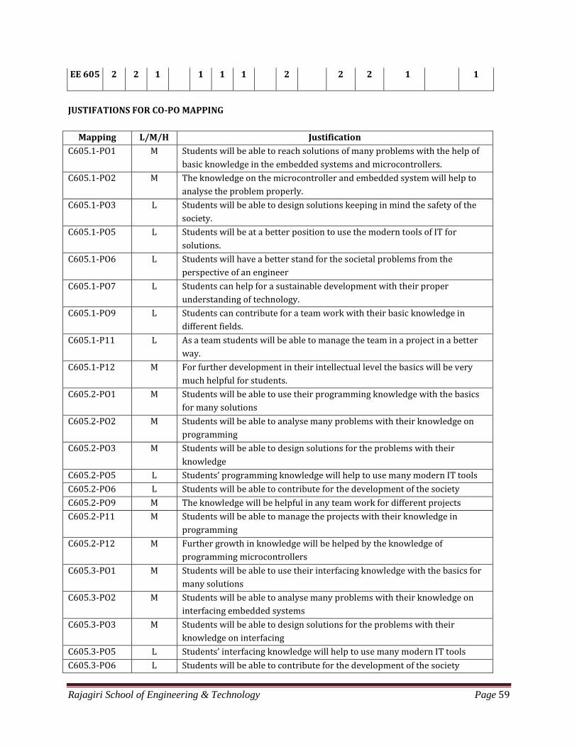
Rajagiri School of Engineering & Technology Page 59
EE 605 2 2 1 1 1 1 2 2 2 1 1
JUSTIFATIONS FOR CO-PO MAPPING
Mapping L/M/H Justification
C605.1-PO1 M Students will be able to reach solutions of many problems with the help of
basic knowledge in the embedded systems and microcontrollers.
C605.1-PO2 M The knowledge on the microcontroller and embedded system will help to
analyse the problem properly.
C605.1-PO3 L Students will be able to design solutions keeping in mind the safety of the
society.
C605.1-PO5 L Students will be at a better position to use the modern tools of IT for
solutions.
C605.1-PO6 L Students will have a better stand for the societal problems from the
perspective of an engineer
C605.1-PO7 L Students can help for a sustainable development with their proper
understanding of technology.
C605.1-PO9 L Students can contribute for a team work with their basic knowledge in
different fields.
C605.1-P11 L As a team students will be able to manage the team in a project in a better
way.
C605.1-P12 M For further development in their intellectual level the basics will be very
much helpful for students.
C605.2-PO1 M Students will be able to use their programming knowledge with the basics
for many solutions
C605.2-PO2 M Students will be able to analyse many problems with their knowledge on
programming
C605.2-PO3 M Students will be able to design solutions for the problems with their
knowledge
C605.2-PO5 L Students’ programming knowledge will help to use many modern IT tools
C605.2-PO6 L Students will be able to contribute for the development of the society
C605.2-PO9 M The knowledge will be helpful in any team work for different projects
C605.2-P11 M Students will be able to manage the projects with their knowledge in
programming
C605.2-P12 M Further growth in knowledge will be helped by the knowledge of
programming microcontrollers
C605.3-PO1 M Students will be able to use their interfacing knowledge with the basics for
many solutions
C605.3-PO2 M Students will be able to analyse many problems with their knowledge on
interfacing embedded systems
C605.3-PO3 M Students will be able to design solutions for the problems with their
knowledge on interfacing
C605.3-PO5 L Students’ interfacing knowledge will help to use many modern IT tools
C605.3-PO6 L Students will be able to contribute for the development of the society

Rajagiri School of Engineering & Technology Page 60
C605.3-PO9 M The knowledge will be helpful in any team work for different projects
C605.3-P11 M Students will be able to manage the projects with their knowledge in
interfacing embedded systems
C605.3-P12 M Further growth in knowledge will be helped by the knowledge of
interfacing embedded systems.
C605.4-PO1 M Students will be able to reach solutions of many problems with the help of
basic knowledge on PIC 16F877.
C605.4-PO2 M The knowledge on PIC 16F877 will help to analyse the problem properly.
C605.4-PO3 L Students will be able to design solutions keeping in mind the safety of the
society.
C605.4-PO5 L Students will be at a better position to use the modern tools of IT for
solutions.
C605.4-PO6 L Students will have a better stand for the societal problems from the
perspective of an engineer
C605.4-PO7 L Students can help for a sustainable development with their proper
understanding of technology.
C605.4-PO9 L Students can contribute for a team work with their basic knowledge in
different fields.
C605.4-P11 L As a team students will be able to manage the team in a project in a better
way.
C605.4-P12 M For further development in their intellectual level the basics will be very
much helpful for students.
C605.5-PO1 M Students will be able to reach solutions of many problems with the help of
basic knowledge on PIC 16F877.
C605.5-PO2 M The knowledge on PIC 16F877 will help to analyse the problem properly.
C605.5-PO3 L Students will be able to design solutions keeping in mind the safety of the
society.
C605.5-PO5 L Students will be at a better position to use the modern tools of IT for
solutions.
C605.5-PO6 L Students will have a better stand for the societal problems from the
perspective of an engineer
C605.5-PO7 L Students can help for a sustainable development with their proper
understanding of technology.
C605.5-PO9 L Students can contribute for a team work with their basic knowledge in
different fields.
C605.5-P11 L As a team students will be able to manage the team in a project in a better
way.
C605.5-P12 M For further development in their intellectual level the basics will be very
much helpful for students.
GAPS IN THE SYLLABUS - TO MEET INDUSTRY/PROFESSION REQUIREMENTS:
SNO DESCRIPTION PROPOSED
ACTIONS
RELEVANCE
WITH POs
RELEVANCE
WITH PSOs
1. PROGRAMMING USING VARIOUS 3,5,9,11 1,3

Rajagiri School of Engineering & Technology Page 61
SIMULATION SOFTWARE
MULTISIM.
PROGRAMMING
EXAMPLES
USING
MULTISIM.
PROPOSED ACTIONS: TOPICS BEYOND SYLLABUS/ASSIGNMENT/INDUSTRY VISIT/GUEST
LECTURER/NPTEL ETC
TOPICS BEYOND SYLLABUS/ADVANCED TOPICS/DESIGN:
SNO DESCRIPTION PROPOSED
ACTIONS
RELEVANCE
WITH POs
RELEVANCE
WITH PSOs
1 KEIL C PROGRAMMING FOR TIMERS,
INTERRUPTS & SERIAL
COMMUNICATION.
Extra
Classes to
introduce
the same
3,5,9,11 1,3
2 INTERFACING OF 8255 PPI TO 8051
MICROCONTROLLER.
Extra
Classes to
introduce
the same
3,5,9,11 1,3
WEB SOURCE REFERENCES:
1 MICROCHIP, “28/40-PIN 8-BIT CMOS FLASH MICROCONTROLLERS,”
DS30292C DATASHEET, 2001.
DELIVERY/INSTRUCTIONAL METHODOLOGIES:
CHALK & TALK STUD. ASSIGNMENT WEB RESOURCES
LCD/SMART
BOARDS
STUD. SEMINARS ADD-ON COURSES
ASSESSMENT METHODOLOGIES-DIRECT
ASSIGNMENTS STUD. SEMINARS TESTS/MODEL
EXAMS
UNIV. EXAMINATION
STUD. LAB
PRACTICES
STUD. VIVA MINI/MAJOR
PROJECTS
CERTIFICATIONS
ADD-ON COURSES OTHERS

Rajagiri School of Engineering & Technology Page 62
ASSESSMENT METHODOLOGIES-INDIRECT
ASSESSMENT OF COURSE OUTCOMES (BY
FEEDBACK, ONCE)
STUDENT FEEDBACK ON FACULTY (TWICE)
ASSESSMENT OF MINI/MAJOR PROJECTS BY
EXT. EXPERTS
OTHERS
Prepared by Approved by
Fr. Mejo Gracevilla CMI Ms. Santhi B
HOD EEE
8.2 COURSE PLAN
Sl
No Module Date Planned
1
1
16-Jan-17 Introduction to Embedded Systems
2 17-Jan-17 Introduction to Microcontrollers and Comparison between
Microprocessors and Microcontrollers
3 18-Jan-17 Intel 8051: Architecture–Block diagram
4 19-Jan-17 Oscillator and Clock-Internal Registers-Program Counter &
DPTR
5 23-Jan-17 PSW-Register Banks- SFRs-Stack & Stack Pointer
6 24-Jan-17 Internal Memory Organisation
7 25-Jan-17 External Memory Organisation
8 30-Jan-17 Timer & Counter
9 31-Jan-17 Serial data Communication
10 1-Feb-17 Interrupts
11 2-Feb-17 Input and Output ports
12
2
6-Jan-17 Programming of 8051: Instruction syntax- Addressing Modes
(contd...)
13 7-Feb-17 Addressing Modes
14 8-Feb-17 Types of instructions–Moving data
15 9-Feb-17 Arithmetic Instructions
16 9-Feb-17 Jump & Call Instructions

Rajagiri School of Engineering & Technology Page 63
17 13-Feb-17 Logical Instructions
18 14-Feb-17 Push ,Pop & Exchange Opcodes
19 15-Feb-17 Introduction to Arithmetic Programs (contd..)
20 16-Feb-17 Programming Tutorials
21 20-Feb-17 Application of Keil C in microcontroller programming
22 21-Feb-17 Programming Tutorials
23
3
22-Feb-17 I/O Programming: Timing subroutines –Software time delay
24 23-Feb-17 Software polled timer- Timer/Counter Programming modes
(contd...)
25 27-Feb-17 Timer/Counter Programming modes
26 28-Feb-17 Tutorials on Timer/Counter Programming
27 1-Mar-17 Interrupts Programming
28 2-Mar-17 Tutorials on Interrupts Programming
29 6-Mar-17 Timer Interrupts & External Interrupts
30 7-Mar-17 Introduction to Serial Communication-Modes of serial
communication
31 8-Mar-17 RS232 Serial Bus standard-MAX232
32 9-Mar-17 Character transmission techniques using interrupts,time delay
and polling
33 15-Mar-17 Receiving serial data--Polling for received data and interrupt
driven data receptio
34
4
16-Mar-17 Microcontroller system design: External memory and
Memory Address Decoding for EPROM and RAM.
35 21-Mar-17 Interfacing keyboard
36 22-Mar-17 Interfacing 7 segment display
37 23-Mar-17 Interfacing LCD display
38 24-Mar-17 Interfacing of ADC (0808)
39 27-Mar-17 Interfacing of DAC (0808) to 8051
40 28-Mar-17 Frequency measurement

Rajagiri School of Engineering & Technology Page 64
41 29-Mar-17 Interfacing of stepper motor
42
5
30-Mar-17 Introduction to RISC Microcontrollers: Architecture of PIC
16F877 microcontroller
43 3-Apr-17 FSR– different Reset conditions -Various oscillator
connections
44 4-Apr-17 PIC memory organization
45 5-Apr-17 Program (Code) memory and memory map
46 6-Apr-17
Data memory and Data EEPROM--Interrupt structure in PIC
16F877 microcontroller --Instruction set – Different
addressing modes
47 10-Apr-17 Brief description of Ports,CCP module,Serial
communication,ADC and Timers
48 11-Apr-17 Tutorials on square wave generation and reading with
internal data EEPROM
49 12-Apr-17 Tutorials on writing with internal data EEPROM
50 17-Apr-17 Tutorials
51 18-Apr-17 Tutorials

Rajagiri School of Engineering & Technology Page 65
8.3 ASSIGNMENT
Assignment 1
1. Briefly explain software polled timer.
2. Explain in detail (a) RS232 serial bus standard (b) MAX 32
Assignment 2
1. Explain (a) different reset conditions (b) various oscillator connections I PIC 16F877
2. Explain briefly about Timers in PIC 16F877
8.4 TUTORIAL
1. Write a program to add two 8 bit numbers stored in Port 0 and Port 1. Send the result to Port
2 and carry to Port 3.1.
2. Write a program to subtract two 8 bit numbers stored in Port 0 and Port 1. Send the result to
Port 2 and carry to Port 3.0.
3. Write a program to get the value of x from P1 and send x2
to P2 continuously.
4. Write a program to swap the nibbles of R0 and R1 so that low nibble of R0 swaps with high
nibble of R1 and high nobble of R0 with low nibble of R1.
5. You have five numbers stored in locations 40H to 44H. Check of any value equals 65H. If
yes, copy its location to R4, else make R4=0.
6. Assume 5 BCD numbers are stores in locations starting from 40H. Write a program to find
the sum of all the numbers. Result should be in BCD and store in register R7 9MSB) and
R6 (LSB).
Tutorial 2
1. Write a program to copy the value 55H into RAM locations 40H to 45H using (a) direct
addressing mode (b) register indirect addressing mode without a loop and (c) with a loop
2. For an 8051 system, with a crystal frequency of 11.0592 MHz, write a program to generate a
square wave on pin P1.0 with a duty cycle of 50%.
3. You have got the marks of 6 subjects out of 25d (19H). They are stored in locations starting
from 40H onwards. Find the average of your marks and store the result at 50H.
4. Write a program to convert a hexadecimal number to a decimal number
5. Write a program to read the temperature and test it for the value 75. According to the test
results, place the temperature value into the register indicated.
6. Ten hex numbers are stored in RAM locations 50H onwards. Write a program to find the
biggest number in the set. Save the biggest number in the location 60H.

Rajagiri School of Engineering & Technology Page 66
Tutorial 3
1. Write an 8051 C program to send values 00-FF to port P1.
2. Write an 8051 C program to monitor bit P1.5. If it is high, send 55H to P0, otherwise send
AAH to P2.
3. Write an 8051 C program to get a byte of data from P0. If it is less than 100, send it to P1,
otherwise send it to P2.
4. Write an 8051 C program to toggle all the bits of P1 continuously.
5. Write an 8051 C program to toggle bits of P1 ports continuously with a 250 ms delay.
Tutorial 4
1. WAP to create a square wave of 50% duty cycle on the P1.5 bit. Use Timer 0 to generatethe
timedelay.
2. Assume XTAL = 11.0592 MHz, WAP to generate a square wave of 50 Hz frequency on pin
P2.3
3. Generate a square wave with on time of 3ms and off time of 10ms on P1.0. Assume an
XTAL of22MHz.
4. Assume XTAL = 11.0592 MHz. WAP to generate a square of time period 4 sec on
P2.4.Use Timer1 in mode 1.
5. Write an 8051 C program to generate a square wave with 50% duty cycle on P1.5. Use
Timer 0,16-bit mode to generate the delay.
Tutorial 5
1. Assume XTAL = 11.0592 MHz. WAP to generate a square
wave with a frequency of 1835 Hz on pin P1.0.Use Timer 1 in mode 2.
2. Assume XTAL = 22 MHz, WAP to generate a square
wave of frequency 1kHz on pin P1.6. Use Timer 1 in mode 2.
3. Design a counter for counting no. of pulses of an input signal for 1sec and display the
count at Port2(LSB) & Port 1(MSB). The pulses are to be fed to pin P3.4.Use XTAL=22
MHz.
4. Assume that a 1-Hz external clock is being fed into pin T1 (P3.5).Write a Cprogram for
counter 1in mode 2 (8-bit auto reload) to count up and display the state of the TL1 count
on P1. Start thecount at 0H.
Tutorial 6
1. Write a program for the 8051 to transfer letter “A” serially at 4800 baud, continuously.
2. Write a program for the 8051 to transfer “YES” serially at 9600 baud, 8-bit data, 1 stop
bit, do thiscontinuously.
3. Write a program for the 8051 to receive bytes of data serially, and put them in P1, set the
baud rateat 4800, 8-bit data, and 1 stop bit.
4. Write a program for the 8051 to transfer letter “YES” serially at 4800 baud, continuously
usingdelay loop.

Rajagiri School of Engineering & Technology Page 67
5. Port 0 of 8051 is used to monitor a parameter in an industrial environment. If the
parameter givesa reading above 0FH,a message „High‟ should be sent serially.Otherwise
send a message „Okay‟serially. The words „High‟ & „Okay‟ are burnt into Program ROM
locations 0090H & 00A0Hrespectively.
Tutorial 7
1. WAP that displays a value of „Y‟ at P0 and „N‟ at P2 and also generate a square wave of
10kHz atpin P1.2 using Timer 0 in mode 2 with XTAL=22MHz.
2. WAP to generate 2 square waves –one of frequency 5kHz at pin P1.3 and another
frequency 25kHzat pin P2.3.Assume XTAL=22MHz.
3. Assume that the INT1 pin is connected to a switch that is normallyhigh. Whenever it goes
low, it should turn on an LED. The LED isconnected to P1.3 and is normally off. When it
is turned on it shouldstay on for a fraction of a second.
4. Write a program using interrupts to do the following:
(a) Receive data serially and sent it to P0,
(b) Read port P1 , transmit data serially, and give a copy to P2,
(c) Make timer 0 generate a square wave of 5kHz frequency on P3.7.
Assume that XTAL=11.0592 MHz. Set the baud rate at 4800.
Tutorial 8
1. Write a C program that continuously gets a single bit of data from P1.7and sends it to
P1.0, while simultaneously creating a square wave of200 μs period on pin P2.5. Use
Timer 0 to create the square wave.Assume that XTAL = 11.0592 MHz.
2. WAP to convert a hexadecimal number to a ASCII number.
3. Write a program to read 200 bytes of data from P1 and save the data inexternal RAM
starting atRAM location 5000H.
4. WAP to access a byte of data which is in data ROM(0000H), divide it by 2and save
quotient indata RAM(8000H).
5. Rewrite the above program if the data byte is in program ROM(100H).
Tutorial 9
1. A word „PPT‟ has been burned in the external data ROM locations startingfrom 4100H
onwards.WAP to copy this data into the internal data RAM locations of 8031 starting
from 60H onwards.
2. WAP to configure 8051 in Serial communication Mode 0. Send the data values stored in
locations700H to 70BH through serial port to an external device.
3. Write a 8051 C pgm
(a) to store ASCII letters A to E in ext. RAM addresses starting at 0
(b) getthe same data from external RAM and send it to P1 one byte at a time.
4. WAP to generate a square wave using PIC 16F877.

Rajagiri School of Engineering & Technology Page 68
5. WAP to read data from EEPROM data memory of PIC 16F877.
9.1 COURSE INFORMATION SHEET
PROGRAMME: Electrical and Electronics Engineering DEGREE: BTech COURSE: Renewable Energy Resources SEMESTER: VI CREDITS: 4 COURSE CODE: EE010 606 L06 REGULATION: UG COURSE TYPE: Elective COURSE AREA/DOMAIN: Electrical and Electronics Engineering
CONTACT HOURS: 2 (Lecture)+2 (Tutorial) hours/week
CORRESPONDING LAB COURSE CODE (IF ANY): Nil LAB COURSE NAME: Nil SYLLABUS: UNIT DETAILS HOURS
I
Energy Scenario in India, Environmental aspects in electrical energy generation, Energy for sustainable development, Renewable energy sources – Advantages and Limitations Renewable Hydro, Power equation, Small , Mini, Micro Hydro power, Types of turbines and generators
10
II
Solar energy – Introduction to solar energy, Solar radiation, availability, measurement and estimation Solar thermal systems – solar collectors (fundamentals only), Applications, Solar heating systems, Air conditioning and refrigeration system, Pumping system, Solar cooker, Solar Furnace, Solar Greenhouse, Design of solar water heater
11
III Solar photovoltaic systems, Photovoltaic conversion, Solar cell, module, panel and array, Solar cell- Materials - characteristics, efficiency, Battery back up - PV system classification, Design of standalone PV system
11
IV
Wind Energy – Introduction- Basic principles of wind energy extraction, wind data and energy estimation, site selection, Basic components of wind energy conversion system, Modes of wind power generation, Applications Fuel cells, characteristics, types and applications
13
V
Biomass Energy- Resources- Biofuels-Biomass conversion process-applications Tidal power – Energy estimation – site selection – Types – Important components of tidal power plants Wave energy – Characteristics, Energy and power from the waves, wave energy conversion devices Geothermal energy – resources – estimation of geothermal power- Geothermal energy conversion-Applications
15
TOTAL HOURS 60
RENEWABLE ENERGY RESOURSES -EE 010 606 L06

Rajagiri School of Engineering & Technology Page 69
TEXT/REFERENCE BOOKS: T/R BOOK TITLE/AUTHORS/PUBLICATION T D.P. Kothari, K.C. Singal, Rakesh Ranjan, Renewable Energy Sources and Emerging
Technologies, Prentice Hall of India, New Delhi, 2009 T B.H. Khan, Non-Conventional Energy Resources, 2nd Edition, Tata Mc GrawHill, New Delhi,
2010 T Chetan Singh Solanki, Renewable Energy Technologies, Prentice Hall of India, New Delhi, 2009 R Godfrey Boyle, Renewable Energy, Oxford University Press, 2004 R Tasneem Abbasi, S.A. Abbasi, Renewable Energy Sources, Prentice Hall of India, New Delhi,
2010 R Siraj Ahmed, Wind Energy – Theory and Practice , Prentice Hall of India, New Delhi 2010 COURSE PRE-REQUISITES: C.CODE COURSE NAME DESCRIPTION SEM EN 010 108 Basic Electrical Engineering Fundamentals of Electric Power
Generation 1 & 2
EN 010 107 Basic Mechanical Engineering Basics of Water Turbines 1 & 2 EE 010 306(ME)
Mechanical Technology Basics of Refrigeration & Air Conditioning
3
COURSE OBJECTIVES: 1 To understand the importance, scope and potential of Renewable Energy Resources 2 To impart knowledge on the theory and applications of Renewable Energy COURSE OUTCOMES: SNO DESCRIPTION BLOOMS’
TAXONOMY LEVEL
1 Graduates will be able to recognize the energy scenario and necessity of sustainable development utilising Renewable Energy recourses.
Knowledge Level 1
2 Graduates will be able to analyse and infer the potentials and design systems based on solar thermal applications.
Analyze Level 4
3 Graduates will be able to illustrate, design and implement stand alone solar photovoltaic systems.
Apply Level 3
4 Graduates will be able to understand the fundamentals and interpret basic components of wind energy extraction unit and predict its environmental impacts.
Understand Level 2
5 Graduates shall acquire knowledge on the applications of Renewable Energy Sources for producing Electrical Energy
Knowledge Level 1
MAPPING COURSE OUTCOMES (COs) – PROGRAM OUTCOMES (POs) AND COURSE OUTCOMES
(COs) – PROGRAM SPECIFIC OUTCOMES (PSOs):
PO 1 PO 2 PO 3 PO 4 PO 5 PO 6 PO 7 PO 8 PO 9 PO 10 PO 11 PO 12 PSO 1 PSO 2 PSO 3
C606.1 2 1 1 3 1 1
C606.2 2 3 1 2

Rajagiri School of Engineering & Technology Page 70
C606.3 1 2 1 1 2 1
C606.4 2 1 1 1
C606.5 1 1 1 1
EE 606 L06
JUSTIFATIONS FOR CO-PO MAPPING:
Mapping L/H/M Justification
C606.1-PO1 M Students will be able to explain and identify the energy scenario world
wide
C606.1-PO2 L Students will be able to formulate necessity of sustainable development
utilizing Renewable Energy recourses
C606.1-PO6 L Students will be able to identify renewable energy sources and suggest the
apt one for the society
C606.1-PO7 H Students will be able to understand the importance of Renewable energy for sustainable
development
C606.1-P12 M Students will be able to learn continoulsy from the fast changing technological nature of
renewable resources
C606.2-PO2 M Students will be able to identify systems based on solar thermal effects to meet the needs
of the end user
C606.2-PO3 H Students will be able to develop Solar thermal systems to meet the specific societal needs
C606.2-PO4 L Students will be able to analyze and interpret data from the area of Solar thermal
application.
C606.3-PO1 M Students will be able to analyse the problems persisting in the area of SPV systems
suggest long term sustainable solutions.
C606.3-PO3 M Students will be able to design and develop SPV systems to meet the specific societal
needs
C606.3-PO5 L Students will be able to apply modern tools to predict and analyse the advantages and
limitations of SPV systems
C606.3-PO11 L Students will be able to demonstrate the need for hybrid SPV for sustainable
development
C606.4-PO1 M Students will be able to apply the knowledge of basic wind energy systems and
communicate effectievly with public its need for societal development
C606.4-PO4 L Students will be able to research, analyse and interpret data in the area of wind energy
extraction.
C606.4-PO7 L Students will be able to apply the knowledge of wing energy extraction for the betterment
and sustainable growth of society
C606.5-PO1 L Students will be able to apply the knowledge of renewable energy resources to suggest
solution of energy crisis in human lives
C606.5-PO6 L Students will be able to learn continoulsy from the fast changing technological nature of
renewable resources
C606.5-PO7 L
Studnets will be able to understand issues related to conventional form of electricity
generation and demonstrate their knowledge and skill in power generation usinrg
renewable energy resources for sustainability

Rajagiri School of Engineering & Technology Page 71
GAPS IN THE SYLLABUS - TO MEET INDUSTRY/PROFESSION REQUIREMENTS: SNO DESCRIPTION PROPOSED
ACTIONS 1 The energy scenario statistics are not up to date Students are provided with the
latest statistics 2 Details regarding the existing renewable energy
installations are not present in the syllabus Details are provided by using power point slides
PROPOSED ACTIONS: TOPICS BEYOND SYLLABUS/ASSIGNMENT/INDUSTRY VISIT/GUEST LECTURER/NPTEL ETC TOPICS BEYOND SYLLABUS/ADVANCED TOPICS/DESIGN: 1 Information regarding the latest trends in the Renewable Energy Industry was imparted to
the students 2 Student groups were formed and asked to design posters related to some topics relevant to
the course WEB SOURCE REFERENCES: 1 (2017) MNRE Website [Online] Available: http://www.mnre.gov.in 2 (2017) ANERT Website [Online] Available: http://anert.gov.in/ DELIVERY/INSTRUCTIONAL METHODOLOGIES: CHALK & TALK STUD.
ASSIGNMENT WEB RESOURCES
LCD/SMART BOARDS
STUD. SEMINARS ADD-ON COURSES
ASSESSMENT METHODOLOGIES-DIRECT ASSIGNMENTS STUD. SEMINARS TESTS/MODEL
EXAMS UNIV. EXAMINATION
STUD. LAB PRACTICES
STUD. VIVA MINI/MAJOR PROJECTS
CERTIFICATIONS
ADD-ON COURSES OTHERS
ASSESSMENT METHODOLOGIES-INDIRECT ASSESSMENT OF COURSE OUTCOMES (BY FEEDBACK, ONCE)
STUDENT FEEDBACK ON FACULTY (TWICE)
ASSESSMENT OF MINI/MAJOR PROJECTS BY EXT. EXPERTS
OTHERS
Prepared by Approved by
Mr. Jebin Francis Ms. Santhi B 03/01/2017 HOD

Rajagiri School of Engineering & Technology Page 72
9.2 COURSE PLAN
Sl.No Module Planned Date Planned
1 1 30-Jan-2017 Energy scenario in India
2 1 31-Jan-2017 Environmental aspects of Electrical Energy Generation
3 1 1-Feb-2017 Environmental aspects of Electrical Energy Generation
4 1 3-Feb-2017 Energy for sustainable development,
5 1 6-Feb-2017 Renewable Energy sources-Advantages and limitations
6 1 7-Feb-2017 Renewable Hydro –Power Equation
7 1 8-Feb-2017 Small, Mini and Micro hydro power plant
8 1 10-Feb-2017 Small, Mini and Micro hydro power plant
9 1 13-Feb-2017 Types of turbines and generators used in SHP
10 1 14-Feb-2017 Types of turbines and generators used in SHP
11 1 15-Feb-2017 Types of turbines and generators used in SHP
12 1 17-Feb-2017 Types of turbines and generators used in SHP
13 2 20-Feb-2017 Solar energy – Introduction to solar energy
14 2 21-Feb-2017 solar radiation, availability, measurement and estimation.
15 2 22-Feb-2017 solar radiation, availability, measurement and estimation.
16 2 24-Feb-2017 solar radiation, availability, measurement and estimation.
17 2 27-Feb-2017 Solar Thermal systems- Solar collectors
18 2 28-Feb-2017 Applications -Solar heating system, Air conditioning and Refrigeration system
19 2 1-Mar-2017 Applications -Solar heating system, Air conditioning and Refrigeration system
20 2 3-Mar-2017 Pumping system, solar cooker, Solar Furnace, Solar Greenhouse
21 2 3-Mar-2017 Pumping system, solar cooker, Solar Furnace, Solar Greenhouse
22 2 6-Mar-2017 Design of solar water heater
23 2 7-Mar-2017 Design of solar water heater
24 3 17-Mar-2017 Solar photo voltaic systems -
25 3 20-Mar-2017 Photovoltaic conversion- Solar Cell, module, Panel and Array Solar cell-
26 3 21-Mar-2017 Photovoltaic conversion- Solar Cell, module, Panel and ArraySolar cell-
27 3 22-Mar-2017 Solar cell- materials-characteristics- efficiency-Battery back up-
28 3 24-Mar-2017 PV system classification
29 3 27-Mar-2017 Design of stand-alone PV system.

Rajagiri School of Engineering & Technology Page 73
30 3 27-Mar-2017 Design of stand-alone PV system.
31 4 28-Mar-2017 Wind energy –-Introduction
32 4 1-Apr-2017 Basic principles of wind energy extraction
33 4 3-Apr-2017 wind data and energy estimation
34 4 5-Apr-2017 site selection – Basic components of wind energy conversion system
35 4 6-Apr-2017 site selection – Basic components of wind energy conversion system
36 4 7-Apr-2017 Modes of wind power generation.
37 4 10-Apr-2017 Modes of wind power generation.
38 4 10-Apr-2017 tutorial
39 4 11-Apr-2017 Applications Fuel cells –characteristics-types and applications
40 4 11-Apr-2017 Applications Fuel cells –characteristics-types and applications
41 5 12-Apr-2017 Biomass Energy - Resources
42 5 13-Apr-2017 Biofuels- Biomass conversion process-applications
43 5 14-Apr-2017 Tidal power-Energy estimation
44 5 15-Apr-2017 site selection-Types-Important components of a tidal power plants
45 5 16-Apr-2017 Wave energy- characteristics-energy and power from the waves,
46 5 17-Apr-2017 Wave energy- characteristics-energy and power from the waves,
47 5 18-Apr-2017 Geothermal energy – resources - estimation of geothermal power
48 5 19-Apr-2017 geo thermal energy conversion – Applications
49 5 20-Apr-2017 geo thermal energy conversion – Applications

Rajagiri School of Engineering & Technology Page 74
9.3 ASSIGNMENT
Max. Marks : 10
Guidelines
1. Students are free to form groups (4 in a team)
2. Each team should do a Seminar and a Poster Presentation
3. Time duration: Seminar - 15 Mins + poster - 5 Mins
4. Topic – Emerging trends in Renewable Energy Recourses
a. Case Study
b. Processing Techniques
c. Design of standalone system
d. Renewable Energy Recourses in India/ world wide
e. Renewable Energy Systems in India/ world wide
9.4 TUTORIAL QUESTIONS
1. Evaluate the monthly average clearness index for 16 March 2017. at a surface located latitude 300 N. The monthly average daily terrestrial radiation on a horizontal surface is 28.1 MJ/m2/day.
2. Find the day-length in hours at New Delhi (28° 35’ N. 770 12’ E) on July 1 for a south facing surface tilted at 10°.
3. For the data of Question no. 2. find the local apparent time corresponding to 14:30 1ST. with correction of time as -4 minutes. if 1ST is based on 82° 30’ E.
4. Find the hour angle at the sunrise and the sunset for a horizontal surface with zenith angle or 90°. Ø = 20° and δ= —160.
5. find the hour angle at (the sunrise and the sunset on March 22 for a surface inclined at an angle 20° facing south at New Delhi (28° 35’ N, 770 12’ E).
6. Find the angle subtended by beam radiation with the normal to a flat-plate collector at 9 a.m. for the day on 30th October. 2003. The collector is placed at Mumbai (190 7’ N. 72° 51’ E), inclined at an angle 36 and is facing south.

Rajagiri School of Engineering & Technology Page 75
7. Compute the monthly average hourly solar flux received on 15th October on a flat -plate collector facing south having slope of 15°. The collector is located at chennai (13°.00 N).
a. The data given is: Time : 1-12 h (local apparent time) Ig = 2408 kJ/m2.h Id = 1073 kJ/m2. h The ground reflectivity is 0.2.
8. Compute the monthly average hourly solar flux received on a flat-plate collector facing due south (y = 00) having a slope or 120. The collector is located at a place 150 00’ N on 20th day of October. The data given are:
a. Time 11: 12 h (local apparent time) Hg = 2408 kJ/m2/h Hd = 1073 kJ/m2/h Ground reflectivity. p = 0.25. w = 7.50
9. Design a PV system for pumping 25000 litres of water every day from a depth of about 10m
10. Estimate the monthly average of daily global radiation on a horizontal surface at baroda (22°00’N, 73°l0’E) during the month of March 16th if the average sun shine hours per day is 9.5(a = 0.28 & b = 0.48).
11. A house uses 4 bulbs each of 40 W (8 hours a day ), 1 fan of 200 W (12 hours a day ) and an electric heater 1500W (1 hour a day).The house is to be electrified with solar panels . Calculate the current monthly bill for that house and also estimate the number of solar panels required for electrification.
12. A house owner decides to use solar PV system to run 2 CFLs (14 watt each) and 1 fan (60 watt) for 6 hours per day .What is the total load? Which PV module and battery is available for use? What would be the total cost of the system?
13. For a parabolic collector of length 2m, the angle of acceptance is 15ᵒ.Find the concentration ratio of the collector.
14. Wind speed is 10m/s at the standard atmospheric pressure. calculate (i)the total power density in the wind stream (ii)the total power produced by the turbine of 100 m diameter with an efficiency of 40%.Air density = 1.226 J/kg.K/m2.
15. Wind at one standard atmospheric pressure and 15 C has a speed of 10m/s. A 10-m diameter wind turbine is operating at 5 rpm with maximum efficiency of 40%.calculate (i) the total power density in the wind stream (ii)the maximum power density,(iii)the actual power density,(iv)the power output of the turbine , and (v)the axial thrust on the turbine structure.

Rajagiri School of Engineering & Technology Page 76
16. Design a rotor radius for a multiblade wind turbine that operates in a wind speed of 3kmph to pump water at a rate of 6m^3/h with a lift of 6m.Also,calculate the angular velocity of the rotor. Given: water density =1000kg/m^3,g=9.8m/s,water pump efficiency=50%,efficiency of rotor to pump=80%,Cp=0.3; λ =1.0 and air density=1.2 kg/m^3.
17. At standard atmospheric pressure the wind speed is 12m/s. Calculate : a. The total power density in the wind stream. b. The total power produced by the turbine of 120m diameter with an efficiency
of 50%.Air density=1.226J/kgK/m2. 18. For Rann of Kutch the basin area of a tidal project is 0.72 sq.km, with a difference of
6 m between the high and low water levels. The average available head is 5 m and the system generates electric power for 4 hours in each cycle. Assuming the overall efficiency as 80%, calculate the power in kW at any point of time and the yearly power output. Density of sea water is 1025 kg/m3.
19. An array of Dolphin Roller type wave energy conversion plants are installed along the width totaling 1000m. The average wave amplitude is 1m and period is 6s. Calculate the installed power rating of the plant.
20. A simple single-basin type tidal power plant has a basin area of 22sqkm. The tide has a range of 10m. The turbine stops operation when the head on it falls below 3m. Calculate the average power generated during one filling/emptying process in MW if the turbine generator efficiency is 74%. Take the specific gravity of the sea water as 1025 kg/m3.
21. Ocean wave on the coast of Tamil Nadu, India were with Amplitude 1m,period 6s.Calculate the following wavelength, velocity, energy density, density, power extracted from a wave of 10m with a power density, energy in 100m.
22. Assume density of ocean water as 1000kg/m3 23. An array of dolphin type wave energy generators is installed along a width of 500m.
The mean amplitude of the wave is 2m with a period of 10s. Calculate the installed capacity of the plant.
24. Calculate the following parameters for a progressive ocean wave with period 6 second. Wave length, wave velocity and wave area for 1000m width.
25. A progressive sea wave has a wave width of 100m with a period of 5 seconds. Calculate the wave length, the wave velocity and the wave area.
26. Ocean waves on an Indian coast had an amplitude of 1m with a period of 5s measured at the surface water 100m deep. Calculate the wavelength, the wave velocity, the energy density and the power density of the wave. Take water density as 1000kg/m3.

Rajagiri School of Engineering & Technology Page 77
10.1 COURSE INFORMATION SHEET
PROGRAMME: ELECTRICAL &
ELECTRONICS ENGINEERING
DEGREE: B TECH
COURSE: OBJECT ORIENTED
PROGRAMMING
SEMESTER: 6 CREDITS: 4
COURSE CODE: EE10 606 L04
REGULATION: 2010
COURSE TYPE: ELECTIVE
COURSE AREA/DOMAIN:
PROGRAMMING CONCEPTS
CONTACT HOURS: 2+2 (Tutorial)
hours/Week.
CORRESPONDING LAB COURSE CODE
(IF ANY): NIL
LAB COURSE NAME: NIL
SYLLABUS:
UNIT DETAILS HOURS
I OOP concepts: Objects-classes-data abstraction-data encapsulation-
inheritance- polymorphism-dynamic binding, comparison of OOP and
Procedure oriented programming, object oriented languages.
OOP using C++: Classes and objects, class declaration-data members and
member functions-private and public members-member function definition,
inline functions, creating objects, accessing class members.
10
II Arrays of objects, objects as function arguments-pass by value-reference
variables/aliases-pass by reference, function returning objects, static class
members.
Constructors and destructors -declaration, definition and use, default,
parameterized and copy constructors, constructor overloading.
14
III Polymorphism: function overloading-declaration and definition, calling
overloaded functions. Friend classes, friend functions, operator overloading-
overloading unary and binary operators-use of friend functions.
11
IV Inheritance: different forms of inheritance, base class, derived class,
visibility modes , single Inheritance, characteristics of derived class, abstract
class.
14
OBJECT ORIENTED PROGRAMMING -EE 010 606 L04

Rajagiri School of Engineering & Technology Page 78
File handling in C++: file stream classes, file pointers and their
manipulations, open (), close (), read (), write () functions, detecting end of
file.
V Dynamic memory allocation: pointer variables, pointers to objects, new and
delete operators, accessing member functions using object pointers, 'this'
pointer.
Run time polymorphism: pointers to base class, pointers to derived class,
virtual functions-dynamic binding.
11
TOTAL HOURS 60
TEXT/REFERENCE BOOKS:
T/
R
BOOK TITLE/AUTHORS/PUBLICATION
T1 Balagurusamy, Object Oriented Programming with C++ , Tata McGraw Hill
T2 D Ravichandran, Programming with C++, Tata Mc-Graw Hill
R1 Robert Lafore, Object Oriented Programming in Turbo C++, Galgotia Publications
R2 K R Venugopal, Rajkumar, T Ravishankar, Mastering C++, Tata Mc_Graw Hill
R3 John R Hubbard, Programming with C++, Schaum‟s series, Mc_Graw Hill
R4 Stanely B.Lippman, C++ primer, Pearson Education Asia
R5 Bjame Stroustrup, C++Programming Language, Addison Wesley
COURSE PRE-REQUISITES:
C.CODE COURSE NAME DESCRIPTION SEM
EE 010 406 Computer Programming Programming Language 4
COURSE OBJECTIVES:
1 To impart knowledge on concepts of object-oriented programming.
2 To enable the students to master OOP using C++.
COURSE OUTCOMES:
SNO DESCRIPTION
606.1 Students will be able to describe the basic concepts of object oriented programming

Rajagiri School of Engineering & Technology Page 79
606.2 Students will be able to differentiate constructor, destructor and various parameter
passing methods
606.3 Students will be able to differentiate various forms of function and operator
overloading.
606.4 Students will be able to explain various file handling functions and inheritance
606.5 Students will be able to identify run time polymorphism and dynamic memory allocation
CO-PO AND CO-PSO MAPPING
PO
1
PO
2
PO
3
PO
4
PO
5
PO
6
PO
7
PO
8
PO
9
P0
10
PO
11
PO
12
PSO
1
PSO
2
PSO
3
C606.1 1 1 1 1 - - - - - - - - 1 3 2
C606.2 2 1 2 1 - - - - - - - - 2 3 2
C606.3 2 - - - - 1 - - - - - - - 3 -
C606.4 - 1 1 - - - - - - - - - - 2 -
C606.5 1 1 2 1 - - - - - - - - - 2 -
JUSTIFATIONS
FOR CO-PO
MAPPING
Mapping
LOW/MEDI
UM/HIGH
Justification
C606.1-PO1 L Using basic oop concepts student can find solutions to complex
engineering problems.
C606.1-PO2 L OOP concepts can be used to formulate solutions to the
engineering problems.
C606.1-PO3 L Knowledge of oop concepts can be used to automate different
public systems.
C606.1-PO4 L Analysis and interpretation of data, and synthesis of the
information can be done easily with oop concepts
C606.1-PSO1 L Oop concepts can be used to design solutions for complex
engineering problems in multidisciplinary areas
C606.1-PSO2 H Knowledge of basic oop concepts can improve Programming
and Software Development Skills
C606.1-PSO 3 M Fundamentals of computer science can be better applied with
the help of OOP.
C606.2-PO1 M Complex engineering problems can easily code with parameter
passing methods.
C606.2-PO2 L To formulate solutions to complex problems object can be
used.

Rajagiri School of Engineering & Technology Page 80
C606.2-PO3 M Knowledge about functions can easily automate different
systems.
C606.2-PO4 L Interpretation of data can be done with the concept of
constructors.
C606.2-PSO1 M Object concept can be used in multidisciplinary areas.
C606.2-PSO2 H TO improve Programming and Software Development Skills
objects can be used.
C606.2-PSO3 M Professional skills can easily attain with object concept.
C606.3-PO1 M Concepts of function overloading can give solutions to many
problems.
C606.3-PO6 L Knowledge of overloading can be used to create solutions to
different problems.
C606.3-PSO2 H Programming and Software development skills can be
improved using overloading concept.
C606.4-PO2 L Having the knowledge in inheritance methods students could
analyze the problem and come to a conclusion on which design
principle to be used.
C606.4-PO3 L Having the knowledge in inheritance helps in designing
solutions to problems
C606.4-PSO2 M Knowledge in inheritance helps in improving software
development skills
C606.5-PO1 L Having knowledge in polymorphism helps in implementing the
solution of complex engineering problems easily.
C606.5-PO2 L Concept about polymorphism and dynamic memory allocation
can used to create memory efficient programes.
C606.5-PO3 M Knowledge in polymorphism helps in making good design that
meets the specified needs.
C606.5-PO4 L To conduct investigations of complex problems dynamic
memory allocation concepts can help well.
C606.5-PSO2 M Good quality software products can be designed.
GAPS IN THE SYLLABUS - TO MEET INDUSTRY/PROFESSION REQUIREMENTS:
S. NO DESCRIPTION PROPOSED ACTIONS
1 Practical session for implementing OO Concepts Giving Lab sessions
2 To implement the concepts in other OO language, eg:
JAVA
ASSIGNMENTS/ Lab session

Rajagiri School of Engineering & Technology Page 81
PROPOSED ACTIONS: TOPICS BEYOND SYLLABUS/ASSIGNMENT/INDUSTRY VISIT/GUEST
LECTURER/NPTEL ETC
TOPICS BEYOND SYLLABUS/ADVANCED TOPICS/DESIGN:
S. NO TOPIC
1 Practical implementation of OO concepts - Banking , Library Management .
2 Creating the data structure stack , queue etc using OO concepts and thereby
improving the design.
WEB SOURCE REFERENCES:
1 https://docs.oracle.com/javase/tutorial/java/concepts/
2 https://programesecure.com/balaguruswamy-c-pdf-free-download/
3 http://www.tutorialspoint.com/cplusplus/cpp_object_oriented.htm
4 http://www.cprogramming.com/tutorial/
5 http://www.cs.columbia.edu/~lok/3101/lectures/02-corejava.pdf
DELIVERY/INSTRUCTIONAL METHODOLOGIES:
CHALK & TALK STUD.
ASSIGNMENT
WEB RESOURCES
LCD/SMART
BOARDS
STUD. SEMINARS ADD-ON COURSES
ASSESSMENT METHODOLOGIES-DIRECT
ASSIGNMENTS STUD. SEMINARS TESTS/MODEL
EXAMS
UNIV.
EXAMINATION
STUD. LAB
PRACTICES
STUD. VIVA MINI/MAJOR
PROJECTS
CERTIFICATIONS
ADD-ON COURSES OTHERS
ASSESSMENT METHODOLOGIES-INDIRECT
ASSESSMENT OF COURSE OUTCOMES (BY
FEEDBACK, ONCE)
STUDENT FEEDBACK ON FACULTY
(ONCE)
ASSESSMENT OF MINI/MAJOR PROJECTS BY
EXT. EXPERTS
OTHERS
Prepared by Approved by
MEERA M
SHIMMI ASOKAN

Rajagiri School of Engineering & Technology Page 82
10.2 COURSE PLAN
Sl.No Date Module Planned
1 23-Jan-17 1 Introduction to oops
2 24-Jan-17 1 Basic concepts like class,object,polymorphism etc
3 25-Jan-17 1 Comparison between oops and procedural oriented
programming,Different oop languages
4 27-Jan-17 1 Basic oop programming concepts
5 30-Jan-17 2 Parameter Passing Methords,Memory allocation for object
and classes,Scope resolution operator
6 31-Jan-17 2 Array of objects,Passing and returning object as
parameter,Static data members
7 1-Feb-17 2 Basic concepts of constructor and destructors
8 3-Feb-17 2 Types of connstructors like default,copy etc
9 6-Feb-17 2 Constructor overloading,simple programmes
10 7-Feb-17 3 Introduction to polymorphism
11 8-Feb-17 3 Function overloading,
12 10-Feb-17 3 Friend classes and friend functions
13 13-Feb-17 3 Overloading unary and binary operators
14 14-Feb-17 3 Practice Programmes
15 15-Feb-17 4 Introduction to inheritance
16 17-Feb-17 4 Types of inheritance
17 20-Feb-17 4 Visibility mode, Abstract classes
18 21-Feb-17 4 File handling in C++
19 22-Feb-17 4 Different file handling functions
20 27-Feb-17 4 Sample programmes
21 28-Feb-17 5 Dynamic memory allocation

Rajagiri School of Engineering & Technology Page 83
22 7-Mar-17 5 Pointer variable ,Pointer to object
23 8-Mar-17 5 new,delete operator,
24 13-Mar-
17 5
Accessing member functions using object pointers, 'this'
pointer.
25 20-Mar-
17 5 Practice Programmes
26 23-Mar-
17 5 Run time polymorphism:
27 28-Mar-
17 5 Pointers to base class
28 30-Mar-
17 5 Pointers to derived class
29 3-Apr-17 5 Virtual Functions,Dynamic binding
30 4-Apr-17 5 Practice Programmes
10.3 ASSIGNMENT
ASSIGNMENT I
1. Different methods to pass object as parameter to functions with example.
2. Returning object from functions with example.
3. Static class members and their memory allocation with example.
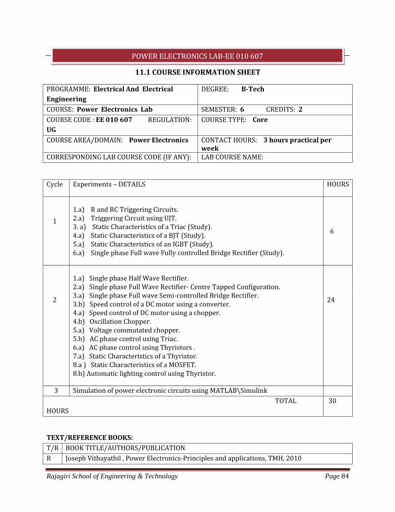
Rajagiri School of Engineering & Technology Page 84
11.1 COURSE INFORMATION SHEET
PROGRAMME: Electrical And Electrical
Engineering
DEGREE: B-Tech
COURSE: Power Electronics Lab SEMESTER: 6 CREDITS: 2
COURSE CODE : EE 010 607 REGULATION:
UG
COURSE TYPE: Core
COURSE AREA/DOMAIN: Power Electronics CONTACT HOURS: 3 hours practical per week
CORRESPONDING LAB COURSE CODE (IF ANY): LAB COURSE NAME:
Cycle Experiments – DETAILS
HOURS
1
1.a) R and RC Triggering Circuits.
6
2.a) Triggering Circuit using UJT. 3. a) Static Characteristics of a Triac (Study). 4.a) Static Characteristics of a BJT (Study). 5.a) Static Characteristics of an IGBT (Study). 6.a) Single phase Full wave Fully controlled Bridge Rectifier (Study).
2
1.a) Single phase Half Wave Rectifier.
24
2.a) Single phase Full Wave Rectifier- Centre Tapped Configuration. 3.a) Single phase Full wave Semi-controlled Bridge Rectifier. 3.b) Speed control of a DC motor using a converter. 4.a) Speed control of DC motor using a chopper. 4.b) Oscillation Chopper. 5.a) Voltage commutated chopper. 5.b) AC phase control using Triac. 6.a) AC phase control using Thyristors . 7.a) Static Characteristics of a Thyristor. 8.a ) Static Characteristics of a MOSFET. 8.b) Automatic lighting control using Thyristor.
3 Simulation of power electronic circuits using MATLAB\Simulink
TOTAL
HOURS
30
TEXT/REFERENCE BOOKS:
T/R BOOK TITLE/AUTHORS/PUBLICATION
R Joseph Vithayathil , Power Electronics-Principles and applications, TMH, 2010
POWER ELECTRONICS LAB-EE 010 607

Rajagiri School of Engineering & Technology Page 85
R M.H. Rashid , Power Electronics – Circuits, Devices and Applications, PHI/Pearson 2005
COURSE PRE-REQUISITES:
C.CODE COURSE NAME DESCRIPTION SEM
EE 010 504 Power Electronics Students studies theory in this paper V
COURSE OBJECTIVES:
1 To provide experience on design and analysis of power electronic circuits used for power electronic applications.
COURSE OUTCOMES:
SNO DESCRIPTION Bloom’s Taxonomy Level
1 Graduates will be able to identify and explain different circuits and corresponding waveforms in power electronic circuits
Comprehension [Level 2]
2 Graduates will be able to select a firing circuit based on the application.
Synthesis [Level 5]
3 Graduates will be able to recognize various power semiconductor devices that are used in power electronic applications
Evaluation [Level 6]
4 Graduates will learn to assess basic concepts used to model different power electronic circuits.
Application [Level 3]
5 Graduates canrecallthe basic concepts which can be applied in advanced power electronic circuits.
Knowledge [Level 1]
MAPPING COURSE OUTCOMES (COs) – PROGRAM OUTCOMES (POs) AND COURSE OUTCOMES (COs) –
PROGRAM SPECIFIC OUTCOMES (PSOs)
PO 1 PO 2 PO 3 PO 4 PO 5 PO 6 PO 7 PO 8 PO 9 PO 10 PO 11 PO 12 PSO 1 PSO 2 PSO 3
C 607.1 3 3 3 3 2
C 607. 2 2 3 3 3 2
C 607. 3 3 2 3 3 3
C 607. 4 3 2 2 1 3 3
C 607. 5 2 3 3 3 3 1
EE 607 1 2 1 2 1 1 1 1 1 1 1 3 3 1
JUSTIFICATIONS FOR CO-PO MAPPING
Mapping L/H/M Justification
C607.1-PO1 H Students will be able to apply knowledge of mathematics and engineering

Rajagiri School of Engineering & Technology Page 86
fundamentals to design power electronic circuits
C607.1-PO2 H By reviewing research literature students will be able to formulate
innovative designs of power electronic circuits.
C607.1-PO4
H Students will be able to conduct experiments, analyze the circuit and
interpret the waveforms.
C607.2-PO1 M Students will be able to apply fundamental knowledge of mathematics and
engineering to design firing circuits.
C607.2-PO4 H Students will be able to select appropriate firing circuits to conduct
experiments.
C607.2-PO5 H Students will be able to model various firing circuits using
MATLAB/Simulink and predict its performance.
C607.3-PO2 H Students will be able to identify and analyze the characteristics of different
semiconductor devices.
C607.3-PO9 M Students can work as a team to choose a semiconductor device based on the
application.
C607.3-PO11
H Students will be able to select system components considering the
economic aspects.
C607.4-PO3 H Students will be able to design power electronic circuits for catering the
technical needs of the society.
C607.4-PO7
M By using the basic knowledge students can propose energy efficient
solutions for power electronic applications.
C607.4-PO10
M Students will be able to give an effective presentation on power electonics
and its applications.
C607.4-PO12 L Student will get an initiation to study different power electronic circuits.
C607.5-PO2 M Students will be able to design power electronics circuits for practical
applications.
C607.5-PO6 H Students will be able to design power electronic circuits such as volatge
regulators and inverters that is beneficial to the society.
C607.5-PO12 H Student will be engaged in updating the emerging trends in the field of
power electronics.
GAPS IN THE SYLLABUS - TO MEET INDUSTRY/PROFESSION REQUIREMENTS:
SNO DESCRIPTION PROPOSED ACTIONS
1 Need to include microcontroller based design of power electronic
circuits
Organize Workshop
PROPOSED ACTIONS: TOPICS BEYOND SYLLABUS/ASSIGNMENT/INDUSTRY VISIT/GUEST
LECTURER/NPTEL ETC
TOPICS BEYOND SYLLABUS/ADVANCED TOPICS/DESIGN:
1 Introduced simulations that can be applied in advanced power electronic circuits

Rajagiri School of Engineering & Technology Page 87
WEB SOURCE REFERENCES:
1
Prof. Kishore Chatterjee and Prof. B.G. Fernandes, Power Electronics,www.nptel.com , Retrieved January 03, 2013, from URL : http://nptel.iitm.ac.in/syllabus/syllabus.php?subjectId=108101038
DELIVERY/INSTRUCTIONAL METHODOLOGIES:
CHALK & TALK STUD.
ASSIGNMENT
WEB RESOURCES
LCD/SMART
BOARDS
STUD. SEMINARS ADD-ON COURSES
ASSESSMENT METHODOLOGIES-DIRECT
ASSIGNMENTS STUD. SEMINARS TESTS/MODEL
EXAMS
UNIV.
EXAMINATION
STUD. LAB
PRACTICES
STUD. VIVA MINI/MAJOR
PROJECTS
CERTIFICATIONS
ADD-ON COURSES OTHERS
ASSESSMENT METHODOLOGIES-INDIRECT
ASSESSMENT OF COURSE OUTCOMES (BY
FEEDBACK, ONCE)
STUDENT FEEDBACK ON FACULTY
(TWICE)
ASSESSMENT OF MINI/MAJOR PROJECTS BY
EXT. EXPERTS
OTHERS
Prepared by Approved by
Mr. Ginnes K John Ms.Santhi B
Ms. Sreepriya R HOD
11.2 COURSE PLAN

Rajagiri School of Engineering & Technology Page 88
Sl.No Module Planned
Date
Planned
1 1 A 27-Jan-16 R and RC Triggering circuits
2 1 B 02-Feb-16 R and RC Triggering circuits
3 1 A 03-Feb-16 UJT Triggering circuits
4 1 B 09-Feb-16 UJT Triggering circuits
5 2A 10-Feb-16 Static Characteristics of a Thyristor.
6 2B 16-Feb-16 Static Characteristics of a Thyristor.
7 2A 17-Feb-16 Static Characteristics of a MOSFET.
8 2B 23-Feb-16 Static Characteristics of a MOSFET.
9 2A 02-Mar-16 Single phase Half Wave Rectifier.
10 2B 09-Mar-16 Single phase Half Wave Rectifier.
11 2A 16-Mar-16 Single phase Full Wave Rectifier- Centre Tapped Configuration
12 2B 17-Mar-16 Single phase Full Wave Rectifier- Centre Tapped Configuration
13 2A 23-Mar-16
a) Single phase Full wave Semi-controlled Bridge Rectifier. b) Speed control of a DC motor using a converter.
14 2 B 24-Mar-16
a) Single phase Full wave Semi-controlled Bridge Rectifier. b) Speed control of a DC motor using a converter.
15 2A 30-Mar-16 a) Speed control of DC motor using a chopper. b) Oscillation Chopper.
16 2 B 31-Mar-16 a) Speed control of DC motor using a chopper. b) Oscillation Chopper.
17 2 A 06-Apr-16
a)Voltage commutated chopper. b) AC phase control using Triac.
18 2B 07-Apr-16 a)Voltage commutated chopper. b) AC phase control using Triac.
19 2 A 20-Apr-16 AC phase control using Thyristors
20 2 B 21-Apr-14 AC phase control using Thyristors

Rajagiri School of Engineering & Technology Page 89
11.3 ADVANCED QUESTIONS
Static Characteristics of a Thyristor
QE3. Design and setup a circuit to plot static V-I characteristics of the given thyristor TYN616.
What is the minimum value of gate voltage and gate current to turn ON the device TYN 616?
Static characteristics of a triac QE6. setup an experiment to plot static V-I characteristics of the device which can be operated
on both first and third quadrant.
Static characteristics of a power BJT QE9. Design and setup a circuit to plot collector emitter voltage versus collector current for a
constant base current of the given device 2N3055.
Static characteristics of a power MOSFET QE12. Setup an experiment to plot transfer and output characteristics of the given MOSFET.
Static characteristics of an IGBT
QE15. Setup an experiment to plot transfer and output characteristics of the given IGBT.
ADVANCED QUESTIONS – DESIGN AND TESTING
R triggering
Q. Design a triggering circuit to obtain the following voltage waveform. Consider the firing
angle α=30º. The triggering circuit should not have any capacitor. Given 230/24 V transformer.
RC Triggering
Q. Design and setup a triggering circuit to obtain following waveform. The firing circuit has only
passive components in the triggering part. Given 230/24 V Transformer
0 0.01 0.02 0.03 0.04 0.05 0.06-50
0
50Source Voltage
0 0.01 0.02 0.03 0.04 0.05 0.06-1
0
1
2Gate Voltage
0 0.01 0.02 0.03 0.04 0.05 0.06-20
0
20
40Voltage Across Load / Output Voltage
0 0.01 0.02 0.03 0.04 0.05 0.06-40
-20
0
20
Time in seconds
Voltage Across Thyristor
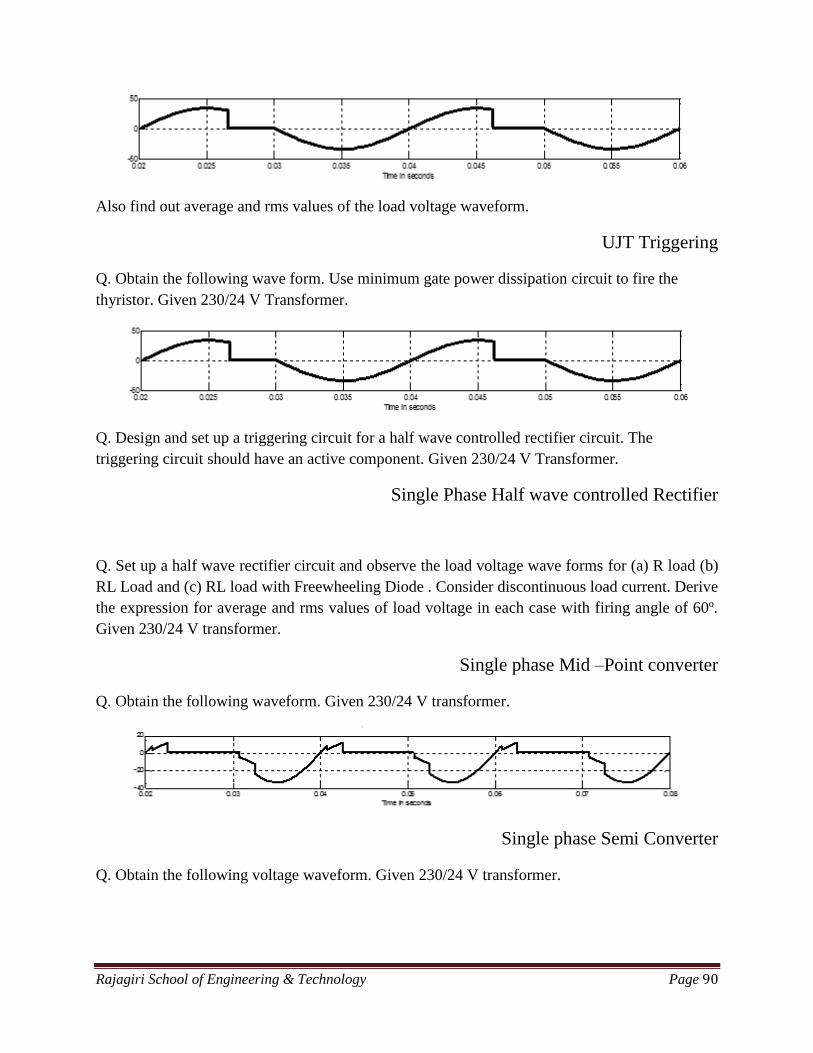
Rajagiri School of Engineering & Technology Page 90
Also find out average and rms values of the load voltage waveform.
UJT Triggering
Q. Obtain the following wave form. Use minimum gate power dissipation circuit to fire the
thyristor. Given 230/24 V Transformer.
Q. Design and set up a triggering circuit for a half wave controlled rectifier circuit. The
triggering circuit should have an active component. Given 230/24 V Transformer.
Single Phase Half wave controlled Rectifier
Q. Set up a half wave rectifier circuit and observe the load voltage wave forms for (a) R load (b)
RL Load and (c) RL load with Freewheeling Diode . Consider discontinuous load current. Derive
the expression for average and rms values of load voltage in each case with firing angle of 60º.
Given 230/24 V transformer.
Single phase Mid –Point converter
Q. Obtain the following waveform. Given 230/24 V transformer.
Single phase Semi Converter
Q. Obtain the following voltage waveform. Given 230/24 V transformer.

Rajagiri School of Engineering & Technology Page 91
Use only one controllable semiconductor device in the circuit.
Single Phase Fully Controlled Bridge Rectifier
Q. Obtain the following voltage waveform using a controlled rectifier circuit. Given 230/24 V
transformer.
Speed Control of a DC Motor Using a Controlled Rectifier
Qn.) Design and set up a circuit to plot the speed of the motor verses armature voltage when 24
V PMDC motor is connected to single phase half controlled rectifier. Given 230/24V
transformer.
AC Voltage Regulator Using Thyristors
Qn.) Obtain the following voltage waveform. Use only one controllable power semiconductor
device. Given 230/24 V transformer.
AC Voltage Regulator Using a Triac
Qn) Design a circuit to obtain the following voltage waveform using bidirectional conducting
power semiconductor device. Pre-determine and calculate the rms value of the given waveform
for a firing angle α=45º. Given 230/24 V transformer.
Complementary Commutation Circuit
0 0.01 0.02 0.03 0.04 0.05 0.06-50
0
50Source Voltage
0 0.01 0.02 0.03 0.04 0.05 0.06-50
0
50Load Voltage
0 0.01 0.02 0.03 0.04 0.05 0.060
0.2
0.4Load Current
0 0.01 0.02 0.03 0.04 0.05 0.060
20
40
Time in seconds
Voltage Across Thyristor1
0 0.01 0.02 0.03 0.04 0.05 0.06 0.07 0.08-50
0
50Source Voltage
0 0.01 0.02 0.03 0.04 0.05 0.06 0.07 0.08-50
0
50Load Voltage
0 0.01 0.02 0.03 0.04 0.05 0.06 0.07 0.08-0.5
0
0.5Load Current
0.02 0.03 0.04 0.05 0.06 0.07 0.08
-20
0
20
40
Time in seconds
Voltage Across Thyristor T1 or T2
0 0.01 0.02 0.03 0.04 0.05 0.06-50
0
50Source Voltage
0 0.01 0.02 0.03 0.04 0.05 0.06-50
0
50Load Voltage
0 0.01 0.02 0.03 0.04 0.05 0.06-0.5
0
0.5Load Current
0 0.01 0.02 0.03 0.04 0.05 0.06-20
0
20
40
Time in seconds
Voltage Across Thyristor 1
0 0.01 0.02 0.03 0.04 0.05 0.06 0.07 0.08-50
0
50Source Voltage
0 0.01 0.02 0.03 0.04 0.05 0.06 0.07 0.08-50
0
50Load Voltage
0 0.01 0.02 0.03 0.04 0.05 0.06 0.07 0.08-0.5
0
0.5Load Current
0 0.01 0.02 0.03 0.04 0.05 0.06 0.07 0.08-50
0
50
Time in seconds
Voltage Across Thyristor 1

Rajagiri School of Engineering & Technology Page 92
Q. Identify the circuit to obtain the following voltage waveforms. Design and setup the circuit
and plot the waveforms. Given 12 V DC supply.
Q. Design and setup a commutation circuit whose power semiconductor devices voltage
waveforms are given below.
Resonance Commutation Circuit
Q. Design and setup a forced commutation circuit which works on the principle of current
commutation technique. Given 12 V DC supply.
Q. Identify the commutation circuit whose commutation element current waveform is shown
below. Design and setup the commutation circuit. Given 12V DC supply.
Impulse Commutation Circuit
Q. Design and setup an impulse commutation circuit. Plot the relevant waveforms. Given 24V
and 12V DC supply.
Q. Identify the commutation circuit whose commutation element current waveform is shown
below. Design and setup the commutation circuit. Given 24V and 12V DC supply.
Current Commutated Chopper or Oscillation Chopper
0 0.005 0.01 0.015 0.02 0.025 0.03 0.035 0.04-20
0
20Capacitor Voltage
0 0.005 0.01 0.015 0.02 0.025 0.03 0.035 0.04-20
0
20Voltage Across Main Thyristor
0.01 0.015 0.02 0.025 0.03 0.035 0.04
-10
0
10
Capacitor Voltage
0.01 0.015 0.02 0.025 0.03 0.035 0.04-10
0
10
20
30
Time in seconds
Load Voltage
0 0.005 0.01 0.015 0.02 0.025 0.03 0.035 0.04-1
0
1Capacitor Voltage
0 0.005 0.01 0.015 0.02 0.025 0.03 0.035 0.04-20
0
20
40Voltage Across Main Thyristor
0.01 0.015 0.02 0.025 0.03 0.035 0.04
-10
0
10
Power semi conductor device Voltage waveform 1
0.01 0.015 0.02 0.025 0.03 0.035 0.04
-10
0
10
Time in seconds
Power semi conductor device Voltage waveform 2
0 0.01 0.02 0.03 0.04 0.05 0.06-20
0
20Capacitor Currrent
0 0.01 0.02 0.03 0.04 0.05 0.06-10
0
10
20Load Voltage ( Voltage across Load Resistor,R )
0 0.01 0.02 0.03 0.04 0.05 0.06-10
0
10
20Voltage Across Thyristor
0 0.01 0.02 0.03 0.04 0.05 0.06
-0.2
0
0.2
Time in seconds
Current through the commutating element
0 0.005 0.01 0.015 0.02 0.025 0.03 0.035 0.04-100
0
100Capacitor Current
0 0.005 0.01 0.015 0.02 0.025 0.03 0.035 0.04-100
0
100Voltage Across the Capacitor
0 0.005 0.01 0.015 0.02 0.025 0.03 0.035 0.04-2
0
2Voltage Across the Auxiliary Thyristor
0.01 0.015 0.02 0.025 0.03 0.035 0.04-1
0
1
Time in seconds
Current through the commutating element

Rajagiri School of Engineering & Technology Page 93
Qn.) Design and set up a circuit to obtain following waveforms that works on the principle of
LC resonance. Identify the control strategy which is used here. Explain how to achieve the same.
Given 12 V DC.
Voltage Commutated Chopper
Q. Design and set up a circuit to obtain following waveforms that work on the principle of
impulse commutation. Given 24V and 12V DC supply. Identify the control technique which is
used here.
Q. Design and set up a circuit to obtain following waveforms where main thyristor is turned OFF
using a negative voltage. Given 24V and 12V DC supply. Identify the control technique which is
used here.
0 0.005 0.01 0.015 0.02 0.025 0.03 0.035 0.04-5
0
5
10
15Load Voltage 1
0 0.005 0.01 0.015 0.02 0.025 0.03 0.035 0.04-5
0
5
10
15
20
Time in seconds
Load Voltage 2
0 0.001 0.002 0.003 0.004 0.005 0.006 0.007 0.008 0.009 0.01-10
0
10
20
30
40
50Load Voltage - 1
0 0.001 0.002 0.003 0.004 0.005 0.006 0.007 0.008 0.009 0.01-10
0
10
20
30
40
Time in seconds
Load Voltage - 2

Rajagiri School of Engineering & Technology Page 94
ADVANCED QUESTIONS – Simulation Simulation - R triggering
Q. Design and simulate a R triggering circuit for the following parameters
(a)Input voltage of 200V (max value) & 50Hz
(b)Firing angle α = 300
and
(c)RLoad=100Ω.
Observe the waveforms of load voltage and load current and comment on result.
Simulation - RC triggering Q. Design and simulate a half wave RC triggering circuit with the following parameters
(a) Input voltage of 200V (max value) & 50Hz
(b) Firing angle α = 1300
and
(c) RLoad = 100Ω.
Observe the following waveforms: source voltage, load voltage, load current & source current
and comment on the result.
Simulation- Half wave rectifier
Q. Design and simulate a single phase half wave rectifier with the following parameters
(a) Input voltage of 120V (RMS value) & 50Hz
(b) Firing angle α=1000
and
(c) RLoad=100Ω.
0 0.002 0.004 0.006 0.008 0.01 0.012-10
0
10
20
30
40
50Load Voltage - 1
0 0.002 0.004 0.006 0.008 0.01 0.012-10
0
10
20
30
40
50
Time in seconds
Load Voltage - 2
Rajagiri School of Engineering & Technology Page 95
Analyse the waveforms of source voltage, load voltage, load current, and source current under
following conditions
a. Resistive Inductive load – Continous or Discontinous Conduction Mode
b. Resistive Inductive load with Freewheeling diode – Continous or Discontinous Conduction
Mode
How can we say that the input power factor is improved by keeping a freewheeling diode in the
circuit? Comment on it by comparing source current waveforms.
Simulation – Mid Point converter
Q. Simulate a single phase mid-point converter with the following parameters
(a) Input voltage of 120V (RMS value) & 50Hz
(b) Firing angle α = 900
and
(c) RLoad = 100Ω.
Analyses the waveforms of secondary winding voltage, load voltage, load current, freewheeling
diode current and voltage across the thyristor under following load conditions
(a) Resistive-Inductive load and Freewheeling Diode– Discontinous Conduction Mode
(b).Resistive-Inductive load and Freewheeling Diode– Continous Conduction Mode
(c) Resistive-Inductive-Back EMF load and with Freewheeling diode - Discontinous Conduction
Mode
(d) Resistive-Inductive-Back EMF load and with Freewheeling diode - Continous Conduction
Mode
Predetermine the average and RMS value of the load voltage under each load conditions and
verify it by simulation.
How can we say that the input power factor is improved by keeping a freewheeling diode in the
circuit?
.Simulation- semi converter
Q. Design and simulate a single phase semi-converter circuit with the following parameters
1. Input voltage of 120V (RMS value) & 50Hz
2. Firing angle α = 1000
and
3. RLoad = 100Ω.
Analyse the waveforms of source voltage, load voltage, load current, and source current under
following conditions
a. Resistive Inductive load - Continous or Discontinous Conduction Mode
b. Resistive Inductive load with Freewheeling diode – Continous or Discontinous Conduction
Mode
How can we say that the input power factor is improved by keeping a freewheeling diode in the
circuit?
Simulation- single phase full converter

Rajagiri School of Engineering & Technology Page 96
Q. Design and simulate a single phase full converter circuit with the following parameters
(1) Input voltage of 120V (RMS value) and 50Hz
(2) Firing angle α = 600
and
(3) RLoad = 100Ω.
Analyses the waveforms of source voltage, voltage across the load, load current, freewheeling
diode current and voltage across the thyristor T1 under following conditions
(a) Purely resistive load
(b) Resistive-Inductive load – Discontinous Conduction Mode
(c) Resistive-Inductive load - Continous conduction Mode
(d)Resistive-Inductive-Back EMF load with Freewheeling diode - Discontinous
Conduction Mode
(e) Resistive-Inductive-Back EMF load with Freewheeling diode - Continous Conduction
Mode
Predetermine the average and RMS value of the load voltage under each load conditions and
verify it by simulation. Assume the values of inductance L and back emf E.
Simulation – single phase AC voltage controller
Q. Simulate a single phase AC voltage controller circuit with following parameters
a) AC supply voltage = 230V RMS and Supply frequency = 50 Hz
b) R = 100 Ω
c) Firing angle, α = 30º
Analyses and plot the following waveforms
(1) Supply voltage (2) Load voltage (3) Load current (4) Voltage across Thyristor 1 and
(5) Voltage across Thyristor 2
Perform the operation with RL load. Choose the load inductor value L such that the load current
is discontinuous.
simulation - Complimentary Commutation Circuit
Q. Design and simulate a complementary commutation circuit with following parameters
(a) DC supply voltage = 24V
(b) Load Resistor = 100Ω
(c) Switching period = 8msec and select appropriate ON time
Observe the following waveforms:
1. Capacitor voltage
2. Voltage across main thyristor
3. Voltage across complementary thyristor
4. Load voltage.

Rajagiri School of Engineering & Technology Page 97
Q. Design and simulate the parallel resonance commutation circuit for a thyristor with following
parameters
(a) DC supply voltage = 12V
(b) Load Resistor = 50Ω
(c) Switching period = 10msec
Observe the following waveforms:
(1) Capacitor current
(2) Load current
(3) Current through the thyristor
(4) Load voltage (5) Voltage across the thyristor
Simulation - Impulse Commutation Circuit Q. Design and simulate a commutation circuit which uses impulse voltage to turn off the
thyristor with following parameters.
(1) DC supply voltage = 24V
(2) Load Resistor = 150Ω
(2) Switching period = 15msec
Observe and plot the following waveforms:
(a) Capacitor current
(b) Voltage across the capacitor
(c) Current through the main thyristor
(d) Voltage across main thyristor
(e) Voltage across auxiliary thyristor
(f) Load voltage
Simulation- Oscillation chopper
Q. Design and simulate an oscillation chopper circuit with following parameters
a) DC supply voltage = 12V
b) tOFF = 0.66 msec
c) Chopping frequency = 100 Hz
Analyse and plot the following waveforms
(1) Capacitor voltage (2) Load voltage (3) Thyristor voltage and (4) Thyristor current
Perform constant and variable frequency operation of oscillation chopper. For variable frequency
operation choose chopping frequency as 200 Hz.
Compare the waveforms with above question.
Simulation - voltage commutated chopper

Rajagiri School of Engineering & Technology Page 98
Q. Design and simulate a voltage commutated chopper circuit with following parameters
a) DC supply voltage = 12V
b) tOFF = 0.66 msec
c) Chopping frequency = 100 Hz
Analyse and plot the following waveforms
(1) Capacitor voltage (2) Load voltage (3) Thyristor voltage and (4) Thyristor current.
Perform constant and variable frequency operation of oscillation chopper. For variable frequency
operation choose chopping frequency as 200 Hz.
simulation – Buck converter
Q. Design and simulate a buck regulator circuit for the following parameters
(a) Input voltage = 10V DC
(b) Switching frequency = 10kHz
(c) Output voltage = 8V
Observe and analyses the waveforms of voltage across the load, inductor voltage, inductor
current and capacitor current.
Perform both continuous and discontinuous operation of the circuit.
simulation – Boost converter
Q. Design and simulate a boost regulator circuit with the following parameters
(a)Input voltage 12V DC
(b) Switching frequency =10 kHz
(c)Output voltage = 18V
Observe and analyses voltage across the load, inductor voltage, inductor current, capacitor
current, load current and voltage across the switch.
Simulation – Single phase inverter
Q. Simulate a single phase inverter circuit having a DC source voltage of 220V with Resistance-
Inductance load. Take switch as IGBT and & .R L mH 100 100Ω Observe following
waveforms
(a) Input voltage (b) Load voltage (c) Load current (d) Pulses to the gate of the switches and (e)
current flowing through a switch and its anti-parallel diode.
Also do FFT analysis on the load voltage and the load current waveforms. Find out THD in each
case and comment on harmonic values obtained.
Simulation- Three phase inverter

Rajagiri School of Engineering & Technology Page 99
Q. Simulate a three phase inverter circuit having a DC voltage source of 220V with a three
phase star connected Resistance-Inductance load. Select IGBTs as the switches and R = 100Ω
and L = 100mH.
Observe following waveforms for both 1800 and 120
0conduction mode.
(a) Phase voltages VAN, VBN, VCN (b) Line voltages VAB, VBC, VCA (c) Current in the each phase
of the load (d) Pulses to the gate of the switches (e) Current flowing through a switch and its
anti-parallel diode.
Observe current waveform in any one phase of the load and through a switch and its anti parallel
diode and comment on it.
11.4 OPEN QUESTIONS
CHARACTERISTICS OF DEVICES
Static Characteristics of a Thyristor
QE1. Set up an experiment to plot static V-I characteristics of given device TYN 616. Find out
minimum gate voltage and gate current to turn ON the device.
QE2. What you meant by latching current and holding current. Set up an experiment to obtain
these values practically. Given TYN 616 device. Also plot forward characteristics.
Static characteristics of a triac
QE4. Set up an experiment to plot static V-I characteristics of given device BT 136.
QE5. Design and setup a circuit to plot forward and reverse characteristics of the device BT 136.
Static characteristics of a power BJT
QE7. Setup an experiment to find input characteristics of the given device 2N3055.
QE8. Design and setup a circuit to plot input characteristics and output characteristics of
2N3055.
Static characteristics of a power MOSFET QE10. Setup an experiment to find threshold voltage of IRF 740. Also plot its transfer
characteristics.

Rajagiri School of Engineering & Technology Page 100
QE11. Design and setup a circuit to plot transfer characteristics and output characteristics of IRF
740.
Static characteristics of an IGBT
QE13. Setup an experiment to find threshold voltage of CT60. Also plot its transfer
characteristics.
QE14. Design and setup a circuit to plot transfer characteristics and output characteristics of
CT60.
OPEN QUESTIONS – DESIGN AND TESTING
R triggering
Q. Design and set up a firing circuit that trigger a thyristor with maximum firing angle of 90 0 .
Derive the RMS and average value of output voltage and pre determine the values for the firing
angle of 45º. Obtain and plot following waveforms at the firing angle α=45 0 .
(a) Source voltage (b) load voltage and (c) voltage across the thyristor. Given 230/24 V
Transformer
Q. Design and set up a half wave controlled rectifier with a firing circuit having maximum firing
angle of 90 0 . Draw the relevant wave forms. Given 230/24 V Transformer
RC Triggering
Q. Design and set up a triggering circuit to obtain following waveform. The firing circuit has the
firing angle maximum of 180º.
Also obtain relevant wave forms at the power side for α=120º. Given 230/24 V Transformer.
Predetermine average and rms values of the load voltage.

Rajagiri School of Engineering & Technology Page 101
Q. Design and set up RC full wave triggering circuit. Obtain relevant wave forms at the power
side for α=30º. Given 230/24 V Transformer.
UJT Triggering
7. Design and set up a half wave controlled rectifier by using UJT firing circuit .Draw relevant
waveforms both at power side and control side for α=45º. Pre-determine the average and rms
values of the load voltage. Given 230/24 V Transformer.
8. Design and set up a full wave controlled rectifier by using UJT firing circuit .Draw relevant
waveforms both at power side and control side for α=90º. Pre-determine the average and rms
values of the load voltage. Given 230/24 V Transformer.
9. Design and set up a triggering circuit for half wave controlled rectifier with firing angle of
α=120º which has good reliability and satisfactory operation over a wide range of temperature.
Given 230/24 V Transformer.
Single Phase Half wave controlled Rectifier
Q. Design and set up an experiment to observe the wave forms at firing angle of α=60º for single
phase half wave rectifier circuit with Resistive load. Derive and pre-determine the average and
rms values of the load voltage. Given 230/24 V transformer.
Single phase Mid –Point converter
Q. Design and Set up an experiment to obtain a waveform for fully controlled rectified load
voltage when each thyristor has a peak inverse voltage (PIV) of 2Vm appearing across it. Given
230/24 V transformer.
Q. Observe and plot the waveforms for a single phase full wave rectifier with centre-tapped
configuration having RL load under discontinuous mode operation. Given 230/24 V
transformer.
Single phase Semi Converter
Q. Observe and plot the load voltage wave form for a single phase semi converter for (a) R load
(b) RL load and (c) RL load with freewheeling Diode, under discontinuous mode operation.
Derive the expression of RMS value of the load voltage when firing angle is α=45º under each
case. Comment on your observations. Given 230/24 V transformer
Q. Observe the Load voltage wave form by setting up a suitable rectifier circuit such that, it can
operate only in one quadrant. Take the load as RL load. Given 230/24 V transformer.
Single Phase Fully Controlled Bridge Rectifier

Rajagiri School of Engineering & Technology Page 102
Q. Design and setup a single phase rectifier circuit which can operate in two quadrants. Given
230/24 V transformer. Pre-determine the average and rms values of the load voltage for any
firing angle.
Speed Control of a DC Motor Using a Controlled Rectifier
Qn.) Design and set up a circuit to plot the speed of the motor versus armature voltage. Given
24V, 1500 RPM PMDC motor and 230/24 V transformer.
AC Voltage Regulator Using Thyristors
Qn.) Obtain the following voltage waveform using unidirectional conducting power
semiconductor devices. Pre-determine and calculate the rms value of the load voltage for a firing
angle α=30º. Given 230/24 V transformer.
Qn.) Set up a power electronic circuit that controls AC voltage using unidirectional controllable
devices. Get the following current waveform. Given 230/24 V transformer.
AC Voltage Regulator Using a Triac
Qn.) Design a circuit to obtain the following voltage waveform using bidirectional conducting
power semiconductor device. Pre-determine and calculate the rms value of the load voltage for a
firing angle α=45º. Given 230/24 V transformer.
Current Commutated Chopper or Oscillation Chopper Q. Design and set up an oscillation chopper circuit and plot its wave forms. Also perform
constant and variable frequency operation. Given 12 V DC supply.
0 0.01 0.02 0.03 0.04 0.05 0.06-50
0
50Source Voltage
0 0.01 0.02 0.03 0.04 0.05 0.06-50
0
50Load Voltage
0 0.01 0.02 0.03 0.04 0.05 0.06-0.5
0
0.5Load Current
0 0.01 0.02 0.03 0.04 0.05 0.06-50
0
50
Time in seconds
Voltage Across Thyristor 1

Rajagiri School of Engineering & Technology Page 103
Q. Design and set up a circuit to obtain following waveform that works on the principle of LC
resonance. Given 12 V DC supply
Voltage Commutated Chopper
Q. Design and set up a voltage commutated chopper and plot its wave forms. Given 24 V and
12V DC supply. Obtain experimentally two types of time ratio control (TRC) schemes.
0 0.005 0.01 0.015 0.02 0.025 0.03-5
0
5
10
15
20Load Voltage
0 0.005 0.01 0.015 0.02 0.025 0.03-5
0
5
10
15
Time in seconds
Load Voltage

Rajagiri School of Engineering & Technology Page 104
OPEN QUESTIONS – Simulation Simulation - R triggering
Q. Design and simulate an R triggering circuit for the following parameters:
(a) Input voltage of 325V (max value) & 50Hz
(b) Firing angle α = 450
and
(c) RLoad = 100Ω.
Observe and note down the source voltage, output voltage or voltage across the load, gate
voltage and voltage across the thyristor.
Simulation - RC triggering Q. Design and simulate a half wave RC triggering circuit with the following parameters
(a) Input voltage of 325V (max value) and 50Hz
(b) Firing angle α = 750
and
(c) RLoad = 100Ω.
Observe the following waveforms: source voltage, voltage across the load, capacitor
voltage and voltage across the thyristor.
Simulation- Half wave rectifier
Q. Design and simulate a single phase half wave rectifier with the following parameters
(a)Input voltage of 325V (max value) & 50Hz
(b)Firing angle α = 450
and
(c) RLoad = 100Ω.
Analyses the waveforms of source voltage, load voltage, load current and voltage across the
thyristor under following load conditions
a. Purely resistive load
b. Resistive-Inductive load – Discontinous Conduction Mode
c. Resistive-Inductive-Back EMF load - Discontinous conduction Mode
d. Resistive-Inductive-Back EMF load & with Freewheeling diode - Discontinous Conduction
Mode
e. Resistive-Inductive-Back EMF load & with Freewheeling diode - Continous Conduction
Mode
Predetermine the average and RMS value of the load voltage under each load conditions and
verify it by simulation.
Q. Design and simulate a single phase half wave rectifier with the following parameters
(a)Input voltage of 120V (RMS value) & 50Hz
(b)Firing angle α=300
and
(c) RLoad=100Ω.
Analyses the waveforms of source voltage, load voltage, load current, freewheeling diode current
and voltage across the thyristor under following conditions
a. Purely resistive load

Rajagiri School of Engineering & Technology Page 105
b. Resistive-Inductive load – Discontinous Conduction Mode
c. Resistive-Inductive-Back EMF load – Discontinous conduction Mode
d. Resistive-Inductive-Back EMF load & with Freewheeling diode – Discontinous Conduction
Mode
e. Resistive-Inductive-Back EMF load & with Freewheeling diode – Continous Conduction
Mode
Predetermine the average and RMS value of the load voltage under each load conditions and
verify it by simulation.
Simulation – Mid Point converter
Q. Simulate a single phase mid-point converter with the following parameters
(a)Input voltage of 325V (max value) & 50Hz
(b)Firing angle α = 300
and
(c)RLoad = 100Ω.
Analyses the waveforms of secondary winding voltage, load voltage, load current and voltage
across the thyristor under following load conditions
a. Purely resistive load
b. Resistive-Inductive load – Discontinous Conduction Mode
c. Resistive-Inductive load – Continous Conduction Mode
Predetermine the average and RMS value of the load voltage under each load conditions and
verify it by simulation.
.Simulation- semi converter
Q. Design and simulate a single phase semi-converter circuit with the following parameters
a. Input voltage of 325V (max value) and 50Hz
b. Firing angle α = 350
and
c. RLoad = 100Ω.
Analyses the waveforms of source voltage, load voltage, load current and voltage across the
thyristor under following load conditions
a. Purely resistive load
b. Resistive-Inductive load – Discontinous Conduction Mode
c. Resistive-Inductive-Back EMF load with Freewheeling diode - Discontinous Conduction
Mode
Predetermine the average and RMS value of the load voltage under each load conditions and
verify it by simulation. Assume the values of inductance L and back emf E.
Q. Design and simulate a single phase semi-converter circuit with the following parameters
(a) Input voltage of 120V (RMS value) & 50Hz
(b) Firing angle α = 600
and
(c) RLoad = 100Ω.

Rajagiri School of Engineering & Technology Page 106
Analyse the waveforms of source voltage, voltage across the load, load current, freewheeling
diode current and voltage across the thyristor under following conditions
a. Purely resistive load
b. Resistive-Inductive load – Discontinous Conduction Mode
c. Resistive-Inductive load - Continous conduction Mode
d. Resistive-Inductive-Back EMF load with Freewheeling diode - Discontinous Conduction
Mode
e. Resistive-Inductive-Back EMF load with Freewheeling diode - Continous Conduction Mode
Predetermine the average and RMS value of the load voltage under each load conditions and
verify it by simulation. Assume the values of inductance L and back emf E.
Simulation- single phase full converter
Q. Design and simulate a single phase full converter circuit with the following parameters
(a) Input voltage of 325V (max value) & 50Hz
(b) Firing angle α = 350
and
(c) RLoad = 100Ω.
Analyses the waveforms of source voltage, load voltage, load current and voltage across the
thyristor T1 under following load conditions
(a) Purely resistive load
(b) Resistive-Inductive load – Discontinous Conduction Mode
(c) Resistive-Inductive-Back EMF load with Freewheeling diode - Discontinous
Conduction Mode
Predetermine the average and RMS value of the load voltage under each load conditions and
verify it by simulation. Assume the values of inductance L and back EMF E.
Simulation – single phase AC voltage controller
Q. Simulate a single phase AC voltage controller circuit with following parameters
a) AC supply voltage = 24V RMS and supply frequency = 50 Hz
b) R = 100 Ω
c) Firing angle, α = 45º
Analyses and plot the following waveforms
(1) Supply voltage (2) Load voltage (3) Load current (4) Voltage across Thyristor 1 and
(5) Voltage across Thyristor 2
Perform the operation with RL load. Choose the load inductor value L such that the load current
is discontinuous.
Simulation- Oscillation chopper
Q. Design and simulate an oscillation chopper circuit with following parameters

Rajagiri School of Engineering & Technology Page 107
a) DC supply voltage = 24V
b) tOFF = 0.66 msec
c) Chopping frequency = 100 Hz
Analyse and plot the following waveforms
(1) Capacitor voltage (2) Load voltage (3) Thyristor voltage and (4) Thyristor current.
Perform constant and variable frequency operation of oscillation chopper. For variable frequency
operation choose chopping frequency as 200 Hz.
Simulation - voltage commutated chopper
Q. Design and simulate a voltage commutated chopper circuit with following parameters
a) DC supply voltage = 24V
b) tOFF = 0.66 msec
c) Chopping frequency = 100 Hz
Analyse and plot the following waveforms
(1) Capacitor voltage (2) Load voltage (3) Thyristor voltage and (4)Thyristor current
Perform constant and variable frequency operation of oscillation chopper. For variable frequency
operation choose chopping frequency as 200 Hz.
Simulation – Single phase inverter
Q. Simulate a single phase inverter circuit having a DC source voltage of 220V with Resistance
load of 100Ω. Observe following waveforms
(a) Input voltage (b) Load voltage (c) Load current (d) Pulses to the gate of the switches.
Also do FFT analysis on the load voltage waveform and find out THD.
Q. Simulate a single phase inverter circuit having a DC source voltage of 220V with Resistance-
Inductance load. Take switch as MOSFET and & .R L mH 100 100Ω
Observe following waveforms
(a) Input voltage (b) Load voltage (c) Load current (d) Pulses to the gate of the switches and (e)
current flowing through a switch.
Also do FFT analysis on the load voltage and the load current waveforms. Find out THD of each
case and comment on harmonic values obtained.

Rajagiri School of Engineering & Technology Page 108
Simulation- Three phase inverter
Q. Simulate a three phase inverter circuit having a DC voltage source of 220V with a three
phase star connected Resistance load of 100Ω. Observe following waveforms for both 1800 and
1200 conduction mode.
(a) Phase voltages VAN, VBN, VCN (b) Line voltages VAB, VBC, VCA (c) Pulses to the gate of the
switches (d) Current in the each phase of the load
Also do FFT analysis on the phase and line voltage waveforms and find out THDs. Also
Comment on THDs obtained.
Q. Simulate a three phase inverter circuit having a DC voltage source of 220V with a three phase
star connected Resistance-Inductance load. Select MOSFETs as the switches and R= 100Ω and L
= 100mH.
Observe following waveforms for both 1800 and 120
0conduction mode.
(a)Phase voltages VAN, VBN, VCN (b) Line voltages VAB, VBC, VCA (c) Current in the each phase
of the load (d) Pulses to the gate of the switches. (e) Current flowing through a switch.
Observe current waveform in any one phase of the load and through a switch and comment on it.

Rajagiri School of Engineering & Technology Page 109
12.1 COURSE INFORMATION SHEET
PROGRAMME: Electrical & Electronics
Engineering
DEGREE: B.TECH
COURSE: Microprocessor and
Microcontroller Lab
SEMESTER: VI CREDITS: 2
COURSE CODE: EE 010 608
REGULATION: UG
COURSE TYPE:PRACTICAL
COURSE AREA/DOMAIN: Electronics CONTACT HOURS: 3 hours/Week.
CORRESPONDING LAB COURSE CODE (IF
ANY):
LAB COURSE NAME:
SYLLABUS:
CYCLE DETAILS HOURS
I
1. 8085 assembly language programming experiments
2. Familiarization of 8085 microprocessor and trainer kit
3. 8-bit and 16 bit arithmetic operations
4. Sorting
5. BCD to binary and binary to BCD conversion
6. Finding square root of a number
7. Finding out square root of a number
8. Setting up time delay and square wave generation
9. Interfacing of led and seven segment display.
12
II
10. 8051 PROGRAMMING
11. Familiarization of 8051 microcontroller.
12. Basic arithmetic operations
13. Setting up time delay using timer and square wave generation
14. Interfacing LEDs
15. Interfacing LCD display
12
III 16. MINI PROJECT 6
TOTAL HOURS 30
MICROPROCESSOR & MICROCONTROLLER LAB-EE 010 608

Rajagiri School of Engineering & Technology Page 110
TEXT/REFERENCE BOOKS:
T/R BOOK TITLE/AUTHORS/PUBLICATION
R SATISH SHAH, 8051 MICROCONTROLLER , OXFORD HIGHER EDUCATION
R RAMESH GAONKAR, MICROPROCESSOR ARCHITECTURE, PROGRAMMING AND APPLICATIONS
WITH 8085, PENRAM INTL.
R B.RAM, FUNDAMENTALS OF MICROPROCESSORS AND MICROCOMPUTERS, DHANPATRAI AND
SONS
R MUHAMMAD ALI MAZIDI AND JANICE GILLISPIEMAZIDI, THE 8051 MICROCONTROLLER AND
EMBEDDED SYSTEMS, PEARSON EDUCATION ASIA.
R KENNETH J.AYALA, THE 8051 MICROCONTROLLER – ARCHITECTURE, PROGRAMMING AND
APPLICATIONS, PENRAM INTERNATIONAL PUBLISHING (INDIA),ED 2
COURSE PRE-REQUISITES:
C.CODE COURSE NAME DESCRIPTION SEM
EN010 506 MICROPROCESSORS AND
APPLICATIONS
8085 MICROPROCESSOR
ARCHITECTURE PROGRAMMING
AND INTERFACING
V
EE 010 605 MICROCONTROLLERS AND
EMBEDDED SYSTEMS
8051 MICROCONTROLLER
ARCHITECTURE AND PROGRAMMING
VI
COURSE OBJECTIVES:
1 To provide experience in the programming of 8085 microprocessor and 8051 microcontroller
2 To familiarize with the interfacing applications of 8085 microprocessor and 8051
microcontroller.
COURSE OUTCOMES:
SNO DESCRIPTION Blooms’ Taxonomy Level
1 Students will be able to program and interface
8085 microprocessor
Analysis [Level 4]
2 Students will be able to program and interface
8051 microcontroller
Analysis [Level 4]
3 Students will be able to apply their skills in
practical applications using microcontrollers
and microprocessors
Application [level 3]
MAPPING COURSE OUTCOMES (COs) – PROGRAM OUTCOMES (POs) AND COURSE OUTCOMES (COs) –
PROGRAM SPECIFIC OUTCOMES (PSOs)
PO 1 PO 2 PO 3 PO 4 PO 5 PO 6 PO 7 PO 8 PO 9 PO 10 PO 11 PO 12 PSO 1 PSO 2 PSO 3
C 608.1 2 1 1 1 1 1 1 2 1 1
C 608. 2 2 1 1 1 1 1 1 2 1 1
C 608. 3 2 1 1 1 1 1 1 2 1 1

Rajagiri School of Engineering & Technology Page 111
EE 608 2 1 1 1 1 1 1 2 1 1
JUSTIFATIONS FOR CO-PO MAPPING
Mapping L/H/M Justification
C 608.1-PO1 M Students will be able to make use of their basic knowledge on programming
and interfacing of 8085 microprocessor to find solutions for engineering
problems
C 608.1-PO2 L Students will be able to analyse the problem properly with the help of their
knowledge on microprocessors
C 608.1-PO3 L Students will be able to design solutions for the issues of society with their
knowledge on microprocessors
C 608.1-PO5 L With the help of knowledge on microprocessors and programming they will
be able to extend the area to the modern IT tools for many situations.
C 608.1-PO7 L Students will be able to contribute for the sustainable development of the
society.
C 608.1-PO9 L The knowledge on microprocessors will help students for the team work
C 608.1-PO12 M Stuents will be able to build up their knowlege in advanced systems
C 608.2-PO1 M Students will be able to make use of their basic knowledge on programming
and interfacing of 8051 microcontroller to find solutions for engineering
problems
C 608.2-PO2 L Students will be able to analyse the problem properly with the help of their
knowledge on microcontrollers
C 608.2-PO3 L Students will be able to design solutions for the issues of society with their
knowledge on microcontrollers
C 608.2-PO5 L With the help of knowledge on microcontrollers and programming they will
be able to extend the area to the modern IT tools for many situations.
C 608.2-PO7 L Students will be able to contribute for the sustainable development of the
society.
C 608.2-PO9 L The knowledge on microcontrollers will help students for the team work
C 608.2-PO12 M Stuents will be able to build up their knowlege in advanced systems
C 608.3-PO1 M Students will be able to make use of their basic knowledge microprocessors
and microcontrollers to find solutions for engineering problems
C 608.3-PO2 L Students will be able to analyse the problem properly with the help of their
knowledge on microcontrollers and microprocessors
C 608.3-PO3 L Students will be able to design solutions for the issues of society with their
knowledge on microprocessors and microcontrollers
C 608.3-PO5 L With the help of knowledge on microprocessors and microcontrollers and
programming they will be able to extend the area to the modern IT tools for
many situations.
C 608.3-PO7 L Students will be able to contribute for the sustainable development of the
society.
C 608.3-PO9 L The knowledge on microprocessors and microcontrollers will help students
for the team work
Rajagiri School of Engineering & Technology Page 112
C 608.3-PO12 M Stuents will be able to build up their knowlege in advanced systems
GAPS IN THE SYLLABUS - TO MEET INDUSTRY/PROFESSION REQUIREMENTS:
SNO DESCRIPTION PROPOSED
ACTIONS
RELEVANCE
WITH POs
RELEVANCE
WITH PSOs
1. INTERFACING OF STEPPER MOTORS
TO BE INCLUDED
INCLUDED AS
ADVANCED
EXPERIMENT IN
THE COURSE
1,5,9,11 1, 3
PROPOSED ACTIONS: TOPICS BEYOND SYLLABUS/ASSIGNMENT/INDUSTRY VISIT/GUEST
LECTURER/NPTEL ETC
TOPICS BEYOND SYLLABUS/ADVANCED TOPICS/DESIGN:
SNO DESCRIPTION PROPOSED
ACTIONS
RELEVANCE
WITH POs
RELEVANCE
WITH PSOs
1 IMPLEMENTATION OF TRAFFIC SIGNAL
CONTROL IN A COMPLEX JUNCTION.
PROJECT
WORK
1,5,9,11 1, 3
WEB SOURCE REFERENCES:
1 http://nptel.iitm.ac.in/courses/webcourse contents/iiscbang/microprocessors and
microcontrollers/pdf/lecture_notes/lnm1.pdf
2 Prof. Krishna Kumar (july 2012) microprocessor and controllers www.nptel.com retrieved august
03, 2013, from url : http://nptel.iitm.ac.in/courses/webcourse-contents/iisc
bang/microprocessors%20and%20microcontrollers/new_index1.ht
ml
DELIVERY/INSTRUCTIONAL METHODOLOGIES:
CHALK & TALK STUD. ASSIGNMENT WEB RESOURCES
LCD/SMART
BOARDS
STUD. SEMINARS ADD-ON COURSES
ASSESSMENT METHODOLOGIES-DIRECT
ASSIGNMENTS STUD. SEMINARS TESTS/MODEL
EXAMS
UNIV. EXAMINATION
STUD. LAB
PRACTICES
STUD. VIVA MINI/MAJOR
PROJECTS
CERTIFICATIONS
ADD-ON COURSES OTHERS

Rajagiri School of Engineering & Technology Page 113
ASSESSMENT METHODOLOGIES-INDIRECT
ASSESSMENT OF COURSE OUTCOMES (BY
FEEDBACK, ONCE)
STUDENT FEEDBACK ON FACULTY (TWICE)
ASSESSMENT OF MINI/MAJOR PROJECTS BY
EXT. EXPERTS
OTHERS
Prepared by Approved by
Fr. Mejo Gracevilla CMI Ms. Santhi B
Mr. Jebin Francis HOD EEE
12.2 COURSE PLAN Sl No Module Date Planned
1
1
19-Jan-
17
BATCH B - 1. To familiarize with the 8085 Microprocessor,
the 8085 kit and its various functions. 2. To familiarize with
the instruction sets of 8085 μP and hexcode manual.
2 20-Jan-
17
BATCH A - 1. To familiarize with the 8085 Microprocessor,
the 8085 kit and its various functions. 2. To familiarize with
the instruction sets of 8085 μP and hexcode manual.
3 27-Jan-
17
BATCH A - 3. (a) To add two 8-bit numbers and find its
result. (b) To subtract two 8-bit numbers and find its result.
(c) To add two 16-bit numbers and find its result. (d) To
subtract two 16-bit numbers and find its result.
4 2-Feb-17
BATCH B - 3. (a) To add two 8-bit numbers and find its
result. (b) To subtract two 8-bit numbers and find its result.
(c) To add two 16-bit numbers and find its result. (d) To
subtract two 16-bit numbers and find its result.
5 3-Feb-17
BATCH A - 4. (a) To multiply two 8-bit numbers using
repeated addition method. (b) To divide two 8-bit numbers
using repeated subtraction method.
6 9-Feb-17
BATCH B - 4. (a) To multiply two 8-bit numbers using
repeated addition method. (b) To divide two 8-bit numbers
using repeated subtraction method.
7 10-Feb-
17
BATCH A - 5. (a) To arrange an array of numbers in
ascending order and display the result in consecutive
memory locations. (b) To arrange an array of numbers in
descending order and display the result in consecutive
memory locations.

Rajagiri School of Engineering & Technology Page 114
8 16-Feb-
17
BATCH B - 5. (a) To arrange an array of numbers in
ascending order and display the result in consecutive
memory locations. (b) To arrange an array of numbers in
descending order and display the result in consecutive
memory locations.
9 17-Feb-
17
BATCH A - 6. (a) To convert a given BCD number to its
binary equivalent. (b) To convert a given binary number to
its BCD equivalent. 7. To find the square root of a number
using odd number subtraction.
10 23-Feb-
17
BATCH B - 6. (a) To convert a given BCD number to its
binary equivalent. (b) To convert a given binary number to
its BCD equivalent. 7. To find the square root of a number
using odd number subtraction.
11 2-Mar-
17
BATCH B - 8. To find the square root of a number using
look-up table. 9. To display uppercase alphabets with a time
delay of 1 second on a seven segment display interfaced to
8085 μP using look-up table.
12
2
9-Mar-
17
BATCH B - 10. To generate square waves of the following
configurations and display them on the CRO interfaced to
8085 μP. a. 50% duty cycle, 2 KHz frequency. b. 80% duty
cycle, 1 KHz frequency. 11. To familiarize with the
AT89C51 Microcontroller, simulating, assembling and
burning of AT89C51 µC using LABTOOL/WELLON
software.
13 16-Mar-
17
BATCH B - 12. Arithmetic Operations using 89C51 (a) To
add two 8-bit numbers stored in ports and to find the result.
(b) To subtract two 8-bit numbers stored in ports and find its
result. (c) To multiply two 8-bit numbers stored in ports and
find its result. (d) To divide two 8-bit numbers stored in
ports and find its result. 13. To find the largest number from
an array using 89C51.
14 1 17-Mar-
17
BATCH A - 8. To find the square root of a number using
look-up table. 9. To display uppercase alphabets with a time
delay of 1 second on a seven segment display interfaced to
8085 μP using look-up table.
15 2 23-Mar-
17
BATCH A - 10. To generate square waves of the following
configurations and display them on the CRO interfaced to
8085 μP. a. 50% duty cycle, 2 KHz frequency. b. 80% duty
cycle, 1 KHz frequency. 11. To familiarize with the
AT89C51 Microcontroller, simulating, assembling and
burning of AT89C51 µC using LABTOOL/WELLON
software.
Rajagiri School of Engineering & Technology Page 115
16 24-Mar-
17
BATCH A - 12. Arithmetic Operations using 89C51 (a) To
add two 8-bit numbers stored in ports and to find the result.
(b) To subtract two 8-bit numbers stored in ports and find its
result. (c) To multiply two 8-bit numbers stored in ports and
find its result. (d) To divide two 8-bit numbers stored in
ports and find its result. 13. To find the largest number from
an array using 89C51.
17 30-Mar-
17 BATCH B - Mini Project
18 31-Mar-
17 BATCH A - Mini Project
19 6-Apr-17 BATCH B - Mini Project
20 7-Apr-17 BATCH A - Mini Project

Rajagiri School of Engineering & Technology Page 116
12.3 ADVANCED EXPERIMENTS
PROGRAMMING USING 8085 OR 8051
1. Write a program to extract odd numbers in a given array and find the average of the odd numbers
using 8051.
2. WAP to find factorial of a 8-bit number using 8085.
3. WAP to find NNusing 8085 where N>0
4. WAP to display today‟s date in seven segment display using 8085/8051
5. WAP to display your name in a seven segment display using 8085
6. WAP to find the numbers of multiples of 6 in an array of 8 bytes using INTEL 8085
7. WAP to function as calculator (8085)
8. WAP to generate 10 terms of Fibonacci series using 8085
9. WAP to generate a signal with 50% and 90% duty cycle with 1KHz frequency
10. WAP to separate even numbers from a given data array and find the largest one using 8085/8051
11. WAP to find X3+5X
2 where X>0
12. WAP to evaluate (a+b)2/2 using 8085
13. WAP to convert the given BCD to Hex. If the answer is odd subtract 05 from it otherwise add 02
to it, using 8085.
14. WAP to find the largest and the smallest from an array (Sort and find) using 8085
15. WAP to find (A/B)1/2
, A>B, A>0, B>0, using 8085.
16. Convert the given decimal number to hexadecimal format. If the number is odd add 03 to it.
Otherwise subtract 03 form it using 8085.
17. WAP to separate odd numbers from a given data array and find the smallest one using 8051.
18. WAP to find the mean of first 10 numbers
19. WAP to perform (A+B)/(A-B), where A and B are two positive real numbers and A>B.
20. WAP to find the average of first 5 numbers
21. WAP to generate a square wave of 1KHz (1.5 KHz) frequency using 8051
22. WAP a program to perform 2X2+5X where X>0
23. WAP to perform largest – Smallest in a data array

Rajagiri School of Engineering & Technology Page 117
12.4 OPEN EXPERIMENTS
1. WAP to take mean of first five odd numbers
2. WAP to take mean of first five even numbers
3. Add two real numbers. If sum is positive, make a LED to glow for 1 second otherwise make it
OFF
4. Interface microprocessor with stepper motor. If the number given is 00 make it to rotate in
clockwise direction. If the number given is FF make it to rotate in CCW direction
5. Write a program to do down counter from 33, 32,31…..1
6. WAP to find (A*B)1/2
, where A and B are positive real numbers and A>B
7. WAP to perform X3+2X
2+3X+2
8. WAP to show the output of a Johnson counter using LEDs
9. WAP to show the output of ring counter using LEDs
10. Write a program to find the largest and the smallest numbers of the given data array and perform
(Largest/Smallest)1/2
11. WAP to find the count of odd parity and even parity numbers in a data array and perform
(O+E/O-E) where O- count of odd parity numbers and E-count of even parity numbers