Embed Size (px)
Citation preview
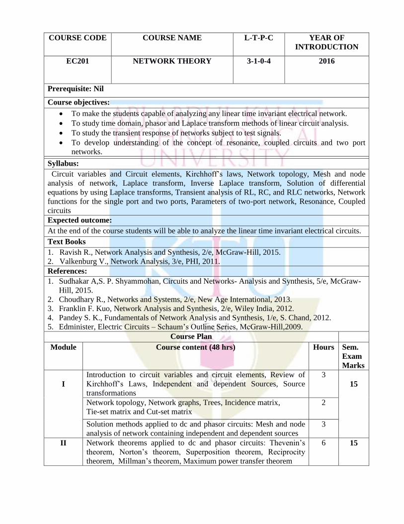
COURSE CODE COURSE NAME L-T-P-C YEAR OF
INTRODUCTION
EC201 NETWORK THEORY 3-1-0-4 2016
Prerequisite: Nil
Course objectives:
To make the students capable of analyzing any linear time invariant electrical network.
To study time domain, phasor and Laplace transform methods of linear circuit analysis.
To study the transient response of networks subject to test signals.
To develop understanding of the concept of resonance, coupled circuits and two port
networks.
Syllabus:
Circuit variables and Circuit elements, Kirchhoff’s laws, Network topology, Mesh and node
analysis of network, Laplace transform, Inverse Laplace transform, Solution of differential
equations by using Laplace transforms, Transient analysis of RL, RC, and RLC networks, Network
functions for the single port and two ports, Parameters of two-port network, Resonance, Coupled
circuits
Expected outcome:
At the end of the course students will be able to analyze the linear time invariant electrical circuits.
Text Books
1. Ravish R., Network Analysis and Synthesis, 2/e, McGraw-Hill, 2015.
2. Valkenburg V., Network Analysis, 3/e, PHI, 2011.
References:
1. Sudhakar A,S. P. Shyammohan, Circuits and Networks- Analysis and Synthesis, 5/e, McGraw-
Hill, 2015.
2. Choudhary R., Networks and Systems, 2/e, New Age International, 2013.
3. Franklin F. Kuo, Network Analysis and Synthesis, 2/e, Wiley India, 2012.
4. Pandey S. K., Fundamentals of Network Analysis and Synthesis, 1/e, S. Chand, 2012.
5. Edminister, Electric Circuits – Schaum’s Outline Series, McGraw-Hill,2009.
Course Plan
Module Course content (48 hrs) Hours Sem.
Exam
Marks
I
Introduction to circuit variables and circuit elements, Review of
Kirchhoff’s Laws, Independent and dependent Sources, Source
transformations
3
15
Network topology, Network graphs, Trees, Incidence matrix,
Tie-set matrix and Cut-set matrix
2
Solution methods applied to dc and phasor circuits: Mesh and node
analysis of network containing independent and dependent sources
3
II Network theorems applied to dc and phasor circuits: Thevenin’s
theorem, Norton’s theorem, Superposition theorem, Reciprocity
theorem, Millman’s theorem, Maximum power transfer theorem
6 15
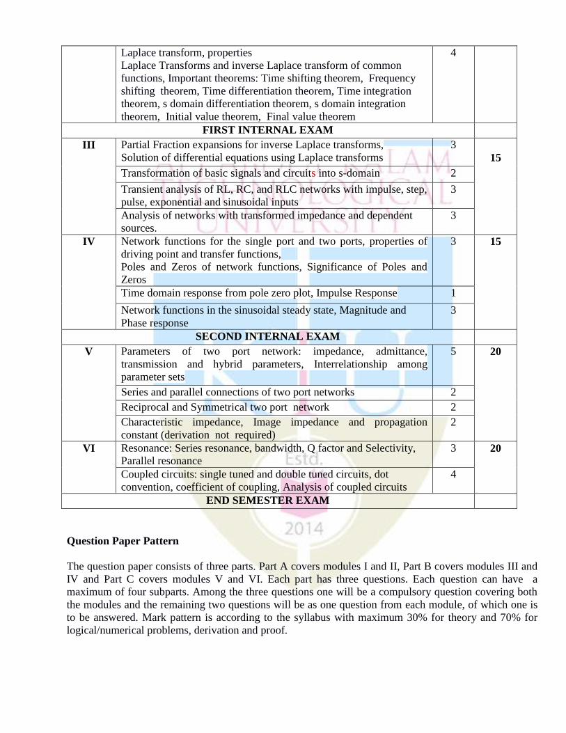
Laplace transform, properties
Laplace Transforms and inverse Laplace transform of common
functions, Important theorems: Time shifting theorem, Frequency
shifting theorem, Time differentiation theorem, Time integration
theorem, s domain differentiation theorem, s domain integration
theorem, Initial value theorem, Final value theorem
4
FIRST INTERNAL EXAM
III Partial Fraction expansions for inverse Laplace transforms,
Solution of differential equations using Laplace transforms
3
15
Transformation of basic signals and circuits into s-domain 2
Transient analysis of RL, RC, and RLC networks with impulse, step,
pulse, exponential and sinusoidal inputs
3
Analysis of networks with transformed impedance and dependent
sources.
3
IV Network functions for the single port and two ports, properties of
driving point and transfer functions,
Poles and Zeros of network functions, Significance of Poles and
Zeros
3 15
Time domain response from pole zero plot, Impulse Response 1
Network functions in the sinusoidal steady state, Magnitude and
Phase response
3
SECOND INTERNAL EXAM
V Parameters of two port network: impedance, admittance,
transmission and hybrid parameters, Interrelationship among
parameter sets
5 20
Series and parallel connections of two port networks 2
Reciprocal and Symmetrical two port network 2
Characteristic impedance, Image impedance and propagation
constant (derivation not required)
2
VI Resonance: Series resonance, bandwidth, Q factor and Selectivity,
Parallel resonance
3 20
Coupled circuits: single tuned and double tuned circuits, dot
convention, coefficient of coupling, Analysis of coupled circuits
4
END SEMESTER EXAM
Question Paper Pattern
The question paper consists of three parts. Part A covers modules I and II, Part B covers modules III and
IV and Part C covers modules V and VI. Each part has three questions. Each question can have a
maximum of four subparts. Among the three questions one will be a compulsory question covering both
the modules and the remaining two questions will be as one question from each module, of which one is
to be answered. Mark pattern is according to the syllabus with maximum 30% for theory and 70% for
logical/numerical problems, derivation and proof.
COURSE
CODE
COURSE NAME L-T-P-C YEAR OF INTRODUCTION
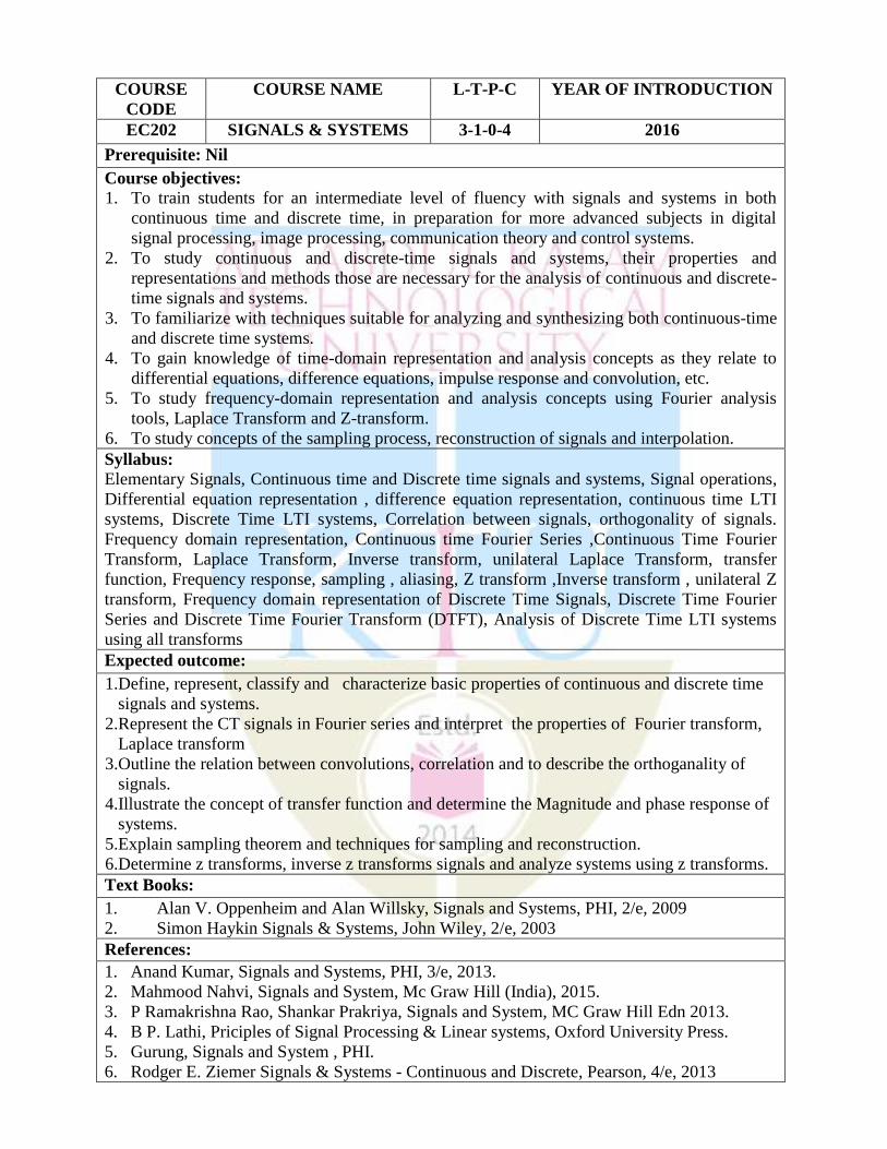
EC202 SIGNALS & SYSTEMS 3-1-0-4 2016
Prerequisite: Nil
Course objectives:
1. To train students for an intermediate level of fluency with signals and systems in both
continuous time and discrete time, in preparation for more advanced subjects in digital
signal processing, image processing, communication theory and control systems.
2. To study continuous and discrete-time signals and systems, their properties and
representations and methods those are necessary for the analysis of continuous and discrete-
time signals and systems.
3. To familiarize with techniques suitable for analyzing and synthesizing both continuous-time
and discrete time systems.
4. To gain knowledge of time-domain representation and analysis concepts as they relate to
differential equations, difference equations, impulse response and convolution, etc.
5. To study frequency-domain representation and analysis concepts using Fourier analysis
tools, Laplace Transform and Z-transform.
6. To study concepts of the sampling process, reconstruction of signals and interpolation.
Syllabus:
Elementary Signals, Continuous time and Discrete time signals and systems, Signal operations,
Differential equation representation , difference equation representation, continuous time LTI
systems, Discrete Time LTI systems, Correlation between signals, orthogonality of signals.
Frequency domain representation, Continuous time Fourier Series ,Continuous Time Fourier
Transform, Laplace Transform, Inverse transform, unilateral Laplace Transform, transfer
function, Frequency response, sampling , aliasing, Z transform ,Inverse transform , unilateral Z
transform, Frequency domain representation of Discrete Time Signals, Discrete Time Fourier
Series and Discrete Time Fourier Transform (DTFT), Analysis of Discrete Time LTI systems
using all transforms
Expected outcome:
1.Define, represent, classify and characterize basic properties of continuous and discrete time
signals and systems.
2.Represent the CT signals in Fourier series and interpret the properties of Fourier transform,
Laplace transform
3.Outline the relation between convolutions, correlation and to describe the orthoganality of
signals.
4.Illustrate the concept of transfer function and determine the Magnitude and phase response of
systems.
5.Explain sampling theorem and techniques for sampling and reconstruction.
6.Determine z transforms, inverse z transforms signals and analyze systems using z transforms.
Text Books:
1. Alan V. Oppenheim and Alan Willsky, Signals and Systems, PHI, 2/e, 2009
2. Simon Haykin Signals & Systems, John Wiley, 2/e, 2003
References:
1. Anand Kumar, Signals and Systems, PHI, 3/e, 2013.
2. Mahmood Nahvi, Signals and System, Mc Graw Hill (India), 2015.
3. P Ramakrishna Rao, Shankar Prakriya, Signals and System, MC Graw Hill Edn 2013.
4. B P. Lathi, Priciples of Signal Processing & Linear systems, Oxford University Press.
5. Gurung, Signals and System , PHI.
6. Rodger E. Ziemer Signals & Systems - Continuous and Discrete, Pearson, 4/e, 2013
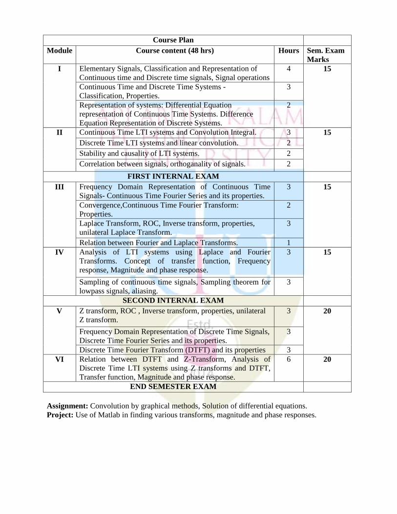
Course Plan
Module Course content (48 hrs) Hours Sem. Exam
Marks
I Elementary Signals, Classification and Representation of
Continuous time and Discrete time signals, Signal operations
4 15
Continuous Time and Discrete Time Systems -
Classification, Properties.
3
Representation of systems: Differential Equation
representation of Continuous Time Systems. Difference
Equation Representation of Discrete Systems.
2
II Continuous Time LTI systems and Convolution Integral. 3 15
Discrete Time LTI systems and linear convolution. 2
Stability and causality of LTI systems. 2
Correlation between signals, orthoganality of signals. 2
FIRST INTERNAL EXAM
III Frequency Domain Representation of Continuous Time
Signals- Continuous Time Fourier Series and its properties.
3 15
Convergence,Continuous Time Fourier Transform:
Properties.
2
Laplace Transform, ROC, Inverse transform, properties,
unilateral Laplace Transform.
3
Relation between Fourier and Laplace Transforms. 1
IV Analysis of LTI systems using Laplace and Fourier
Transforms. Concept of transfer function, Frequency
response, Magnitude and phase response.
3 15
Sampling of continuous time signals, Sampling theorem for
lowpass signals, aliasing.
3
SECOND INTERNAL EXAM
V Z transform, ROC , Inverse transform, properties, unilateral
Z transform.
3 20
Frequency Domain Representation of Discrete Time Signals,
Discrete Time Fourier Series and its properties.
3
Discrete Time Fourier Transform (DTFT) and its properties 3
VI Relation between DTFT and Z-Transform, Analysis of
Discrete Time LTI systems using Z transforms and DTFT,
Transfer function, Magnitude and phase response.
6 20
END SEMESTER EXAM
Assignment: Convolution by graphical methods, Solution of differential equations.
Project: Use of Matlab in finding various transforms, magnitude and phase responses.
Question Paper Pattern
The question paper consists of three parts. Part A covers modules I and II, Part B covers modules
III and IV and Part C covers modules V and VI. Each part has three questions. Each question can
have a maximum of four subparts. Among the three questions one will be a compulsory question
covering both the modules and the remaining two questions will be as one question from each
module, of which one is to be answered. Mark pattern is according to the syllabus with
maximum 30 % for theory and 70% for logical/numerical problems, derivation and proof.
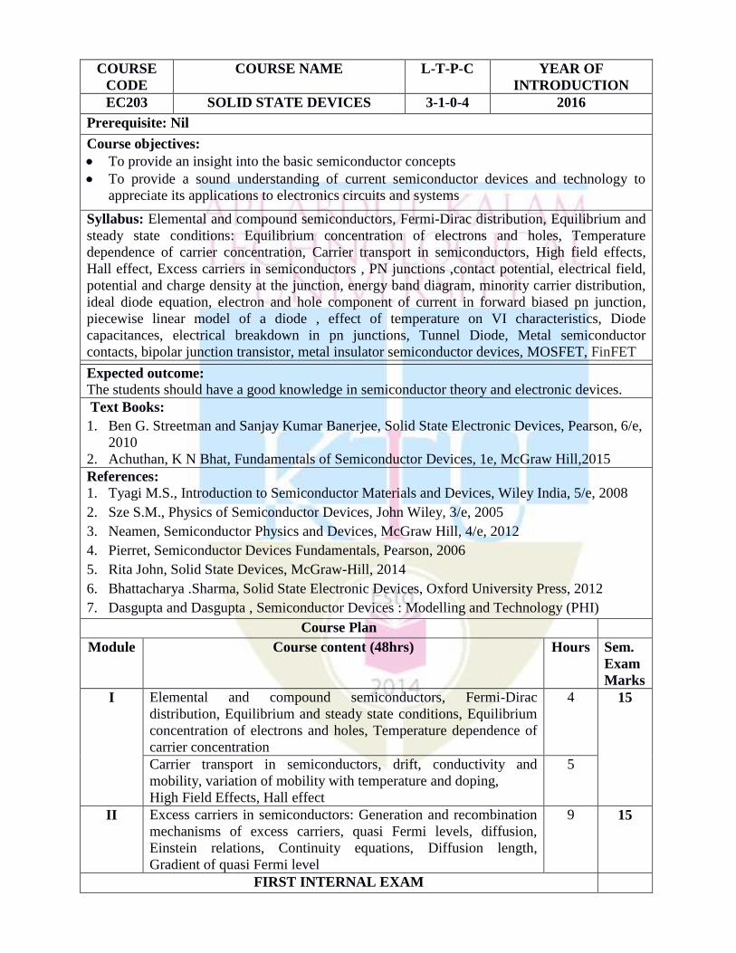
COURSE
CODE
COURSE NAME L-T-P-C YEAR OF
INTRODUCTION
EC203 SOLID STATE DEVICES 3-1-0-4 2016
Prerequisite: Nil
Course objectives:
To provide an insight into the basic semiconductor concepts
To provide a sound understanding of current semiconductor devices and technology to
appreciate its applications to electronics circuits and systems
Syllabus: Elemental and compound semiconductors, Fermi-Dirac distribution, Equilibrium and
steady state conditions: Equilibrium concentration of electrons and holes, Temperature
dependence of carrier concentration, Carrier transport in semiconductors, High field effects,
Hall effect, Excess carriers in semiconductors , PN junctions ,contact potential, electrical field,
potential and charge density at the junction, energy band diagram, minority carrier distribution,
ideal diode equation, electron and hole component of current in forward biased pn junction,
piecewise linear model of a diode , effect of temperature on VI characteristics, Diode
capacitances, electrical breakdown in pn junctions, Tunnel Diode, Metal semiconductor
contacts, bipolar junction transistor, metal insulator semiconductor devices, MOSFET, FinFET
Expected outcome: The students should have a good knowledge in semiconductor theory and electronic devices.
Text Books:
1. Ben G. Streetman and Sanjay Kumar Banerjee, Solid State Electronic Devices, Pearson, 6/e,
2010
2. Achuthan, K N Bhat, Fundamentals of Semiconductor Devices, 1e, McGraw Hill,2015
References:
1. Tyagi M.S., Introduction to Semiconductor Materials and Devices, Wiley India, 5/e, 2008
2. Sze S.M., Physics of Semiconductor Devices, John Wiley, 3/e, 2005
3. Neamen, Semiconductor Physics and Devices, McGraw Hill, 4/e, 2012
4. Pierret, Semiconductor Devices Fundamentals, Pearson, 2006
5. Rita John, Solid State Devices, McGraw-Hill, 2014
6. Bhattacharya .Sharma, Solid State Electronic Devices, Oxford University Press, 2012
7. Dasgupta and Dasgupta , Semiconductor Devices : Modelling and Technology (PHI)
Course Plan
Module Course content (48hrs) Hours Sem.
Exam
Marks
I Elemental and compound semiconductors, Fermi-Dirac
distribution, Equilibrium and steady state conditions, Equilibrium
concentration of electrons and holes, Temperature dependence of
carrier concentration
4 15
Carrier transport in semiconductors, drift, conductivity and
mobility, variation of mobility with temperature and doping,
High Field Effects, Hall effect
5
II Excess carriers in semiconductors: Generation and recombination
mechanisms of excess carriers, quasi Fermi levels, diffusion,
Einstein relations, Continuity equations, Diffusion length,
Gradient of quasi Fermi level
9 15
FIRST INTERNAL EXAM
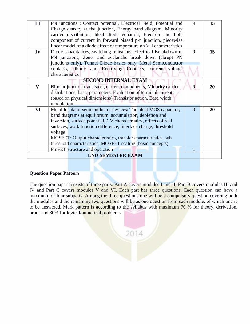
III PN junctions : Contact potential, Electrical Field, Potential and
Charge density at the junction, Energy band diagram, Minority
carrier distribution, Ideal diode equation, Electron and hole
component of current in forward biased p-n junction, piecewise
linear model of a diode effect of temperature on V-I characteristics
9 15
IV Diode capacitances, switching transients, Electrical Breakdown in
PN junctions, Zener and avalanche break down (abrupt PN
junctions only), Tunnel Diode basics only, Metal Semiconductor
contacts, Ohmic and Rectifying Contacts, current voltage
characteristics
9 15
SECOND INTERNAL EXAM
V Bipolar junction transistor , current components, Minority carrier
distributions, basic parameters, Evaluation of terminal currents
(based on physical dimensions),Transistor action, Base width
modulation
9 20
VI Metal Insulator semiconductor devices: The ideal MOS capacitor,
band diagrams at equilibrium, accumulation, depletion and
inversion, surface potential, CV characteristics, effects of real
surfaces, work function difference, interface charge, threshold
voltage
MOSFET: Output characteristics, transfer characteristics, sub
threshold characteristics, MOSFET scaling (basic concepts)
9 20
FinFET-structure and operation 1
END SEMESTER EXAM
Question Paper Pattern
The question paper consists of three parts. Part A covers modules I and II, Part B covers modules III and
IV and Part C covers modules V and VI. Each part has three questions. Each question can have a
maximum of four subparts. Among the three questions one will be a compulsory question covering both
the modules and the remaining two questions will be as one question from each module, of which one is
to be answered. Mark pattern is according to the syllabus with maximum 70 % for theory, derivation,
proof and 30% for logical/numerical problems.
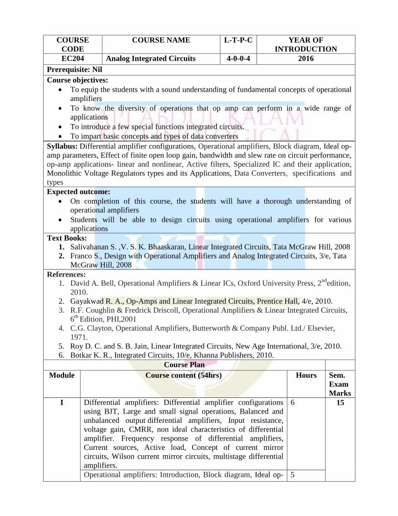
COURSE
CODE
COURSE NAME L-T-P-C YEAR OF
INTRODUCTION
EC204 Analog Integrated Circuits 4-0-0-4 2016
Prerequisite: Nil
Course objectives:
To equip the students with a sound understanding of fundamental concepts of operational
amplifiers
To know the diversity of operations that op amp can perform in a wide range of
applications
To introduce a few special functions integrated circuits.
To impart basic concepts and types of data converters
Syllabus: Differential amplifier configurations, Operational amplifiers, Block diagram, Ideal op-
amp parameters, Effect of finite open loop gain, bandwidth and slew rate on circuit performance,
op-amp applications- linear and nonlinear, Active filters, Specialized IC and their application,
Monolithic Voltage Regulators types and its Applications, Data Converters, specifications and
types
Expected outcome:
On completion of this course, the students will have a thorough understanding of
operational amplifiers
Students will be able to design circuits using operational amplifiers for various
applications
Text Books:
1. Salivahanan S. ,V. S. K. Bhaaskaran, Linear Integrated Circuits, Tata McGraw Hill, 2008
2. Franco S., Design with Operational Amplifiers and Analog Integrated Circuits, 3/e, Tata
McGraw Hill, 2008
References:
1. David A. Bell, Operational Amplifiers & Linear ICs, Oxford University Press, 2nd
edition,
2010.
2. Gayakwad R. A., Op-Amps and Linear Integrated Circuits, Prentice Hall, 4/e, 2010.
3. R.F. Coughlin & Fredrick Driscoll, Operational Amplifiers & Linear Integrated Circuits,
6th
Edition, PHI,2001
4. C.G. Clayton, Operational Amplifiers, Butterworth & Company Publ. Ltd./ Elsevier,
1971.
5. Roy D. C. and S. B. Jain, Linear Integrated Circuits, New Age International, 3/e, 2010.
6. Botkar K. R., Integrated Circuits, 10/e, Khanna Publishers, 2010.
Course Plan
Module Course content (54hrs) Hours Sem.
Exam
Marks
I Differential amplifiers: Differential amplifier configurations
using BJT, Large and small signal operations, Balanced and
unbalanced output differential amplifiers, Input resistance,
voltage gain, CMRR, non ideal characteristics of differential
amplifier. Frequency response of differential amplifiers,
Current sources, Active load, Concept of current mirror
circuits, Wilson current mirror circuits, multistage differential
amplifiers.
6 15
Operational amplifiers: Introduction, Block diagram, Ideal op- 5
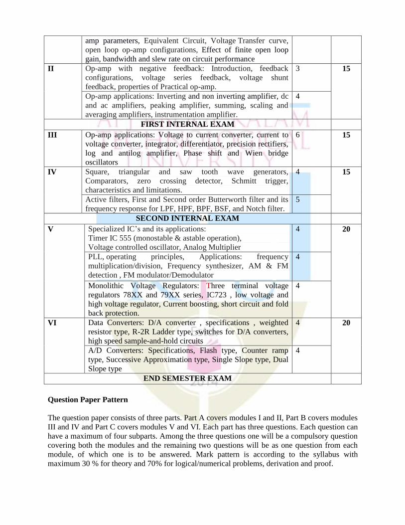
amp parameters, Equivalent Circuit, Voltage Transfer curve,
open loop op-amp configurations, Effect of finite open loop
gain, bandwidth and slew rate on circuit performance
II Op-amp with negative feedback: Introduction, feedback
configurations, voltage series feedback, voltage shunt
feedback, properties of Practical op-amp.
3 15
Op-amp applications: Inverting and non inverting amplifier, dc
and ac amplifiers, peaking amplifier, summing, scaling and
averaging amplifiers, instrumentation amplifier.
4
FIRST INTERNAL EXAM
III Op-amp applications: Voltage to current converter, current to
voltage converter, integrator, differentiator, precision rectifiers,
log and antilog amplifier, Phase shift and Wien bridge
oscillators
6 15
IV Square, triangular and saw tooth wave generators,
Comparators, zero crossing detector, Schmitt trigger,
characteristics and limitations.
4 15
Active filters, First and Second order Butterworth filter and its
frequency response for LPF, HPF, BPF, BSF, and Notch filter.
5
SECOND INTERNAL EXAM
V Specialized IC’s and its applications:
Timer IC 555 (monostable & astable operation),
Voltage controlled oscillator, Analog Multiplier
4 20
PLL, operating principles, Applications: frequency
multiplication/division, Frequency synthesizer, AM & FM
detection , FM modulator/Demodulator
4
Monolithic Voltage Regulators: Three terminal voltage
regulators 78XX and 79XX series, IC723 , low voltage and
high voltage regulator, Current boosting, short circuit and fold
back protection.
4
VI Data Converters: D/A converter , specifications , weighted
resistor type, R-2R Ladder type, switches for D/A converters,
high speed sample-and-hold circuits
4 20
A/D Converters: Specifications, Flash type, Counter ramp
type, Successive Approximation type, Single Slope type, Dual
Slope type
4
END SEMESTER EXAM
Question Paper Pattern
The question paper consists of three parts. Part A covers modules I and II, Part B covers modules
III and IV and Part C covers modules V and VI. Each part has three questions. Each question can
have a maximum of four subparts. Among the three questions one will be a compulsory question
covering both the modules and the remaining two questions will be as one question from each
module, of which one is to be answered. Mark pattern is according to the syllabus with
maximum 30 % for theory and 70% for logical/numerical problems, derivation and proof.
COURSE
CODE
COURSE NAME L-T-P-
C
YEAR OF
INTRODUCTION
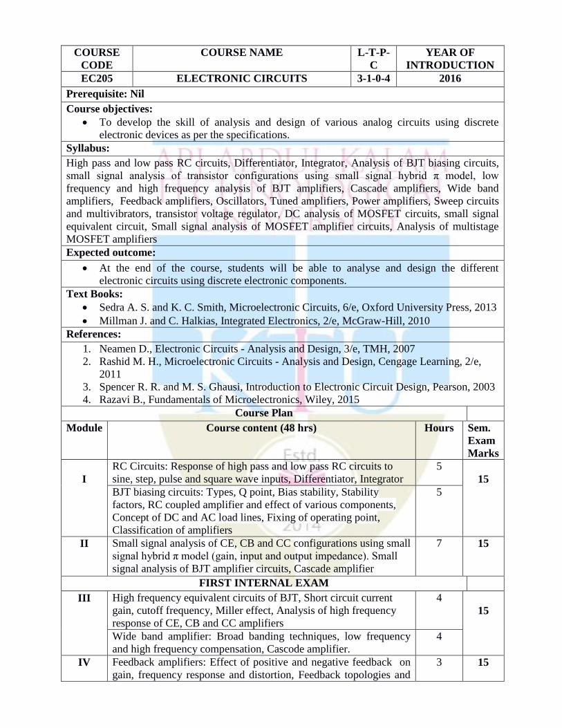
EC205 ELECTRONIC CIRCUITS 3-1-0-4 2016
Prerequisite: Nil
Course objectives:
To develop the skill of analysis and design of various analog circuits using discrete
electronic devices as per the specifications.
Syllabus:
High pass and low pass RC circuits, Differentiator, Integrator, Analysis of BJT biasing circuits,
small signal analysis of transistor configurations using small signal hybrid π model, low
frequency and high frequency analysis of BJT amplifiers, Cascade amplifiers, Wide band
amplifiers, Feedback amplifiers, Oscillators, Tuned amplifiers, Power amplifiers, Sweep circuits
and multivibrators, transistor voltage regulator, DC analysis of MOSFET circuits, small signal
equivalent circuit, Small signal analysis of MOSFET amplifier circuits, Analysis of multistage
MOSFET amplifiers
Expected outcome:
At the end of the course, students will be able to analyse and design the different
electronic circuits using discrete electronic components.
Text Books:
Sedra A. S. and K. C. Smith, Microelectronic Circuits, 6/e, Oxford University Press, 2013
Millman J. and C. Halkias, Integrated Electronics, 2/e, McGraw-Hill, 2010
References:
1. Neamen D., Electronic Circuits - Analysis and Design, 3/e, TMH, 2007
2. Rashid M. H., Microelectronic Circuits - Analysis and Design, Cengage Learning, 2/e,
2011
3. Spencer R. R. and M. S. Ghausi, Introduction to Electronic Circuit Design, Pearson, 2003
4. Razavi B., Fundamentals of Microelectronics, Wiley, 2015
Course Plan
Module Course content (48 hrs) Hours Sem.
Exam
Marks
I
RC Circuits: Response of high pass and low pass RC circuits to
sine, step, pulse and square wave inputs, Differentiator, Integrator
5
15
BJT biasing circuits: Types, Q point, Bias stability, Stability
factors, RC coupled amplifier and effect of various components,
Concept of DC and AC load lines, Fixing of operating point,
Classification of amplifiers
5
II
Small signal analysis of CE, CB and CC configurations using small
signal hybrid π model (gain, input and output impedance). Small
signal analysis of BJT amplifier circuits, Cascade amplifier
7 15
FIRST INTERNAL EXAM
III High frequency equivalent circuits of BJT, Short circuit current
gain, cutoff frequency, Miller effect, Analysis of high frequency
response of CE, CB and CC amplifiers
4
15
Wide band amplifier: Broad banding techniques, low frequency
and high frequency compensation, Cascode amplifier.
4
IV Feedback amplifiers: Effect of positive and negative feedback on
gain, frequency response and distortion, Feedback topologies and
3 15
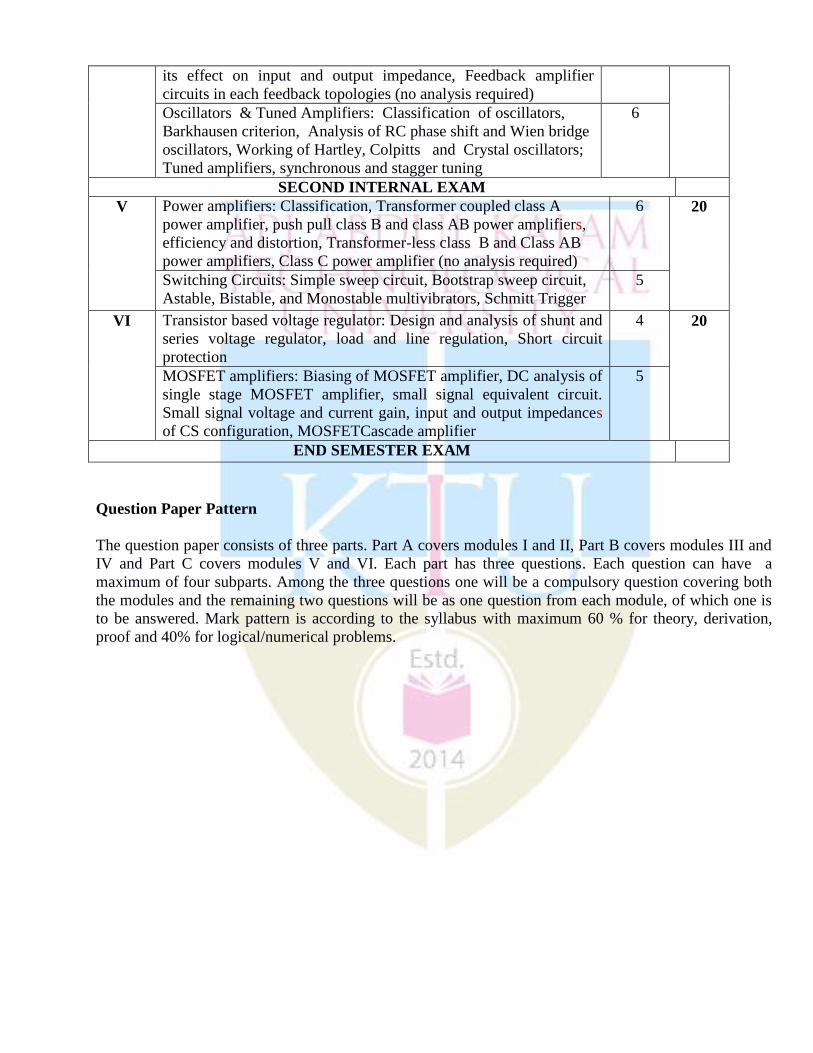
its effect on input and output impedance, Feedback amplifier
circuits in each feedback topologies (no analysis required)
Oscillators & Tuned Amplifiers: Classification of oscillators,
Barkhausen criterion, Analysis of RC phase shift and Wien bridge
oscillators, Working of Hartley, Colpitts and Crystal oscillators;
Tuned amplifiers, synchronous and stagger tuning
6
SECOND INTERNAL EXAM
V Power amplifiers: Classification, Transformer coupled class A
power amplifier, push pull class B and class AB power amplifiers,
efficiency and distortion, Transformer-less class B and Class AB
power amplifiers, Class C power amplifier (no analysis required)
6 20
Switching Circuits: Simple sweep circuit, Bootstrap sweep circuit,
Astable, Bistable, and Monostable multivibrators, Schmitt Trigger
5
VI Transistor based voltage regulator: Design and analysis of shunt and
series voltage regulator, load and line regulation, Short circuit
protection
4 20
MOSFET amplifiers: Biasing of MOSFET amplifier, DC analysis of
single stage MOSFET amplifier, small signal equivalent circuit.
Small signal voltage and current gain, input and output impedances
of CS configuration, MOSFETCascade amplifier
5
END SEMESTER EXAM
Question Paper Pattern
The question paper consists of three parts. Part A covers modules I and II, Part B covers modules III and
IV and Part C covers modules V and VI. Each part has three questions. Each question can have a
maximum of four subparts. Among the three questions one will be a compulsory question covering both
the modules and the remaining two questions will be as one question from each module, of which one is
to be answered. Mark pattern is according to the syllabus with maximum 60 % for theory, derivation,
proof and 40% for logical/numerical problems.
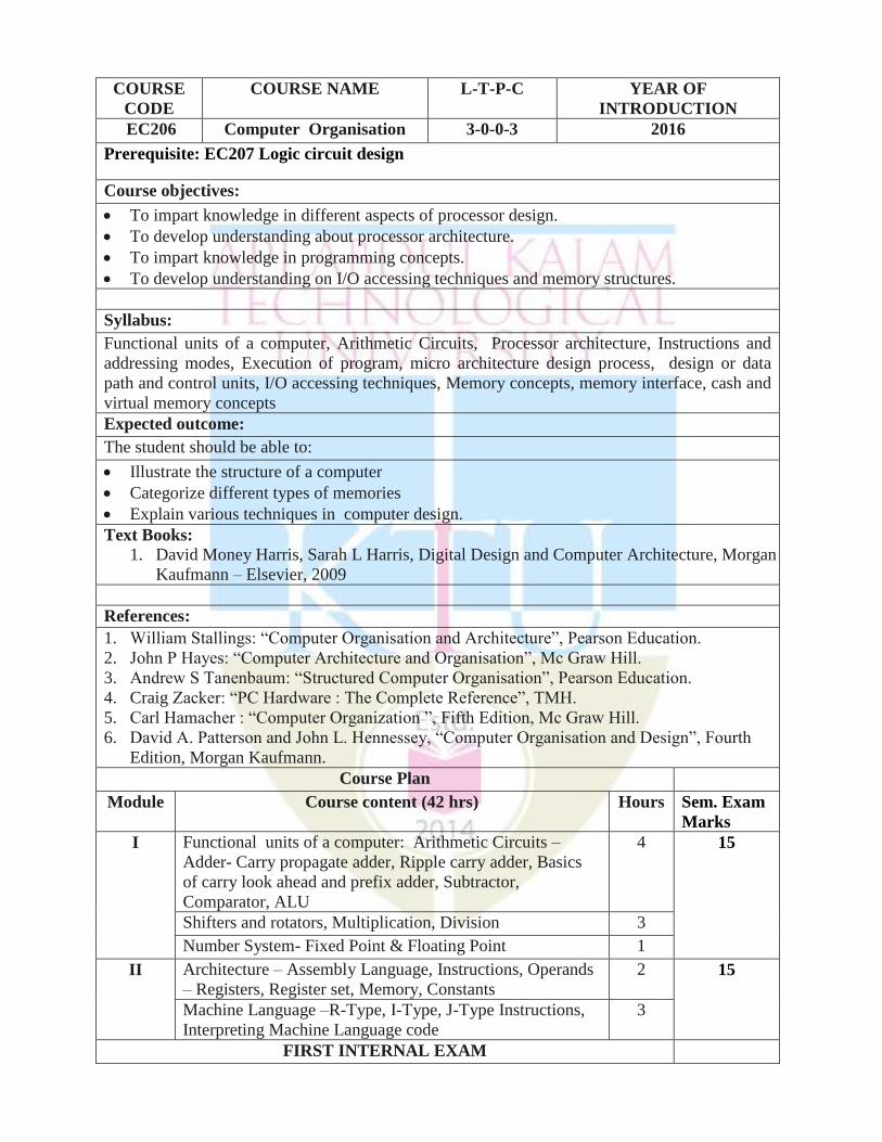
COURSE
CODE
COURSE NAME L-T-P-C YEAR OF
INTRODUCTION
EC206 Computer Organisation 3-0-0-3 2016
Prerequisite: EC207 Logic circuit design
Course objectives:
To impart knowledge in different aspects of processor design.
To develop understanding about processor architecture.
To impart knowledge in programming concepts.
To develop understanding on I/O accessing techniques and memory structures.
Syllabus:
Functional units of a computer, Arithmetic Circuits, Processor architecture, Instructions and
addressing modes, Execution of program, micro architecture design process, design or data
path and control units, I/O accessing techniques, Memory concepts, memory interface, cash and
virtual memory concepts
Expected outcome:
The student should be able to:
Illustrate the structure of a computer
Categorize different types of memories
Explain various techniques in computer design.
Text Books:
1. David Money Harris, Sarah L Harris, Digital Design and Computer Architecture, Morgan
Kaufmann – Elsevier, 2009
References:
1. William Stallings: “Computer Organisation and Architecture”, Pearson Education.
2. John P Hayes: “Computer Architecture and Organisation”, Mc Graw Hill.
3. Andrew S Tanenbaum: “Structured Computer Organisation”, Pearson Education.
4. Craig Zacker: “PC Hardware : The Complete Reference”, TMH.
5. Carl Hamacher : “Computer Organization ”, Fifth Edition, Mc Graw Hill.
6. David A. Patterson and John L. Hennessey, “Computer Organisation and Design”, Fourth
Edition, Morgan Kaufmann.
Course Plan
Module Course content (42 hrs) Hours Sem. Exam
Marks
I Functional units of a computer: Arithmetic Circuits –
Adder- Carry propagate adder, Ripple carry adder, Basics
of carry look ahead and prefix adder, Subtractor,
Comparator, ALU
4 15
Shifters and rotators, Multiplication, Division 3
Number System- Fixed Point & Floating Point 1
II Architecture – Assembly Language, Instructions, Operands
– Registers, Register set, Memory, Constants
2 15
Machine Language –R-Type, I-Type, J-Type Instructions,
Interpreting Machine Language code
3
FIRST INTERNAL EXAM
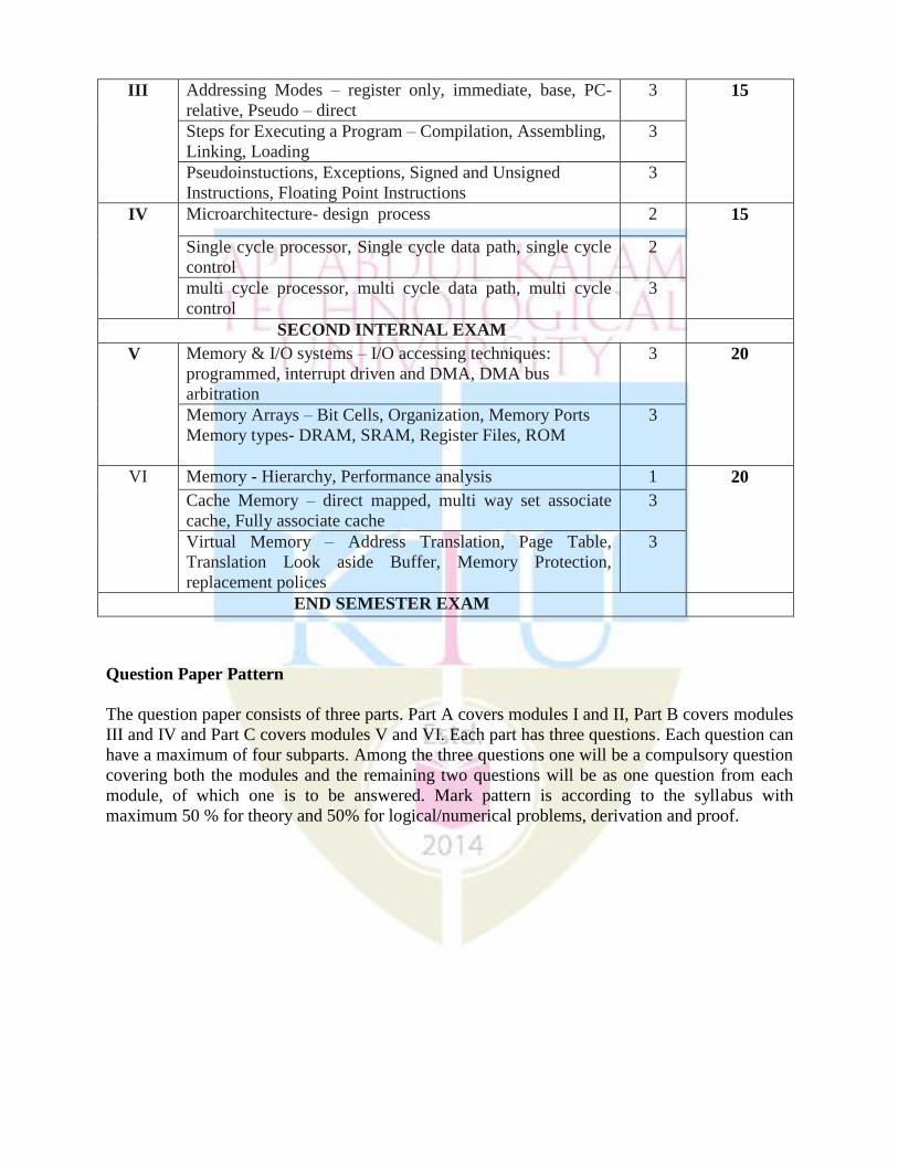
III Addressing Modes – register only, immediate, base, PC-
relative, Pseudo – direct
3 15
Steps for Executing a Program – Compilation, Assembling,
Linking, Loading
3
Pseudoinstuctions, Exceptions, Signed and Unsigned
Instructions, Floating Point Instructions
3
IV Microarchitecture- design process 2 15
Single cycle processor, Single cycle data path, single cycle
control
2
multi cycle processor, multi cycle data path, multi cycle
control
3
SECOND INTERNAL EXAM
V Memory & I/O systems – I/O accessing techniques:
programmed, interrupt driven and DMA, DMA bus
arbitration
3 20
Memory Arrays – Bit Cells, Organization, Memory Ports
Memory types- DRAM, SRAM, Register Files, ROM
3
VI Memory - Hierarchy, Performance analysis 1 20
Cache Memory – direct mapped, multi way set associate
cache, Fully associate cache
3
Virtual Memory – Address Translation, Page Table,
Translation Look aside Buffer, Memory Protection,
replacement polices
3
END SEMESTER EXAM
Question Paper Pattern
The question paper consists of three parts. Part A covers modules I and II, Part B covers modules
III and IV and Part C covers modules V and VI. Each part has three questions. Each question can
have a maximum of four subparts. Among the three questions one will be a compulsory question
covering both the modules and the remaining two questions will be as one question from each
module, of which one is to be answered. Mark pattern is according to the syllabus with
maximum 50 % for theory and 50% for logical/numerical problems, derivation and proof.
COURSE
CODE
COURSE NAME L-T-P-C YEAR OF
INTRODUCTION
EC207 LOGIC CIRCUIT DESIGN 3-0-0-3 2016
Prerequisite:Nil
Course objectives:
To work with a positional number systems and numeric representations
To introduce basic postulates of Boolean algebra and show the correlation between Boolean
expression
To outline the formal procedures for the analysis and design of combinational circuits and
sequential circuits
To study the fundamentals of HDL
To design and implement combinational circuits using basic programmable blocks
To design and implement synchronous sequential circuits
Syllabus:
Positional Number Systems, Boolean algebra, Combinational Logic, HDL concepts ,Digital ICs,
Programmable Logic Devices, Sequential Logic, Sequential Circuits
Expected outcome:
The student should able to:
1. Compare various positional number systems and binary codes
2. Apply Boolean algebra in logic circuit design
3. Design combinational and sequential circuits
4. Design and implement digital systems using basic programmable blocks
5. Formulate various digital systems using HDL
Text Books:
1. Donald D Givone, Digital Principles and Design, Tata McGraw Hill, 2003
2. John F Wakerly, Digital Design Principles and Practices, Pearson Prentice Hall, 2007
References: 1.Ronald J Tocci, Digital Systems, Pearson Education, 11
th edition,2010
2.Thomas L Floyd, Digital Fundamentals, Pearson Education, 8th
edition 2009
3.Moris Mano, Digital Design, Prentice Hall of India, 3rd
edition, 2002
4.John M Yarbrough, Digital Logic Applications and Design, Cenage learning, 2009
5.David Money Harris, Sarah L Harris, Digital Design and Computer Architecture, Morgan
Kaufmann – Elsevier, 2009
Course Plan
Modul
e
Course content (42 hrs) Hours Sem.
Exam
Marks
I Number systems- decimal, binary, octal, hexa decimal, base conversion 2 15
1’s and 2’s complement, signed number representation
Binary arithmetic, binary subtraction using 2’s complement
2
Binary codes (grey, BCD and Excess-3), Error detection and correcting
codes : Parity(odd, even), Hamming code (7,4), Alphanumeric codes :
ASCII
2
II Logic expressions, Boolean laws, Duality, De Morgan's law, Logic
functions and gates
2 15
Canonical forms: SOP, POS, Realisation of logic expressions using K- 2
map (2,3,4 variables)
Design of combinational circuits – adder, subtractor, 4 bit
adder/subtractor, BCD adder, MUX, DEMUX, Decoder,BCD to 7
segment decoder, Encoder, Priority encoder, Comparator (2/3 bits)
4
FIRST INTERNAL EXAM
III Introduction to HDL : Logic descriptions using HDL, basics of
modeling (only for assignments) 2 0
Logic families and its characteristics: Logic levels, propagation delay,
fan in, fan out, noise immunity , power dissipation, TTL subfamilies
1 15
NAND in TTL (totem pole, open collector and tri-state),
CMOS:NAND, NOR, and NOT in CMOS, Comparison of logic
families (TTL,ECL,CMOS) in terms of fan-in, fan-out, supply voltage,
propagation delay, logic voltage and current levels, power dissipation
and noise margin
2
Programmable Logic devices - ROM, PLA, PAL, implementation of
simple circuits using PLA
2
IV Sequential circuits - latch, flip flop ( SR, JK, T, D), master slave JK FF,
conversion of FFs, excitation table and characteristic equations
3 15
Asynchronous and synchronous counter design, mod N counters,
random sequence generator
5
SECOND INTERNAL EXAM
V Shift Registers - SIPO, SISO, PISO, PIPO, Shift registers with parallel
LOAD/SHIFT
Shift register counter - Ring Counter and Johnson Counter
3 20
Mealy and Moore models, state machine ,notations, state diagram, state
table, transition table, excitation table, state equations
3
VI Construction of state diagram – up down counter, sequence detector 3 20
Synchronous sequential circuit design - State equivalence 2
State reduction – equivalence classes, implication chart 2
END SEMESTER EXAM
Assignments:
1. Simple combinational circuit design using MUX,DEMUX, PLA & PAL
2. HDL simulation of circuits like simple ALU, up-down counter, linear feedback shift register,
sequence generator
Question Paper Pattern
The question paper consists of three parts. Part A covers modules I and II, Part B covers modules III and
IV and Part C covers modules V and VI. Each part has three questions. Each question have a maximum
of four subparts. Among the three questions one will be a compulsory question covering both the
modules and the remaining two questions will be as one question from each module, of which one is to
be answered. Mark pattern is according to the syllabus with maximum 50 % for theory, derivation, proof
and 50% for logical/numerical problems.
COURSE
CODE
COURSE NAME L-T-P-C YEAR OF
INTRODUCTION
EC208 ANALOG COMMUNICATION
ENGINEERING
3-0-0-3 2016
Prerequisite: EC205 Electronic circuits
Course objectives:
To study the concepts and types of modulation schemes.
To study different types of radio transmitters and receivers.
To study the effects of noise in analog communication systems
Syllabus: Elements of communication system, Need for modulation, amplitude Modulation, amplitude
modulator circuit, demodulator circuit, AM transmitters, Types of AM, AM Receiver, Angle
modulation: principles of frequency modulation, phase modulation, frequency modulator
circuits, FM transmitters, FM receiver, Noise in communication system, Effect of noise in
Analog Communication Systems, Telephone systems, standard telephone set, cordless
telephones .
Expected outcome:
Student will understand the fundamentals ideas of noises and its effect in communication
system.
Students can explain the principle and working of AM, FM, and PM system and transmitters
and receivers.
Students will be able to know the basic ideas of PSTN and advanced line communication
systems.
Text Books:
1. Simon Haykin, Communication Systems, Wiley 4/e, 2006.
2. Tomasi, Electronic Communications System, Pearson, 5/e,2011.
References:
3. Dennis Roody and John Coolen, Electronic Communication, Pearson, 4/e, 2011.
4. Tomasi,Advanced Electronic Communications Systems, Pearson, 6/e, 2012.
5. Taub ,Schilling, Saha,Principles of communication system,McGraw Hill,2013.
6. George Kennedy, ElectronicCommunication Systems, McGrawHill, 4/e, 2008.
7. Blake, Electronic Communication system, Cengage, 2/e , 2012.
Course Plan
Module Course content (42 hrs) Hours Sem.
Exam
Marks
I Introduction, elements of communication system, time and
frequency domains, Need for modulation
2 15
Noise in communication system, shot noise, thermal noise,
white noise, partition noise, flicker noise, burst noise, signal to
noise ratio, noise figure, noise temperature, narrow band
noise, representation in terms of in-phase and quadrature
components, envelope and phase components, sine wave plus
narrow band noise.
5
II Amplitude modulation: Sinusoidal AM modulation index, Average
power, Effective voltage and current, Nonsinusoidal modulation 4
Amplitude modulator circuits, Amplitude demodulator circuit, 3
AM transmitters
FIRST INTERNAL EXAM
III AM Receiver, super heterodyne receiver, detector, tuning
range, tracking, sensitivity and gain, Image rejection, double
conversion, adjacent channel rejection, Automatic Gain
Control (AGC).
4 15
Single Sideband Modulation,Principles, Balanced Modulators,
Singly & Doubly Balanced Modulators, SSB Generation, Filter
Method, Phasing Method & Third Method, SSB Reception,
Modified SSB Systems , Pilot Carrier SSB & ISB, Companded
SSB.
5
IV Angle modulation: Frequency modulation, Sinusoidal FM, Frequency spectrum,
modulation index ,average power, Non-sinusoidal modulation,
deviation ratio, comparison of AM and FM
3 15
Phase modulation, Equivalence between PM and FM,
Sinusoidal Phase Modulation, Digital Phase Modulation.
3
SECOND INTERNAL EXAM
Angle modulator Circuits : Varactor Diode Modulators, Transistors
Modulators,
FM Transmitters: Direct & Indirect Methods.
2
V FM receiver, slope detector, balanced slope detector, Foster-
Seeley discriminator, Ratio Detector, Quadrature detector, PLL
demodulator, Automatic Frequency Control, Amplitude limiters,
Pre-emphasis and De-emphasis,
3 20
Effect of noise in analog communication Systems- AM
Systems, DSBSC AM, SSB AM, Angle modulation,
Threshold Effect in Angle modulation.
4
VI Telephone systems, standard telephone set, basic call
procedures and tones, DTMF, cordless telephones.
4
END SEMESTER EXAM
Assignment
Study of
1. The telephone circuit - Local subscriber loop, Private-line circuits, Voice-frequency circuit
arrangements.
2. The public telephone network - Instruments, Local loops, Trunk circuits and exchanges,
Local central office Exchanges, Automated central office switches and Exchanges.
Question Paper Pattern
The question paper consists of three parts. Part A covers modules I and II, Part B covers modules
III and IV and Part C covers modules V and VI. Each part has three questions. Each question can
have a maximum of four subparts. Among the three questions one will be a compulsory question
covering both the modules and the remaining two questions will be as one question from each
module, of which one is to be answered. Mark pattern is according to the syllabus with
maximum 30 % for theory and 70% for logical/numerical problems, derivation and proof.
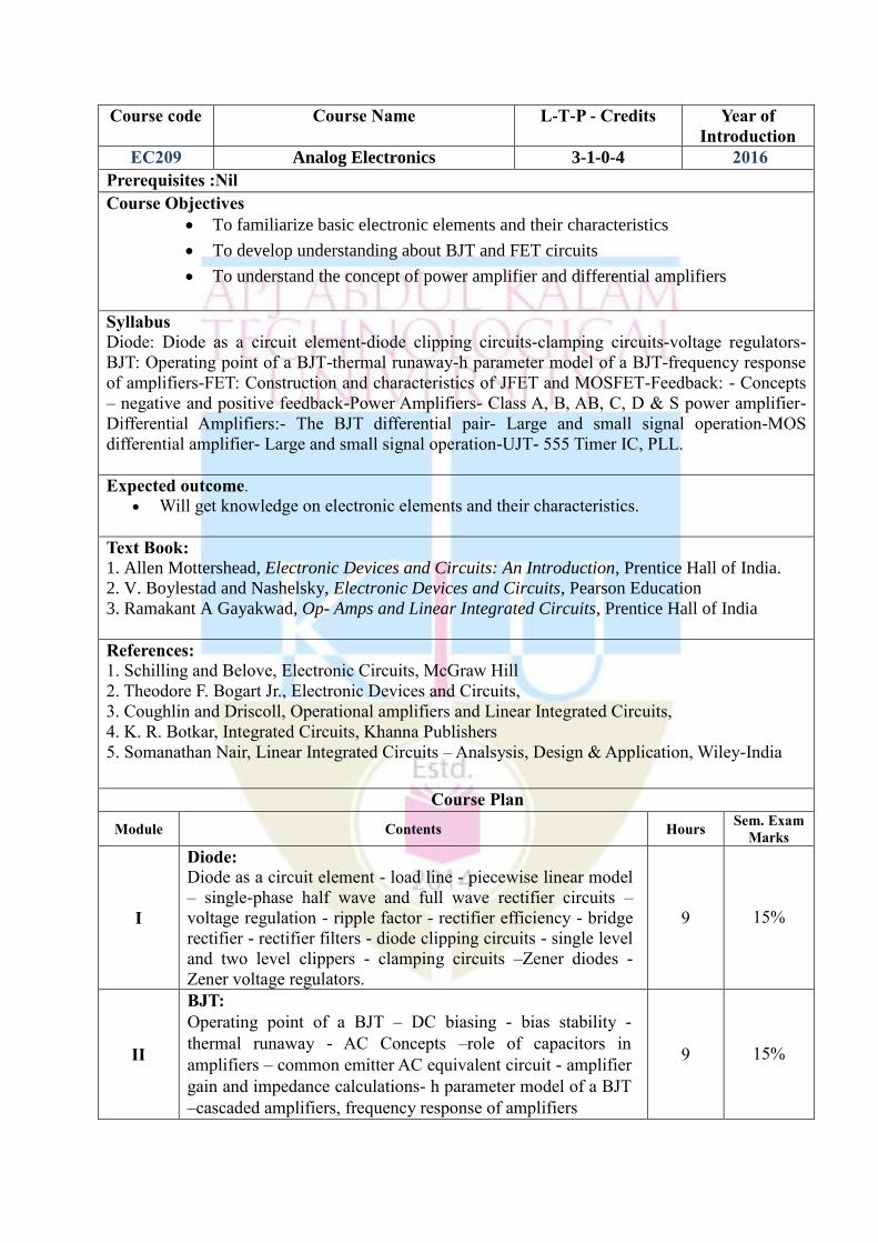
Course code Course Name L-T-P - Credits Year of
Introduction
EC209 Analog Electronics 3-1-0-4 2016
Prerequisites :Nil
Course Objectives
To familiarize basic electronic elements and their characteristics
To develop understanding about BJT and FET circuits
To understand the concept of power amplifier and differential amplifiers
Syllabus
Diode: Diode as a circuit element-diode clipping circuits-clamping circuits-voltage regulators-
BJT: Operating point of a BJT-thermal runaway-h parameter model of a BJT-frequency response
of amplifiers-FET: Construction and characteristics of JFET and MOSFET-Feedback: - Concepts
– negative and positive feedback-Power Amplifiers- Class A, B, AB, C, D & S power amplifier-
Differential Amplifiers:- The BJT differential pair- Large and small signal operation-MOS
differential amplifier- Large and small signal operation-UJT- 555 Timer IC, PLL.
Expected outcome.
Will get knowledge on electronic elements and their characteristics.
Text Book:
1. Allen Mottershead, Electronic Devices and Circuits: An Introduction, Prentice Hall of India.
2. V. Boylestad and Nashelsky, Electronic Devices and Circuits, Pearson Education
3. Ramakant A Gayakwad, Op- Amps and Linear Integrated Circuits, Prentice Hall of India
References:
1. Schilling and Belove, Electronic Circuits, McGraw Hill
2. Theodore F. Bogart Jr., Electronic Devices and Circuits,
3. Coughlin and Driscoll, Operational amplifiers and Linear Integrated Circuits,
4. K. R. Botkar, Integrated Circuits, Khanna Publishers
5. Somanathan Nair, Linear Integrated Circuits – Analsysis, Design & Application, Wiley-India
Course Plan
Module Contents Hours Sem. Exam
Marks
I
Diode:
Diode as a circuit element - load line - piecewise linear model
– single-phase half wave and full wave rectifier circuits –
voltage regulation - ripple factor - rectifier efficiency - bridge
rectifier - rectifier filters - diode clipping circuits - single level
and two level clippers - clamping circuits –Zener diodes -
Zener voltage regulators.
9 15%
II
BJT:
Operating point of a BJT – DC biasing - bias stability -
thermal runaway - AC Concepts –role of capacitors in
amplifiers – common emitter AC equivalent circuit - amplifier
gain and impedance calculations- h parameter model of a BJT
–cascaded amplifiers, frequency response of amplifiers
9 15%
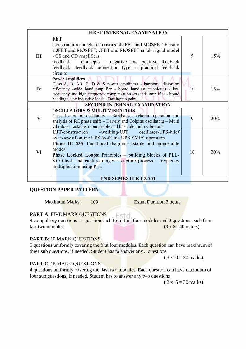
FIRST INTERNAL EXAMINATION
III
FET
Construction and characteristics of JFET and MOSFET, biasing
a JFET and MOSFET, JFET and MOSFET small signal model
- CS and CD amplifiers.
feedback: - Concepts – negative and positive feedback
feedback -feedback connection types - practical feedback
circuits
9 15%
IV
Power Amplifiers
Class A, B, AB, C, D & S power amplifiers - harmonic distortion
efficiency -wide band amplifier - broad banding techniques - low
frequency and high frequency compensation -cascode amplifier - broad
banding using inductive loads - Darlington pairs.
10 15%
SECOND INTERNAL EXAMINATION
V
OSCILLATORS & MULTI VIBRATORS
Classification of oscillators – Barkhausen criteria- operation and
analysis of RC phase shift – Hartely and Colpitts oscillators – Multi
vibrators – astable, mono stable and bi stable multi vibrators
9 20%
VI
UJT-construction –working-UJT oscillator-UPS-brief
overview of online UPS &off line UPS-SMPS-operation
Timer IC 555: Functional diagram- astable and monostable
modes
Phase Locked Loops: Principles – building blocks of PLL-
VCO-lock and capture ranges - capture process - frequency
multiplication using PLL
10 20%
END SEMESTER EXAM
QUESTION PAPER PATTERN
Maximum Marks : 100 Exam Duration:3 hours
PART A: FIVE MARK QUESTIONS
8 compulsory questions –1 question each from first four modules and 2 questions each from
last two modules (8 x 5= 40 marks)
PART B: 10 MARK QUESTIONS
5 questions uniformly covering the first four modules. Each question can have maximum of
three sub questions, if needed. Student has to answer any 3 questions
( 3 x10 = 30 marks)
PART C: 15 MARK QUESTIONS
4 questions uniformly covering the last two modules. Each question can have maximum of
four sub questions, if needed. Student has to answer any two questions
( 2 x15 = 30 marks)
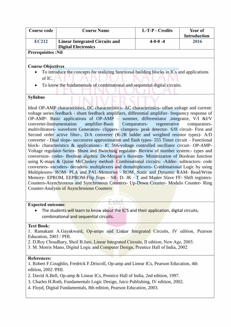
Course code Course Name L-T-P - Credits Year of
Introduction
EC212 Linear Integrated Circuits and
Digital Electronics
4-0-0 -4 2016
Prerequisites :Nil
Course Objectives
To introduce the concepts for realizing functional building blocks in ICs and applications
of IC.
To know the fundamentals of combinational and sequential digital circuits.
Syllabus
Ideal OP-AMP characteristics, DC characteristics- AC characteristics- offset voltage and current:
voltage series feedback - shunt feedback amplifiers, differential amplifier- frequency response of
OP-AMP- Basic applications of OP-AMP – summer, differentiator ,integrator, V/I &I/V
converter-Instrumentation amplifier-Basic Comparators- regenerative comparators-
multivibrators- waveform Generators- clippers- clampers- peak detector- S/H circuit- First and
Second order active filter-, D/A converter (R-2R ladder and weighted resistor types)- A/D
converter - Dual slope- successive approximation and flash types- 555 Timer circuit – Functional
block- characteristics & applications:- IC 566-voltage controlled oscillator circuit- OP-AMP-
Voltage regulator-Series- Shunt and Switching regulator- Review of number system:- types and
conversion- codes- Boolean algebra: De-Morgan’s theorem- Minimization of Boolean function
using K-maps & Quine McCluskey method- Combinational circuits: -Adder- subtractors- code
converters- encoders- decoders- multiplexers and demultiplexers- Combinational Logic by using
Multiplexers- ROM- PLA and PAL-Memories - ROM, Static and Dynamic RAM- Read/Write
Memory- EPROM, EEPROM-Flip flops – SR- D- JK - T and Master Slave FF- Shift registers-
Counters-Asynchronous and Synchronous Counters- Up-Down Counter- Modulo Counter- Ring
Counter-Analysis of Asynchronous Counters
Expected outcome:
The students will learn to know about the IC'S and their application, digital circuits,
combinational and sequential circuits.
Text Book:
1. Ramakant A.Gayakward, Op-amps and Linear Integrated Circuits, IV edition, Pearson
Education, 2003 / PHI.
2. D.Roy Choudhary, Sheil B.Jani, Linear Integrated Circuits, II edition, New Age, 2003.
3. M. Morris Mano, Digital Logic and Computer Design, Prentice Hall of India, 2002
References:
1. Robert F.Coughlin, Fredrick F.Driscoll, Op-amp and Linear ICs, Pearson Education, 4th
edition, 2002 /PHI.
2. David A.Bell, Op-amp & Linear ICs, Prentice Hall of India, 2nd edition, 1997.
3. Charles H.Roth, Fundamentals Logic Design, Jaico Publishing, IV edition, 2002.
4. Floyd, Digital Fundamentals, 8th edition, Pearson Education, 2003.
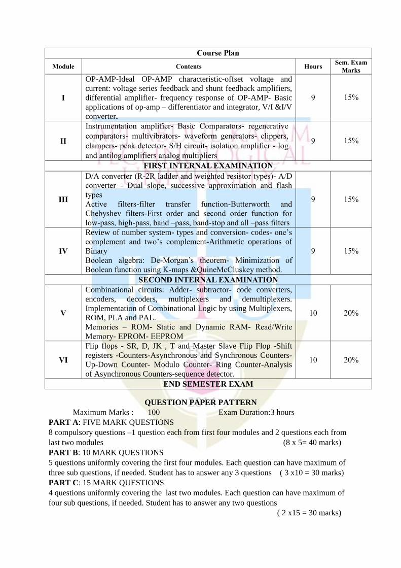
Course Plan
Module Contents Hours Sem. Exam
Marks
I
OP-AMP-Ideal OP-AMP characteristic-offset voltage and
current: voltage series feedback and shunt feedback amplifiers,
differential amplifier- frequency response of OP-AMP- Basic
applications of op-amp – differentiator and integrator, V/I &I/V
converter.
9 15%
II
Instrumentation amplifier- Basic Comparators- regenerative
comparators- multivibrators- waveform generators- clippers,
clampers- peak detector- S/H circuit- isolation amplifier - log
and antilog amplifiers analog multipliers
9 15%
FIRST INTERNAL EXAMINATION
III
D/A converter (R-2R ladder and weighted resistor types)- A/D
converter - Dual slope, successive approximation and flash
types
Active filters-filter transfer function-Butterworth and
Chebyshev filters-First order and second order function for
low-pass, high-pass, band –pass, band-stop and all –pass filters
9 15%
IV
Review of number system- types and conversion- codes- one’s
complement and two’s complement-Arithmetic operations of
Binary
Boolean algebra: De-Morgan’s theorem- Minimization of
Boolean function using K-maps &QuineMcCluskey method.
9 15%
SECOND INTERNAL EXAMINATION
V
Combinational circuits: Adder- subtractor- code converters,
encoders, decoders, multiplexers and demultiplexers.
Implementation of Combinational Logic by using Multiplexers,
ROM, PLA and PAL.
Memories – ROM- Static and Dynamic RAM- Read/Write
Memory- EPROM- EEPROM
10 20%
VI
Flip flops - SR, D, JK , T and Master Slave Flip Flop -Shift
registers -Counters-Asynchronous and Synchronous Counters-
Up-Down Counter- Modulo Counter- Ring Counter-Analysis
of Asynchronous Counters-sequence detector.
10 20%
END SEMESTER EXAM
QUESTION PAPER PATTERN
Maximum Marks : 100 Exam Duration:3 hours
PART A: FIVE MARK QUESTIONS
8 compulsory questions –1 question each from first four modules and 2 questions each from
last two modules (8 x 5= 40 marks)
PART B: 10 MARK QUESTIONS
5 questions uniformly covering the first four modules. Each question can have maximum of
three sub questions, if needed. Student has to answer any 3 questions ( 3 x10 = 30 marks)
PART C: 15 MARK QUESTIONS
4 questions uniformly covering the last two modules. Each question can have maximum of
four sub questions, if needed. Student has to answer any two questions
( 2 x15 = 30 marks)
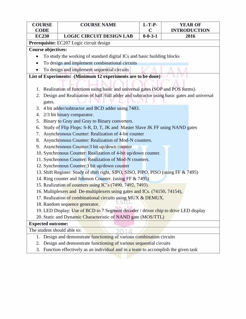
COURSE
CODE
COURSE NAME L-T-P-
C
YEAR OF
INTRODUCTION
EC230 LOGIC CIRCUIT DESIGN LAB 0-0-3-1 2016
Prerequisite: EC207 Logic circuit design
Course objectives:
To study the working of standard digital ICs and basic building blocks
To design and implement combinational circuits
To design and implement sequential circuits
List of Experiments: (Minimum 12 experiments are to be done)
1. Realization of functions using basic and universal gates (SOP and POS forms).
2. Design and Realization of half /full adder and subtractor using basic gates and universal
gates.
3. 4 bit adder/subtractor and BCD adder using 7483.
4. 2/3 bit binary comparator.
5. Binary to Gray and Gray to Binary converters.
6. Study of Flip Flops: S-R, D, T, JK and Master Slave JK FF using NAND gates
7. Asynchronous Counter: Realization of 4-bit counter
8. Asynchronous Counter: Realization of Mod-N counters.
9. Asynchronous Counter:3 bit up/down counter
10. Synchronous Counter: Realization of 4-bit up/down counter.
11. Synchronous Counter: Realization of Mod-N counters.
12. Synchronous Counter:3 bit up/down counter
13. Shift Register: Study of shift right, SIPO, SISO, PIPO, PISO (using FF & 7495)
14. Ring counter and Johnson Counter. (using FF & 7495)
15. Realization of counters using IC’s (7490, 7492, 7493).
16. Multiplexers and De-multiplexers using gates and ICs. (74150, 74154),
17. Realization of combinational circuits using MUX & DEMUX.
18. Random sequence generator.
19. LED Display: Use of BCD to 7 Segment decoder / driver chip to drive LED display
20. Static and Dynamic Characteristic of NAND gate (MOS/TTL)
Expected outcome:
The student should able to:
1. Design and demonstrate functioning of various combination circuits
2. Design and demonstrate functioning of various sequential circuits
3. Function effectively as an individual and in a team to accomplish the given task
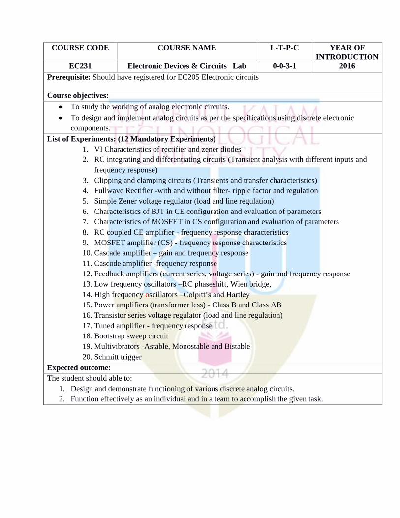
COURSE CODE COURSE NAME L-T-P-C YEAR OF
INTRODUCTION
EC231 Electronic Devices & Circuits Lab 0-0-3-1 2016
Prerequisite: Should have registered for EC205 Electronic circuits
Course objectives:
To study the working of analog electronic circuits.
To design and implement analog circuits as per the specifications using discrete electronic
components.
List of Experiments: (12 Mandatory Experiments)
1. VI Characteristics of rectifier and zener diodes
2. RC integrating and differentiating circuits (Transient analysis with different inputs and
frequency response)
3. Clipping and clamping circuits (Transients and transfer characteristics)
4. Fullwave Rectifier -with and without filter- ripple factor and regulation
5. Simple Zener voltage regulator (load and line regulation)
6. Characteristics of BJT in CE configuration and evaluation of parameters
7. Characteristics of MOSFET in CS configuration and evaluation of parameters
8. RC coupled CE amplifier - frequency response characteristics
9. MOSFET amplifier (CS) - frequency response characteristics
10. Cascade amplifier – gain and frequency response
11. Cascode amplifier -frequency response
12. Feedback amplifiers (current series, voltage series) - gain and frequency response
13. Low frequency oscillators –RC phaseshift, Wien bridge,
14. High frequency oscillators –Colpitt’s and Hartley
15. Power amplifiers (transformer less) - Class B and Class AB
16. Transistor series voltage regulator (load and line regulation)
17. Tuned amplifier - frequency response
18. Bootstrap sweep circuit
19. Multivibrators -Astable, Monostable and Bistable
20. Schmitt trigger
Expected outcome:
The student should able to:
1. Design and demonstrate functioning of various discrete analog circuits.
2. Function effectively as an individual and in a team to accomplish the given task.
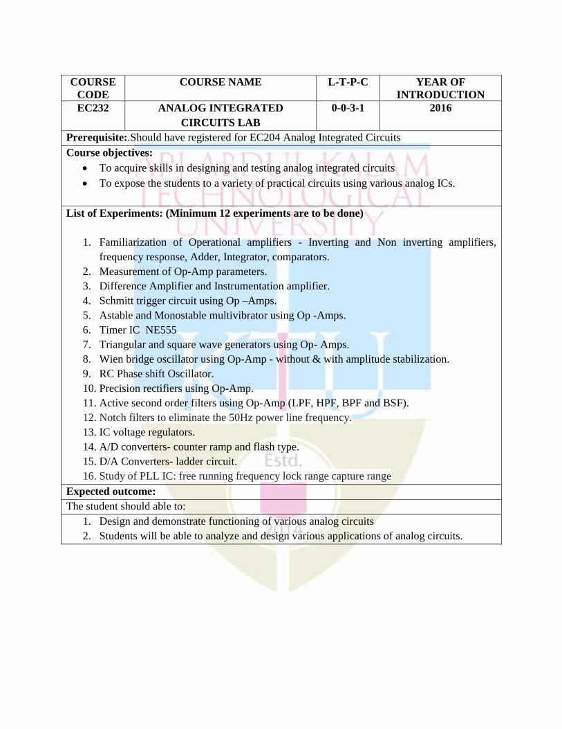
COURSE
CODE
COURSE NAME L-T-P-C YEAR OF
INTRODUCTION
EC232 ANALOG INTEGRATED
CIRCUITS LAB
0-0-3-1 2016
Prerequisite:.Should have registered for EC204 Analog Integrated Circuits
Course objectives:
To acquire skills in designing and testing analog integrated circuits
To expose the students to a variety of practical circuits using various analog ICs.
List of Experiments: (Minimum 12 experiments are to be done)
1. Familiarization of Operational amplifiers - Inverting and Non inverting amplifiers,
frequency response, Adder, Integrator, comparators.
2. Measurement of Op-Amp parameters.
3. Difference Amplifier and Instrumentation amplifier.
4. Schmitt trigger circuit using Op –Amps.
5. Astable and Monostable multivibrator using Op -Amps.
6. Timer IC NE555
7. Triangular and square wave generators using Op- Amps.
8. Wien bridge oscillator using Op-Amp - without & with amplitude stabilization.
9. RC Phase shift Oscillator.
10. Precision rectifiers using Op-Amp.
11. Active second order filters using Op-Amp (LPF, HPF, BPF and BSF).
12. Notch filters to eliminate the 50Hz power line frequency.
13. IC voltage regulators.
14. A/D converters- counter ramp and flash type.
15. D/A Converters- ladder circuit.
16. Study of PLL IC: free running frequency lock range capture range
Expected outcome:
The student should able to:
1. Design and demonstrate functioning of various analog circuits
2. Students will be able to analyze and design various applications of analog circuits.
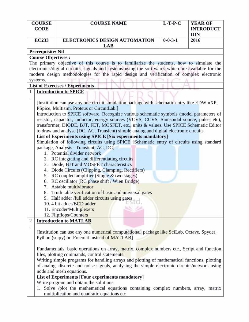
COURSE
CODE
COURSE NAME L-T-P-C YEAR OF
INTRODUCT
ION
EC233 ELECTRONICS DESIGN AUTOMATION
LAB
0-0-3-1 2016
Prerequisite: Nil
Course Objectives :
The primary objective of this course is to familiarize the students, how to simulate the
electronics/digital circuits, signals and systems using the soft-wares which are available for the
modern design methodologies for the rapid design and verification of complex electronic
systems.
List of Exercises / Experiments
1
. Introduction to SPICE
[Institution can use any one circuit simulation package with schematic entry like EDWinXP,
PSpice, Multisim, Proteus or CircuitLab.]
Introduction to SPICE software. Recognize various schematic symbols /model parameters of
resistor, capacitor, inductor, energy sources (VCVS, CCVS, Sinusoidal source, pulse, etc),
transformer, DIODE, BJT, FET, MOSFET, etc., units & values. Use SPICE Schematic Editor
to draw and analyse (DC, AC, Transient) simple analog and digital electronic circuits.
List of Experiments using SPICE [Six experiments mandatory]
Simulation of following circuits using SPICE [Schematic entry of circuits using standard
package, Analysis –Transient, AC, DC]
1. Potential divider network
2. RC integrating and differentiating circuits
3. Diode, BJT and MOSFET characteristics
4. Diode Circuits (Clipping, Clamping, Rectifiers)
5. RC coupled amplifier (Single & two stages)
6. RC oscillator (RC phase shift / Wien Bridge)
7. Astable multivibrator
8. Truth table verification of basic and universal gates
9. Half adder /full adder circuits using gates
10. 4 bit adder/BCD adder
11. Encoder/Multiplexers
12. Flipflops/Counters
2
. Introduction to MATLAB
[Institution can use any one numerical computational package like SciLab, Octave, Spyder,
Python (scipy) or Freemat instead of MATLAB]
Fundamentals, basic operations on array, matrix, complex numbers etc., Script and function
files, plotting commands, control statements.
Writing simple programs for handling arrays and plotting of mathematical functions, plotting
of analog, discrete and noise signals, analysing the simple electronic circuits/network using
node and mesh equations.
List of Experiments [Four experiments mandatory]
Write program and obtain the solutions
1. Solve /plot the mathematical equations containing complex numbers, array, matrix
multiplication and quadratic equations etc
2. Obtain different types of plots (2D/3D, surface plot, polar plot)
3. Generate and plot various signals like sine square, pulse in same window.
4. Plot the diode/transistor characteristics.
5. Solve node, mesh and loop equations of simple electrical/network circuits.
6. Find the poles and zeros hence plot the transfer functions/polynomials
7. Sort numbers in ascending order and save to another text file using text read and sort
function after reading n floating point numbers from a formatted text file stored in the
system.
8. Plot a full wave rectified waveform using Fourier series
3 Introduction to HDL
[Institution can choose VHDL or Verilog as language to describe the problem and any one
simulation/synthesis tool like Xilinix ISE, Modelsim, QSim, verilog, VHDL, EDwinXP or
ORCAD etc. for the simulation.]
List of Experiments using HDL
Write the HDL code to realise and simulate the following circuits: (at least 4 of the following)
1. Basic gates/universal gates
2. Combinational Circuits (Half adder/Half subtractor)
3. Full adder in 3 modelling styles (Dataflow/structural/Behavioural)
4. Multiplexer/De-multiplexer
5. Decoder/Encoder
6. 4 bit adder/BCD adder
7. Flipflops (SR,JK,T,D)
8. Binary Counters
9. Finite state machines
Expected outcomes:
1. An ability to apply knowledge of computer, science, and engineering to the analysis of
electrical and electronic engineering problems.
2. An ability to design systems which include hardware and software components.
3. An ability to identify, formulate and solve engineering problems.
4. An ability to use modern engineering techniques
Course code Course Name L-T-P - Credits Year of
Introduction
EC234 Linear Integrated Circuits and
Digital Electronics Laboratory
0-0-3--1 2016
Prerequisite: EC212 Linear integrated circuits and digital electronics
Course Objectives
To study various digital and linear integrated circuits used in simple system configuration
List of Exercises/Experiments : (10 experiments are mandatory)
1. Operational Amplifiers (IC741)-Characteristics
2. Square , triangular and ramp generation using op-amps
3. Log and Antilog amplifiers.
5. Astable and monostable multivibrators using op-amps
6. Active notch filter realization using op-amps
7. Wein bridges oscillator using OpAmp
8.OpAmp Integrator and Differentiator.
9.Code converter - Binary to gray and Gray to binary.
10.Adder and Subtractor Circuits using logic IC
11.Implementation of combinational logic circuits using MUX IC
12.Design and implementation of multiplexer and demultiplexer.
13.3-bit synchronous counter design
14.Asynchronous counter design and Mod-n counter
15.Shift registers - SISO/SIPO & PISO/PIPO
16.Ring and Johnson Counters
List of major equipment
CRO, Function generator , Single power supply , Dual power supply, Digital multimeter,
Ammeter ,Voltmeter.
Expected outcome . On completion ,the students will be able to
1. Design simple circuits like amplifiers using OP-AMPs.
2. Design waveform Generating circuits.
3. Understand Digital concepts
4. Logically explain the concepts of combinational and sequential circuits.
Text Book:
1.RamakantA.Gayakward, Op-amps and Linear Integrated Circuits, IV edition, Pearson
Education, 2003 / PHI.
2. D.RoyChoudhary, SheilB.Jani, Linear Integrated Circuits, II edition, New Age, 2003.
3. M. Morris Mano, Digital Logic and Computer Design, Prentice Hall of India, 2002
Course code Course Name L-T-P - Credits Year of
Introduction
EC235 ANALOG ELECTRONICS
LABORATORY
0-0-3:1 2016
Prerequisite: EC209 Analog electronics
Course Objectives
To develop working knowledge on electronic devices and their performance characteristics
List of Exercises/Experiments : (Ten experiments are mandatory)
1. Study & Use of CRO: Measurement of current voltage, frequency and phase shift.
2.Diode Clipping Circuits
3. Clamping Circuits
4. Rectifiers and filters with and without shunt capacitors- Characteristics full wave rectifier-
Ripple factor, Rectification efficiency, and % regulation
5. RC coupled amplifier using BJT in CE configuration- Measurement of gain, input and output
impedance and frequency response
6. FET amplifier- Measurement of voltage gain, current gain, input and output impedance
7. Darlington Emitter Follower
8. R.C. Phase Shift Oscillator using BJT or Op- Amp
9. Characteristics of voltage regulators- Design and testing of: a) simple zener voltage
regulator b) zener regulator with emitter follower output
10. Series & Parallel Resonance Circuits
11. Voltage Series Feedback Amplifier
12. Class ‘B’ Push-Pull Amplifier
13. Astable and monostable multivibrators using IC 555
14. Design of PLL for given lock and capture ranges& frequency multiplication
15. Applications using PLL
List of major equipments
CRO, Function generator, Regulated power supply , Dual power supply, Digital multimeter,
Ammeter ,Voltmeter.
Expected outcome.
On completion of the course the student will be able to understand the working of
electrical devices ,their performance characteristics and will be able to design circuits for
various electronic devices
Text Book:
Allen Mottershead, Electronic Devices and Circuits: An Introduction, Prentice Hall of India
![fileCourse syllabus must be attached and completed according to Fitchburg State guidelines. E] Course Syllabus attached Required Signatures—Graduate and Continuing Education Course](https://img.pdfslide.us/doc/110x75/5e122588a8321604d45edfb8/syllabus-must-be-attached-and-completed-according-to-fitchburg-state-guidelines.jpg)