Embed Size (px)
Citation preview
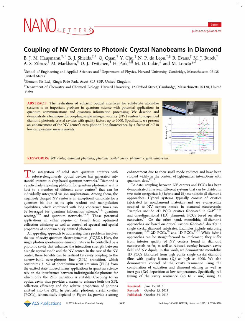
Coupling of NV Centers to Photonic Crystal Nanobeams in DiamondB. J. M. Hausmann,†,⊥ B. J. Shields,‡,⊥ Q. Quan,† Y. Chu,‡ N. P. de Leon,‡,∥ R. Evans,‡ M. J. Burek,†
A. S. Zibrov,‡ M. Markham,§ D. J. Twitchen,§ H. Park,‡,∥ M. D. Lukin,‡ and M. Loncar*,†
†School of Engineering and Applied Sciences and ‡Department of Physics, Harvard University, Cambridge, Massachusetts 02138,United States§Element Six Ltd., King’s Ride Park, Ascot SL5 8BP, United Kingdom∥Department of Chemistry and Chemical Biology, Harvard University, 12 Oxford Street, Cambridge, Massachusetts 02138, UnitedStates
ABSTRACT: The realization of efficient optical interfaces for solid-state atom-likesystems is an important problem in quantum science with potential applications inquantum communications and quantum information processing. We describe anddemonstrate a technique for coupling single nitrogen vacancy (NV) centers to suspendeddiamond photonic crystal cavities with quality factors up to 6000. Specifically, we presentan enhancement of the NV center’s zero-phonon line fluorescence by a factor of ∼7 inlow-temperature measurements.
KEYWORDS: NV center, diamond photonics, photonic crystal cavity, photonic crystal nanobeam
The integration of solid state quantum emitters withsubwavelength-scale optical devices has generated sub-
stantial interest in chip-based quantum networks.1 Diamond isa particularly appealing platform for quantum photonics, as it ishost to a number of different color centers2 that can beindividually integrated via ion implantation. Among them, thenegatively charged NV center is an exceptional candidate for aquantum bit due to its spin readout and manipulationcapabilities, which combined with long coherence times canbe leveraged for quantum information science,3−6 quantumsensing,7−9 and quantum networks.10,11 These potentialapplications all either require or benefit from optimizedcollection efficiency as well as control of spectral and spatialproperties of spontaneously emitted photons.An appealing approach to addressing these problems involves
the use of cavity quantum electrodynamics (CQED). Here, thesingle photon spontaneous emission rate can be controlled by aphotonic cavity that enhances the interaction strength betweena single optical mode and the NV center. In the case of the NVcenter, these benefits can be realized by cavity coupling to thenarrow-band zero-phonon line (ZPL) transition, whichconstitutes 3−5% of photoluminescent emission (PLE) fromthe excited state. Indeed, many applications in quantum sciencerely on the interference between indistinguishable photons forwhich only the ZPL transition is suitable. Coupling to anoptical cavity thus provides a means to enhance both the ZPLcollection efficiency and the relative proportion of photonsemitted into the ZPL. In particular, photonic crystal cavities(PCCs), schematically depicted in Figure 1a, provide a strong
enhancement due to their small mode volumes and have beenstudied widely in the context of light-matter interactions withquantum dots.12,13
To date, coupling between NV centers and PCCs has beendemonstrated in several different systems that can be divided intwo main categories: (i) hybrid and (ii) monolithic all-diamondapproaches. Hybrid systems typically consist of cavitiesfabricated in nondiamond materials and are evanescentlycoupled to NV centers hosted in diamond nanocrystals.Examples include 2D PCCs cavities fabricated in GaP14−16
and one-dimensional (1D) plasmonic PCCs based on silvernanowires.17 On the other hand, monolithic, all-diamondapproaches are based on optical cavities fabricated directly insingle crystal diamond substrates. Examples include microringresonators,18,19 2D PCCs,20 and 1D PCCs.21,22 While hybridapproaches can be straightforward to implement, they sufferfrom inferior quality of NV centers found in diamondnanocrystals so far, as well as reduced overlap between cavityfield and NV dipole. In this work, we demonstrate monolithic1D PCCs fabricated from high purity single crystal diamondfilms with quality factors (Q) as high as 6000. We alsodemonstrate control of the cavity resonance using thecombination of oxidation and diamond etching as well asinert-gas (Xe) deposition at low temperatures. Specifically, redtuning of the cavity resonance (up to 7 nm) using Xe
Received: June 15, 2013Revised: October 15, 2013Published: October 24, 2013
Letter
pubs.acs.org/NanoLett
© 2013 American Chemical Society 5791 dx.doi.org/10.1021/nl402174g | Nano Lett. 2013, 13, 5791−5796
deposition, and blue tuning of up to 23 nm was achieved bypostfabrication diamond etching. Using these techniques wewere able to bring the NV center in resonance with the cavitymodes and demonstrate enhancement of the ZPL emission by afactor of 7 at low temperature.To fabricate photonic crystals from a bulk piece of diamond,
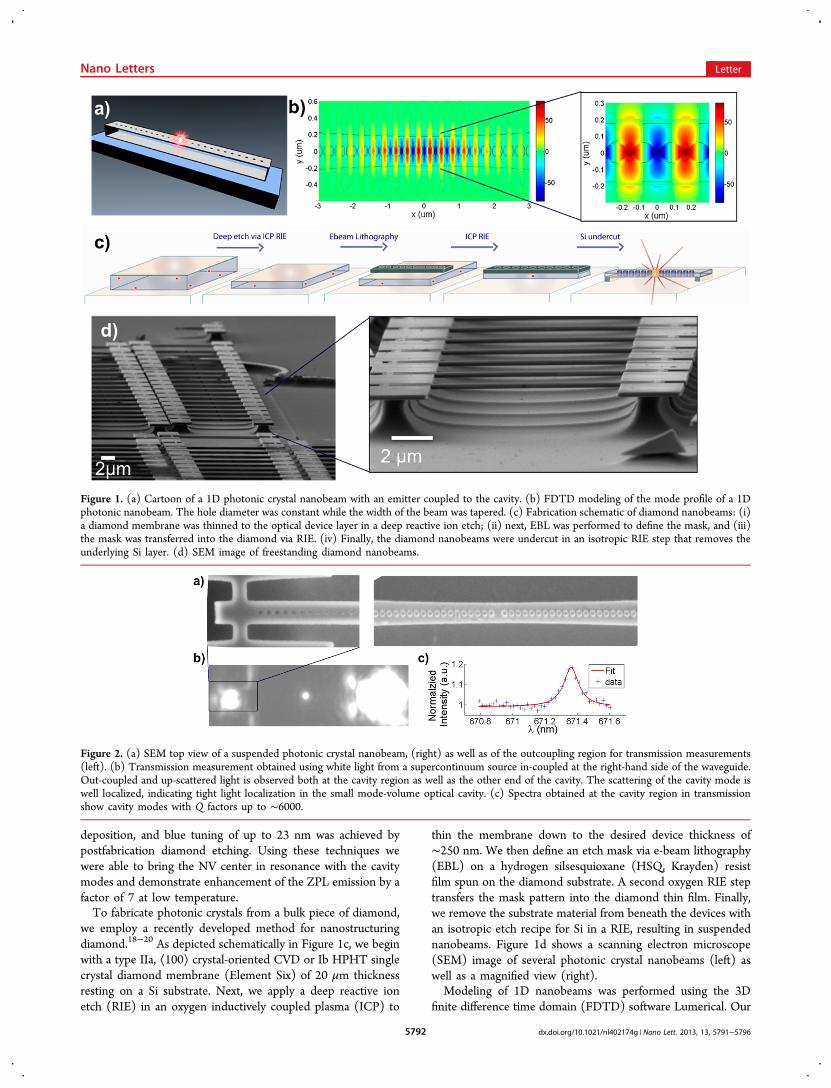
we employ a recently developed method for nanostructuringdiamond.18−20 As depicted schematically in Figure 1c, we beginwith a type IIa, ⟨100⟩ crystal-oriented CVD or Ib HPHT singlecrystal diamond membrane (Element Six) of 20 μm thicknessresting on a Si substrate. Next, we apply a deep reactive ionetch (RIE) in an oxygen inductively coupled plasma (ICP) to
thin the membrane down to the desired device thickness of∼250 nm. We then define an etch mask via e-beam lithography(EBL) on a hydrogen silsesquioxane (HSQ, Krayden) resistfilm spun on the diamond substrate. A second oxygen RIE steptransfers the mask pattern into the diamond thin film. Finally,we remove the substrate material from beneath the devices withan isotropic etch recipe for Si in a RIE, resulting in suspendednanobeams. Figure 1d shows a scanning electron microscope(SEM) image of several photonic crystal nanobeams (left) aswell as a magnified view (right).Modeling of 1D nanobeams was performed using the 3D
finite difference time domain (FDTD) software Lumerical. Our
Figure 1. (a) Cartoon of a 1D photonic crystal nanobeam with an emitter coupled to the cavity. (b) FDTD modeling of the mode profile of a 1Dphotonic nanobeam. The hole diameter was constant while the width of the beam was tapered. (c) Fabrication schematic of diamond nanobeams: (i)a diamond membrane was thinned to the optical device layer in a deep reactive ion etch; (ii) next, EBL was performed to define the mask, and (iii)the mask was transferred into the diamond via RIE. (iv) Finally, the diamond nanobeams were undercut in an isotropic RIE step that removes theunderlying Si layer. (d) SEM image of freestanding diamond nanobeams.
Figure 2. (a) SEM top view of a suspended photonic crystal nanobeam, (right) as well as of the outcoupling region for transmission measurements(left). (b) Transmission measurement obtained using white light from a supercontinuum source in-coupled at the right-hand side of the waveguide.Out-coupled and up-scattered light is observed both at the cavity region as well as the other end of the cavity. The scattering of the cavity mode iswell localized, indicating tight light localization in the small mode-volume optical cavity. (c) Spectra obtained at the cavity region in transmissionshow cavity modes with Q factors up to ∼6000.
Nano Letters Letter
dx.doi.org/10.1021/nl402174g | Nano Lett. 2013, 13, 5791−57965792
photonic crystals consist of a series of holes etched through adiamond ridge waveguide, illustrated schematically in Figure 1a.Light is confined to the waveguide by the index contrastbetween diamond (n = 2.4) and air, while the periodicity of theholes forms a bandgap to confine light along the waveguide.The ability to store light in the cavity region in the time domaincan be quantified by the Q factor. The particular parameters ofour design were chosen to accommodate the inaccuracies ofour fabrication process. In particular, devices obtained from theabove procedure exhibit significant thickness variations fromdevice to device across a single chip, owing to an initialthickness gradient in the mechanically polished diamondmembrane, which is transferred to the film in the deep RIEstep. As a result, we designed our photonic crystals to be robustto moderate variations in thickness within the range of 200−400 nm. To accomplish this, we used a relatively large holeradius (65 nm) and periodicity (ranging from 165 nm to 175nm), which were kept uniform across the entire photoniccrystal. The cavity is then formed by tapering the width of thewaveguide down from 500 nm at the ends to 400 nm at thecavity center in a parabolic profile.23,24 Coupling between thenanobeam photonic crystal cavity and an optical waveguide canbe easily achieved25 by modifying the geometry of the mirrorholes at the ends of the photonic crystal. This allows forintegration of multiple devices on the same chip and realizationof integrated quantum networks. To achieve a high trans-mission signal (T ∝ Qt
2/Qwg2 ), the scattering Q factor (Q ≈ 8 ×
106) was designed much larger than the waveguide Q. Thewaveguide limited (Q ≈ 5.3 × 10⁵), total Q factor wasdetermined to reach values up to Q ≈ 5 × 10⁵ with a modevolume of 1.8 × (λ/n)3, concentrated in the diamond (Figure1b). Photons coupled into the optical waveguides were
outcoupled at the end facet of the waveguide and collectedusing a lens with large numerical aperture (Figure 2a (left)).In addition, we explore an alternative cavity design with a
central hole removed. This cavity geometry features amoderate, scattering limited Q factor (Qscattering = 1 × 10⁴ <Qwaveguide), mode volume of 3.7 (λ/n)
3 and multimode behaviorbut in turn increases the likelihood of locating an NV center inthe cavity center. A top-view of a suspended nanobeamshowing the width taper and filled in hole is presented in Figure2a (right).Characterization of the cavity spectral properties is
performed in two ways. First, we probe the cavity responseto a broadband input in a transmission configuration. We excitewaveguide modes of the diamond nanobeam by coupling whitelight from a supercontinuum source (NKT Photonics) into thewaveguide at one end. Light that is resonant will then couple tothe cavity mode and, depending on the cavity design, either bescattered out from the cavity or transmitted to the far end ofthe waveguide and then outcoupled at the waveguide end. Thebalance between these two processes is determined by the ratioof scattering to waveguide-coupling Q factor. Figure 2billustrates this behavior, with light focused onto the right endof the device and scattered from a well-localized spot at thecavity center and from the outcoupler at the left end of thewaveguide. We collect the scattered light from each locationand analyze its spectrum to obtain the cavity resonancefrequency and Q factor (Figure 2c). With this method, wemeasured spectrometer-limited Q factors exceeding 6,000.For devices containing an NV center, the cavity spectral
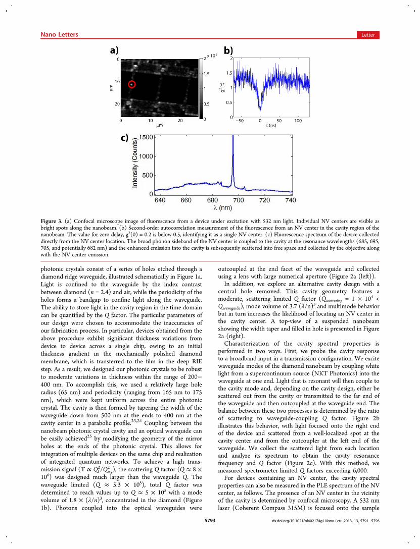
properties can also be measured in the PLE spectrum of the NVcenter, as follows. The presence of an NV center in the vicinityof the cavity is determined by confocal microscopy. A 532 nmlaser (Coherent Compass 315M) is focused onto the sample
Figure 3. (a) Confocal microscope image of fluorescence from a device under excitation with 532 nm light. Individual NV centers are visible asbright spots along the nanobeam. (b) Second-order autocorrelation measurement of the fluorescence from an NV center in the cavity region of thenanobeam. The value for zero delay, g2(0) = 0.2 is below 0.5, identifying it as a single NV center. (c) Fluorescence spectrum of the device collecteddirectly from the NV center location. The broad phonon sideband of the NV center is coupled to the cavity at the resonance wavelengths (685, 695,705, and potentially 682 nm) and the enhanced emission into the cavity is subsequently scattered into free space and collected by the objective alongwith the NV center emission.
Nano Letters Letter
dx.doi.org/10.1021/nl402174g | Nano Lett. 2013, 13, 5791−57965793
and scanned over the field of view to excite randomlypositioned NV centers defined during the growth of thediamond. Photons emitted from an NV center are thencollected (green light is filtered out) and NV centers areidentified as bright spots (Figure 3a). The presence of singleNV centers was established by measuring the second-orderautocorrelation of the PLE signal due to their characteristicantibunching dip (Figure 3b).26 The (overall, non-filtered) NVPLE contains components from both charge states (NV− andNV0) and away from the ZPL provides a relatively flat,broadband source with which to probe the frequency of cavitymodes over a range from ∼575 to 800 nm. The emission of theNV center coupled to the cavity thus exhibits intensity peaks atthe cavity resonances on top of a broad fluorescent background(Figure 3c). This approach can also be used to infer both thecavity frequency and Q factor, and these values were found tobe in good agreement with values obtained using the white lighttransmission measurements. To further study our NV-cavitymodel system, we investigated the effects that the cavity has onthe ZPL emission of the NV.Integration of our cavities with NV centers for quantum
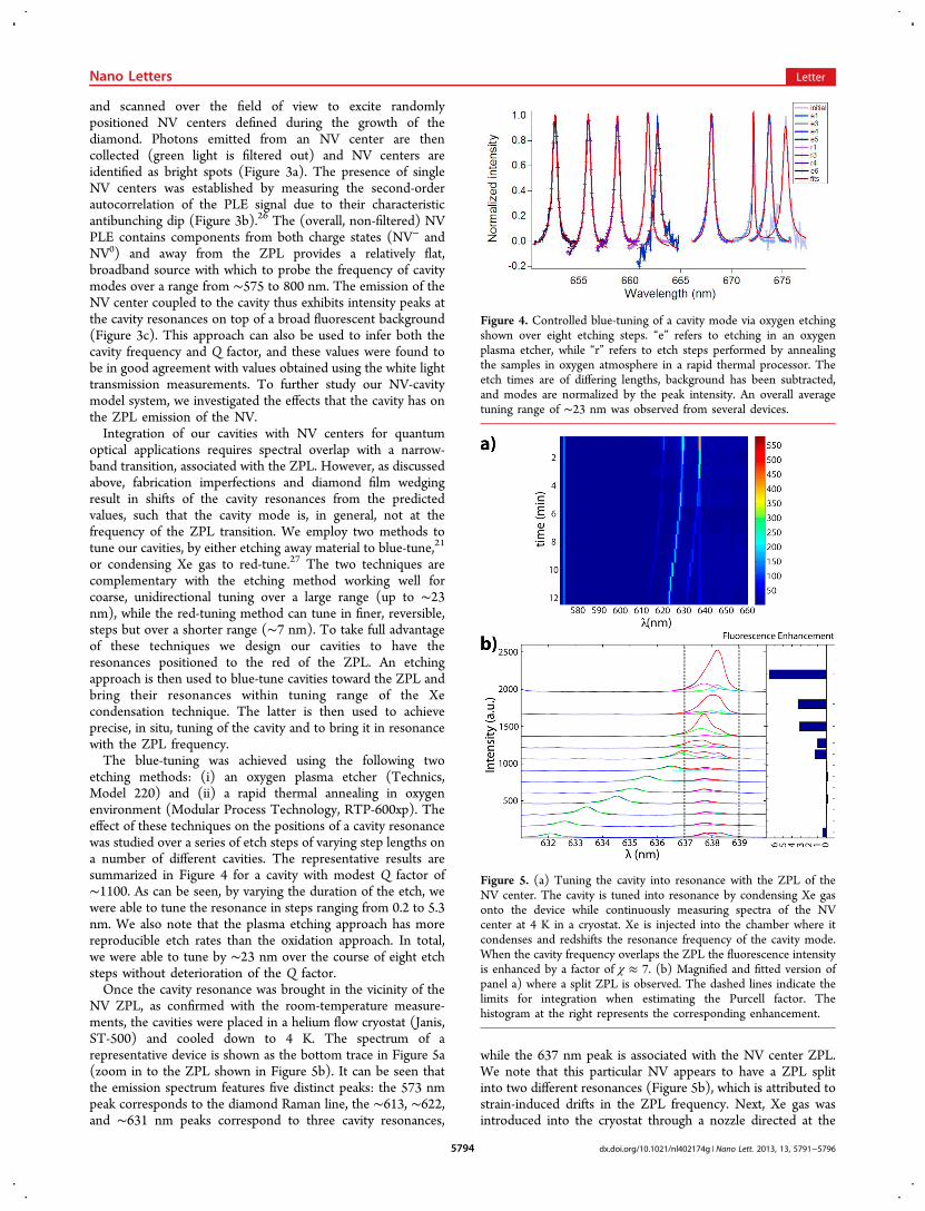
optical applications requires spectral overlap with a narrow-band transition, associated with the ZPL. However, as discussedabove, fabrication imperfections and diamond film wedgingresult in shifts of the cavity resonances from the predictedvalues, such that the cavity mode is, in general, not at thefrequency of the ZPL transition. We employ two methods totune our cavities, by either etching away material to blue-tune,21
or condensing Xe gas to red-tune.27 The two techniques arecomplementary with the etching method working well forcoarse, unidirectional tuning over a large range (up to ∼23nm), while the red-tuning method can tune in finer, reversible,steps but over a shorter range (∼7 nm). To take full advantageof these techniques we design our cavities to have theresonances positioned to the red of the ZPL. An etchingapproach is then used to blue-tune cavities toward the ZPL andbring their resonances within tuning range of the Xecondensation technique. The latter is then used to achieveprecise, in situ, tuning of the cavity and to bring it in resonancewith the ZPL frequency.The blue-tuning was achieved using the following two
etching methods: (i) an oxygen plasma etcher (Technics,Model 220) and (ii) a rapid thermal annealing in oxygenenvironment (Modular Process Technology, RTP-600xp). Theeffect of these techniques on the positions of a cavity resonancewas studied over a series of etch steps of varying step lengths ona number of different cavities. The representative results aresummarized in Figure 4 for a cavity with modest Q factor of∼1100. As can be seen, by varying the duration of the etch, wewere able to tune the resonance in steps ranging from 0.2 to 5.3nm. We also note that the plasma etching approach has morereproducible etch rates than the oxidation approach. In total,we were able to tune by ∼23 nm over the course of eight etchsteps without deterioration of the Q factor.Once the cavity resonance was brought in the vicinity of the
NV ZPL, as confirmed with the room-temperature measure-ments, the cavities were placed in a helium flow cryostat (Janis,ST-500) and cooled down to 4 K. The spectrum of arepresentative device is shown as the bottom trace in Figure 5a(zoom in to the ZPL shown in Figure 5b). It can be seen thatthe emission spectrum features five distinct peaks: the 573 nmpeak corresponds to the diamond Raman line, the ∼613, ∼622,and ∼631 nm peaks correspond to three cavity resonances,
while the 637 nm peak is associated with the NV center ZPL.We note that this particular NV appears to have a ZPL splitinto two different resonances (Figure 5b), which is attributed tostrain-induced drifts in the ZPL frequency. Next, Xe gas wasintroduced into the cryostat through a nozzle directed at the
Figure 4. Controlled blue-tuning of a cavity mode via oxygen etchingshown over eight etching steps. “e” refers to etching in an oxygenplasma etcher, while “r” refers to etch steps performed by annealingthe samples in oxygen atmosphere in a rapid thermal processor. Theetch times are of differing lengths, background has been subtracted,and modes are normalized by the peak intensity. An overall averagetuning range of ∼23 nm was observed from several devices.
Figure 5. (a) Tuning the cavity into resonance with the ZPL of theNV center. The cavity is tuned into resonance by condensing Xe gasonto the device while continuously measuring spectra of the NVcenter at 4 K in a cryostat. Xe is injected into the chamber where itcondenses and redshifts the resonance frequency of the cavity mode.When the cavity frequency overlaps the ZPL the fluorescence intensityis enhanced by a factor of χ ≈ 7. (b) Magnified and fitted version ofpanel a) where a split ZPL is observed. The dashed lines indicate thelimits for integration when estimating the Purcell factor. Thehistogram at the right represents the corresponding enhancement.
Nano Letters Letter
dx.doi.org/10.1021/nl402174g | Nano Lett. 2013, 13, 5791−57965794
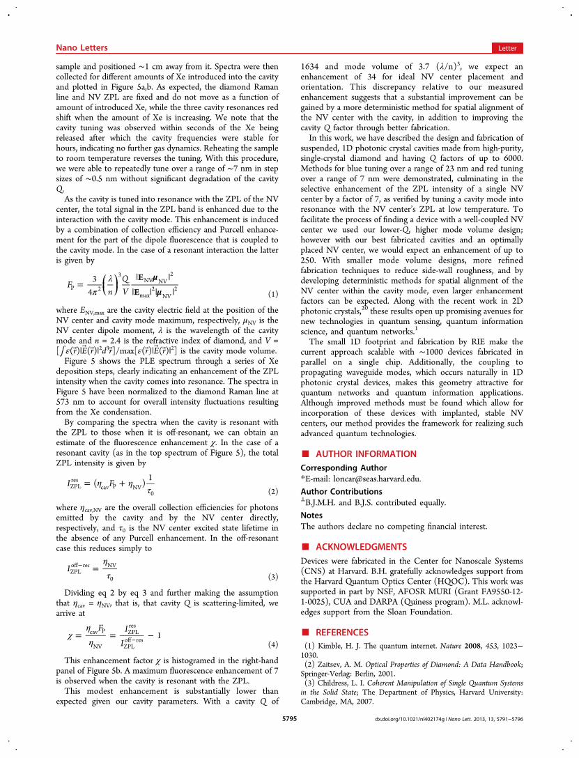
sample and positioned ∼1 cm away from it. Spectra were thencollected for different amounts of Xe introduced into the cavityand plotted in Figure 5a,b. As expected, the diamond Ramanline and NV ZPL are fixed and do not move as a function ofamount of introduced Xe, while the three cavity resonances redshift when the amount of Xe is increasing. We note that thecavity tuning was observed within seconds of the Xe beingreleased after which the cavity frequencies were stable forhours, indicating no further gas dynamics. Reheating the sampleto room temperature reverses the tuning. With this procedure,we were able to repeatedly tune over a range of ∼7 nm in stepsizes of ∼0.5 nm without significant degradation of the cavityQ.As the cavity is tuned into resonance with the ZPL of the NV
center, the total signal in the ZPL band is enhanced due to theinteraction with the cavity mode. This enhancement is inducedby a combination of collection efficiency and Purcell enhance-ment for the part of the dipole fluorescence that is coupled tothe cavity mode. In the case of a resonant interaction the latteris given by
μμπ
λ=| |
| | | |⎜ ⎟⎛⎝
⎞⎠F
nQV
E
E3
4P 2
3NV NV
2
max2
NV2
(1)
where ENV,max are the cavity electric field at the position of theNV center and cavity mode maximum, respectively, μNV is theNV center dipole moment, λ is the wavelength of the cavitymode and n = 2.4 is the refractive index of diamond, and V =[∫ ε(r)|E(r)|2d3r]/max[ε(r)|E(r)|2] is the cavity mode volume.Figure 5 shows the PLE spectrum through a series of Xe
deposition steps, clearly indicating an enhancement of the ZPLintensity when the cavity comes into resonance. The spectra inFigure 5 have been normalized to the diamond Raman line at573 nm to account for overall intensity fluctuations resultingfrom the Xe condensation.By comparing the spectra when the cavity is resonant with
the ZPL to those when it is off-resonant, we can obtain anestimate of the fluorescence enhancement χ. In the case of aresonant cavity (as in the top spectrum of Figure 5), the totalZPL intensity is given by
η ητ
= +I F( )1
ZPLres
cav P NV0 (2)
where ηcav,NV are the overall collection efficiencies for photonsemitted by the cavity and by the NV center directly,respectively, and τ0 is the NV center excited state lifetime inthe absence of any Purcell enhancement. In the off-resonantcase this reduces simply to
ητ
=−I sZPLoff re NV
0 (3)
Dividing eq 2 by eq 3 and further making the assumptionthat ηcav = ηNV, that is, that cavity Q is scattering-limited, wearrive at
χηη
= = −−
F II
1cav P
NV
ZPLres
ZPLoff res
(4)
This enhancement factor χ is histogramed in the right-handpanel of Figure 5b. A maximum fluorescence enhancement of 7is observed when the cavity is resonant with the ZPL.This modest enhancement is substantially lower than
expected given our cavity parameters. With a cavity Q of
1634 and mode volume of 3.7 (λ/n)3, we expect anenhancement of 34 for ideal NV center placement andorientation. This discrepancy relative to our measuredenhancement suggests that a substantial improvement can begained by a more deterministic method for spatial alignment ofthe NV center with the cavity, in addition to improving thecavity Q factor through better fabrication.In this work, we have described the design and fabrication of
suspended, 1D photonic crystal cavities made from high-purity,single-crystal diamond and having Q factors of up to 6000.Methods for blue tuning over a range of 23 nm and red tuningover a range of 7 nm were demonstrated, culminating in theselective enhancement of the ZPL intensity of a single NVcenter by a factor of 7, as verified by tuning a cavity mode intoresonance with the NV center’s ZPL at low temperature. Tofacilitate the process of finding a device with a well-coupled NVcenter we used our lower-Q, higher mode volume design;however with our best fabricated cavities and an optimallyplaced NV center, we would expect an enhancement of up to250. With smaller mode volume designs, more refinedfabrication techniques to reduce side-wall roughness, and bydeveloping deterministic methods for spatial alignment of theNV center within the cavity mode, even larger enhancementfactors can be expected. Along with the recent work in 2Dphotonic crystals,20 these results open up promising avenues fornew technologies in quantum sensing, quantum informationscience, and quantum networks.1
The small 1D footprint and fabrication by RIE make thecurrent approach scalable with ∼1000 devices fabricated inparallel on a single chip. Additionally, the coupling topropagating waveguide modes, which occurs naturally in 1Dphotonic crystal devices, makes this geometry attractive forquantum networks and quantum information applications.Although improved methods must be found which allow forincorporation of these devices with implanted, stable NVcenters, our method provides the framework for realizing suchadvanced quantum technologies.
■ AUTHOR INFORMATIONCorresponding Author*E-mail: [email protected].
Author Contributions⊥B.J.M.H. and B.J.S. contributed equally.
NotesThe authors declare no competing financial interest.
■ ACKNOWLEDGMENTSDevices were fabricated in the Center for Nanoscale Systems(CNS) at Harvard. B.H. gratefully acknowledges support fromthe Harvard Quantum Optics Center (HQOC). This work wassupported in part by NSF, AFOSR MURI (Grant FA9550-12-1-0025), CUA and DARPA (Quiness program). M.L. acknowl-edges support from the Sloan Foundation.
■ REFERENCES(1) Kimble, H. J. The quantum internet. Nature 2008, 453, 1023−1030.(2) Zaitsev, A. M. Optical Properties of Diamond: A Data Handbook;Springer-Verlag: Berlin, 2001.(3) Childress, L. I. Coherent Manipulation of Single Quantum Systemsin the Solid State; The Department of Physics, Harvard University:Cambridge, MA, 2007.
Nano Letters Letter
dx.doi.org/10.1021/nl402174g | Nano Lett. 2013, 13, 5791−57965795
(4) Wrachtrup, J.; Jelezko, F. Processing quantum information indiamond. J. Phys.: Condens. Matter 2006, 18, S807−S824.(5) O’Brien, J. L. Optical Quantum Computing. Science 2007, 318,1567.(6) Neumann, P.; et al. Multipartite entanglement among single spinsin diamond. Science 2008, 320, 1326.(7) Maze, J. R.; et al. Nanoscale magnetic sensing with an individualelectronic spin in diamond. Nature 2008, 455, 644−648.(8) Balasubramanian, G.; et al. Nanoscale imaging magnetometrywith diamond spins under ambient conditions. Nature 2008, 455,648−651.(9) Maletinsky, P.; et al. A robust scanning diamond sensor fornanoscale imaging with single nitrogen-vacancy centres. Nat. Nano-technol. 2012, 7, 320.(10) Childress, L.; Taylor, J. M.; Sorensen, A. S.; Lukin, M. D. Fault-tolerant quantum communication based on solid-state photonemitters. Phys. Rev. Lett. 2006, 96, 070504.(11) Beveratos, A.; et al. Single photon quantum cryptography. Phys.Rev. Lett. 2002, 89, 187901.(12) Reithmaier, J. P.; et al. Strong coupling in a single quantumdot−semiconductor microcavity system. Nature 2004, 432, 197.(13) Yoshie, T.; et al. Vacuum Rabi splitting with a single quantumdot in a photonic crystal nanocavity. Nature 2004, 432, 200.(14) Englund, D.; et al. Deterministic Coupling of a Single NitrogenVacancy Center to a Photonic Crystal Cavity. Nano Lett. 2010, 10,3922−3926.(15) Wolters, J.; et al. Enhancement of the zero phonon line emissionfrom a single nitrogen vacancy center in a nanodiamond via couplingto a photonic crystal cavity. Appl. Phys. Lett. 2010, 97, 141108.(16) van der Sar, T.; et al. Deterministic nanoassembly of a coupledquantum emitter−photonic crystal cavity system. Appl. Phys. Lett.2011, 98, 193103.(17) de Leon, N. P.; et al. Tailoring Light-Matter Interaction with aNanoscale Plasmon Resonator. Phys. Rev. Lett. 2012, 108, 226803.(18) Faraon, A.; Barclay, P. E.; Santori, C.; Fu, K.-M. C.; Beausoleil,R. G. Resonant enhancement of the zero-phonon emission from acolour centre in a diamond cavity. Nat. Photonics 2011, 5, 301.(19) Hausmann, B. M.; et al. Integrated Diamond Networks forQuantum Nanophotonics. Nano Lett. 2012, 12, 1578.(20) Faraon, A.; Santori, C.; Huang, Z.; Acosta, V. M.; Beausoleil, R.G. Coupling of Nitrogen-Vacancy Centers to Photonic CrystalCavities in Monocrystalline Diamond. Phys. Rev. Lett. 2012, 109,033604.(21) Riedrich-Moeller, J. et al. One- and two-dimensional photoniccrystal microcavities in single crystal diamond. Nat. Nanotechnol. 7(2012).(22) Burek, M. J.; et al. Free-Standing Mechanical and PhotonicNanostructures in Single-Crystal Diamond. Nano Lett. 2012, 12, 6084.(23) Ahn, B. H.; et al. One-dimensional parabolicbeam photoniccrystal laser. Opt. Exp. 2010, 18, 5654−5660.(24) Quan, Q.; Loncar, M. Deterministic design of wavelength scale,ultra-high Q photonic crystal nanobeam cavities. Opt. Exp. 2011, 19,18529−18542.(25) Quan, Q.; Deotare, P. B.; Loncar, M. Photonic crystalnanobeam cavity strongly coupled to the feeding waveguide. Appl.Phys. Lett. 2010, 96, 203102.(26) Kimble, H. J.; Dagenais, M.; Mandel, L. Photon Antibunching inResonance Fluorescence. Phys. Rev. Lett. 1977, 39, 691.(27) Mosor, S.; et al. Scanning a photonic crystal slab nanocavity bycondensation of xenon. Appl. Phys. Lett. 2005, 87, 141105.
Nano Letters Letter
dx.doi.org/10.1021/nl402174g | Nano Lett. 2013, 13, 5791−57965796