Embed Size (px)
Citation preview
Coupled double-layer Fano resonance photonic crystal filters with lattice-displacementYichen Shuai, Deyin Zhao, Arvinder Singh Chadha, Jung-Hun Seo, Hongjun Yang, Shanhui Fan, Zhenqiang Ma
, and Weidong Zhou Citation: Applied Physics Letters 103, 241106 (2013); doi: 10.1063/1.4846475 View online: http://dx.doi.org/10.1063/1.4846475 View Table of Contents: http://scitation.aip.org/content/aip/journal/apl/103/24?ver=pdfcov Published by the AIP Publishing
This article is copyrighted as indicated in the article. Reuse of AIP content is subject to the terms at: http://scitation.aip.org/termsconditions. Downloaded to IP:
123.254.121.195 On: Tue, 10 Dec 2013 21:14:28
Coupled double-layer Fano resonance photonic crystal filterswith lattice-displacement
Yichen Shuai,1 Deyin Zhao,1 Arvinder Singh Chadha,1 Jung-Hun Seo,2 Hongjun Yang,1,3
Shanhui Fan,4 Zhenqiang Ma,2 and Weidong Zhou1,a)
1Department of Electrical Engineering, University of Texas at Arlington, Arlington, Texas 76019, USA2Department of Electrical and Computer Engineering, University of Wisconsin, Madison,Wisconsin 53706, USA3Semerane, Inc., Arlington, Texas 76010, USA4Department of Electrical Engineering, Stanford University, Stanford, California 94305, USA
(Received 22 October 2013; accepted 26 November 2013; published online 10 December 2013)
We present here ultra-compact high-Q Fano resonance filters with displaced lattices between two
coupled photonic crystal slabs, fabricated with crystalline silicon nanomembrane transfer printing
and aligned e-beam lithography techniques. Theoretically, with the control of lattice displacement
between two coupled photonic crystal slabs layers, optical filter Q factors can approach
211 000 000 for the design considered here. Experimentally, Q factors up to 80 000 have been
demonstrated for a filter design with target Q factor of 130 000. VC 2013 AIP Publishing LLC.
[http://dx.doi.org/10.1063/1.4846475]
In recent years, great interests have been attracted to sin-
gle layer ultra-compact surface-normal nanostructured opti-
cal filters and reflectors1–9 mostly based on one-dimensional
high contrast gratings (1D HCGs)6,10 and two-dimensional
photonic crystal slabs (2D PCSs).4,8,9,11 The phase matching,
provided by in-plane periodic index modulation, enables the
coupling of guided modes with out-of-the-plane radiations,
resulting in Fano interference and guided mode resonance
(GMR) effects.1,2,12,13 Extremely high quality factor (Q)
optical filters can be obtained in these structures with asym-
metric resonance lineshapes due to Fano interference effect,
which creates a sharp transition between transmission peak
and dip.13 Optical filters based on single layer 2D PCSs have
been investigated extensively.3,5,14–20 However, single layer
PCS Fano filters offer limited dispersion engineering capa-
bilities for fine-tuning the output spectrum.
Coupled bi-layer PCS structures, on the other hand,
were proposed and reported to have very high Q factors and
strong optomechanical forces.21,22 Suh et al. and Liu et al.reported previously that optical Q-factors and optomechani-
cal interactions can be controlled by precisely tuning the gap
and the lattice displacement between two coupled PCS.14,23
When considered theoretically, one can achieve infinite Q
factors in the dark states arising from coupled bright or dark
resonances in symmetric or asymmetric coupled bi-layer
PCSs, respectively.23 Using single step e-beam lithography
patterning processes, researchers have experimentally dem-
onstrated coupled bi-layer PCS structures in InP material
systems, with strong optomechanical interactions and modest
Q factors (�1600).24 We also reported that coupled double-
layer Fano resonance PCS filters with experimentally dem-
onstrated Q factor of 9734 and extinction ratio of 8 dB, for a
filter design with a target Q of 22 000.25 In Refs. 24 and 25,
the lattices of holes in the two layers are aligned with respect
to each other. It was established theoretically that allowing
lateral displacement of the lattices in the two layers with
respect to each other would enable an additional degree of
freedom in the control of the filter characteristics of the two-
layer structure.14,23 However, experimental demonstration of
coupled double-layer PCS structures with controlled lattice
displacement has not been reported due to the challenges
associated with its fabrication. Employing PDMS (polydime-
thylsiloxane) nanomembrane transfer printing technique, it is
possible to stack multi-layers of semiconductor and other
dielectric materials.8,26 We report here the design and experi-
mental demonstration of coupled double-layer PCS with pre-
cisely controlled lattice displacement, based on transfer
printing and multi-layer e-beam patterning alignment proc-
esses.26,27 Both simulation and measurement suggest that
optical filter Q factors are very sensitive to the lattice dis-
placement. For one structure with relatively large lattice dis-
placement, we demonstrated a Q factor of 80 000
experimentally. Further design and process optimization lead
us to expect much higher Q-factors with a simulation Q
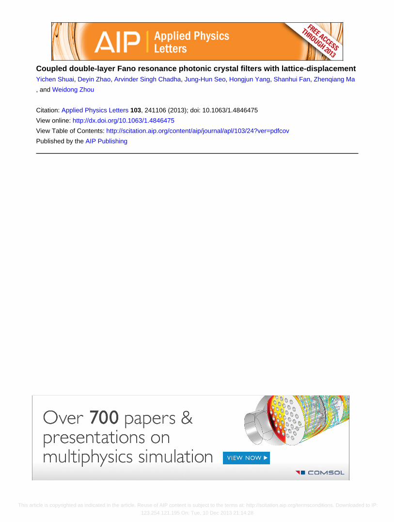
FIG. 1. (a), (b) Schematics of Fano resonance filters based on PDMS trans-
fer printed coupled double layer photonic crystal slab (nanomembrane) on
silicon substrate. (a) 3D close-up view with lattice displacement and thin ox-
ide buffer layer (tb) sandwiched in between two single layer crystalline sili-
con PC layers (t1 and t2); (b) illustration and definition of key design
parameters, including lattice constant (a), air hole radius (r), and lattice dis-
placement (Dx, Dy) between two layers. The inset shows the incident beam
polarization (E-vector) W definition.a)[email protected]
0003-6951/2013/103(24)/241106/5/$30.00 VC 2013 AIP Publishing LLC103, 241106-1
APPLIED PHYSICS LETTERS 103, 241106 (2013)
This article is copyrighted as indicated in the article. Reuse of AIP content is subject to the terms at: http://scitation.aip.org/termsconditions. Downloaded to IP:
123.254.121.195 On: Tue, 10 Dec 2013 21:14:28
factor of 2.11� 108 for coupled double-PCS structures with
optimal lattice displacement.
The optical filter is shown schematically in Fig. 1, where
two single layer PCSs (with thicknesses t1 and t2) are stacked
with controlled lattice displacement (Dx, Dy). An ultra-thin
low index oxide buffer layer (with thicknesses tb) is sand-
wiched in between, serving as the coupling layer. A square
lattice PCS structure was used here with air hole radius (r)
and lattice period (a). The filter transmission and reflection
spectra were computed using the Fourier Modal Method
with a freely available Stanford Stratified Structure Solver
(S4) software package.28 Here we consider surface-normal
incident beams for the filter design and measurement. The
incident beam polarization (E-vector) W is defined as the
angle from the positive x-axis to the polarization direction,
as shown in the inset of Fig. 1(b).
The design parameters are chosen based on the structure
reported earlier,25 with a¼ 1000 nm, r/a¼ 0.08, t1¼ t2¼ 230 nm, tb¼ 20 nm. Simulations were carried out to find
the Q factors for different lattice displacements (Dx, Dy).
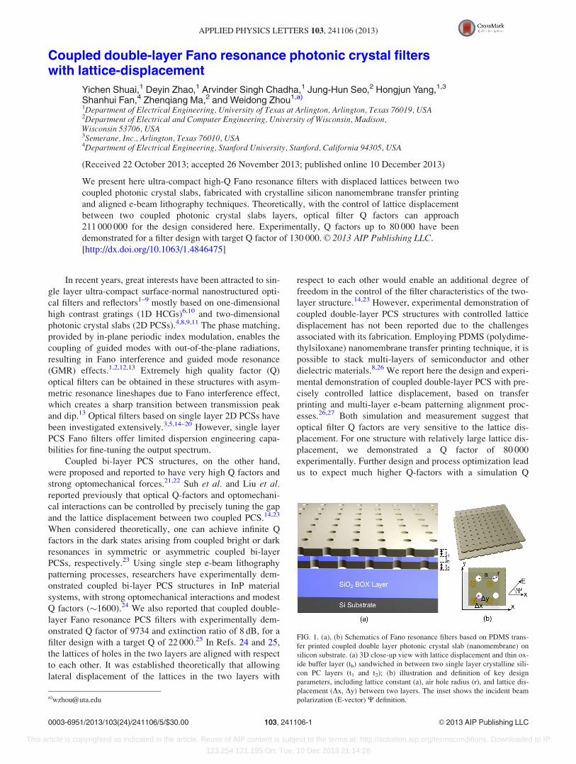
Shown in Fig. 2 are simulated transmission and reflection
spectra for double layer stacked Fano filters without (Figs.
2(a) and 2(c)) and with (Figs. 2(b) and 2(d)) lattice offset
(Dx¼ 0.2a, Dy¼ 0.5a), with the insets showing the zoom-in
plot for the dominant (highest Q) resonance in each case. Also
shown in the insets are the schematics of the structures uti-
lized in the simulation. The transmission spectra shown in
Figs. 2(a) and 2(b) used a glass substrate. The reflection spec-
tra shown in Figs. 2(c) and 2(d) used a SOI substrate. The
results shown in Figs. 2(b) and 2(d) correspond to the highest
Q value obtained for this set of design parameters. Notice that
Fano filter Q increases from 26 000 and 28 000 for the
FIG. 2. Simulated transmission and
reflection spectra for double layer
stacked Fano filters (a), (c) without and
(b), (d) with lattice offset (Dx¼ 0.2a,
Dy¼ 0.5a), with the insets shown the
zoom-in plot for the dominant (high
Qs) resonance for each cases. Also
shown in the insets are the schematics
of the structures considered in the sim-
ulation. For the transmission spectra
shown in (a), (b), glass substrate was
considered. For the reflection spectra
shown in (c), (d), SOI substrate was
considered.
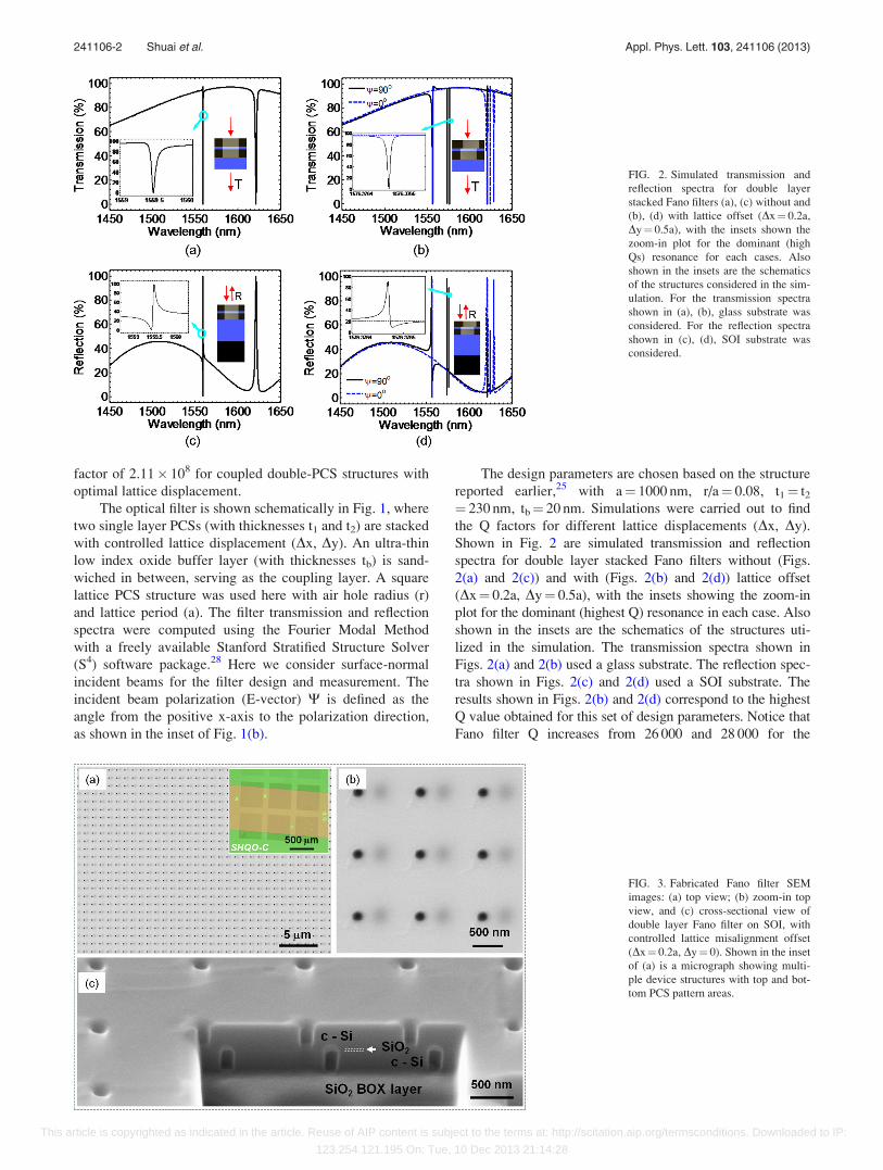
FIG. 3. Fabricated Fano filter SEM
images: (a) top view; (b) zoom-in top
view, and (c) cross-sectional view of
double layer Fano filter on SOI, with
controlled lattice misalignment offset
(Dx¼ 0.2a, Dy¼ 0). Shown in the inset
of (a) is a micrograph showing multi-
ple device structures with top and bot-
tom PCS pattern areas.
241106-2 Shuai et al. Appl. Phys. Lett. 103, 241106 (2013)
This article is copyrighted as indicated in the article. Reuse of AIP content is subject to the terms at: http://scitation.aip.org/termsconditions. Downloaded to IP:
123.254.121.195 On: Tue, 10 Dec 2013 21:14:28
perfectly aligned lattice structures (Figs. 2(a) and 2(c)) to
2.11� 108 and 1.76� 108 for the lattice misaligned structures
(Figs. 2(b) and 2(d)) with an optimal lattice displacement of
Dx¼ 0.2a and Dy¼ 0.5a. It is also worth mentioning that the
low index buffer layer (e.g., SiO2 used here) thickness can
also be varied for Q-factors approaching infinity.23,25
A thin oxide buffer layer (tb¼ 20 nm in this case) was
first formed by thermal oxidation of a single crystalline Si
layer on a SOI substrate, followed by the definition of Cr/Au
global alignment marks based on e-beam lithography (EBL)
and the metal lift-off processes. The bottom PCS structure
was then formed by a 2nd EBL patterning, aligned with the
Cr/Au global alignment marks, and reactive-ion etching
(RIE) dry etching processes. A piece of single crystalline Si
nanomembrane (1 mm� 2 mm size) was released from
another unpatterned SOI substrate and stacked onto the pat-
terned bottom PCS SOI substrate using the PDMS transfer
printing process.8,26 A 3rd EBL step was used to pattern the
top PCS layer, aligned with the same global alignment
marks, with alignment accuracy �10 nm.
With the control of the pattern location, we achieved
precise control of lattice displacement between top and bot-
tom PCS layers. Shown in Fig. 3 are scanning electron
microscope (SEM) images of fabricated double layer PCS
Fano filters with displaced lattices between coupled PCS
layers. The cut-out cross-sectional view SEM image shown
in Fig. 3(c) was prepared with the focused ion beam (FIB)
technique. Clearly, coupled double-layer PCS structures with
oxide buffer were achieved using precisely controlled lattice
displacement (Dx¼ 0.2a, Dy¼ 0). Also shown in the inset of
Fig. 3(a) is a microscopic image of coupled double layer
PCS optical filters with six patterned device structures (bot-
tom squares) and patterned top PCS structures on a piece of
transferred crystalline Si nanomembrane.
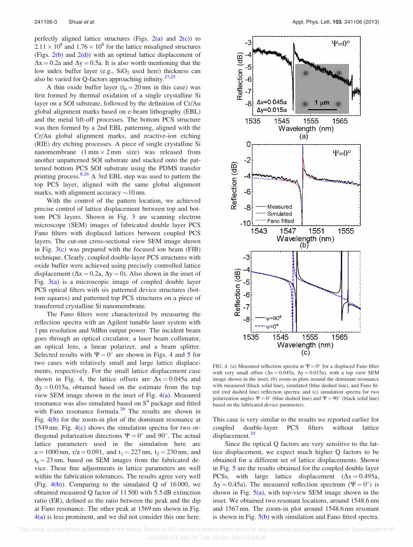
The Fano filters were characterized by measuring the
reflection spectra with an Agilent tunable laser system with
1 pm resolution and 9dBm output power. The incident beam
goes through an optical circulator, a laser beam collimator,
an optical lens, a linear polarizer, and a beam splitter.
Selected results with W¼ 0� are shown in Figs. 4 and 5 for
two cases with relatively small and large lattice displace-
ments, respectively. For the small lattice displacement case
shown in Fig. 4, the lattice offsets are Dx¼ 0.045a and
Dy¼ 0.015a, obtained based on the estimate from the top
view SEM image shown in the inset of Fig. 4(a). Measured
resonance was also simulated based on S4 package and fitted
with Fano resonance formula.29 The results are shown in
Fig. 4(b) for the zoom-in plot of the dominant resonance at
1549 nm. Fig. 4(c) shows the simulation spectra for two or-
thogonal polarization directions W¼ 0� and 90�. The actual
lattice parameters used in the simulation here are
a¼ 1000 nm, r/a¼ 0.091, and t1¼ 227 nm, t2¼ 230 nm, and
tb¼ 23 nm, based on SEM images from the fabricated de-
vice. These fine adjustments in lattice parameters are well
within the fabrication tolerances. The results agree very well
(Fig. 4(b)). Comparing to the simulated Q of 16 000, we
obtained measured Q factor of 11 500 with 5.5 dB extinction
ratio (ER), defined as the ratio between the peak and the dip
at Fano resonance. The other peak at 1569 nm shown in Fig.
4(a) is less prominent, and we did not consider this one here.
This case is very similar to the results we reported earlier for
coupled double-layer PCS filters without lattice
displacement.25
Since the optical Q factors are very sensitive to the lat-
tice displacement, we expect much higher Q factors to be
obtained for a different set of lattice displacements. Shown
in Fig. 5 are the results obtained for the coupled double layer
PCSs, with large lattice displacement (Dx¼ 0.495a,
Dy¼ 0.45a). The measured reflection spectrum (W¼ 0�) is
shown in Fig. 5(a), with top-view SEM image shown in the
inset. We obtained two resonant locations, around 1548.6 nm
and 1567 nm. The zoom-in plot around 1548.6 nm resonant
is shown in Fig. 5(b) with simulation and Fano fitted spectra.
FIG. 4. (a) Measured reflection spectra at W¼ 0� for a displaced Fano filter
with very small offset (Dx¼ 0.045a, Dy¼ 0.015a), with a top view SEM
image shown in the inset; (b) zoom-in plots around the dominant resonance
with measured (black solid line), simulated (blue dashed line), and Fano fit-
ted (red dashed line) reflection spectra; and (c) simulation spectra for two
polarization angles W¼ 0� (blue dashed line) and W¼ 90� (black solid line)
based on the fabricated device parameters.
241106-3 Shuai et al. Appl. Phys. Lett. 103, 241106 (2013)
This article is copyrighted as indicated in the article. Reuse of AIP content is subject to the terms at: http://scitation.aip.org/termsconditions. Downloaded to IP:
123.254.121.195 On: Tue, 10 Dec 2013 21:14:28
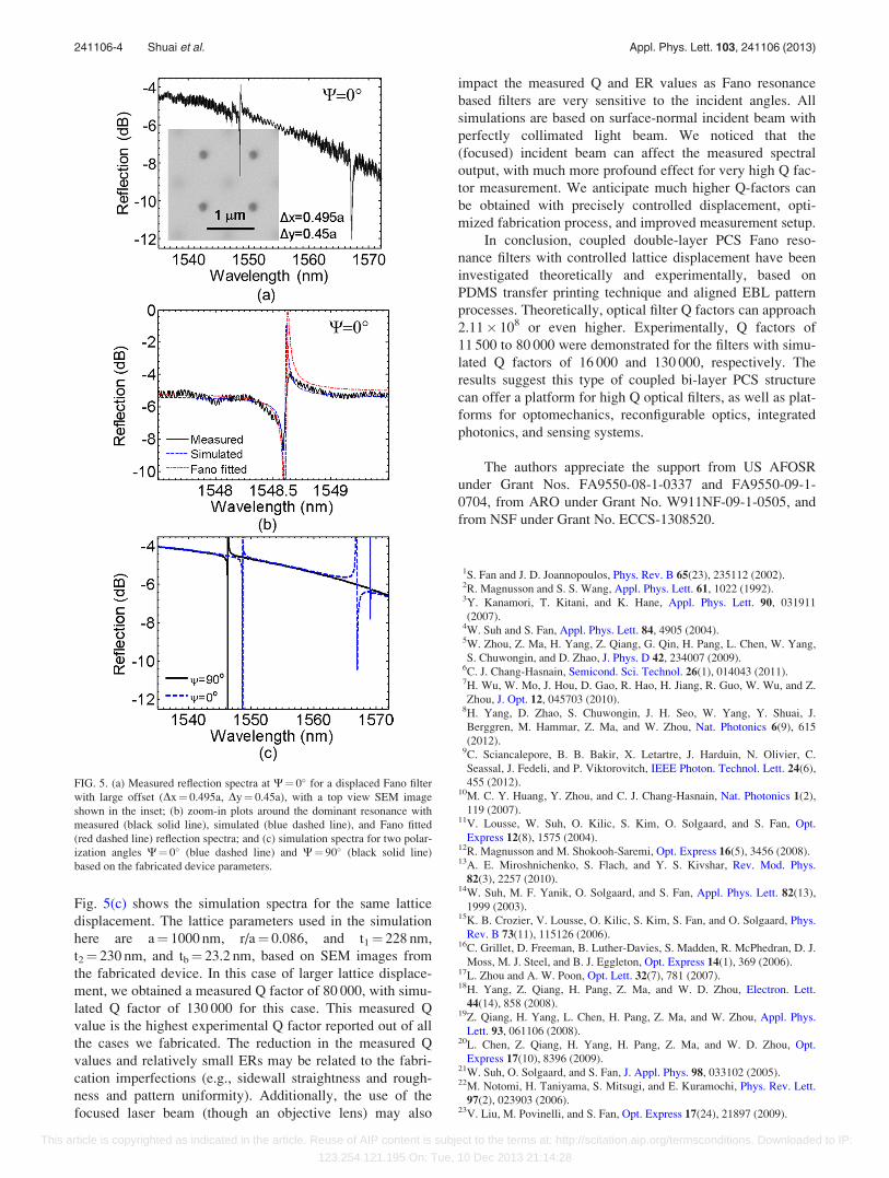
Fig. 5(c) shows the simulation spectra for the same lattice
displacement. The lattice parameters used in the simulation
here are a¼ 1000 nm, r/a¼ 0.086, and t1¼ 228 nm,
t2¼ 230 nm, and tb¼ 23.2 nm, based on SEM images from
the fabricated device. In this case of larger lattice displace-
ment, we obtained a measured Q factor of 80 000, with simu-
lated Q factor of 130 000 for this case. This measured Q
value is the highest experimental Q factor reported out of all
the cases we fabricated. The reduction in the measured Q
values and relatively small ERs may be related to the fabri-
cation imperfections (e.g., sidewall straightness and rough-
ness and pattern uniformity). Additionally, the use of the
focused laser beam (though an objective lens) may also
impact the measured Q and ER values as Fano resonance
based filters are very sensitive to the incident angles. All
simulations are based on surface-normal incident beam with
perfectly collimated light beam. We noticed that the
(focused) incident beam can affect the measured spectral
output, with much more profound effect for very high Q fac-
tor measurement. We anticipate much higher Q-factors can
be obtained with precisely controlled displacement, opti-
mized fabrication process, and improved measurement setup.
In conclusion, coupled double-layer PCS Fano reso-
nance filters with controlled lattice displacement have been
investigated theoretically and experimentally, based on
PDMS transfer printing technique and aligned EBL pattern
processes. Theoretically, optical filter Q factors can approach
2.11� 108 or even higher. Experimentally, Q factors of
11 500 to 80 000 were demonstrated for the filters with simu-
lated Q factors of 16 000 and 130 000, respectively. The
results suggest this type of coupled bi-layer PCS structure
can offer a platform for high Q optical filters, as well as plat-
forms for optomechanics, reconfigurable optics, integrated
photonics, and sensing systems.
The authors appreciate the support from US AFOSR
under Grant Nos. FA9550-08-1-0337 and FA9550-09-1-
0704, from ARO under Grant No. W911NF-09-1-0505, and
from NSF under Grant No. ECCS-1308520.
1S. Fan and J. D. Joannopoulos, Phys. Rev. B 65(23), 235112 (2002).2R. Magnusson and S. S. Wang, Appl. Phys. Lett. 61, 1022 (1992).3Y. Kanamori, T. Kitani, and K. Hane, Appl. Phys. Lett. 90, 031911
(2007).4W. Suh and S. Fan, Appl. Phys. Lett. 84, 4905 (2004).5W. Zhou, Z. Ma, H. Yang, Z. Qiang, G. Qin, H. Pang, L. Chen, W. Yang,
S. Chuwongin, and D. Zhao, J. Phys. D 42, 234007 (2009).6C. J. Chang-Hasnain, Semicond. Sci. Technol. 26(1), 014043 (2011).7H. Wu, W. Mo, J. Hou, D. Gao, R. Hao, H. Jiang, R. Guo, W. Wu, and Z.
Zhou, J. Opt. 12, 045703 (2010).8H. Yang, D. Zhao, S. Chuwongin, J. H. Seo, W. Yang, Y. Shuai, J.
Berggren, M. Hammar, Z. Ma, and W. Zhou, Nat. Photonics 6(9), 615
(2012).9C. Sciancalepore, B. B. Bakir, X. Letartre, J. Harduin, N. Olivier, C.
Seassal, J. Fedeli, and P. Viktorovitch, IEEE Photon. Technol. Lett. 24(6),
455 (2012).10M. C. Y. Huang, Y. Zhou, and C. J. Chang-Hasnain, Nat. Photonics 1(2),
119 (2007).11V. Lousse, W. Suh, O. Kilic, S. Kim, O. Solgaard, and S. Fan, Opt.
Express 12(8), 1575 (2004).12R. Magnusson and M. Shokooh-Saremi, Opt. Express 16(5), 3456 (2008).13A. E. Miroshnichenko, S. Flach, and Y. S. Kivshar, Rev. Mod. Phys.
82(3), 2257 (2010).14W. Suh, M. F. Yanik, O. Solgaard, and S. Fan, Appl. Phys. Lett. 82(13),
1999 (2003).15K. B. Crozier, V. Lousse, O. Kilic, S. Kim, S. Fan, and O. Solgaard, Phys.
Rev. B 73(11), 115126 (2006).16C. Grillet, D. Freeman, B. Luther-Davies, S. Madden, R. McPhedran, D. J.
Moss, M. J. Steel, and B. J. Eggleton, Opt. Express 14(1), 369 (2006).17L. Zhou and A. W. Poon, Opt. Lett. 32(7), 781 (2007).18H. Yang, Z. Qiang, H. Pang, Z. Ma, and W. D. Zhou, Electron. Lett.
44(14), 858 (2008).19Z. Qiang, H. Yang, L. Chen, H. Pang, Z. Ma, and W. Zhou, Appl. Phys.
Lett. 93, 061106 (2008).20L. Chen, Z. Qiang, H. Yang, H. Pang, Z. Ma, and W. D. Zhou, Opt.
Express 17(10), 8396 (2009).21W. Suh, O. Solgaard, and S. Fan, J. Appl. Phys. 98, 033102 (2005).22M. Notomi, H. Taniyama, S. Mitsugi, and E. Kuramochi, Phys. Rev. Lett.
97(2), 023903 (2006).23V. Liu, M. Povinelli, and S. Fan, Opt. Express 17(24), 21897 (2009).
FIG. 5. (a) Measured reflection spectra at W¼ 0� for a displaced Fano filter
with large offset (Dx¼ 0.495a, Dy¼ 0.45a), with a top view SEM image
shown in the inset; (b) zoom-in plots around the dominant resonance with
measured (black solid line), simulated (blue dashed line), and Fano fitted
(red dashed line) reflection spectra; and (c) simulation spectra for two polar-
ization angles W¼ 0� (blue dashed line) and W¼ 90� (black solid line)
based on the fabricated device parameters.
241106-4 Shuai et al. Appl. Phys. Lett. 103, 241106 (2013)
This article is copyrighted as indicated in the article. Reuse of AIP content is subject to the terms at: http://scitation.aip.org/termsconditions. Downloaded to IP:
123.254.121.195 On: Tue, 10 Dec 2013 21:14:28

24Y. Roh, T. Tanabe, A. Shinya, H. Taniyama, E. Kuramochi, S. Matsuo, T.
Sato, and M. Notomi, Phys. Rev. B 81(12), 121101 (2010).25Y. Shuai, D. Zhao, Z. Tian, J. Seo, D. V. Plant, Z. Ma, S. Fan, and W.
Zhou, Opt. Express 21(21), 24582 (2013).26J. A. Rogers, M. G. Lagally, and R. G. Nuzzo, Nature 477(7362), 45
(2011).
27K. Zhang, J. H. Seo, W. Zhou, and Z. Ma, J. Phys. D 45(14), 143001
(2012).28V. Liu and S. Fan, Comput. Phys. Commun. 183(10), 2233
(2012).29B. Luk’yanchuk, N. I. Zheludev, S. A. Maier, N. J. Halas, P. Nordlander,
H. Giessen, and C. T. Chong, Nature Mater. 9(9), 707 (2010).
241106-5 Shuai et al. Appl. Phys. Lett. 103, 241106 (2013)
This article is copyrighted as indicated in the article. Reuse of AIP content is subject to the terms at: http://scitation.aip.org/termsconditions. Downloaded to IP:
123.254.121.195 On: Tue, 10 Dec 2013 21:14:28