Embed Size (px)
Citation preview
COTS PEMSDRAM
AS4DDR32M16
Micross Components reserves the right to change products or specifi cations without notice.
1AS4DDR32M16Rev. 1.6 01/10
FEATURES• VDD = +2.5V ±0.2V, VDDQ = +2.5V ±0.2V• Bidirectional data strobe (DQS) transmitted/received with data, i.e., source-synchronous data capture (has two – one per byte)• Internal, pipelined double-data-rate (DDR) architecture; two data accesses per clock cycle• Differential clock inputs (CK and CK#)• Commands entered on each positive CK edge• DQS edge-aligned with data for READs; center-aligned with data for WRITEs• DLL to align DQ and DQS transitions with CK• Four internal banks for concurrent operation• Data mask (DM) for masking write data (has two–one per byte)• Programmable burst lengths: 2, 4, or 8• Auto Refresh and Self Refresh Modes• Longer lead TSOP for improved reliability (OCPL)• 2.5V I/O (SSTL_2 compatible)• Concurrent auto precharge option is supported• tRAS lockout supported (tRAP = tRCD)
8 Meg x 16 x 4 BanksDouble Data Rate SDRAMCOTS, Plastic Encapsulated Microcircuit
PIN ASSIGNMENT(Top View)
FIGURE 1: 66-Pin TSOP
OPTIONS MARKING• Confi guration 32 Meg x 16 (8 Meg x 16 x 4 banks) 32M16
• Packaging Plastic 66-pin TSOPII (400 mil width, 0.65mm pin pitch) DG
• Timing – Cycle Time 6ns @ CL = 2.5 (DDR333) (FBGA only) (Future offering) -6 7.5ns @ CL = 2.5 (DDR266B) -75 8ns @ CL = 2.5 (DDR250) -8
• Temperature Rating Industrial Temperature (-40°C to +85°C) IT Enhanced Temperature (-40°C to +105°C) ET Military Temperature (-55°C to +125°C) XT
For more products and informationplease visit our web site at
www.micross.com
TABLE 1: Key Timing Parameters
NOTES: * CL = CAS (Read) Latency
Configuation 8 Meg x 16 x 4 banksRefresh Count 8KRow Addressing 8K (A0 - A12)Bank Addressing 4 (BA0, BA1)Column Addressing 1K (A0 - A9)
SPEEDGRADE
CLOCKRATE DATA-OUTWINDOW
ACCESSWINDOW
DQS-DQSKEWCL = 2 CL=2.5
-6 133 MHz 167 MHz 2.1 ns ±0.7 ns +0.40 ns-75 100 MHz 133 MHz 2.5 ns ±0.75 ns +0.5 ns-8 100 MHz 125 MHz 2.7 ns ±0.8 ns -0.6 ns
COTS PEMSDRAM
AS4DDR32M16
Micross Components reserves the right to change products or specifi cations without notice.
2AS4DDR32M16Rev. 1.6 01/10
GENERAL DESCRIPTION The 512Mb DDR SDRAM is a high-speed CMOS, dy-namic random-access memory containing 536,870,912 bits. It is internally confi gured as a quad-bank DRAM. The 512Mb DDR SDRAM uses a double data rate archi-tecture to achieve high-speed operation. The double data rate architecture is essentially a 2n-prefetch architecture with an interface designed to transfer two data words per clock cycle at the I/O pins. A single read or write access for the 512Mb DDR SDRAM effectively consists of a single 2n-bit wide, one-clock-cycle data transfer at the internal DRAM core and two corresponding n-bit wide, one-halfclock-cycle data transfers at the I/O pins. A bidirectional data strobe (DQS) is transmitted externally, along with data, for use in data capture at the receiver. DQS is a strobe transmitted by the DDR SDRAM during READs and by the memory controller during WRITEs. DQS is edge-aligned with data for READs and center-aligned with data for WRITEs. This offering has two data strobes, one for the lower byte and one for the upper byte. The 512Mb DDR SDRAM operates from a differential clock (CK and CK#); the crossing of CK going HIGH and CK# going LOW will be referred to as the positive edge of CK. Commands (address and control signals) are registered at every positive edge of CK. Input data is registered on both edges of DQS, and output data is referenced to both edges of DQS, as well as to both edges of CK. Read and write accesses to the DDR SDRAM are burst oriented; accesses start at a selected location and continue for a programmed number of locations in a programmed sequence. Accesses begin with the registration of an ACTIVE command, which is then followed by a READ or WRITE command. The address bits registered coincident with the ACTIVE command are used to select the bank and row to be accessed. The address bits registered coincident with the READ or WRITE command are used to select the bank and the starting column location for the burst access. The DDR SDRAM provides for programmable READ or WRITE burst lengths of 2, 4, or 8 locations. An auto precharge function may be enabled to provide a self-timed row precharge that is initiated at the end of the burst access. As with standard SDR SDRAMs, the pipelined, multibank architecture of DDR SDRAMs allows for concurrent opera-tion, thereby providing high effective bandwidth by hiding row precharge and activation time. An auto refresh mode is provided, along with a power- saving power-down mode. All inputs are compatible with the JEDEC Standard for SSTL_2. All full drive option outputs are SSTL_2, Class II compatible.
NOTE: 1. The functionality and the timing specifi cations discussed in this data sheet are for the DLL-enabled mode of operation.
2. Throughout the data sheet, the various fi gures and text refer to DQ’s as “DQ.” The DQ term is to be interpreted as any and all DQ collectively, unless specifi cally stated otherwise. Ad-ditionally, the DQ’s are divided into two bytes, the lower byte and upper byte. For the lower byte (DQ0 through DQ7) DM refers to LDM and DQS refers to LDQS. For the upper byte (DQ8 through DQ15) DM refers to UDM and DQS refers to UDQS.
3. Complete functionality is described throughout the document and any page or diagram may have been simplifi ed to convey a topic and may not be inclusive of all requirements.
4. Any specifi c requirement takes precedence over a general statement.
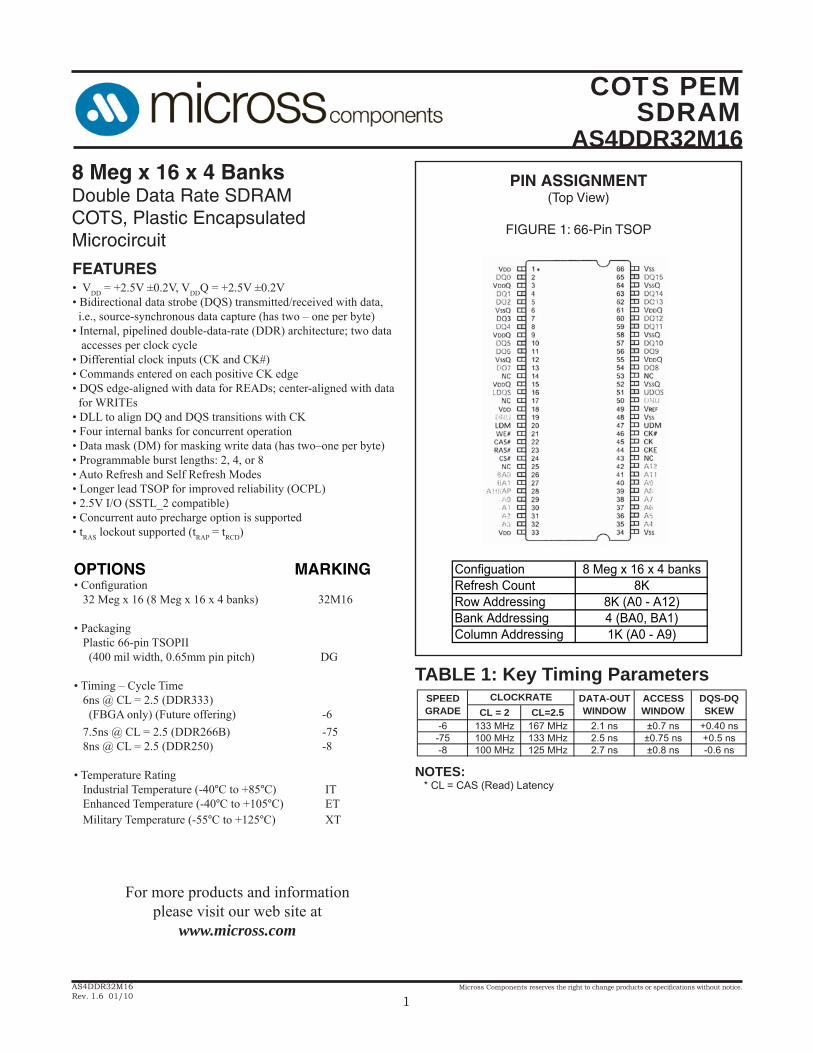
FIGURE 2: 512Mb DDR SRAM Part NumberEXAMPLE: AS4DDR32M16DG-75/IT
- /AS4DDR 32M16 Package Speed Temperature
TEMPERATUREPACKAGING Industrial Temperature IT
400 mil TSOP DG Enhanced Temperature ETMilitary Temperature XT
SPEED-6 tCK = 6ns, CL = 2.5
-75 tCK = 7.5ns, CL = 2.5
-8 tCK = 8ns, CL = 2.5
COTS PEMSDRAM
AS4DDR32M16
Micross Components reserves the right to change products or specifi cations without notice.
3AS4DDR32M16Rev. 1.6 01/10
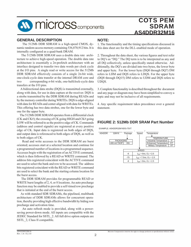
FIGURE 3: FUNCTIONAL BLOCK DIAGRAM 32 Meg x 16
COTS PEMSDRAM
AS4DDR32M16
Micross Components reserves the right to change products or specifi cations without notice.
4AS4DDR32M16Rev. 1.6 01/10
FUNCTIONAL DESCRIPTION The 512Mb DDR SDRAM is a high-speed CMOS, dy-namic random-access memory containing 536,870,912 bits. The 512Mb DDR SDRAM is internally confi gured as a quad-bank DRAM. The 512Mb DDR SDRAM uses a double data rate architecture to achieve high-speed operation. The double data rate architecture is essentially a 2n-prefetch architecture, with an interface designed to transfer two data words per clock cycle at the I/O pins. A single read or write access for the 512Mb DDR SDRAM consists of a single 2n-bit wide, one-clock-cycle data transfer at the internal DRAM core and two corresponding n-bit wide, one-half-clock-cycle data transfers at the I/O pins. Read and write accesses to the DDR SDRAM are burst oriented; accesses start at a selected location and continue for a programmed number of locations in a programmed sequence. Accesses begin with the registration of an ACTIVE command, which is then followed by a READ or WRITE command. The address bits registered coincident with the ACTIVE com-mandare used to select the bank and row to be accessed (BA0, BA1 select the bank; A0-A12 select the row). The address bits reg-istered coincident with the READ or WRITE command are used to select the starting column location for the burst access. Prior to normal operation, the DDR SDRAM must be initialized. The following sections provide detailed information covering device initialization, register defi nition, command descriptions, and device operation.
INITIALIZATION DDR SDRAMs must be powered up and initialized in a predefi ned manner. Operational procedures other than those specifi ed may result in undefi ned operation. Power must fi rst be applied to VDD and VDDQ simultaneously, and then to VREF (and to the system VTT). VTT must be applied after VDDQ to avoid device latch-up, which may cause permanent damage to the device. VREF can be applied any time after VDDQ but is expected to be nominally coincident with VTT. Except for CKE, inputs are not recognized as valid until after VREF is applied. CKE is an SSTL_2 input but will detect an LVCMOS LOW level after VDD is applied. After CKE passes through VIH, it will transition to a SSTL 2 signal and remain as such until power is cycled. Maintaining an LVCMOS LOW level on CKE during power-up is required to ensure that the DQ and DQS outputs will be in the High-Z state, where they will remain untildriven in normal operation (by a read access). After all power supply and reference voltages are stable, and the clock is stable, the DDR SDRAM requires a 200μs delay prior to applying an executable command.
Once the 200μs delay has been satisfi ed, a DESELECT or NOP command should be applied, and CKE should be brought HIGH. Following the NOP command, a PRECHARGE ALL command should be applied. Next a LOAD MODE REGISTER command should be issued for the extended mode register (BA1LOW and BA0 HIGH) to enable the DLL, followed by another LOAD MODE REGISTER command to the mode register (BA0/BA1 both LOW) to reset the DLL and to program the operating parameters. Two-hundred clock cycles are required between the DLL reset and any READ command. A PRE-CHARGE ALL command should then be applied, placing the device in the all banks idle state. Once in the idle state, two AUTO REFRESH cycles must be performed (tRFC must be satisfi ed.) Additionally, a LOAD MODE REGISTER command for the mode register with the reset DLL bit deactivated (i.e., to program operating parameters without resetting the DLL) is required. Following these requirements, the DDR SDRAM is ready for normal operation.
REGISTER DEFINITION
Mode Register
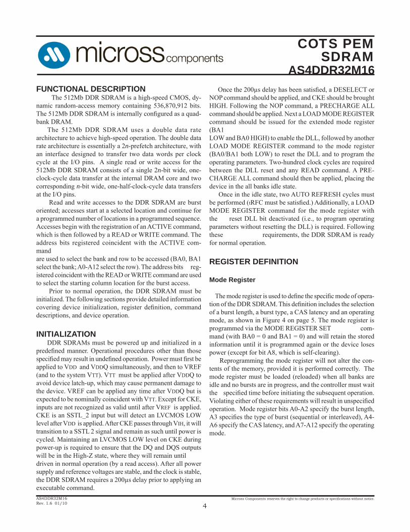
The mode register is used to defi ne the specifi c mode of opera-tion of the DDR SDRAM. This defi nition includes the selection of a burst length, a burst type, a CAS latency and an operating mode, as shown in Figure 4 on page 5. The mode register is programmed via the MODE REGISTER SET com-mand (with BA0 = 0 and BA1 = 0) and will retain the stored information until it is programmed again or the device loses power (except for bit A8, which is self-clearing). Reprogramming the mode register will not alter the con-tents of the memory, provided it is performed correctly. The mode register must be loaded (reloaded) when all banks are idle and no bursts are in progress, and the controller must wait the specifi ed time before initiating the subsequent operation. Violating either of these requirements will result in unspecifi ed operation. Mode register bits A0-A2 specify the burst length, A3 specifi es the type of burst (sequential or interleaved), A4-A6 specify the CAS latency, and A7-A12 specify the operating mode.
COTS PEMSDRAM
AS4DDR32M16
Micross Components reserves the right to change products or specifi cations without notice.
5AS4DDR32M16Rev. 1.6 01/10
BURST LENGTH Read and write accesses to the DDR SDRAM are burst oriented, with the burst length being programmable, as shown in Figure 4. The burst length determines the maximum number of column locations that can be accessed for a given READ or WRITE command.Burst lengths of 2, 4, or 8 locations are available for both the sequential and the interleaved burst types. Reserved states should not be used, as unknown operation or incompatibility with future versions may result. When a READ or WRITE command is issued, a block of columns equal to the burst length is effectively selected. All accesses for that burst take place within this block, meaning that the burst will wrap within the block if a boundary is reached. The block is uniquely selected by A1-Ai when the burst length is set to two, by A2-Ai when the burst length is set to four and by A3-Ai when the burst length is set to eight (where Ai is themost signifi cant column address bit for a given confi guration). The remaining (least signifi cant) address bit(s) is (are) used to select the starting location within the block. The programmed burst length applies to both READ and WRITE bursts.
BURST TYPE Accesses within a given burst may be programmed to be either sequential or interleaved; this is referred to as the burst type and is selected via bit M3. The ordering of accesses within a burst is determined by the burst length, the burst type and the starting column address, as shown in Table 2, Burst
FIGURE 4: Mode Register Defi nition
TABLE 2: BURST DEFINITION
TYPE = SEQUENTIAL
TYPE = INTERLEAVED
A00 0-1 0-11 1-0 1-0
A1 A00 0 0-1-2-3 0-1-2-30 1 1-2-3-0 1-0-3-21 0 2-3-0-1 2-3-0-11 1 3-0-1-2 3-2-1-0
A2 A1 A00 0 0 0-1-2-3-4-5-6-7 0-1-2-3-4-5-6-70 0 1 1-2-3-4-5-6-7-0 1-0-3-2-5-4-7-60 1 0 2-3-4-5-6-7-0-1 2-3-0-1-6-7-4-50 1 1 3-4-5-6-7-0-1-2 3-2-1-0-7-6-5-41 0 0 4-5-6-7-0-1-2-3 4-5-6-7-0-1-2-31 0 1 5-6-7-0-1-2-3-4 5-4-7-6-1-0-3-21 1 0 6-7-0-1-2-3-4-5 6-7-4-5-2-3-0-11 1 1 7-0-1-2-3-4-5-6 7-6-5-4-3-2-1-0
4
8
STARTINGCOLUMNADDRESS
ORDER OF ACCESSWITHIN A BURSTBURST
LENGTH
2
NOTES: 1. Whenever a boundary of the block is reached within a given sequence in Table 2, the following access wraps within the block.2. For a burst length of two, A1 - Ai select the two-data-element block; A0 selects the fi rst access within the block.3. For a burst length of four, A2 - Ai select the four-data-element block; A0-A1 select the fi rst access within the block.4. For a burst length of eight, A3 - Ai select the eight-data-element block; A0-A2 select the fi rst access within the block.
COTS PEMSDRAM
AS4DDR32M16
Micross Components reserves the right to change products or specifi cations without notice.
6AS4DDR32M16Rev. 1.6 01/10
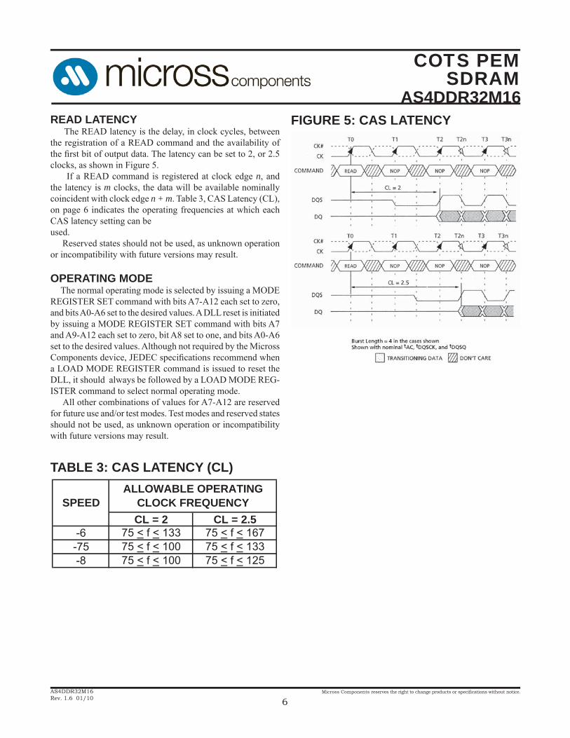
READ LATENCY The READ latency is the delay, in clock cycles, between the registration of a READ command and the availability of the fi rst bit of output data. The latency can be set to 2, or 2.5 clocks, as shown in Figure 5. If a READ command is registered at clock edge n, and the latency is m clocks, the data will be available nominally coincident with clock edge n + m. Table 3, CAS Latency (CL), on page 6 indicates the operating frequencies at which each CAS latency setting can beused. Reserved states should not be used, as unknown operation or incompatibility with future versions may result.
OPERATING MODE The normal operating mode is selected by issuing a MODE REGISTER SET command with bits A7-A12 each set to zero, and bits A0-A6 set to the desired values. A DLL reset is initiated by issuing a MODE REGISTER SET command with bits A7 and A9-A12 each set to zero, bit A8 set to one, and bits A0-A6 set to the desired values. Although not required by the Micross Components device, JEDEC specifi cations recommend when a LOAD MODE REGISTER command is issued to reset the DLL, it should always be followed by a LOAD MODE REG-ISTER command to select normal operating mode. All other combinations of values for A7-A12 are reserved for future use and/or test modes. Test modes and reserved states should not be used, as unknown operation or incompatibility with future versions may result.
FIGURE 5: CAS LATENCY
TABLE 3: CAS LATENCY (CL)
SPEEDALLOWABLE OPERATING
CLOCK FREQUENCYCL = 2 CL = 2.5
-6 75 < f < 133 75 < f < 167-75 75 < f < 100 75 < f < 133-8 75 < f < 100 75 < f < 125
COTS PEMSDRAM
AS4DDR32M16
Micross Components reserves the right to change products or specifi cations without notice.
7AS4DDR32M16Rev. 1.6 01/10
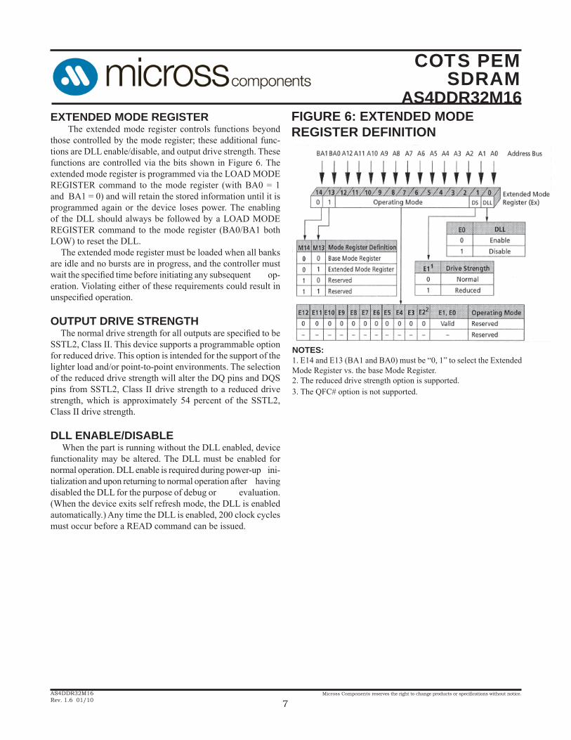
EXTENDED MODE REGISTER The extended mode register controls functions beyond those controlled by the mode register; these additional func-tions are DLL enable/disable, and output drive strength. These functions are controlled via the bits shown in Figure 6. The extended mode register is programmed via the LOAD MODE REGISTER command to the mode register (with BA0 = 1 and BA1 = 0) and will retain the stored information until it is programmed again or the device loses power. The enabling of the DLL should always be followed by a LOAD MODE REGISTER command to the mode register (BA0/BA1 both LOW) to reset the DLL. The extended mode register must be loaded when all banks are idle and no bursts are in progress, and the controller must wait the specifi ed time before initiating any subsequent op-eration. Violating either of these requirements could result in unspecifi ed operation.
OUTPUT DRIVE STRENGTH The normal drive strength for all outputs are specifi ed to be SSTL2, Class II. This device supports a programmable option for reduced drive. This option is intended for the support of the lighter load and/or point-to-point environments. The selection of the reduced drive strength will alter the DQ pins and DQS pins from SSTL2, Class II drive strength to a reduced drive strength, which is approximately 54 percent of the SSTL2, Class II drive strength.
DLL ENABLE/DISABLE When the part is running without the DLL enabled, device functionality may be altered. The DLL must be enabled for normal operation. DLL enable is required during power-up ini-tialization and upon returning to normal operation after having disabled the DLL for the purpose of debug or evaluation. (When the device exits self refresh mode, the DLL is enabled automatically.) Any time the DLL is enabled, 200 clock cycles must occur before a READ command can be issued.
NOTES: 1. E14 and E13 (BA1 and BA0) must be “0, 1” to select the Extended Mode Register vs. the base Mode Register.2. The reduced drive strength option is supported.3. The QFC# option is not supported.
FIGURE 6: EXTENDED MODE REGISTER DEFINITION
COTS PEMSDRAM
AS4DDR32M16
Micross Components reserves the right to change products or specifi cations without notice.
8AS4DDR32M16Rev. 1.6 01/10
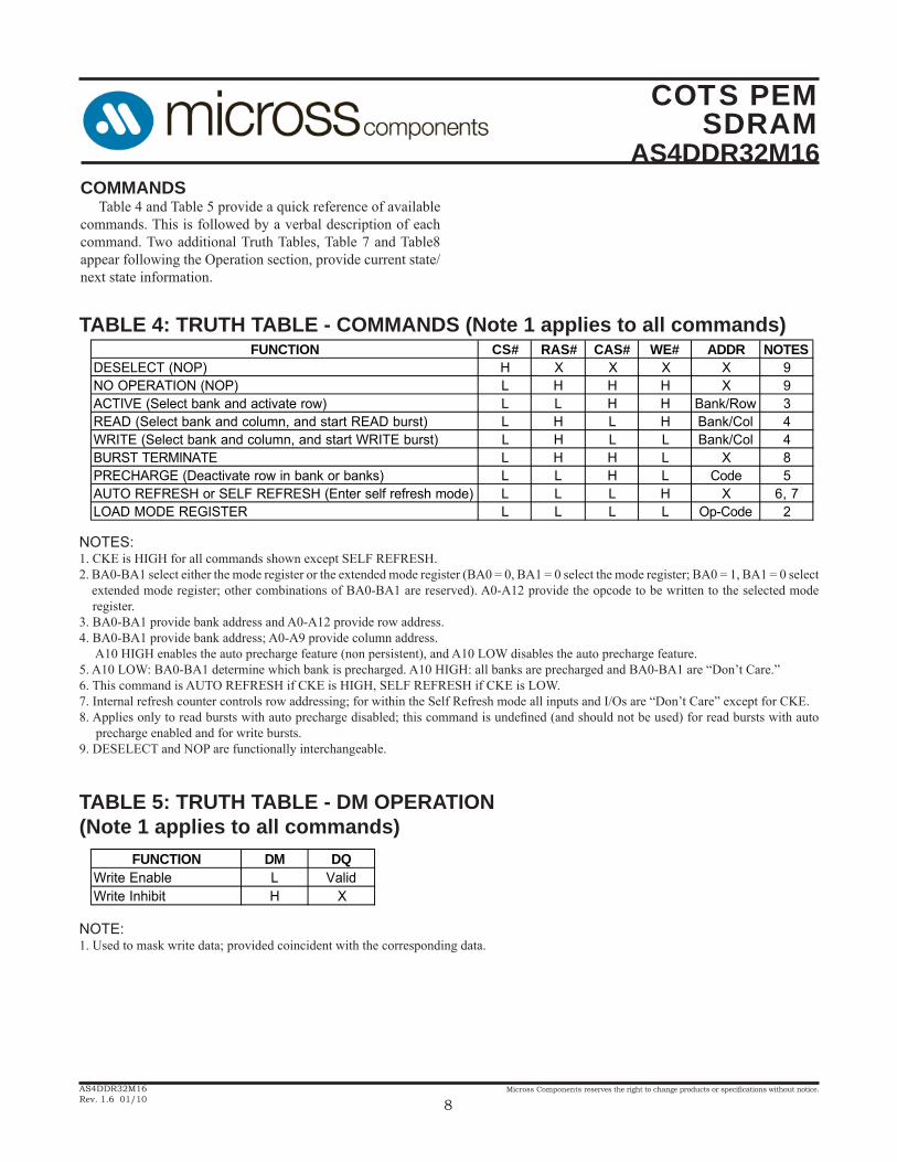
COMMANDS Table 4 and Table 5 provide a quick reference of available commands. This is followed by a verbal description of each command. Two additional Truth Tables, Table 7 and Table8 appear following the Operation section, provide current state/next state information.
NOTES:1. CKE is HIGH for all commands shown except SELF REFRESH.2. BA0-BA1 select either the mode register or the extended mode register (BA0 = 0, BA1 = 0 select the mode register; BA0 = 1, BA1 = 0 select extended mode register; other combinations of BA0-BA1 are reserved). A0-A12 provide the opcode to be written to the selected mode register.3. BA0-BA1 provide bank address and A0-A12 provide row address.4. BA0-BA1 provide bank address; A0-A9 provide column address. A10 HIGH enables the auto precharge feature (non persistent), and A10 LOW disables the auto precharge feature.5. A10 LOW: BA0-BA1 determine which bank is precharged. A10 HIGH: all banks are precharged and BA0-BA1 are “Don’t Care.”6. This command is AUTO REFRESH if CKE is HIGH, SELF REFRESH if CKE is LOW.7. Internal refresh counter controls row addressing; for within the Self Refresh mode all inputs and I/Os are “Don’t Care” except for CKE.8. Applies only to read bursts with auto precharge disabled; this command is undefi ned (and should not be used) for read bursts with auto precharge enabled and for write bursts.9. DESELECT and NOP are functionally interchangeable.
NOTE:1. Used to mask write data; provided coincident with the corresponding data.
TABLE 4: TRUTH TABLE - COMMANDS (Note 1 applies to all commands)FUNCTION CS# RAS# CAS# WE# ADDR NOTES
DESELECT (NOP) H X X X X 9NO OPERATION (NOP) L H H H X 9ACTIVE (Select bank and activate row) L L H H Bank/Row 3READ (Select bank and column, and start READ burst) L H L H Bank/Col 4WRITE (Select bank and column, and start WRITE burst) L H L L Bank/Col 4BURST TERMINATE L H H L X 8PRECHARGE (Deactivate row in bank or banks) L L H L Code 5AUTO REFRESH or SELF REFRESH (Enter self refresh mode) L L L H X 6, 7LOAD MODE REGISTER L L L L Op-Code 2
TABLE 5: TRUTH TABLE - DM OPERATION (Note 1 applies to all commands)
FUNCTION DM DQWrite Enable L ValidWrite Inhibit H X
COTS PEMSDRAM
AS4DDR32M16
Micross Components reserves the right to change products or specifi cations without notice.
9AS4DDR32M16Rev. 1.6 01/10
DESELECT The DESELECT function (CS# HIGH) prevents new commands from being executed by the DDR SDRAM. The DDR SDRAM is effectively deselected. Operations already in progress are not affected.
NO OPERATION (NOP) The NO OPERATION (NOP) command is used to instruct the selected DDR SDRAM to perform a NOP (CS# is LOW with RAS#, CAS#, and WE# are HIGH). This prevents unwanted commands from being registered during idle or wait states. Operations already in progress are not affected.
LOAD MODE REGISTER The mode registers are loaded via inputs A0–A12. See mode register descriptions in the Register Defi nition section. The LOAD MODE REGISTER command can only be issued when all banks are idle, and a subsequent executable command cannot be issued until tMRD is met.
ACTIVE The ACTIVE command is used to open (or activate) a row in a particular bank for a subsequent access. The value on the BA0, BA1 inputs selects the bank, and the address provided on inputs A0–A12 selects the row. This row remains active (or open) for accesses until a precharge command is issued to that bank. A precharge command must be issued before opening a different row in the same bank.
READ The READ command is used to initiate a burst read access to an active row. The value on the BA0, BA1 inputs selects the bank, and the address provided on inputs A0–A9 selects the starting column location. The value on input A10 determines whether or not auto precharge is used. If auto precharge is selected, the row being accessed will be precharged at the end of the READ burst; if auto precharge is not selected, the row will remain open for subsequent accesses.
WRITE The WRITE command is used to initiate a burst write access to an active row. The value on the BA0, BA1 inputs selects the bank, and the address provided on inputs A0–A9 selects the starting column location. The value on input A10 determines whether or not auto precharge is used. If auto precharge is selected, the row being accessed will be precharged at the end of the WRITE burst; if auto precharge is not selected, the row
will remain open for subsequent accesses. Input data appearing on the DQ is written to the memory arraysubject to the DM input logic level appearing coincident with the data. If a given DM signal is registered LOW, the cor-responding data will be written to memory; if the DM signal is registered HIGH, the corresponding data inputs will be ig-nored, and a WRITE will not be executed to that byte/column location.
PRECHARGE The PRECHARGE command is used to deactivate the open row in a particular bank or the open row in all banks. The bank(s) will be available for a subsequent row access a specifi ed time (tRP) after the precharge command is issued. Except in the case of concurrent auto precharge, where a READ or WRITE command to a different bank is allowed as long as it does not interrupt the data transfer in the current bank and does not vio-late any other timing parameters. Input A10 determines whether one or all banks are to be precharged, and in the case where only one bank is to be precharged, inputs BA0, BA1 select the bank. Otherwise BA0, BA1 are treated as “Don’t Care.” Once a bank has been precharged, it is in the idle state and must be activated prior to any READ or WRITE commandsbeing issued to that bank. A PRECHARGE command will be treated as a NOP if there is no open row in that bank (idle state), or if the previously open row is already in the process of precharging.
AUTO PRECHARGE Auto precharge is a feature which performs the same individual-bank precharge function described above, but without requiring an explicit command. This is accomplished by using A10 to enable auto precharge in conjunction with a specifi c READ or WRITE command. A precharge of the bank/row that is addressed with the READ or WRITE command is automatically performed upon completion of the READ or WRITE burst. Auto precharge is nonpersistent in that it is either enabled or disabled for each individual Read or Write command. This device supports concurrent auto precharge if the command to the other bank does not interrupt the data transfer to the current bank. Auto precharge ensures that the precharge is initiated at the earliest valid stage within a burst. This “earliest valid stage” is determined as if an explicit PRECHARGE command was issued at the earliest possible time, without violating tRAS (MIN), as described for each burst type in the Operation section of this data sheet. The user must not issue another command to the same bank until the precharge time (tRP) is completed.
COTS PEMSDRAM
AS4DDR32M16
Micross Components reserves the right to change products or specifi cations without notice.
10AS4DDR32M16Rev. 1.6 01/10
BURST TERMINATE The BURST TERMINATE command is used to truncate read bursts (with auto precharge disabled). The most recently registered READ command prior to the BURST TERMINATE command will be truncated, as shown in the Operation section of this data sheet. The open page which the READ burst was terminated from remains open.
AUTO REFRESH AUTO REFRESH is used during normal operation of the DDR SDRAM and is analogous to CAS#-BEFORE RAS# (CBR) refresh in FPM/EDO DRAMs. This command is non-persistent, so it must be issued each time a refresh is required. All banks must be idle before an AUTO REFRESH command is issued. The addressing is generated by the internal refresh controller. This makes the address bits a “Don’t Care” during an AUTO REFRESH command. The 512Mb DDR SDRAM requires AUTO REFRESH cycles at an average interval of 7.8125μs (maximum). To allow for improved efficiency in scheduling and switching between tasks, some fl exibility in the absolute refresh interval is provided. A maximum of eight AUTO REFRESH commands can be posted to any given DDR SDRAM, mean-ing that the maximum absolute interval between any AUTO REFRESH command and the next AUTO REFRESH com-mand is 9 x 7.8125μs (70.3μs). Note the JEDEC specifi ca-tions only allows 8 x 7.8125μs, thus the Micross Components specifi cation exceeds the JEDEC requirement by one clock. This maximum absolute interval is to allow future support for DLL updates internal to the DDR SDRAM to be restricted to AUTO REFRESH cycles, without allowing excessive drift in tAC between updates. Although not a JEDEC requirement, to provide for future functionality features, CKE must be active (High) during the AUTO REFRESH period. The AUTO REFRESH period begins when the AUTO REFRESH command is registered and ends tRFC later.
SELF REFRESH The SELF REFRESH command can be used to retain data in the DDR SDRAM, even if the rest of the system is powered down. When in the self refresh mode, the DDR SDRAM retains data without external clocking. The SELF REFRESH command is initiated like an AUTO REFRESH command except CKE is disabled (LOW). The DLL is automatically disabled upon entering SELF REFRESH and is automatically enabled upon exiting SELF REFRESH (A DLL reset and 200 clock cycles must then occur before a READ command can be issued). Input signals except CKE are “Don’t Care” during SELF
REFRESH. VREF voltage is also required for the full duration of SELF REFRESH. The procedure for exiting self refresh requires a sequence of commands. First, CK and CK# must be stable prior to CKE going back HIGH. Once CKE is HIGH, the DDR SDRAM must have NOP commands issued for tXSNR because time is required for the completion of any internal refresh in prog-ress. A simple algorithm for meeting both refresh and DLL requirements is to apply NOPs for tXSNR time, then a DLL Reset and NOPs for 200 additional clock cycles before apply-ing any other command.
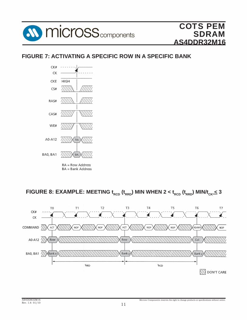
BANK/ROW ACTIVATION Before any READ or WRITE commands can be issued to a bank within the DDR SDRAM, a row in that bank must be “opened.” This is accomplished via the ACTIVE command, which selects both the bank and the row to be activated, as shown in Figure 7. After a row is opened with an ACTIVE command, a READ or WRITE command may be issued to that row, subject to the tRCD specifi cation. tRCD (MIN) should be divided by the clock period and rounded up to the next whole number to determine the earliest clock edge after the ACTIVE command on which a READ or WRITE command can be entered. For example, a tRCD specifi cation of 20ns with a 133 MHz clock (7.5ns period) results in 2.7 clocks rounded to 3. This is refl ected in Figure 8, which covers any case where 2 <tRCD (MIN)/tCK < 3. (Figure 8 also shows the same case for tRCD; the same procedure is used to convert other specifi cation limits from time units to clock cycles). A subsequent ACTIVE command to a different row in the same bank can only be issued after the previous active row has been “closed” (precharged). The minimum time interval between successive ACTIVE commands to the same bank is defi ned by tRC. A subsequent ACTIVE command to another bank can be issued while the fi rst bank is being accessed, which results in a reduction of total row-access overhead. The minimum time interval between successive ACTIVE commands to different banks is defi ned by tRRD.
COTS PEMSDRAM
AS4DDR32M16
Micross Components reserves the right to change products or specifi cations without notice.
11AS4DDR32M16Rev. 1.6 01/10
FIGURE 7: ACTIVATING A SPECIFIC ROW IN A SPECIFIC BANK
FIGURE 8: EXAMPLE: MEETING tRCD (tRRD) MIN WHEN 2 < tRCD (tRRD) MIN/tCK < 3

COTS PEMSDRAM
AS4DDR32M16
Micross Components reserves the right to change products or specifi cations without notice.
12AS4DDR32M16Rev. 1.6 01/10
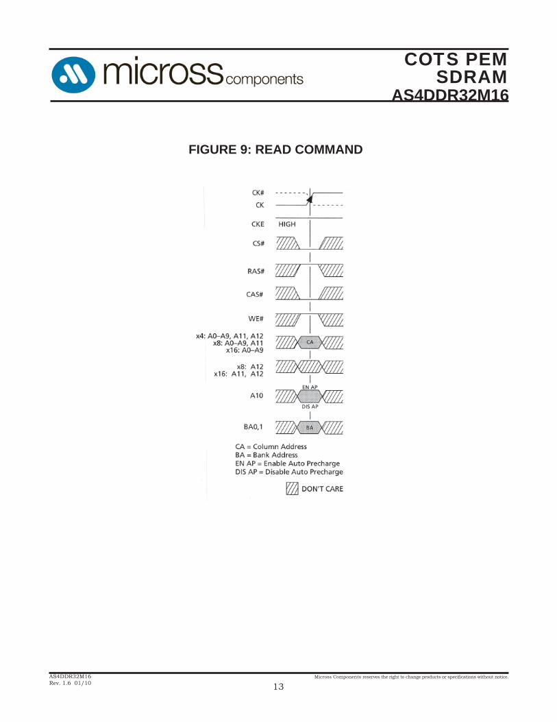
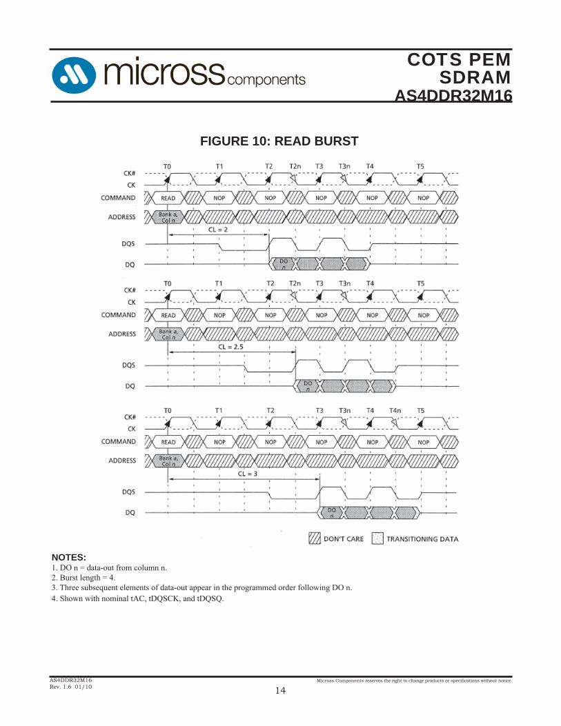
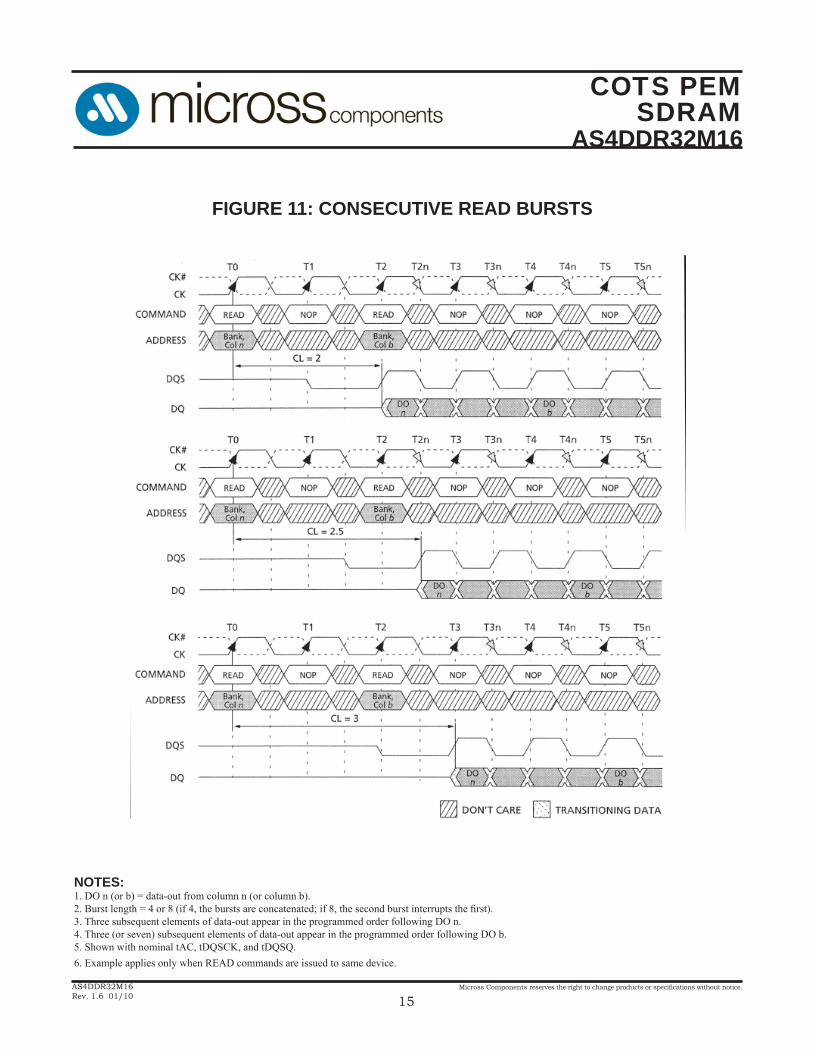
READs READ bursts are initiated with a READ command, as shown in Figure 9. The starting column and bank addresses are provided with the READ command and auto precharge is either enabled or disabled for that burst access. If auto pre-charge is enabled, the row being accessed is precharged at the completion of the burst.NOTE: For the READ commands used in the following illustrations, auto precharge is disabled. During READ bursts, the valid data-out element from the starting column address will be available following the CAS latency after the READ command. Each subsequent data-out element will be valid nominally at the next positive or negative clock edge (i.e., at the next crossing of CK and CK#). Figure 10 shows general timing for each possible CAS latency setting. DQS is driven by the DDR SDRAM along with output data. The initial LOW state on DQS is known as the read preamble; the LOW state coincident with the last data-out element is known as the read postamble. Upon completion of a burst, assuming no other commands have been initiated, the DQs will go High-Z. A detailed explanation of tDQSQ (valid data-out skew), tQH (data-out window hold), the valid data window are depicted in Figure 37. A detailed explanation of tDQSCK (DQS transition skew to CK) and tAC (data-out transition skew to CK) is depicted in Figure 38. Data from any READ burst may be concatenated with or truncated with data from a subsequent READ command. In either case, a continuous fl ow of data can be maintained. The fi rst data element from the new burst follows either the last element of a completed burst or the last desired data element of a longer burst which is being truncated. The new READ command should be issued x cycles after the fi rst READ
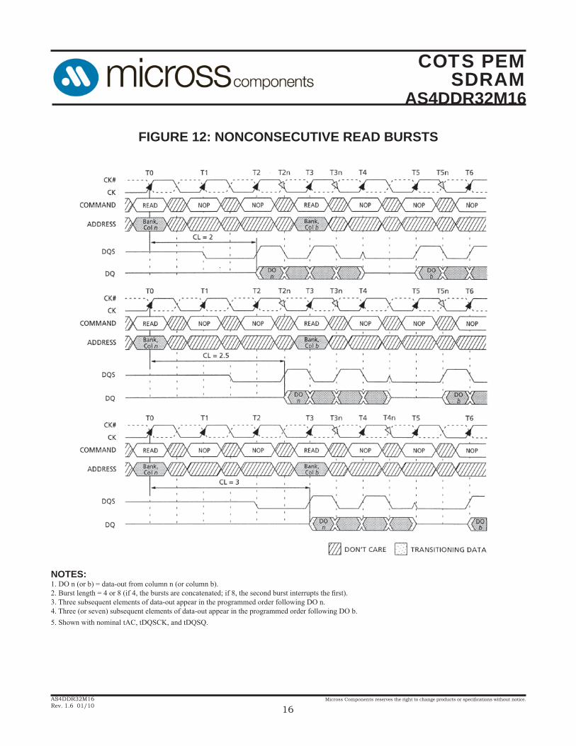
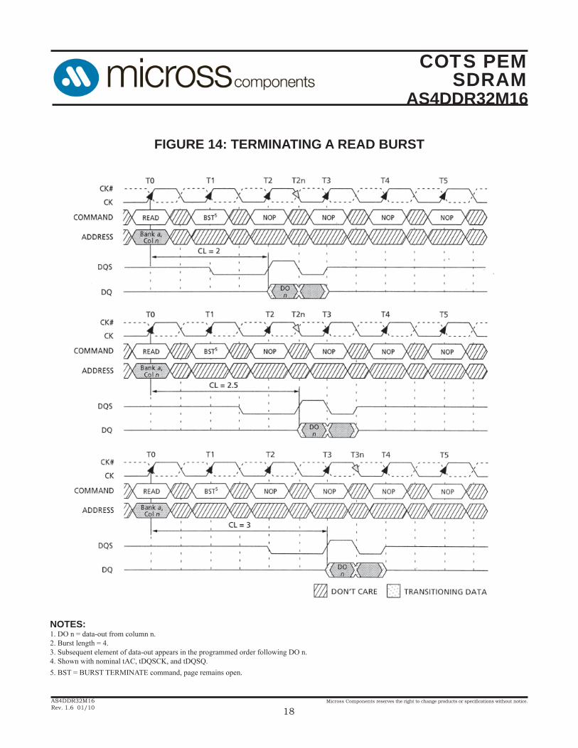
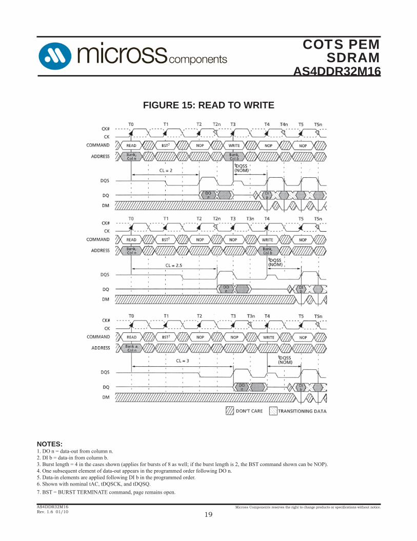
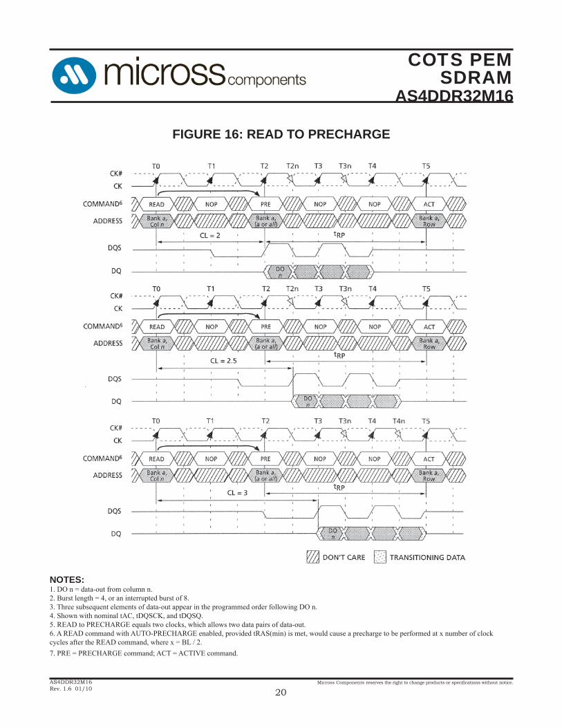
command, where x equals the number of desired data element pairs (pairs are required by the 2n-prefetch architecture). This is shown in Figure 11. A READ command can be initiated on any clock cycle following a previous READ command. Nonconsecutive read data is shown for illustration in Figure 12. Full-speed random read accesses within a page (or pages) can be performed as shown in Figure 13. Data from any READ burst may be truncated with a BURST TERMINATE command, as shown in Figure 14. The BURST TERMINATE latency is equal to the read (CAS) latency, i.e., the BURST TERMINATE command should be issued x cycles after the READ command, where x equals the number of desired data element pairs (pairs are required by the 2n-prefetcharchitecture). Data from any READ burst must be completed or trun-cated before a subsequent WRITE command can be issued. If truncation is necessary, the BURST TERMINATE command must be used, as shown in Figure 15. The tDQSS (NOM) case is shown; the tDQSS (MAX) case has a longer bus idle time. (tDQSS [MIN] and tDQSS [MAX] are defi ned in the section on WRITEs.) A READ burst may be followed by, or truncated with, a PRECHARGE command to the same bank provided that auto precharge was not activated. The PRECHARGE command should be issued x cycles after the READ command, where x equals the number of desired data element pairs (pairs are required by the 2n-prefetch architecture). This is shown in Figure 16. Following the PRECHARGE command, a subse-quent command to the same bank cannot be issued until both tRAS and tRP has been met. Note that part of the row precharge time is hidden during the access of the last data elements.
COTS PEMSDRAM
AS4DDR32M16
Micross Components reserves the right to change products or specifi cations without notice.
13AS4DDR32M16Rev. 1.6 01/10
FIGURE 9: READ COMMAND
COTS PEMSDRAM
AS4DDR32M16
Micross Components reserves the right to change products or specifi cations without notice.
14AS4DDR32M16Rev. 1.6 01/10
FIGURE 10: READ BURST
NOTES:1. DO n = data-out from column n.2. Burst length = 4.3. Three subsequent elements of data-out appear in the programmed order following DO n.4. Shown with nominal tAC, tDQSCK, and tDQSQ.
COTS PEMSDRAM
AS4DDR32M16
Micross Components reserves the right to change products or specifi cations without notice.
15AS4DDR32M16Rev. 1.6 01/10
FIGURE 11: CONSECUTIVE READ BURSTS
NOTES:1. DO n (or b) = data-out from column n (or column b).2. Burst length = 4 or 8 (if 4, the bursts are concatenated; if 8, the second burst interrupts the fi rst).3. Three subsequent elements of data-out appear in the programmed order following DO n.4. Three (or seven) subsequent elements of data-out appear in the programmed order following DO b.5. Shown with nominal tAC, tDQSCK, and tDQSQ.6. Example applies only when READ commands are issued to same device.
COTS PEMSDRAM
AS4DDR32M16
Micross Components reserves the right to change products or specifi cations without notice.
16AS4DDR32M16Rev. 1.6 01/10
FIGURE 12: NONCONSECUTIVE READ BURSTS
NOTES:1. DO n (or b) = data-out from column n (or column b).2. Burst length = 4 or 8 (if 4, the bursts are concatenated; if 8, the second burst interrupts the fi rst).3. Three subsequent elements of data-out appear in the programmed order following DO n.4. Three (or seven) subsequent elements of data-out appear in the programmed order following DO b.5. Shown with nominal tAC, tDQSCK, and tDQSQ.
COTS PEMSDRAM
AS4DDR32M16
Micross Components reserves the right to change products or specifi cations without notice.
17AS4DDR32M16Rev. 1.6 01/10
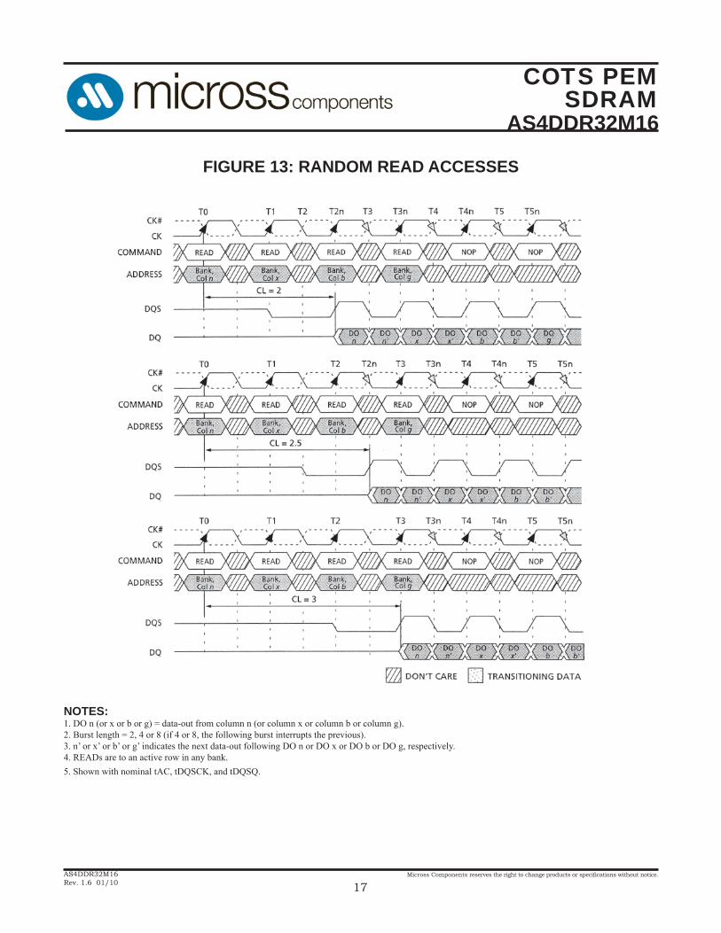
FIGURE 13: RANDOM READ ACCESSES
NOTES:1. DO n (or x or b or g) = data-out from column n (or column x or column b or column g).2. Burst length = 2, 4 or 8 (if 4 or 8, the following burst interrupts the previous).3. n’ or x’ or b’ or g’ indicates the next data-out following DO n or DO x or DO b or DO g, respectively.4. READs are to an active row in any bank.5. Shown with nominal tAC, tDQSCK, and tDQSQ.
COTS PEMSDRAM
AS4DDR32M16
Micross Components reserves the right to change products or specifi cations without notice.
18AS4DDR32M16Rev. 1.6 01/10
FIGURE 14: TERMINATING A READ BURST
NOTES:1. DO n = data-out from column n.2. Burst length = 4.3. Subsequent element of data-out appears in the programmed order following DO n.4. Shown with nominal tAC, tDQSCK, and tDQSQ.5. BST = BURST TERMINATE command, page remains open.
COTS PEMSDRAM
AS4DDR32M16
Micross Components reserves the right to change products or specifi cations without notice.
19AS4DDR32M16Rev. 1.6 01/10
FIGURE 15: READ TO WRITE
NOTES:1. DO n = data-out from column n.2. DI b = data-in from column b.3. Burst length = 4 in the cases shown (applies for bursts of 8 as well; if the burst length is 2, the BST command shown can be NOP).4. One subsequent element of data-out appears in the programmed order following DO n.5. Data-in elements are applied following DI b in the programmed order.6. Shown with nominal tAC, tDQSCK, and tDQSQ.7. BST = BURST TERMINATE command, page remains open.
COTS PEMSDRAM
AS4DDR32M16
Micross Components reserves the right to change products or specifi cations without notice.
20AS4DDR32M16Rev. 1.6 01/10
FIGURE 16: READ TO PRECHARGE
NOTES:1. DO n = data-out from column n.2. Burst length = 4, or an interrupted burst of 8.3. Three subsequent elements of data-out appear in the programmed order following DO n.4. Shown with nominal tAC, tDQSCK, and tDQSQ.5. READ to PRECHARGE equals two clocks, which allows two data pairs of data-out.6. A READ command with AUTO-PRECHARGE enabled, provided tRAS(min) is met, would cause a precharge to be performed at x number of clock cycles after the READ command, where x = BL / 2.7. PRE = PRECHARGE command; ACT = ACTIVE command.
COTS PEMSDRAM
AS4DDR32M16
Micross Components reserves the right to change products or specifi cations without notice.
21AS4DDR32M16Rev. 1.6 01/10
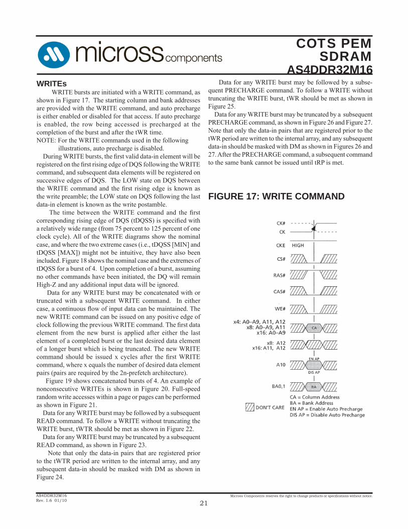
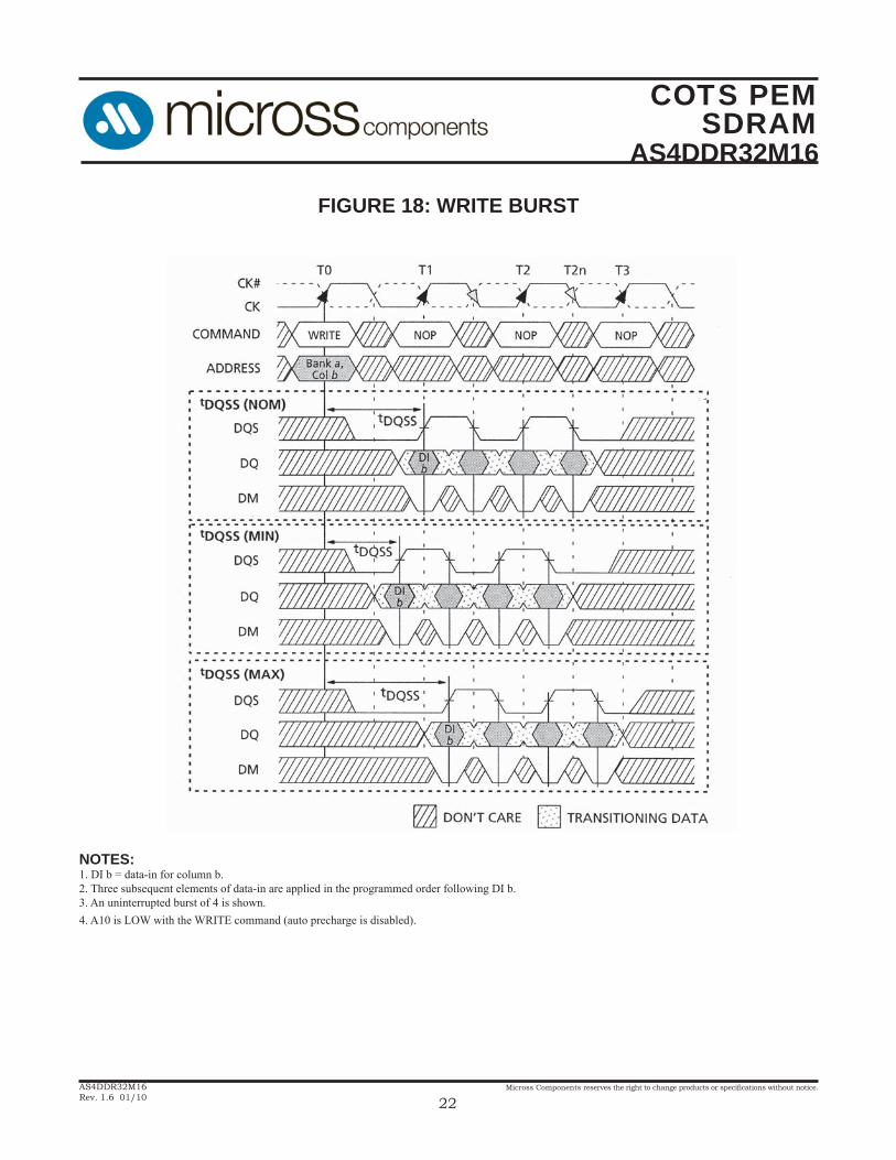
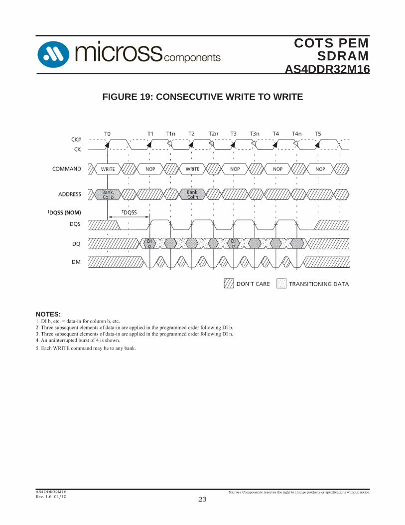
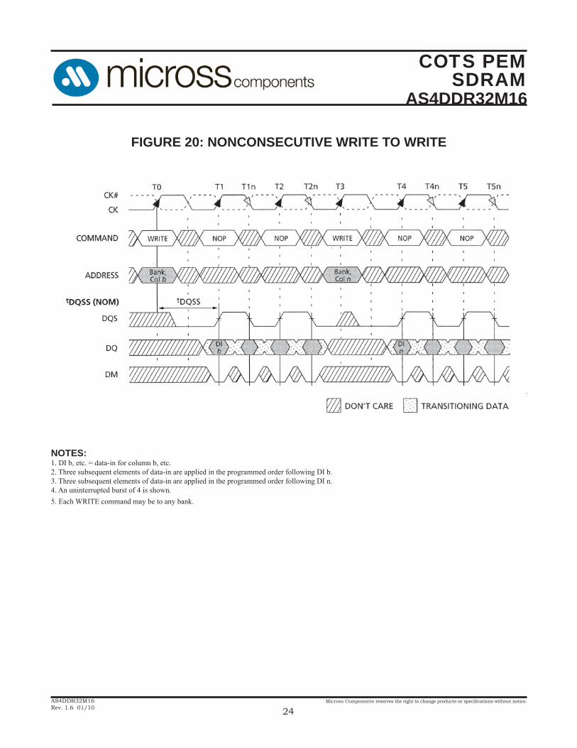
WRITEs WRITE bursts are initiated with a WRITE command, as shown in Figure 17. The starting column and bank addresses are provided with the WRITE command, and auto precharge is either enabled or disabled for that access. If auto precharge is enabled, the row being accessed is precharged at the completion of the burst and after the tWR time.NOTE: For the WRITE commands used in the following illustrations, auto precharge is disabled. During WRITE bursts, the fi rst valid data-in element will be registered on the fi rst rising edge of DQS following the WRITE command, and subsequent data elements will be registered on successive edges of DQS. The LOW state on DQS between the WRITE command and the fi rst rising edge is known as the write preamble; the LOW state on DQS following the last data-in element is known as the write postamble. The time between the WRITE command and the fi rst corresponding rising edge of DQS (tDQSS) is specifi ed with a relatively wide range (from 75 percent to 125 percent of one clock cycle). All of the WRITE diagrams show the nominal case, and where the two extreme cases (i.e., tDQSS [MIN] and tDQSS [MAX]) might not be intuitive, they have also been included. Figure 18 shows the nominal case and the extremes of tDQSS for a burst of 4. Upon completion of a burst, assuming no other commands have been initiated, the DQ will remain High-Z and any additional input data will be ignored. Data for any WRITE burst may be concatenated with or truncated with a subsequent WRITE command. In either case, a continuous fl ow of input data can be maintained. The new WRITE command can be issued on any positive edge of clock following the previous WRITE command. The fi rst data element from the new burst is applied after either the last element of a completed burst or the last desired data element of a longer burst which is being truncated. The new WRITE command should be issued x cycles after the fi rst WRITE command, where x equals the number of desired data element pairs (pairs are required by the 2n-prefetch architecture). Figure 19 shows concatenated bursts of 4. An example of nonconsecutive WRITEs is shown in Figure 20. Full-speed random write accesses within a page or pages can be performed as shown in Figure 21. Data for any WRITE burst may be followed by a subsequent READ command. To follow a WRITE without truncating the WRITE burst, tWTR should be met as shown in Figure 22. Data for any WRITE burst may be truncated by a subsequent READ command, as shown in Figure 23. Note that only the data-in pairs that are registered prior to the tWTR period are written to the internal array, and any subsequent data-in should be masked with DM as shown in Figure 24.
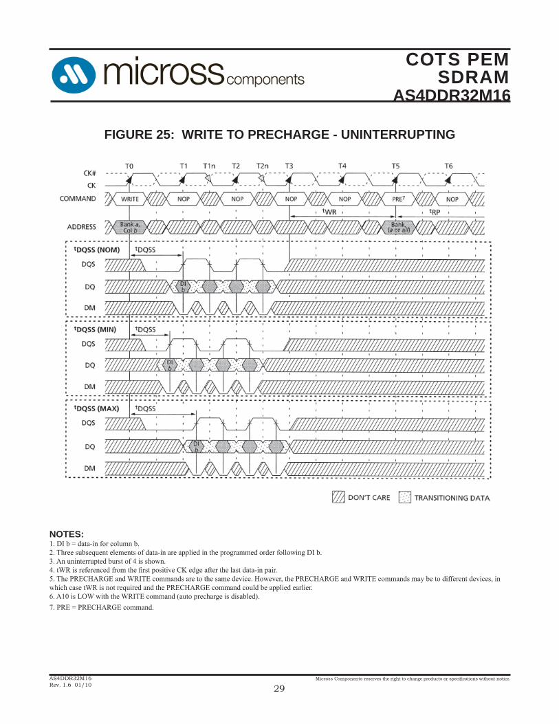
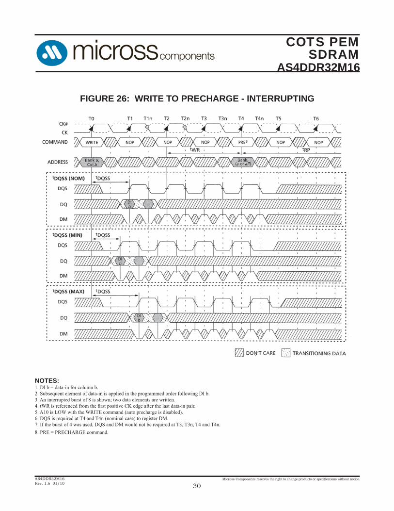
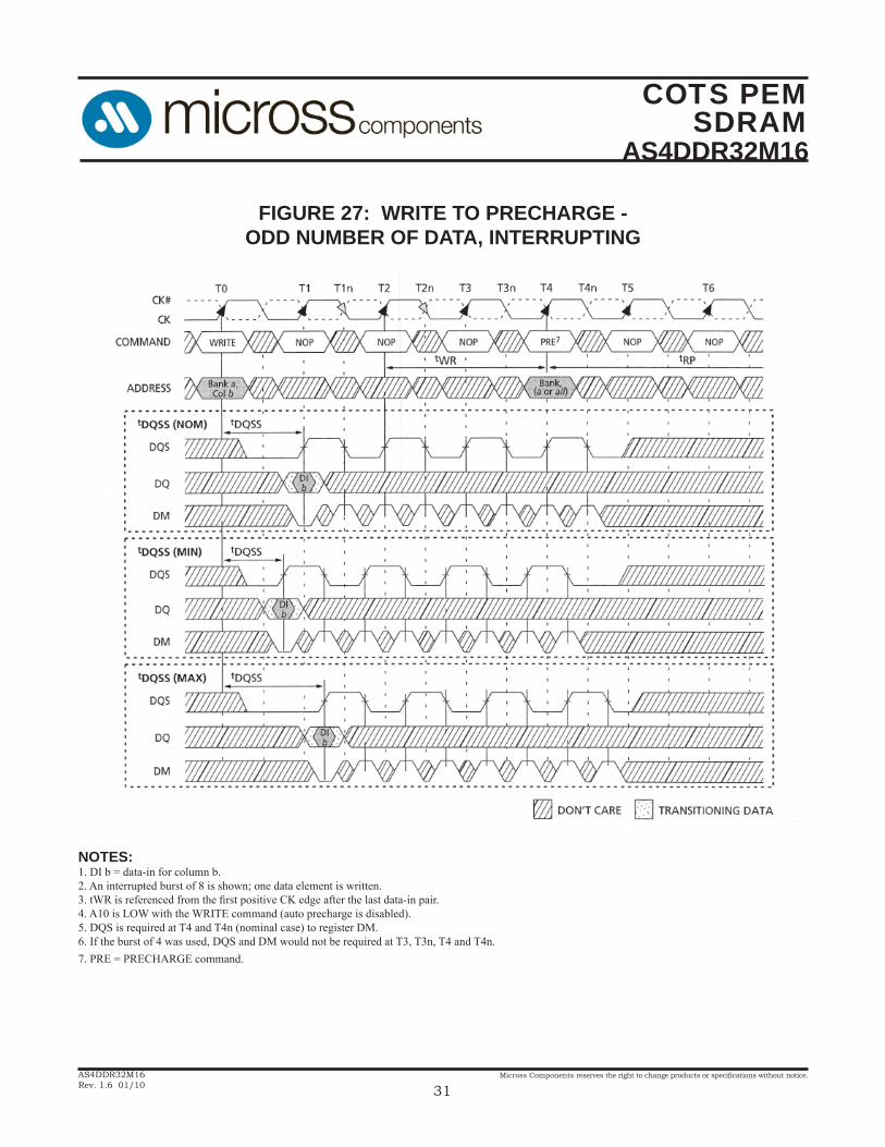
Data for any WRITE burst may be followed by a subse-quent PRECHARGE command. To follow a WRITE without truncating the WRITE burst, tWR should be met as shown in Figure 25. Data for any WRITE burst may be truncated by a subsequent PRECHARGE command, as shown in Figure 26 and Figure 27. Note that only the data-in pairs that are registered prior to the tWR period are written to the internal array, and any subsequent data-in should be masked with DM as shown in Figures 26 and 27. After the PRECHARGE command, a subsequent command to the same bank cannot be issued until tRP is met.
FIGURE 17: WRITE COMMAND
COTS PEMSDRAM
AS4DDR32M16
Micross Components reserves the right to change products or specifi cations without notice.
22AS4DDR32M16Rev. 1.6 01/10
FIGURE 18: WRITE BURST
NOTES:1. DI b = data-in for column b.2. Three subsequent elements of data-in are applied in the programmed order following DI b.3. An uninterrupted burst of 4 is shown.4. A10 is LOW with the WRITE command (auto precharge is disabled).
COTS PEMSDRAM
AS4DDR32M16
Micross Components reserves the right to change products or specifi cations without notice.
23AS4DDR32M16Rev. 1.6 01/10
FIGURE 19: CONSECUTIVE WRITE TO WRITE
NOTES:1. DI b, etc. = data-in for column b, etc.2. Three subsequent elements of data-in are applied in the programmed order following DI b.3. Three subsequent elements of data-in are applied in the programmed order following DI n.4. An uninterrupted burst of 4 is shown.5. Each WRITE command may be to any bank.
COTS PEMSDRAM
AS4DDR32M16
Micross Components reserves the right to change products or specifi cations without notice.
24AS4DDR32M16Rev. 1.6 01/10
FIGURE 20: NONCONSECUTIVE WRITE TO WRITE
NOTES:1. DI b, etc. = data-in for column b, etc.2. Three subsequent elements of data-in are applied in the programmed order following DI b.3. Three subsequent elements of data-in are applied in the programmed order following DI n.4. An uninterrupted burst of 4 is shown.5. Each WRITE command may be to any bank.
COTS PEMSDRAM
AS4DDR32M16
Micross Components reserves the right to change products or specifi cations without notice.
25AS4DDR32M16Rev. 1.6 01/10
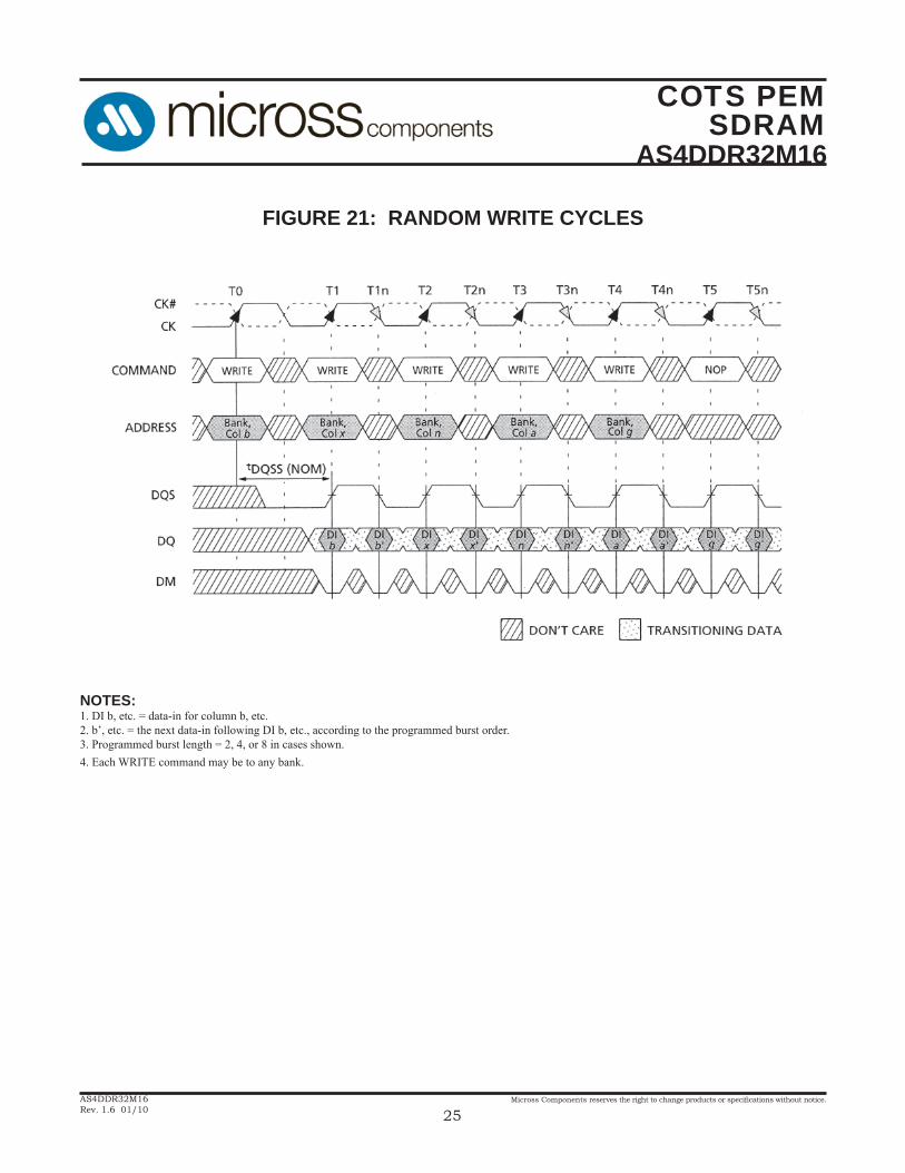
FIGURE 21: RANDOM WRITE CYCLES
NOTES:1. DI b, etc. = data-in for column b, etc.2. b’, etc. = the next data-in following DI b, etc., according to the programmed burst order.3. Programmed burst length = 2, 4, or 8 in cases shown.4. Each WRITE command may be to any bank.
COTS PEMSDRAM
AS4DDR32M16
Micross Components reserves the right to change products or specifi cations without notice.
26AS4DDR32M16Rev. 1.6 01/10
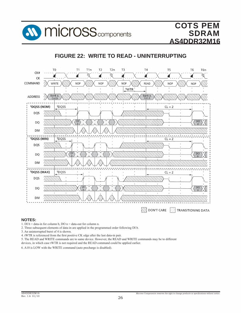
FIGURE 22: WRITE TO READ - UNINTERRUPTING
NOTES:1. DI b = data-in for column b, DO n = data-out for column n.2. Three subsequent elements of data-in are applied in the programmed order following DI b.3. An uninterrupted burst of 4 is shown.4. tWTR is referenced from the fi rst positive CK edge after the last data-in pair.5. The READ and WRITE commands are to same device. However, the READ and WRITE commands may be to differentdevices, in which case tWTR is not required and the READ command could be applied earlier.6. A10 is LOW with the WRITE command (auto precharge is disabled).
COTS PEMSDRAM
AS4DDR32M16
Micross Components reserves the right to change products or specifi cations without notice.
27AS4DDR32M16Rev. 1.6 01/10
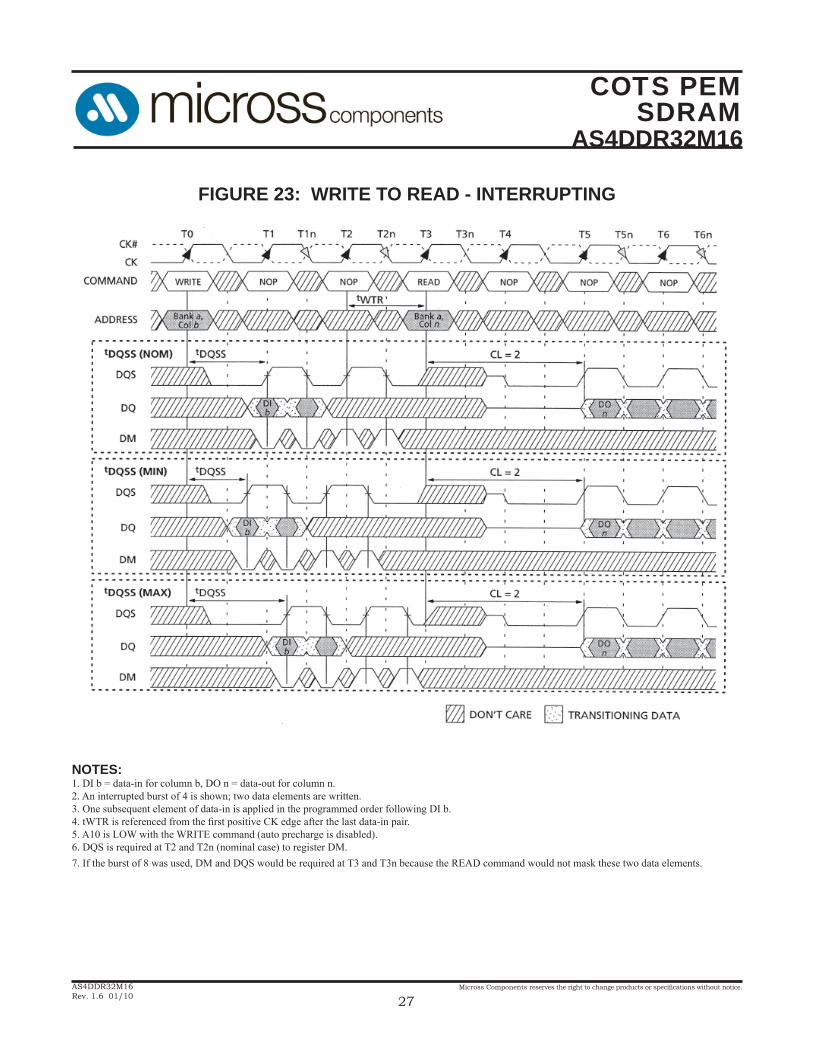
FIGURE 23: WRITE TO READ - INTERRUPTING
NOTES:1. DI b = data-in for column b, DO n = data-out for column n.2. An interrupted burst of 4 is shown; two data elements are written.3. One subsequent element of data-in is applied in the programmed order following DI b.4. tWTR is referenced from the fi rst positive CK edge after the last data-in pair.5. A10 is LOW with the WRITE command (auto precharge is disabled).6. DQS is required at T2 and T2n (nominal case) to register DM.7. If the burst of 8 was used, DM and DQS would be required at T3 and T3n because the READ command would not mask these two data elements.
COTS PEMSDRAM
AS4DDR32M16
Micross Components reserves the right to change products or specifi cations without notice.
28AS4DDR32M16Rev. 1.6 01/10
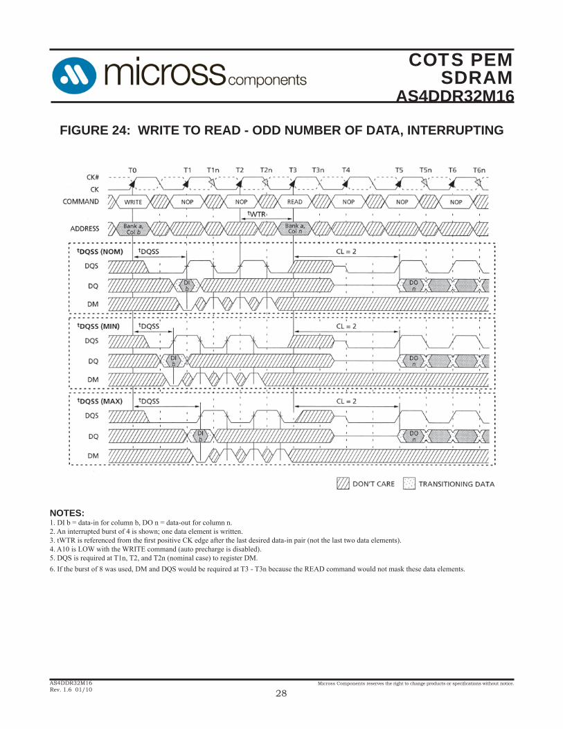
FIGURE 24: WRITE TO READ - ODD NUMBER OF DATA, INTERRUPTING
NOTES:1. DI b = data-in for column b, DO n = data-out for column n.2. An interrupted burst of 4 is shown; one data element is written.3. tWTR is referenced from the fi rst positive CK edge after the last desired data-in pair (not the last two data elements).4. A10 is LOW with the WRITE command (auto precharge is disabled).5. DQS is required at T1n, T2, and T2n (nominal case) to register DM.6. If the burst of 8 was used, DM and DQS would be required at T3 - T3n because the READ command would not mask these data elements.
COTS PEMSDRAM
AS4DDR32M16
Micross Components reserves the right to change products or specifi cations without notice.
29AS4DDR32M16Rev. 1.6 01/10
FIGURE 25: WRITE TO PRECHARGE - UNINTERRUPTING
NOTES:1. DI b = data-in for column b.2. Three subsequent elements of data-in are applied in the programmed order following DI b.3. An uninterrupted burst of 4 is shown.4. tWR is referenced from the fi rst positive CK edge after the last data-in pair.5. The PRECHARGE and WRITE commands are to the same device. However, the PRECHARGE and WRITE commands may be to different devices, in which case tWR is not required and the PRECHARGE command could be applied earlier.6. A10 is LOW with the WRITE command (auto precharge is disabled).7. PRE = PRECHARGE command.
COTS PEMSDRAM
AS4DDR32M16
Micross Components reserves the right to change products or specifi cations without notice.
30AS4DDR32M16Rev. 1.6 01/10
FIGURE 26: WRITE TO PRECHARGE - INTERRUPTING
NOTES:1. DI b = data-in for column b.2. Subsequent element of data-in is applied in the programmed order following DI b.3. An interrupted burst of 8 is shown; two data elements are written.4. tWR is referenced from the fi rst positive CK edge after the last data-in pair.5. A10 is LOW with the WRITE command (auto precharge is disabled).6. DQS is required at T4 and T4n (nominal case) to register DM.7. If the burst of 4 was used, DQS and DM would not be required at T3, T3n, T4 and T4n.8. PRE = PRECHARGE command.
COTS PEMSDRAM
AS4DDR32M16
Micross Components reserves the right to change products or specifi cations without notice.
31AS4DDR32M16Rev. 1.6 01/10
FIGURE 27: WRITE TO PRECHARGE - ODD NUMBER OF DATA, INTERRUPTING
NOTES:1. DI b = data-in for column b.2. An interrupted burst of 8 is shown; one data element is written.3. tWR is referenced from the fi rst positive CK edge after the last data-in pair.4. A10 is LOW with the WRITE command (auto precharge is disabled).5. DQS is required at T4 and T4n (nominal case) to register DM.6. If the burst of 4 was used, DQS and DM would not be required at T3, T3n, T4 and T4n.7. PRE = PRECHARGE command.
COTS PEMSDRAM
AS4DDR32M16
Micross Components reserves the right to change products or specifi cations without notice.
32AS4DDR32M16Rev. 1.6 01/10
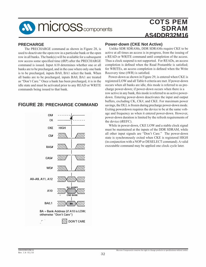
PRECHARGE The PRECHARGE command as shown in Figure 28, is used to deactivate the open row in a particular bank or the open row in all banks. The bank(s) will be available for a subsequent row access some specifi ed time (tRP) after the PRECHARGE command is issued. Input A10 determines whether one or all banks are to be precharged, and in the case where only one bank is to be precharged, inputs BA0, BA1 select the bank. When all banks are to be precharged, inputs BA0, BA1 are treated as “Don’t Care.” Once a bank has been precharged, it is in the idle state and must be activated prior to any READ or WRITE commands being issued to that bank.
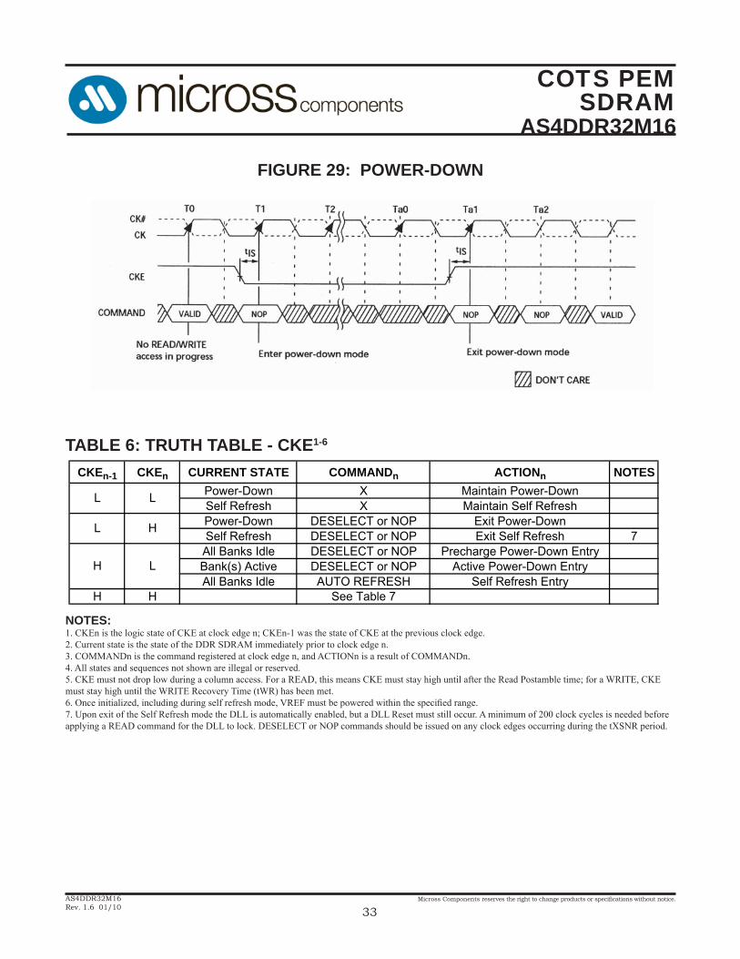
Power-down (CKE Not Active) Unlike SDR SDRAMs, DDR SDRAMs require CKE to be active at all times an access is in progress, from the issuing of a READ or WRITE command until completion of the access. Thus a clock suspend is not supported. For READs, an access completion is defi ned when the Read Postamble is satisfi ed; for WRITEs, an access completion is defi ned when the Write Recovery time (tWR) is satisfi ed. Power-down as shown in Figure 29, is entered when CKE is registered LOW and all Table 6 criteria are met. If power-down occurs when all banks are idle, this mode is referred to as pre-charge power-down; if power-down occurs when there is arow active in any bank, this mode is referred to as active power-down. Entering power-down deactivates the input and output buffers, excluding CK, CK#, and CKE. For maximum power savings, the DLL is frozen during precharge power-down mode. Exiting powerdown requires the device to be at the same volt-age and frequency as when it entered power-down. However, power-down duration is limited by the refresh requirements of the device (tREFC). While in power-down, CKE LOW and a stable clock signal must be maintained at the inputs of the DDR SDRAM, while all other input signals are “Don’t Care.” The power-down state is synchronously exited when CKE is registered HIGH (in conjunction with a NOP or DESELECT command). A valid executable command may be applied one clock cycle later.
FIGURE 28: PRECHARGE COMMAND
COTS PEMSDRAM
AS4DDR32M16
Micross Components reserves the right to change products or specifi cations without notice.
33AS4DDR32M16Rev. 1.6 01/10
FIGURE 29: POWER-DOWN
TABLE 6: TRUTH TABLE - CKE1-6
CKEn-1 CKEn CURRENT STATE COMMANDn ACTIONn NOTESPower-Down X Maintain Power-DownSelf Refresh X Maintain Self RefreshPower-Down DESELECT or NOP Exit Power-DownSelf Refresh DESELECT or NOP Exit Self Refresh 7All Banks Idle DESELECT or NOP Precharge Power-Down EntryBank(s) Active DESELECT or NOP Active Power-Down EntryAll Banks Idle AUTO REFRESH Self Refresh Entry
H H See Table 7
L
L
H
L
H
L
NOTES:1. CKEn is the logic state of CKE at clock edge n; CKEn-1 was the state of CKE at the previous clock edge.2. Current state is the state of the DDR SDRAM immediately prior to clock edge n.3. COMMANDn is the command registered at clock edge n, and ACTIONn is a result of COMMANDn.4. All states and sequences not shown are illegal or reserved.5. CKE must not drop low during a column access. For a READ, this means CKE must stay high until after the Read Postamble time; for a WRITE, CKE must stay high until the WRITE Recovery Time (tWR) has been met.6. Once initialized, including during self refresh mode, VREF must be powered within the specifi ed range.7. Upon exit of the Self Refresh mode the DLL is automatically enabled, but a DLL Reset must still occur. A minimum of 200 clock cycles is needed before applying a READ command for the DLL to lock. DESELECT or NOP commands should be issued on any clock edges occurring during the tXSNR period.

COTS PEMSDRAM
AS4DDR32M16
Micross Components reserves the right to change products or specifi cations without notice.
34AS4DDR32M16Rev. 1.6 01/10
TABLE 7: TRUTH TABLE - CURRENT STATE BANK n - COMMAND TO BANK n 1-6
CURRENTSTATE CS# RAS# CAS# WE# COMMAND/ACTION NOTES
Any H X X X DESELECT (NOP/continue previous operation)L H H H NO OPERATION (NOP/continue previous operation)L L H H ACTIVE (select and activate row)L L L H AUTO REFRESH 7L L L L LOAD MODE REGISTER 7L H L H READ (select column and start READ burst) 10L H L L WRITE (select column and start WRITE burst) 10L L H L PRECHARGE (deactivate row in bank or banks) 8L H L H READ (select column and start new READ burst) 10L H L L WRITE (select column and start WRITE burst) 10, 12L L H L PRECHARGE (truncate READ burst, start PRECHARGE) 8L H H L BURST TERMINATE 9L H L H READ (select column and start READ burst) 10, 11L H L L WRITE (select column and start new WRITE burst) 10L L H L PRECHARGE (truncate WRITE burst, start PRECHARGE) 8, 11
Write(Auto-Precharge
Idle
Row Active
Read(Auto-PrechargeDisabled)
NOTES:1. This table applies when CKEn-1 was HIGH and CKEn is HIGH (see Table 7 on page 41) and after tXSNR has been met (if the previous state was self refresh).2. This table is bank-specifi c, except where noted (i.e., the current state is for a specifi c bank and the commands shown are those allowed to be issued to that bank when in that state). Exceptions are covered in the notes below.3. Current state defi nitions: Idle:The bank has been precharged, and tRP has been met. Row Active: A row in the bank has been activated, and tRCD has been met. No data bursts/accesses and no register accesses are in progress. Read: A READ burst has been initiated, with auto precharge disabled, and has not yet terminated or been terminated. Write: A WRITE burst has been initiated, with auto precharge disabled, and has not yet terminated or been terminated.4. The following states must not be interrupted by a command issued to the same bank. COMMAND INHIBIT or NOP commands, or allowable commands to the other bank should be issued on any clock edge occurring during these states. Allowable commands to the other bank are determined by its current state and Table 7, Truth Table – Current State Bank n - Command to Bank n and according to Table 8, Truth Table – Current State Bank n - Command to Bank m. Precharging: Starts with registration of a PRECHARGE command and ends when tRP is met. Once tRP is met, the bank will be in the idle state. Row Activating: Starts with registration of an ACTIVE command and ends when tRCD is met. Once tRCD is met, the bank will be in the “row active” state. Read w/Auto-Precharge Enabled: Starts with registration of a READ command with auto precharge enabled and ends when tRP has been met. Once tRP is met, the bank will be in the idle state. Write w/Auto-Precharge Enabled: Starts with registration of a WRITE command with auto precharge enabled and ends when tRP has been met. Once tRP is met, the bank will be in the idle state.5. The following states must not be interrupted by any executable command; COMMAND INHIBIT or NOP commands must be applied on each positive clock edge during these states. Refreshing: Starts with registration of an AUTO REFRESH command and ends when tRFC is met. Once tRFC is met, the DDR SDRAM will be in the all banks idle state. Accessing Mode Register: Starts with registration of a LOAD MODE REGISTER command and ends when tMRD has been met. Once tMRD is met, the DDR SDRAM will be in the all banks idle state. Precharging All: Starts with registration of a PRECHARGE ALL command and ends when tRP is met. Once tRP is met, all banks will be in the idle state.6. All states and sequences not shown are illegal or reserved.7. Not bank-specifi c; requires that all banks are idle, and bursts are not in progress.8. May or may not be bank-specifi c; if multiple banks are to be precharged, each must be in a valid state for precharging.9. Not bank-specifi c; BURST TERMINATE affects the most recent READ burst, regardless of bank.10. READs or WRITEs listed in the Command/Action column include Reads or Writes with auto precharge enabled and READs or WRITEs with auto pre-charge disabled.11. Requires appropriate DM masking.12. A WRITE command may be applied after the completion of the READ burst; otherwise, a BURST TERMINATE must be used to end the READ burst prior to asserting a WRITE command.

COTS PEMSDRAM
AS4DDR32M16
Micross Components reserves the right to change products or specifi cations without notice.
35AS4DDR32M16Rev. 1.6 01/10
TABLE 8: TRUTH TABLE - CURRENT STATE BANK n - COMMAND TO BANK m 1-6
CURRENTSTATE CS# RAS# CAS# WE# COMMAND/ACTION NOTES
H X X X DESELECT (NOP/continue previous operation)L H H H NO OPERATION (NOP/continue previous operation)
Idle X X X X Any Command Otherwise Allowed to Bank mL L H H ACTIVE (select and activate row)L H L H READ (select column and start READ burst) 7L H L L WRITE (select column and start WRITE burst) 7L L H L PRECHARGEL L H H ACTIVE (select and activate row)L H L H READ (select column and start new READ burst) 7L H L L WRITE (select column and start WRITE burst) 7, 9L L H L PRECHARGEL L H H ACTIVE (select and activate row)L H L H READ (select column and start READ burst) 7, 8L H L L WRITE (select column and start new WRITE burst) 7L L H L PRECHARGEL L H H ACTIVE (select and activate row)L H L H READ (select column and start new READ burst) 7, 3aL H L L WRITE (select column and start WRITE burst) 7, 9, 3aL L H L PRECHARGEL L H H ACTIVE (select and activate row)L H L H READ (select column and start READ burst) 7, 3aL H L L WRITE (select column and start new WRITE burst) 7, 3aL L H L PRECHARGE
Write(With Auto-Precharge)
Any
RowActivating,Active, or Precharging
Read(Auto-
PrechargeDisabled)
Write(Auto-PrechargeDisabled)
Read(With Auto-Precharge)
NOTES:1. This table applies when CKEn-1 was HIGH and CKEn is HIGH (see Truth Table 2) and after tXSNR has been met (if the previous state was self refresh).2. This table describes alternate bank operation, except where noted (i.e., the current state is for bank n and the commands shown are those allowed to be issued to bank m, assuming that bank m is in such a state that the given command is allowable). Exceptions are covered in the notes below.3. Current state defi nitions: Idle: The bank has been precharged, and tRP has been met. Row Active: A row in the bank has been activated, and tRCD has been met. No data bursts/accesses and no register accesses are in progress. Read: A READ burst has been initiated, with auto precharge disabled, and has not yet terminated or been terminated. Write:A WRITE burst has been initiated, with auto precharge disabled, and has not yet terminated or been terminated Read with Auto Precharge Enabled: See following text – 3a Write with Auto Precharge Enabled: See following text – 3a
a. The read with auto precharge enabled or write with auto precharge enabled states can each be broken into two parts: the access period and the pre-charge period. For read with auto precharge, the precharge period is defi ned as if the same burst was executed with auto precharge disabled and then followed with the earliest possible PRECHARGE command that still accesses all of the data in the burst. For write with auto precharge, the precharge period begins when tWR ends, with tWR measured as if auto precharge was disabled. The access period starts with registration of the command and ends where the precharge period (or tRP) begins.This device supports concurrent auto precharge such that when a read with auto precharge is enabled or a write with auto precharge is enabled any command to other banks is allowed, as long as that command does not interrupt the read or write data transfer already in process. In either case, all other related limitations apply (e.g., contention between read data and write data must be avoided).b. The minimum delay from a read or write command with auto precharge enabled, to a command to a different bank is summarized on the following page.
(CONTINUED)
COTS PEMSDRAM
AS4DDR32M16
Micross Components reserves the right to change products or specifi cations without notice.
36AS4DDR32M16Rev. 1.6 01/10
NOTES (Continued):
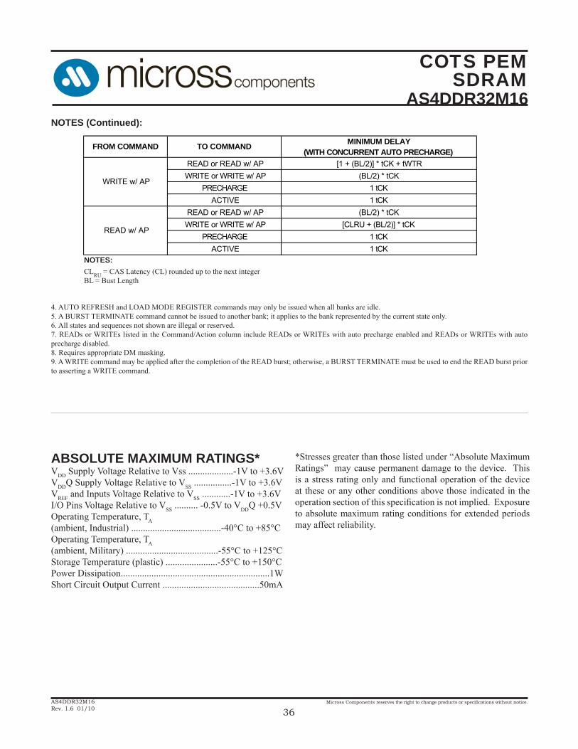
FROM COMMAND TO COMMAND MINIMUM DELAY(WITH CONCURRENT AUTO PRECHARGE)
READ or READ w/ AP [1 + (BL/2)] * tCK + tWTRWRITE or WRITE w/ AP (BL/2) * tCK
PRECHARGE 1 tCKACTIVE 1 tCK
READ or READ w/ AP (BL/2) * tCKWRITE or WRITE w/ AP [CLRU + (BL/2)] * tCK
PRECHARGE 1 tCKACTIVE 1 tCK
WRITE w/ AP
READ w/ AP
NOTES:CLRU = CAS Latency (CL) rounded up to the next integerBL = Bust Length
4. AUTO REFRESH and LOAD MODE REGISTER commands may only be issued when all banks are idle.5. A BURST TERMINATE command cannot be issued to another bank; it applies to the bank represented by the current state only.6. All states and sequences not shown are illegal or reserved.7. READs or WRITEs listed in the Command/Action column include READs or WRITEs with auto precharge enabled and READs or WRITEs with auto precharge disabled.8. Requires appropriate DM masking.9. A WRITE command may be applied after the completion of the READ burst; otherwise, a BURST TERMINATE must be used to end the READ burst prior to asserting a WRITE command.
*Stresses greater than those listed under “Absolute Maximum Ratings” may cause permanent damage to the device. This is a stress rating only and functional operation of the device at these or any other conditions above those indicated in the operation section of this specifi cation is not implied. Exposure to absolute maximum rating conditions for extended periods may affect reliability.
ABSOLUTE MAXIMUM RATINGS*VDD Supply Voltage Relative to Vss ...................-1V to +3.6VVDDQ Supply Voltage Relative to VSS ................-1V to +3.6VVREF and Inputs Voltage Relative to VSS ............-1V to +3.6VI/O Pins Voltage Relative to VSS .......... -0.5V to VDDQ +0.5VOperating Temperature, TA(ambient, Industrial) ......................................-40°C to +85°COperating Temperature, TA(ambient, Military) .......................................-55°C to +125°CStorage Temperature (plastic) ......................-55°C to +150°CPower Dissipation...............................................................1WShort Circuit Output Current .........................................50mA
COTS PEMSDRAM
AS4DDR32M16
Micross Components reserves the right to change products or specifi cations without notice.
37AS4DDR32M16Rev. 1.6 01/10
TABLE 9: DC ELECTRICAL CHARACTERISTICS AND OPERATION CONDITIONS (-55°C < TA < +125°C; VDDQ = +2.5V ±0.2V, VDD = +2.5V ±0.2V) 1-5, 14, 16
PARAMETER SYM MIN MAX UNITS NOTES
Supply Voltage VDD 2.3 2.7 V 36, 41
I/O Supply Voltage VDDQ 2.3 2.7 V 36, 41, 44
I/O Reference Voltage VREF 0.49 x VDDQ 0.51 x VDDQ V 6, 44
I/O Termination Voltage (system) VTT VREF - 0.04 VREF + 0.04 V 7, 44
Input High (Logic 1) Voltage VIH(DC) VREF + 0.15 VDD + 0.3 V 28
Input Low (Logic 0) Voltage VIL(DC) -0.3 VREF - 0.15 V 28
INPUT LEAKAGE CURRENTAny input 0V < VIN < VDD, VREF PIN 0V < VIN < 1.35V(All other pins not under test - 0V)
II -2 2 μA
OUTPUT LEAKAGE CURRENT(DQs are disabled; 0V < VOUT < VDDQ) IOZ -5 5 μA
IOH -16.8 --- mA
IOL 16.8 --- mA
IOHR -9 --- mA
IOLR 9 --- mA
OUTPUT LEVELS: Full drive optionHigh Current (VOUT = VDDQ - 0.373V, min. VREF, min. VTT
Low Current (VOUT = 0.373V, max. VREF, max. VTT)
OUTPUT LEVELS: Reduced drive optionHigh Current (VOUT = VDDQ - 0.763V, min. VREF, min. VTT
Low Current (VOUT = 0.763V, max. VREF, max. VTT)
37, 39
38, 39
TABLE 10: AC INPUT OPERATING CONDITIONS (-55°C < TA < +125°C; VDDQ = +2.5V ±0.2V, VDD = +2.5V ±0.2V) 1-5, 14, 16
PARAMETER SYM MIN MAX UNITS NOTESInput High (Logic 1) Voltage VIH(AC) VREF + 0.310 --- V 14, 28, 40
Input Low (Logic 0) Voltage VIL(AC) --- VREF - 0.310 V 14, 28, 40
I/O Reference Voltage VREF(AC) 0.49 x VDDQ 0.51 x VDDQ V 6
COTS PEMSDRAM
AS4DDR32M16
Micross Components reserves the right to change products or specifi cations without notice.
38AS4DDR32M16Rev. 1.6 01/10
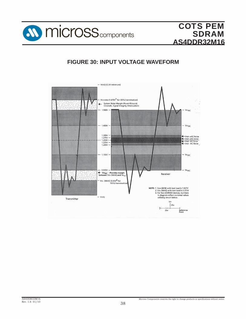
FIGURE 30: INPUT VOLTAGE WAVEFORM
COTS PEMSDRAM
AS4DDR32M16
Micross Components reserves the right to change products or specifi cations without notice.
39AS4DDR32M16Rev. 1.6 01/10
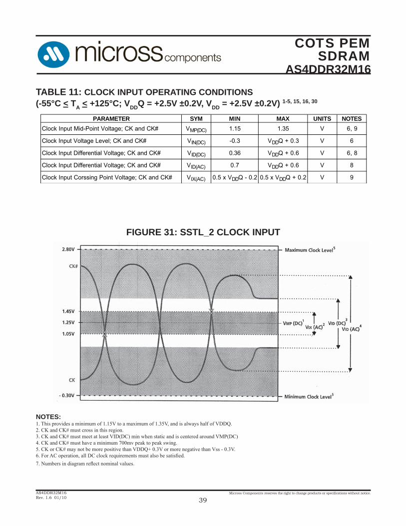
TABLE 11: CLOCK INPUT OPERATING CONDITIONS (-55°C < TA < +125°C; VDDQ = +2.5V ±0.2V, VDD = +2.5V ±0.2V) 1-5, 15, 16, 30
PARAMETER SYM MIN MAX UNITS NOTESClock Input Mid-Point Voltage; CK and CK# VMP(DC) 1.15 1.35 V 6, 9
Clock Input Voltage Level; CK and CK# VIN(DC) -0.3 VDDQ + 0.3 V 6
Clock Input Differential Voltage; CK and CK# VID(DC) 0.36 VDDQ + 0.6 V 6, 8
Clock Input Differential Voltage; CK and CK# VID(AC) 0.7 VDDQ + 0.6 V 8
Clock Input Corssing Point Voltage; CK and CK# VIX(AC) 0.5 x VDDQ - 0.2 0.5 x VDDQ + 0.2 V 9
FIGURE 31: SSTL_2 CLOCK INPUT
NOTES:1. This provides a minimum of 1.15V to a maximum of 1.35V, and is always half of VDDQ.2. CK and CK# must cross in this region.3. CK and CK# must meet at least VID(DC) min when static and is centered around VMP(DC)4. CK and CK# must have a minimum 700mv peak to peak swing.5. CK or CK# may not be more positive than VDDQ+ 0.3V or more negative than Vss - 0.3V.6. For AC operation, all DC clock requirements must also be satisfi ed.7. Numbers in diagram refl ect nominal values.
COTS PEMSDRAM
AS4DDR32M16
Micross Components reserves the right to change products or specifi cations without notice.
40AS4DDR32M16Rev. 1.6 01/10
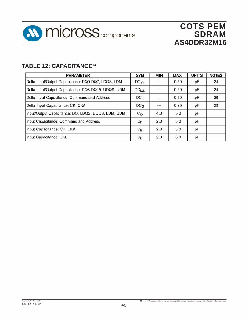
TABLE 12: CAPACITANCE13
PARAMETER SYM MIN MAX UNITS NOTESDelta Input/Output Capacitance: DQ0-DQ7, LDQS, LDM DCIOL --- 0.50 pF 24
Delta Input/Output Capacitance: DQ8-DQ15, UDQS, UDM DCIOU --- 0.50 pF 24
Delta Input Capacitance: Command and Address DCI1 --- 0.50 pF 29
Delta Input Capacitance: CK, CK# DCI2 --- 0.25 pF 29
Input/Output Capacitance: DQ, LDQS, UDQS, LDM, UDM CIO 4.0 5.0 pF
Input Capacitance: Command and Address CI1 2.0 3.0 pF
Input Capacitance: CK, CK# CI2 2.0 3.0 pF
Input Capacitance: CKE CI3 2.0 3.0 pF
COTS PEMSDRAM
AS4DDR32M16
Micross Components reserves the right to change products or specifi cations without notice.
41AS4DDR32M16Rev. 1.6 01/10
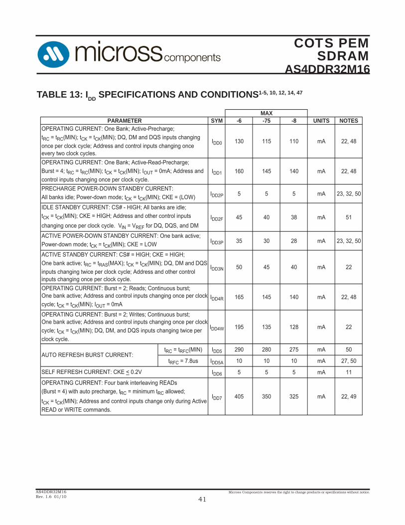
TABLE 13: IDD SPECIFICATIONS AND CONDITIONS1-5, 10, 12, 14, 47
MAXPARAMETER SYM -6 -75 -8 UNITS NOTES
OPERATING CURRENT: One Bank; Active-Precharge;tRC = tRC(MIN); tCK = tCK(MIN); DQ, DM and DQS inputs changing once per clock cycle; Address and control inputs changing once every two clock cycles.
IDD0 130 115 110 mA 22, 48
OPERATING CURRENT: One Bank; Active-Read-Precharge;Burst = 4; tRC = tRC(MIN); tCK = tCK(MIN); IOUT = 0mA; Address and control inputs changing once per clock cycle.
IDD1 160 145 140 mA 22, 48
PRECHARGE POWER-DOWN STANDBY CURRENT:All banks idle; Power-down mode; tCK = tCK(MIN); CKE = (LOW) IDD2P 5 5 5 mA 23, 32, 50
IDLE STANDBY CURRENT: CS# - HIGH; All banks are idle;tCK = tCK(MIN); CKE = HIGH; Address and other control inputs changing once per clock cycle. VIN = VREF for DQ, DQS, and DM
IDD2F 45 40 38 mA 51
ACTIVE POWER-DOWN STANDBY CURRENT: One bank active; Power-down mode; tCK = tCK(MIN); CKE = LOW IDD3P 35 30 28 mA 23, 32, 50
ACTIVE STANDBY CURRENT: CS# = HIGH; CKE = HIGH;One bank active; tRC = tRAS(MAX); tCK = tCK(MIN); DQ, DM and DQS inputs changing twice per clock cycle; Address and other control inputs changing once per clock cycle.
IDD3N 50 45 40 mA 22
OPERATING CURRENT: Burst = 2; Reads; Continuous burst;One bank active; Address and control inputs changing once per clockcycle; tCK = tCK(MIN); IOUT = 0mA
IDD4R 165 145 140 mA 22, 48
OPERATING CURRENT: Burst = 2; Writes; Continuous burst;One bank active; Address and control inputs changing once per clockcycle; tCK = tCK(MIN); DQ, DM, and DQS inputs changing twice per clock cycle.
IDD4W 195 135 128 mA 22
AUTO REFRESH BURST CURRENT:tRC = tRFC(MIN) IDD5 290 280 275 mA 50
tRFC = 7.8us IDD5A 10 10 10 mA 27, 50
SELF REFRESH CURRENT: CKE < 0.2V IDD6 5 5 5 mA 11
OPERATING CURRENT: Four bank interleaving READs(Burst = 4) with auto precharge, tRC = minimum tRC allowed;tCK = tCK(MIN); Address and control inputs change only during Active READ or WRITE commands.
IDD7 405 350 325 mA 22, 49

COTS PEMSDRAM
AS4DDR32M16
Micross Components reserves the right to change products or specifi cations without notice.
42AS4DDR32M16Rev. 1.6 01/10
TABLE 14: IDD TEST CYCLE TIMES (Values refl ect number of clock cycles for each test.)
IDD TEST SPEEDGRADE
CLOCKCYCLETIME
tRRD tRCD tRAS tRP tRC tRFC tREFI CL
IDD0-6 6ns N/A N/A 7 3 10 N/A N/A N/A-75 7.5ns N/A N/A 6 3 9 N/A N/A N/A-8 8ns N/A N/A N/A N/A N/A
IDD1-6 6ns N/A N/A 7 3 10 N/A N/A 2.5-75 7.5ns N/A N/A 6 3 9 N/A N/A 2.5-8 8ns N/A N/A N/A N/A
IDD4R-6 6ns N/A N/A N/A N/A N/A N/A N/A 2.5-75 7.5ns N/A N/A N/A N/A N/A N/A N/A 2.5-8 8ns N/A N/A N/A N/A N/A N/A N/A
IDD4W-6 6ns N/A N/A N/A N/A N/A N/A N/A N/A-75 7.5ns N/A N/A N/A N/A N/A N/A N/A N/A-8 8ns N/A N/A N/A N/A N/A N/A N/A N/A
IDD5-6 6ns N/A N/A N/A N/A N/A 12 12 N/A-75 7.5ns N/A N/A N/A N/A N/A 10 10 N/A-8 8ns N/A N/A N/A N/A N/A N/A
IDD5A-6 6ns N/A N/A N/A N/A N/A 12 1288 N/A-75 7.5ns N/A N/A N/A N/A N/A 10 1029 N/A-8 8ns N/A N/A N/A N/A N/A N/A
IDD7-6 6ns 2/4 3 N/A 3 10 N/A N/A 2.5-75 7.5ns 2/4 3 N/A 3 10 N/A N/A 2.5-8 8ns N/A N/A N/A
COTS PEMSDRAM
AS4DDR32M16
Micross Components reserves the right to change products or specifi cations without notice.
43AS4DDR32M16Rev. 1.6 01/10
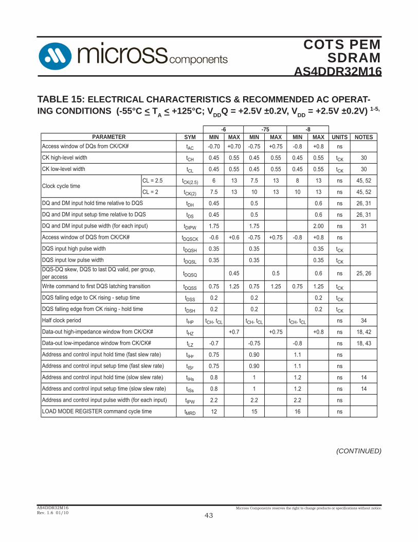
TABLE 15: ELECTRICAL CHARACTERISTICS & RECOMMENDED AC OPERAT-ING CONDITIONS (-55°C < TA < +125°C; VDDQ = +2.5V ±0.2V, VDD = +2.5V ±0.2V) 1-5,
-6 -75 -8PARAMETER SYM MIN MAX MIN MAX MIN MAX UNITS NOTES
Access window of DQs from CK/CK# tAC -0.70 +0.70 -0.75 +0.75 -0.8 +0.8 ns
CK high-level width tCH 0.45 0.55 0.45 0.55 0.45 0.55 tCK 30
CK low-level width tCL 0.45 0.55 0.45 0.55 0.45 0.55 tCK 30
Clock cycle timeCL = 2.5 tCK(2.5) 6 13 7.5 13 8 13 ns 45, 52
CL = 2 tCK(2) 7.5 13 10 13 10 13 ns 45, 52
DQ and DM input hold time relative to DQS tDH 0.45 0.5 0.6 ns 26, 31
DQ and DM input setup time relative to DQS tDS 0.45 0.5 0.6 ns 26, 31
DQ and DM input pulse width (for each input) tDIPW 1.75 1.75 2.00 ns 31
Access window of DQS from CK/CK# tDQSCK -0.6 +0.6 -0.75 +0.75 -0.8 +0.8 ns
DQS input high pulse width tDQSH 0.35 0.35 0.35 tCK
DQS input low pulse width tDQSL 0.35 0.35 0.35 tCKDQS-DQ skew, DQS to last DQ valid, per group,per access tDQSQ 0.45 0.5 0.6 ns 25, 26
Write command to first DQS latching transition tDQSS 0.75 1.25 0.75 1.25 0.75 1.25 tCK
DQS falling edge to CK rising - setup time tDSS 0.2 0.2 0.2 tCK
DQS falling edge from CK rising - hold time tDSH 0.2 0.2 0.2 tCK
Half clock period tHP tCH, tCL tCH, tCL tCH, tCL ns 34
Data-out high-impedance window from CK/CK# tHZ +0.7 +0.75 +0.8 ns 18, 42
Data-out low-impedance window from CK/CK# tLZ -0.7 -0.75 -0.8 ns 18, 43
Address and control input hold time (fast slew rate) tIHF 0.75 0.90 1.1 ns
Address and control input setup time (fast slew rate) tISF 0.75 0.90 1.1 ns
Address and control input hold time (slow slew rate) tIHs 0.8 1 1.2 ns 14
Address and control input setup time (slow slew rate) tISs 0.8 1 1.2 ns 14
Address and control input pulse width (for each input) tIPW 2.2 2.2 2.2 ns
LOAD MODE REGISTER command cycle time tMRD 12 15 16 ns
(CONTINUED)
COTS PEMSDRAM
AS4DDR32M16
Micross Components reserves the right to change products or specifi cations without notice.
44AS4DDR32M16Rev. 1.6 01/10
TABLE 15: ELECTRICAL CHARACTERISTICS & RECOMMENDED AC OPERAT-ING CONDITIONS (CONTINUED) 1-5, 14-17, 33
-6 -75 -8PARAMETER SYM MIN MAX MIN MAX MIN MAX UNITS NOTES
DQ-DQS hold, DQS to first DQ to go non-valid,per access tQH tHP - tQHS tHP - tQHS tHP - tQHS ns 25, 26
Data Hold Skew Factor tQHS 0.55 0.75 1.0 ns
ACTIVE to PRECHARGE command tRAS 42 70,000 40 120,000 40 120,000 ns 35
ACTIVE to READ with Auto precharge command tRAP 15 20 20 ns
ACTIVE to ACTIVE/AUTO REFRESH command period tRC 60 65 70 ns
AUTO REFRESH command period tRFC 72 75 80 ns 50
ACTIVE to READ or WRITE delay tRCD 15 20 20 ns
PRECHARGE command period tRP 15 20 20 ns
DQS read preamble tRPRE 0.9 1.1 0.9 1.1 0.9 1.1 tCK 42
DQS read postamble tRPST 0.4 0.6 0.4 0.6 0.4 0.6 tCK
ACTIVE bank a b tRRD to Active bank command 12 15 16 ns
DQS write preamble tWPRE 0.25 0.25 0.25 tCK
DQS write preamble setup time tWPRES 0 0 0 ns 20, 21
DQS write postamble tWPST 0.4 0.6 0.4 0.6 0.4 0.6 tCK 19
Write recovery time tWR 15 15 18 ns
Internal WRITE to READ command delay tWTR 1 1 1 tCK
Data valid ouput window (DVW) N/A tQH - tDQSQ tQH - tDQSQ tQH - tDQSQ ns 25REFRESH to REFRESH command interval tREFC 70.3 70.3 70.3 s 23
Average periodic refresh interval tREFI 7.8 7.8 7.8 s 23
Terminating voltage delay to V tVTDDD 0 0 0 ns
Exit SELF REFRESH to non-READ command tXSNR 75 75 80 ns
Exit SELF REFRESH to READ command tXSRD 200 200 200 tCK
TABLE 16: INPUT SLEW RATE DERATING VALUES FOR ADDRESSES AND COMMANDS FOR -75 OPTION (-55°C < TA < +125°C; VDDQ = +2.5V ±0.2V, VDD = +2.5V ±0.2V) 14
TABLE 17: INPUT SLEW RATE DERATING VALUES FOR DQ, DQS, & DM FOR -75 OPTION (-55°C < TA < +125°C; VDDQ = +2.5V ±0.2V, VDD = +2.5V ±0.2V) 31
SLEW RATE tIS tIH UNITS
0.500V/ns 1.00 1 ns0.400V/ns 1.05 1 ns0.300V/ns 1.15 1 ns
SLEW RATE tDS tDH UNITS
0.500V/ns 0.50 0.50 ns0.400V/ns 0.55 0.55 ns0.300V/ns 0.60 0.60 ns
COTS PEMSDRAM
AS4DDR32M16
Micross Components reserves the right to change products or specifi cations without notice.
45AS4DDR32M16Rev. 1.6 01/10
NOTES:1. All voltages referenced to VSS.2. Tests for AC timing, IDD, and electrical AC and DC characteristics may be conducted at nominal reference/supply voltage levels, but the related specifi cations and device operation are guaranteed for the full voltage range specifi ed.3. Outputs (except for IDD measurements) measured with equivalent load:
4. AC timing and IDD tests may use a VIL-to-VIH swing of up to 1.5V in the test environment, but input timing is still referenced to VREF (or to the cross-ing point for CK/CK#), and parameter specifi cations are guaranteed for the specifi ed AC input levels under normal use conditions. The minimum slew rate for the input signals used to test the device is 1V/ns in the range between VIL(AC) and VIH(AC).5. The AC and DC input level specifi cations are as defi ned in the SSTL_2 Standard (i.e., the receiver will effectively switch as a result of the signalcrossing the AC input level, and will remain in that state as long as the signal does not ring back above [below] the DC input LOW [HIGH] level).6. VREF is expected to equal VDDQ/2 of the transmitting device and to track variations in the DC level of the same. Peak-to-peak noise (non-common mode) on VREF may not exceed ±2 percent of the DC value. Thus, from VDDQ/2, VREF is allowed ±25mV for DC error and an additional ±25mV for AC noise. This measurement is to be taken at the nearest VREF by-pass capacitor.7. VTT is not applied directly to the device. VTT is a system supply for signal termination resistors, is expected to be set equal to VREF and must track varia-tions in the DC level of VREF.8. VID is the magnitude of the difference between the input level on CK and the input level on CK#.9. The value of VIX and VMP are expected to equal VDDQ/2 of the trans-mitting device and must track variations in the DC level of the same.10. IDD is dependent on output loading and cycle rates. Specifi ed values are obtained with minimum cycle times at CL=2.5 with the outputs open.11. Enables on-chip refresh and address counters.12. IDD specifi cations are tested after the device is properly initialized, and is averaged at the defi ned cycle rate.13. This parameter is sampled. VDD=+2.5V±0.2V, VDDQ=+2.5V±0.2V, VREF=VSS, f=100MHz, TA=25°C VOUT(DC)=VDDQ/2, VOUT (peak to peak)=0.2V. DM input is grouped with I/O pins, refl ecting the fact that they are matched in loading.14. For slew rates less than 1V/ns and and greater than or equal to 0.5V/ns. If the slew rate is less than 0.5V/ns, timing must be derated: tIS has anadditional 50ps per each 100mV/ns reduction in slew rate from the 500mV/ns. tIH has 0ps added, that is, it remains constant. If the slew rate exceeds 4.5V/ns, functionality is uncertain.15. The CK/CK# input reference level (for timing referenced to CK/CK#) is the point at which CK and CK# cross; the input reference level for signals other than CK/CK# is VREF.16. Inputs are not recognized as valid until VREF stabilizes. Once initial-ized, including self refresh mode, VREF must be powered within specifi ed range. Exception: during the period before VREF stabilizes, CKE 0.3 x VDDQ is recognized as LOW.17. The output timing reference level, as measured at the timing reference point indicated in Note 3, is VTT.
18. tHZ and tLZ transitions occur in the same access time windows as data valid transitions. These parameters are not referenced to a specifi c voltage level, but specify when the device output is no longer driving (HZ) or begins driving (LZ).19. The intent of the Don’t Care state after completion of the postamble is the DQS-driven signal should either be high, low, or high-Z and that any signal transition within the input switching region must follow valid input require-ments. That is, if DQS transitions high (above VIHDC(MIN) then it must not transition low (below VIHDC) prior to tDQSH(MIN).20. This is not a device limit. The device will operate with a negative value, but system performance could be degraded due to bus turnaround.21. It is recommended that DQS be valid (HIGH or LOW) on or before the WRITE command. The case shown (DQS going from High-Z to logicLOW) applies when no WRITEs were previously in progress on the bus. If a previous WRITE was in progress, DQS could be HIGH during this time, depending on tDQSS.22. MIN (tRC or tRFC) for IDD measurements is the smallest multiple of tCK that meets the minimum absolute value for the respective parameter. tRAS (MAX) for IDD measurements is the largest multiple of tCK that meets the maximum absolute value for tRAS.23. The refresh period is 64ms. This equates to an average refresh rate of 7.8125μs. However, an AUTO REFRESH command must be asserted at least once every 70.3μs; burst refreshing or posting by the DRAM control-ler greater than eight refresh cycles is not allowed.24. The I/O capacitance per DQS and DQ byte/group will not differ by more than this maximum amount for any given device.25. The data valid window is derived by achieving other specifi cations - tHP (tCK/2), tDQSQ, and tQH (tQH = tHP - tQHS). The data valid window derates in direct proportion to the clock duty cycle and a practical data valid window can be derived. The clock is allowed a maximum duty cycle variation of 45/55, because functionality is uncertain when operating beyond a 45/55 ratio. The data valid window derating curves are provided in Figure 32 for duty cycles ranging between 50/50 and 45/55.26. Referenced to each output group: x4 = DQS with DQ0-DQ3; x8 = DQS with DQ0-DQ7; x16 = LDQS with DQ0-DQ7; and UDQS with DQ8-DQ15.27. This limit is actually a nominal value and does not result in a fail value. CKE is HIGH during REFRESH command period (tRFC [MIN]) else CKE is LOW (i.e., during standby).28. To maintain a valid level, the transitioning edge of the input must: a. Sustain a constant slew rate from the current AC level through to the target AC level, VIL(AC) or VIH(AC). b. Reach at least the target AC level. c. After the AC target level is reached, continue to maintain at least the target DC level, VIL(DC) or VIH(DC).29. The Input capacitance per pin group will not differ by more than this maximum amount for any given device.30. CK and CK# input slew rate must be > 1V/ns (> 2V/ns if measured dif-ferentially).31. DQ and DM input slew rates must not deviate from DQS by more than 10 percent. If the DQ/DM/DQS slew rate is less than 0.5V/ns, timing must be derated: 50ps must be added to tDS and tDH for each 100mv/ns reduction in slew rate. For -6 speed grades, slew rate must be > 0.5V/ns. If slew rate exceeds 4V/ns, functionality is uncertain.32. VDD must not vary more than 4 percent if CKE is not active while any bank is active.33. The clock is allowed up to ±150ps of jitter. Each timing parameter is al-lowed to vary by the same amount.34. tHP (MIN) is the lesser of tCL minimum and tCH minimum actually applied to the device CK and CK# inputs, collectively during bank active.
(continued)
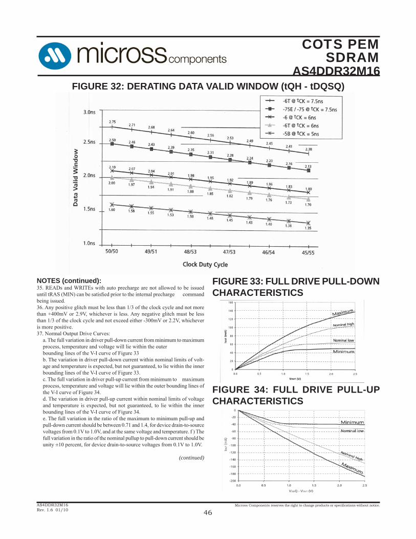
COTS PEMSDRAM
AS4DDR32M16
Micross Components reserves the right to change products or specifi cations without notice.
46AS4DDR32M16Rev. 1.6 01/10
NOTES (continued):35. READs and WRITEs with auto precharge are not allowed to be issued until tRAS (MIN) can be satisfi ed prior to the internal precharge command being issued.36. Any positive glitch must be less than 1/3 of the clock cycle and not more than +400mV or 2.9V, whichever is less. Any negative glitch must be less than 1/3 of the clock cycle and not exceed either -300mV or 2.2V, whichever is more positive.37. Normal Output Drive Curves:
a. The full variation in driver pull-down current from minimum to maximum process, temperature and voltage will lie within the outerbounding lines of the V-I curve of Figure 33b. The variation in driver pull-down current within nominal limits of volt-age and temperature is expected, but not guaranteed, to lie within the inner bounding lines of the V-I curve of Figure 33.c. The full variation in driver pull-up current from minimum to maximum process, temperature and voltage will lie within the outer bounding lines of the V-I curve of Figure 34.d. The variation in driver pull-up current within nominal limits of voltage and temperature is expected, but not guaranteed, to lie within the inner bounding lines of the V-I curve of Figure 34.e. The full variation in the ratio of the maximum to minimum pull-up and pull-down current should be between 0.71 and 1.4, for device drain-to-source voltages from 0.1V to 1.0V, and at the same voltage and temperature. f ) The full variation in the ratio of the nominal pullup to pull-down current should be unity ±10 percent, for device drain-to-source voltages from 0.1V to 1.0V.
(continued)
FIGURE 32: DERATING DATA VALID WINDOW (tQH - tDQSQ)
FIGURE 33: FULL DRIVE PULL-DOWN CHARACTERISTICS
FIGURE 34: FULL DRIVE PULL-UP CHARACTERISTICS
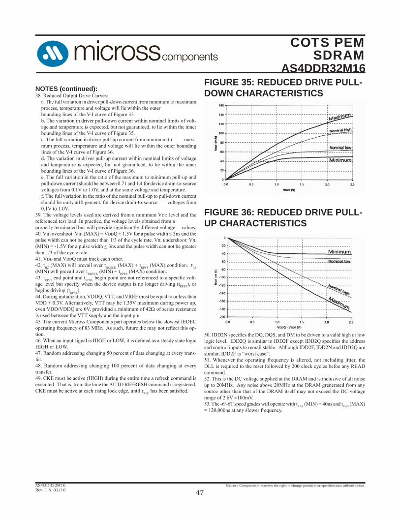
COTS PEMSDRAM
AS4DDR32M16
Micross Components reserves the right to change products or specifi cations without notice.
47AS4DDR32M16Rev. 1.6 01/10
NOTES (continued):38. Reduced Output Drive Curves:
a. The full variation in driver pull-down current from minimum to maximum process, temperature and voltage will lie within the outerbounding lines of the V-I curve of Figure 35.b. The variation in driver pull-down current within nominal limits of volt-age and temperature is expected, but not guaranteed, to lie within the inner bounding lines of the V-I curve of Figure 35.c. The full variation in driver pull-up current from minimum to maxi-mum process, temperature and voltage will lie within the outer bounding lines of the V-I curve of Figure 36.d. The variation in driver pull-up current within nominal limits of voltage and temperature is expected, but not guaranteed, to lie within the inner bounding lines of the V-I curve of Figure 36.e. The full variation in the ratio of the maximum to minimum pull-up and pull-down current should be between 0.71 and 1.4 for device drain-to-source voltages from 0.1V to 1.0V, and at the same voltage and temperature.f. The full variation in the ratio of the nominal pull-up to pull-down current should be unity ±10 percent, for device drain-to-source voltages from 0.1V to 1.0V.
39. The voltage levels used are derived from a minimum VDD level and the referenced test load. In practice, the voltage levels obtained from aproperly terminated bus will provide signifi cantly different voltage values.40. VIH overshoot: VIH (MAX) = VDDQ + 1.5V for a pulse width < 3ns and the pulse width can not be greater than 1/3 of the cycle rate. VIL undershoot: VIL (MIN) = -1.5V for a pulse width < 3ns and the pulse width can not be greater than 1/3 of the cycle rate.41. VDD and VDDQ must track each other.42. tHZ (MAX) will prevail over tDQSCK (MAX) + tRPST (MAX) condition. tLZ (MIN) will prevail over tDQSCK (MIN) + tRPRE (MAX) condition. 43. tRPST end point and tRPRE begin point are not referenced to a specifi c volt-age level but specify when the device output is no longer driving (tRPST), or begins driving (tRPRE).44. During initialization, VDDQ, VTT, and VREF must be equal to or less than VDD + 0.3V. Alternatively, VTT may be 1.35V maximum during power up, even VDD/VDDQ are 0V, providind a minimum of 42Ω of series resistance is used between the VTT supply and the input pin.45. The current Micross Components part operates below the slowest JEDEC operating frequency of 83 MHz. As such, future die may not refl ect this op-tion.46. When an input signal is HIGH or LOW, it is defi ned as a steady state logic HIGH or LOW.47. Random addressing changing 50 percent of data changing at every trans-fer.48. Random addressing changing 100 percent of data changing at every transfer.49. CKE must be active (HIGH) during the entire time a refresh command is executed. That is, from the time the AUTO REFRESH command is registered, CKE must be active at each rising lock edge, until rRFC has been satisfi ed.
FIGURE 35: REDUCED DRIVE PULL-DOWN CHARACTERISTICS
FIGURE 36: REDUCED DRIVE PULL-UP CHARACTERISTICS
50. IDD2N specifi es the DQ, DQS, and DM to be driven to a valid high or low logic level. IDD2Q is similar to IDD2F except IDD2Q specifi es the address and control inputs to remail stable. Although IDD2F, IDD2N and IDD2Q are similar, IDD2F is “worst case”.51. Whenever the operating frequency is altered, not including jitter, the DLL is required to the reset followed by 200 clock cycles befoe any READ command.52. This is the DC voltage supplied at the DRAM and is inclusive of all noise up to 20MHz. Any noise above 20MHz at the DRAM grenerated from any source other than that of the DRAM itself may not exceed the DC voltage range of 2.6V ±100mV.53. The -6/-6T speed grades will operate with tRAS (MIN) = 40ns and tRAS (MAX) = 120,000ns at any slower frequency.
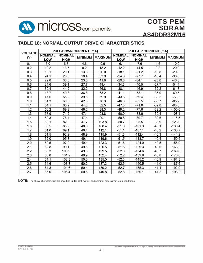
COTS PEMSDRAM
AS4DDR32M16
Micross Components reserves the right to change products or specifi cations without notice.
48AS4DDR32M16Rev. 1.6 01/10
TABLE 18: NORMAL OUTPUT DRIVE CHARACTERISTICS
NOMINALLOW
NOMINALHIGH MINIMUM MAXIMUM NOMINAL
LOWNOMINAL
HIGH MINIMUM MAXIMUM
0.1 6.0 6.8 4.6 9.6 -6.1 -7.6 -4.6 -10.00.2 12.2 13.5 9.2 18.2 -12.2 -14.5 -9.2 -20.00.3 18.1 20.1 13.8 26.0 -18.1 -21.2 -13.8 -29.80.4 24.1 26.6 18.4 33.9 -24.0 -27.7 -18.4 -38.80.5 29.8 33.0 23.0 41.8 -29.8 -34.1 -23.0 -46.80.6 34.6 39.1 27.7 49.4 -34.3 -40.5 -27.7 -54.40.7 39.4 44.2 32.2 56.8 -38.1 -46.9 -32.2 -61.80.8 43.7 49.8 36.8 63.2 -41.1 -53.1 -36.0 -69.50.9 47.5 55.2 39.6 69.9 -43.8 -59.4 -38.2 -77.31.0 51.3 60.3 42.6 76.3 -46.0 -65.5 -38.7 -85.21.1 54.1 65.2 44.8 82.5 -47.8 -71.6 -39.0 -93.01.2 56.2 69.9 46.2 88.3 -49.2 -77.6 -39.2 -100.61.3 57.9 74.2 47.1 93.8 -50.0 -83.6 -39.4 -108.11.4 59.3 78.4 47.4 99.1 -50.5 -89.7 -39.6 -115.51.5 60.1 82.3 47.7 103.8 -50.7 -95.5 -39.9 -123.01.6 60.5 85.9 48.0 108.4 -51.0 -101.3 -40.1 -130.41.7 61.0 89.1 48.4 112.1 -51.1 -107.1 -40.2 -136.71.8 61.5 92.2 48.9 115.9 -51.3 -112.4 -40.3 -144.21.9 62.0 95.3 49.1 119.6 -51.5 -118.7 -40.4 -150.52.0 62.5 97.2 49.4 123.3 -51.6 -124.0 -40.5 -156.92.1 62.8 99.1 49.6 126.5 -51.8 -129.3 -40.6 -163.22.2 63.3 100.9 49.8 129.5 -52.0 -134.6 -40.7 -169.62.3 63.8 101.9 49.9 132.4 -52.2 -139.9 -40.8 -176.02.4 64.1 102.8 50.0 135.0 -52.3 -145.2 -40.9 -181.32.5 64.6 103.8 50.2 137.3 -52.5 -150.5 -41.0 -187.62.6 64.8 104.6 50.4 139.2 -52.7 -155.3 -41.1 -192.92.7 65.0 105.4 50.5 140.8 -52.8 -160.1 -41.2 -198.2
VOLTAGE(V)
PULL-DOWN CURRENT (mA) PULL-UP CURRENT (mA)
NOTE: The above characteristics are specifi ed under best, worse, and nominal process variation/conditions.
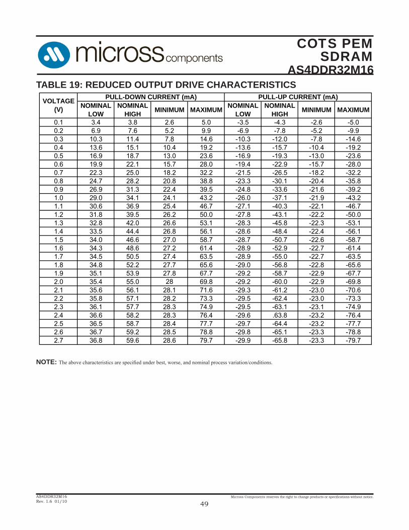
COTS PEMSDRAM
AS4DDR32M16
Micross Components reserves the right to change products or specifi cations without notice.
49AS4DDR32M16Rev. 1.6 01/10
TABLE 19: REDUCED OUTPUT DRIVE CHARACTERISTICS
NOTE: The above characteristics are specifi ed under best, worse, and nominal process variation/conditions.
NOMINALLOW
NOMINALHIGH MINIMUM MAXIMUM NOMINAL
LOWNOMINAL
HIGH MINIMUM MAXIMUM
0.1 3.4 3.8 2.6 5.0 -3.5 -4.3 -2.6 -5.00.2 6.9 7.6 5.2 9.9 -6.9 -7.8 -5.2 -9.90.3 10.3 11.4 7.8 14.6 -10.3 -12.0 -7.8 -14.60.4 13.6 15.1 10.4 19.2 -13.6 -15.7 -10.4 -19.20.5 16.9 18.7 13.0 23.6 -16.9 -19.3 -13.0 -23.60.6 19.9 22.1 15.7 28.0 -19.4 -22.9 -15.7 -28.00.7 22.3 25.0 18.2 32.2 -21.5 -26.5 -18.2 -32.20.8 24.7 28.2 20.8 38.8 -23.3 -30.1 -20.4 -35.80.9 26.9 31.3 22.4 39.5 -24.8 -33.6 -21.6 -39.21.0 29.0 34.1 24.1 43.2 -26.0 -37.1 -21.9 -43.21.1 30.6 36.9 25.4 46.7 -27.1 -40.3 -22.1 -46.71.2 31.8 39.5 26.2 50.0 -27.8 -43.1 -22.2 -50.01.3 32.8 42.0 26.6 53.1 -28.3 -45.8 -22.3 -53.11.4 33.5 44.4 26.8 56.1 -28.6 -48.4 -22.4 -56.11.5 34.0 46.6 27.0 58.7 -28.7 -50.7 -22.6 -58.71.6 34.3 48.6 27.2 61.4 -28.9 -52.9 -22.7 -61.41.7 34.5 50.5 27.4 63.5 -28.9 -55.0 -22.7 -63.51.8 34.8 52.2 27.7 65.6 -29.0 -56.8 -22.8 -65.61.9 35.1 53.9 27.8 67.7 -29.2 -58.7 -22.9 -67.72.0 35.4 55.0 28 69.8 -29.2 -60.0 -22.9 -69.82.1 35.6 56.1 28.1 71.6 -29.3 -61.2 -23.0 -70.62.2 35.8 57.1 28.2 73.3 -29.5 -62.4 -23.0 -73.32.3 36.1 57.7 28.3 74.9 -29.5 -63.1 -23.1 -74.92.4 36.6 58.2 28.3 76.4 -29.6 .63.8 -23.2 -76.42.5 36.5 58.7 28.4 77.7 -29.7 -64.4 -23.2 -77.72.6 36.7 59.2 28.5 78.8 -29.8 -65.1 -23.3 -78.82.7 36.8 59.6 28.6 79.7 -29.9 -65.8 -23.3 -79.7
VOLTAGE(V)
PULL-DOWN CURRENT (mA) PULL-UP CURRENT (mA)
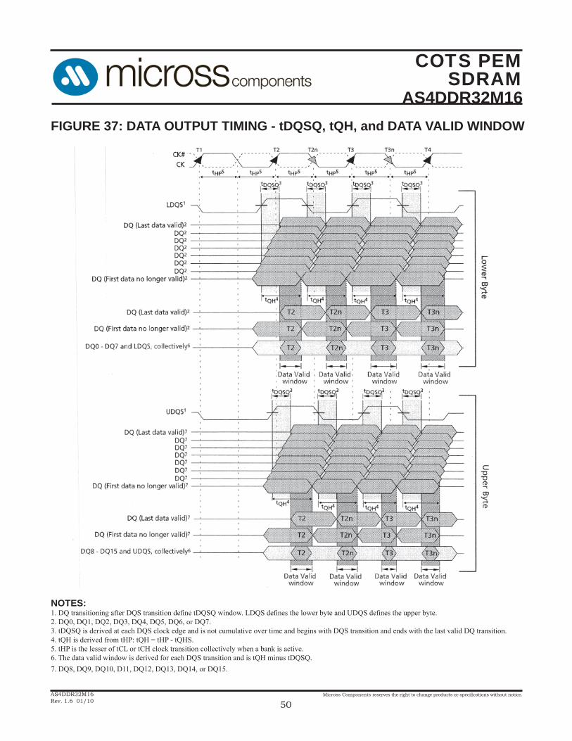
COTS PEMSDRAM
AS4DDR32M16
Micross Components reserves the right to change products or specifi cations without notice.
50AS4DDR32M16Rev. 1.6 01/10
FIGURE 37: DATA OUTPUT TIMING - tDQSQ, tQH, and DATA VALID WINDOW
NOTES:1. DQ transitioning after DQS transition defi ne tDQSQ window. LDQS defi nes the lower byte and UDQS defi nes the upper byte.2. DQ0, DQ1, DQ2, DQ3, DQ4, DQ5, DQ6, or DQ7.3. tDQSQ is derived at each DQS clock edge and is not cumulative over time and begins with DQS transition and ends with the last valid DQ transition.4. tQH is derived from tHP: tQH = tHP - tQHS.5. tHP is the lesser of tCL or tCH clock transition collectively when a bank is active.6. The data valid window is derived for each DQS transition and is tQH minus tDQSQ.7. DQ8, DQ9, DQ10, D11, DQ12, DQ13, DQ14, or DQ15.
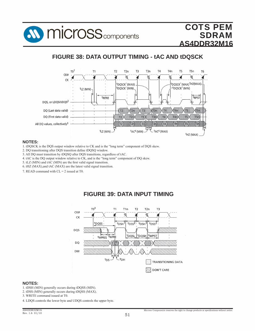
COTS PEMSDRAM
AS4DDR32M16
Micross Components reserves the right to change products or specifi cations without notice.
51AS4DDR32M16Rev. 1.6 01/10
FIGURE 38: DATA OUTPUT TIMING - tAC AND tDQSCK
NOTES:1. tDQSCK is the DQS output window relative to CK and is the “long term” component of DQS skew.2. DQ transitioning after DQS transition defi ne tDQSQ window.3. All DQ must transition by tDQSQ after DQS transitions, regardless of tAC.4. tAC is the DQ output window relative to CK, and is the “long term” component of DQ skew.5. tLZ (MIN) and tAC (MIN) are the fi rst valid signal transition.6. tHZ (MAX),and tAC (MAX) are the latest valid signal transition.7. READ command with CL = 2 issued at T0.
FIGURE 39: DATA INPUT TIMING
NOTES:1. tDSH (MIN) generally occurs during tDQSS (MIN).2. tDSS (MIN) generally occurs during tDQSS (MAX).3. WRITE command issued at T0.4. LDQS controls the lower byte and UDQS controls the upper byte.
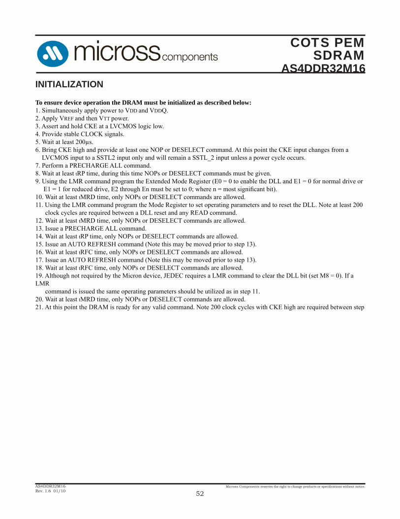
COTS PEMSDRAM
AS4DDR32M16
Micross Components reserves the right to change products or specifi cations without notice.
52AS4DDR32M16Rev. 1.6 01/10
To ensure device operation the DRAM must be initialized as described below:1. Simultaneously apply power to VDD and VDDQ.2. Apply VREF and then VTT power.3. Assert and hold CKE at a LVCMOS logic low.4. Provide stable CLOCK signals.5. Wait at least 200μs.6. Bring CKE high and provide at least one NOP or DESELECT command. At this point the CKE input changes from a LVCMOS input to a SSTL2 input only and will remain a SSTL_2 input unless a power cycle occurs.7. Perform a PRECHARGE ALL command.8. Wait at least tRP time, during this time NOPs or DESELECT commands must be given.9. Using the LMR command program the Extended Mode Register (E0 = 0 to enable the DLL and E1 = 0 for normal drive or E1 = 1 for reduced drive, E2 through En must be set to 0; where n = most signifi cant bit).10. Wait at least tMRD time, only NOPs or DESELECT commands are allowed.11. Using the LMR command program the Mode Register to set operating parameters and to reset the DLL. Note at least 200 clock cycles are required between a DLL reset and any READ command.12. Wait at least tMRD time, only NOPs or DESELECT commands are allowed.13. Issue a PRECHARGE ALL command.14. Wait at least tRP time, only NOPs or DESELECT commands are allowed.15. Issue an AUTO REFRESH command (Note this may be moved prior to step 13).16. Wait at least tRFC time, only NOPs or DESELECT commands are allowed.17. Issue an AUTO REFRESH command (Note this may be moved prior to step 13).18. Wait at least tRFC time, only NOPs or DESELECT commands are allowed.19. Although not required by the Micron device, JEDEC requires a LMR command to clear the DLL bit (set M8 = 0). If a LMR command is issued the same operating parameters should be utilized as in step 11.20. Wait at least tMRD time, only NOPs or DESELECT commands are allowed.21. At this point the DRAM is ready for any valid command. Note 200 clock cycles with CKE high are required between step
INITIALIZATION
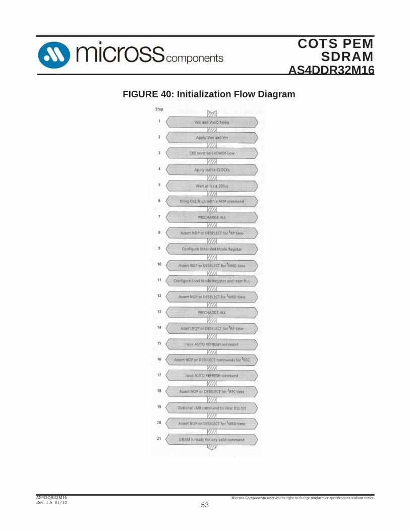
COTS PEMSDRAM
AS4DDR32M16
Micross Components reserves the right to change products or specifi cations without notice.
53AS4DDR32M16Rev. 1.6 01/10
FIGURE 40: Initialization Flow Diagram
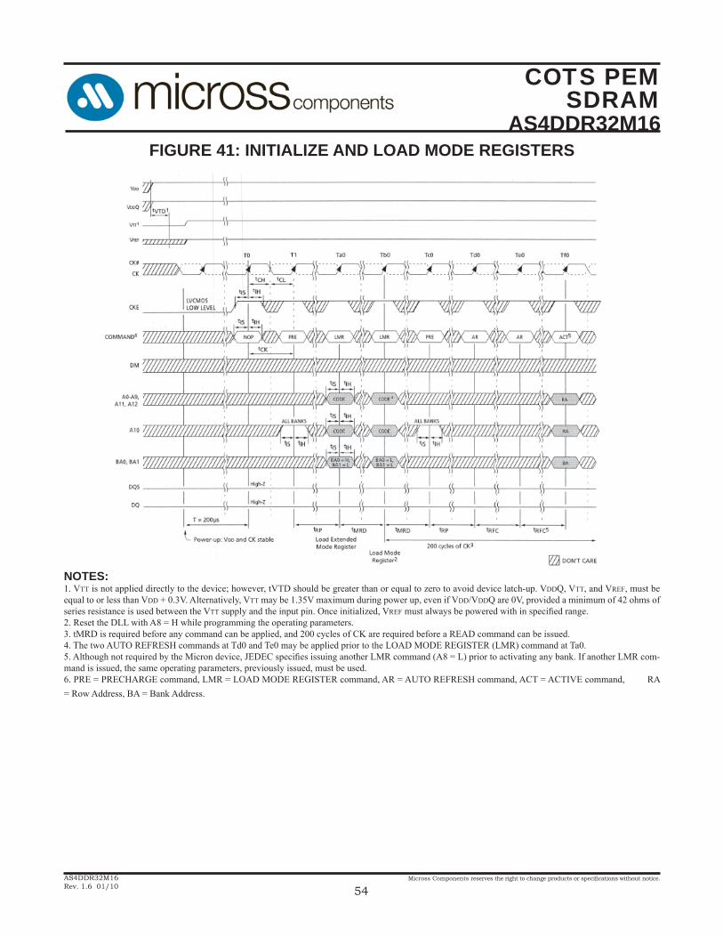
COTS PEMSDRAM
AS4DDR32M16
Micross Components reserves the right to change products or specifi cations without notice.
54AS4DDR32M16Rev. 1.6 01/10
FIGURE 41: INITIALIZE AND LOAD MODE REGISTERS
NOTES:1. VTT is not applied directly to the device; however, tVTD should be greater than or equal to zero to avoid device latch-up. VDDQ, VTT, and VREF, must be equal to or less than VDD + 0.3V. Alternatively, VTT may be 1.35V maximum during power up, even if VDD/VDDQ are 0V, provided a minimum of 42 ohms of series resistance is used between the VTT supply and the input pin. Once initialized, VREF must always be powered with in specifi ed range.2. Reset the DLL with A8 = H while programming the operating parameters.3. tMRD is required before any command can be applied, and 200 cycles of CK are required before a READ command can be issued.4. The two AUTO REFRESH commands at Td0 and Te0 may be applied prior to the LOAD MODE REGISTER (LMR) command at Ta0.5. Although not required by the Micron device, JEDEC specifi es issuing another LMR command (A8 = L) prior to activating any bank. If another LMR com-mand is issued, the same operating parameters, previously issued, must be used.6. PRE = PRECHARGE command, LMR = LOAD MODE REGISTER command, AR = AUTO REFRESH command, ACT = ACTIVE command, RA = Row Address, BA = Bank Address.
COTS PEMSDRAM
AS4DDR32M16
Micross Components reserves the right to change products or specifi cations without notice.
55AS4DDR32M16Rev. 1.6 01/10
FIGURE 42: POWER-DOWN MODE
NOTES:1. Once initialized, VREF must always be powered with in specifi ed range.2. If this command is a PRECHARGE (or if the device is already in the idle state), then the power-down mode shown is precharge power-down. If this com-mand is an ACTIVE (or if at least one row is already active), then the power-down mode shown is active power-down.3. No column accesses are allowed to be in progress at the time power-down is entered.
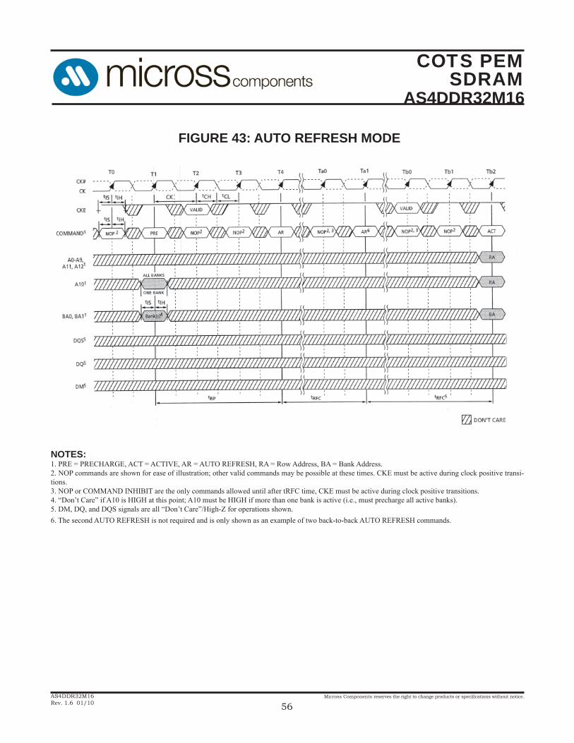
COTS PEMSDRAM
AS4DDR32M16
Micross Components reserves the right to change products or specifi cations without notice.
56AS4DDR32M16Rev. 1.6 01/10
FIGURE 43: AUTO REFRESH MODE
NOTES:1. PRE = PRECHARGE, ACT = ACTIVE, AR = AUTO REFRESH, RA = Row Address, BA = Bank Address.2. NOP commands are shown for ease of illustration; other valid commands may be possible at these times. CKE must be active during clock positive transi-tions.3. NOP or COMMAND INHIBIT are the only commands allowed until after tRFC time, CKE must be active during clock positive transitions.4. “Don’t Care” if A10 is HIGH at this point; A10 must be HIGH if more than one bank is active (i.e., must precharge all active banks).5. DM, DQ, and DQS signals are all “Don’t Care”/High-Z for operations shown.6. The second AUTO REFRESH is not required and is only shown as an example of two back-to-back AUTO REFRESH commands.
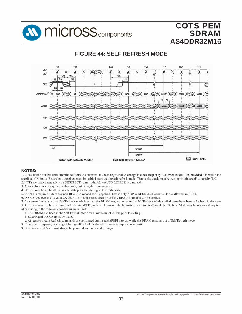
COTS PEMSDRAM
AS4DDR32M16
Micross Components reserves the right to change products or specifi cations without notice.
57AS4DDR32M16Rev. 1.6 01/10
FIGURE 44: SELF REFRESH MODE
NOTES:1. Clock must be stable until after the self refresh command has been registered. A change in clock frequency is allowed before Ta0, provided it is within the specifi ed tCK limits. Regardless, the clock must be stable before exiting self refresh mode. That is, the clock must be cycling within specifi cations by Ta0.2. NOPs are interchangeable with DESELECT commands, AR = AUTO REFRESH command.3. Auto Refresh is not required at this point, but is highly recommended.4. Device must be in the all banks idle state prior to entering self refresh mode.5. tXSNR is required before any non-READ command can be applied. That is only NOP or DESELECT commands are allowed until Tb1.6. tXSRD (200 cycles of a valid CK and CKE = high) is required before any READ command can be applied.7. As a general rule, any time Self Refresh Mode is exited, the DRAM may not re-enter the Self Refresh Mode until all rows have been refreshed via the Auto Refresh command at the distributed refresh rate, tREFI, or faster. However, the following exception is allowed. Self Refresh Mode may be re-entered anytime after exiting, if the following conditions are all met:
a. The DRAM had been in the Self Refresh Mode for a minimum of 200ms prior to exiting.b. tXSNR and tXSRD are not violated.c. At least two Auto Refresh commands are performed during each tREFI interval while the DRAM remains out of Self Refresh mode.
8. If the clock frequency is changed during self refresh mode, a DLL reset is required upon exit.9. Once initialized, Vref must always be powered with in specifi ed range.
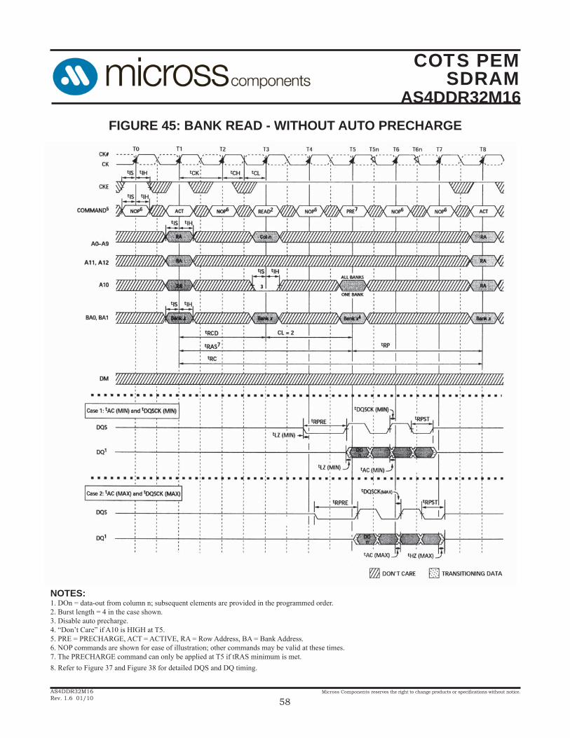
COTS PEMSDRAM
AS4DDR32M16
Micross Components reserves the right to change products or specifi cations without notice.
58AS4DDR32M16Rev. 1.6 01/10
FIGURE 45: BANK READ - WITHOUT AUTO PRECHARGE
NOTES:1. DOn = data-out from column n; subsequent elements are provided in the programmed order.2. Burst length = 4 in the case shown.3. Disable auto precharge.4. “Don’t Care” if A10 is HIGH at T5.5. PRE = PRECHARGE, ACT = ACTIVE, RA = Row Address, BA = Bank Address.6. NOP commands are shown for ease of illustration; other commands may be valid at these times.7. The PRECHARGE command can only be applied at T5 if tRAS minimum is met.8. Refer to Figure 37 and Figure 38 for detailed DQS and DQ timing.
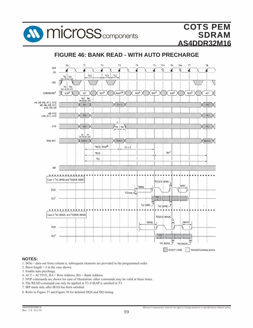
COTS PEMSDRAM
AS4DDR32M16
Micross Components reserves the right to change products or specifi cations without notice.
59AS4DDR32M16Rev. 1.6 01/10
FIGURE 46: BANK READ - WITH AUTO PRECHARGE
NOTES:1. DOn = data-out from column n; subsequent elements are provided in the programmed order.2. Burst length = 4 in the case shown.3. Enable auto precharge.4. ACT = ACTIVE, RA = Row Address, BA = Bank Address.5. NOP commands are shown for ease of illustration; other commands may be valid at these times.6. The READ command can only be applied at T3 if tRAP is satisfi ed at T3.7. tRP starts only after tRAS has been satisfi ed.8. Refer to Figure 37 and Figure 38 for detailed DQS and DQ timing.
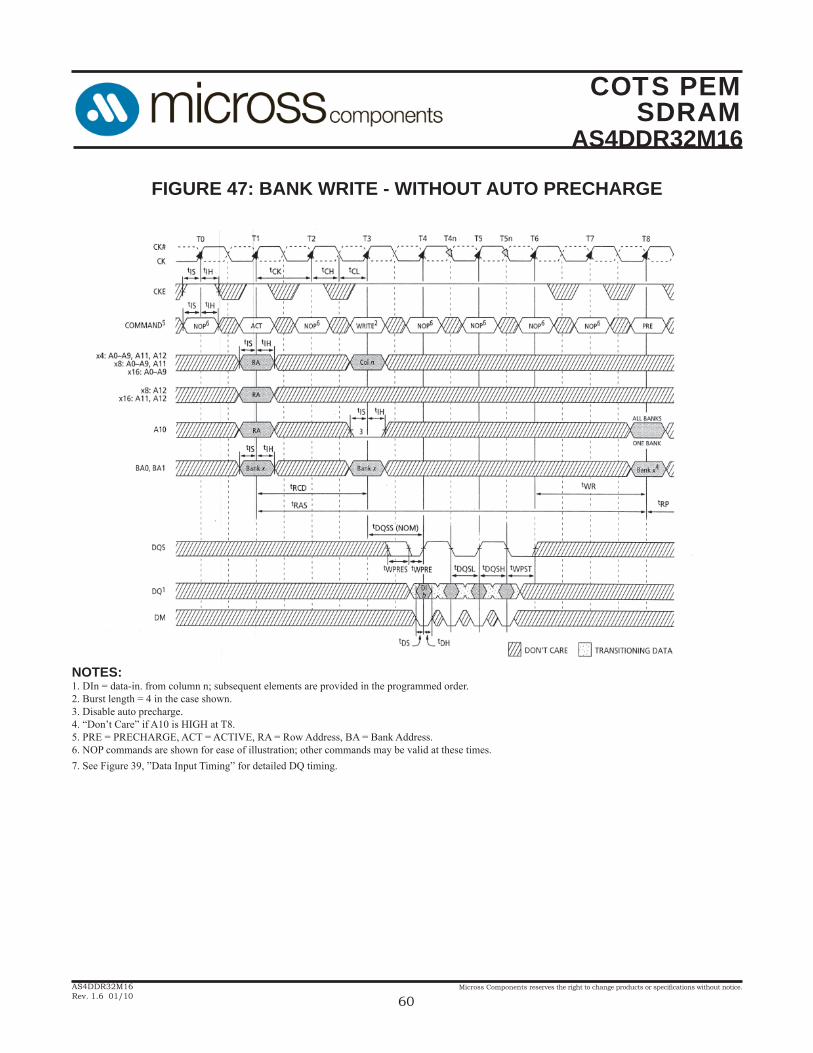
COTS PEMSDRAM
AS4DDR32M16
Micross Components reserves the right to change products or specifi cations without notice.
60AS4DDR32M16Rev. 1.6 01/10
FIGURE 47: BANK WRITE - WITHOUT AUTO PRECHARGE
NOTES:1. DIn = data-in. from column n; subsequent elements are provided in the programmed order.2. Burst length = 4 in the case shown.3. Disable auto precharge.4. “Don’t Care” if A10 is HIGH at T8.5. PRE = PRECHARGE, ACT = ACTIVE, RA = Row Address, BA = Bank Address.6. NOP commands are shown for ease of illustration; other commands may be valid at these times.7. See Figure 39, ”Data Input Timing” for detailed DQ timing.
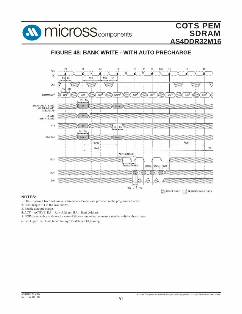
COTS PEMSDRAM
AS4DDR32M16
Micross Components reserves the right to change products or specifi cations without notice.
61AS4DDR32M16Rev. 1.6 01/10
FIGURE 48: BANK WRITE - WITH AUTO PRECHARGE
NOTES:1. DIn = data-out from column n; subsequent elements are provided in the programmed order.2. Burst length = 4 in the case shown.3. Enable auto precharge.4. ACT = ACTIVE, RA = Row Address, BA = Bank Address.5. NOP commands are shown for ease of illustration; other commands may be valid at these times.6. See Figure 39, ”Data Input Timing” for detailed DQ timing.
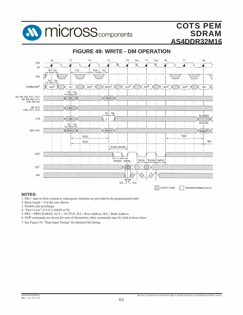
COTS PEMSDRAM
AS4DDR32M16
Micross Components reserves the right to change products or specifi cations without notice.
62AS4DDR32M16Rev. 1.6 01/10
FIGURE 49: WRITE - DM OPERATION
NOTES:1. DIn = data-in from column n; subsequent elements are provided in the programmed order.2. Burst length = 4 in the case shown.3. Disable auto precharge.4. “Don’t Care” if A10 is HIGH at T8.5. PRE = PRECHARGE, ACT = ACTIVE, RA = Row Address, BA = Bank Address.6. NOP commands are shown for ease of illustration; other commands may be valid at these times.7. See Figure 39, ”Data Input Timing” for detailed DQ timing.
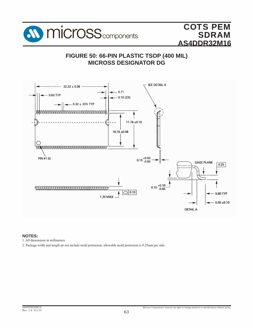
COTS PEMSDRAM
AS4DDR32M16
Micross Components reserves the right to change products or specifi cations without notice.
63AS4DDR32M16Rev. 1.6 01/10
FIGURE 50: 66-PIN PLASTIC TSOP (400 MIL)MICROSS DESIGNATOR DG
NOTES:1. All dimensions in millimeters2. Package width and length do not include mold protrusion; allowable mold protrusion is 0.25mm per side.
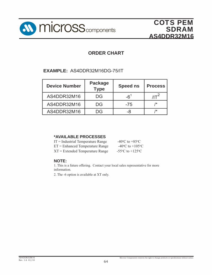
COTS PEMSDRAM
AS4DDR32M16
Micross Components reserves the right to change products or specifi cations without notice.
64AS4DDR32M16Rev. 1.6 01/10
ORDER CHART
EXAMPLE: AS4DDR32M16DG-75/IT
Device Number PackageType Speed ns Process
AS4DDR32M16 DG -61 /IT2
AS4DDR32M16 DG -75 /*AS4DDR32M16 DG -8 /*
*AVAILABLE PROCESSESIT = Industrial Temperature Range -40oC to +85oCET = Enhanced Temperature Range -40oC to +105oCXT = Extended Temperature Range -55oC to +125oC
NOTE: 1. This is a future offering. Contact your local sales representative for more information.2. The -6 option is available at XT only.