Embed Size (px)
Citation preview

Copyright
by
Zhiquan Luo
2009
The Dissertation Committee for Zhiquan Luo
Certifies that this is the approved version of the following dissertation:
Nanoindentation Study of Buckling and Friction of Silicon Nanolines
Committee:
Paul S. Ho, Supervisor
Ernst-Ludwig Florin
Chih-Kang Shih
Zhen Yao
Wolfgang Frey
Nanoindentation Study of Buckling and Friction of Silicon Nanolines
By
Zhiquan Luo, B.S.; M.S.
Dissertation
Presented to the Faculty of the Graduate School of
The University of Texas at Austin
in Partial Fulfillment
of the Requirements
for the Degree of
Doctor of Philosophy
The University of Texas at Austin
May, 2009
Dedication
To my wife, Xiaoning Liu and my son, Daniel Luo

v
Acknowledgements
I would like to express my gratitude to all those who gave me the possibility to
complete this thesis. During the last several years, I had enormous help and support from
many friends and teachers. Without them, I would not finish my degree at the University
of Texas at Austin. First, I am deeply indebted to my advisor, Prof. Paul S. Ho. Without
Dr. Ho’s continuous support and advice, both professionally and personally, thought out
my doctoral work, I was unable to make progress toward the finishing of my degree. I
would like to extend my sincere appreciation to all my graduate committee members,
Prof. Chih-Kang Shih, Prof. Ernst-Ludwig Florin, Prof. Zhen Yao, and Prof. Wolfgang
Frey for serving the committee and their support and encouragement. I specially thank
Dr. Jang-Hi Im for his continuous support and advice throughout my doctoral work;
thank Dr. Ryan Scott Smith and Dr. Bin Li for numerous suggestions and invaluable help
on my thesis.
I also want to take this opportunity to thank my colleagues and friends in the
Laboratory for Interconnect and Packaging for their advice and discussions about my
research. I am thankful to Ms. Jo Ann Smith for her help, and to all my friends on the J.J.
Pickle research campus for their warm friendship.
Last but not least, I’d like to thank my family. I can not be thankful enough to my
wife, Xiaoning Liu, for her endless love and continuous encouragement and patience. I
am also thankful to my parents-in-law and parents for supporting me to accomplish this
work. Especially, I would like to give my special thanks to Mr. Yuan’s family for their
generous help all the time.
vi
Nanoindentation Study of Buckling and Friction of Silicon Nanolines
Publication No._____________
Zhiquan Luo, Ph.D.
The University of Texas at Austin, 2009
Supervisor: Paul S. Ho
Silicon-based nanostructures are essential building blocks for nanoelectronic
devices and nano-electromechanical systems (NEMS). As the silicon device size
continues to scale down, the surface to volume ratio becomes larger, rendering the
properties of surfaces and interfaces more important for improving the properties of the
nano-devices and systems. One of those properties is the friction, which is important in
controlling the functionality and reliability of the nano-device and systems. The goal of
this dissertation is to investigate the deformation and friction behaviors of single
crystalline silicon nanolines (SiNLs) using nanoindentation techniques.
Following an introduction and a summary of the theoretical background of
contact friction in Chapters 1 and 2, the results of this thesis are presented in three
chapters. In Chapter 3, the fabrication of the silicon nanolines is described. The
fabrication method yielded high-quality single-crystals with line width ranging from
30nm to 90nm and height to width aspect ratio ranging from 10 to 25. These SiNL
structures have properties and dimensions well suited for the study of the mechanical and
vii
friction behaviors at the nanoscale. In Chapter 4, we describe the study of the mechanical
properties of SiNLs using the nanoindentation method. The loading-displacement curves
show that the critical load to induce the buckling of the SiNLs can be correlated to the
contact friction and geometry of SiNLs. A map was built as a guideline to describe the
selection of buckling modes. The map was divided into three regions where different
regions correlate to different buckling modes including Mode I, Mode II and sliding-
bending of SiNLs. In Chapter 5, we describe the study of the contact friction of the SiNL
structures. The friction coefficient at the contact was extracted from the load-
displacement curves. Subsequently, the frictional shear stress was evaluated. In addition,
the effect of the interface between the indenter and SiNLs was investigated using SiNLs
with surfaces coated by a thin silicon dioxide or chromium film. The material of the
interface was found to influence significantly the contact friction and its behavior. Cyclic
loading-unloading experiments showed the friction coefficient dramatically changed after
only a few loading cycles, indicating the contact history is important in controlling the
friction behaviors of SiNLs at nanoscales. This thesis is concluded with a summary of the
results and proposed future studies.
viii
Table of Contents
List of Tables ........................................................................................................... x
List of Figures ........................................................................................................ xi
Chapter 1: Introduction ........................................................................................ 1
1.1 Challenges of Fabrication and Characterization of Nano-structures .... 4
1.2 Mechanical Characterization of Nano-structures .................................. 7
1.3 Nanofriction of SiNLs ........................................................................... 9
1.4 Objective and Organization of Dissertation ........................................ 12
Chapter 2: Contact Mechanics and Compressive Instability of Columns .......... 14
2.1 Contact Mechanics of a Sphere pressed into a Half-space.................. 15
2.1.l Adhesionless Contact Mechanics - Hertzian Model[66] ............ 15
2.1.2 Adhesive Contact Mechanics ..................................................... 17
2.2 Compressive Instability of Columns ................................................... 22
Chapter 3: Experimental Techniques ................................................................. 27
3.1 Fabrication of SiNL Test Structures ................................................... 27
3.1.1 Electron Beam Lithography Technique ..................................... 28
3.1.2 RIE and Pattern Transfer Process .............................................. 32
3.1.3 Anisotropic Wet Etching (AWE) Process .................................. 33
3.1.4 SiNL Structure Design and Fabrication Results ........................ 34
3.1.5 Coating of SiNLs with Silicon Dioxide and Chromium ............ 40
3.2 NanoMechanical Testing System ........................................................ 41
Chapter 4: Analysis of Buckling Behavior of SiNLs ......................................... 45
4.1 FEM Simulation of Nanoindentation on SiNLs .................................. 46
4.1.1 FEM Model ................................................................................ 46
4.1.2 FEM Simulation Results for 75nm SiNLs ................................. 48
4.2 Analysis of Experimental Load-Displacement Curves ....................... 50
4.3 Buckling Response Analysis ............................................................... 55
4.3.1 Formulation of the Problem ....................................................... 56
ix
4.3.2 Buckling Modes and Critical Loads Analysis ............................ 58
4.3.3 The Effect of Geometry and Friction on Buckling Behavior ..... 65
4.4 Summary ............................................................................................. 69
Chapter 5: Frictional Behaviors of SiNLs .......................................................... 70
5.1 Introduction to Test Structures and Test Ambient .............................. 70
5.1.1 Test Structures ............................................................................ 71
5.1.2 Impact of Test ambient on Friction at contact............................ 73
5.2 Contact Area Evaluation ..................................................................... 77
5.2.1 Formulation of the problem........................................................ 77
5.2.2 Calculation of Contact Area ....................................................... 79
5.2.3 Calculation of Penetration Depth by indentation Displacement 82
5.2.4 Calculation of Penetration Depth by Normal Force ................... 85
5.3 Friction of Bare SiNLs ........................................................................ 86
5.3.1 Experimental results for 90nm and 75nm SiNLs test structures 86
5.3.2 Experimental results for 60nm/610nm and 30nm/720nm SiNLs90
5.4 Friction of Coated SiNLs .................................................................... 94
5.5 Friction of SiNLs under cyclic loading ............................................... 98
5.6 Summary ........................................................................................... 104
Chapter 6: Summary and Future Work ............................................................ 106
6.1 Summary ........................................................................................... 106
6.2 Future Work ...................................................................................... 108
Selected Publications........................................................................................... 111
References ........................................................................................................... 112
Vita .................................................................................................................... 120
x
List of Tables
Table 4.1 Coefficient of Friction Required for Mode II Buckling ................................ 68
Table 5.1 Specifics of 5 sets of test structures and coating layers. Test conditions are also summarized. The thickness of silicon oxide and chromium layers were around 3nm and 2nm respectively. ...................................................................... 72
Table 5.2 Critical Loads of 70nm/610nm SiNLs under dry and ambient test conditions ............................................................................................................. 75
Table 5.3 Critical loads and friction coefficients of 90nm bare SiNLs......................... 88
Table 5.4 Frictional Shear Stress of 90nm SiNLs ......................................................... 90
Table 5.5 Frictional Shear Stress of 75nm SiNLs ......................................................... 90
Table 5.6 Summary of critical loads and friction coefficient ........................................ 91
Table 5.7 Average critical loads and friction coefficient of 75nm SiNLs with or without coating layers. ......................................................................................... 95
Table 5.8 Critical loads and friction coefficients of 90nm SiNLs under a 4-cycle loading experiment ............................................................................................... 99
xi
List of Figures
Figure 1.1 Application of silicon nanowires in a dual-gate NWFET with Silicided contact. ................................................................................................................... 2
Figure 1.2 (a) Plan view SEM image of SiNWs formed by VLS process [21]. (b) Cross-sectional SEM image of lateral epitaxial SiNWs grown between microtrench by MCCVD process. .......................................................................... 5
Figure 1.3 (a) 12 nm wide SiNWs generated by SNAP process. Pattern was transferred into silicon using CF4+O2 plasma etching, showing line roughness due to ion bombardment. The scale bar in the inset is 150 nm. (b) SEM image of feature cross-sections of silicon lines after KOH wet etching on (110) Si wafer. The silicon nitride hard-mask caps had not been removed .................................... 6
Figure 1.4 Schematic of experiments setup, a) before and b) after the manipulation. .... 8
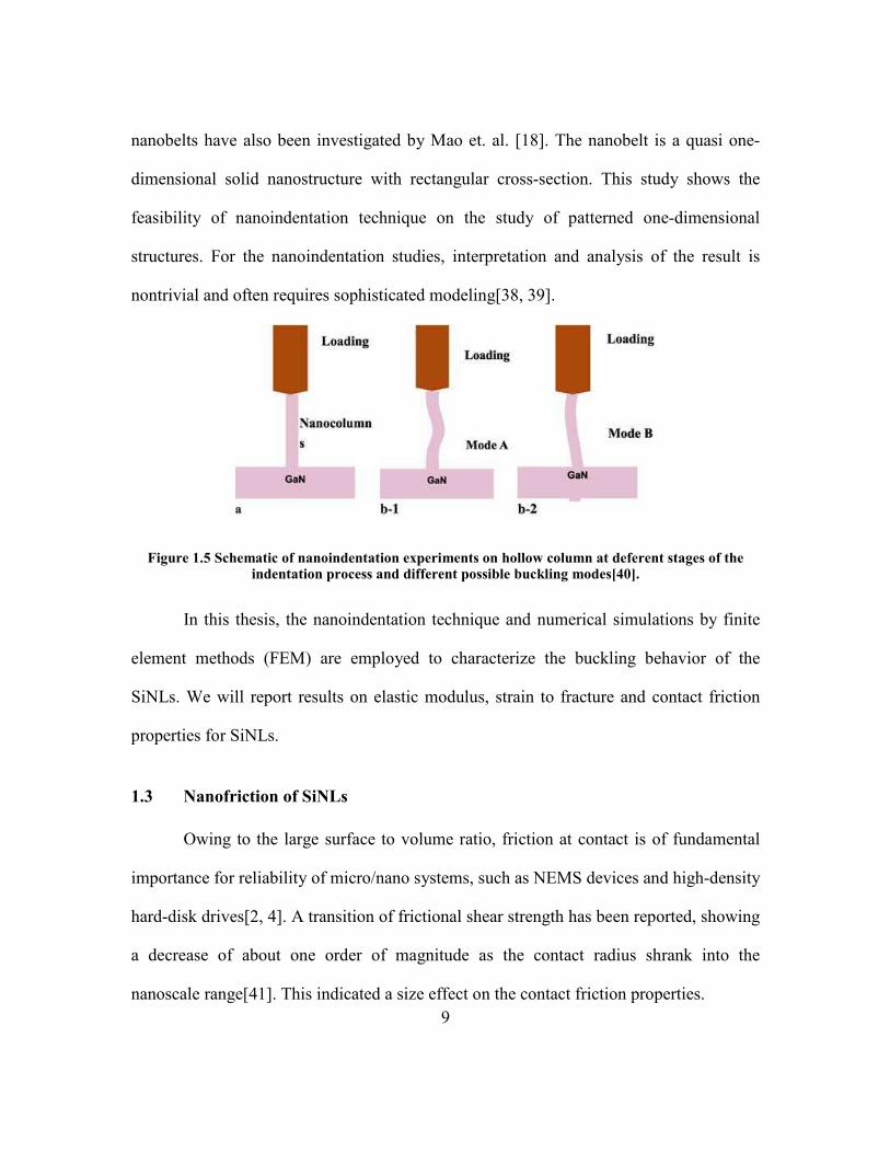
Figure 1.5 Schematic of nanoindentation experiments on hollow column at deferent stages of the indentation process and different possible buckling modes. ........... 9
Figure 2.1 Geometry of the Hertzian model before contact a) and after contact b). ..... 17
Figure 2.2 Geometry of the DMT adhesive contact. The attractive interactions act outside the contact zone ....................................................................................... 19
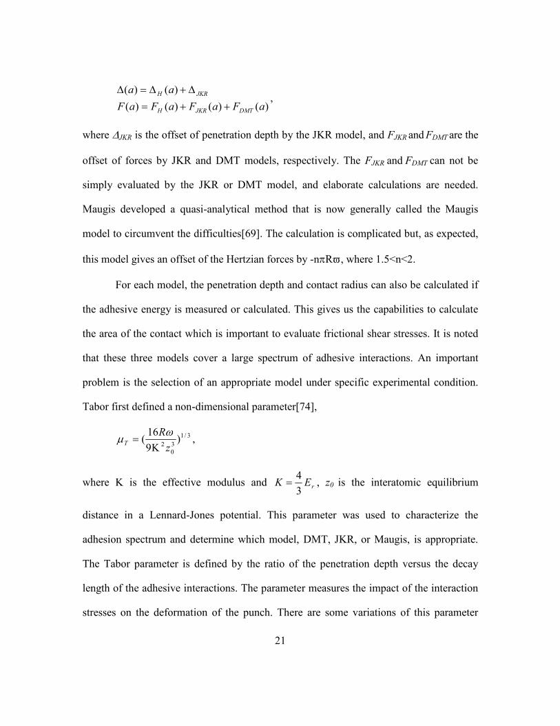
Figure 2.3 Schematic illustration of JKR adhesive contact. The existing of adhesive forces changes the area of the contact zone which is shown by the formation of “necking” in a) outside of the contact zone denoted by dashed curve. In order to keep the area of contact zone constant under this case, a negative force is need to “pull out” the punch a little which is shown in b). ........................................... 20
Figure 2.4 Beam-column structures with axial and transverse load. a) with both ends fixed; b) with one end fixed and the other end hinged; c) with both ends hinged.25
Figure 3.1 Layer stack of EBL substrate. ...................................................................... 30
xii
Figure 3.2 The effect of dosage levels on the line width of SiNLs. Left, under-dosed exposure leaving more materials unremoved in the trench area (dark), and resulted in larger line width (brighter). Right, over-dosed exposure removed more materials from the trench area, and SiNLs structures with smaller line width were obtained. ............................................................................................ 31
Figure 3.3 Difference between anisotropic etching and isotropic etching. ................... 34
Figure 3.4 a) Schematic of the mask design of SiNLs. b) A trench was formed by AWE. c) Schematic of cross-section of a trench. d) Formation of a SiNL between two trenches. .......................................................................................... 36
Figure 3.5 The silicon nanoline arrays fabricated by EBL and AWE. a) Grating pattern of in array element; b) SEM image of SiNLs structures after AWE. c) Pattern array for orientation alignment. ............................................................... 38
Figure 3.6 Schematic of undercut and line width control. ............................................ 39
Figure 3.7 Cross-sectional SEM images of some Si nanoline arrays fabricated by EBL+AWE. (a) 30 nm wide lines with height of ∼ 350 nm; (b) 65nm wide lines with height of ∼ 1 µm. (c) 1500 nm wide lines with height of ∼ 560 nm. ........... 40
Figure 3.8 Schematic of an AFM based nano-indentation process ............................... 43
Figure 3.9 SEM images of three types of indenters. (a) Berkovich indenter, 3-Sided pyramidal shape, 142.6° (edge to opposing face), and ∼ 150 nm tip radius; (b) NorthStar indenter, 3-Sided pyramidal shape, Cube corner profile, and ∼ 50 nm tip radius; (c) Conical indenter, conical shape, 60° included angle and > 1 µm tip radius. .............................................................................................................. 43
Figure 3.10 Schematic of indentation technique for modulus and hardness measurement. (a) Indentation on surface of materials; (b) typical load vs. displacement curve recorded in the indentation process. ..................................... 44
Figure 4.1 Layout of the 3D FEM model of indentation on silicon nanolines. ............ 47
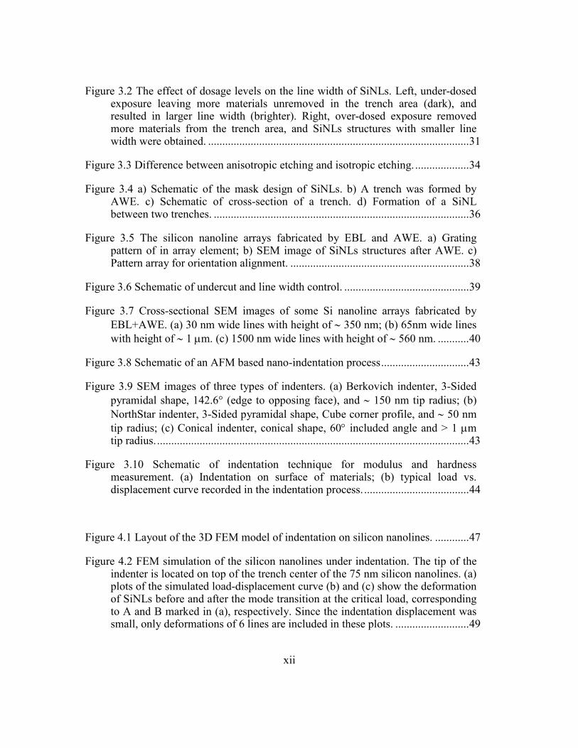
Figure 4.2 FEM simulation of the silicon nanolines under indentation. The tip of the indenter is located on top of the trench center of the 75 nm silicon nanolines. (a) plots of the simulated load-displacement curve (b) and (c) show the deformation of SiNLs before and after the mode transition at the critical load, corresponding to A and B marked in (a), respectively. Since the indentation displacement was small, only deformations of 6 lines are included in these plots. .......................... 49
xiii
Figure 4.3 The dependence of critical buckling load on the friction coefficients. When the friction coefficient increases, the height of the peak of the load-displacement curves increases indicating the increasing of critical buckling load. ................... 50
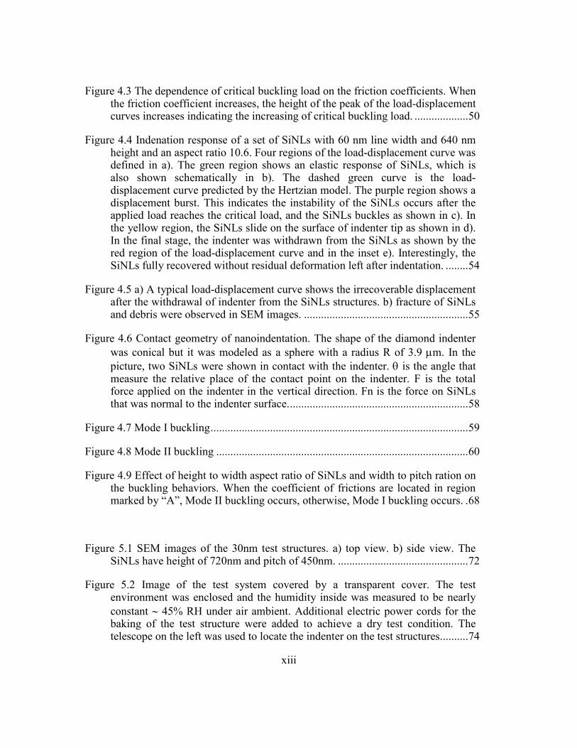
Figure 4.4 Indenation response of a set of SiNLs with 60 nm line width and 640 nm height and an aspect ratio 10.6. Four regions of the load-displacement curve was defined in a). The green region shows an elastic response of SiNLs, which is also shown schematically in b). The dashed green curve is the load-displacement curve predicted by the Hertzian model. The purple region shows a displacement burst. This indicates the instability of the SiNLs occurs after the applied load reaches the critical load, and the SiNLs buckles as shown in c). In the yellow region, the SiNLs slide on the surface of indenter tip as shown in d). In the final stage, the indenter was withdrawn from the SiNLs as shown by the red region of the load-displacement curve and in the inset e). Interestingly, the SiNLs fully recovered without residual deformation left after indentation. ........ 54
Figure 4.5 a) A typical load-displacement curve shows the irrecoverable displacement after the withdrawal of indenter from the SiNLs structures. b) fracture of SiNLs and debris were observed in SEM images. .......................................................... 55
Figure 4.6 Contact geometry of nanoindentation. The shape of the diamond indenter was conical but it was modeled as a sphere with a radius R of 3.9 µm. In the picture, two SiNLs were shown in contact with the indenter. θ is the angle that measure the relative place of the contact point on the indenter. F is the total force applied on the indenter in the vertical direction. Fn is the force on SiNLs that was normal to the indenter surface. ............................................................... 58
Figure 4.7 Mode I buckling ........................................................................................... 59
Figure 4.8 Mode II buckling ......................................................................................... 60
Figure 4.9 Effect of height to width aspect ratio of SiNLs and width to pitch ration on the buckling behaviors. When the coefficient of frictions are located in region marked by “A”, Mode II buckling occurs, otherwise, Mode I buckling occurs. . 68
Figure 5.1 SEM images of the 30nm test structures. a) top view. b) side view. The SiNLs have height of 720nm and pitch of 450nm. .............................................. 72
Figure 5.2 Image of the test system covered by a transparent cover. The test environment was enclosed and the humidity inside was measured to be nearly constant ∼ 45% RH under air ambient. Additional electric power cords for the baking of the test structure were added to achieve a dry test condition. The telescope on the left was used to locate the indenter on the test structures.......... 74
xiv
Figure 5.3 Image of the heating chip, sample stage, and the SiNLs test structures. The heating stage is consisted of a silicon chip with copper film resistor, which is sandwiched between the test structures and the sample stage. Temperature of the test structures was controlled by the DC power source. In the experiments, temperature up to 110°C was maintained for about 10 minutes to drive out moisture on the test structures. A humidity of less than 5% was measured after 3 hours of dry nitrogen gas flush afterwards. .......................................................... 75
Figure 5.4 The geometry of a diamond indenter on SiNLs structures before the indenter was brought into contact with the SiNLs. The tip of the indenter was placed at the center of the trench. ......................................................................... 78
Figure 5.5 Geometry configurations that are equivalent as the original contact geometry defined in Figure 5.3. Here, the system is defined as SiNLs “indenters” indent on a diamond half-space. The SiNLs originally having rectangular cross-section are now replace by SiNLs “indenters” with their top surfaces defined as spherical sectors. The spherical sectors have the same diameter as that of the original diamond indenter ................................................ 79
Figure 5.6 SiNLs indenters before contact a), and SiNLs being pressed into the diamond half-space b), but the contact zone size a is smaller than the line width w on the x direction, i. e. the contact is incomplete. ............................................ 83
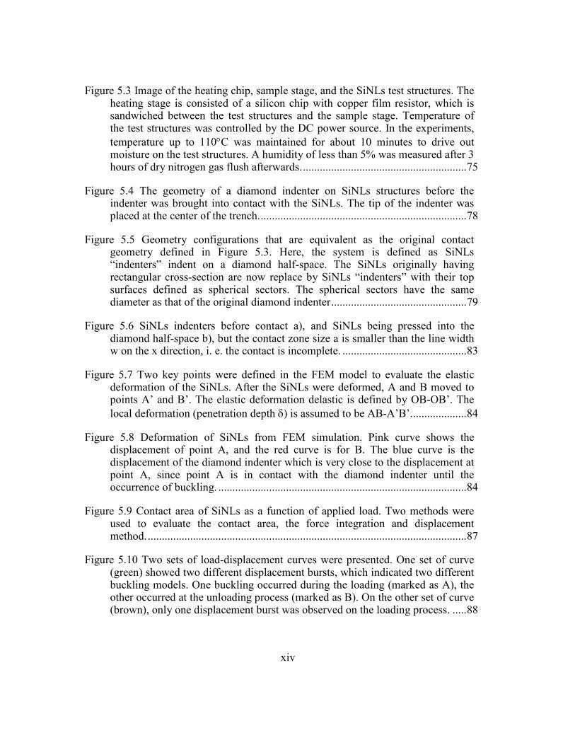
Figure 5.7 Two key points were defined in the FEM model to evaluate the elastic deformation of the SiNLs. After the SiNLs were deformed, A and B moved to points A’ and B’. The elastic deformation delastic is defined by OB-OB’. The local deformation (penetration depth δ) is assumed to be AB-A’B’. ................... 84
Figure 5.8 Deformation of SiNLs from FEM simulation. Pink curve shows the displacement of point A, and the red curve is for B. The blue curve is the displacement of the diamond indenter which is very close to the displacement at point A, since point A is in contact with the diamond indenter until the occurrence of buckling. ........................................................................................ 84
Figure 5.9 Contact area of SiNLs as a function of applied load. Two methods were used to evaluate the contact area, the force integration and displacement method. ................................................................................................................. 87
Figure 5.10 Two sets of load-displacement curves were presented. One set of curve (green) showed two different displacement bursts, which indicated two different buckling models. One buckling occurred during the loading (marked as A), the other occurred at the unloading process (marked as B). On the other set of curve (brown), only one displacement burst was observed on the loading process. ..... 88
xv
Figure 5.11 Average friction coefficients for test structures with width/height configurations of 90nm/1400nm, 75nm/1400nm, 60nm/610nm and 30nm/720nm......................................................................................................... 92
Figure 5.12 Average friction coefficients for test structures with width/height configurations of 90nm/1400nm, 75nm/1400nm, 60nm/610nm and 30nm/720nm......................................................................................................... 92
Figure 5.13 Typical load-displacement curve for the SiNLs of 60nm/610nm configuration. The critical load was 62 µN, and corresponding friction coefficient was 0.043............................................................................................ 93
Figure 5.14 Typical load-displacement curve for 30nm/720nm SiNLs. The critical load is 23.7µN, and corresponding friction coefficient is 0.042. ......................... 93
Figure 5.15 Typical load-displacement curves for 75nm/1400nm test structures with or without coating layers: blue curve for bare SiNLs with the highest critical load, red curve for SiNLs with oxide and green curve for SiNLs with chromium layer. ..................................................................................................................... 96
Figure 5.16 Comparison of the friction coefficients of SiNLs with different line widths and coatings. ............................................................................................. 97
Figure 5.17 Load function of multi-cycle loading indentation. Four cycles were designed with the same maximum loading forces for each loading cycle at 150 µN. The loading and unloading rates were also designed constant for each cycle at 75µN/second and -75µN/second, respectively. .............................................. 100
Figure 5.18 Load-displacement curves of 90nm SiNLs under multi-cycle loading. The load function was defined in Figure 5.17 with four total loading cycles and maximum loading forces of 150µN for all cycles. ............................................. 101
Figure 5.19 Friction coefficients on 90nm SiNLs after two runs of 4-cycle loading indentation on the same location. Data points in blue were generated by the first 4-cycle loading and the pink data points were generate by the second 4-cycle loading. The same load function shown in Figure 5.17 was used for both runs of 4-cycle loading indentation. ............................................................................... 102
Figure 5.20 Load-displacement curves for 60nm SiNLs with coatings under 4-cycle loading indentations. The critical loads of the second cycle clearly dropped from that of the first cycle. The decrease of critical load after the first cycle was more significant for bare SiNLs as shown in a), than that of SiNLs coated with silicon dioxide shown in b) and chromium shown in c). Load function shown in Figure 5.17 was used for all experiments. ..................................................................... 103
1
Chapter 1: Introduction
With the miniaturization of semi-conductor devices into the tens of nano-meter
scale, nanotechnology and nano-materials have been widely used in Nano-Electro-
Mechanical systems (NEMS)[1-3], and have a significant impact on our daily life.
Various applications include drug delivery, biomedicine field, chemical catalysis, solar
cell systems, spintronics, ultra large-scale integrated (ULSI) circuits, etc[4-6]. For
example, recently an Indian drug firm, Dabur Pharma, announced a new anti-cancer drug
delivery system, which is a nano-particle based system with feature size down to a few
nanometers[7]. The system allows for a more targeted treatment and avoids the unsafe
and unpleasant side effects of chemotherapy. Another example is in the biomedical field.
Nanopore technology can be applied to the analysis of nucleic acids converting
nucleotides directly into electronic signatures. This can be employed in tissue engineering
and lab-on-chip system to diagnose diseases[8] . In addition, due to the intrinsic large
surface area to volume ratio of nano-structures, platinum nanoparticles are being
considered as the next generation automotive catalytic converters, suggesting a great
potential of their application in chemical catalysis[9]. For industrial applications, as
CMOS technology is entering into the 32 nm node in 2009, nanotechnology, particularly
the immersion lithography and the related patterning process[10, 11], will be of critical
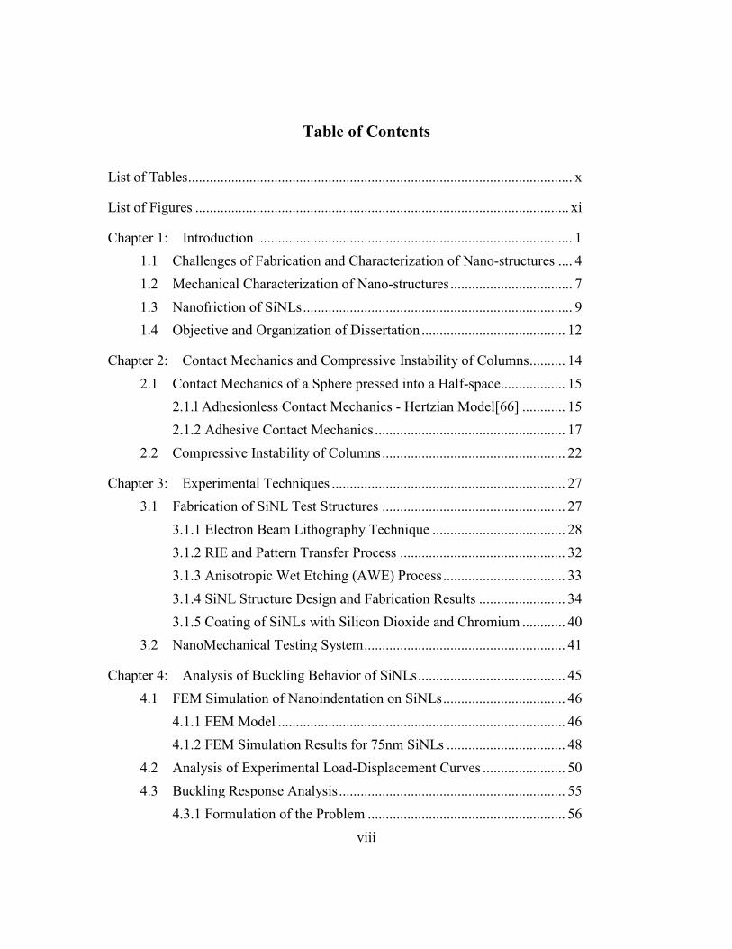
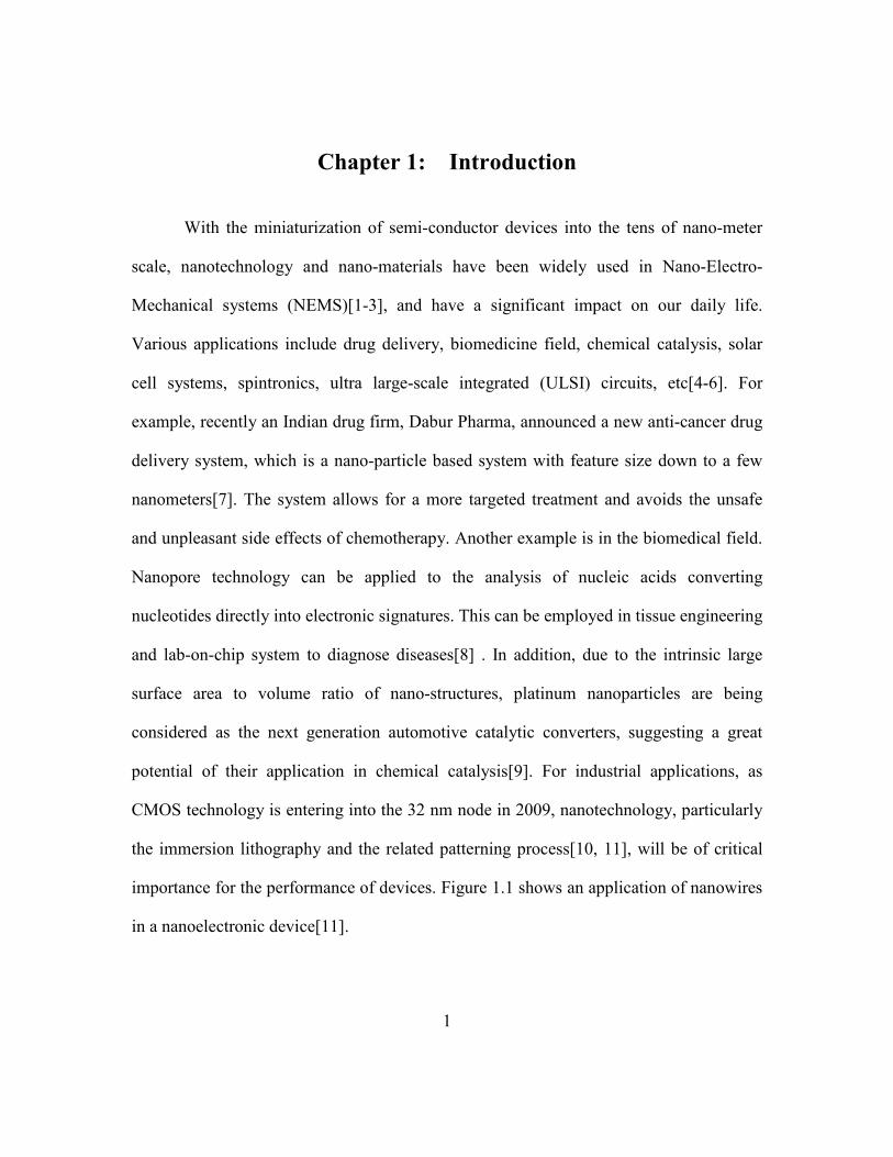
importance for the performance of devices. Figure 1.1 shows an application of nanowires
in a nanoelectronic device[11].
2
Figure 1.1 Application of silicon nanowires in a dual-gate NWFET with Silicided contact [11].
Silicon-based nanostructures are essential building blocks for nanoelectronic
devices and NEMS[1-3]. During operation of nano-devices, the nano-structures are
always subjected to external forces, which can enable or degrade the function of the
devices. Hence, the mechanical properties of the nanostructures play an important role in
controlling the functionality and reliability of the nano-devices [12-15]. However,
mechanical characterization at nanoscale remains challenging for properties such as yield
strength, fracture strength, contact and friction properties, which are often distinctly
different at the nanoscale from their bulk properties. Thus, the investigation of the
material properties of silicon-based structures at the nano-metric scale is important for
both scientific understanding and practical applications.
Fabrication and the corresponding characterization metrologies of the silicon-
based nano-structures are of great challenge[16]. The effort to understand the behavior of
highly constrained materials (size effect) at the nanoscale has gained a lot of interests
3
recently, particularly for feature sizes in the range of tens of nanometer[17]. In order to
investigate mechanical properties of nano-structures, fabrication of well-controlled nano-
structures is one of the major fields of the current research work. For mechanical
characterization, Nanomechanic experiments are devoted to studying fundamental
mechanical properties of physical systems at the nanoscale, such as the strain to failure,
friction properties, etc[18, 19].
In this thesis work, the scaling effect on mechanical and physical properties of
silicon nanolines (SiNLs) will be investigated. The mechanical responses, especially the
buckling behavior and nanofriction of SiNLs[17, 20], were studied by a nanoindentation
technology. For this study, we have developed an E-beam lithography and anisotropic
etching process that enabled us to produce SiNLs with a width as small as 25nm and with
vertical sidewalls almost atomically smooth. Using these structures, we are able to study
the deformation behavior of SiNLs and to measure the contact friction as a function of
materials and nanoscale dimensions. The results from this study revealed distinct
deformation behavior including an elastic range approaching the theoretical limit of Si
crystals and interesting buckling behaviors under nano-indentation. The thesis includes
three major parts: a). fabrication process developed for the formation of well-controlled
SiNLs; b). characterization of mechanical properties of silicon nanolines (SiNLs) based
on the buckling behavior; and c). the nanofriction of the SiNLs.
In this introductory chapter, we will discuss the challenges of fabricating and
characterizing nano-structures, objectives and a literature survey on contact mechanics
and friction at the nano-scale, respectively. This chapter concludes with an overview of
the dissertation.
4
1.1 Challenges of Fabrication and Characterization of Nano-structures
In order to investigate the mechanical and electrical properties of nano-structures,
it is necessary to fabricate good quality nanostructures with controlled microstructure and
geometry. Fabrication of well-controlled silicon-based nanostructures is a significant
challenge[17, 19, 21, 22]. Generally, there are two approaches to creating small scale
nano-structures: bottom-up or top-down.
The first approach employs a bottom-up synthesis method, in which single
crystalline nano-structures are formed through two fundamental steps: nucleation and
growth by well-defined chemical or physical synthesis processes. For example, in the
past decade, a vapor-liquid-solid (VLS)[21] process and metal-catalyzed chemical vapor
deposition (MCCVD)[23] were successfully developed to grow single crystalline silicon
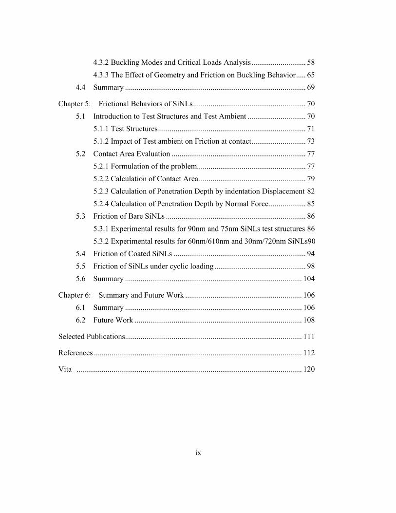
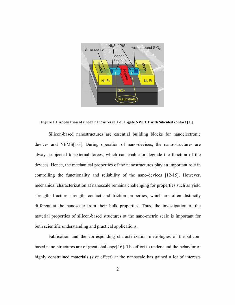
nanowires with a diameter of ~ 10-100 nm[24]. Figure 1.2 shows two scanning electron
microscope (SEM) images of SiNWs grown by the bottom-up approach. The feature size
of the obtained nanowires can be as small as 10 nm, which was not restricted by the
resolution of conventional lithography tools. However, it was difficult to precisely
control the nanowire dimensions, and to form test structures with proper orientations by
this fabrication process. Moreover, the placement of the nanowires for measurements can
be very challenging.
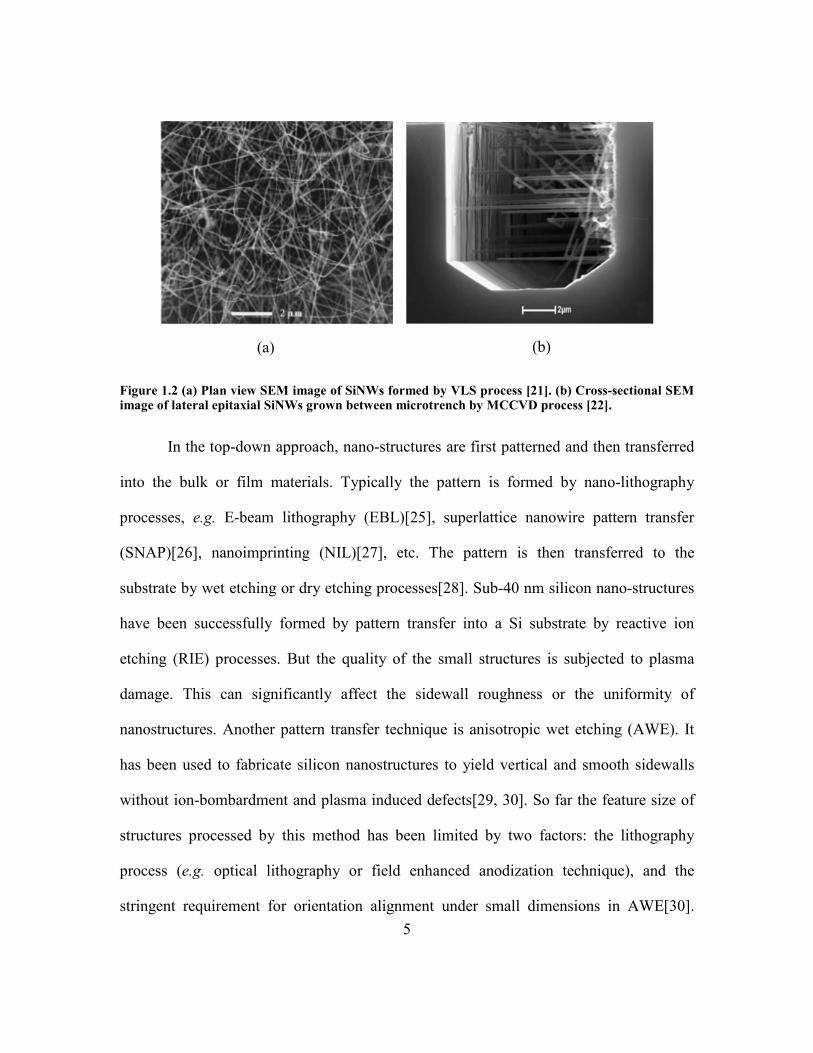
5
Figure 1.2 (a) Plan view SEM image of SiNWs formed by VLS process [21]. (b) Cross-sectional SEM image of lateral epitaxial SiNWs grown between microtrench by MCCVD process [22].
In the top-down approach, nano-structures are first patterned and then transferred
into the bulk or film materials. Typically the pattern is formed by nano-lithography
processes, e.g. E-beam lithography (EBL)[25], superlattice nanowire pattern transfer
(SNAP)[26], nanoimprinting (NIL)[27], etc. The pattern is then transferred to the
substrate by wet etching or dry etching processes[28]. Sub-40 nm silicon nano-structures
have been successfully formed by pattern transfer into a Si substrate by reactive ion
etching (RIE) processes. But the quality of the small structures is subjected to plasma
damage. This can significantly affect the sidewall roughness or the uniformity of
nanostructures. Another pattern transfer technique is anisotropic wet etching (AWE). It
has been used to fabricate silicon nanostructures to yield vertical and smooth sidewalls
without ion-bombardment and plasma induced defects[29, 30]. So far the feature size of
structures processed by this method has been limited by two factors: the lithography
process (e.g. optical lithography or field enhanced anodization technique), and the
stringent requirement for orientation alignment under small dimensions in AWE[30].
(b) (a)
6
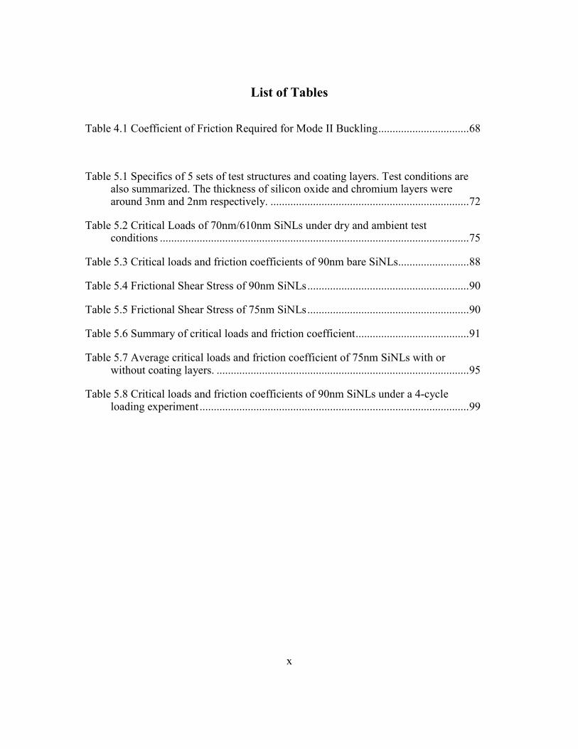
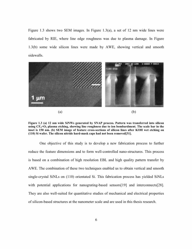
Figure 1.3 shows two SEM images. In Figure 1.3(a), a set of 12 nm wide lines were
fabricated by RIE, where line edge roughness was due to plasma damage. In Figure
1.3(b) some wide silicon lines were made by AWE, showing vertical and smooth
sidewalls.
Figure 1.3 (a) 12 nm wide SiNWs generated by SNAP process. Pattern was transferred into silicon using CF4+O2 plasma etching, showing line roughness due to ion bombardment. The scale bar in the inset is 150 nm. (b) SEM image of feature cross-sections of silicon lines after KOH wet etching on (110) Si wafer. The silicon nitride hard-mask caps had not been removed[31].
One objective of this study is to develop a new fabrication process to further
reduce the feature dimensions and to form well-controlled nano-structures. This process
is based on a combination of high resolution EBL and high quality pattern transfer by
AWE. The combination of these two techniques enabled us to obtain vertical and smooth
single-crystal SiNLs on (110) orientated Si. This fabrication process has yielded SiNLs
with potential applications for nanograting-based sensors[19] and interconnects[28].
They are also well-suited for quantitative studies of mechanical and electrical properties
of silicon-based structures at the nanometer scale and are used in this thesis research.
(a) (b)
7
1.2 Mechanical Characterization of Nano-structures
The scaling effect on mechanical properties is readily observed and is generally
attributed to a change in the properties due to the small dimension of internal structure or
in the overall sample size. Well-known examples are the improvement of the yield
strength of metallic alloys through refinement of the grain size[32] and fine whiskers. For
nano-structures, with dimension approaching micro- or nano-meter ranges, the sample
size is expected to become an important factor for controlling their mechanical strength.
Previously, single-crystal silicon (Si) beams with widths from 200 nm to 800 nm have
been fabricated by field-enhanced anodization using an atomic force microscope (AFM)
[33, 34]. Mechanical characterization of these Si beams by AFM bending tests showed a
strong size effect on bending strength, which was defined to be the maximum tensile
stress in a specimen subjected to bending up to fracture, but no size effect on Young’s
modulus was observed. The reported bending strength was in the range of 11 GPa to 18
GPa, significantly higher than the average strengths for microscale Si beams (4 GPa) and
millimeter scale Si beams (around 500 MPa)[33].
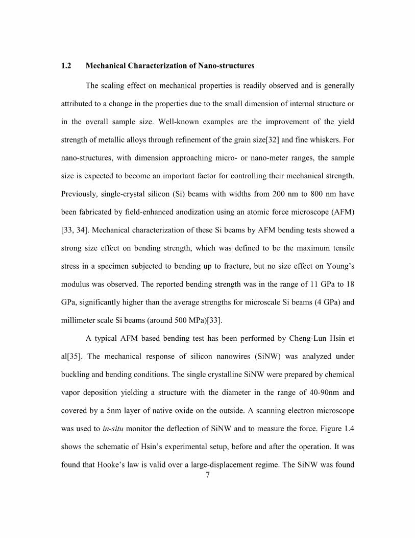
A typical AFM based bending test has been performed by Cheng-Lun Hsin et
al[35]. The mechanical response of silicon nanowires (SiNW) was analyzed under
buckling and bending conditions. The single crystalline SiNW were prepared by chemical
vapor deposition yielding a structure with the diameter in the range of 40-90nm and
covered by a 5nm layer of native oxide on the outside. A scanning electron microscope
was used to in-situ monitor the deflection of SiNW and to measure the force. Figure 1.4
shows the schematic of Hsin’s experimental setup, before and after the operation. It was
found that Hooke’s law is valid over a large-displacement regime. The SiNW was found
8
to be able to sustain a critical strain of 1.5%, which was much larger than the 0.2%-0.5%
of its bulk. The elastic modulus of the NW was determined to be 175–200 GPa, based on
analysis of the force vs. displacement curves. The study indicates the superior mechanical
properties of SiNWs, including the ultrahigh flexibility and the toughness.
Figure 1.4 Schematic of experiments setup, a) before and b) after the manipulation[35].
In addition to the AFM bending tests, nanoindentation is a commonly used
technique for material characterization of nano-structures. The nanoindentation technique
is well established for measurements of elastic modulus, hardness, and fracture toughness
of both bulk and thin film materials[36, 37]. The precision in both force and displacement
measurements, together with easy sample preparation, have led to recent applications of
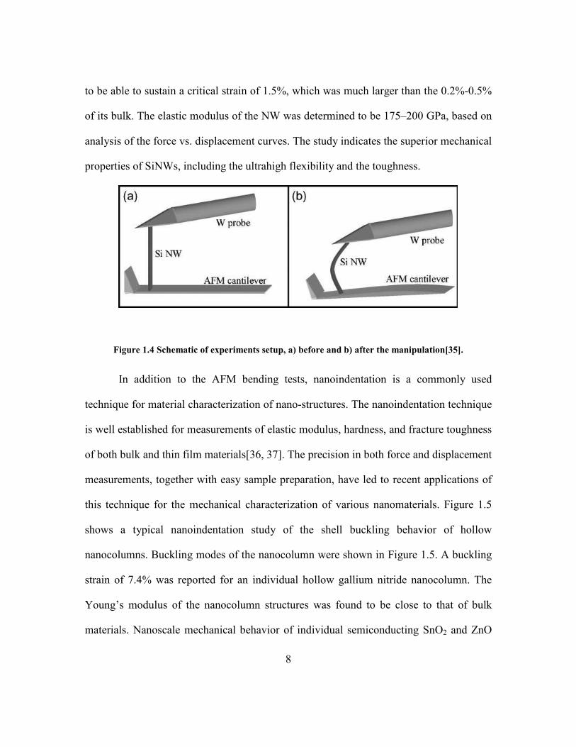
this technique for the mechanical characterization of various nanomaterials. Figure 1.5
shows a typical nanoindentation study of the shell buckling behavior of hollow
nanocolumns. Buckling modes of the nanocolumn were shown in Figure 1.5. A buckling
strain of 7.4% was reported for an individual hollow gallium nitride nanocolumn. The
Young’s modulus of the nanocolumn structures was found to be close to that of bulk
materials. Nanoscale mechanical behavior of individual semiconducting SnO2 and ZnO
9
nanobelts have also been investigated by Mao et. al. [18]. The nanobelt is a quasi one-
dimensional solid nanostructure with rectangular cross-section. This study shows the
feasibility of nanoindentation technique on the study of patterned one-dimensional
structures. For the nanoindentation studies, interpretation and analysis of the result is
nontrivial and often requires sophisticated modeling[38, 39].
Figure 1.5 Schematic of nanoindentation experiments on hollow column at deferent stages of the indentation process and different possible buckling modes[40].
In this thesis, the nanoindentation technique and numerical simulations by finite
element methods (FEM) are employed to characterize the buckling behavior of the
SiNLs. We will report results on elastic modulus, strain to fracture and contact friction
properties for SiNLs.
1.3 Nanofriction of SiNLs
Owing to the large surface to volume ratio, friction at contact is of fundamental
importance for reliability of micro/nano systems, such as NEMS devices and high-density
hard-disk drives[2, 4]. A transition of frictional shear strength has been reported, showing
a decrease of about one order of magnitude as the contact radius shrank into the
nanoscale range[41]. This indicated a size effect on the contact friction properties.
10
Friction of nanostructures is of great importance for various nano-devices.
Generally, the scale of the device and the very large surface-area-to-volume ratio at the
nanometer scale influences the friction and adhesion properties at the contact[41, 42].
The degradation of such properties can cause serious performance and reliability
problems for nano-devices. Therefore, there is an inherent need to understand the friction
phenomenon at nanoscales.
There are two major theories of friction, the classical Amontons and
Coulomb’s[43] laws of friction and the Bowden-Tabor Theory[44]. The classical
Amontons and Coulomb’s laws of friction can be expressed as
NF µ= . (1. 1)
These laws can be summarized as
1. The force of friction is directly proportional to the applied normal load
(Amontons 1st law); the coefficient is called the friction coefficient;
2. The force of friction is independent of the apparent area of contact (Amontons 2nd
law);
3. The friction is independent of the sliding velocity (Coulomb’s law).
These three laws have been verified by empirical observations for many years and
are still being applied to many engineering problems today. However, there are examples
where these laws do not apply. One example is that geckos are able to climb up vertical
surfaces[45]. This fact apparently contradicts Coulomb’s laws, where the nominal normal
force is zero therefore the frictional force should be zero. This suggests that other
mechanisms such as adhesion have to be taken into consideration in the study of
mechanical behavior of contacts. The application of nano-devices requires an
11
understanding of the friction and contact behavior at the micro- and nanoscale.
Recent studies show that stronger adhesion will result in a larger friction force.
New theories that include the frictional adhesion were developed accordingly[42, 45-58].
Bowden and Tabor, based on their work with metal-on-metal sliding, proposed that the
friction force can be expressed as:
AF τ= , (1. 2)
where τ is the frictional shear strength and A is the true contact area. This theory is based
on a purely elastic sliding process and the Hertzian contact theory. The true contact area
is taken to be a continuum representation of the number of atoms involved in the
adhesive or cohesive interactions between two sliding surfaces. Explicitly, the frictional
force and the frictional shear stress are independent of the applied load in this theory.
However, according to the elasticity theory, the applied load plays an important role in
determining the true contact area A. In addition, results from molecular dynamics
simulations suggested that frictional shear stress τ is weakly depends on the normal
pressure[59, 60]. It was also found that under the condition of the true contact area
linearly depending on the applied normal load, the classical Coulomb laws and the
Bowden-Tabor theory become the same. In this case, the Bowden-Tabor theory offers a
completely different understanding of the fundamental mechanisms of friction and
contact mechanics.
The complexity of the Bowden-Tabor theory originates in the fact that the friction
coefficient is not an intrinsic physical property. Particularly, at a nano-scale the variation
of contact area is determined by local contact details. The friction coefficient and
frictional shear stress/contact area in general depend on the specific structure, chemistry
12
and elastic properties of contacting surfaces, the test environment and conditions, and the
contact history.
Because of the complexity to evaluate the frication behavior, it is necessary to
design and conduct experiments on well-defined interfaces, especially for investigation at
nano-scale. One widely used metrology is the application of a single-asperity contact
model, i.e. the contact measurement of a probe tip and a flat surface by the scanning
probe microscope (SPM). With a well-defined geometry, the SiNLs is a good candidate
for the study of contact measurements. The associated contact mechanics will be
discussed in Chapter 2. The general models of contact mechanics are based on the
Hertzian contact theory. The details of the contact area evaluation as well as the nano-
friction study will be discussed in Chapter 5, with the assumption of a single-asperity
model.
1.4 Objective and Organization of Dissertation
The purpose of the present work is to study the mechanical response and friction
behavior of the Silicon Nanolines (SiNLs) structures by a nanoindentation technique,
based on the analysis of the buckling behaviors of SiNLs. The friction coefficients were
evaluated based on the classical Amontons using Coulomb’s laws of frictions and Finite
Element Simulation. For comparison, frictional shear stresses in the Bowden-Tabor
theory will be calculated. The area of contacting surfaces between a diamond indenter
and SiNLs structures will be evaluated based on the Hertzian contact theory. The impact
of contact history on the frictional behavior of SiNLs will be studied by a set of cyclic-
loading nanoindentation experiments.
13
Following this introductory chapter, Chapter 2 will review in the theoretical
background of the buckling behaviors of column structures and contact mechanics
between a sphere and a flat half-space. In Chapter 3, the experimental techniques,
including the fabrication methods developed to fabricate SiNLs test structures and the
nanoindentation technique, will be presented. In Chapter 4, the mechanical response of
SiNLs under nanoindentation will be described. The loading-displacement indentation
curves show that the critical load to induce the buckling of the SiNLs can be correlated to
the contact friction of the nano-indenter and the geometry of SiNLs. The mapping of
buckling mode selection with the geometry, applied load and friction is developed.
Chapter 5 will begin with details of contact area calculations for the SiNLs geometry,
which is followed by discussion of the results from experiments and nanofriction model
analysis. Finally, in Chapter 6 we will present a summary of the dissertation and some
suggestions for future work.
14
Chapter 2: Contact Mechanics and Compressive Instability
of Columns
In this chapter, the first section is an introduction to the contact mechanics for a
single asperity contact. Then, it is followed by a discussion about the buckling behavior
of column structures.
In the nanoindentation experiment, the contact between the nanoindenter and
SiNLs can be approximated as a single asperity contact. In order to evaluate the frictional
shear stress, the true contact area has to be determined. In some cases, the contact area
can be determined by experimental techniques. For example, with a surface force
apparatus (SFA), the contact area can be directly evaluated by interference fringes[61,
62]; and if both materials in contact are electrically conductive, the contact area can be
estimated by the variation of electrical current passing through the contact zone[63, 64].
However in AFM or MFT, it is impossible to directly measure the contact area, several
methods and models have been developed to evaluate the contact area indirectly[65-67].
These methods and models are based on contact mechanics theories, and the
corresponding results are consistent with the experimental data. In the first section,
classical contact mechanics will be reviewed; then, contact mechanics theories that
include adhesion between contacting surfaces will be discussed.
In the nanoindentation experiments, the indenter imposed vertical forces on
SiNLs and a sudden displacement burst was observed during the loading and unloading
cycle. Such a displacement burst was characterized as buckling behavior of SiNLs. When
15
a column structure is subjected to compressive forces, buckling may occur [65]. Buckling
is a failure mode where a strut, rod, plate, or column reaches an unstable state under
compressive stress and laterally deflects. In the second section of this chapter, SiNL
structures were modeled as a column structure with one end fixed and the other end free
or pinned. The buckling behaviors of column under such boundary conditions will be
analyzed in Section 2.2.
2.1 Contact Mechanics of a Sphere pressed into a Half-space
It is complicated to evaluate the contact areas between surfaces of arbitrary
profiles. One of the simplest models is the classical Hertzian contact model between a
sphere and half-space. In the Hertzian model, the mating parts are assumed to be elastic
and have no adhesive force attraction[66]. When adhesion is considered, the classical
Hertzian model has to be modified. The DMT[67], JKR[68], and Maugis[69] models
include the effect of adhesive attraction, and cover a wide range of the adhesion spectrum.
In this thesis work, the feature sizes of the test structures, SiNLs, scale down to
30nm and into the regime of nano-contact where the adhesion may play an important role
in the nano-devices and nano-materials. Although eventually we will find out that the
adhesion is not the key factor to determine buckling behavior of SiNLs, several classic
contact mechanics, the Hertzian model, DMT, JKR, and Maugis models, will be
reviewed here to give a whole background of the contact mechanics.
2.1.l Adhesionless Contact Mechanics - Hertzian Model[66]
The geometry of the Hertzian model is shown in Figure 2.1 a) before contact is
16
made. The spherical punch has a radius of R, which is pressed into the half-space. It is
assumed that the punch is rigid, and the half-space is elastic. In reality, the punch and the
half-space both possess finite modulus, which can be modeled that the punch is rigid but
the half-space has a reduced modulus of,
2
22
1
21 111
EEEr
νν −+
−= ,
where E1 and E2 are the Young’s modulus of the punch and half-space, and ν1 and ν2 are
their Poisson ratio, respectively. When the contact zone is small compared to the size of
the punch, the shape profile of the punch can be approximated as
R
rrf
2)(
2
= ,
where r is the lateral distance measured from the apex of the punch. When the punch is
pushed a distance ∆ into the half-space, a contact zone of circular shape with radius a will
form. ∆ is also called penetration depth. The relation between ∆ and a is
Ra 2
=∆ .
The stress distribution inside the contact zone was demonstrated by Hertz to be,
2/12
2
0 )1(ar
pp −= ,
where p0 is the maximum stress at the center of the contact zone. The total force is
calculated by integrating the stress p over the contact area, and found to be
RaE
aF rH 3
4)(
3
= .
Therefore, once given the material properties of the interacting objects and the
17
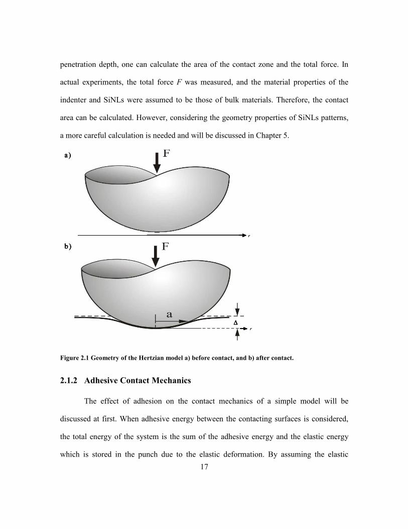
penetration depth, one can calculate the area of the contact zone and the total force. In
actual experiments, the total force F was measured, and the material properties of the
indenter and SiNLs were assumed to be those of bulk materials. Therefore, the contact
area can be calculated. However, considering the geometry properties of SiNLs patterns,
a more careful calculation is needed and will be discussed in Chapter 5.
Figure 2.1 Geometry of the Hertzian model a) before contact, and b) after contact.
2.1.2 Adhesive Contact Mechanics
The effect of adhesion on the contact mechanics of a simple model will be
discussed at first. When adhesive energy between the contacting surfaces is considered,
the total energy of the system is the sum of the adhesive energy and the elastic energy
which is stored in the punch due to the elastic deformation. By assuming the elastic
a)
b)
∆∆∆∆
r
r
a)
b)
∆∆∆∆
a)a)
b)
∆∆∆∆
b)b)
∆∆∆∆
r
r
18
energy only exists inside the contact zone, and denoting the elastic energy as εH(∆) and
the adhesive energy per unit area as ω, the total energy would be
AH ωεε +∆=∆ )()( ,
where A is the area of the contact zone. The total force is calculated as
∆+
∆=
∆=
ddA
dd
dd
F H ωεε
.
The first term is the Hertzian force and the second term is the adhesive force, which can
be calculated in this simple model to be -πRϖ. Therefore the effect of adhesion is an
offset of the Hertzian force by a constant -πRϖ.
More complicated models consider the material properties and the nature of
adhesion[45, 56, 70-73]. One famous model is the DMT model developed by Derjaguin
and coworkers. Another famous model called JKR was developed by Johnson et. al. In
these two theories, the contact problem is modeled in two different elastic regimes.
The DMT model assumes that the elastic deformation occurs inside the contact
zone, and the Hertzian stress distribution and penetration fields only apply inside the
contact zone as well. However the adhesive interaction only applies outside of the contact
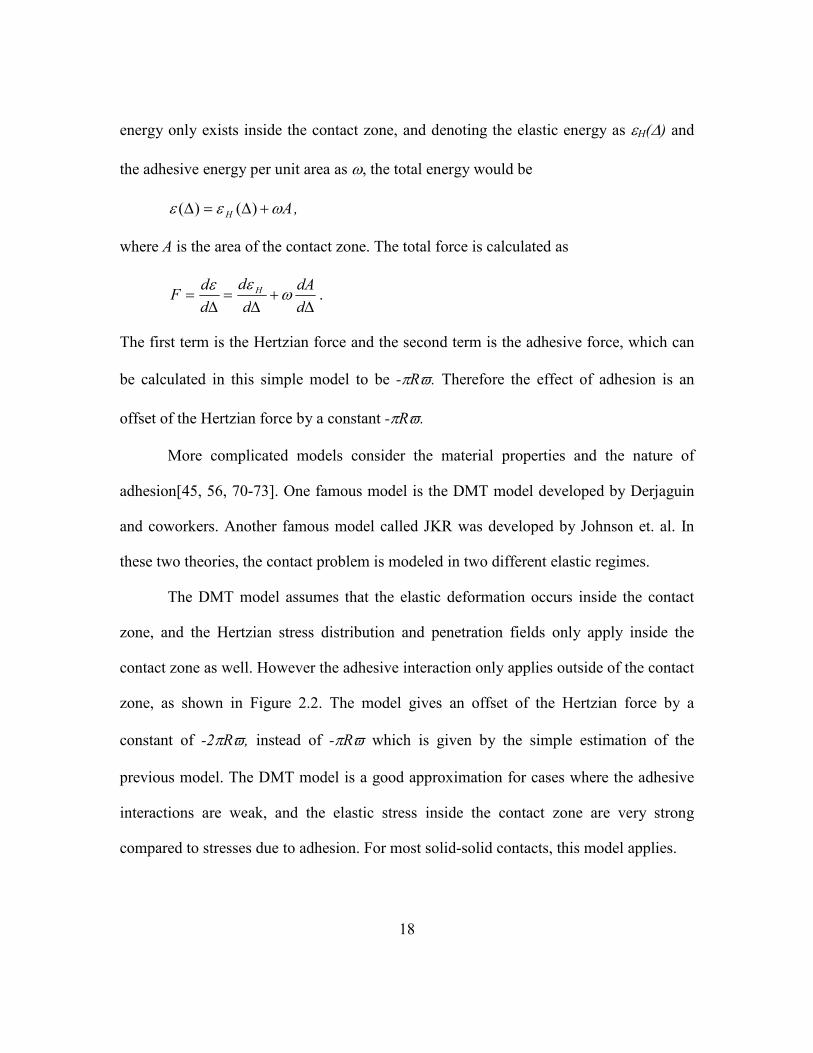
zone, as shown in Figure 2.2. The model gives an offset of the Hertzian force by a
constant of -2πRϖ, instead of -πRϖ which is given by the simple estimation of the
previous model. The DMT model is a good approximation for cases where the adhesive
interactions are weak, and the elastic stress inside the contact zone are very strong
compared to stresses due to adhesion. For most solid-solid contacts, this model applies.
19
Figure 2.2 Geometry of the DMT adhesive contact. The attractive interactions act outside the contact zone.
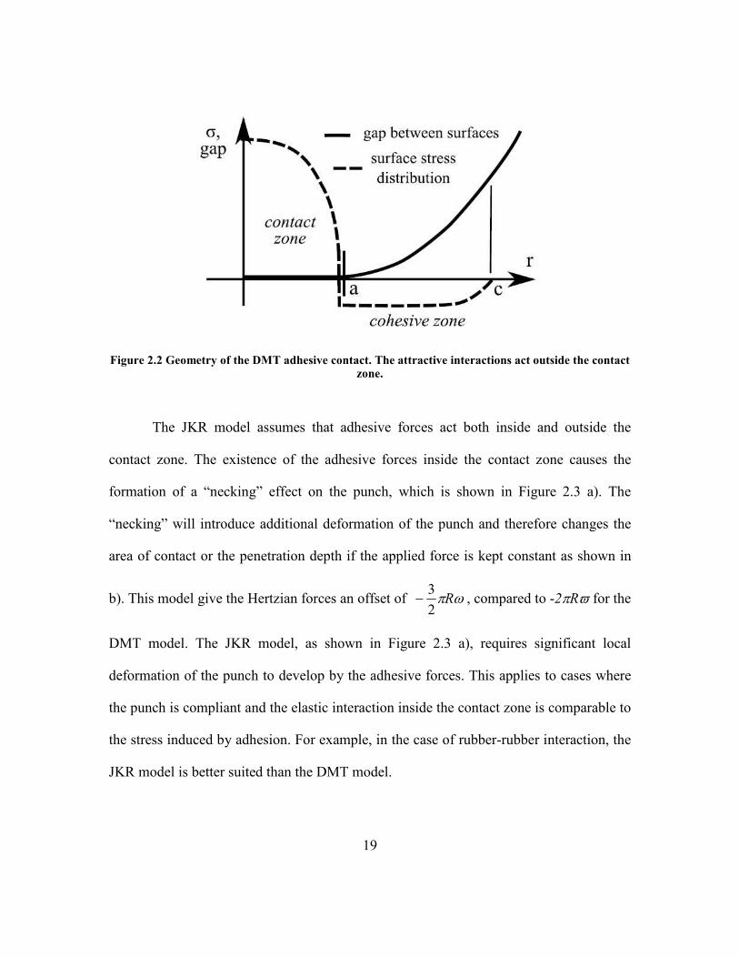
The JKR model assumes that adhesive forces act both inside and outside the
contact zone. The existence of the adhesive forces inside the contact zone causes the
formation of a “necking” effect on the punch, which is shown in Figure 2.3 a). The
“necking” will introduce additional deformation of the punch and therefore changes the
area of contact or the penetration depth if the applied force is kept constant as shown in
b). This model give the Hertzian forces an offset of ωπR23
− , compared to -2πRϖ for the
DMT model. The JKR model, as shown in Figure 2.3 a), requires significant local
deformation of the punch to develop by the adhesive forces. This applies to cases where
the punch is compliant and the elastic interaction inside the contact zone is comparable to
the stress induced by adhesion. For example, in the case of rubber-rubber interaction, the
JKR model is better suited than the DMT model.
20
Figure 2.3 Schematic illustration of JKR adhesive contact. The existing of adhesive forces changes the area of the contact zone which is shown by the formation of “necking” in a) outside of the contact zone denoted by dashed curve. In order to keep the area of contact zone constant under this case, a negative force is need to “pull out” the punch a little which is shown in b).
However, the DMT and JKR models together do not cover all cases. There are
cases where the adhesive interactions are in an intermediate range, and the adhesion
induced deformation is comparable to the punch displacement. The adhesive forces
contribute to the deformation of the punch by an extent that is not fully in the JKR regime.
The interactions have to be considered both inside and outside of the contact zone. One
method is a superposition of JKR and DMT terms for the penetration depth and forces,
21
)()()()(
)()(
aFaFaFaF
aa
DMTJKRH
JKRH
++=
∆+∆=∆,
where ∆JKR is the offset of penetration depth by the JKR model, and FJKR and FDMT are the
offset of forces by JKR and DMT models, respectively. The FJKR and FDMT can not be
simply evaluated by the JKR or DMT model, and elaborate calculations are needed.
Maugis developed a quasi-analytical method that is now generally called the Maugis
model to circumvent the difficulties[69]. The calculation is complicated but, as expected,
this model gives an offset of the Hertzian forces by -nπRϖ, where 1.5<n<2.
For each model, the penetration depth and contact radius can also be calculated if
the adhesive energy is measured or calculated. This gives us the capabilities to calculate
the area of the contact which is important to evaluate frictional shear stresses. It is noted
that these three models cover a large spectrum of adhesive interactions. An important
problem is the selection of an appropriate model under specific experimental condition.
Tabor first defined a non-dimensional parameter[74],
3/130
)16
(z
RT 2Κ9
=ωµ ,
where K is the effective modulus and rEK34
= , z0 is the interatomic equilibrium
distance in a Lennard-Jones potential. This parameter was used to characterize the
adhesion spectrum and determine which model, DMT, JKR, or Maugis, is appropriate.
The Tabor parameter is defined by the ratio of the penetration depth versus the decay
length of the adhesive interactions. The parameter measures the impact of the interaction
stresses on the deformation of the punch. There are some variations of this parameter
22
when the existence of moisture interlayer and capillary forces are considered, however
the selection of models generally falls within the following rule,
model Maugis 51.0
model DMT 1.0
model JKR ,5
<<
<
>
T
T
T
µµµ
.
When the deformation due to adhesion is small and the interaction has long range forces,
the value of the parameter is small, and the DMT model is a good choice. DMT normally
works well for solid-solid interactions with small adhesion and small punch compliance.
On the other hand, if the deformation is large due to adhesion with a short range
interaction force, the JKR model is better.
2.2 Compressive Instability of Columns
In this section, the fundamental of buckling mechanics will be reviewed.
Although all three cases reviewed below are classic cases with simple boundary
conditions, they provide a good starting point to understand the buckling behaviors and
the conditions that determine buckling modes. Specific boundary conditions and more
complicated cases related to the SiNLs nanoindentation experiments will be discussed in
Chapter 4 and Chapter 5.
When an elastic beam or column structure is subjected to a compressive load, the
structure undergoes elastic response. But as the compressive load further increases to
some critical load, the column becomes unable to support the load and reaches an
unstable state[65, 75]. At the critical load, any other transverse force, no matter how
small it is, can cause the deflection of the structure to mathematically reach infinity. Such
23
an elastic instability under a compressive load is called buckling. There are several other
common types of elastic instability such as lateral buckling. Reviewed here is the
compressive instability of beam-column structures, which will be applied to simulate the
SiNLs structures in Chapter 4.
The basic differential equation of a beam-column deformation is
Qdz
xdF
dzxd
EI =+2
2
4
4
, (2.2.1)
where x(z) is the deflection of the beam-column at any position z, E is the Young’s
Modulus and I is the second moment of inertia of the beam’s cross section, Q(x) is the
transverse load acting on the beam, and F is the applied load. When Q(x) is negligible,
the beam-column structure becomes a column structure.
Three common cases are considered as shown in Figure 2.4. Case one, both ends
of the beam-column are fixed, for which the boundary conditions are
0)(')()0(')0( ==== hxhxxx (2.2.2)
where x(0)=0 indicates that the deflection is zero, and x’(0)=0 indicates that the slope is
zero.
Case two, one end (z=0) is fixed, and the other end (z=h) is hinged and allowed to
rotate. The corresponding boundary conditions are
0)(")()0(')0( ==== hxhxxx (2.2.3)
where x”(h)=0 indicates the moment at the end is zero.
Case three, both ends of the beam-column are hinged and allowed to rotate. The
boundary conditions are
0)(")()0(")0( ==== hxhxxx (2.2.4)
24
The general solution of equation 2.2.1 is
2
2sincos)( z
FQ
DCzkzBkzAzx ++++= ,
where k satisfies EIF
k =2 .
Considering the boundary conditions of Case one as expressed in equation 2.2.2,
the solution for the deflection of the beam gives
kFQ
kzhkh
kzhkzhzzx2
)sin)2
cot()1(cos)(()( +−+−= .
As mentioned previously, at the critical load, the deflection of the beam reaches
infinite mathematically, which indicates that ∞=)2
cot(kh
, and kh satisfies kh=2nπ with
n=1, 2, 3…. Recall that k is defined as EIF
k =2 , and the critical load is determined by
setting n=1, therefore the buckling occurs at 2
24h
EIFcr
π= .
Similarly, Case two gives the solution of deflection,
FkQ
khkhkhkzkhkzzhkhkkhzhkkhhkzhkzzhk
zx 2
222222
2sincoscos2sin2)(sin)2(sin)(cos))(2()(2
)(−
−+−++−−−++−=
and the critical load can be found by solving 0sincos =− khkhkh , that is tankh=kh
which can be solved numerically to be kh=4.493, and critical load 2
2493.4h
EIFcr = .
25
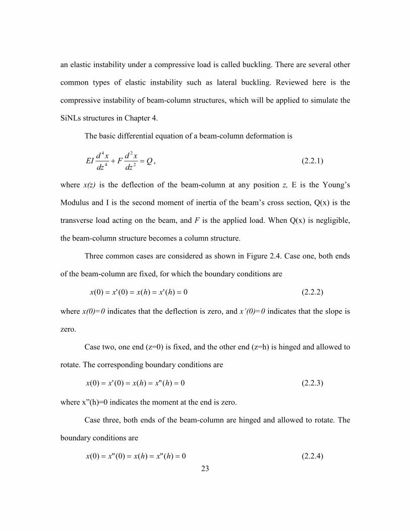
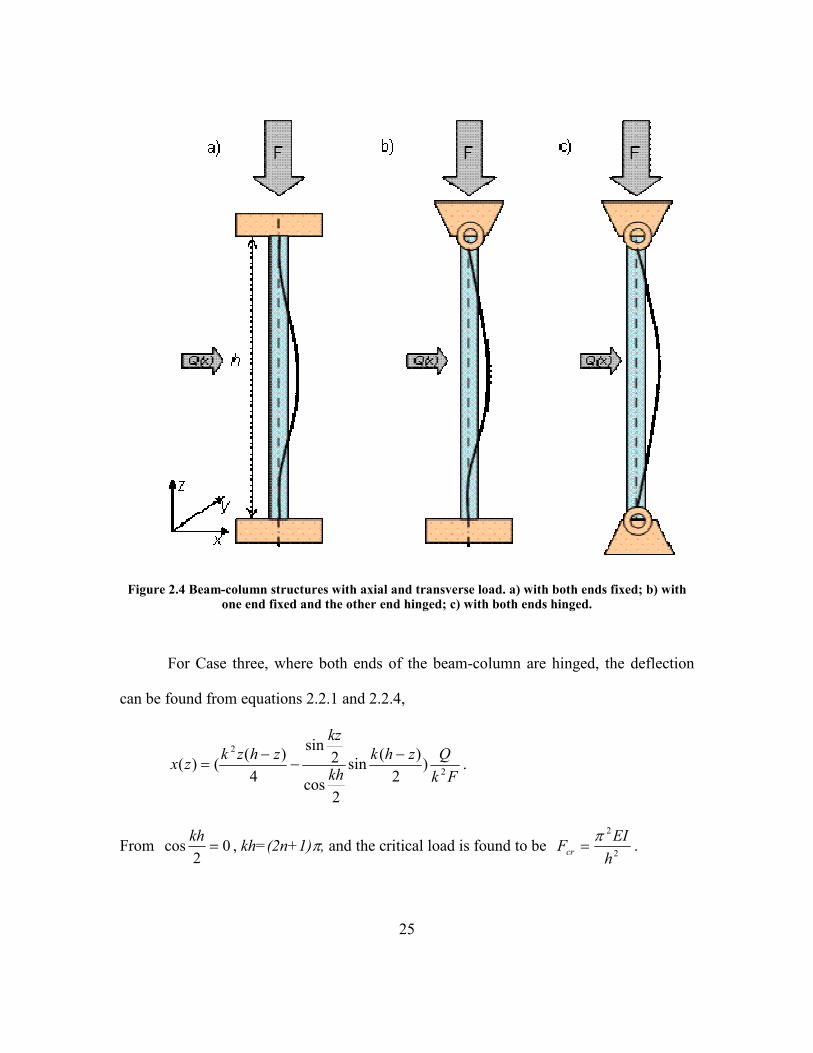
Figure 2.4 Beam-column structures with axial and transverse load. a) with both ends fixed; b) with one end fixed and the other end hinged; c) with both ends hinged.
For Case three, where both ends of the beam-column are hinged, the deflection
can be found from equations 2.2.1 and 2.2.4,
Fk
Qzhkkh
kzzhzk
zx2
2
)2
)(sin
2cos
2sin
4)(
()(−
−−
= .
From 02
cos =kh
, kh=(2n+1)π, and the critical load is found to be 2
2
hEI
Fcr
π= .

26
In the experiments, SiNLs was simulated as a column structure with the bottom
end fixed but the top end hinged or free, depending on the buckling modes. When the top
end is free, the analysis is analogous to Case three with its height being assigned in half.
More details on the buckling behaviors of SiNLs will be presented in Chapter 4. The
solution of buckling response under eccentric loading condition will also be discussed in
Chapter 4.
27
Chapter 3: Experimental Techniques
In this chapter, a fabrication process was developed to prepare nanoindentation
test structures. The SiNL test structures were fabricated on a single crystalline [110]
silicon wafer. To achieve test structures with well-controlled micro-structure and
geometry at nanoscale, anisotropic wet etching (AWE) was employed for pattern
formation. Other major fabrication techniques involved were electron-beam lithography,
reactive plasma etching, and chemical etching. Generally, patterns were formed by the
electron-beam lithography (EBL). EBL has the capability to generate patterns with
feature sizes down to tens of nanometers. Then patterns are transferred into the silicon
substrate by selective etching process, i. e. reactive ion etching (RIE) or AWE.
3.1 Fabrication of SiNL Test Structures
For mechanical characterization at nano-scale, it is of critical importance to form
well-control test structures, i.e. uniform feature size, smooth sidewalls, etc. In this
section, the fabrication process to obtain single crystalline silicon nano-line structures,
having nearly atomic flat sidewalls and uniform linewidths, will be introduced. The
general fabrication process flow will be briefly reviewed, followed by a detailed
introduction to some key process steps and challenges. The quality of the fabricated
SiNLs will be discussed, based on SEM images of them.
The fabrication process began with a chromium coating by an e-beam evaporator
on (110) silicon wafers already having an oxide layer deposited on their upper surfaces
by low pressure chemical vapor deposition (LPCVD). After chromium evaporation, a
28
positive-tone resist was spun on the wafer. The resist was imaged on an electron-beam
exposure system operating at 50 kV. Pattern transfer from the resist to chromium lines
was performed by reactive plasma etching (RIE) through the oxide layer down to the
silicon surface using the chromium lines as the etch mask. Subsequently, the residual
resist was removed and tetra-methyl-ammonium hydroxide (TMAH) was used for
anisotropic wet etching (AWE) of silicon along the (111) planes. Finally, chromium and
oxide hard masks were removed by chromium etchant and buffered oxide etchant dip.
In Section 3.1.1 the EBL process will be introduced. The RIE and some details of
the associated pattern transfer will be further introduced in section 3.1.2. The AWE
technique, which is the critical process for pattern transferring into silicon wafers, will be
discussed in detail on section 3.1.3. Section 3.1.4 is about the integration of the
fabrication process and the corresponding challenges.
3.1.1 Electron Beam Lithography Technique
Electron beam lithography (EBL) is one of the premier techniques for defining
structures with nanometer dimensions [76]. The electron beam has much shorter
wavelength compared with that of the conventional optical lithography techniques, which
gives the capability to overcome the diffraction limit of light. The electron beam also
changes the properties of the resist, which makes the resist either more soluble or less
soluble after the resist is exposed to the electron beam. Positive resist will be more
soluble after being subjected to electron beam exposure and the exposed materials will be
removed by the developer. While negative resist will be less soluble after electron beam
exposure and the un-exposed materials will be removed.
29
There are a few advantages of using EBL technique in the study. First, EBL
provides the flexibility of a design change and does not require a mask like a
conventional optical lithography. Second, much better dimension resolution is achievable
by EBL, which enables nano-structures to be fabricated with feature sizes as small as 20
nm. EBL writing is a serial process that requires much longer writing time than
conventional optical lithography, but it is not a significant issue in the experiments, since
massive productivity is not an important issue in a laboratory research. EBL writing is
widely used in the industry for mask writing due to its flexibility of design change.
In the EBL exposure, the selection of wafer stack is important. A typical layer
stack for the experiments is shown in Figure 3.1. First, a piece of silicon wafer was
prepared with a 15nm thick of chromium deposited on top of a 25nm thick layer of SiO2.
Then, a positive EBL resist layer was spin-coated on top. The thickness of the EBL resist
was around 145nm. The purpose of a SiO2 layer was to serve as a hard mask for the
pattern transfer, and prevent formation of silicide layer between chromium and silicon.
The chromium layer is conductive and was used to change the charging nature of the
substrate during EBL exposure. Without a conductive layer, an insulating substrate
surface will charge up during an EBL exposure and may cause the distortion of the
patterns. Even on semiconductor substrate, the conductive layer will help distribute
electron charging. Another advantage of the chromium layer is the high selectivity during
the pattern transfer where a chromium layer serves as a hard mask layer to transfer
patterns into oxide layer.
30
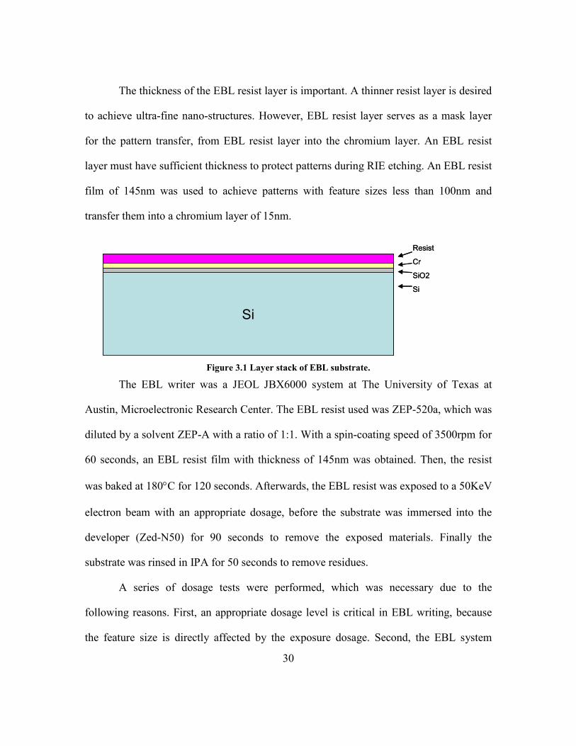
The thickness of the EBL resist layer is important. A thinner resist layer is desired
to achieve ultra-fine nano-structures. However, EBL resist layer serves as a mask layer
for the pattern transfer, from EBL resist layer into the chromium layer. An EBL resist
layer must have sufficient thickness to protect patterns during RIE etching. An EBL resist
film of 145nm was used to achieve patterns with feature sizes less than 100nm and
transfer them into a chromium layer of 15nm.
Figure 3.1 Layer stack of EBL substrate.
The EBL writer was a JEOL JBX6000 system at The University of Texas at
Austin, Microelectronic Research Center. The EBL resist used was ZEP-520a, which was
diluted by a solvent ZEP-A with a ratio of 1:1. With a spin-coating speed of 3500rpm for
60 seconds, an EBL resist film with thickness of 145nm was obtained. Then, the resist
was baked at 180°C for 120 seconds. Afterwards, the EBL resist was exposed to a 50KeV
electron beam with an appropriate dosage, before the substrate was immersed into the
developer (Zed-N50) for 90 seconds to remove the exposed materials. Finally the
substrate was rinsed in IPA for 50 seconds to remove residues.
A series of dosage tests were performed, which was necessary due to the
following reasons. First, an appropriate dosage level is critical in EBL writing, because
the feature size is directly affected by the exposure dosage. Second, the EBL system
Si
Resist
Cr
SiO2
Si
SiSi
Resist
Cr
SiO2
Si
31
condition may change after a period of time. Third, the required dosage level may be
different to achieve the same patterns if the substrate is changed. For example, the
thickness difference in the conductive layer (chromium in the current experiments) may
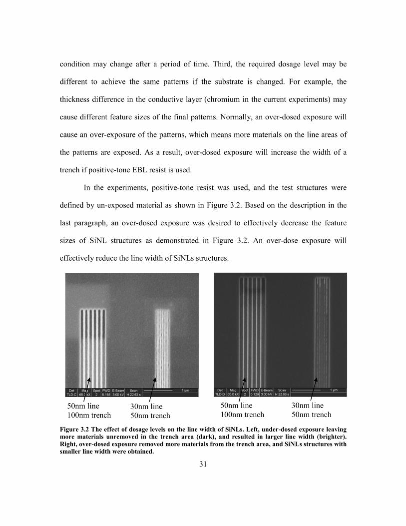
cause different feature sizes of the final patterns. Normally, an over-dosed exposure will
cause an over-exposure of the patterns, which means more materials on the line areas of
the patterns are exposed. As a result, over-dosed exposure will increase the width of a
trench if positive-tone EBL resist is used.
In the experiments, positive-tone resist was used, and the test structures were
defined by un-exposed material as shown in Figure 3.2. Based on the description in the
last paragraph, an over-dosed exposure was desired to effectively decrease the feature
sizes of SiNL structures as demonstrated in Figure 3.2. An over-dose exposure will
effectively reduce the line width of SiNLs structures.
Figure 3.2 The effect of dosage levels on the line width of SiNLs. Left, under-dosed exposure leaving more materials unremoved in the trench area (dark), and resulted in larger line width (brighter). Right, over-dosed exposure removed more materials from the trench area, and SiNLs structures with smaller line width were obtained.
50nm line 100nm trench (a)
30nm line 50nm trench (a)
50nm line 100nm trench (a)
30nm line 50nm trench (a)
32
3.1.2 RIE and Pattern Transfer Process
After EBL exposure and subsequent developing processes, the designed patterns
were formed on the resist layer. The next task was to transfer patterns into the layers
below the EBL resist in the stack on silicon substrate. The patterns were first transferred
into the chromium layer then into the silicon dioxide layer, as shown in Figure 3.1. The
pattern transfer was done by two steps of reactive ion etching (RIE), and then followed
by anisotropic wet etching (AWE). The RIE process is further discussed below, and the
AWE process in section 3.1.3.
RIE is a common technique in the semiconductor industry and research labs.
Neutral or charged particles are generated by plasma in the RIE chamber [77]. Particles
that bombard with the substrate will either chemically react with the substrate materials
or physically liberate the substrate atoms. Typical reaction gases to generate a plasma
include oxygen, fluorine-based gases (such as CF4 or CHF3), and chlorine and bromine
based gases (such as Cl2 or HBr). The selection of reaction gases depends on their etching
rate and selectivity, as well as on the feature sizes of the structures and composition of
the substrate materials. Other parameters of importance for the selection of reaction gases
include the power and design of the plasma chamber. All the factors mentioned can have
an effect on developing an etching recipe. For example, O2 plasma is normally chosen for
ashing or cleaning of the organic contaminants since it has good etching rate and
selectivity on polymers.
The etching recipes used in the processes are summarized next. According to the
layer stack of the EBL substrate shown in Figure 3.1, as a first step, the pattern written by
33
EBL was transferred into the chromium layer. The EBL resist served as the etching mask
in this step. A good etching recipe for this step is characterized by an enough etching rate
on chromium, while the etching rate on EBL resist is small enough that the EBL resist
can survive this step. Such a recipe had been developed using the reaction gases of Cl2
and O2 with a flow rate of 9.7sccm and 2.25sccm, respectively. The base pressure was set
to be 80mTorr and the RF power to be 75W. The etching rate for chromium was
15nm/minute, and 50nm/minute for EBL resist. Normally, the thickness of the mask layer
has to ensure a 100% over-etching of the chromium layer; therefore, at least 100nm of
thickness for the EBL resist was required. As mentioned before, the spin-coated EBL
resist thickness was about 145nm. The second etching step was to transfer patterns into
the silicon dioxide layer where chromium layer served as the hard mask. One of two
etching recipes was chosen in this etching step: one recipe with CF4+O2 and the other
recipe with CHF3+O2 reaction gases. Normally, at least 100% over-etching was desired at
this step to make sure there was no oxide residue in the trench area.
3.1.3 Anisotropic Wet Etching (AWE) Process
Wet etching is a simple etching technique where the material dissolves when
immersed into a chemical solution. To generate patterns and structures of interest, an
etching mask is required to selectively etch the material. The mask material must have a
much lower etching rate compared to the material to be etched. Either silicon dioxide or
chromium is a good mask material for the AWE etching of silicon in TMAH solutions.
Some materials, such as silicon, exhibit anisotropic etching properties in certain etchants
[30, 31, 78]. For example, silicon has a different etching rate in different crystalline
34
directions in TMAH and KOH solutions. The etching rate for the silicon (110) plane is
0.532µm/min, while it is only 0.009µm/min for the silicon (111) plane in the 70°C 25%
TMAH solution. The anisotropic etching results in shaped holes with flat sidewalls, while
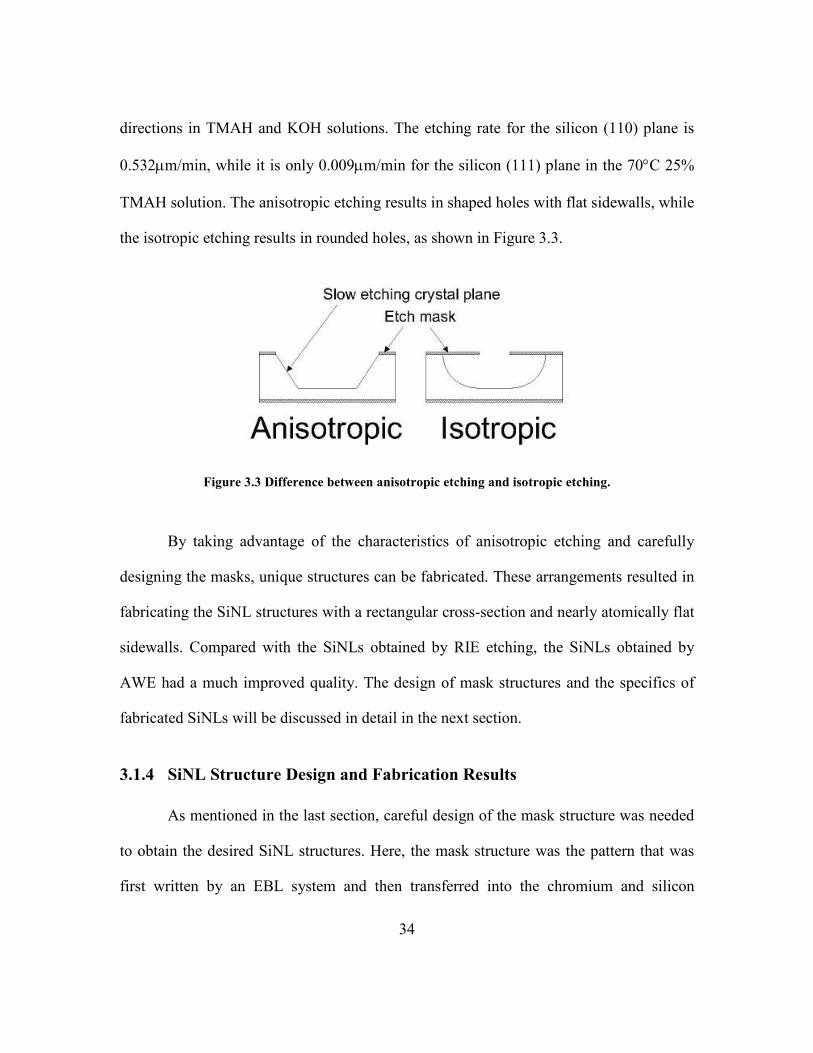
the isotropic etching results in rounded holes, as shown in Figure 3.3.
Figure 3.3 Difference between anisotropic etching and isotropic etching.
By taking advantage of the characteristics of anisotropic etching and carefully
designing the masks, unique structures can be fabricated. These arrangements resulted in
fabricating the SiNL structures with a rectangular cross-section and nearly atomically flat
sidewalls. Compared with the SiNLs obtained by RIE etching, the SiNLs obtained by
AWE had a much improved quality. The design of mask structures and the specifics of
fabricated SiNLs will be discussed in detail in the next section.
3.1.4 SiNL Structure Design and Fabrication Results
As mentioned in the last section, careful design of the mask structure was needed
to obtain the desired SiNL structures. Here, the mask structure was the pattern that was
first written by an EBL system and then transferred into the chromium and silicon
35
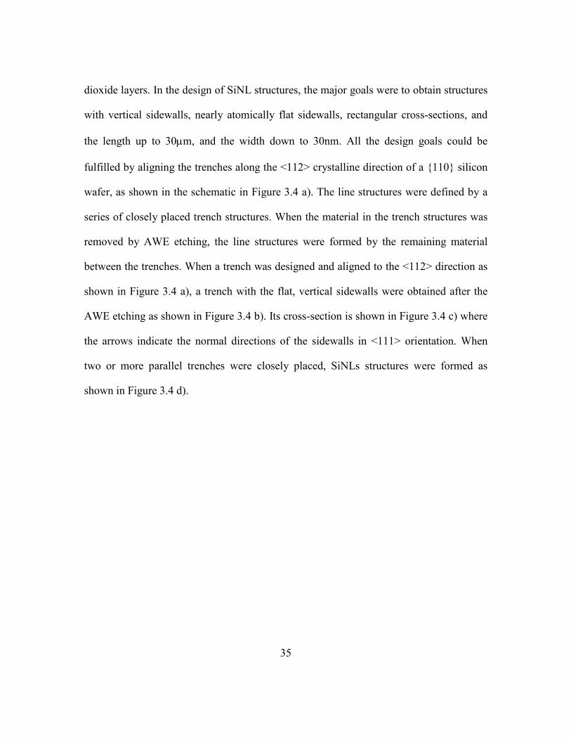
dioxide layers. In the design of SiNL structures, the major goals were to obtain structures
with vertical sidewalls, nearly atomically flat sidewalls, rectangular cross-sections, and
the length up to 30µm, and the width down to 30nm. All the design goals could be
fulfilled by aligning the trenches along the <112> crystalline direction of a {110} silicon
wafer, as shown in the schematic in Figure 3.4 a). The line structures were defined by a
series of closely placed trench structures. When the material in the trench structures was
removed by AWE etching, the line structures were formed by the remaining material
between the trenches. When a trench was designed and aligned to the <112> direction as
shown in Figure 3.4 a), a trench with the flat, vertical sidewalls were obtained after the
AWE etching as shown in Figure 3.4 b). Its cross-section is shown in Figure 3.4 c) where
the arrows indicate the normal directions of the sidewalls in <111> orientation. When
two or more parallel trenches were closely placed, SiNLs structures were formed as
shown in Figure 3.4 d).
36
Figure 3.4 a) Schematic of the mask design of SiNLs. b) A trench was formed by AWE. c) Schematic of cross-section of a trench. d) Formation of a SiNL between two trenches.
The key point of the design was to align the sidewalls of SiNLs to the <112>
direction of the {110} wafer. This problem was solved by two methods. The first method
was to find out the exact crystalline orientation of the silicon wafer. By this method, a set
of alignment marks were needed to be generated first, followed by writing a set of
orientation test structures. After the orientation test structures were carefully inspected
37
and the exact crystalline orientation was determined, an EBL alignment was performed
and the SiNLs structures were written. Although, by this method, all SiNLs were close to
the exact crystalline orientation and the product yield was much higher than the other
method, it required much more EBL writing and extra process steps. Therefore, the
second method discussed below was adopted for the research work in the laboratory.
In the second method, the fabrication process was simplified by designing a 10 by
10 structure array, which is shown in Figure 3.5 c). On each element of the array, the
SiNLs structures had the same orientation as shown in Figure 3.5 a). But there was an
orientation change between each element, starting from the lower-left corner at an angle
of -0.5° to the upper-right corner at an angle of +0.5°. In order to avoid the stitching
effect, the size of each element was 30µm X 30µm, smaller than the field size of the EBL
system, and the distance between the nearest neighbors was 160µm which was twice the
field size (80µm). This design ensured the writing of each element to be done in a single
field.
After all the RIE and pattern transfer steps and the AWE process, the element that
had the best orientation alignment to the intrinsic crystalline orientation of silicon wafer
was determined by SEM inspection. It is known that misalignment would cause bending,
distortion, and even cracking of the SiNL structures. The SiNLs with the best orientation
alignment had the best quality. Figure 3.5 b) shows an SEM image of a “good” SiNL
structure after the AWE process. Those SiNLs on the elements with the best orientation
alignment were selected for the nanoindentation experiments.
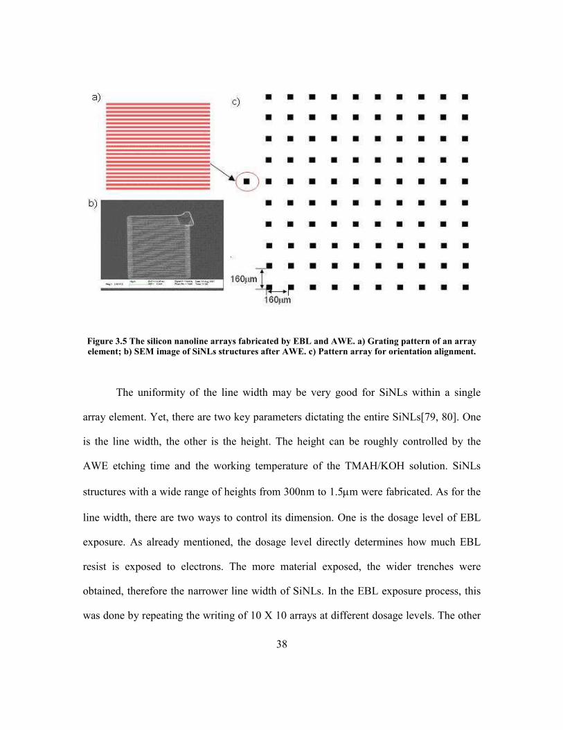
38
Figure 3.5 The silicon nanoline arrays fabricated by EBL and AWE. a) Grating pattern of an array element; b) SEM image of SiNLs structures after AWE. c) Pattern array for orientation alignment.
The uniformity of the line width may be very good for SiNLs within a single
array element. Yet, there are two key parameters dictating the entire SiNLs[79, 80]. One
is the line width, the other is the height. The height can be roughly controlled by the
AWE etching time and the working temperature of the TMAH/KOH solution. SiNLs
structures with a wide range of heights from 300nm to 1.5µm were fabricated. As for the
line width, there are two ways to control its dimension. One is the dosage level of EBL
exposure. As already mentioned, the dosage level directly determines how much EBL
resist is exposed to electrons. The more material exposed, the wider trenches were
obtained, therefore the narrower line width of SiNLs. In the EBL exposure process, this
was done by repeating the writing of 10 X 10 arrays at different dosage levels. The other
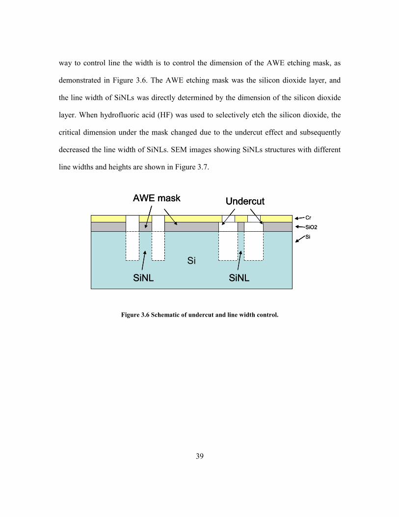
39
way to control line the width is to control the dimension of the AWE etching mask, as
demonstrated in Figure 3.6. The AWE etching mask was the silicon dioxide layer, and
the line width of SiNLs was directly determined by the dimension of the silicon dioxide
layer. When hydrofluoric acid (HF) was used to selectively etch the silicon dioxide, the
critical dimension under the mask changed due to the undercut effect and subsequently
decreased the line width of SiNLs. SEM images showing SiNLs structures with different
line widths and heights are shown in Figure 3.7.
Figure 3.6 Schematic of undercut and line width control.
Cr
SiO2
Si
Si
SiNLSiNL
UndercutAWE mask
Cr
SiO2
Si
Si
SiNLSiNL
UndercutAWE mask
Si
SiNLSiNLSiNLSiNL
UndercutAWE mask
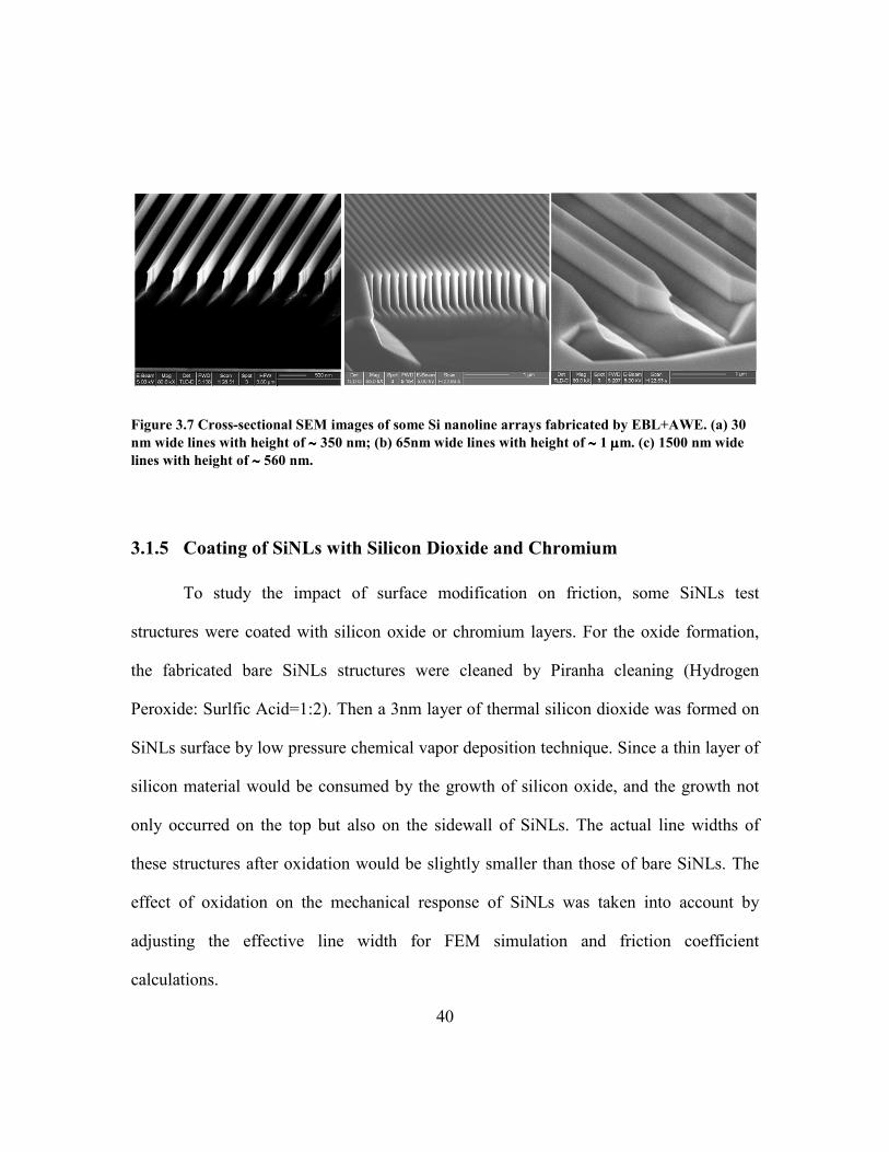
40
Figure 3.7 Cross-sectional SEM images of some Si nanoline arrays fabricated by EBL+AWE. (a) 30 nm wide lines with height of ∼∼∼∼ 350 nm; (b) 65nm wide lines with height of ∼∼∼∼ 1 µµµµm. (c) 1500 nm wide lines with height of ∼∼∼∼ 560 nm.
3.1.5 Coating of SiNLs with Silicon Dioxide and Chromium
To study the impact of surface modification on friction, some SiNLs test
structures were coated with silicon oxide or chromium layers. For the oxide formation,
the fabricated bare SiNLs structures were cleaned by Piranha cleaning (Hydrogen
Peroxide: Surlfic Acid=1:2). Then a 3nm layer of thermal silicon dioxide was formed on
SiNLs surface by low pressure chemical vapor deposition technique. Since a thin layer of
silicon material would be consumed by the growth of silicon oxide, and the growth not
only occurred on the top but also on the sidewall of SiNLs. The actual line widths of
these structures after oxidation would be slightly smaller than those of bare SiNLs. The
effect of oxidation on the mechanical response of SiNLs was taken into account by
adjusting the effective line width for FEM simulation and friction coefficient
calculations.
41
After finishing the nanoindentation experiments on SiO2 coated SiNLs structures,
a 2nm layer of chromium was deposited on the SiNLs by the electron-beam evaporation
system. The chromium layer was deposited mostly on top of the SiNLs.
3.2 NanoMechanical Testing System
The NanoMechanical Testing System was based on a multi-mode AFM system.
Equipped with a 2D-Transducer, this system had both the capabilities of nanoindentation
tests and nanoscratching tests. The nanoindentation technique was extensively employed
for the study of SiNLs and will be reviewed here.
Compared with other methods such as microbeam cantilever tests or bulge tests,
nanoindentation is a more convenient technique, because there is less stringent
requirement for sample preparation. Figure 3.8 shows a schematic of the nanoindentation
process. First, the sample surface was imaged in conventional AFM mode with a
diamond indenter and the positions for the indentation were selected. Then, the loading
and unloading process, with the simultaneous force and displacement measurement, was
monitored and recorded using a transducer. A second AFM image of the surface may be
used to examine the shape of the indent after the indentation. Since the depth resolution
was on the order of nanometers, it was possible to indent the thin, low-k films with sub-
micron thickness. Figure 3.9 shows SEM images of three types of indenters. Among
these, the Berkovich indenter is the most widely used to extract both elastic modulus and
hardness from the force vs. displacement curves.
Oliver and Pharr proposed an analysis method, with which the elastic modulus, E,
and hardness, H, can be derived directly from the analysis of the unloading force vs.
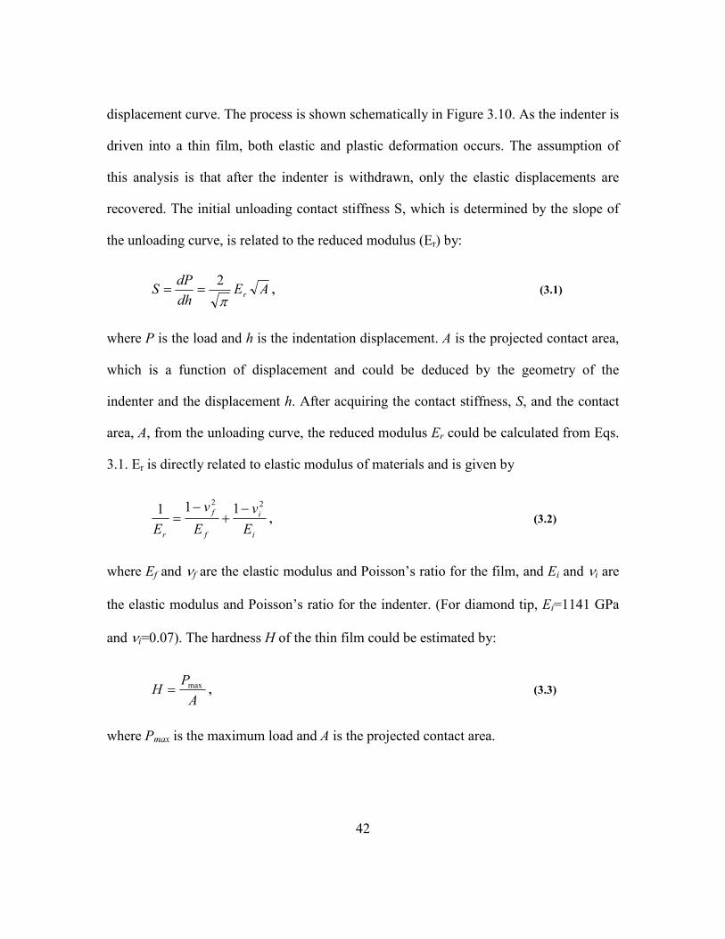
42
displacement curve. The process is shown schematically in Figure 3.10. As the indenter is
driven into a thin film, both elastic and plastic deformation occurs. The assumption of
this analysis is that after the indenter is withdrawn, only the elastic displacements are
recovered. The initial unloading contact stiffness S, which is determined by the slope of
the unloading curve, is related to the reduced modulus (Er) by:
AEdhdP
S rπ2
== , (3.1)
where P is the load and h is the indentation displacement. A is the projected contact area,
which is a function of displacement and could be deduced by the geometry of the
indenter and the displacement h. After acquiring the contact stiffness, S, and the contact
area, A, from the unloading curve, the reduced modulus Er could be calculated from Eqs.
3.1. Er is directly related to elastic modulus of materials and is given by
i
i
f
f
r Ev
E
v
E
22 111 −+
−= , (3.2)
where Ef and νf are the elastic modulus and Poisson’s ratio for the film, and Ei and νi are
the elastic modulus and Poisson’s ratio for the indenter. (For diamond tip, Ei=1141 GPa
and νi=0.07). The hardness H of the thin film could be estimated by:
A
PH max= , (3.3)
where Pmax is the maximum load and A is the projected contact area.
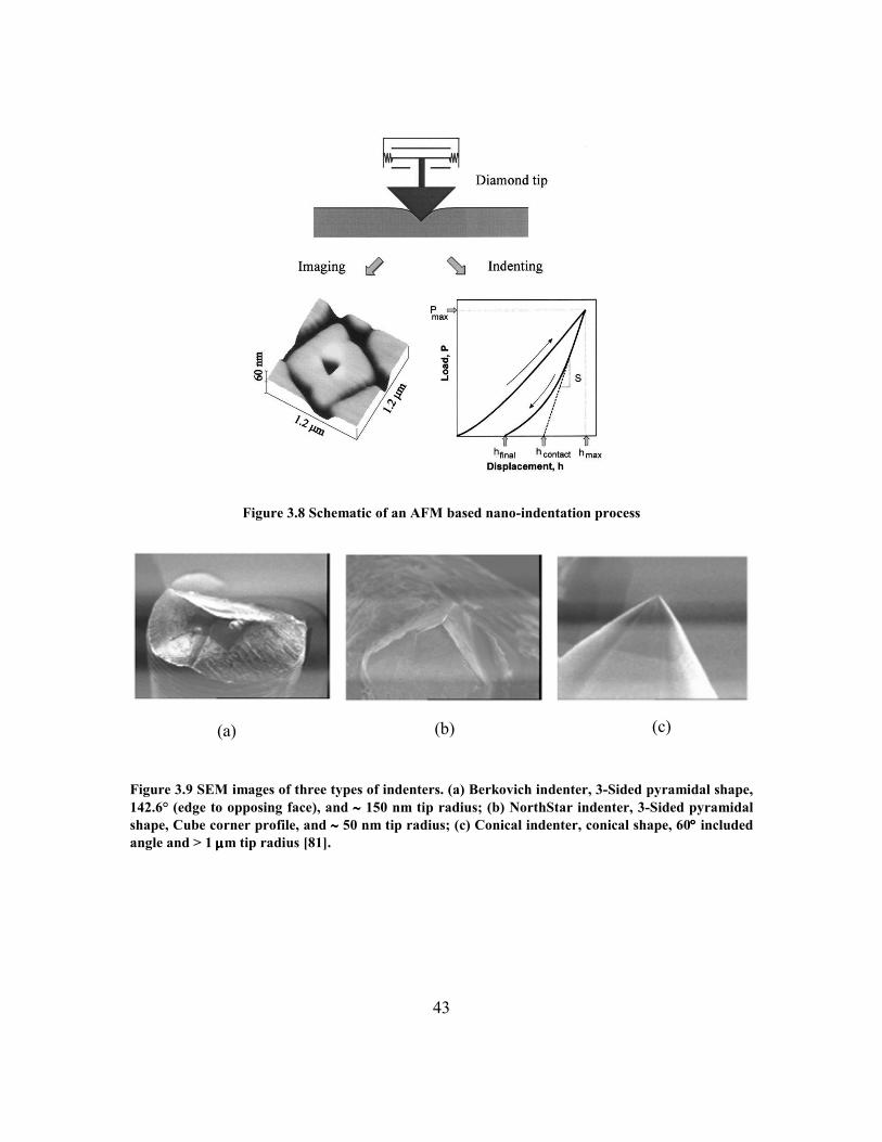
43
(a) (b) (c)
Figure 3.8 Schematic of an AFM based nano-indentation process
Figure 3.9 SEM images of three types of indenters. (a) Berkovich indenter, 3-Sided pyramidal shape, 142.6° (edge to opposing face), and ∼∼∼∼ 150 nm tip radius; (b) NorthStar indenter, 3-Sided pyramidal shape, Cube corner profile, and ∼∼∼∼ 50 nm tip radius; (c) Conical indenter, conical shape, 60°°°° included angle and > 1 µµµµm tip radius [81].
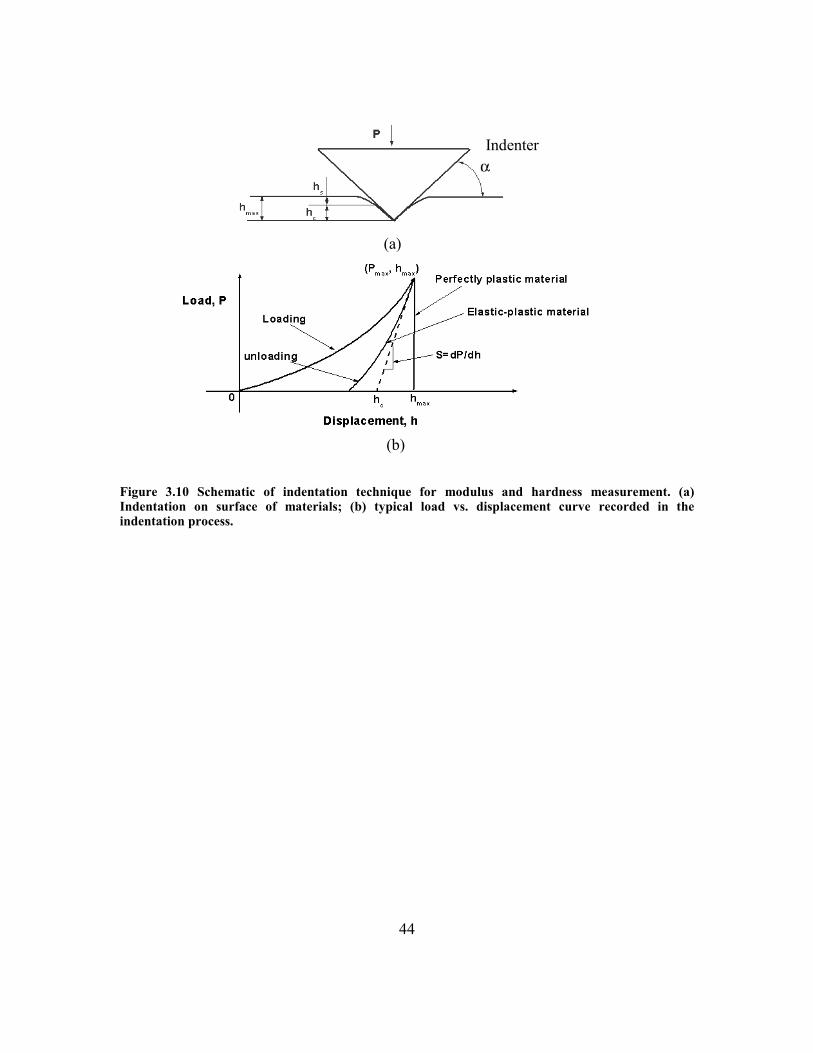
44
Figure 3.10 Schematic of indentation technique for modulus and hardness measurement. (a) Indentation on surface of materials; (b) typical load vs. displacement curve recorded in the indentation process.
(a)
(b)
Indenter
45
Chapter 4: Analysis of Buckling Behavior of SiNLs
In this chapter, the focus is on the mechanical response of high aspect ratio SiNLs
under nanoindentation. The Nano-indentation technique was combined with finite
element method (FEM) with the latter to simulate the indentation process. Material
properties of SiNLs, e.g. elastic modulus and strain to failure, were extracted from the
simulation. The metrology was also used to evaluate friction between indenter and
SiNLs, and the results indicated that this approach can be used to study friction behavior
at nano-metric scale.
This chapter starts with an analysis of a set of typical experimental load-
displacement curves. During indentation, a buckling instability was observed at a critical
load, followed by a displacement burst without a load increase, then a fully recoverable
deformation upon unloading. For experiments with larger indentation displacements,
irrecoverable indentation displacements were observed due to fracture of Si nanolines.
The strain to failure was estimated by FEM simulation to be as high as 7%[79], which is
much larger than 0.25-0.5% of its bulk[37]. An analytical model is also developed for
further understanding of the buckling behavior, e.g. post-buckling modes, critical
buckling load, etc, of a set of SiNLs. These analyses indicated that the buckling behavior
of SiNLs depends on the combined effects of load, line geometry such as height to width
aspect ratio, the width to pitch ratio, etc, and the friction at contact.
46
4.1 FEM Simulation of Nanoindentation on SiNLs
The friction force, if exists, provides additional constraints to the SiNLs at the
contacting surfaces and changes the boundary conditions of the bending and buckling
problems we formulated in Chapter 2. As it can be predicted, the existence of friction
may change the mechanical responses of SiNLs under nanoindentation. Specifically, the
friction may change the buckling behavior of SiNLs in our experiments. To evaluate the
friction effect in the buckling behavior of SiNLs, an FEM model was developed by Li et.
al.[79].
FEM is widely used for the simulation analysis of experimental results for the
study of material properties under indentation[36, 38, 82]. The unknown material
properties are determined by first using them as input parameters in FEM model until
best fit to the experimental load-displacement curves is obtained. Then the indentation
process details could be examined accordingly.
In this section, the FEM model for the 75nm SiNLs test structures will be
discussed. The normal procedures to extract the friction coefficient for the experimental
load-displacement curves will be demonstrated. These procedures will be followed in our
data analysis for other SiNLs test structures.
4.1.1 FEM Model
The FEM model of nanoindentation on SiNLs is shown in Figure 4.1. Twelve
parallel lines were modeled as SiNLs. The tip of the indenter was located at the trench
center. The diamond indenter is simulated as a rigid sphere, since it has much higher
modulus (1140 GPa) than silicon (163 GPa). The modulus of silicon is assumed to be the
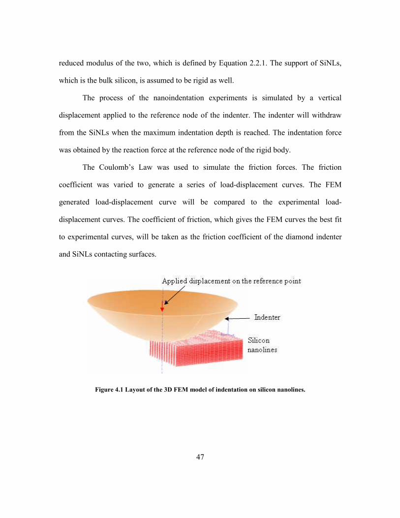
47
reduced modulus of the two, which is defined by Equation 2.2.1. The support of SiNLs,
which is the bulk silicon, is assumed to be rigid as well.
The process of the nanoindentation experiments is simulated by a vertical
displacement applied to the reference node of the indenter. The indenter will withdraw
from the SiNLs when the maximum indentation depth is reached. The indentation force
was obtained by the reaction force at the reference node of the rigid body.
The Coulomb’s Law was used to simulate the friction forces. The friction
coefficient was varied to generate a series of load-displacement curves. The FEM
generated load-displacement curve will be compared to the experimental load-
displacement curves. The coefficient of friction, which gives the FEM curves the best fit
to experimental curves, will be taken as the friction coefficient of the diamond indenter
and SiNLs contacting surfaces.
Figure 4.1 Layout of the 3D FEM model of indentation on silicon nanolines.
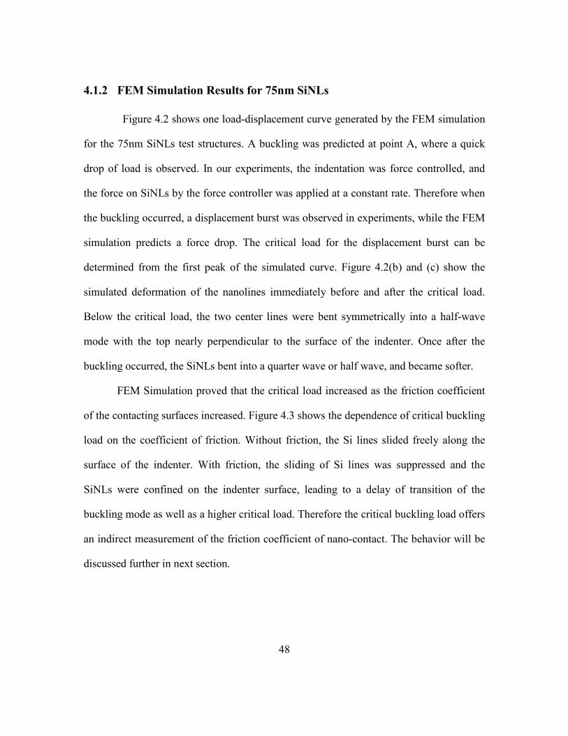
48
4.1.2 FEM Simulation Results for 75nm SiNLs
Figure 4.2 shows one load-displacement curve generated by the FEM simulation
for the 75nm SiNLs test structures. A buckling was predicted at point A, where a quick
drop of load is observed. In our experiments, the indentation was force controlled, and
the force on SiNLs by the force controller was applied at a constant rate. Therefore when
the buckling occurred, a displacement burst was observed in experiments, while the FEM
simulation predicts a force drop. The critical load for the displacement burst can be
determined from the first peak of the simulated curve. Figure 4.2(b) and (c) show the
simulated deformation of the nanolines immediately before and after the critical load.
Below the critical load, the two center lines were bent symmetrically into a half-wave
mode with the top nearly perpendicular to the surface of the indenter. Once after the
buckling occurred, the SiNLs bent into a quarter wave or half wave, and became softer.
FEM Simulation proved that the critical load increased as the friction coefficient
of the contacting surfaces increased. Figure 4.3 shows the dependence of critical buckling
load on the coefficient of friction. Without friction, the Si lines slided freely along the
surface of the indenter. With friction, the sliding of Si lines was suppressed and the
SiNLs were confined on the indenter surface, leading to a delay of transition of the
buckling mode as well as a higher critical load. Therefore the critical buckling load offers
an indirect measurement of the friction coefficient of nano-contact. The behavior will be
discussed further in next section.
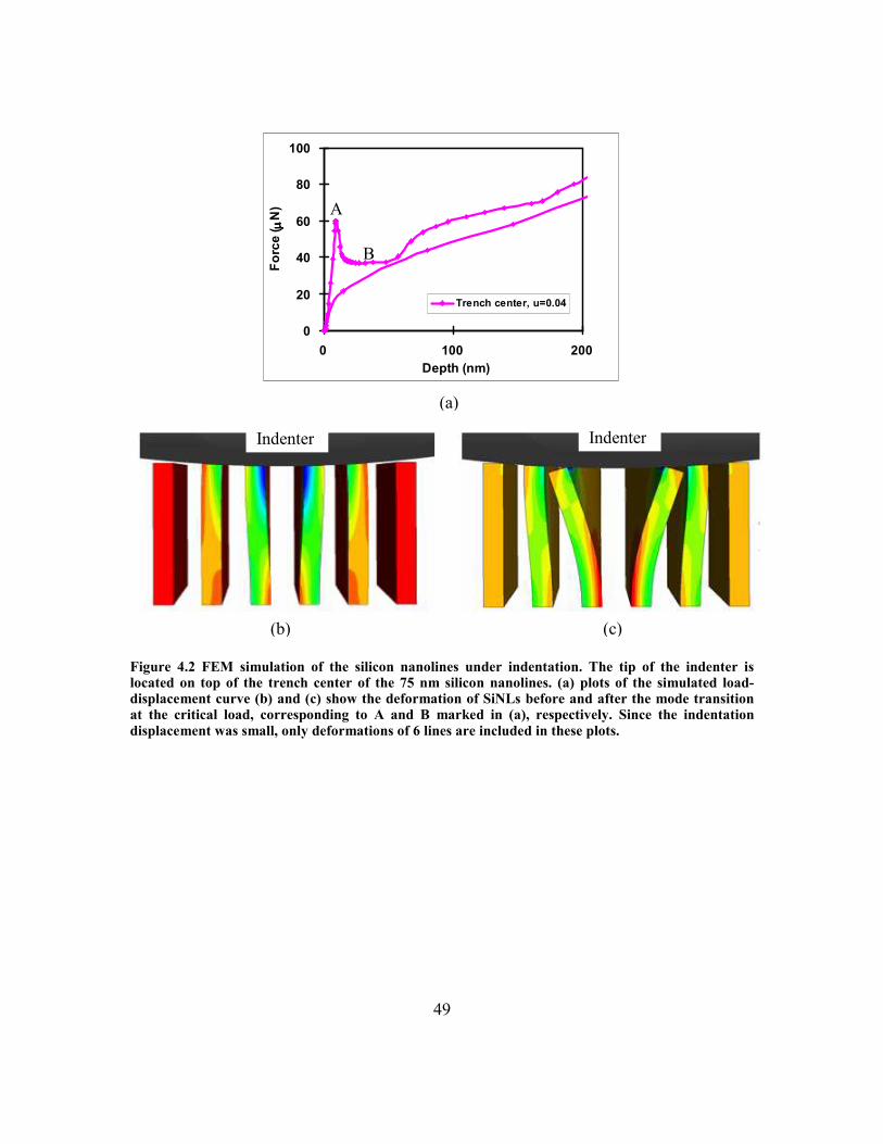
49
0
20
40
60
80
100
0 100 200Depth (nm)
Force ( µµ µµN)
Trench center, u=0.04
Figure 4.2 FEM simulation of the silicon nanolines under indentation. The tip of the indenter is located on top of the trench center of the 75 nm silicon nanolines. (a) plots of the simulated load-displacement curve (b) and (c) show the deformation of SiNLs before and after the mode transition at the critical load, corresponding to A and B marked in (a), respectively. Since the indentation displacement was small, only deformations of 6 lines are included in these plots.
(a)
(b) (c)
Indenter Indenter
A
B
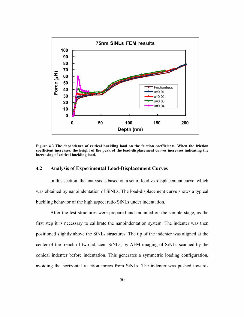
50
75nm SiNLs FEM results
0102030405060708090100
0 50 100 150 200Depth (nm)
Force ( µµ µµN)
Frictionlessu=0.01u=0.02u=0.03u=0.04
Figure 4.3 The dependence of critical buckling load on the friction coefficients. When the friction coefficient increases, the height of the peak of the load-displacement curves increases indicating the increasing of critical buckling load.
4.2 Analysis of Experimental Load-Displacement Curves
In this section, the analysis is based on a set of load vs. displacement curve, which
was obtained by nanoindentation of SiNLs. The load-displacement curve shows a typical
buckling behavior of the high aspect ratio SiNLs under indentation.
After the test structures were prepared and mounted on the sample stage, as the
first step it is necessary to calibrate the nanoindentation system. The indenter was then
positioned slightly above the SiNLs structures. The tip of the indenter was aligned at the
center of the trench of two adjacent SiNLs, by AFM imaging of SiNLs scanned by the
conical indenter before indentation. This generates a symmetric loading configuration,
avoiding the horizontal reaction forces from SiNLs. The indenter was pushed towards
51
sample surface vertically until a contact between indenter and SiNLs was initiated. As the
indention continued, the SiNLs structures deformed until a designated maximum
indentation force was reached. Finally, after withdraw of the indenter, SiNLs were
separated from indenter. The reaction forces of the SiNLs were recorded to generate a
load vs. displacement curve. The first contact occurred between the indenter and the two
adjacent SiNLs leading to an increase of the reaction force as the indentation depth
advanced, which is shown in a typical load vs. displacement curve (before mark “a”) in
Figure 4.4 a). This set of load-displacement curve was obtained from the indentation test
on a set of SiNLs, having 60 nm linewidth and 640 nm line height with an aspect ratio as
high as 10.6. At the initial stage of deformation, the two SiNLs in contact with the
indenter were elastically deformed. The SiNLs were pinned on the surface of indenter if
frictional force is strong enough. The reaction force increased with further increase of
displacement, until a displacement burst was observed, which was attributed to the onset
of buckling instability (Marked “a” in Figure 4.4a). The reaction force at point “a” is
defined as the critical load for the buckling of SiNLs, or critical buckling load.
The load-displacement curve is divided into four different regions, corresponding
to four different stages of the FEM model which are shown in Figure 4.4b)-e). At the first
stage, when the applied load was small, the SiNLs structures exhibited an elastic
response, as shown by the green segment of the curve. This elastic response was
correlated to the FEM model in Figure 4.4b). As the applied load increased, a
displacement burst occurred. The displacement burst reflects a structural instability of the
SiNLs when subjected to a sufficiently large applied load. At this point, the high aspect
ratio SiNLs usually demonstrated a buckling behavior, with one of the possible buckling
52
modes as shown schematically in Figure 4.4 c). After buckling, the SiNLs may regain
some structure strength, and the applied load increases gradually. This corresponds to the
load-displacement curve marked by yellow and the deformation behavior in Figure 4.4d),
showing that the two SiNLs bent outwards to the indenter and slided on the indenter
surface. In the final stage, the indenter was withdrawn as indicated in the red region of
the load-displacement curve, which corresponded to deformation behavior in Figure
4.4e). In this case, it was found that the displacement of SiNLs could fully recover
without a residual deformation. It is also observed that further increase of the applied
load would eventually lead to fracture of SiNLs. A typical indentation curve showing
residual deformation left after indentation, and the corresponding SEM image revealing
the fracture of SiNLs and debris of broken pieces, are shown in Figure 4.5 (a) and Figure
4.5(b), respectively.
The two possible buckling modes, Mode I and Mode II, are schematically
demonstrated in Figure 4.7 and Figure 4.8. At the critical buckling load, softening of the
nanolines under the indentation would lead to a displacement burst during a load-control
experiment. In the Figure 4.7, the SiNLs are bent into a quarter-wave mode, due to a lack
of constraint on the top ends of lines. In Figure 4.8, the center two lines are bent
symmetrically into a half-wave mode with the top nearly perpendicular to the surface of
the indenter, which is structurally stiffer than the half-wave Mode I and should have a
higher critical load under the same geometry condition. It is shown that the buckling
mode selection is close related to constraint boundary condition, which is determined by
the line geometry and friction properties at the contact.

53
The impact of geometry and friction on the structure buckling mode will be
further discussed in Section 4.3. The predicted mapping of line geometry, friction at
contact vs. buckling mode, matches well with the experimental results, showing the
validity of the buckling analysis.
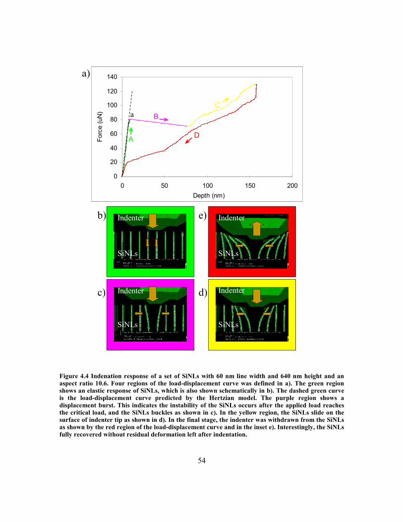
54
Figure 4.4 Indenation response of a set of SiNLs with 60 nm line width and 640 nm height and an aspect ratio 10.6. Four regions of the load-displacement curve was defined in a). The green region shows an elastic response of SiNLs, which is also shown schematically in b). The dashed green curve is the load-displacement curve predicted by the Hertzian model. The purple region shows a displacement burst. This indicates the instability of the SiNLs occurs after the applied load reaches the critical load, and the SiNLs buckles as shown in c). In the yellow region, the SiNLs slide on the surface of indenter tip as shown in d). In the final stage, the indenter was withdrawn from the SiNLs as shown by the red region of the load-displacement curve and in the inset e). Interestingly, the SiNLs fully recovered without residual deformation left after indentation.
0
20
40
60
80
100
120
140
0 50 100 150 200
Depth (nm)
Force (uN
)
A
B
C
D
a)
b)
c)
e)
d)
a
Indenter Indenter
Indenter Indenter
SiNLs SiNLs
SiNLs SiNLs
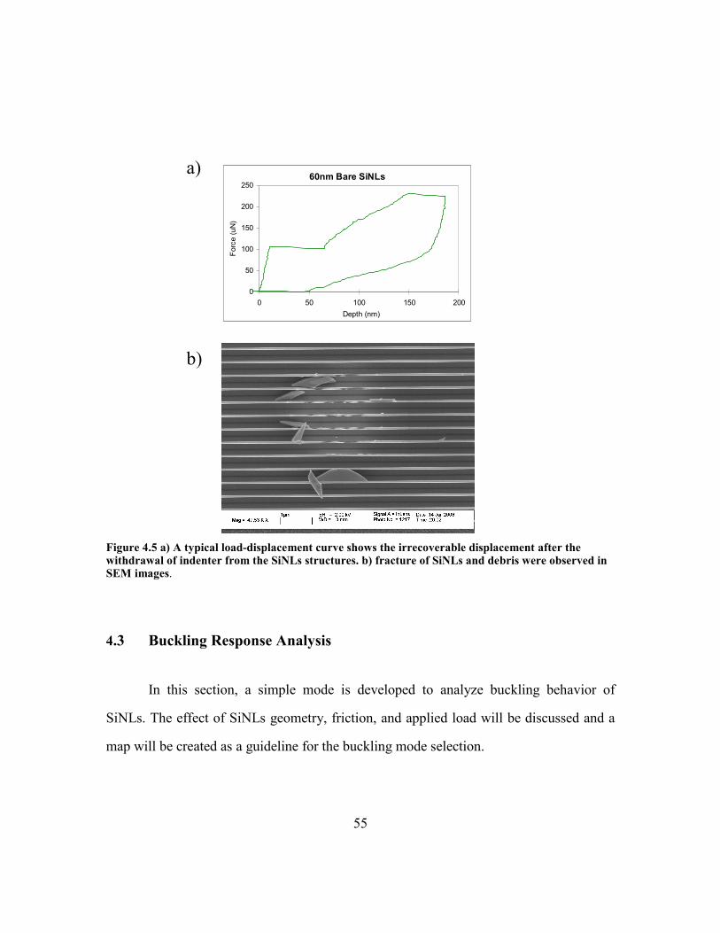
55
Figure 4.5 a) A typical load-displacement curve shows the irrecoverable displacement after the withdrawal of indenter from the SiNLs structures. b) fracture of SiNLs and debris were observed in SEM images.
4.3 Buckling Response Analysis
In this section, a simple mode is developed to analyze buckling behavior of
SiNLs. The effect of SiNLs geometry, friction, and applied load will be discussed and a
map will be created as a guideline for the buckling mode selection.
a)
b)
60nm Bare SiNLs
0
50
100
150
200
250
0 50 100 150 200
Depth (nm)
Force (uN
)
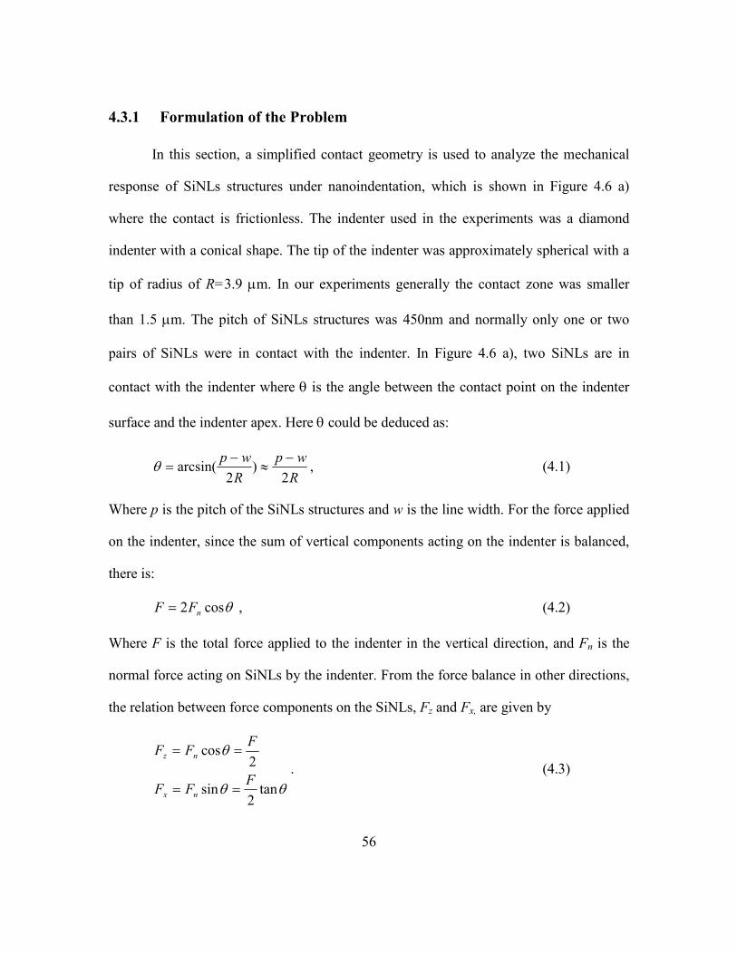
56
4.3.1 Formulation of the Problem
In this section, a simplified contact geometry is used to analyze the mechanical
response of SiNLs structures under nanoindentation, which is shown in Figure 4.6 a)
where the contact is frictionless. The indenter used in the experiments was a diamond
indenter with a conical shape. The tip of the indenter was approximately spherical with a
tip of radius of R=3.9 µm. In our experiments generally the contact zone was smaller
than 1.5 µm. The pitch of SiNLs structures was 450nm and normally only one or two
pairs of SiNLs were in contact with the indenter. In Figure 4.6 a), two SiNLs are in
contact with the indenter where θ is the angle between the contact point on the indenter
surface and the indenter apex. Here θ could be deduced as:
Rwp
Rwp
2)
2arcsin(
−≈
−=θ , (4.1)
Where p is the pitch of the SiNLs structures and w is the line width. For the force applied
on the indenter, since the sum of vertical components acting on the indenter is balanced,
there is:
θcos2 nFF = , (4.2)
Where F is the total force applied to the indenter in the vertical direction, and Fn is the
normal force acting on SiNLs by the indenter. From the force balance in other directions,
the relation between force components on the SiNLs, Fz and Fx, are given by
θθ
θ
tan2
sin
2cos
FFF
FFF
nx
nz
==
==. (4.3)
57
where the xyz coordinate system is defined as shown in the lower-left inset of Figure 4.6
a).
Consider under the condition of existence of frictional forces at the contact
surfaces, the force components are to be modified as:
θθ
θθ
cossin2
sincos
fnx
fnz
FFF
FFFF
−=
=+= , (4.4)
where Ff is the frictional force which is tangent to the diamond surface at the contact.
Rearranging Equation 4.4 and defining Ff=µ�Fn , according to the Coulomb’s Law, we
have
1tan and 1h wit)(tan2
tan1tan
2
2
<<<<−≈
+−
=
=
θµθµθ
θµµθ
F
FF
FF
x
z
. (4.5)
In the following text, the coefficient θµµθ
tan1tan+
− will be denoted as Q for
convenience.
For clarification, the details of the undeformed line geometry are shown in Figure
4.6 b). The SiNLs is eccentrically loaded at the upper-left corner with Fz acting at a
distance w/2 away from the axis of SiNLs. It should be noted that the “friction
coefficient” µ as defined is only a static friction coefficient assuming that the SiNLs were
not sliding on the indenter surface. Once sliding occurs, the friction coefficient µ will
become smaller than the static friction coefficient, which is determined by the lateral
58
forces. Therefore this “friction coefficient” represents the static friction coefficient before
transition to sliding friction from static state.
Figure 4.6 Contact geometry of nanoindentation. The shape of the diamond indenter was conical but it was modeled as a sphere with a radius R of 3.9 µµµµm. In the picture, two SiNLs were shown in contact with the indenter. θθθθ is the angle that measure the relative place of the contact point on the indenter. F is the total force applied on the indenter in the vertical direction. Fn is the force on SiNLs that was normal to the indenter surface.
4.3.2 Buckling Modes and Critical Loads Analysis
PP ww
SiNLs
R
O
RR
O
nFnF
FF θθ
x
z
y
o x
z
y
o
Fz
Fx x
z
w/2
Fz
Fx x
z
w/2
a)
b)
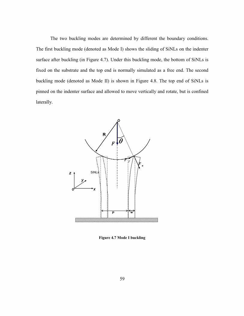
59
The two buckling modes are determined by different the boundary conditions.
The first buckling mode (denoted as Mode I) shows the sliding of SiNLs on the indenter
surface after buckling (in Figure 4.7). Under this buckling mode, the bottom of SiNLs is
fixed on the substrate and the top end is normally simulated as a free end. The second
buckling mode (denoted as Mode II) is shown in Figure 4.8. The top end of SiNLs is
pinned on the indenter surface and allowed to move vertically and rotate, but is confined
laterally.
Figure 4.7 Mode I buckling
PP ww
SiNLs
fFnF
fF fFnF nF
F
R
O
θFF
R
O
θR
O
RR
O
θθ
x
z
y
o x
z
y
o
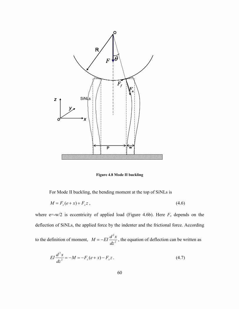
60
Figure 4.8 Mode II buckling
For Mode II buckling, the bending moment at the top of SiNLs is
zFxeFM xz ++= )( , (4.6)
where e=-w/2 is eccentricity of applied load (Figure 4.6b). Here Fx depends on the
deflection of SiNLs, the applied force by the indenter and the frictional force. According
to the definition of moment, 2
2
dzxd
EIM −= , the equation of deflection can be written as
zFxeFMdz
xdEI xz −+−=−= )(2
2
. (4.7)
PP ww
SiNLs
fFnF
fFfFnFnF
F
R
O
θFF
R
O
θR
O
RR
O
θθ
x
z
y
o x
z
y
o
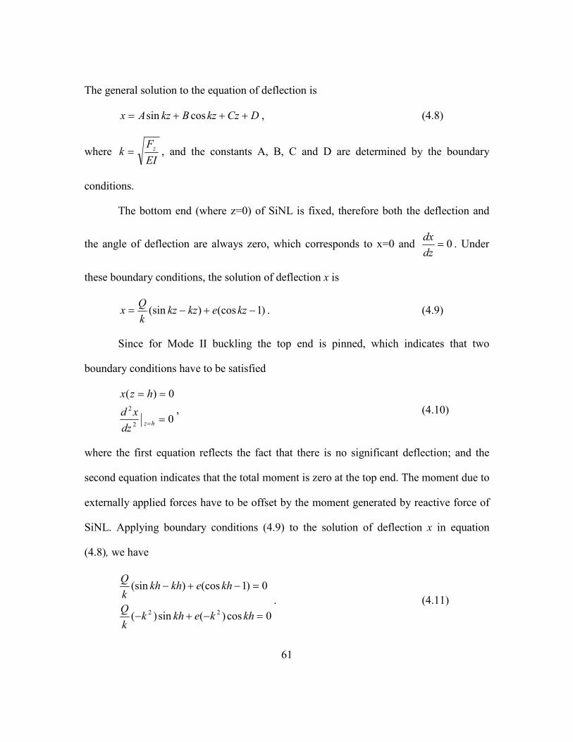
61
The general solution to the equation of deflection is
DCzkzBkzAx +++= cossin , (4.8)
where EIF
k z= , and the constants A, B, C and D are determined by the boundary
conditions.
The bottom end (where z=0) of SiNL is fixed, therefore both the deflection and
the angle of deflection are always zero, which corresponds to x=0 and 0=dzdx
. Under
these boundary conditions, the solution of deflection x is
)1(cos)(sin −+−= kzekzkzkQ
x . (4.9)
Since for Mode II buckling the top end is pinned, which indicates that two
boundary conditions have to be satisfied
0
0)(
2
2
=
==
=hzdzxd
hzx, (4.10)
where the first equation reflects the fact that there is no significant deflection; and the
second equation indicates that the total moment is zero at the top end. The moment due to
externally applied forces have to be offset by the moment generated by reactive force of
SiNL. Applying boundary conditions (4.9) to the solution of deflection x in equation
(4.8), we have
0cos)(sin)(
0)1(cos)(sin
22 =−+−
=−+−
khkekhkkQ
khekhkhkQ
. (4.11)
62
After simplifying the above equations, we obtain
he
Q
khkh
=
=tan, (4.12)
where the first equation can be solved numerically and the smallest positive solution for
kh is found to be 4.493, therefore the critical buckling load is
2
2
_
493.4h
EIF crz = . (4.13)
According to the definition of EIF
k z= . This critical buckling load has the same
value as that given in Chapter 2, where there is no external lateral load Fx and the
eccentricity of applied load is zero, but in both cases, the boundary conditions are the
same because the top end of SiNLs is pinned.
The second equation, he
Q = , provides the requirement for the frictional force to
satisfy the boundary conditions. Recall that we defined µθθµµθ
−≈+
−= tan
tan1tan
Q in
Equation (4.4), and 2w
e −= , therefore
R
wph
wh
w22
tan2
−+≈+= θµ . (4.14)
Only when the friction coefficient µ is larger than this value can the frictional
force provide enough constraint to pin the SiNLs on the indenter surface before the
initiation of Mode II buckling. When µ is smaller than equation 4.14, sliding may occur
before the occurrence of Mode II buckling.
63
For Mode I buckling, since the system is eccentrically loaded and a lateral force
exists, there is a deflection of the top of SiNL even before the occurrence of buckling. As
shown in Figure 4.4, a deflection, δ, is assumed at the top of SiNLs. By considering the
deflection, the bending moment in equation 4.6 is:
zFxeFM xz +++−= )( δ
Following the same procedure and boundary conditions for the bottom end of
SiNLs, the solution of the equation of deflection (equation 4.7) is solved to be
)1)(cos()(sin −+−+−= kzekzkzkQ
x δ , (4.15)
which is very similar to equation 4.9. Equation 4.15 need to satisfy the assumption that
the deflection of SiNL at the top end is δ, therefore,
δδ =−+−+−= )1)(cos()(sin)( khekhkhkQ
hx , (4.16)
from which the deflection δ can be solved as
kh
khkhkQ
khkh
ecos
sincos
1cos −+
−=δ . (4.17)
Equation 4.17 is derived as a superposition of solutions for a purely eccentrically
loaded beam and purely laterally loaded buckling beam. From equation 4.17, it is clear
that when coskh=0, the deflection mathematically reaches infinite which indicates the
unstable state where buckling occurs. The critical buckling load can be solved from
coskh=0,
2
2
_ 4hEI
F crz
π= , (4.18)
64
which is the same as given solved in Chapter 2 under the condition of no eccentric or
lateral load.
For the boundary conditions in Mode I buckling are applied, the top end of the
SiNL is free and the total force and total moment is zero. These conditions lead to the
following equation for the deflection along the x direction when, z=h:
03
3
2
2
==dz
xddz
xd.
The solutions of this equation are defined by the following conditions:
0sin)(cos
0cos)(sin
=−−
=−+
khkekhQ
khkekhQ
δδ
.
These two equations are true only when Q=0, indicating Fx=0. This corresponds to the
condition where the top end of the SiNL is considered to be “free”. When Q=0, we
deduce the friction coefficient µ to be:
R
wp2
tan−
≈≈ θµ .
Accordingly, the friction behavior at the contact can be divided into three regions with
−≤
−+≤≤
−
−+≥
(4.19c) 2
(4.19b) 222
(4.19a) 22
Rwp
Rwp
hw
Rwp
Rwp
hw
µ
µ
µ
Different buckling behaviors will occur depending on in which regime the friction
coefficient belongs. These regions are defined according to the geometry of the SiNLs,
65
e.g. height to width aspect ratio, and the width to pitch ratio, etc. The effect of geometry
on the buckling behavior is further discussed in the following section.
4.3.3 The Effect of Geometry and Friction on Buckling Behavior
For convenience, the height to width aspect ratio is denoted as AR, and the width
to pitch ratio is denoted as WP, we have:
pw
WP
wh
AR
=
=.
Then the regions of friction coefficient can be expressed as
−≤
−+≤≤
−
−+≥
(4.20c) 2
)1(
(4.20b) 2
)1(21
2)1(
(4.20a) 2
)1(21
RWPp
RWPp
ARRWPp
RWPp
AR
µ
µ
µ
Equation 4.20a expresses the conditions for Mode II buckling to occur. The effect
of AR and WP is plotted in Figure 4.9. There are two sets of curves in Figure 4.9, which
divide the area of the graph into three regions, as marked by A, B and C. The set of
straight lines corresponds to the condition that Q=0 and with the top end of SiNL being
free, where RWPp
2)1( −
=µ . The other set of curves corresponds to the condition that the
top end of SiNL is pinned on the indenter surface, and Rwp
hw
hw
22tan
2−
+≈+= θµ .
66
As the height to width aspect ratio (AR) increases, the required coefficient of
friction to initiate the Mode II buckling becomes smaller. This can be seen from the result
of the 70nm test structures which has an AR=8.7, the coefficient of friction required for
Mode II buckling to occur for this structure is 0.107. In comparison, with the AR of the
90nm test structure increasing to 15.5, the required coefficient of friction for Mode II
buckling decreases to 0.078. If the actual coefficient of friction is smaller than this value,
it is highly probable that the Mode II buckling will not be observed for the 90nm test
structure. Accordingly, Mode II buckling would be less probable to occur for the 70nm
and 60nm test structures, considering the coefficient of friction between diamond and
silicon is low and may not reach a value of 0.1. Table 4.1 summarizes the required
coefficients of friction for Mode II buckling for all test structures on which
nanoindentation experiments were performed. The results were confirmed by the
experimental observation, which shows that Mode II buckling was only observed for
90nm and 75nm test structures.
Based on this analysis, the required coefficient of friction for 30nm test structures
for Mode II is the smallest. However, Mode II buckling was not experimentally observed.
This indicates that the actual coefficient of friction for this set of test structures is smaller
than 0.075. In Chapter 5, this phenomenon is further analyzed, which indicates that the
coefficient of friction for 30nm test structures is smaller than those of other test
structures.
The width to pitch ratio (WP) will also affect the buckling behavior. Based on
above analysis, if the height to width aspect ratio is kept constant while the dimension of
SiNL is scaled down, Mode II buckling would be less likely to be observed. When the
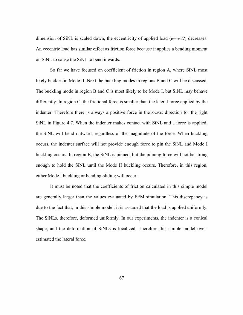
67
dimension of SiNL is scaled down, the eccentricity of applied load (e=-w/2) decreases.
An eccentric load has similar effect as friction force because it applies a bending moment
on SiNL to cause the SiNL to bend inwards.
So far we have focused on coefficient of friction in region A, where SiNL most
likely buckles in Mode II. Next the buckling modes in regions B and C will be discussed.
The buckling mode in region B and C is most likely to be Mode I, but SiNL may behave
differently. In region C, the frictional force is smaller than the lateral force applied by the
indenter. Therefore there is always a positive force in the x-axis direction for the right
SiNL in Figure 4.7. When the indenter makes contact with SiNL and a force is applied,
the SiNL will bend outward, regardless of the magnitude of the force. When buckling
occurs, the indenter surface will not provide enough force to pin the SiNL and Mode I
buckling occurs. In region B, the SiNL is pinned, but the pinning force will not be strong
enough to hold the SiNL until the Mode II buckling occurs. Therefore, in this region,
either Mode I buckling or bending-sliding will occur.
It must be noted that the coefficients of friction calculated in this simple model
are generally larger than the values evaluated by FEM simulation. This discrepancy is
due to the fact that, in this simple model, it is assumed that the load is applied uniformly.
The SiNLs, therefore, deformed uniformly. In our experiments, the indenter is a conical
shape, and the deformation of SiNLs is localized. Therefore this simple model over-
estimated the lateral force.
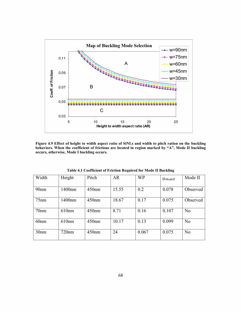
68
Figure 4.9 Effect of height to width aspect ratio of SiNLs and width to pitch ration on the buckling behaviors. When the coefficient of frictions are located in region marked by “A”, Mode II buckling occurs, otherwise, Mode I buckling occurs.
Table 4.1 Coefficient of Friction Required for Mode II Buckling
Width Height Pitch AR WP µModeII Mode II
90nm 1400nm 450nm 15.55 0.2 0.078 Observed
75nm 1400nm 450nm 18.67 0.17 0.075 Observed
70nm 610nm 450nm 8.71 0.16 0.107 No
60nm 610nm 450nm 10.17 0.13 0.099 No
30nm 720nm 450nm 24 0.067 0.075 No
AR and WP vs. Coeff. of Friction
0.03
0.05
0.07
0.09
0.11
5 10 15 20 25Height to width aspect ratio (AR)
Coe
ff. of F
riction
w=90nm
w=75nm
w=60nm
w=45nm
w=30nm
A
B
C
Map of Buckling Mode Selection
69
4.4 Summary
In Chapter 4, the results obtained from the study of the mechanical behavior and
friction properties of SiNLs using a nanoindentation technique was represented. The
SiNLs test structures used in the experiments had height to width ratio from 10 to 20,
making it well suitable for the study of buckling behaviors. The loading-displacement
indentation curves showed that the critical load to induce the buckling of the SiNLs can
be correlated to the contact friction of the nano-indenter, the geometry of SiNLs, and the
eccentricity of the applied load. A map was built as a guideline to describe the buckling
modes observed. The map was divided into three regions where different regions
correlate to different buckling modes including Mode I, Mode II and sliding-bending of
SiNLs. This map agrees very well with the experimental observations.
70
Chapter 5: Frictional Behaviors of SiNLs
In this chapter, nanoindentation experiments were performed on multiple SiNLs
samples, and the focus is on the friction behaviors of SiNLs at the contact interface. The
SiNLs were prepared with the fabrication methods as described in Chapter 3, using EBL
for pattern defining and anisotropic wet etching for pattern transferring. The high quality
SiNLs, having nearly perfect rectangular cross sections, smooth sidewalls, and high ARs,
are well suited to the frication at nano-metric scale.
The first part of this chapter is a description of the indentation experimental
details, including an introduction to the test structures fabricated, indentation procedure
details, experimental environment selection, etc. To evaluate friction properties at
nanoscale, a model is developed afterwards, to extract contact area, penetration depth,
and the frictional shear stress for the contact situation between SiNLs and the indenter.
The model is then applied to the experimental results of nanoindentation of SiNLs under
various conditions, e.g. indentation of bare SiNLs with various line geometry, indentation
of SiNLs with different coating layers for modification of contact surface properties, and
the indentation under cyclic loading conditions for a study of contact history. The contact
area and the frictional shear stress are evaluated, and their impact on the buckling
behavior of SiNLs is analyzed.
5.1 Introduction to Test Structures and Test Ambient
This section starts with an introduction to the SiNLs test structures prepared.
Since friction properties, particularly the friction at nano-scale, are directly affected by
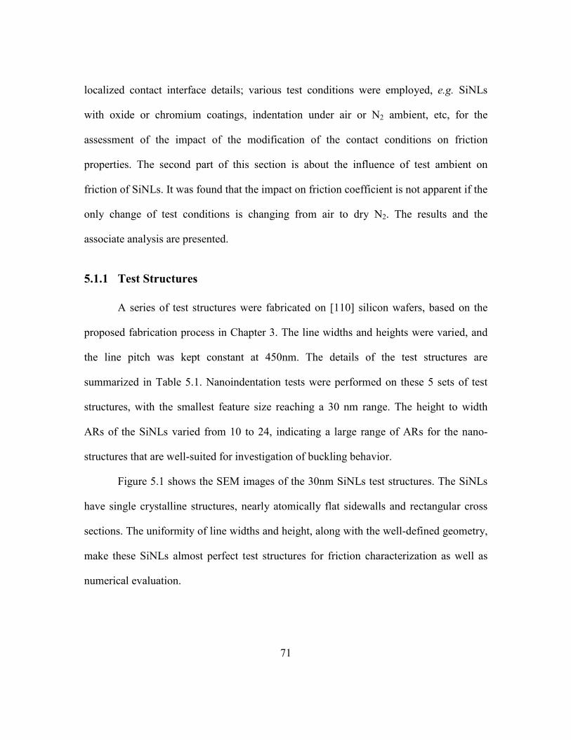
71
localized contact interface details; various test conditions were employed, e.g. SiNLs
with oxide or chromium coatings, indentation under air or N2 ambient, etc, for the
assessment of the impact of the modification of the contact conditions on friction
properties. The second part of this section is about the influence of test ambient on
friction of SiNLs. It was found that the impact on friction coefficient is not apparent if the
only change of test conditions is changing from air to dry N2. The results and the
associate analysis are presented.
5.1.1 Test Structures
A series of test structures were fabricated on [110] silicon wafers, based on the
proposed fabrication process in Chapter 3. The line widths and heights were varied, and
the line pitch was kept constant at 450nm. The details of the test structures are
summarized in Table 5.1. Nanoindentation tests were performed on these 5 sets of test
structures, with the smallest feature size reaching a 30 nm range. The height to width
ARs of the SiNLs varied from 10 to 24, indicating a large range of ARs for the nano-
structures that are well-suited for investigation of buckling behavior.
Figure 5.1 shows the SEM images of the 30nm SiNLs test structures. The SiNLs
have single crystalline structures, nearly atomically flat sidewalls and rectangular cross
sections. The uniformity of line widths and height, along with the well-defined geometry,
make these SiNLs almost perfect test structures for friction characterization as well as
numerical evaluation.
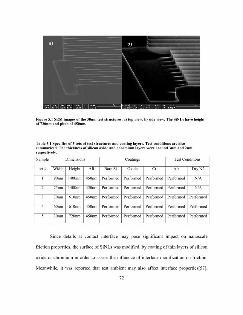
72
Figure 5.1 SEM images of the 30nm test structures. a) top view. b) side view. The SiNLs have height of 720nm and pitch of 450nm.
Table 5.1 Specifics of 5 sets of test structures and coating layers. Test conditions are also summarized. The thickness of silicon oxide and chromium layers were around 3nm and 2nm respectively.
Sample
set #
Dimensions Coatings Test Conditions
Width Height AR Bare Si Oxide Cr Air Dry N2
1 90nm 1400nm 450nm Performed Performed Performed Performed N/A
2 75nm 1400nm 450nm Performed Performed Performed Performed N/A
3 70nm 610nm 450nm Performed Performed Performed Performed Performed
4 60nm 610nm 450nm Performed Performed Performed Performed Performed
5 30nm 720nm 450nm Performed Performed Performed Performed Performed
Since details at contact interface may pose significant impact on nanoscale
friction properties, the surface of SiNLs was modified, by coating of thin layers of silicon
oxide or chromium in order to assess the influence of interface modification on friction.
Meanwhile, it was reported that test ambient may also affect interface properties[57],
a) b)

73
owing to whether there is an existence of water layer between contact interfaces or not.
The experiments performed are summarized in Table 5.1. The impact of test ambient was
investigated at first, by conducting nanoindentation in both N2 and air ambient on a set of
SiNLs with feature size of 70 nm. The associated background and results are discussed in
the following section.
5.1.2 Impact of Test ambient on Friction at contact
At nanoscale, the existence of a layer of water molecules between the indenter
and SiNLs surface may change the contact nature. When a lubricant layer exists, such as
a water intermediate layer, the friction coefficient may be significantly reduced. Without
the water molecules or other intermediate layers, intimate contact normally occurs. To
assess the impact of test ambient on the contact interface modes, Nanoindentation tests
were conducted both in N2 and air ambient. It was noted that at air ambient, the relative
humidity is roughly constant of ~45% RH, while in a dry N2 ambient the humidity is
much lower and is smaller than 5% RH. It is expected under such a low humidity, the
contact friction forces should be larger than that in air ambient, leading to a higher critical
buckling load under indentation test. All the experiments were performed at room
temperature.
The air ambient test condition was just carrying out the experiments in regular lab
environment. The test system was covered by a transparent cover to reduce the influence
of air flow, which is shown in Figure 5.2. The humidity inside the enclosure was
measured to be around 45% RH during of the indentations. In order to achieve a dry
ambient test condition, two steps were needed. The first step was to bake out the trapped
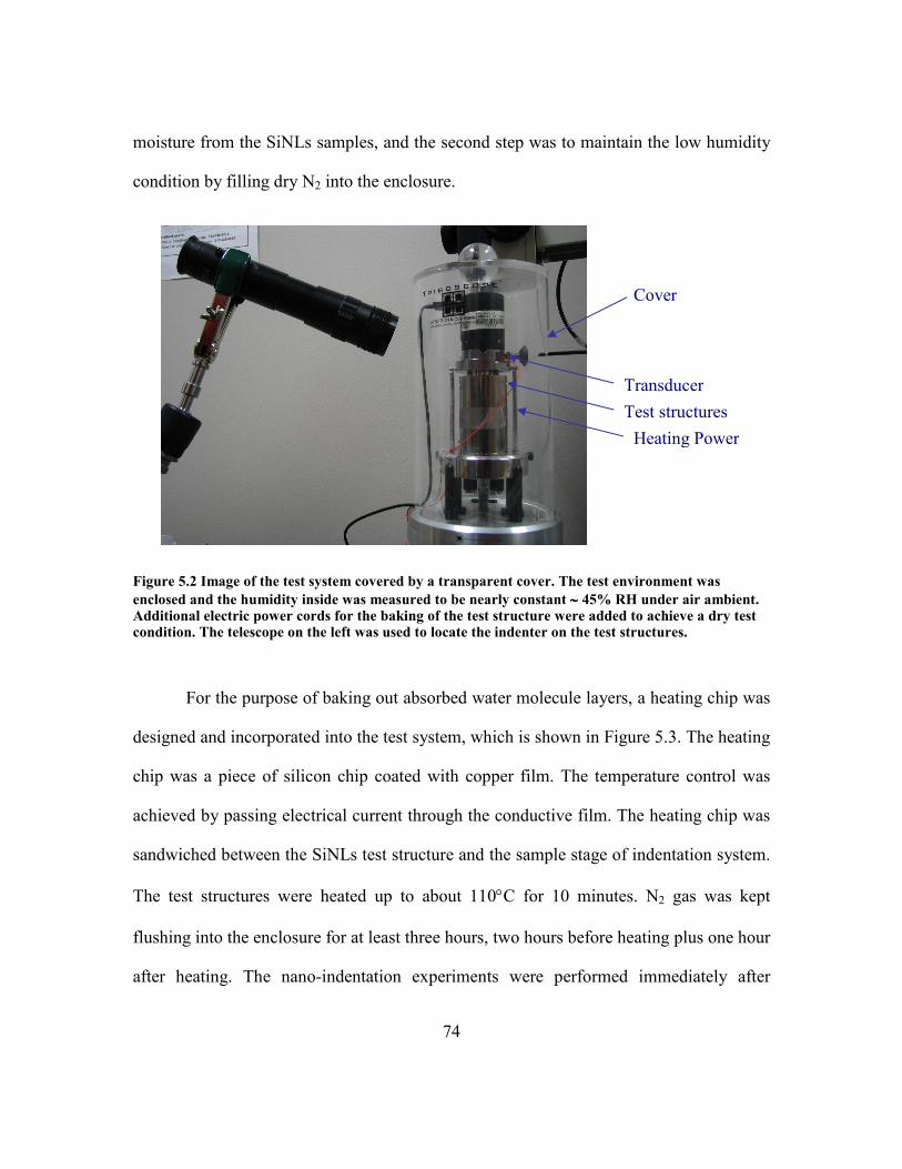
74
moisture from the SiNLs samples, and the second step was to maintain the low humidity
condition by filling dry N2 into the enclosure.
Figure 5.2 Image of the test system covered by a transparent cover. The test environment was enclosed and the humidity inside was measured to be nearly constant ∼∼∼∼ 45% RH under air ambient. Additional electric power cords for the baking of the test structure were added to achieve a dry test condition. The telescope on the left was used to locate the indenter on the test structures.
For the purpose of baking out absorbed water molecule layers, a heating chip was
designed and incorporated into the test system, which is shown in Figure 5.3. The heating
chip was a piece of silicon chip coated with copper film. The temperature control was
achieved by passing electrical current through the conductive film. The heating chip was
sandwiched between the SiNLs test structure and the sample stage of indentation system.
The test structures were heated up to about 110°C for 10 minutes. N2 gas was kept
flushing into the enclosure for at least three hours, two hours before heating plus one hour
after heating. The nano-indentation experiments were performed immediately after
Cover
Transducer
Test structures
Heating Power
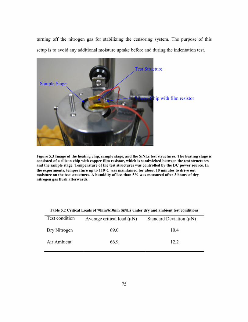
75
turning off the nitrogen gas for stabilizing the censoring system. The purpose of this
setup is to avoid any additional moisture uptake before and during the indentation test.
Figure 5.3 Image of the heating chip, sample stage, and the SiNLs test structures. The heating stage is consisted of a silicon chip with copper film resistor, which is sandwiched between the test structures and the sample stage. Temperature of the test structures was controlled by the DC power source. In the experiments, temperature up to 110°°°°C was maintained for about 10 minutes to drive out moisture on the test structures. A humidity of less than 5% was measured after 3 hours of dry nitrogen gas flush afterwards.
Table 5.2 Critical Loads of 70nm/610nm SiNLs under dry and ambient test conditions
Test condition Average critical load (µN) Standard Deviation (µN)
Dry Nitrogen 69.0 10.4
Air Ambient 66.9 12.2
Sample Stage
Test Structure
Silicon Chip with film resistor
76
Table 5.2 shows the experimental results of nanoindentation on the SiNLs with 70
nm linewidth. Interestingly, it was found that statistically the critical buckling load of
SiNLs did not show significant differences between the two humidity conditions. The
results at the first glance is sort of in contradiction with the contact theory presented in
Chapter 2, which suggested that the water intermediate layer under a humid condition
may change the contact nature and greatly affect the contact friction. However in our
experimental conditions, this is reasonable and it will be addressed in detail next.
As it is mentioned before, the water intermediate layer, particularly under a high
humidity ambient, may serve as a lubricating layer for the contact, thus significantly
reduce the friction force. When there is no intermediate layer existing, intimate contact
may establish and the friction force increases. One possible explanation of our
nanoindentation phenomenon is the effect of high contact pressure.
It was reported that high contact pressure of a few hundreds of MPa will squeeze
out water layers between contacting surfaces. In nanoindentation tests, generally the force
applied on the SiNLs is in the range of 10~200µN. Since the size of the contact zone
should be at the same order of the width of SiNLs, which gives a contact area of ∼10-14m2
, the contact pressure in the nanoindentation test is estimated to be of 10~20 GPa. This
high contact pressure can initiate an intimate contact between the indenter and SiNLs,
even with the existence of a water molecular intermediate layer.
Another perspective to look into this issue, is to understand the boundary
conditions of the water intermediate layer posing effect on the contact friction. In Chapter
77
2 it is shown that the adhesion between the two contact surfaces generates an offset to the
Hertzian force. The offset is in the range of
γπRnFadhesive ~ ,
where n is a number in the range of 1.5~2, and γ is the surface tension of contacting
surface which is normally on the order of 0.1J/m2 for solid-solid contact, and 0.073J/m2
for water. Assuming R is the line width of SiNLs, the offset force is found to be less than
0.1µN. Considering under the condition of the applied indentation force is generally
about 10~200µN, the effect of the adhesion force with a water intermediate layer on the
contact friction is less than 1% here.
From the above analysis, it is concluded that due to a high elastic pressure
between the contact surfaces in the nanoindentation tests, the moisture effect on the
change of contact nature was not likely to be observed in experiments. Nevertheless, it is
also mean that the adhesion force contributes little to the contact area, the friction force,
and the buckling behavior of SiNLs. Thus Hertzian contact model is still a valid
approximation to evaluate the contact area at nano-scale. An analysis model is developed
in the next section, which is based on the Hertzian contact model and the fact that the
effect of adhesion force can be neglected, to deduce penetration depth, contact area, and
the friction shear stress at the nano-contact. The model results will be compared with
experimental results, which are mainly under air ambient test condition.
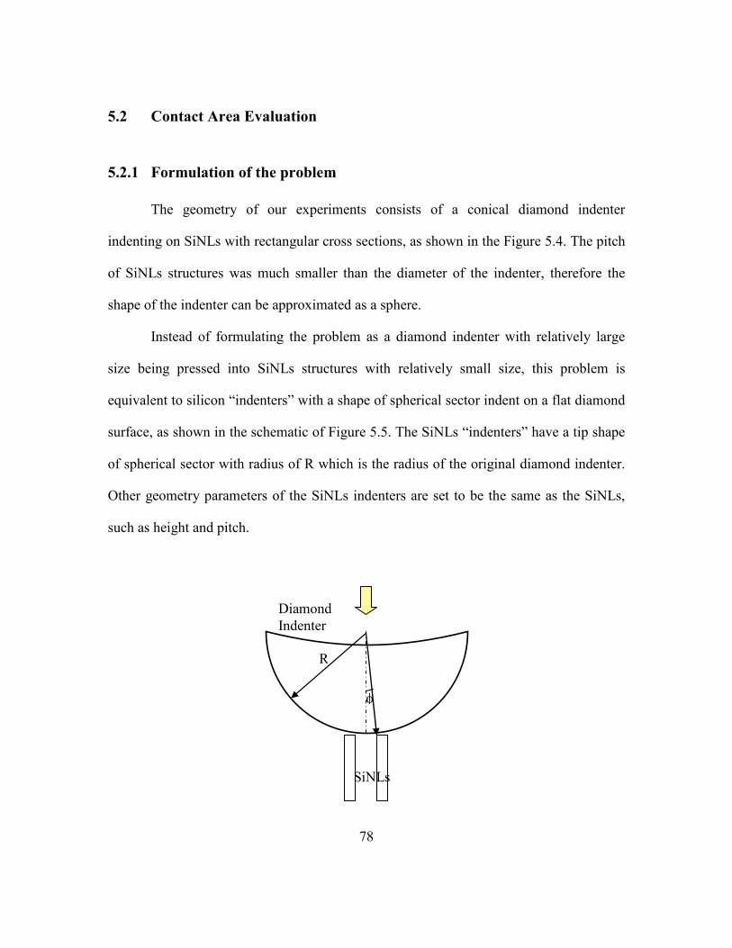
78
5.2 Contact Area Evaluation
5.2.1 Formulation of the problem
The geometry of our experiments consists of a conical diamond indenter
indenting on SiNLs with rectangular cross sections, as shown in the Figure 5.4. The pitch
of SiNLs structures was much smaller than the diameter of the indenter, therefore the
shape of the indenter can be approximated as a sphere.
Instead of formulating the problem as a diamond indenter with relatively large
size being pressed into SiNLs structures with relatively small size, this problem is
equivalent to silicon “indenters” with a shape of spherical sector indent on a flat diamond
surface, as shown in the schematic of Figure 5.5. The SiNLs “indenters” have a tip shape
of spherical sector with radius of R which is the radius of the original diamond indenter.
Other geometry parameters of the SiNLs indenters are set to be the same as the SiNLs,
such as height and pitch.
Diamond Indenter
R
SiNLs
φ
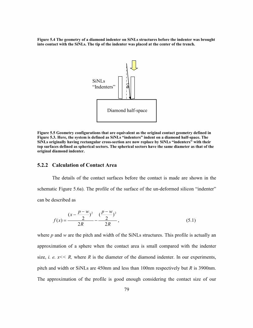
79
Figure 5.4 The geometry of a diamond indenter on SiNLs structures before the indenter was brought into contact with the SiNLs. The tip of the indenter was placed at the center of the trench.
SiNLs “Indenters”
Diamond half-space
φ
Figure 5.5 Geometry configurations that are equivalent as the original contact geometry defined in Figure 5.3. Here, the system is defined as SiNLs “indenters” indent on a diamond half-space. The SiNLs originally having rectangular cross-section are now replace by SiNLs “indenters” with their top surfaces defined as spherical sectors. The spherical sectors have the same diameter as that of the original diamond indenter.
5.2.2 Calculation of Contact Area
The details of the contact surfaces before the contact is made are shown in the
schematic Figure 5.6a). The profile of the surface of the un-deformed silicon “indenter”
can be described as
R
wp
R
wpx
xf2
)2
(
2
)2
()(
22 −
−
−−
= , (5.1)
where p and w are the pitch and width of the SiNLs structures. This profile is actually an
approximation of a sphere when the contact area is small compared with the indenter
size, i. e. x<< R, where R is the diameter of the diamond indenter. In our experiments,
pitch and width or SiNLs are 450nm and less than 100nm respectively but R is 3900nm.
The approximation of the profile is good enough considering the contact size of our
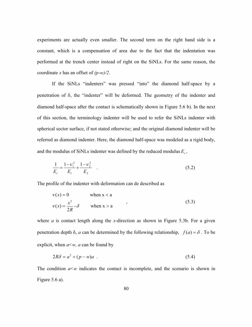
80
experiments are actually even smaller. The second term on the right hand side is a
constant, which is a compensation of area due to the fact that the indentation was
performed at the trench center instead of right on the SiNLs. For the same reason, the
coordinate x has an offset of (p-w)/2.
If the SiNLs “indenters” was pressed “into” the diamond half-space by a
penetration of δ, the “indenter” will be deformed. The geometry of the indenter and
diamond half-space after the contact is schematically shown in Figure 5.6 b). In the next
of this section, the terminology indenter will be used to refer the SiNLs indenter with
spherical sector surface, if not stated otherwise; and the original diamond indenter will be
referred as diamond indenter. Here, the diamond half-space was modeled as a rigid body,
and the modulus of SiNLs indenter was defined by the reduced modulus rE ,
2
22
1
21 111
EEEr
νν −+
−= . (5.2)
The profile of the indenter with deformation can de described as
ahen x w- 2
)(
a when x 0)(2
>=
<=
δν
ν
Rx
x
x , (5.3)
where a is contact length along the x-direction as shown in Figure 5.3b. For a given
penetration depth δ, a can be determined by the following relationship, δ=)(af . To be
explicit, when a<w, a can be found by
awpaR )(2 2 −+=δ . (5.4)
The condition a<w indicates the contact is incomplete, and the scenario is shown in
Figure 5.6 a).
81
With the increase of the applied force, the contact area also increases. When a=w,
the contact becomes complete, then the contact length along line width direction a is
constant. However, the contact length along line length direction, which is denoted as b,
changes as the penetration depth changes. The relation between b and δ is
δRb 2= . (5.5)
In both cases, the area of contact is calculated as
)2
()2
(1)2
arcsin()2
()2
(1)2
arcsin(
)2
()2
(1)2
arcsin(2
222
22
=
−−−−
−−
++−+
+
<
−−−−
−−
=
w)(acwp
cwp
cwp
cwp
cwp
cwp
c
w)(acwp
cwp
cwp
c
A
π, (5.6)
where
)
2(
2
22
=+−
<+=
w)(abwp
w)(aap-w
c . (5.7)
Therefore, once the penetration depth δ is determined, the parameters of contact
length a or b can be calculated by equations 5.4 and 5.5, respectively. Then the contact
area can be calculated according to equation 5.7.
However, the challenge is that the penetration depth δ is not a quantity that is
directly measured or monitored by experiments. To address this issue, there are two
possible methods tackling this problem. The first method is to calculate δ from the
displacements of indenter that were experimentally measured by the displacement
transducer. The second method is to calculate δ from the indentation forces. The
82
following sections will discuss the evaluation of penetration depth δ using these two
methods, respectively.
5.2.3 Calculation of Penetration Depth by indentation Displacement
The displacement of indenter consists of the local deformation of SiNL
(penetration depth δ) and the elastic deformation of the SiNL under compressive force. A
simple model is used to express the relation between displacement and penetration depth
elasticdd += δ , (5.8)
where d is the experimentally measured displacement of indenter. d is around 10 nm to
20 nm before buckling of SiNLs. elasticd is the global deformation of the SiNL when it is
subjected to compressive forces. It is noted that only localized deformation at the contact,
which represents the penetration depth of indenter, contributes to the contact area
estimation.
It is difficult to derive an analytical solution for elasticd , since the compression
stress on the SiNLs was not uniform, and the deformation of SiNLs is also subjected to
the confinement in the y-direction. FEM simulation was employed to get an approximate
solution of elasticd as a function of applied forces. A schematic of the FEM model is
shown in Figure 5.7 a) where two key points were defined as A and B. Point A was on
the upper-left corner of the SiNL, and Point B was on the sidewall of SiNL with a
distance of 50 nm below point A. In the indentation, SiNL was only subjected to
compressive global elastic deformation at OB; and the localized deformation only
occurred at BA. These assumptions were based on the fact that the total deformation
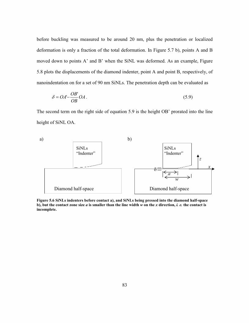
83
before buckling was measured to be around 20 nm, plus the penetration or localized
deformation is only a fraction of the total deformation. In Figure 5.7 b), points A and B
moved down to points A’ and B’ when the SiNL was deformed. As an example, Figure
5.8 plots the displacements of the diamond indenter, point A and point B, respectively, of
nanoindentation on for a set of 90 nm SiNLs. The penetration depth can be evaluated as
OAOBOB
OA'
'−=δ . (5.9)
The second term on the right side of equation 5.9 is the height OB’ prorated into the line
height of SiNL OA.
Figure 5.6 SiNLs indenters before contact a), and SiNLs being pressed into the diamond half-space b), but the contact zone size a is smaller than the line width w on the x direction, i. e. the contact is incomplete.
Diamond half-space Diamond half-space
a) b)
SiNLs “Indenter”
SiNLs “Indenter”
δ x a
w
z
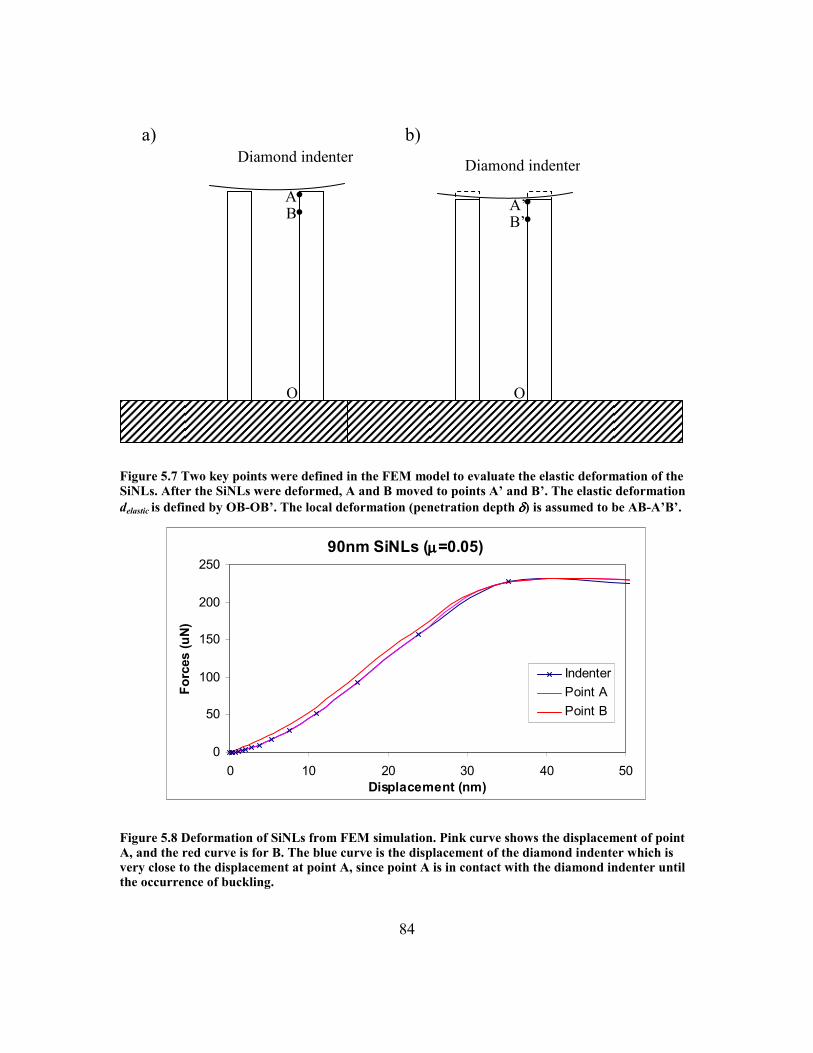
84
Figure 5.7 Two key points were defined in the FEM model to evaluate the elastic deformation of the SiNLs. After the SiNLs were deformed, A and B moved to points A’ and B’. The elastic deformation delastic is defined by OB-OB’. The local deformation (penetration depth δδδδ) is assumed to be AB-A’B’.
90nm SiNLs (µµµµ=0.05)
0
50
100
150
200
250
0 10 20 30 40 50Displacement (nm)
Forces (uN)
IndenterPoint APoint B
Figure 5.8 Deformation of SiNLs from FEM simulation. Pink curve shows the displacement of point A, and the red curve is for B. The blue curve is the displacement of the diamond indenter which is very close to the displacement at point A, since point A is in contact with the diamond indenter until the occurrence of buckling.
Diamond indenter
B A
Diamond indenter
B’ A’
O O
• •
• •
b) a)
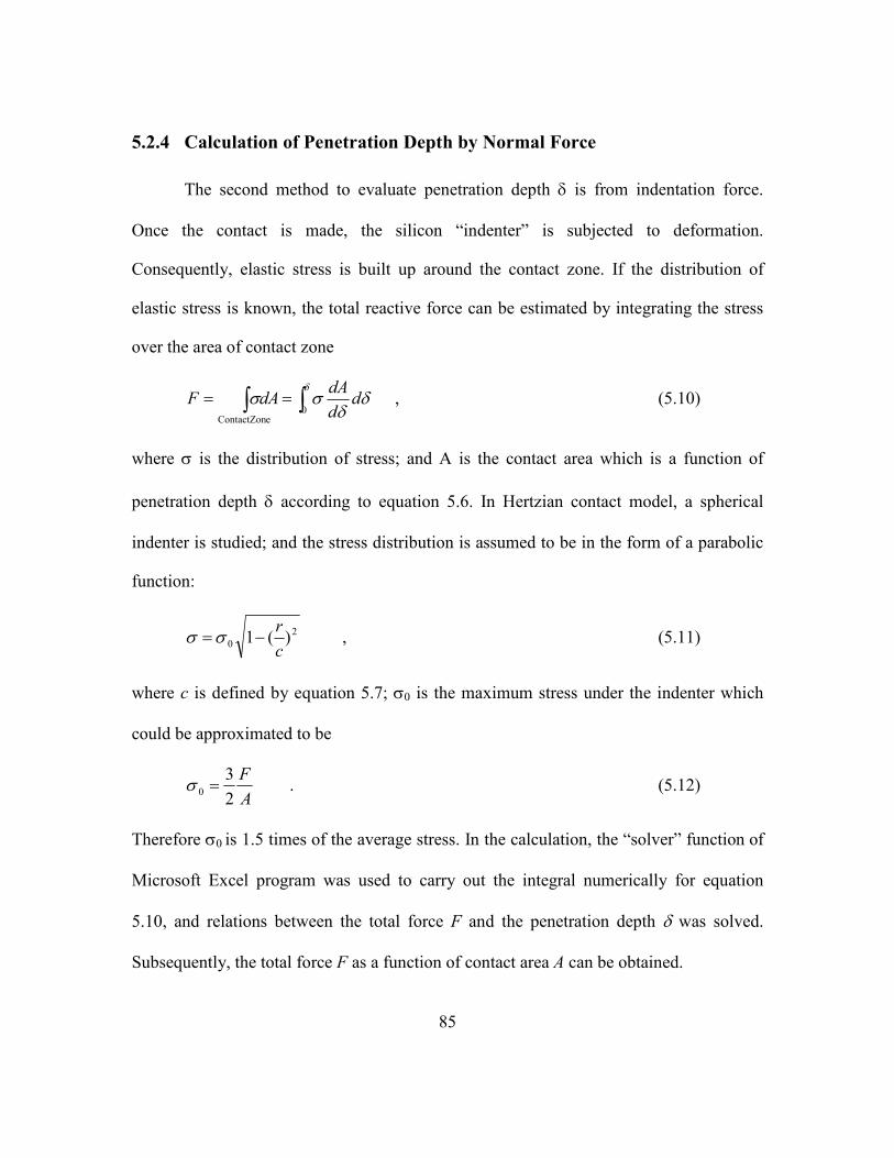
85
5.2.4 Calculation of Penetration Depth by Normal Force
The second method to evaluate penetration depth δ is from indentation force.
Once the contact is made, the silicon “indenter” is subjected to deformation.
Consequently, elastic stress is built up around the contact zone. If the distribution of
elastic stress is known, the total reactive force can be estimated by integrating the stress
over the area of contact zone
∫∫ ==δ
δδ
σσ0
eContactZon
dddA
dAF , (5.10)
where σ is the distribution of stress; and A is the contact area which is a function of
penetration depth δ according to equation 5.6. In Hertzian contact model, a spherical
indenter is studied; and the stress distribution is assumed to be in the form of a parabolic
function:
20 )(1
cr
−= σσ , (5.11)
where c is defined by equation 5.7; σ0 is the maximum stress under the indenter which
could be approximated to be
AF
23
0 =σ . (5.12)
Therefore σ0 is 1.5 times of the average stress. In the calculation, the “solver” function of
Microsoft Excel program was used to carry out the integral numerically for equation
5.10, and relations between the total force F and the penetration depth δ was solved.
Subsequently, the total force F as a function of contact area A can be obtained.
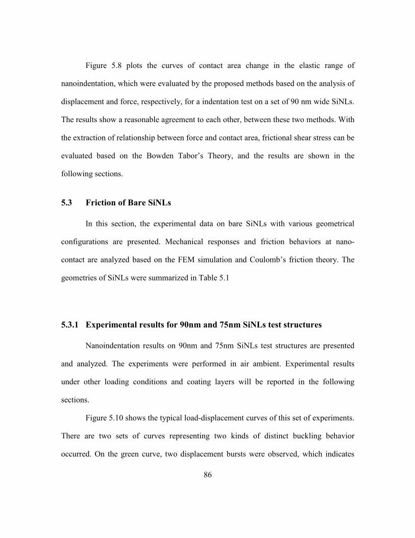
86
Figure 5.8 plots the curves of contact area change in the elastic range of
nanoindentation, which were evaluated by the proposed methods based on the analysis of
displacement and force, respectively, for a indentation test on a set of 90 nm wide SiNLs.
The results show a reasonable agreement to each other, between these two methods. With
the extraction of relationship between force and contact area, frictional shear stress can be
evaluated based on the Bowden Tabor’s Theory, and the results are shown in the
following sections.
5.3 Friction of Bare SiNLs
In this section, the experimental data on bare SiNLs with various geometrical
configurations are presented. Mechanical responses and friction behaviors at nano-
contact are analyzed based on the FEM simulation and Coulomb’s friction theory. The
geometries of SiNLs were summarized in Table 5.1
5.3.1 Experimental results for 90nm and 75nm SiNLs test structures
Nanoindentation results on 90nm and 75nm SiNLs test structures are presented
and analyzed. The experiments were performed in air ambient. Experimental results
under other loading conditions and coating layers will be reported in the following
sections.
Figure 5.10 shows the typical load-displacement curves of this set of experiments.
There are two sets of curves representing two kinds of distinct buckling behavior
occurred. On the green curve, two displacement bursts were observed, which indicates
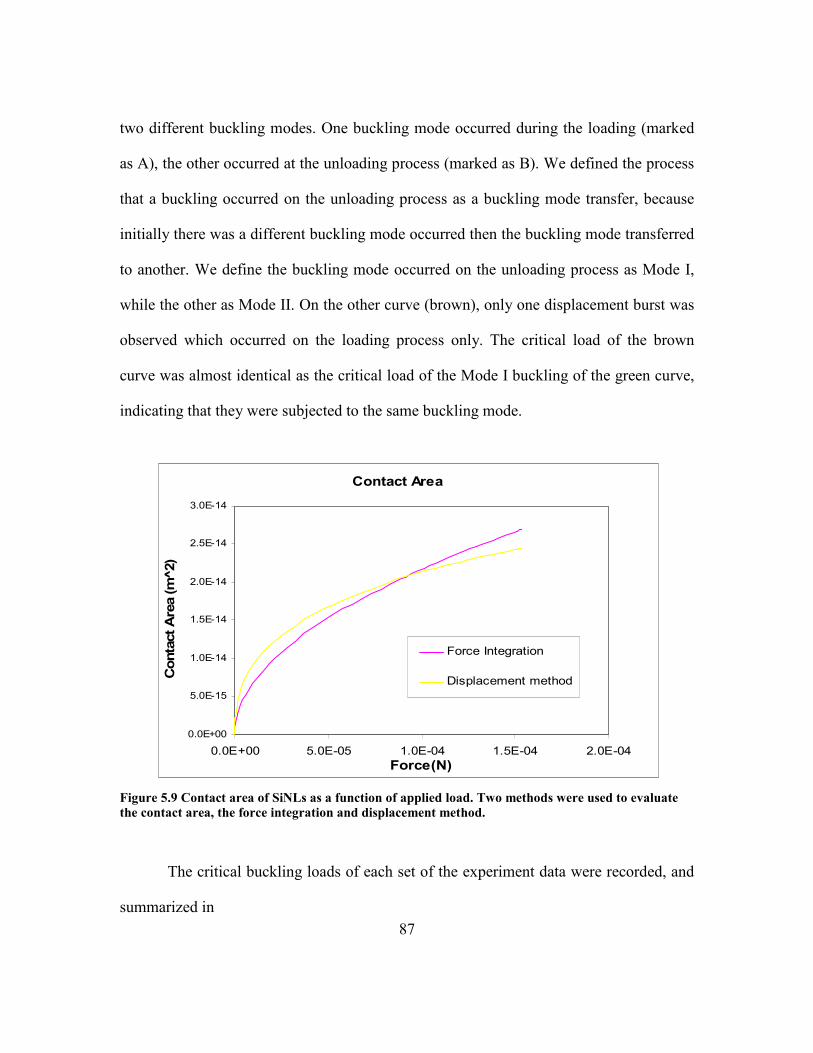
87
two different buckling modes. One buckling mode occurred during the loading (marked
as A), the other occurred at the unloading process (marked as B). We defined the process
that a buckling occurred on the unloading process as a buckling mode transfer, because
initially there was a different buckling mode occurred then the buckling mode transferred
to another. We define the buckling mode occurred on the unloading process as Mode I,
while the other as Mode II. On the other curve (brown), only one displacement burst was
observed which occurred on the loading process only. The critical load of the brown
curve was almost identical as the critical load of the Mode I buckling of the green curve,
indicating that they were subjected to the same buckling mode.
Figure 5.9 Contact area of SiNLs as a function of applied load. Two methods were used to evaluate the contact area, the force integration and displacement method.
The critical buckling loads of each set of the experiment data were recorded, and
summarized in
Contact Area
0.0E+00
5.0E-15
1.0E-14
1.5E-14
2.0E-14
2.5E-14
3.0E-14
0.0E+00 5.0E-05 1.0E-04 1.5E-04 2.0E-04Force(N)
Contact Area (m^2)
Force Integration
Displacement method
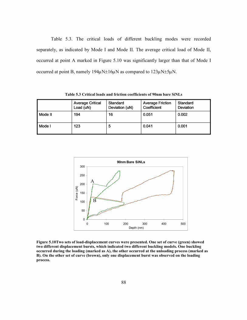
88
Table 5.3. The critical loads of different buckling modes were recorded
separately, as indicated by Mode I and Mode II. The average critical load of Mode II,
occurred at point A marked in Figure 5.10 was significantly larger than that of Mode I
occurred at point B, namely 194µN±16µN as compared to 123µN±5µN.
Table 5.3 Critical loads and friction coefficients of 90nm bare SiNLs
90nm Bare SiNLs
0
50
100
150
200
250
300
0 100 200 300 400 500Depth (nm)
Force (uN
)
Figure 5.10Two sets of load-displacement curves were presented. One set of curve (green) showed two different displacement bursts, which indicated two different buckling models. One buckling occurred during the loading (marked as A), the other occurred at the unloading process (marked as B). On the other set of curve (brown), only one displacement burst was observed on the loading process.
5
16
Standard Deviation (uN)
0.041
0.051
Average Friction Coefficient
123
194
Average Critical Load (uN)
Standard Deviation
0.001Mode I
0.002Mode II
5
16
Standard Deviation (uN)
0.041
0.051
Average Friction Coefficient
123
194
Average Critical Load (uN)
Standard Deviation
0.001Mode I
0.002Mode II
A
B
89
The friction coefficients µ were determined based on FEM simulation by
comparing the critical loads of simulated load-displacement curve and experimental load-
displacement curve. The friction coefficients results were also summarized in
Table 5.3. The Mode II buckling mode yielded an average friction coefficient of
0.051 which is slightly larger than that of Mode I buckling mode at 0.041.
Next the frictional shear stress will be evaluated. In Chapter 1, the frictional shear
stress τ was defined as
AF f τ= ,
where the contact area is evaluated in Section 2. The friction force Ff can be calculated
according to the geometry and Equation 4.4,
2cos2sincosFF
F f θµ
θµθµ
≈+
= .
Therefore the frictional shear stress is
2cosF
AA
F f
θµτ == ,
where F is the experimentally measured critical buckling load. The frictional shear stress
data are summarized in Table 5.4. The data show that the difference between shear
stresses of Mode I and Mode II buckling is significant. In the case when there is a
buckling mode transition, the initial buckling is Mode II buckling with high frictional
shear stress but after experiencing the postbuckling loading process, a Mode I buckling
occurs during the unloading process. The frictional shear stress reduced significantly in
this process, indicating the contact history had a significant effect on friction. The contact
90
history effect is confirmed by nanoindentation experiments under cyclic loading which
will be discussed in Section 5.
Table 5.4 Frictional Shear Stress of 90nm SiNLs
Average
Critical
Load(µN)
Average
Friction
Coefficient
Contact Area
(10-14 m2)
Average Shear Stress
(MPa)
Force
method
Disp
method
Force
method
Disp
method
Mode II 194 0.051 2.2 2.17 225 228
Mode I 123 0.041 1.83 1.72 138 147
The buckling behavior for the 75nm SiNLs test structures was similar to the 90nm
test structure. A buckling mode transition from Mode II to Mode I was observed in the
nanoindentation experiments. The friction coefficient and frictional shear stress results
are summarized in Table 5.5. Similarly, the Mode II buckling is due to high shear stress.
Table 5.5Frictional Shear Stress of 75nm SiNLs
Average
Critical
Load(µN)
Average
Friction
Coefficient
Contact Area
(10-14 m2)
Average Shear Stress
(MPa)
Force
method
Disp
method
Force
method
Disp
method
Mode II 95 0.049 0.89 0.81 285 265
Mode I 64 0.041 1.12 0.95 138 117
91
5.3.2 Experimental results for 60nm/610nm and 30nm/720nm SiNLs
The same experimental protocols were repeated on SiNLs test structures of
60nm/610nm, and 30nm/720nm. Besides the difference of line widths, these two sets of
test structures have different heights compared to test structures of 90nm/1400nm and
75nm/1400nm. According to analysis in Chapter 4, the chance to observe Mode II
buckling for the 60nm test structures is much less because of the small aspect ratio. This
is agreed by the experimental observation. However, models in Chapter 4 predicted a
buckling mode transition for the 30nm test structures because they have the largest aspect
ratio among all test structures. In experiments no significant buckling mode transition
was observed. This may suggest that the friction force is not strong enough to initiate
Mode II buckling, although the aspect ratio is larger. All the critical loads and friction
coefficients are summarized in Table 5.6 and Figure 5.11 for bare SiNLs. Figure 5.12
shows the corresponding frictional shear stress. Some typical load-displacement curves
are shown in Figure 5.13 and Figure 5.14.
It is interesting to note that the variations of critical loads and friction coefficients
of the 30nm/720nm test structures were very large compared to other sets of test
structures. Although the transfer of buckling modes was not observed, some of the
friction coefficients were as large as 0.05 which is close to the average of friction
coefficients of the Mode II buckling for the 90nm/1400nm and 75nm/1400nm test
structures. For those buckling with large friction coefficients, Mode II buckling might
have occurred as well, except that Mode I buckling did not occur during the unloading
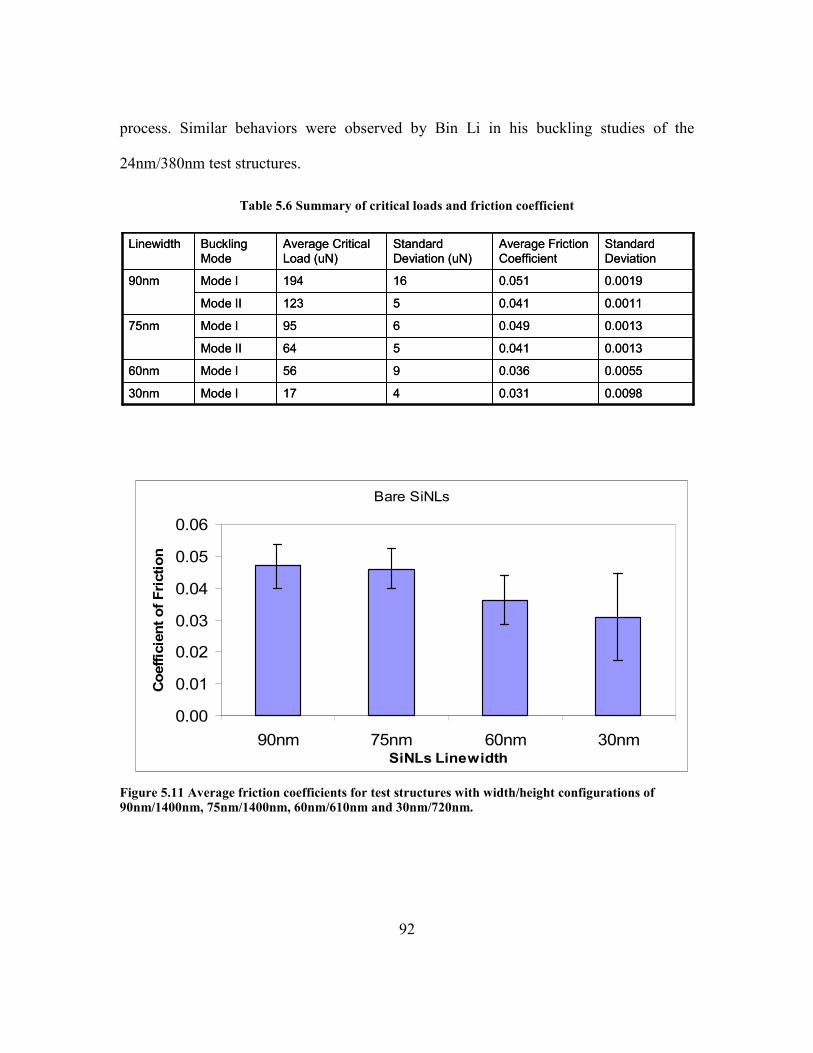
92
process. Similar behaviors were observed by Bin Li in his buckling studies of the
24nm/380nm test structures.
Table 5.6 Summary of critical loads and friction coefficient
Figure 5.11 Average friction coefficients for test structures with width/height configurations of 90nm/1400nm, 75nm/1400nm, 60nm/610nm and 30nm/720nm.
0.00550.036956Mode I60nm
0.00110.0415123Mode II
0.00130.049695Mode I75nm
0.00190.05116194Mode I90nm
0.00130.041564Mode II
30nm
Linewidth
4
Standard Deviation (uN)
0.031
Average Friction Coefficient
17
Average Critical Load (uN)
Standard Deviation
Buckling Mode
0.0098Mode I
0.00550.036956Mode I60nm
0.00110.0415123Mode II
0.00130.049695Mode I75nm
0.00190.05116194Mode I90nm
0.00130.041564Mode II
30nm
Linewidth
4
Standard Deviation (uN)
0.031
Average Friction Coefficient
17
Average Critical Load (uN)
Standard Deviation
Buckling Mode
0.0098Mode I
Bare SiNLs
0.00
0.01
0.02
0.03
0.04
0.05
0.06
90nm 75nm 60nm 30nmSiNLs Linewidth
Coefficient of Friction Bare SiNLs
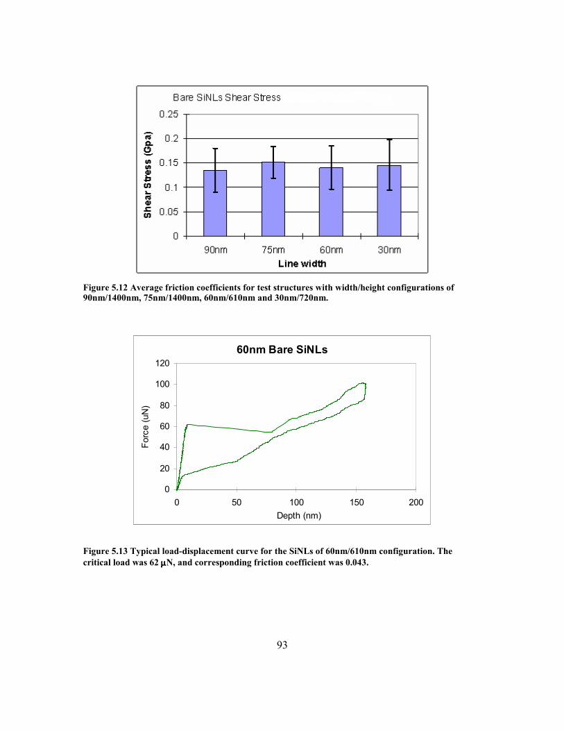
93
Figure 5.12 Average friction coefficients for test structures with width/height configurations of 90nm/1400nm, 75nm/1400nm, 60nm/610nm and 30nm/720nm.
60nm Bare SiNLs
0
20
40
60
80
100
120
0 50 100 150 200Depth (nm)
Force (uN
)
Figure 5.13 Typical load-displacement curve for the SiNLs of 60nm/610nm configuration. The critical load was 62 µµµµN, and corresponding friction coefficient was 0.043.
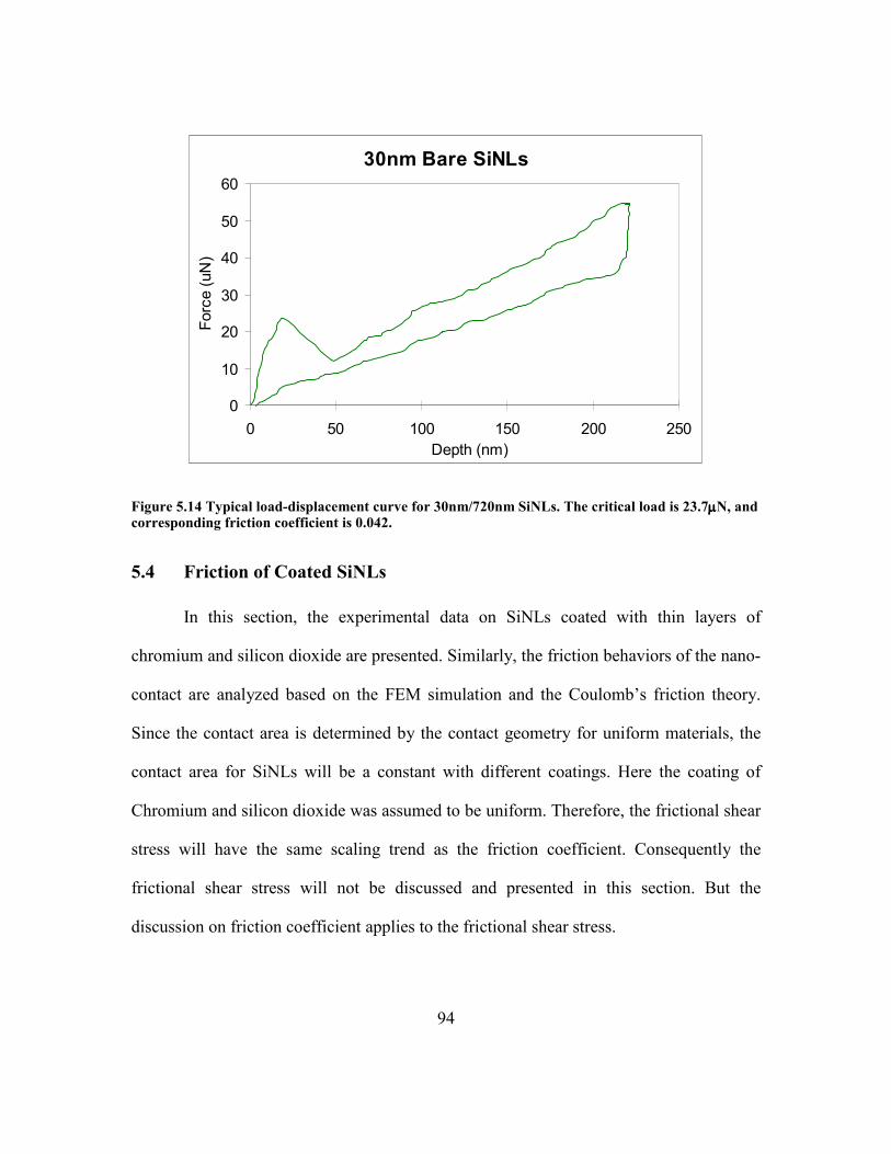
94
30nm Bare SiNLs
0
10
20
30
40
50
60
0 50 100 150 200 250Depth (nm)
Force (uN)
Figure 5.14 Typical load-displacement curve for 30nm/720nm SiNLs. The critical load is 23.7µµµµN, and corresponding friction coefficient is 0.042.
5.4 Friction of Coated SiNLs
In this section, the experimental data on SiNLs coated with thin layers of
chromium and silicon dioxide are presented. Similarly, the friction behaviors of the nano-
contact are analyzed based on the FEM simulation and the Coulomb’s friction theory.
Since the contact area is determined by the contact geometry for uniform materials, the
contact area for SiNLs will be a constant with different coatings. Here the coating of
Chromium and silicon dioxide was assumed to be uniform. Therefore, the frictional shear
stress will have the same scaling trend as the friction coefficient. Consequently the
frictional shear stress will not be discussed and presented in this section. But the
discussion on friction coefficient applies to the frictional shear stress.
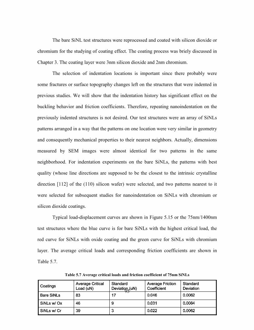
95
The bare SiNL test structures were reprocessed and coated with silicon dioxide or
chromium for the studying of coating effect. The coating process was briely discussed in
Chapter 3. The coating layer were 3nm silicon dioxide and 2nm chromium.
The selection of indentation locations is important since there probably were
some fractures or surface topography changes left on the structures that were indented in
previous studies. We will show that the indentation history has significant effect on the
buckling behavior and friction coefficients. Therefore, repeating nanoindentation on the
previously indented structures is not desired. Our test structures were an array of SiNLs
patterns arranged in a way that the patterns on one location were very similar in geometry
and consequently mechanical properties to their nearest neighbors. Actually, dimensions
measured by SEM images were almost identical for two patterns in the same
neighborhood. For indentation experiments on the bare SiNLs, the patterns with best
quality (whose line directions are supposed to be the closest to the intrinsic crystalline
direction [112] of the (110) silicon wafer) were selected, and two patterns nearest to it
were selected for subsequent studies for nanoindentation on SiNLs with chromium or
silicon dioxide coatings.
Typical load-displacement curves are shown in Figure 5.15 or the 75nm/1400nm
test structures where the blue curve is for bare SiNLs with the highest critical load, the
red curve for SiNLs with oxide coating and the green curve for SiNLs with chromium
layer. The average critical loads and corresponding friction coefficients are shown in
Table 5.7.
Table 5.7 Average critical loads and friction coefficient of 75nm SiNLs �����������1783Bare SiNLs �����������946SiNLs w/ Ox �Standard Deviation (uN) �����Average Friction
Coefficient��Average Critical Load (uN)Standard Deviation
Coatings ������SiNLs w/ Cr
�����������1783Bare SiNLs �����������946SiNLs w/ Ox �Standard Deviation (uN) �����Average Friction
Coefficient��Average Critical Load (uN)Standard Deviation
Coatings ������SiNLs w/ Cr
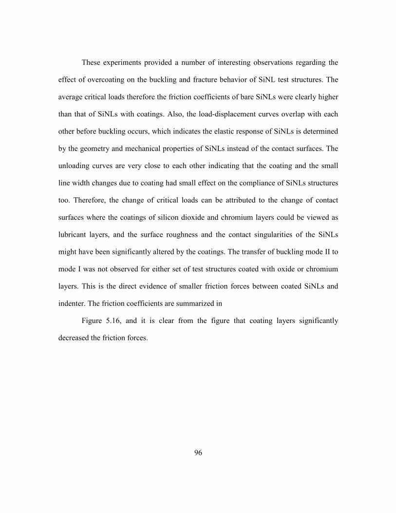
96
These experiments provided a number of interesting observations regarding the
effect of overcoating on the buckling and fracture behavior of SiNL test structures. The
average critical loads therefore the friction coefficients of bare SiNLs were clearly higher
than that of SiNLs with coatings. Also, the load-displacement curves overlap with each
other before buckling occurs, which indicates the elastic response of SiNLs is determined
by the geometry and mechanical properties of SiNLs instead of the contact surfaces. The
unloading curves are very close to each other indicating that the coating and the small
line width changes due to coating had small effect on the compliance of SiNLs structures
too. Therefore, the change of critical loads can be attributed to the change of contact
surfaces where the coatings of silicon dioxide and chromium layers could be viewed as
lubricant layers, and the surface roughness and the contact singularities of the SiNLs
might have been significantly altered by the coatings. The transfer of buckling mode II to
mode I was not observed for either set of test structures coated with oxide or chromium
layers. This is the direct evidence of smaller friction forces between coated SiNLs and
indenter. The friction coefficients are summarized in
Figure 5.16, and it is clear from the figure that coating layers significantly
decreased the friction forces.
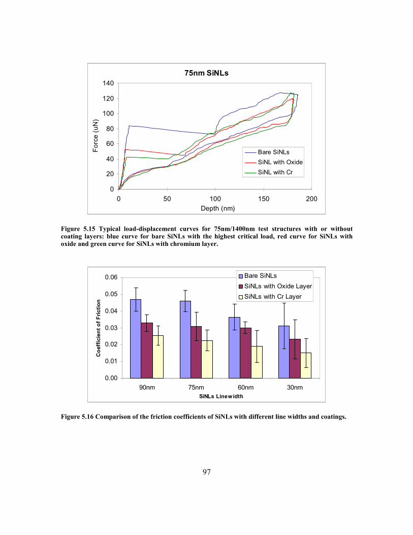
97
75nm SiNLs
0
20
40
60
80
100
120
140
0 50 100 150 200Depth (nm)
Force (uN
)
Bare SiNLs
SiNL with Oxide
SiNL with Cr
Figure 5.15 Typical load-displacement curves for 75nm/1400nm test structures with or without coating layers: blue curve for bare SiNLs with the highest critical load, red curve for SiNLs with oxide and green curve for SiNLs with chromium layer.
0.00
0.01
0.02
0.03
0.04
0.05
0.06
90nm 75nm 60nm 30nmSiNLs Linewidth
Coefficien
t of Friction
Bare SiNLs
SiNLs with Oxide Layer
SiNLs with Cr Layer
Figure 5.16 Comparison of the friction coefficients of SiNLs with different line widths and coatings.
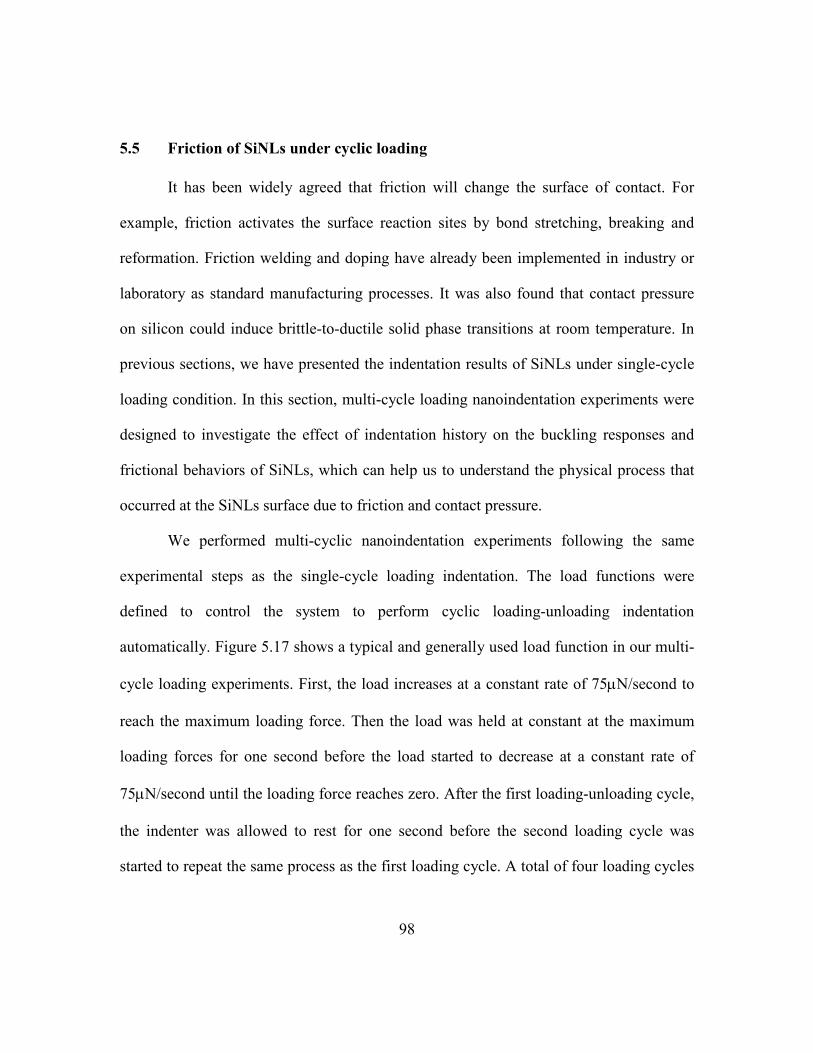
98
5.5 Friction of SiNLs under cyclic loading
It has been widely agreed that friction will change the surface of contact. For
example, friction activates the surface reaction sites by bond stretching, breaking and
reformation. Friction welding and doping have already been implemented in industry or
laboratory as standard manufacturing processes. It was also found that contact pressure
on silicon could induce brittle-to-ductile solid phase transitions at room temperature. In
previous sections, we have presented the indentation results of SiNLs under single-cycle
loading condition. In this section, multi-cycle loading nanoindentation experiments were
designed to investigate the effect of indentation history on the buckling responses and
frictional behaviors of SiNLs, which can help us to understand the physical process that
occurred at the SiNLs surface due to friction and contact pressure.
We performed multi-cyclic nanoindentation experiments following the same
experimental steps as the single-cycle loading indentation. The load functions were
defined to control the system to perform cyclic loading-unloading indentation
automatically. Figure 5.17 shows a typical and generally used load function in our multi-
cycle loading experiments. First, the load increases at a constant rate of 75µN/second to
reach the maximum loading force. Then the load was held at constant at the maximum
loading forces for one second before the load started to decrease at a constant rate of
75µN/second until the loading force reaches zero. After the first loading-unloading cycle,
the indenter was allowed to rest for one second before the second loading cycle was
started to repeat the same process as the first loading cycle. A total of four loading cycles
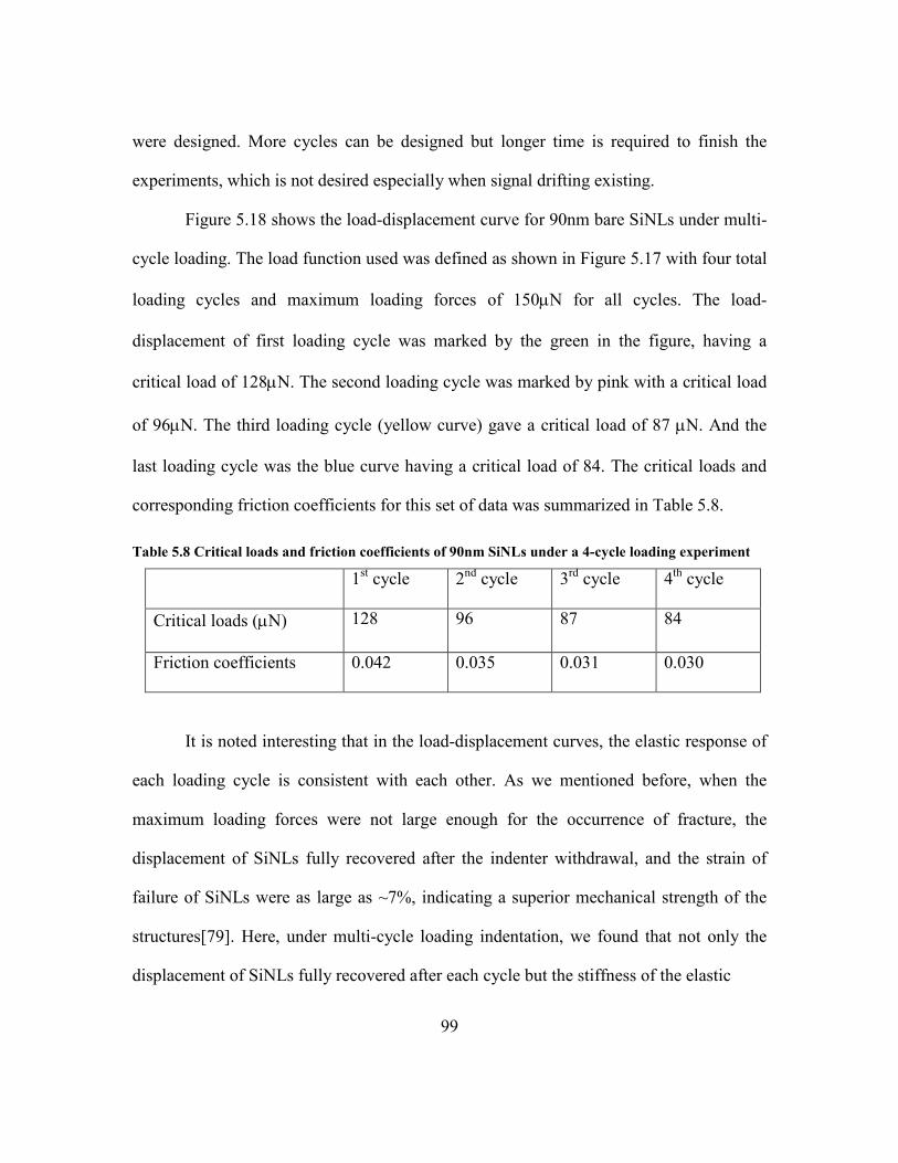
99
were designed. More cycles can be designed but longer time is required to finish the
experiments, which is not desired especially when signal drifting existing.
Figure 5.18 shows the load-displacement curve for 90nm bare SiNLs under multi-
cycle loading. The load function used was defined as shown in Figure 5.17 with four total
loading cycles and maximum loading forces of 150µN for all cycles. The load-
displacement of first loading cycle was marked by the green in the figure, having a
critical load of 128µN. The second loading cycle was marked by pink with a critical load
of 96µN. The third loading cycle (yellow curve) gave a critical load of 87 µN. And the
last loading cycle was the blue curve having a critical load of 84. The critical loads and
corresponding friction coefficients for this set of data was summarized in Table 5.8.
Table 5.8 Critical loads and friction coefficients of 90nm SiNLs under a 4-cycle loading experiment
1st cycle 2nd cycle 3rd cycle 4th cycle
Critical loads (µN) 128 96 87 84
Friction coefficients 0.042 0.035 0.031 0.030
It is noted interesting that in the load-displacement curves, the elastic response of
each loading cycle is consistent with each other. As we mentioned before, when the
maximum loading forces were not large enough for the occurrence of fracture, the
displacement of SiNLs fully recovered after the indenter withdrawal, and the strain of
failure of SiNLs were as large as ~7%, indicating a superior mechanical strength of the
structures[79]. Here, under multi-cycle loading indentation, we found that not only the
displacement of SiNLs fully recovered after each cycle but the stiffness of the elastic
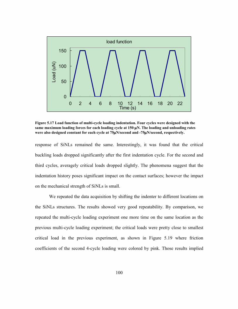
100
load function
0
50
100
150
0 2 4 6 8 10 12 14 16 18 20 22Time (s)
Load
(uN)
Figure 5.17 Load function of multi-cycle loading indentation. Four cycles were designed with the same maximum loading forces for each loading cycle at 150 µµµµN. The loading and unloading rates were also designed constant for each cycle at 75µµµµN/second and -75µµµµN/second, respectively.
response of SiNLs remained the same. Interestingly, it was found that the critical
buckling loads dropped significantly after the first indentation cycle. For the second and
third cycles, averagely critical loads dropped slightly. The phenomena suggest that the
indentation history poses significant impact on the contact surfaces; however the impact
on the mechanical strength of SiNLs is small.
We repeated the data acquisition by shifting the indenter to different locations on
the SiNLs structures. The results showed very good repeatability. By comparison, we
repeated the multi-cycle loading experiment one more time on the same location as the
previous multi-cycle loading experiment; the critical loads were pretty close to smallest
critical load in the previous experiment, as shown in Figure 5.19 where friction
coefficients of the second 4-cycle loading were colored by pink. Those results implied
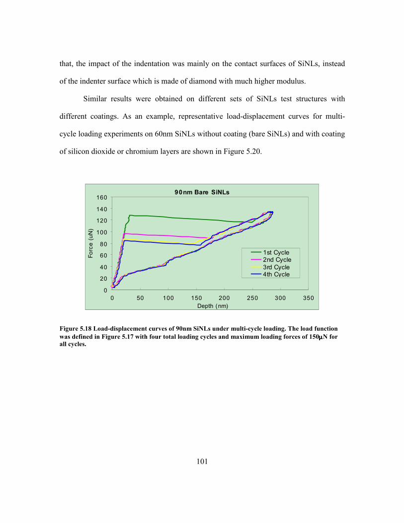
101
that, the impact of the indentation was mainly on the contact surfaces of SiNLs, instead
of the indenter surface which is made of diamond with much higher modulus.
Similar results were obtained on different sets of SiNLs test structures with
different coatings. As an example, representative load-displacement curves for multi-
cycle loading experiments on 60nm SiNLs without coating (bare SiNLs) and with coating
of silicon dioxide or chromium layers are shown in Figure 5.20.
90nm Bare SiNLs
0
20
40
60
80
100
120
140
160
0 50 100 150 200 250 300 350Depth (nm)
Force (uN)
1st Cycle2nd Cycle3rd Cycle4th Cycle
Figure 5.18 Load-displacement curves of 90nm SiNLs under multi-cycle loading. The load function was defined in Figure 5.17 with four total loading cycles and maximum loading forces of 150µµµµN for all cycles.
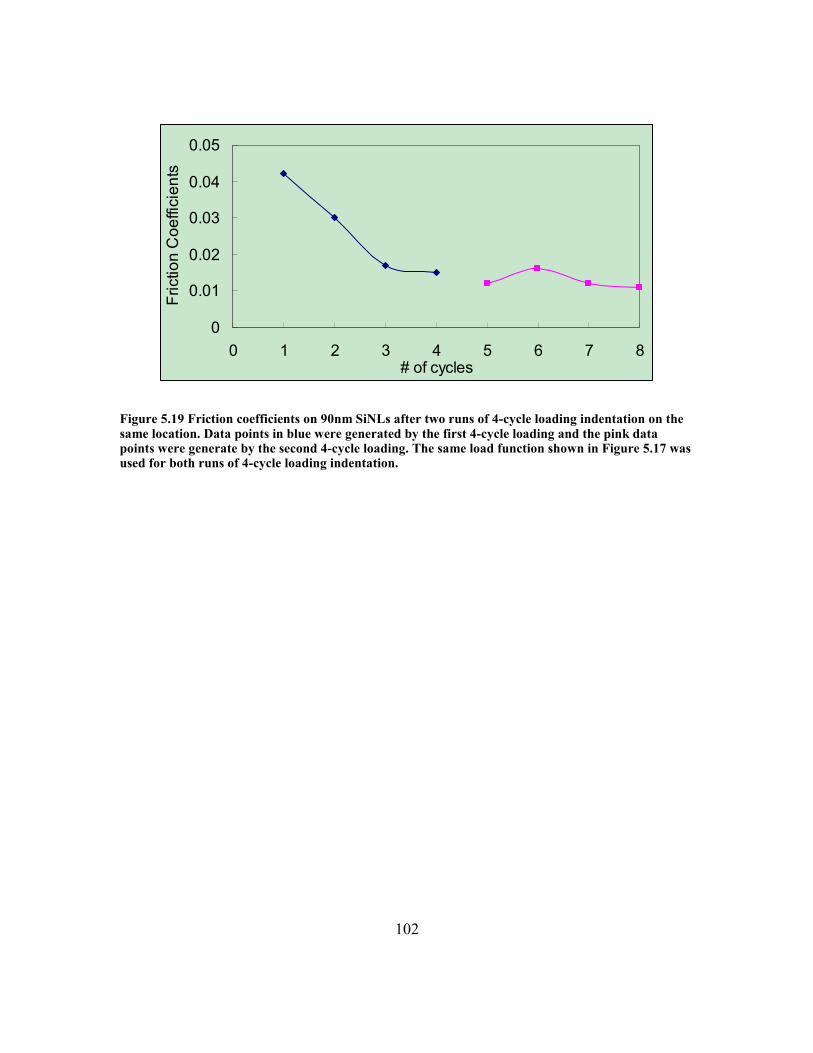
102
0
0.01
0.02
0.03
0.04
0.05
0 1 2 3 4 5 6 7 8# of cycles
Friction Coe
fficien
ts
Figure 5.19 Friction coefficients on 90nm SiNLs after two runs of 4-cycle loading indentation on the same location. Data points in blue were generated by the first 4-cycle loading and the pink data points were generate by the second 4-cycle loading. The same load function shown in Figure 5.17 was used for both runs of 4-cycle loading indentation.
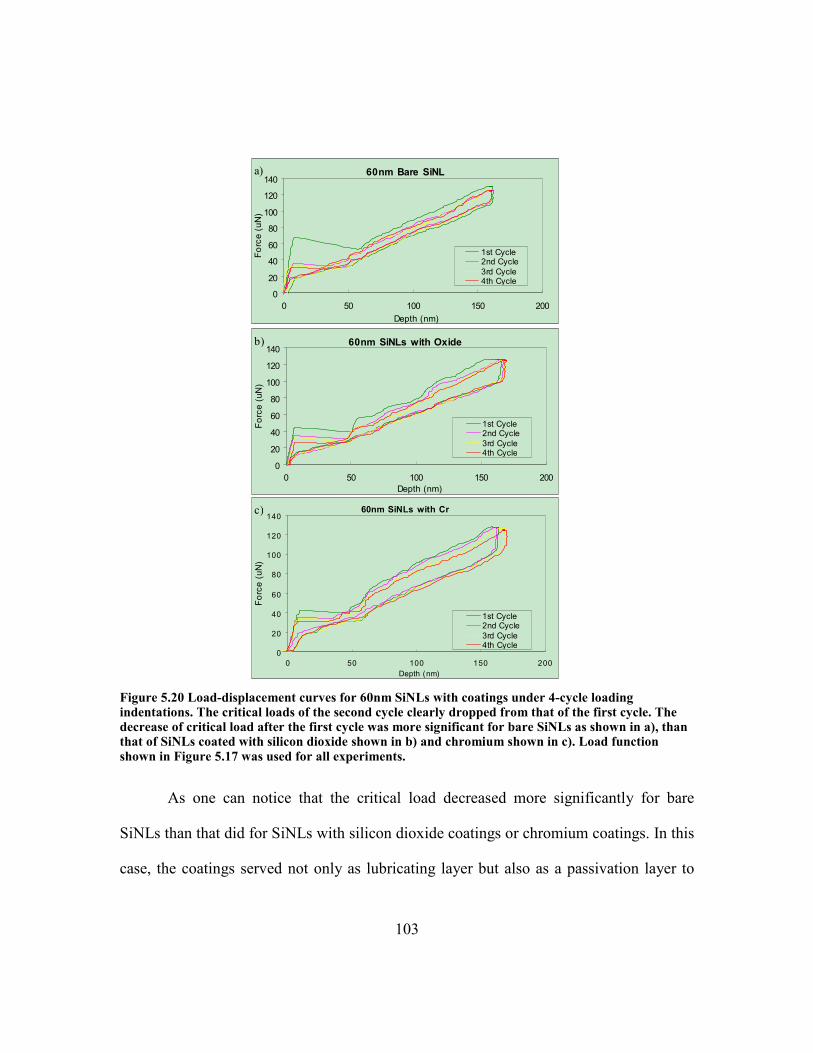
103
Figure 5.20 Load-displacement curves for 60nm SiNLs with coatings under 4-cycle loading indentations. The critical loads of the second cycle clearly dropped from that of the first cycle. The decrease of critical load after the first cycle was more significant for bare SiNLs as shown in a), than that of SiNLs coated with silicon dioxide shown in b) and chromium shown in c). Load function shown in Figure 5.17 was used for all experiments.
As one can notice that the critical load decreased more significantly for bare
SiNLs than that did for SiNLs with silicon dioxide coatings or chromium coatings. In this
case, the coatings served not only as lubricating layer but also as a passivation layer to
60nm Bare SiNL
0
20
40
60
80
100
120
140
0 50 100 150 200Depth (nm)
Force (uN)
1st Cycle2nd Cycle3rd Cycle4th Cycle
60nm SiNLs with Oxide
0
20
40
60
80
100
120
140
0 50 100 150 200Depth (nm)
Force (uN)
1st Cycle2nd Cycle3rd Cycle4th Cycle
60nm SiNLs with Cr
0
20
40
60
80
100
120
140
0 50 100 150 200Depth (nm)
Force (uN)
1st Cycle2nd Cycle3rd Cycle4th Cycle
a)
b)
c)
104
protect the silicon surface from morphology changes such as plasticity and phase
transitions.
Another interesting phenomenon is that the unloading curves match very nicely
for each loading cycle, which may indicate the cyclic loading has little effect on the
sliding friction. More understanding are needed for future study of the mechanics
responses and friction behaviors after the buckling occurrences.
Since no residual deformation left after indentation, it could be concluded that the
contact history did not cause significant geometry change of SiNLs. Therefore, based on
the same discussion in Section 5.4, the frictional shear stress should follow the same
trend as the friction coefficient. Thus the contact history should significantly decrease the
frictional shear stress of SiNLs, particularly after the first indentation cycle.
5.6 Summary
In Chapter 5, we investigated the effects due to the test environment and the
contact materials. The study on the environmental effect showed that humidity did not
have an apparent effect on the buckling behavior. The reason can be attributed to the high
contact pressure between the indenter and SiNLs surface, which squeezed out the water
layer. This led to the building up of an intimate contact where the reactive stress
overwhelmed the stress due to water adhesion.
This justified the selection of the Hertzian contact model over the DMT, JKR or
Maugis models to evaluate the contact area and the friction coefficient. On this basis, the
frictional shear stress was calculated for all test structures. The results showed that the
105
shear stress was independent on the line width of SiNLs and thus provided a better
description of the friction properties of the contact materials.
The critical buckling load was found to decrease when the surface was coated
with a silicon dioxide or chromium layer. This can be attributed to the change of contact
surfaces due to overlayer coatings. The coating may minimize the surface roughness and
the contact singularities of the SiNLs, resulting in a reduction of the critical load for
buckling. This was evidenced by the fact that the transfer of buckling mode II to mode I
was not observed for either set of test structures with oxide or chromium coating.
Under multi-cycle loading conditions, the critical buckling loads dropped
significantly after the first loading cycle. However, the mechanical strength of the SiNLs
test structures remained the consistent for each loading cycle. The contact history
therefore has significant impact on the contact surface but little impact on the SiNLs.
106
Chapter 6: Summary and Future Work
6.1 Summary
In this thesis work, we report a study of the mechanical behavior and contact
friction of silicon nanolines (SiNLs). The mechanical responses, especially the buckling
behavior and nanofriction of SiNLs, were studied by a nanoindentation technique. For
this study, we have developed a process based on e-beam lithography and anisotropic
etching which yielded SiNLs with line width as small as 25nm and with vertical sidewalls
almost atomically smooth. Using such structures, we have investigated the deformation
behavior of SiNLs and to measure the contact friction as a function of materials and
nanoline dimensions. The results of this study are presented in three chapters: in Chapter
3, the fabrication process of SiNLs; in Chapter 4, the buckling behavior of the silicon
nanolines and in Chapter 5, the nanofriction of the SiNLs.
The process developed to fabricate SiNLs test structures was described in Chapter 3.
This process was based on a combination of high resolution EBL and high quality pattern
transfer by AWE. The combination of these two techniques enabled us to obtain vertical
and smooth single-crystal SiNLs on (110) orientated Si. This fabrication process yielded
SiNLs with potential applications for nanograting-based sensors and interconnects. They
were well-suited for quantitative studies of mechanical and friction properties of silicon-
based structures at the nanoscale.
In Chapter 4, we report the results obtained from the study of the mechanical
behavior and friction properties of SiNLs using a nanoindentation technique. The SiNLs
107
test structures used in our experiments had height to width ratio from 10 to 20, making it
well suitable for the study of buckling behaviors. The loading-displacement indentation
curves showed that the critical load to induce the buckling of the SiNLs can be correlated
to the contact friction of the nano-indenter, the geometry of SiNLs, and the eccentricity of
the applied load. A map was built as a guideline to describe the buckling modes
observed. The map was divided into three regions where different regions correlate to
different buckling modes including Mode I, Mode II and sliding-bending of SiNLs. This
map agreed very well with the indentation results observed experimentally.
In Chapter 5, we investigated the effects due to the test environment and the
contact materials. The study on the environmental effect showed that the water
intermediate layer did not have an apparent effect on the buckling behavior. The reason
can be attributed to the high contact pressure between the indenter and SiNLs surface
which squeezed out the water layer. This led to the building up of an intimate contact
where the reactive stress overwhelmed the stress due to water adhesion. This verified the
use of a Hertzian contact model to evaluate the contact area and the friction coefficient.
On this basis, the frictional shear stress was calculated for all test structures. The results
showed that the shear stress was independent on the line width of SiNLs and thus
provided a better description of the friction properties of the contact materials.
The critical buckling load was found to decrease when the surface was coated
with a silicon dioxide or chromium layer. This can be attributed to the change of contact
surfaces due to the oxide or the chromium coating which apparently served as a lubricant
layer. The coating minimized the surface roughness and the contact singularities of the
SiNLs resulting in a reduction of the critical load for buckling. This was evidenced by the
108
fact that the transfer of buckling mode II to mode I was not observed for either set of test
structures with oxide or chromium coating.
Under multi-cycle loading conditions, the critical buckling loads dropped
significantly after the first loading cycle. However, the mechanical strength of the SiNLs
test structures remained the consistent for each loading cycle. The contact history
therefore has significant impact on the contact surface but little impact on the SiNLs.
6.2 Future Work
The average contact pressure on the SiNLs is on the order of 10GPa. Considering
the maximum contact pressure on asperities could be even higher than 10GPa, the local
contact pressure could be higher than 12GPa, which is around the contact pressure that
induces phase transformation of single-crystalline silicon. If phase transformation occurs
for the SiNLs in the nanoindentation experiments, the friction bonding nature could be
changed. Other probable changes of SiNLs under the nanoindentation include the
initiation of dislocations or micro-cracks. A closer look at the interfaces of contact and
perimeters are needed to understand the mechanisms of the effect of contact history on
friction. We have performed TEM imaging experiments on the sidewalls of SiNLs. From
the TEM images, a 10nm band was discovered which has apparently different contrast
compared to other regions of the images. There might have micro-structural changes or
dislocations in the regions which are 10nm away from the contact interface. More
systematic studies and TEM imaging could help to understand the mechanisms of contact
history.
The thickness of the coated silicon dioxide was 3nm, and the effect of surface
coating was significant on friction compared with bare SiNLs. Considering the thickness
109
of native oxide is around 1nm on the bare SiNLs, it is interesting to study the friction
behavior as a function of coating thickness. The results of this study could reveal the
effective friction bonding distance between silicon and diamond. The effect of contact
history could be very interesting if the thickness of the coating layer is around a critical
thickness.
The friction coefficients of 30nm SiNLs exhibited the largest variation. This
observation was similar to the 24nm SiNLs study by Bin Li. And we argued that Mode II
buckling actually did occur but we did not observe the second displacement burst on the
load-displacement curves, which means a transition of Mode II buckling to Mode I
buckling was not observed on the unloading process. The mechanism that determines the
transition of buckling mode is still not clear.
To derive an analytical solution of the buckling modes, 2D modes were employed
in current study. The confinement effect of SiNLs due the length and the spherical shape
of indenter were not studied. More accurate modes considering the 3D effect could help
to build a better map of buckling mode and solve the problem of transition of buckling
mode.
Diamond indenter was used in this study, and the SiNLs was coated with silicon
dioxide or chromium. Another way of changing the contact material is using another
indenter with different material, such as tungsten or silicon carbide.
Our nanoindenter system has the capabilities to perform nanoscratching test. The
nanoscratching test measures the lateral forces directly and it could provide a great
complimentary study to the nanoindentation. Actually, preliminary studies showed
consistent results with those two methods. To perform nanoscratching test, new test
structures with larger pitches and larger linewidth might be helpful at the starting point to
understand the mechanical behaviors of SiNLs. The lateral forces with current test

110
structures were in range of 0.5µN to 2µN. With larger linewidth, the lateral forces will
increase. With larger pitches, the interaction between SiNLs can be disentangled.
111
Selected Publications
1. Zhiquan Luo, Huai Huang, Ryan Scott Smith et. al., Nanoindentation study of friction and wear
of silicon nanolines, accepted by 2009 MRS Spring Meeting, San Francisco, April 16, 2009
2. Gopal A*, Luo Zhiquan*, Lee JY, Kumar K, Li B, Hoshino K, Schmidt C, Ho PS, Zhang X,
Nano-opto-mechanical characterization of neuron membrane mechanics under cellular growth
and differentiation, Biomedical Microdevices, 2008, 10(5): p.611-622. (*equal contributors)
3. Z. Luo, B. Li, P. S. Ho, R. Allen, M. W. Cresswell, J. Tom, M. Stevenson, B. Shulver, A. Walton,
Development of a Hybrid Lithography Process for Fabricating Test Structures Having Dense
Feature Linewidths Narrower Than 40nm, 51st International Conference on Electron, Ion, and
Photon Beam Technology & Nanofabrication, Denver, May 29-June 1, 2007
4. Zhiquan Luo, Bin Li, Paul S. Ho, Toh-Ming Lu, Nanoindentation Study of the Mechanical
Behavior of Silicon Nano-column Structures, Gordon Research Conference on Thin Film and
Small Scale Mechanical Behavior, Waterville, Maine, July 18-23, 2004.
5. Luo, Zhiquan; Luo, K.; Xie X.; Liu, Y.H.; Lu, L.; Xiao, L.; Ren, H.T.; Jiao, Y.L.; Zheng,
M.H.; Gao, Z.X. , Study on current-limiting mechanism in Bi1.8Pb0.34Sr2Ca2.2Cu3O8+x/Ag tapes bye
magneto-optic imaging, the International Conference on Engineering and Technology Sciences
▬ International Symposium on Advanced Materials, Beijing, China, Oct. 11, 2000.
6. Luo Zhiquan; Xie Xu; Luo Kang; Gao Zheng-Xiang; Duan Zhen-Zhong; Zhou Lian; Zhang
Ping-Xiang; Zheng Hui-Ling; Wu Xiao-Zu; Lin Wei; Deng Hua; Hua Pei-Wen, Web-like weak
superconducting regions in Bi-2223/Ag tape observed magneto-optic images, Chinese Journal of
Low Temperature Physics, 2000, 22(5), p. 349-352, 2000
7. Luo, Zhiquan; Liu, Y.H.; Lu, L.; Luo, K.; Xiao, L.; Ren, H.T.; Jiao, Y.L.; Zheng, M.H.; Gao,
Z.X., A new method to determine jc in bulk superconductor from saturated diamagnetic field by
magneto-optic imaging, Physica C, 2000, 341-348, p. 1465-1466
112
References
1. Patolsky, F., G. Zheng, and C.M. Lieber, Nanowire sensors for medicine and the life sciences.
Nanomedicine, 2006. 1(1): p. 51-65.
2. Xia, Y.N., et al., One-dimensional nanostructures: Synthesis, characterization, and
applications. Advanced Materials, 2003. 15(5): p. 353-389.
3. Knight, S., et al., Advanced metrology needs for nanoelectronics lithography. Comptes Rendus
Physique, 2006. 7(8): p. 931-941.
4. Yu, J.Y., S.W. Chung, and J.R. Heath, Silicon nanowires: Preparation, device fabrication, and
transport properties. Journal of Physical Chemistry B, 2000. 104(50): p. 11864-11870.
5. Wang, D.W., B.A. Sheriff, and J.R. Heath, Silicon p-FETs from ultrahigh density nanowire
arrays. Nano Letters, 2006. 6(6): p. 1096-1100.
6. Dixson, R.G., et al., Traceable calibration of critical-dimension atomic force microscope
linewidth measurements with nanometer uncertainty. Journal of Vacuum Science &
Technology B, 2005. 23(6): p. 3028-3032.
7. Lewcock, A. New nanotech anti-cancer drug delivery system introduced. 2007 [cited.
8. Dekker, C., Solid-state nanopores. Nat Nano, 2007. 2(4): p. 209-215.
9. Beal, J. New nanoparticle catalyst brings fuel-cell cars closer to showroom. 2008 [cited.
10. R. Arghavani, H.M.S., Despite engineering and cost challenges, 32nm node IC manufacturing
within reach. solid 2008. 51(5).
11. Appenzeller, J., What Promises do Nanotubes and Nanowires Hold for Future Nanoelectronics
Applications? 2008.
113
12. Hoffmann, S., et al., Measurement of the bending strength of vapor-liquid-solid grown silicon
nanowires. Nano Letters, 2006. 6(4): p. 622-625.
13. He, R.R. and P.D. Yang, Giant piezoresistance effect in silicon nanowires. Nature
Nanotechnology, 2006. 1(1): p. 42-46.
14. Kittl, J.A., et al., Phase effects and short gate length device implementation of Ni fully silicided
(FUSI) gates. Microelectronic Engineering, 2006. 83(11-12): p. 2117-2121.
15. Tabib-Azar, M., et al., Mechanical properties of self-welded silicon nanobridges. Applied
Physics Letters, 2005. 87(11).
16. Beckman, R.A., et al., Fabrication of conducting Si nanowire arrays. Journal of Applied
Physics, 2004. 96(10): p. 5921-5923.
17. Lieber, C.M., Nanoscale science and technology: Building a big future from small things. Mrs
Bulletin, 2003. 28(7): p. 486-491.
18. Mao, S.X., M.H. Zhao, and Z.L. Wang, Nanoscale mechanical behavior of individual
semiconducting nanobelts. Applied Physics Letters, 2003. 83(5): p. 993-995.
19. Zhang, X.J., et al., Micromachined silicon force sensor based on diffractive optical encoders
for characterization of microinjection. Sensors and Actuators a-Physical, 2004. 114(2-3): p.
197-203.
20. Li, X.D., et al., Nanoindentation of silver nanowires. Nano Letters, 2003. 3(11): p. 1495-1498.
21. Wu, Y.Y. and P.D. Yang, Direct observation of vapor-liquid-solid nanowire growth. Journal of
the American Chemical Society, 2001. 123(13): p. 3165-3166.
22. Islam, M.S., et al., A novel interconnection technique for manufacturing nanowire devices.
Applied Physics a-Materials Science & Processing, 2005. 80(6): p. 1133-1140.
114
23. Hu, J.T., T.W. Odom, and C.M. Lieber, Chemistry and physics in one dimension: Synthesis
and properties of nanowires and nanotubes. Accounts of Chemical Research, 1999. 32(5): p.
435-445.
24. Chung, S.W., J.Y. Yu, and J.R. Heath, Silicon nanowire devices. Applied Physics Letters,
2000. 76(15): p. 2068-2070.
25. Hudek, P., et al., Evaluation of chemically amplified deep UV resist for micromachining using
e-beam lithography and dry etching. Microelectronic Engineering, 1996. 30(1-4): p. 309-312.
26. Melosh, N.A., et al., Ultrahigh-density nanowire lattices and circuits. Science, 2003. 300(5616):
p. 112-115.
27. Zankovych, S., et al., Nanoimprint lithography: challenges and prospects. Nanotechnology,
2001. 12(2): p. 91-95.
28. Armacost, M., et al., Plasma-etching processes for ULSI semiconductor circuits. Ibm Journal
of Research and Development, 1999. 43(1-2): p. 39-72.
29. Cresswell, M.W., et al., Electrical linewidth test structures patterned in (100) silicon-on-
insulator for use as CD standards. Ieee Transactions on Semiconductor Manufacturing, 2001.
14(4): p. 356-364.
30. Chien, F.S.S., et al., Nanomachining of (110)-oriented silicon by scanning probe lithography
and anisotropic wet etching. Applied Physics Letters, 1999. 75(16): p. 2429-2431.
31. Cresswell, M.W., et al., RM 8111: Development of a prototype linewidth standard. Journal of
Research of the National Institute of Standards and Technology, 2006. 111(3): p. 187-203.
32. Petch, N.J., Citation classic - the cleavage strength of polycrystals. Current
Contents/Engineering Technology & Applied Sciences, 1982(19): p. 24-24.
115
33. Namazu, T., Y. Isono, and T. Tanaka, Evaluation of size effect on mechanical properties of
single crystal silicon by nanoscale bending test using AFM. Journal of
Microelectromechanical Systems, 2000. 9(4): p. 450-459.
34. Namazu, T., Y. Isono, and T. Tanaka, Plastic deformation of nanometric single crystal silicon
wire in AFM bending test at intermediate temperatures. Journal of Microelectromechanical
Systems, 2002. 11(2): p. 125-135.
35. Hsin, C.L., et al., Elastic Properties and Buckling of Silicon Nanowires. Advanced Materials,
2008. 20(20): p. 3919-+.
36. Oliver, W.C. and G.M. Pharr, An improved technique for determining hardness and elastic-
modulus using load and displacement sensing indentation experiments. Journal of Materials
Research, 1992. 7(6): p. 1564-1583.
37. Cook, R.F., Strength and sharp contact fracture of silicon. Journal of Materials Science, 2006.
41: p. 841-872.
38. Li, J., et al., Atomistic mechanisms governing elastic limit and incipient plasticity in crystals.
Nature, 2002. 418(6895): p. 307-310.
39. Chen, X., et al., On the uniqueness of measuring elastoplastic properties from indentation: The
indistinguishable mystical materials. Journal of the Mechanics and Physics of Solids, 2007.
55(8): p. 1618-1660.
40. Hung, S.C., et al., Shell buckling behavior investigation of individual gallium nitride hollow
nanocolumn. Applied Physics a-Materials Science & Processing, 2006. 84(4): p. 439-443.
41. Li, M., H.X. Tang, and M.L. Roukes, Ultra-sensitive NEMS-based cantilevers for sensing,
scanned probe and very high-frequency applications. Nature Nanotechnology, 2007. 2(2): p.
114-120.
42. Bec, S., A. Tonck, and J. Fontaine. Nanoindentation and nanofriction on DLC films. 2006:
Taylor & Francis Ltd.
116
43. D. Dowson, History of Tribology. 1979, Longman: London.
44. F.P. Bowden, D.T., The friction and lubrication of solids 1950: Oxford : Clarendon Press.
45. Autumn, K., et al., Frictional adhesion: a new angle on gecko attachment. Journal of
Experimental Biology, 2006. 209(18): p. 3569-3579.
46. Masuda, H. and F. Honda, Low friction of a diamond/H-terminated, Si(111) sliding system.
Ieee Transactions on Magnetics, 2003. 39(2): p. 903-908.
47. Borodich, F.M. and L.M. Keer, Contact problems and depth-sensing nanoindentation for
frictionless and frictional boundary conditions. International Journal of Solids and
Structures, 2004. 41(9-10): p. 2479-2499.
48. Guruzu, S., et al., Friction-induced formation of nanocrystals on Si. Wear, 2005. 259(1-6): p.
524-528.
49. Ivashchenko, V.I., et al., Tribology of amorphous, nanocrystalline, and crystalline slabs of Si,
C, and SiC. Physical Review B, 2005. 72(11).
50. Zhupanska, O.I. and A.F. Ulitko, Contact with friction of a rigid cylinder with an elastic half-
space. Journal of the Mechanics and Physics of Solids, 2005. 53(5): p. 975-999.
51. Rubinstein, S.M., G. Cohen, and J. Fineberg, Contact area measurements reveal loading-
history dependence of static friction. Physical Review Letters, 2006. 96(25).
52. Gao, G.T., et al., Atomic-scale friction on diamond: A comparison of different sliding
directions on (001) and (111) surfaces using MD and AFM. Langmuir, 2007. 23(10): p. 5394-
5405.
53. Xu, D.W., Scale dependence in friction: the transition from intimate contact to monolayer
lubricated contact. 2007, the University of Texas at Austin: Austin.
54. Dintwa, E., E. Tijskens, and H. Ramon, On the accuracy of the Hertz model to describe the
normal contact of soft elastic spheres. Granular Matter, 2008. 10(3): p. 209-221.
117
55. Li, Q.Y. and K.S. Kim, Micromechanics of friction: effects of nanometre-scale roughness.
Proceedings of the Royal Society a-Mathematical Physical and Engineering Sciences, 2008.
464(2093): p. 1319-1343.
56. Szlufarska, I., M. Chandross, and R.W. Carpick, Recent advances in single-asperity
nanotribology. Journal of Physics D-Applied Physics, 2008. 41(12).
57. Xu, D.W., K. Ravi-Chandar, and K.A. Liechti, On scale dependence in friction: Transition
from intimate to monolayer-lubricated contact. Journal of Colloid and Interface Science, 2008.
318(2): p. 507-519.
58. Yang, Z.P., H.P. Zhang, and M. Marder, Dynamics of static friction between steel and silicon.
Proceedings of the National Academy of Sciences of the United States of America, 2008.
105(36): p. 13264-13268.
59. He, G., M.H. Muser, and M.O. Robbins, Adsorbed layers and the origin of static friction.
Science, 1999. 284(5420): p. 1650-1652.
60. He, G. and M.O. Robbins, Simulations of the static friction due to adsorbed molecules.
Physical Review B, 2001. 64(3).
61. Homola, A.M., et al., Measurements of and relation between the adhesion and friction of 2
surfaces separated by molecularly thin liquid-films. Journal of Tribology-Transactions of the
Asme, 1989. 111(4): p. 675-682.
62. Homola, A.M., et al., Fundamental experimental studies in tribology- the transition from
interfacial friction of undamaged molecularly smooth surfaces to normal friction with wear..
Wear, 1990. 136(1): p. 65-83.
63. Enachescu, M., et al., UHV AFM study of an ideally hard contact: The diamond(111)-WC
interface. Abstracts of Papers of the American Chemical Society, 1999. 217: p. U625-U625.
64. Enachescu, M., et al., Observation of proportionality between friction and contact area at the
nanometer scale. Tribology Letters, 1999. 7(2-3): p. 73-78.
118
65. P.Timoshenko, S. and J.M. Gere, Theory of Elastic Stability. Second Edition ed. 1961,
Singapore: McGraw-Hill Book Company.
66. Hertz, H., On the contact of elastic solids. J. Reine Angewandte Math., 1882. 94: p. 6.
67. Derjaguin, B.V., V.M. Muller, and Y.P. Toporov, Effect of contact deformations on adhesion
of particles. Journal of Colloid and Interface Science, 1975. 53(2): p. 314-326.
68. Johnson, K.L., K. Kendall, and A.D. Roberts, Surface Energy and the Contact of Elastic
Solids. Proceedings of the Royal Society of London. Series A, Mathematical and Physical
Sciences (1934-1990), 1971. 324(1558): p. 301-313.
69. Maugis, D., Adhesion of spheres- the JKR-DMT transition using a Dugdale model. Journal of
Colloid and Interface Science, 1992. 150(1): p. 243-269.
70. Barthel, E., Adhesive elastic contacts: JKR and more. Journal of Physics D-Applied Physics,
2008. 41(16).
71. Eichenlaub, S., G. Kumar, and S. Beaudoin, A modeling approach to describe the adhesion of
rough, asymmetric particles to surfaces. Journal of Colloid and Interface Science, 2006.
299(2): p. 656-664.
72. Johnson, K.L. and J.A. Greenwood, An adhesion map for the contact of elastic spheres.
Journal of Colloid and Interface Science, 1997. 192(2): p. 326-333.
73. Ranade, M.B., Adhesion and removal of fine particles on surfaces.. Aerosol Science and
Technology, 1987. 7(2): p. 161-176.
74. Tabor, D., Surface forces and surface interactions. Journal of Colloid And Interface Science
1977. 58(1): p. 12.
75. Irving, S. and P.J. M., Chapter 17, in Introduction to Solid Mechanics. 1996, Prentice Hall;.
76. Vieu, C., et al., Electron beam lithography: resolution limits and applications. Applied Surface
Science, 2000. 164: p. 111-117.
119
77. Gary S. May, C.J.S., Introduction to Semiconductor Manufacturing, in Fundamentals of
Semiconductor Manufacturing and Process Control. 2006. p. 1-24.
78. Zhang, Y.Y., et al., Fabrication of silicon-based multilevel nanostructures via scanning probe
oxidation and anisotropic wet etching. Nanotechnology, 2005. 16(4): p. 422-428.
79. Li, B., et al., Fabrication and characterization of patterned single-crystal silicon nanolines.
Nano Letters, 2008. 8(1): p. 92-98.
80. Li, B., Fabrication of silicon-based nano-structures and the effects of scaling on their
mechanical and electrical properties. 2007, the University of Texas at Austin.
81. Inc.Hysitron, TriboScope Users Manual: Minneapollis.
120
Vita
Zhiquan Luo was born in Sichuan, China, on March 2, 1976. He received the B.S.
(1999) and M.S. (2001) in Physics from Beijing University, Beijing, China. From 1999,
he worked as a graduate research assistant in the Physics Department of Beijing
University until 2001. Since 2001, he has been pursuing his Ph.D. degree in Physics
Department at the University of Texas at Austin. His current research interest is in the
area of fabrication and characterization of nano-scale structures, and their applications in
pharmaceutical and microelectronic industry.
Permanent address: SiXian 5-2, Anyue, Sichuan Province 642350, the People’s
Republic of China.
This dissertation was typed by Zhiquan Luo.


![YADONG LUO - University of Miami School of Business ...11] Shenkar, Oded and Yadong Luo. 2003. International Business, John Wiley & Sons, 1st Edition. [10] Luo, Yadong (2002). Multinational](https://img.pdfslide.us/doc/110x75/5aa1240f7f8b9a8e178ef5ee/yadong-luo-university-of-miami-school-of-business-11-shenkar-oded-and-yadong.jpg)