Embed Size (px)
Citation preview
Copyright
by
Troy Christopher Messina
2002
The Dissertation Committee for Troy Christopher Messinacertifies that this is the approved version of the following dissertation:
Steric Effects in the Metallic-Mirror to
Transparent-Insulator Transition in YHx
Committee:
John T. Markert, Supervisor
Alex de Lozanne
Ken Shih
Jack Swift
David Vanden Bout
Steric Effects in the Metallic-Mirror to
Transparent-Insulator Transition in YHx
by
Troy Christopher Messina, B.S., M.A.
DISSERTATION
Presented to the Faculty of the Graduate School of
The University of Texas at Austin
in Partial Fulfillment
of the Requirements
for the Degree of
DOCTOR OF PHILOSOPHY
THE UNIVERSITY OF TEXAS AT AUSTIN
December 2002

dedicated to Mom, Dad, Todd, and Jodi, the wizards behind the curtain
Acknowledgments
I would like to thank Dr. John Markert, an amazing scientist, an outstanding
advisor and teacher, and a wonderful friend. I only wish I had known I could call
him “John” sooner. I also must thank my coworkers because, at least most of them,
made life in the lab enjoyable. I thank Michelle Chabot for the random way she ran
her day-to-day life and her assistance with late night, last minute data collecting.
Gergana Drandova gave me many inspiring conversations about culture, computers,
and Metallica. Yong Lee seems to know something about everything which I have
a question. Lizz Judge, if nothing else, knew EVERY completely obscure crossword
answer. Casey Miller reminded me (twice) not to date physics students; fortunately,
for Casey, the third time is the charm. Congratulations, stud!!! Also, without Casey,
many of the results of this dissertation would not exist! Sean Rabun faithfully
tested unused equipment to see what worked and what didn’t. Natalie Sidarous was
always diligent in the lab even when everyone else chose to be social. Thanks to
everyone in the de Lozanne and Erskine labs who gave me advice when I was lost. A
special recognition goes to Alan Schroeder, Jesse Martinez, Harold Williams, John
England, and all of the others on the 3rd floor of RLM that make things work. The
University of Texas is so incredibly fortunate to have such a competent team. The
last physics acknowledgement goes to Ronald Griessen and his team of researchers
in Amsterdam, Holland for discovering the topic of my dissertation and assisting
me during my tenure at UT. Their expert knowledge often shed light on very dark
v
situations.
Outside of physics... My closest friend and wife, Jodi, thank you for believing
in me, having patience, and offering to spend the rest of your life with me. I have
to “shout out” to the five greatest friends in the world, Tommy, Brian (B.J.), Bryan
(NYC), Skaughtt, and dAVE. I wouldn’t have made it here without you guys. Next,
thanks to my brother, Todd, a.k.a. Julian, who kept me clothed in hand-me-downs
and protected me from bullies all my life. Next to last, thanks go to all of my
musical compadres in Megalo, Chester, and 3 Penny Opera who have helped me
continue my other passion.
This last acknowledgement deserves his own paragraph. One might find this
humorous since my wife, family, and friends were lumped into a single paragraph.
However, if it weren’t for Jack Clifford I would never have been able to build the
experiments that brought me to the point of writing this dissertation. Jack’s assis-
tance went far beyond a consultant in the machine shop. Jack is an incredible friend
who I will miss dearly when I leave UT.
. . .
vi
Steric Effects in the Metallic-Mirror to
Transparent-Insulator Transition in YHx
Publication No.
Troy Christopher Messina, Ph.D.
The University of Texas at Austin, 2002
Supervisor: John T. Markert
We have exploited the switchable mirror transition, from metallic mirror to transpar-
ent insulator, in YHx to study steric effects due to scandium (Sc) substitution into
the Y lattice. The reduction of lattice dimension upon Y replacement with Sc lends
insight into the dynamics of this dramatic phase transition. Electron-beam evapora-
tion was used to deposit 100 nm thick films of Y1−xScx alloys for 0.00 ≤ x ≤ 1.00.
The films are capped with a protective, 10 nm overlayer of palladium (Pd) to pre-
vent oxidation and to catalyze hydrogen absorption. Despite a significant decrease
in the unit cell volume of approximately 30%, optical spectral transmission and
resistivity measurements reveal that a transition persists far into the alloy phase
diagram. The optical transmittance behavior smoothly transitions from trihydride
behavior to dihydride behavior with a total decrease in optical transmittance by
a factor of 12. Electrical resistivity measurements indicate a similar reduction in
the metal to insulator transition with Sc concentration. In addition, large disorder
vii

of ρdo ≈ 120 µΩ·cm is introduced due to alloying. Details of stuctural analysis,
spectroscopy, and electrical transport are discussed.
viii
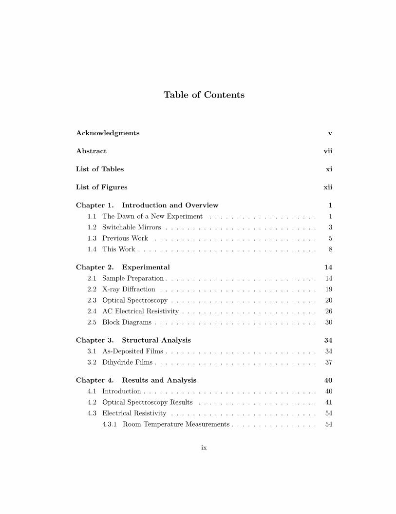
Table of Contents
Acknowledgments v
Abstract vii
List of Tables xi
List of Figures xii
Chapter 1. Introduction and Overview 1
1.1 The Dawn of a New Experiment . . . . . . . . . . . . . . . . . . . . 1
1.2 Switchable Mirrors . . . . . . . . . . . . . . . . . . . . . . . . . . . . 3
1.3 Previous Work . . . . . . . . . . . . . . . . . . . . . . . . . . . . . . 5
1.4 This Work . . . . . . . . . . . . . . . . . . . . . . . . . . . . . . . . . 8
Chapter 2. Experimental 14
2.1 Sample Preparation . . . . . . . . . . . . . . . . . . . . . . . . . . . . 14
2.2 X-ray Diffraction . . . . . . . . . . . . . . . . . . . . . . . . . . . . . 19
2.3 Optical Spectroscopy . . . . . . . . . . . . . . . . . . . . . . . . . . . 20
2.4 AC Electrical Resistivity . . . . . . . . . . . . . . . . . . . . . . . . . 26
2.5 Block Diagrams . . . . . . . . . . . . . . . . . . . . . . . . . . . . . . 30
Chapter 3. Structural Analysis 34
3.1 As-Deposited Films . . . . . . . . . . . . . . . . . . . . . . . . . . . . 34
3.2 Dihydride Films . . . . . . . . . . . . . . . . . . . . . . . . . . . . . . 37
Chapter 4. Results and Analysis 40
4.1 Introduction . . . . . . . . . . . . . . . . . . . . . . . . . . . . . . . . 40
4.2 Optical Spectroscopy Results . . . . . . . . . . . . . . . . . . . . . . 41
4.3 Electrical Resistivity . . . . . . . . . . . . . . . . . . . . . . . . . . . 54
4.3.1 Room Temperature Measurements . . . . . . . . . . . . . . . . 54
ix
4.3.2 Temperature-Dependent Measurements . . . . . . . . . . . . . 60
4.4 Discussion . . . . . . . . . . . . . . . . . . . . . . . . . . . . . . . . . 68
Chapter 5. Summary and Future Investigations 75
Appendices 77
Appendix A. Vacuum and Film Deposition 78
A.1 Growing a Film . . . . . . . . . . . . . . . . . . . . . . . . . . . . . . 78
A.2 Some Suggested Modifications . . . . . . . . . . . . . . . . . . . . . . 80
Appendix B. LabVIEW VIs 81
B.1 Room Temperature VI . . . . . . . . . . . . . . . . . . . . . . . . . . 81
B.2 Temperature Dependent VI . . . . . . . . . . . . . . . . . . . . . . . 84
Appendix C. Nuclear Magnetic Resonance Force Microscopy 92
C.1 NMR–FM Overview . . . . . . . . . . . . . . . . . . . . . . . . . . . 92
C.2 Oscillators . . . . . . . . . . . . . . . . . . . . . . . . . . . . . . . . . 99
C.3 Micro–Magnets . . . . . . . . . . . . . . . . . . . . . . . . . . . . . . 100
C.4 Magnet-on-Oscillator Characterization . . . . . . . . . . . . . . . . . 103
Appendix D. Some Pictures 107
Bibliography 113
Vita 126
x
List of Tables
4.1 Fit parameters from the Lambert-Beer model of the transmission edge forY1−zSczH3−δ. . . . . . . . . . . . . . . . . . . . . . . . . . . . . . . . 55
C.1 Quality factors, spring constants, and minimal detectable forces for oscilla-tors prior to magnet deposition. . . . . . . . . . . . . . . . . . . . . . . 99
C.2 Comparison of calculated and measured forces from micro–magnets on can-tilevers. . . . . . . . . . . . . . . . . . . . . . . . . . . . . . . . . . . . 105
xi
List of Figures
1.1 An optically switching yttrium film. Before hydrogen is introduced, thefilm reflects the American flag. After hydrogen has time to infuse, thefilm becoms visibly more transparent, and one can see objects behind thesubstrate (the longhorn). . . . . . . . . . . . . . . . . . . . . . . . . . . 2
1.2 Dissociation of H2 at the surface of a metal film capped with Pd. . . . . . 4
1.3 Hydrogen loading phenomena for a 100 nm Y film capped with 10 nm ofPd. On the left axis is the normalized transmittance at 700 nm. On theright axis is the resistivity. The scale at the bottom gives approximately theYHx phases corresponding to the graphical data. The arbitrary timescaleis roughly in seconds. . . . . . . . . . . . . . . . . . . . . . . . . . . . . 5
1.4 Hydride structure and phase diagram for Y. There are three distinct phases:α (hcp monohydride), β (fcc dihydride), and γ (hcp trihydride). . . . . . . 7
1.5 Hexagonal lattice with corresponding tetrahedral (a) and octahedral (b) sites. 9
1.6 Face-centered cubic lattice with corresponding tetrahedral (a) and octahe-dral (b) sites. . . . . . . . . . . . . . . . . . . . . . . . . . . . . . . . . 10
1.7 Hydride structure and phase diagram for Sc. There are two distinct phases:α (fcc monohydride) and β (fcc dihydride). . . . . . . . . . . . . . . . . 12
1.8 Phase diagram for the Y1−zScz alloy system. The diagram indicates a solidsolution is possible of all alloys of Y-Sc. . . . . . . . . . . . . . . . . . . 13
2.1 Vacuum chamber used for metal-hydride film growth: 1a-b) Leybold crystalgrowth monitors, 2) rotating substrate/shutter feedthrough, 3-4) e-beamevaporators, 5) leak valve, 6) e-beam evaporator power supply, 7) turboand roughing pump station, 8) substrate viewport. . . . . . . . . . . . . 16
2.2 Pendant-drop electron beam evaporator. The rectangular section on the leftimage is blown up in the image on the right. 1) Sample rod, 2) filament, 3)linear-motion sample manipulator, 4) external electrical connections. . . . 17
2.3 Diagram for Bragg scattering and diffraction of x-rays from parallel layers ofa material. The bolded lines identify the path difference of the two outgoingrays. . . . . . . . . . . . . . . . . . . . . . . . . . . . . . . . . . . . . 19
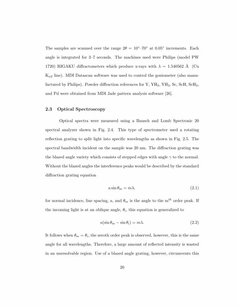
2.4 Bausch and Lomb Optical Spectrometer: (1) customized sample insert tube,(2) wavelength selector (340–960 nm), (3) switch box for in-line and van derPauw resistivity, (4) film mounting apparatus for 4-point resistivity andsimultaneous optical transmission measurements during hydrogen loading. 21
xii
2.5 Schematic of the Bausch & Lomb Spectronic 20 rotating reflection grating. 222.6 White light incident on the blaze angle reflection grating is split into con-
stituent colors, which one can select on the spectrometer based on the angleof the reflection grating. . . . . . . . . . . . . . . . . . . . . . . . . . . 23
2.7 Current-to-voltage circuit diagram for the photodiode measuring opticaltransmission in the Bausch and Lomb spectrometer. The graph shows atypical photodiode response as a function of incident wavelength. The solidline is the baseline due to dark current. . . . . . . . . . . . . . . . . . . 25
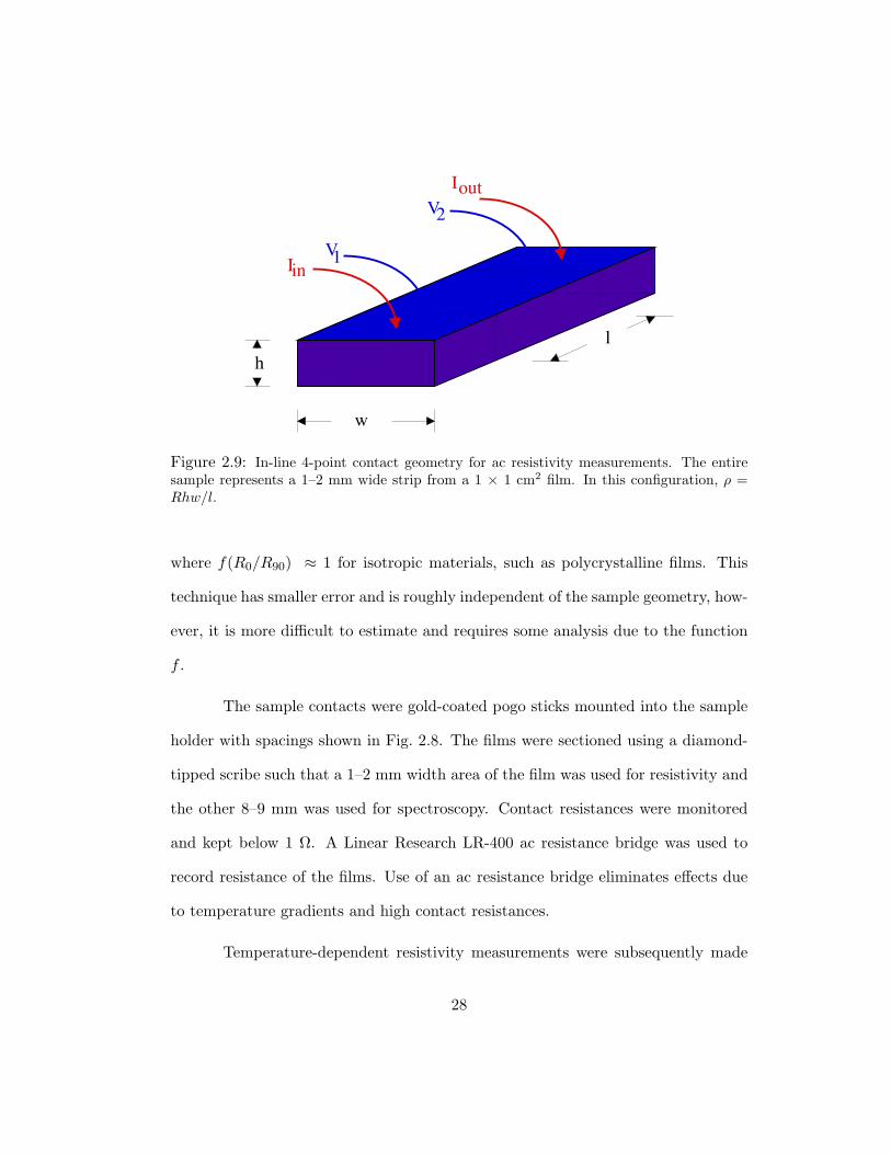
2.8 Contact configuration of the room temperature resistivity probe. . . . . . 272.9 In-line 4-point contact geometry for ac resistivity measurements. The entire
sample represents a 1–2 mm wide strip from a 1 × 1 cm2 film. In thisconfiguration, ρ = Rhw/l. . . . . . . . . . . . . . . . . . . . . . . . . . 28
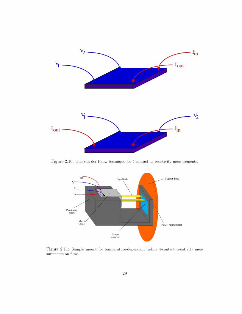
2.10 The van der Pauw technique for 4-contact ac resistivity measurements. . . 292.11 Sample mount for temperature-dependent in-line 4-contact resistivity mea-
surements on films. . . . . . . . . . . . . . . . . . . . . . . . . . . . . . 292.12 Block diagram of the room temperature optical spectroscopy and resistivity
measurement system. Transmission spectroscopy (340–960 nm wavelengths)was measured simultaneously with electrical resistivity. Phototransmissioninduces a current in a photodiode, which was converted to voltage andmeasured with a Keithley 195 DMM. In-line 4-point resistivity was measuredwith an LR-400 ac resistance bridge. All measurements were recorded usingLabview v.6. . . . . . . . . . . . . . . . . . . . . . . . . . . . . . . . . 31
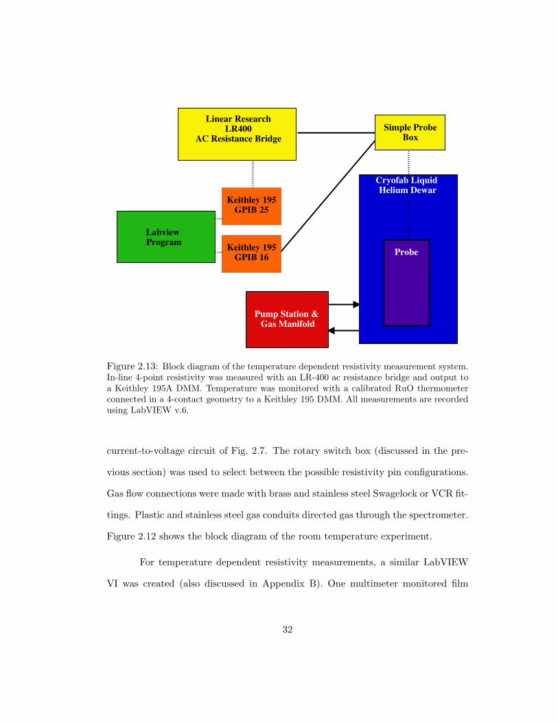
2.13 Block diagram of the temperature dependent resistivity measurement sys-tem. In-line 4-point resistivity was measured with an LR-400 ac resistancebridge and output to a Keithley 195A DMM. Temperature was monitoredwith a calibrated RuO thermometer connected in a 4-contact geometry toa Keithley 195 DMM. All measurements are recorded using LabVIEW v.6. 32
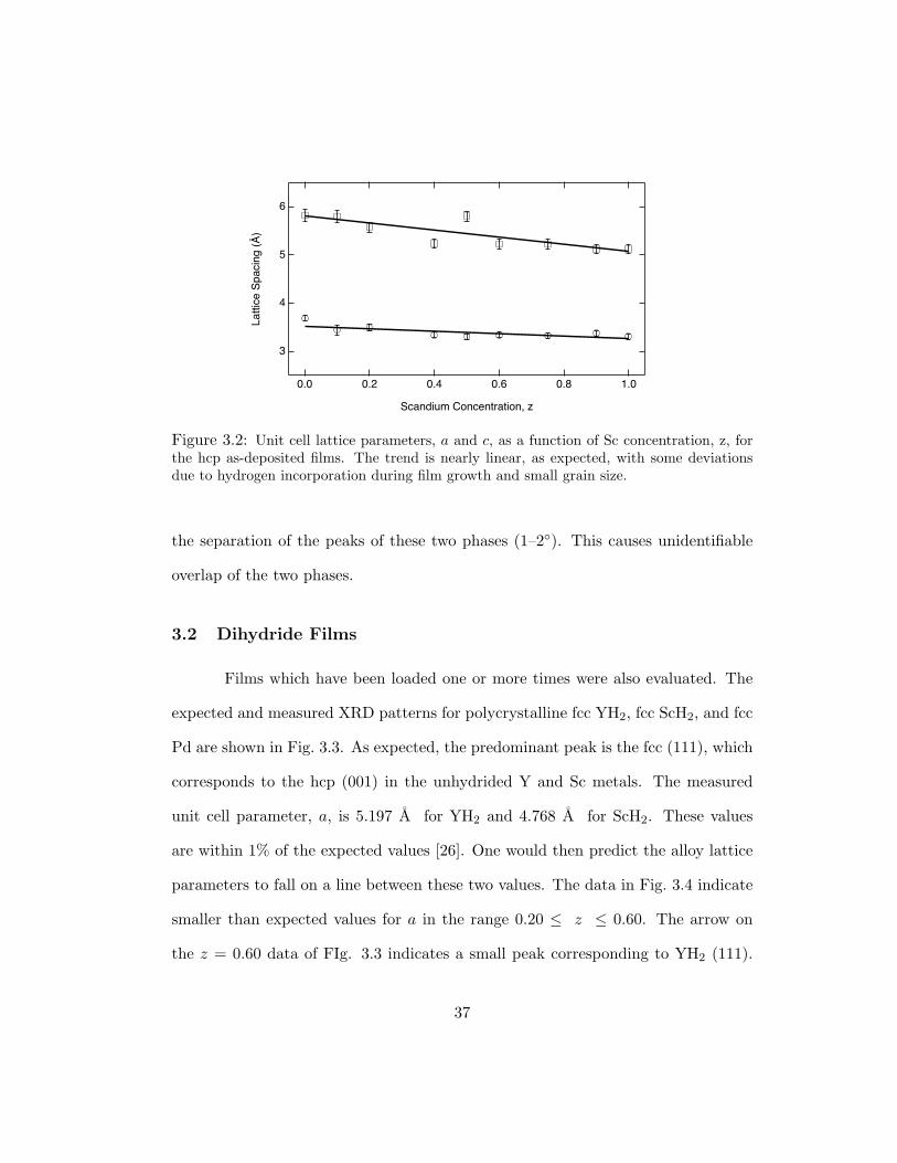
3.1 Expected and measured x-ray diffraction patterns for the as-deposited films. 353.2 Unit cell lattice parameters, a and c, as a function of Sc concentration, z,
for the hcp as-deposited films. The trend is nearly linear, as expected, withsome deviations due to hydrogen incorporation during film growth and smallgrain size. . . . . . . . . . . . . . . . . . . . . . . . . . . . . . . . . . 37
3.3 Expected and measured x-ray diffraction patterns for the dihydride concen-tration films. . . . . . . . . . . . . . . . . . . . . . . . . . . . . . . . . 38
3.4 Unit cell lattice parameter, a, as a function of Sc concentration, z, for thefcc dihydride films. . . . . . . . . . . . . . . . . . . . . . . . . . . . . . 39
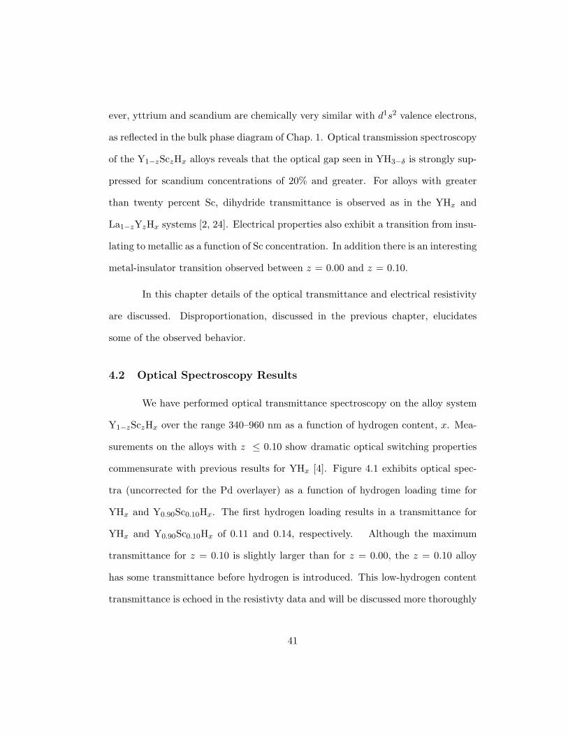
4.1 Optical transmittance spectra as a function of hydrogen loading time (inarbitrary units) starting from as-deposited films of Y and Y0.90Sc0.10. Theoptical switching capability is approximately equivalent for both samples.The full loading time scale is typically 1–2 hours. . . . . . . . . . . . . . 42
xiii
4.2 Optical transmittance spectra as a function of hydrogen loading time (inarbitrary units) starting from as-deposited films Y0.80Sc0.20 and Sc. Thevertical axis is scaled to that of the z = 0.00 and z = 0.10 samples. Theloss of optical switching capability is evident. The full loading time scale istypically 1–2 hours. . . . . . . . . . . . . . . . . . . . . . . . . . . . . . 43
4.3 Optical transmittance as a function of hydrogen loading time (in arbitraryunits) starting from unloaded (x ≈ 2) films of YHx and Y0.90Sc0.10Hx. Thefull loading time scale is typically 1–2 hours. . . . . . . . . . . . . . . . . 45
4.4 Optical transmittance spectra as a function of hydrogen loading time (inarbitrary units) starting from unloaded films (near x = 2) of Y0.80Sc0.20Hx
and ScHx. The full loading time scale is typically 1–2 hours. . . . . . . . . 46
4.5 Optical transmittance spectra as a function of hydrogen loading time (inarbitrary units) starting from an as-deposited film of Y0.60Sc0.40. This alloyexhibits phase separation upon hydrogenation. The spectrum, therefore,has a trihydride-like appearance with maximal transmittance at λ = 960nm due to YH3 formation. The full loading time scale is typically 1–2 hours. 47
4.6 Optical transmittance spectra as a function of hydrogen loading time (inarbitrary units) starting from as-deposited (top) and unloaded (bottom)films of Y0.50Sc0.50Hx. The unloaded film is expected to have x ≈ 2. Thefull loading time scale is typically 1–2 hours. . . . . . . . . . . . . . . . . 48
4.7 Transmittance and ac resistivity as a function of hydrogen loading time. Theloading time is arbitrary and has not been scaled in any way. The hydrogenloading time ranged from 10 minutes to 2 hours. The transmittance isplotted for the wavelength of maximum dihydride transmittance. Dihydridetransmittance appears as a small peak or a shoulder on the transmittancecurve and is indicated by the vertical arrows. . . . . . . . . . . . . . . . 50
4.8 Transmittance at λ = 820 nm (ω = 1.51 eV) as a function of Sc concen-tration z. The amount of transmittance for fully loaded films approachesthat of unloaded films (near x = 2) with increasing z indicating a loss ofoctahedral site occupancy for trihydride formation. The lines are shown toguide the eye. The scatter in the data may be due to atomic disorder effectsor phase separation. . . . . . . . . . . . . . . . . . . . . . . . . . . . . 51
4.9 (a) Fully hydrogen loaded and (b) unloaded (near x = 2) film optical spectrashowing transmittance maxima dependence on alloy composition. . . . . . 52
4.10 Energy of maximum transmittance (for the range 1.29 ≤ ω ≤ 3.65 eV) as afunction of Sc concentration, z. The transparency energy of the fully loadedfilms approaches that of the unloaded films (near x = 2) as z increases. Thelines are shown to guide the eye. The scatter in the data may be due toatomic disorder effects. . . . . . . . . . . . . . . . . . . . . . . . . . . . 53
4.11 Lambert-Beer fits to the transmission edge. . . . . . . . . . . . . . . . . 55
xiv
4.12 Room temperature resistivity of several alloys as a function of hydrogenloading time in arbitrary units. The data has been scaled so that the di-hydride minimum is at the same time. The transition from the dihydrideminimum to trihydride maximum reduces with concentration until, in scan-dium the resistivity stays in the dihydride minimum. . . . . . . . . . . . 57
4.13 Modeling of disorder in room temperature electrical resistivity from Eqn. 4.1. 59
4.14 Temperature dependence of the ac resistivity for dihydrides of several alloys.All show metallic behavior with the exception of Y0.90Sc0.10. . . . . . . . 61
4.15 Temperature dependence of the ac resistivity for fully hydrogenated (295 K;1 atm H2) films of the same alloys as Fig. 4.14. YH3−δ and Y0.90Sc0.10H3−δ
indicate insulating behavior at low temperatures with an up-turned resis-tivity. A transition occurs from z = 0.10 and z = 0.20 supporting thespectroscopy results. . . . . . . . . . . . . . . . . . . . . . . . . . . . . 62
4.16 Temperature dependence of the resistivity over the range 4–150 K. The topgraph shows that, for 50–150 K, YH3−δ is most linear when plotted as ρ vs.ln (T ), while in the bottom plot, Y0.90Sc0.10H3−δ and Y0.80Sc0.20H2+δ showlinear behavior only at lower temperatures (4–20 K) when plotted as ln(ρ)vs. T−1/4, indicating a variable range hopping model. . . . . . . . . . . . 63
4.17 Temperature dependence of alloys with z > 0.20. Qualitatively the data issimilar for all alloys with z ≥ 0.20. The low temperature up-turn is bestmodeled with a Mott transition (T−1/4). . . . . . . . . . . . . . . . . . . 65
4.18 Scandium resistivity for 4–50 K. The data is plotted as ρ ∝ ln(T ) on topand ln(ρ) ∝ T−1/4) on bottom. The best agreement is with the Mott model. 66
4.19 Films of YH3−δ showing a temperature induced shunt and a hydrogen con-tent induced shunt. These resistivities are calculated assuming a film thick-ness of 110 nm. The resistivity near 4 K is equivalent to that of palladiumwhen calculated for a 10 nm film. . . . . . . . . . . . . . . . . . . . . . 67
4.20 A plot of the fraction of octahedral sites that have n scandium nearestneighbors as a function of scandium concentration. The dashed lines indi-cate the region where the metallic-mirror to transparent-insulator transitionis largely quenched. . . . . . . . . . . . . . . . . . . . . . . . . . . . . . 69
4.21 Expected maximum hydrogen content as calculated from data observationsand the combinatorics of Fig. 4.20. . . . . . . . . . . . . . . . . . . . . . 71
4.22 Revisiting the data of Fig. 4.8, the fully loaded transmittance as a functionof scandium content has been fit in proportion to the hydrogen contentpredicted by restricting octahedral occupancy to sites with n = 0 or n = 0and 1 nearest-neighbor scandiums. . . . . . . . . . . . . . . . . . . . . . 72
4.23 Phase diagrams for the 3-element system with the maximal hydrogen con-tents calculated from the model discussed in the text. a) assumes n = 0and b) n = 0 and 1. . . . . . . . . . . . . . . . . . . . . . . . . . . . . 73
xv
B.1 Room temperature spectrometry and resistivity LabVIEW VI front panel. 82
B.2 The opening sequence of the room temperature VI. This sequence sets up thetimer and opens a file with column headers for writing data. The time andfile information are sent into a while loop that runs until the stop button isclicked. The while loop contains sequential frames which do all of the otheroperations. . . . . . . . . . . . . . . . . . . . . . . . . . . . . . . . . . 83
B.3 The second frame of the room temperature VI. The values for resistanceand transmittance voltages are formatted and converted to strings. . . . . 85
B.4 Final frame of the VI. The characters for the time, transmittance (GPIB 16voltage) and resistance (GPIB 25 voltage) are written to the file. . . . . . 86
B.5 Temperature dependent resistivity LabVIEW VI front panel. . . . . . . . 87
B.6 A similar startup algorithm to initialize the time and start the file with col-umn headers. This VI also opens thermometer calibration files and createsinterpolation matrices to convert RuO resistance to a temperature. . . . . 88
B.7 The RuO resistance is interpolated, and the temperature and sample resis-tance are formatted and converted to strings. . . . . . . . . . . . . . . . 89
B.8 This frame reads the two DMMs almost identical to the previous VI. . . . 90
C.1 Nuclear Magnetic Resonance Force Microscope (NMRFM) schematic shownin the magnet-on-oscillator geometry. . . . . . . . . . . . . . . . . . . . 93
C.2 Interferometry of a diode laser reflecting from a fiber optic cleave and amechanical oscillator surface. . . . . . . . . . . . . . . . . . . . . . . . . 94
C.3 Fiber optic interferometry circuit developed by Tobias Graf and MichelleChabot. . . . . . . . . . . . . . . . . . . . . . . . . . . . . . . . . . . 95
C.4 Contour plot of magnetic field gradient for a micron–sized magnet with1 µm diameter and 0.1 µm thickness. The lines are drawn to indicate a3 µm distance from the magnet face where the field gradient for this magnetaspect ratio is 100 G/µm, as desired. . . . . . . . . . . . . . . . . . . . . 97
C.5 Magnetic field gradient as a function of distance from the surface of amicron–sized magnet with 1 µm diameter and 0.1 µm thickness. The linesindicate that a distance of 3 µm from the surface provides a field gradientof 100 G/µm. . . . . . . . . . . . . . . . . . . . . . . . . . . . . . . . . 98
C.6 Ideal spatial relationship between magnetic field gradient contours and sam-ple film being measured. . . . . . . . . . . . . . . . . . . . . . . . . . . 98
C.7 Commercial and micro-machined oscillators used for magnet characterization.100
C.8 SEM image of Nanoprobe cantilever with an approximately (30 µm)2 mag-net of 83 nm cobalt capped with 12 nm gold. . . . . . . . . . . . . . . . 101
C.9 SEM image of Ultralever cantilever with a cobalt magnet 4 µm in diameter,60 nm thick capped with 8 nm of gold. . . . . . . . . . . . . . . . . . . . 101
xvi
C.10 SEM image of Ultralever cantilever with a cobalt magnet a 2 µm in diameter,60 nm thick capped with 12 nm of gold. . . . . . . . . . . . . . . . . . . 102
C.11 Measurement of magnetic saturation perpendicular to the plane of a 0.06µm cobalt film. . . . . . . . . . . . . . . . . . . . . . . . . . . . . . . . 103
C.12 NMR-FM probe modified with a coil around the optical fiber to measuremicro–magnets on oscillators. . . . . . . . . . . . . . . . . . . . . . . . 104
D.1 Troy speaking at the Metal Hydrides conference (MH2002) in Annecy, France.108
D.2 Troy marrying Jodi at his parents’ house in Rockwall, Texas, April 7, 2001. 109
D.3 Troy showing off his super-cool boron tattoo. . . . . . . . . . . . . . . . 110
D.4 Troy bangin’ the skins at Steamboat with former band Megalo. . . . . . . 111
D.5 Signature page for this dissertation. . . . . . . . . . . . . . . . . . . . . 112
xvii
Chapter 1
Introduction and Overview
“When I was just a little bitty baby, my daddy sat me down on his knee, and he
said to me, ‘Son, you’ve gotta work real hard; you’ve gotta work all day; you’ve
gotta work those fingers right down to the bone’.”
- Don’t Even Hoig Around by Ten Hands
1.1 The Dawn of a New Experiment
The title may be misleading. I do not intend to imply that experiments
on metal-hydride systems or, more specifically, on switchable mirror systems is a
new endeavor. However, the University of Texas is the first research institution in
the United States to attempt to elucidate the physics behind the metallic-mirror
to transparent-insulator transition that occurs in some rare-earth metals due to
hydrogen absorption. In addition, this is the first dissertation to be completed on
the topic here at UT. This being so, the research required development of many
new experimental facilities including an ultra-high vacuum (UHV) film deposition
chamber, thin film structure and transport characterization techniques, and optical
spectroscopy. In light of the the novelty of these experiments on the local level,
Chapter 2 is dedicated to describing these experiments.
1
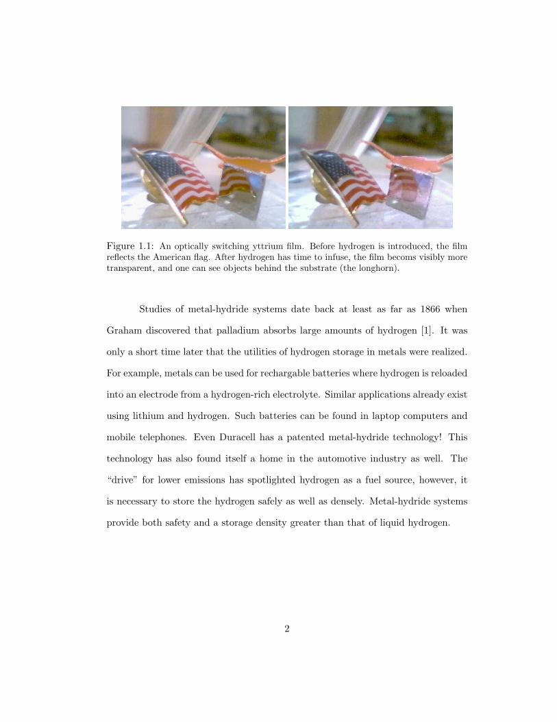
Figure 1.1: An optically switching yttrium film. Before hydrogen is introduced, the filmreflects the American flag. After hydrogen has time to infuse, the film becoms visibly moretransparent, and one can see objects behind the substrate (the longhorn).
Studies of metal-hydride systems date back at least as far as 1866 when
Graham discovered that palladium absorbs large amounts of hydrogen [1]. It was
only a short time later that the utilities of hydrogen storage in metals were realized.
For example, metals can be used for rechargable batteries where hydrogen is reloaded
into an electrode from a hydrogen-rich electrolyte. Similar applications already exist
using lithium and hydrogen. Such batteries can be found in laptop computers and
mobile telephones. Even Duracell has a patented metal-hydride technology! This
technology has also found itself a home in the automotive industry as well. The
“drive” for lower emissions has spotlighted hydrogen as a fuel source, however, it
is necessary to store the hydrogen safely as well as densely. Metal-hydride systems
provide both safety and a storage density greater than that of liquid hydrogen.
2
1.2 Switchable Mirrors
More in line with these studies, hydrogen is able to create an optical gap
in some rare-earth metals such as yttrium and lanthanum. Reversible transitions
between the metallic-mirror and optically transparent-insulator states are possible
by changing the metal’s hydrogen contentover a small range. With such dramatic
switching properties, it may be possible to create energy efficiency devices such as
“smart windows” which act as a mirror to deflect sunlight or as a transparent window
to allow natural lighting. These characteristics can be seen in the 100 nm yttrium
film pictured in Fig. 1.1. Prior to exposure to hydrogen the film reflects an object in
front of it (the American flag), and after exposure, one can see an object behind the
substrate (the longhorn). The residual reflecting properties seen after hydrogenation
are due mostly to the protective capping layer of palladium. The existence of this
quick and reversible optical transition was discovered in yttrium and lanthanum in
1996 by the group of Ronald Griessen at the Vrije University of Amsterdam [2].
The discovery occured while looking into dirty, atomic, metallic hydrogen in a high
pressure diamond anvil cell at low temperatures. However, the earliest signs of this
behavior were actually seen as early as 1977 in the accompanying metal-insulator
transition and in band structure studies [52, 53, 48, 41]. Studies on bulk materials
described the transition as one from shiny metal, at the dihydride phase (MH2;
M = metal), to a dark, unstable powder, in the trihydride (MH3) [17]. Due to
this instability, combined with a lack of film growth capabilities, only more recent
experiments on thin films have observed the drastic change in optical and electrical
properties between these two states, simultaneously. Furthermore, the transition can
3
H2
gas Pd Metal
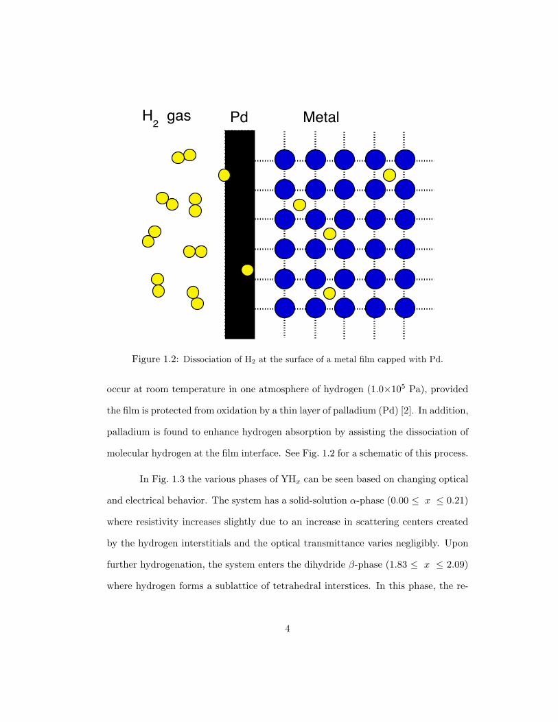
Figure 1.2: Dissociation of H2 at the surface of a metal film capped with Pd.
occur at room temperature in one atmosphere of hydrogen (1.0×10⁵ Pa), provided
the film is protected from oxidation by a thin layer of palladium (Pd) [2]. In addition,
palladium is found to enhance hydrogen absorption by assisting the dissociation of
molecular hydrogen at the film interface. See Fig. 1.2 for a schematic of this process.
In Fig. 1.3 the various phases of YHx can be seen based on changing optical
and electrical behavior. The system has a solid-solution α-phase (0.00 ≤ x ≤ 0.21)
where resistivity increases slightly due to an increase in scattering centers created
by the hydrogen interstitials and the optical transmittance varies negligibly. Upon
further hydrogenation, the system enters the dihydride β-phase (1.83 ≤ x ≤ 2.09)
where hydrogen forms a sublattice of tetrahedral interstices. In this phase, the re-
4
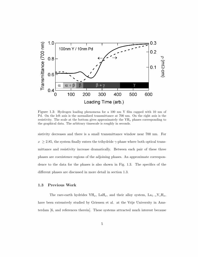
Figure 1.3: Hydrogen loading phenomena for a 100 nm Y film capped with 10 nm ofPd. On the left axis is the normalized transmittance at 700 nm. On the right axis is theresistivity. The scale at the bottom gives approximately the YHx phases corresponding tothe graphical data. The arbitrary timescale is roughly in seconds.
sistivity decreases and there is a small transmittance window near 700 nm. For
x ≥ 2.85, the system finally enters the trihydride γ-phase where both optical trans-
mittance and resistivity increase dramatically. Between each pair of these three
phases are coexistence regions of the adjoining phases. An approximate correspon-
dence to the data for the phases is also shown in Fig. 1.3. The specifics of the
different phases are discussed in more detail in section 1.3.
1.3 Previous Work
The rare-earth hydrides YHx, LaHx, and their alloy system, La1−zYzHx,
have been extensively studied by Griessen et al. at the Vrije University in Ams-
terdam [6, and references therein]. These systems attracted much interest because
5
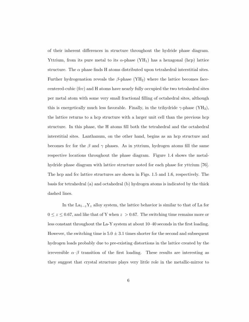
of their inherent differences in structure throughout the hydride phase diagram.
Yttrium, from its pure metal to its α-phase (YH1) has a hexagonal (hcp) lattice
structure. The α phase finds H atoms distributed upon tetrahedral interstitial sites.
Further hydrogenation reveals the β-phase (YH2) where the lattice becomes face-
centered-cubic (fcc) and H atoms have nearly fully occupied the two tetrahedral sites
per metal atom with some very small fractional filling of octahedral sites, although
this is energetically much less favorable. Finally, in the trihydride γ-phase (YH3),
the lattice returns to a hcp structure with a larger unit cell than the previous hcp
structure. In this phase, the H atoms fill both the tetrahedral and the octahedral
interstitial sites. Lanthanum, on the other hand, begins as an hcp structure and
becomes fcc for the β and γ phases. As in yttrium, hydrogen atoms fill the same
respective locations throughout the phase diagram. Figure 1.4 shows the metal-
hydride phase diagram with lattice structure noted for each phase for yttrium [76].
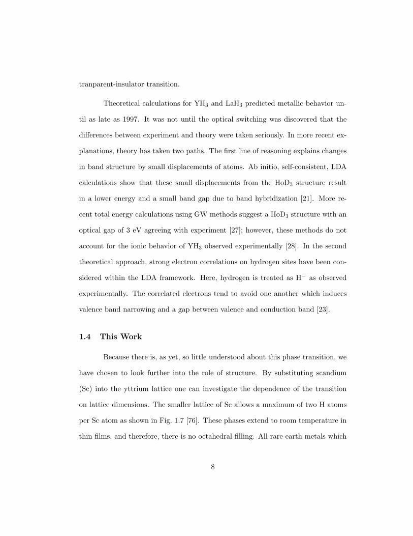
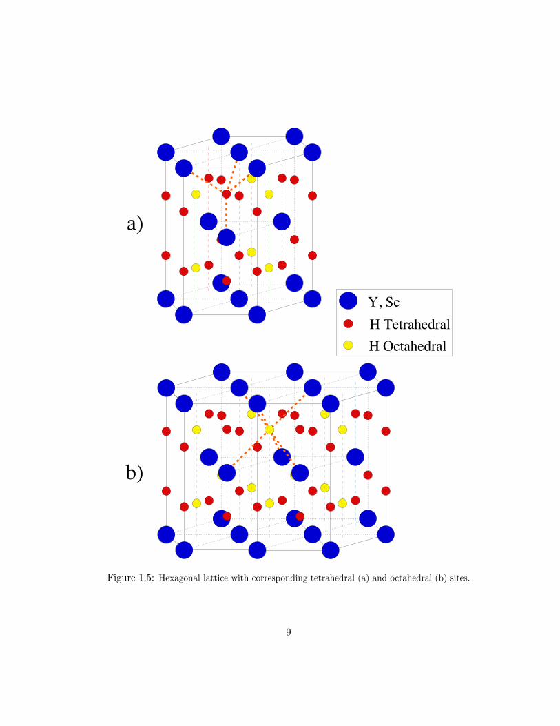
The hcp and fcc lattice structures are shown in Figs. 1.5 and 1.6, respectively. The
basis for tetrahedral (a) and octahedral (b) hydrogen atoms is indicated by the thick
dashed lines.
In the La1−zYz alloy system, the lattice behavior is similar to that of La for
0 ≤ z ≤ 0.67, and like that of Y when z > 0.67. The switching time remains more or
less constant throughout the La-Y system at about 10–40 seconds in the first loading.
However, the switching time is 5.0 ± 3.1 times shorter for the second and subsequent
hydrogen loads probably due to pre-existing distortions in the lattice created by the
irreversible α–β transition of the first loading. These results are interesting as
they suggest that crystal structure plays very little role in the metallic-mirror to
6
Figure 1.4: Hydride structure and phase diagram for Y. There are three distinct phases:α (hcp monohydride), β (fcc dihydride), and γ (hcp trihydride).
7
tranparent-insulator transition.
Theoretical calculations for YH3 and LaH3 predicted metallic behavior un-
til as late as 1997. It was not until the optical switching was discovered that the
differences between experiment and theory were taken seriously. In more recent ex-
planations, theory has taken two paths. The first line of reasoning explains changes
in band structure by small displacements of atoms. Ab initio, self-consistent, LDA
calculations show that these small displacements from the HoD3 structure result
in a lower energy and a small band gap due to band hybridization [21]. More re-
cent total energy calculations using GW methods suggest a HoD3 structure with an
optical gap of 3 eV agreeing with experiment [27]; however, these methods do not
account for the ionic behavior of YH3 observed experimentally [28]. In the second
theoretical approach, strong electron correlations on hydrogen sites have been con-
sidered within the LDA framework. Here, hydrogen is treated as H− as observed
experimentally. The correlated electrons tend to avoid one another which induces
valence band narrowing and a gap between valence and conduction band [23].
1.4 This Work
Because there is, as yet, so little understood about this phase transition, we
have chosen to look further into the role of structure. By substituting scandium
(Sc) into the yttrium lattice one can investigate the dependence of the transition
on lattice dimensions. The smaller lattice of Sc allows a maximum of two H atoms
per Sc atom as shown in Fig. 1.7 [76]. These phases extend to room temperature in
thin films, and therefore, there is no octahedral filling. All rare-earth metals which
8
a)
b)
Y, Sc
H Tetrahedral
H Octahedral
Figure 1.5: Hexagonal lattice with corresponding tetrahedral (a) and octahedral (b) sites.
9
a)
b)
Y, Sc
H Tetrahedral
H Octahedral
Figure 1.6: Face-centered cubic lattice with corresponding tetrahedral (a) and octahedral(b) sites.
10
exhibit the transition of interest form a trihydride. It was believed substitution of
Sc could lead to a structural instability when the lattice is just large enough to store
three H atoms per metal atom. In such strained situations many exotic behaviors
are seen. Indeed, we have found rather interesting results for this alloy system.
Figure 1.8 shows that the entire alloy phase diagram from pure Y to pure Sc forms
at relatively low temperature [76]. Previous research on bulk Y1−zSczHx properties
indicate hydrogen absorption beyond a dihydride composition for alloys of z ≤ 0.4
near 240C [7]. Our results indicate hydrogen concentrations in excess of dihydride
occur for all alloys at room temperature and one atmosphere of hydrogen for thin
films. Also, we observe the most dramatic changes in the transition near z = 0.20.
We discuss these observations in terms of the local structure around interstitial sites
in the alloy.
The poorly understood dynamics of the optical switching properties in Y and
La thin films have initiated this study. Although the technical prospects for these
materials are interesting and should be investigated, the aim of this dissertation is
to aid the understanding of the physics behind the metallic-mirror to transparent-
insulator transition. We have primarily studied the optical and electrical behavior
of the Y1−zSczHx system. These properties are discussed extensively in Chap. 4
after a short comment on the structural analysis from x-ray diffraction in Chap. 3.
A summary and a brief mention of possible future directions for this work appear
in Chap. 5.
11
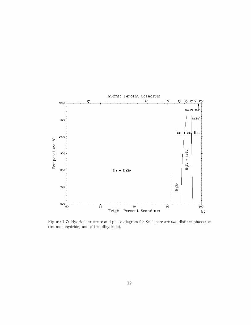
Figure 1.7: Hydride structure and phase diagram for Sc. There are two distinct phases: α(fcc monohydride) and β (fcc dihydride).
12
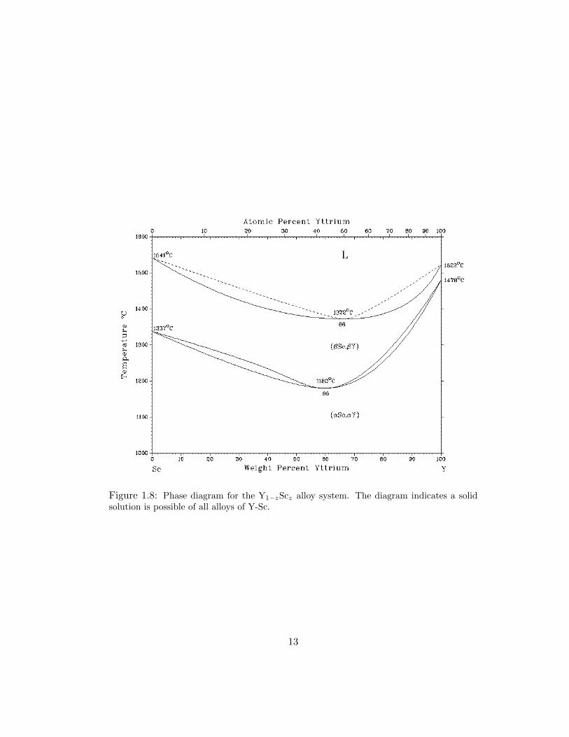
Figure 1.8: Phase diagram for the Y1−zScz alloy system. The diagram indicates a solidsolution is possible of all alloys of Y-Sc.
13
Chapter 2
Experimental
“Ross: So, I just finished this fascinating book. By the year 2030, there’ll be
computers that can carry out the same amount of functions as an actual human
brain. So, theoretically, you could download your thoughts and memories into this
computer and live forever as a machine.
Chandler: And I just realized I can sleep with my eyes open.”
- from Friends on NBC
Various elements of our main experimental techniques are described in this
chapter. Included are sections about sample preparation and characterization using
x-ray diffraction (XRD), optical spectrometry, and ac electrical resistivity (ρ(x) and
ρ(T )).
2.1 Sample Preparation
The thin film sample preparation for this metal-hydride work was performed
in two stages. The active layer metals and alloys were cast into 0.125” diameter rods
from stoichiometric combinations of 99.9% (or better) yttrium (Y) and scandium
(Sc). To do this, the metals were first arc-melted on a water-cooled copper hearth
14
in an under-pressure of ultra-high purity argon (≈ 125 torr below atmosphere).
The actual argon pressure used depended on the fluidity of the alloy melt. For
high surface tension alloys, higher pressures made pulling the melt into a copper
mold easier. The inert argon environment was gettered to remove oxygen using
(99.9% purity) zirconium sponge. To ensure homogeneity, the samples were turned
over and arc melted 3–5 times. The alloy lumps were weighed to ensure that loss
of constituents is less than 0.1%. Palladium (Pd) of 99.95% purity is purchased
commercially in 2 mm diameter rods. The Y-Sc alloys and the palladium were then
cast into rods, also by arc-melting. When these rods became too short for use in
the e-beam evaporators, arc-melting was used to combine several scrap pieces into
one useful rod.
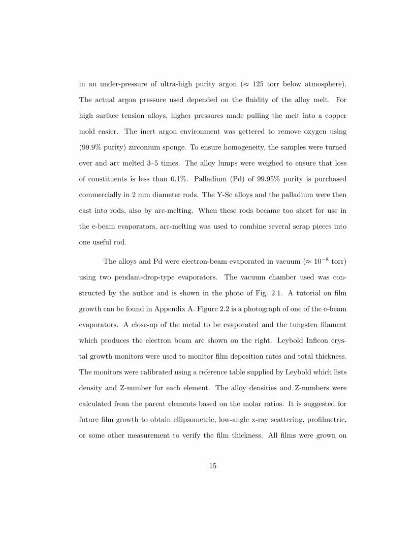
The alloys and Pd were electron-beam evaporated in vacuum (≈ 10−8 torr)
using two pendant-drop-type evaporators. The vacuum chamber used was con-
structed by the author and is shown in the photo of Fig. 2.1. A tutorial on film
growth can be found in Appendix A. Figure 2.2 is a photograph of one of the e-beam
evaporators. A close-up of the metal to be evaporated and the tungsten filament
which produces the electron beam are shown on the right. Leybold Inficon crys-
tal growth monitors were used to monitor film deposition rates and total thickness.
The monitors were calibrated using a reference table supplied by Leybold which lists
density and Z-number for each element. The alloy densities and Z-numbers were
calculated from the parent elements based on the molar ratios. It is suggested for
future film growth to obtain ellipsometric, low-angle x-ray scattering, profilmetric,
or some other measurement to verify the film thickness. All films were grown on
15
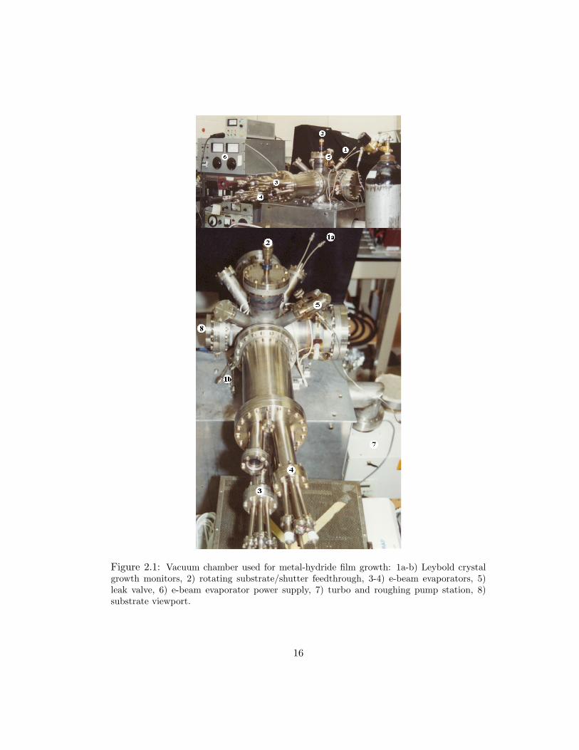
Figure 2.1: Vacuum chamber used for metal-hydride film growth: 1a-b) Leybold crystalgrowth monitors, 2) rotating substrate/shutter feedthrough, 3-4) e-beam evaporators, 5)leak valve, 6) e-beam evaporator power supply, 7) turbo and roughing pump station, 8)substrate viewport.
16
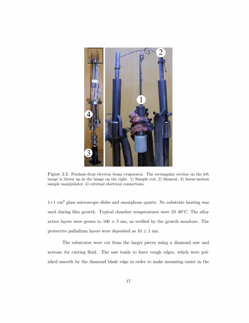
Figure 2.2: Pendant-drop electron beam evaporator. The rectangular section on the leftimage is blown up in the image on the right. 1) Sample rod, 2) filament, 3) linear-motionsample manipulator, 4) external electrical connections.
1×1 cm2 glass microscope slides and amorphous quartz. No substrate heating was
used during film growth. Typical chamber temperatures were 23–30C. The alloy
active layers were grown to 100 ± 5 nm, as verified by the growth monitors. The
protective palladium layers were deposited as 10 ± 1 nm.
The substrates were cut from the larger pieces using a diamond saw and
acetone for cutting fluid. The saw tends to leave rough edges, which were pol-
ished smooth by the diamond blade edge in order to make mounting easier in the
17
spectrometer and low-temperature resistivity probe. Systematic studies have been
performed to achieve the best substrate cleaning procedure [6]. In this study, it
was found that rubbing with fingers is superior to cotton-wool swabs. Ultrasonic
cleaning did not lower particle densities, and, surprisingly, acetone contaminates
substrate surfaces regardless of its initial purity. Conversations with Ben Shoulders
of the Chemistry Department at the University of Texas at Austin suggest that
acetone contains polymers that are easily broken causing them to adhere to surfaces
such as substrates and vacuum chamber interiors. These polymers behave like dirt,
and, therefore, acetone should not be used for cleaning substrates or vacuum com-
ponents. The following procedure has been adopted for these studies and resulted
in long-lasting films which were resistant to peeling.
1. Wash hands with soap.
2. Rub the substrate with Glass PlusTM glass cleaner for 30 seconds with bare
fingers.
3. Remove excess glass cleaner with n-propanol
4. Soak substrates for 10 seconds in n-propanol and rub with bare fingers until
they feel squeaky clean.
5. Spin the substrates dry in a modified coffee grinder spinner.
For film evaporation, the substrates were mounted to a rotating substrate holder
with double-sided tape. This method of adhesion is not the optimal method; how-
ever, silver epoxy, Torr Seal, and two-part epoxy all resulted in substrate breakage
18
d
θθ
2θ
n λ = 2d sin θ
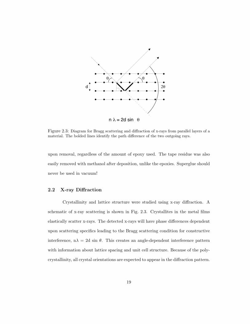
Figure 2.3: Diagram for Bragg scattering and diffraction of x-rays from parallel layers of amaterial. The bolded lines identify the path difference of the two outgoing rays.
upon removal, regardless of the amount of epoxy used. The tape residue was also
easily removed with methanol after deposition, unlike the epoxies. Superglue should
never be used in vacuum!
2.2 X-ray Diffraction
Crystallinity and lattice structure were studied using x-ray diffraction. A
schematic of x-ray scattering is shown in Fig. 2.3. Crystallites in the metal films
elastically scatter x-rays. The detected x-rays will have phase differences dependent
upon scattering specifics leading to the Bragg scattering condition for constructive
interference, nλ = 2d sin θ. This creates an angle-dependent interference pattern
with information about lattice spacing and unit cell structure. Because of the poly-
crystallinity, all crystal orientations are expected to appear in the diffraction pattern.
19
The samples are scanned over the range 2θ = 10–70 at 0.05 increments. Each
angle is integrated for 3–7 seconds. The machines used were Philips (model PW
1720) RIGAKU diffractometers which produce x-rays with λ = 1.540562 A (Cu
Kα2 line). MDI Datascan software was used to control the goniometer (also manu-
factured by Philips). Powder diffraction references for Y, YH2, YH3, Sc, ScH, ScH2,
and Pd were obtained from MDI Jade pattern analysis software [26].
2.3 Optical Spectroscopy
Optical spectra were measured using a Bausch and Lomb Spectronic 20
spectral analyzer shown in Fig. 2.4. This type of spectrometer used a rotating
reflection grating to split light into specific wavelengths as shown in Fig. 2.5. The
spectral bandwidth incident on the sample was 20 nm. The diffraction grating was
the blazed angle variety which consists of stepped edges with angle γ to the normal.
Without the blazed angles the interference peaks would be described by the standard
diffraction grating equation
a sin θm = mλ, (2.1)
for normal incidence, line spacing, a, and θm is the angle to the mth order peak. If
the incoming light is at an oblique angle, θi, this equation is generalized to
a(sin θm − sin θi) = mλ. (2.2)
It follows when θm = θi, the zeroth order peak is observed, however, this is the same
angle for all wavelengths. Therefore, a large amount of reflected intensity is wasted
in an unresolvable region. Use of a blazed angle grating, however, circumvents this
20
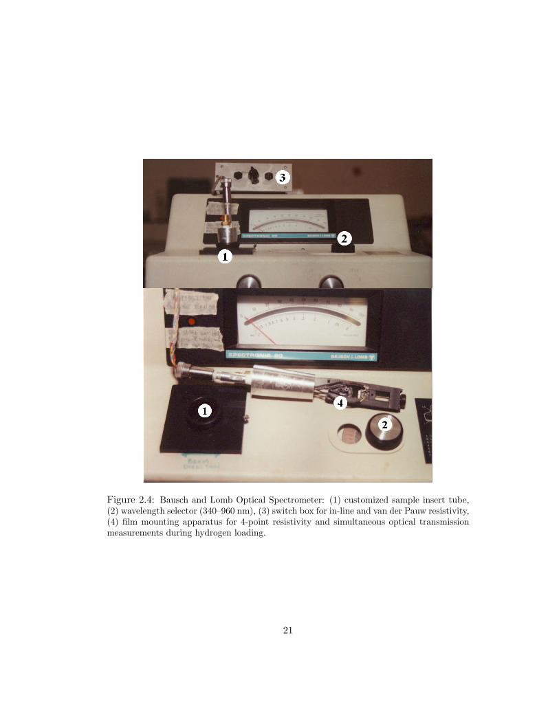
Figure 2.4: Bausch and Lomb Optical Spectrometer: (1) customized sample insert tube,(2) wavelength selector (340–960 nm), (3) switch box for in-line and van der Pauw resistivity,(4) film mounting apparatus for 4-point resistivity and simultaneous optical transmissionmeasurements during hydrogen loading.
21
Reflection GratingDetector Film
White Light From Incandescent Source
Figure 2.5: Schematic of the Bausch & Lomb Spectronic 20 rotating reflection grating.
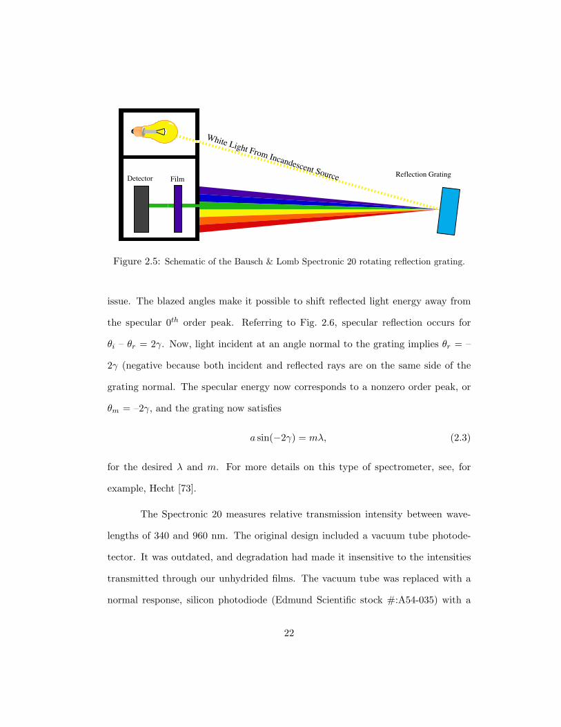
issue. The blazed angles make it possible to shift reflected light energy away from
the specular 0th order peak. Referring to Fig. 2.6, specular reflection occurs for
θi – θr = 2γ. Now, light incident at an angle normal to the grating implies θr = –
2γ (negative because both incident and reflected rays are on the same side of the
grating normal. The specular energy now corresponds to a nonzero order peak, or
θm = –2γ, and the grating now satisfies
a sin(−2γ) = mλ, (2.3)
for the desired λ and m. For more details on this type of spectrometer, see, for
example, Hecht [73].
The Spectronic 20 measures relative transmission intensity between wave-
lengths of 340 and 960 nm. The original design included a vacuum tube photode-
tector. It was outdated, and degradation had made it insensitive to the intensities
transmitted through our unhydrided films. The vacuum tube was replaced with a
normal response, silicon photodiode (Edmund Scientific stock #:A54-035) with a
22
γθ
θ
rotation angle
r
i
Figure 2.6: White light incident on the blaze angle reflection grating is split into constituentcolors, which one can select on the spectrometer based on the angle of the reflection grating.
23
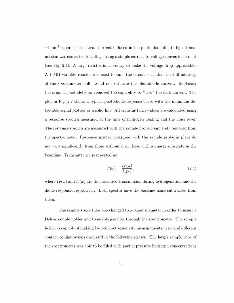
44 mm2 square sensor area. Current induced in the photodiode due to light trans-
mission was converted to voltage using a simple current-to-voltage conversion circuit
(see Fig. 2.7). A large resistor is necessary to make the voltage drop appreciable.
A 1 MΩ variable resistor was used to tune the circuit such that the full intensity
of the spectrometer bulb would not saturate the photodiode current. Replacing
the original photodetector removed the capability to “zero” the dark current. The
plot in Fig. 2.7 shows a typical photodiode response curve with the minimum de-
tectable signal plotted as a solid line. All transmittance values are calculated using
a response spectra measured at the time of hydrogen loading and the noise level.
The response spectra are measured with the sample probe completely removed from
the spectrometer. Response spectra measured with the sample probe in place do
not vary significantly from those without it or those with a quartz substrate in the
beamline. Transmittance is reported as
T (ω) =IT (ω)Io(ω)
, (2.4)
where IT (ω) and Io(ω) are the measured transmission during hydrogenation and the
diode response, respectively. Both spectra have the baseline noise subtracted from
them.
The sample space tube was changed to a larger diameter in order to insert a
Delrin sample holder and to enable gas flow through the spectrometer. The sample
holder is capable of making four-contact resistivity measurements in several different
contact configurations discussed in the following section. The larger sample tube of
the spectrometer was able to be filled with partial pressure hydrogen concentrations
24
-
+
1 M Ω
OP741photodiode
to voltmeter
NC
NC
Vout
+15V
NC
- in
+ in
-15V
OP741
0.4
0.2
0.01000800600400
Wavelength (nm)
Res
pons
e (V
olts
)
Figure 2.7: Current-to-voltage circuit diagram for the photodiode measuring optical trans-mission in the Bausch and Lomb spectrometer. The graph shows a typical photodioderesponse as a function of incident wavelength. The solid line is the baseline due to darkcurrent.
25
to 0.75 torr (≈ 1 mbar or 0.1% hydrogen:argon). This flow control was important for
slowing the hydrogen absorption, and thus, the optical switching rate, so that many
optical spectra could be recorded throughout the transition. Typically, the total
switching time was on the order of 2 hours. The gas flow control was performed
using an MKS Baratron mass flow controller. Hydrogen loading is performed in
1 atm of mixtures of hydrogen in argon with typical flow rates of 10-50 sccm.
2.4 AC Electrical Resistivity
The room temperature resistivity probe was machined from delrin and de-
signed to measure resistivity in an in-line 4-point configuration or by the van der
Pauw method (see Fig. 2.8). Selection between these two configurations was made
by a rotary switch box. The in-line 4-point method (Fig. 2.9) was used exclusively
due to speed and simplicity. In this geometry, resistivity can be calculated directly
from the resistance measured and the geometry of the pins as
ρ =RA
l, (2.5)
where R is the measured resistance, A is the cross-sectional film area (w×h) through
which current flows, and l is the distance between the voltage contacts. Error from
this technique is inherent due to the assumption that l w and difficulty measuring
the sample dimensions. The van der Pauw method requires switching between two
orthogonal configurations shown in Fig. 2.10. Resistivity is calculated as
ρ =πh
ln2R0 + R90
2f(
R0
R90), (2.6)
26
inI
V1
V2
Iout
inI
V1
V2
Iout
0.5 mm
1.0 mm
2.0 mm
4.0 mm
9.0 mm
2.0 mm
1.0 mm
0.5 mm
Figure 2.8: Contact configuration of the room temperature resistivity probe.
27
IinV1
2VoutI
w
lh
Figure 2.9: In-line 4-point contact geometry for ac resistivity measurements. The entiresample represents a 1–2 mm wide strip from a 1 × 1 cm2 film. In this configuration, ρ =Rhw/l.
where f(R0/R90) ≈ 1 for isotropic materials, such as polycrystalline films. This
technique has smaller error and is roughly independent of the sample geometry, how-
ever, it is more difficult to estimate and requires some analysis due to the function
f .
The sample contacts were gold-coated pogo sticks mounted into the sample
holder with spacings shown in Fig. 2.8. The films were sectioned using a diamond-
tipped scribe such that a 1–2 mm width area of the film was used for resistivity and
the other 8–9 mm was used for spectroscopy. Contact resistances were monitored
and kept below 1 Ω. A Linear Research LR-400 ac resistance bridge was used to
record resistance of the films. Use of an ac resistance bridge eliminates effects due
to temperature gradients and high contact resistances.
Temperature-dependent resistivity measurements were subsequently made
28
Iin
V1
2V
outI
Iin
V1 2V
outI
Figure 2.10: The van der Pauw technique for 4-contact ac resistivity measurements.
inI
V1
V2
Iout Pogo Sticks
Sample(scribed)
PositioningScrew
MacorGuide
Copper Base
RuO Thermometer
Figure 2.11: Sample mount for temperature-dependent in-line 4-contact resistivity mea-surements on films.
29
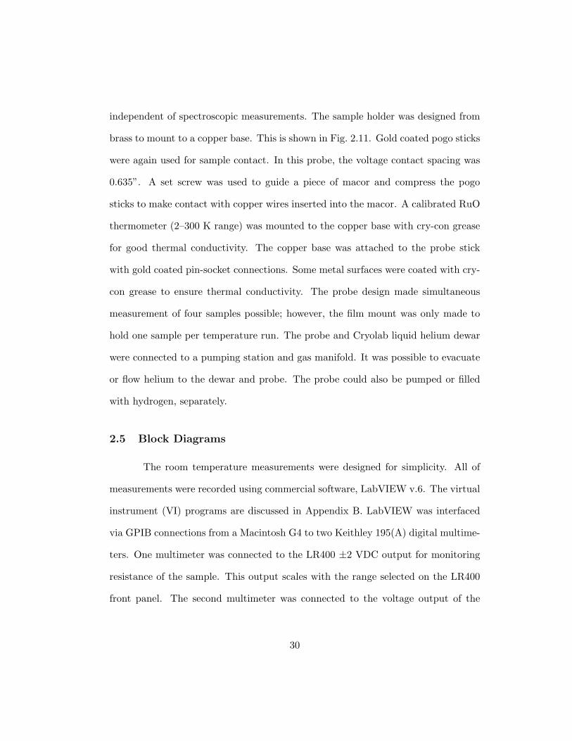
independent of spectroscopic measurements. The sample holder was designed from
brass to mount to a copper base. This is shown in Fig. 2.11. Gold coated pogo sticks
were again used for sample contact. In this probe, the voltage contact spacing was
0.635”. A set screw was used to guide a piece of macor and compress the pogo
sticks to make contact with copper wires inserted into the macor. A calibrated RuO
thermometer (2–300 K range) was mounted to the copper base with cry-con grease
for good thermal conductivity. The copper base was attached to the probe stick
with gold coated pin-socket connections. Some metal surfaces were coated with cry-
con grease to ensure thermal conductivity. The probe design made simultaneous
measurement of four samples possible; however, the film mount was only made to
hold one sample per temperature run. The probe and Cryolab liquid helium dewar
were connected to a pumping station and gas manifold. It was possible to evacuate
or flow helium to the dewar and probe. The probe could also be pumped or filled
with hydrogen, separately.
2.5 Block Diagrams
The room temperature measurements were designed for simplicity. All of
measurements were recorded using commercial software, LabVIEW v.6. The virtual
instrument (VI) programs are discussed in Appendix B. LabVIEW was interfaced
via GPIB connections from a Macintosh G4 to two Keithley 195(A) digital multime-
ters. One multimeter was connected to the LR400 ±2 VDC output for monitoring
resistance of the sample. This output scales with the range selected on the LR400
front panel. The second multimeter was connected to the voltage output of the
30
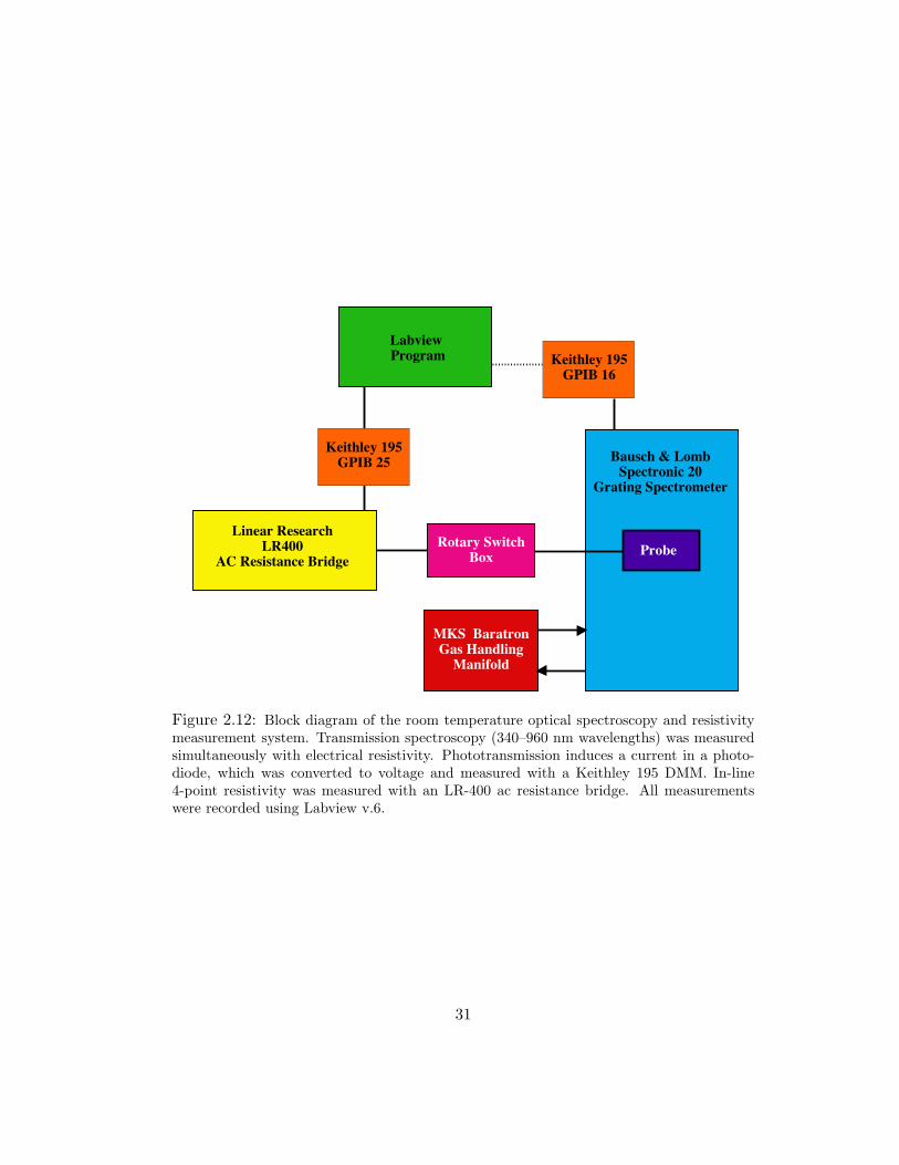
Labview Program
Linear ResearchLR400
AC Resistance BridgeRotary Switch
Box
Bausch & LombSpectronic 20
Grating Spectrometer
Probe
MKS BaratronGas Handling
Manifold
Keithley 195GPIB 16
Keithley 195GPIB 25
Figure 2.12: Block diagram of the room temperature optical spectroscopy and resistivitymeasurement system. Transmission spectroscopy (340–960 nm wavelengths) was measuredsimultaneously with electrical resistivity. Phototransmission induces a current in a photo-diode, which was converted to voltage and measured with a Keithley 195 DMM. In-line4-point resistivity was measured with an LR-400 ac resistance bridge. All measurementswere recorded using Labview v.6.
31
Labview Program
Linear ResearchLR400
AC Resistance BridgeSimple Probe
Box
Probe
Pump Station & Gas Manifold
Cryofab Liquid Helium Dewar
Keithley 195GPIB 25
Keithley 195GPIB 16
Figure 2.13: Block diagram of the temperature dependent resistivity measurement system.In-line 4-point resistivity was measured with an LR-400 ac resistance bridge and output toa Keithley 195A DMM. Temperature was monitored with a calibrated RuO thermometerconnected in a 4-contact geometry to a Keithley 195 DMM. All measurements are recordedusing LabVIEW v.6.
current-to-voltage circuit of Fig. 2.7. The rotary switch box (discussed in the pre-
vious section) was used to select between the possible resistivity pin configurations.
Gas flow connections were made with brass and stainless steel Swagelock or VCR fit-
tings. Plastic and stainless steel gas conduits directed gas through the spectrometer.
Figure 2.12 shows the block diagram of the room temperature experiment.
For temperature dependent resistivity measurements, a similar LabVIEW
VI was created (also discussed in Appendix B). One multimeter monitored film
32

resistance, while the second measured the RuO thermometer resistance. The ther-
mometer resistance was converted to temperature within the VI. Both the dewar
and the probe were connected to a pumping station and gas flow manifold.
33
Chapter 3
Structural Analysis
“Well, we talk about physics, the properties of physics...”
- Brian in The Breakfast Club
This study is based on lattice size effects on the switchable mirror transition
in yttrium. X-ray diffraction, as discussed in the previous chapter, is a powerful tool
for detailing both structure and lattice dimensions upon substitution of Sc into the
Y lattice. The following is an analysis of x-ray diffraction for both the as-deposited
(not hydrided) and unloaded (dihydride) films.
3.1 As-Deposited Films
In a perfect world, where delta functions truly exist, the Bragg condition
would result in sharp, delta-function peaks at angles of constructive interference.
Figure 3.1, shows the expected diffraction patterns for hcp Y, hcp Sc, and fcc Pd.
Also shown in Fig. 3.1 is the measured diffraction pattern for three as-deposited
alloys. The low intensities are typical of polycrystalline thin films. A broad amor-
phous peak near 20 has been removed from the data. Immediately obvious is the
partial c-axis ordering in our films. In most alloys, the only observable peaks are
the (100), (002), and (101); in the measured data, the (100) and (002) peaks can
34
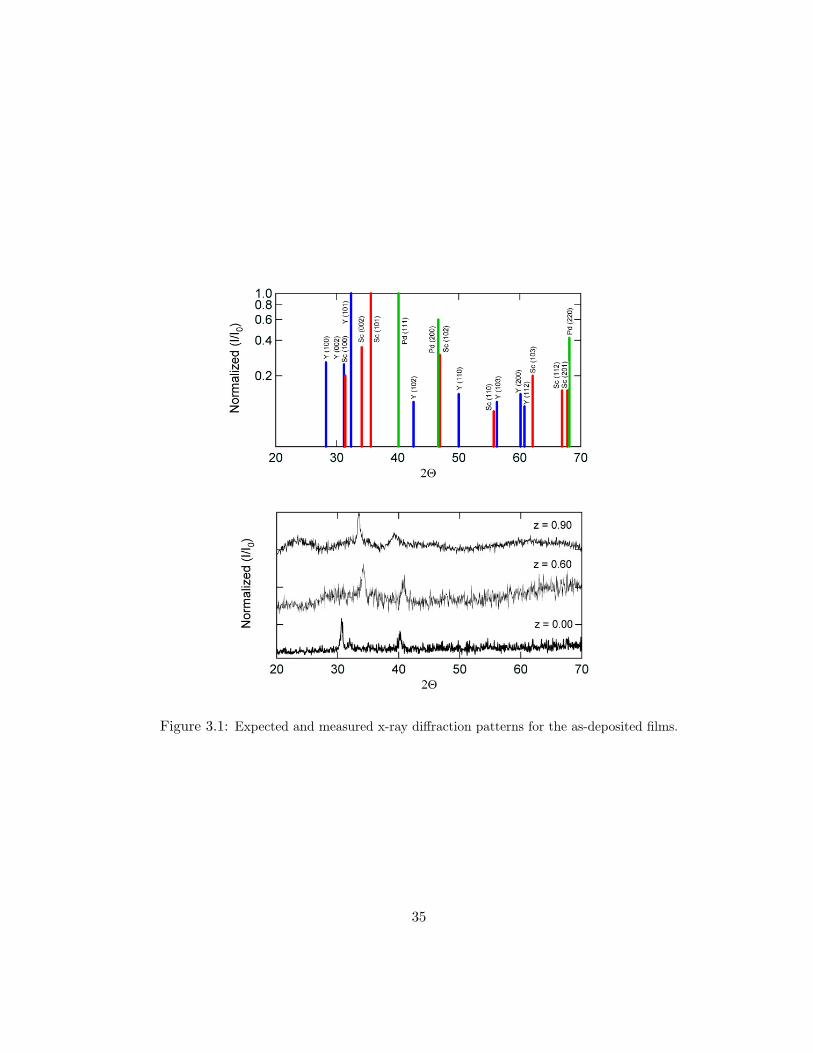
Figure 3.1: Expected and measured x-ray diffraction patterns for the as-deposited films.
35
be observed near 28 and just above 30, respectively. The (101) reflection is found
as a shoulder on the right of the (002) peak. The peak near 2θ = 40 corresponds
to Pd (111). From these, we obtain the alloy composition dependence of the lattice
constants a and c, shown in Fig. 3.2. The trend is a nearly linear decrease in both
lattice parameters with increasing z. The resulting total decrease in cell volume
(Vcell = 3√
3a2c/2) is ∼ 38% from z = 0 to z = 1.
For z ≤ 0.20, we find larger cell parameters than expected. This is due to
hydrogen incorporation during evaporation. By linearly fitting literature values of
a and c of YHx for 0 ≤ x ≤ 0.3, we calculate an initial hydrogen concentration of
x = 0.30 ± 0.05 [15]. This value is larger than 0.21, the maximum H concentration
for the solid-solution α-phase, which implies existence of a mixed phase of hexagonal
YHε (with δ ≤ 0.21) and cubic YH2−δ. In addition, the hydrogen incorporation
varies with each alloy which leads to the deviation from the expected linear behavior.
Electron diffraction studies by Curzon and Singh report that films with thickness
less than or equal to 100 nm have significant dihydride formation when prepared in
≈ 10−7 torr. The hydrogen concentration decreases as a function of film thickness
[48].
For z > 0.20, the resulting lattice is smaller than expected possibly due to
the presence of the cubic ScH phase. The Sc hcp (100) and (002) reflections have
close angular correspondence to the fcc (111) and (100) ones, respectively. These
films, grown on room temperature substrates, have very small grains. For example,
an angular width of ∼ 1 corresponds to a particle size of 0.1 µm [75]. This, coupled
with the high hydrogen content, causes the XRD peak widths to be on the order of
36
6
5
4
3
Latti
ce S
paci
ng (
Å)
1.00.80.60.40.20.0
Scandium Concentration, z
Figure 3.2: Unit cell lattice parameters, a and c, as a function of Sc concentration, z, forthe hcp as-deposited films. The trend is nearly linear, as expected, with some deviationsdue to hydrogen incorporation during film growth and small grain size.
the separation of the peaks of these two phases (1–2). This causes unidentifiable
overlap of the two phases.
3.2 Dihydride Films
Films which have been loaded one or more times were also evaluated. The
expected and measured XRD patterns for polycrystalline fcc YH2, fcc ScH2, and fcc
Pd are shown in Fig. 3.3. As expected, the predominant peak is the fcc (111), which
corresponds to the hcp (001) in the unhydrided Y and Sc metals. The measured
unit cell parameter, a, is 5.197 A for YH2 and 4.768 A for ScH2. These values
are within 1% of the expected values [26]. One would then predict the alloy lattice
parameters to fall on a line between these two values. The data in Fig. 3.4 indicate
smaller than expected values for a in the range 0.20 ≤ z ≤ 0.60. The arrow on
the z = 0.60 data of FIg. 3.3 indicates a small peak corresponding to YH2 (111).
37
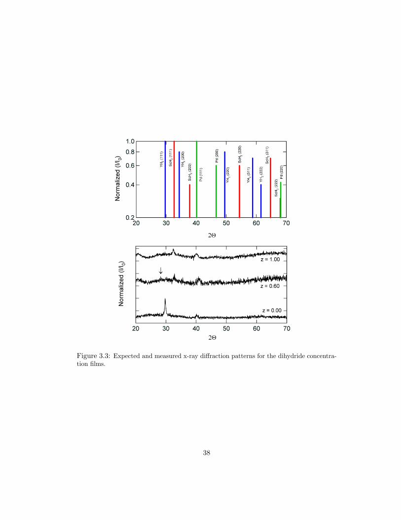
Figure 3.3: Expected and measured x-ray diffraction patterns for the dihydride concentra-tion films.
38
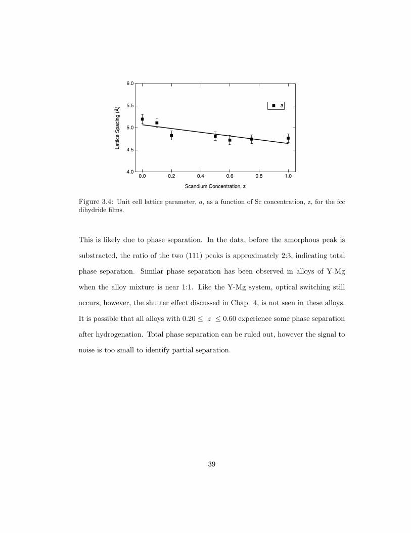
6.0
5.5
5.0
4.5
4.0
Latti
ce S
paci
ng (
Å)
1.00.80.60.40.20.0
Scandium Concentration, z
a
Figure 3.4: Unit cell lattice parameter, a, as a function of Sc concentration, z, for the fccdihydride films.
This is likely due to phase separation. In the data, before the amorphous peak is
substracted, the ratio of the two (111) peaks is approximately 2:3, indicating total
phase separation. Similar phase separation has been observed in alloys of Y-Mg
when the alloy mixture is near 1:1. Like the Y-Mg system, optical switching still
occurs, however, the shutter effect discussed in Chap. 4, is not seen in these alloys.
It is possible that all alloys with 0.20 ≤ z ≤ 0.60 experience some phase separation
after hydrogenation. Total phase separation can be ruled out, however the signal to
noise is too small to identify partial separation.
39
Chapter 4
Results and Analysis
“Fats, man, let me tell you my story man...”
- Gary in Weird Science
4.1 Introduction
The reflecting metal to transparent insulator transition is dependent on for-
mation of a trihydride phase in rare-earth metals. The transition occurs between the
dihydride and trihydride concentrations [2]. It has been observed that trihydride-
forming alloys (e.g., La1−zYz) undergo different switching mechanisms than combi-
nations of trihydride- and dihydride-forming metals (e.g., Mg0.50Y0.50), where the
latter phase separate [24, 29, 31]. In the MgzY1−zHx system, disproportionation
creates a mixture of YH2 and metallic Mg. Further hydrogenation forms insulat-
ing MgH2 and YH3. The magnesium behaves as a microscopic shutter, enhancing
reflectivity in the metallic state and increasing the optical gap in the transparent
state. The result is a switchable mirror with large hydride transmittance over the
entire optical spectrum.
Scandium also maximally forms a dihydride. For this reason, Sc does not
undergo a phase transition from a metallic-mirror to a transparent-insulator. How-
40
ever, yttrium and scandium are chemically very similar with d1s2 valence electrons,
as reflected in the bulk phase diagram of Chap. 1. Optical transmission spectroscopy
of the Y1−zSczHx alloys reveals that the optical gap seen in YH3−δ is strongly sup-
pressed for scandium concentrations of 20% and greater. For alloys with greater
than twenty percent Sc, dihydride transmittance is observed as in the YHx and
La1−zYzHx systems [2, 24]. Electrical properties also exhibit a transition from insu-
lating to metallic as a function of Sc concentration. In addition there is an interesting
metal-insulator transition observed between z = 0.00 and z = 0.10.
In this chapter details of the optical transmittance and electrical resistivity
are discussed. Disproportionation, discussed in the previous chapter, elucidates
some of the observed behavior.
4.2 Optical Spectroscopy Results
We have performed optical transmittance spectroscopy on the alloy system
Y1−zSczHx over the range 340–960 nm as a function of hydrogen content, x. Mea-
surements on the alloys with z ≤ 0.10 show dramatic optical switching properties
commensurate with previous results for YHx [4]. Figure 4.1 exhibits optical spec-
tra (uncorrected for the Pd overlayer) as a function of hydrogen loading time for
YHx and Y0.90Sc0.10Hx. The first hydrogen loading results in a transmittance for
YHx and Y0.90Sc0.10Hx of 0.11 and 0.14, respectively. Although the maximum
transmittance for z = 0.10 is slightly larger than for z = 0.00, the z = 0.10 alloy
has some transmittance before hydrogen is introduced. This low-hydrogen content
transmittance is echoed in the resistivty data and will be discussed more thoroughly
41
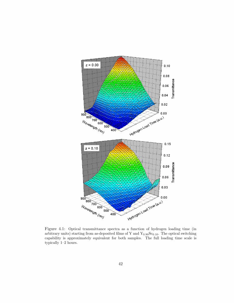
Figure 4.1: Optical transmittance spectra as a function of hydrogen loading time (inarbitrary units) starting from as-deposited films of Y and Y0.90Sc0.10. The optical switchingcapability is approximately equivalent for both samples. The full loading time scale istypically 1–2 hours.
42
Figure 4.2: Optical transmittance spectra as a function of hydrogen loading time (inarbitrary units) starting from as-deposited films Y0.80Sc0.20 and Sc. The vertical axis isscaled to that of the z = 0.00 and z = 0.10 samples. The loss of optical switching capabilityis evident. The full loading time scale is typically 1–2 hours.
43
later. The change in transmittance from as-deposited to fully hydrogenated is ap-
proximately the same for both of these alloys, ∆T ≈ 0.10. We find that for z ≥ 0.20
(Fig. 4.2) the trihydride transmittance is heavily suppressed. The reduction in fully
loaded transmittance is a factor of 3 for z = 0.20 and a factor of 10 for z = 1.00.
Because the real interest is in the optical transition region, it is fortunate
that these alloys form stable dihydrides. The films are allowed to desorb hydro-
gen in flowing argon or in air for approximately 24 hours after the initial hydro-
gen loading; the resulting material is a stable phase very near the dihydride state
(Y1−zSczH2±δ). This state can be verified by observing the well-known dihydride
transmission peak seen in the initial spectrum near λ = 700 nm [2, 4]. Interestingly,
the z = 0.10 exhibits no dihydride transmittance maximum; however, the film does
exhibit reversible switching properties similar to yttrium. If one looks at the change
in transmittance between the dihydride and fully hydrogenated state, the loss of
optical switching is even more apparent than in as-deposited spectra. The spectra
in Fig. 4.3 are for the z = 0.00 and z = 0.10 alloys. The change in transmittance
between dihydride and trihydride is a factor of 6 in the z = 0.00 film and a factor
of 2.3 in the z = 0.10 film. We believe the z = 0.10 films form a stable hydride
with x > 2, explaining the lack of dihydride transparency peak. It can be seen in
Fig. 4.4 that the transmittance increase for x > 2 in the z = 0.20 and z = 1.00
films is 2.3 and 1.7, respectively. Other alloys with z ≥ 0.20 exhibit qualitatively
similar transmittance spectra to those of Figs. 4.2 and 4.4. For films with z = 0.40
(Fig. 4.5), the transmittance is trihydride-like, with a maximum at the highest mea-
sured wavelength (λ = 960 nm). This is consistent the phase separation seen in
44
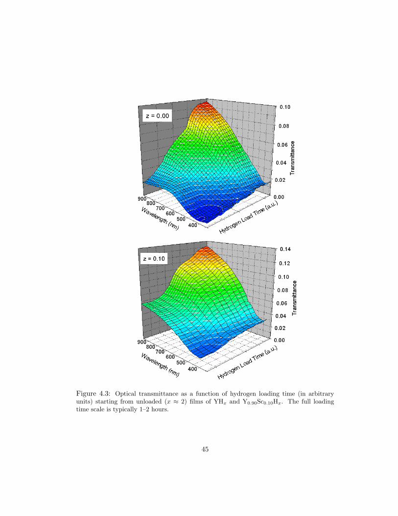
Figure 4.3: Optical transmittance as a function of hydrogen loading time (in arbitraryunits) starting from unloaded (x ≈ 2) films of YHx and Y0.90Sc0.10Hx. The full loadingtime scale is typically 1–2 hours.
45
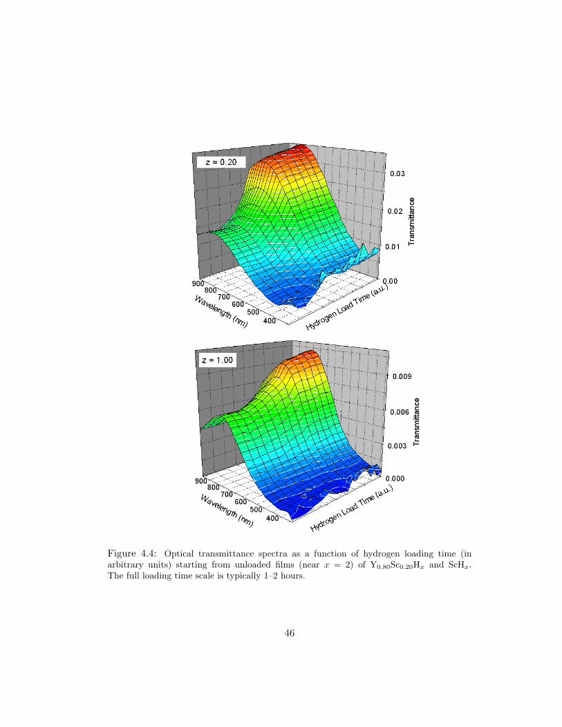
Figure 4.4: Optical transmittance spectra as a function of hydrogen loading time (inarbitrary units) starting from unloaded films (near x = 2) of Y0.80Sc0.20Hx and ScHx.The full loading time scale is typically 1–2 hours.
46
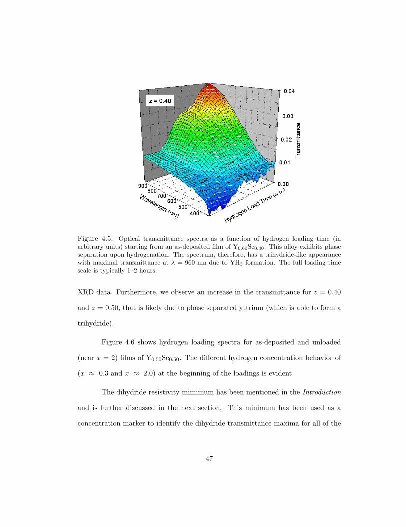
Figure 4.5: Optical transmittance spectra as a function of hydrogen loading time (inarbitrary units) starting from an as-deposited film of Y0.60Sc0.40. This alloy exhibits phaseseparation upon hydrogenation. The spectrum, therefore, has a trihydride-like appearancewith maximal transmittance at λ = 960 nm due to YH3 formation. The full loading timescale is typically 1–2 hours.
XRD data. Furthermore, we observe an increase in the transmittance for z = 0.40
and z = 0.50, that is likely due to phase separated yttrium (which is able to form a
trihydride).
Figure 4.6 shows hydrogen loading spectra for as-deposited and unloaded
(near x = 2) films of Y0.50Sc0.50. The different hydrogen concentration behavior of
(x ≈ 0.3 and x ≈ 2.0) at the beginning of the loadings is evident.
The dihydride resistivity mimimum has been mentioned in the Introduction
and is further discussed in the next section. This minimum has been used as a
concentration marker to identify the dihydride transmittance maxima for all of the
47
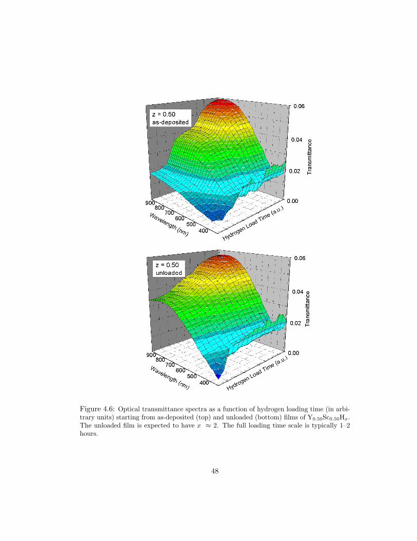
Figure 4.6: Optical transmittance spectra as a function of hydrogen loading time (in arbi-trary units) starting from as-deposited (top) and unloaded (bottom) films of Y0.50Sc0.50Hx.The unloaded film is expected to have x ≈ 2. The full loading time scale is typically 1–2hours.
48
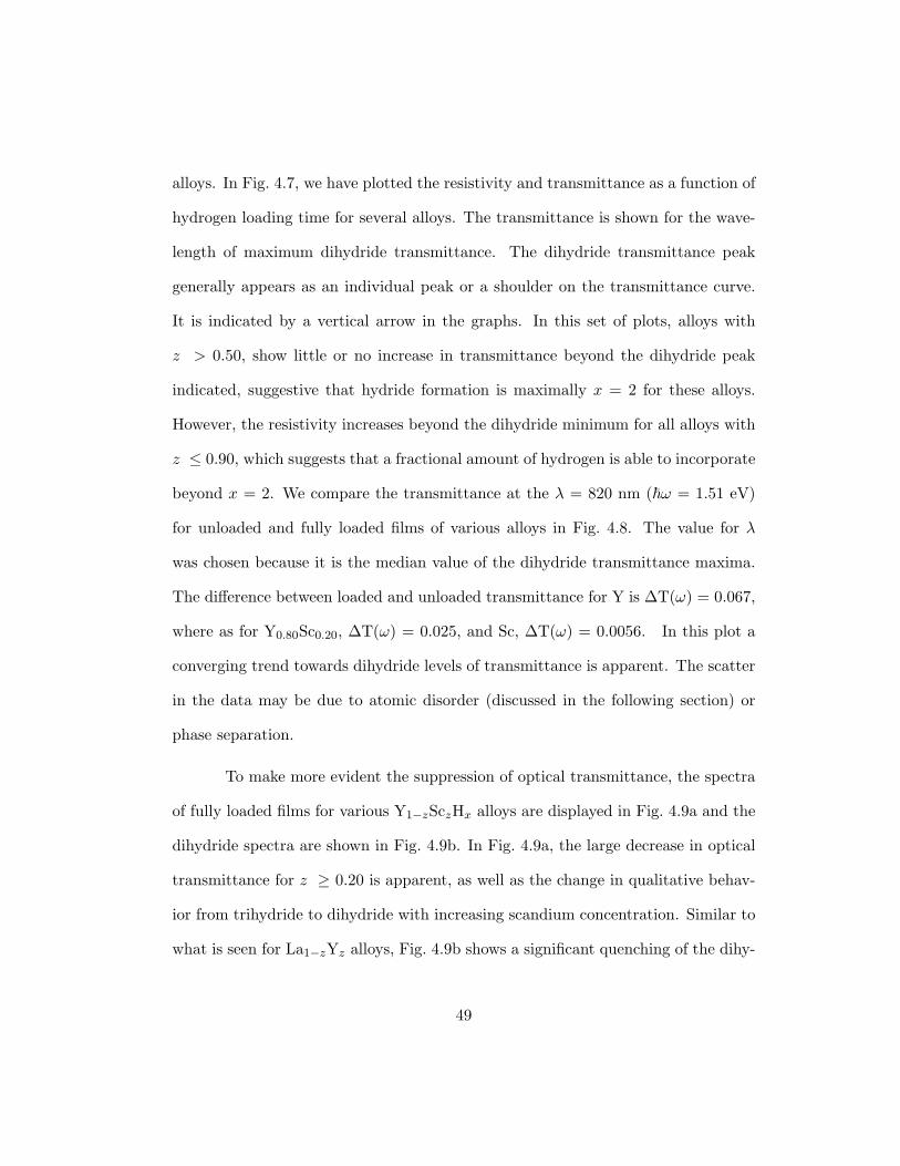
alloys. In Fig. 4.7, we have plotted the resistivity and transmittance as a function of
hydrogen loading time for several alloys. The transmittance is shown for the wave-
length of maximum dihydride transmittance. The dihydride transmittance peak
generally appears as an individual peak or a shoulder on the transmittance curve.
It is indicated by a vertical arrow in the graphs. In this set of plots, alloys with
z > 0.50, show little or no increase in transmittance beyond the dihydride peak
indicated, suggestive that hydride formation is maximally x = 2 for these alloys.
However, the resistivity increases beyond the dihydride minimum for all alloys with
z ≤ 0.90, which suggests that a fractional amount of hydrogen is able to incorporate
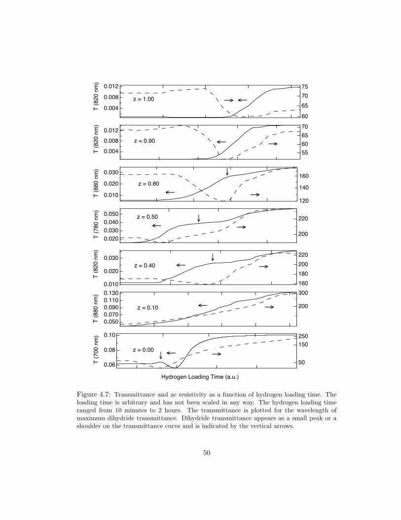
beyond x = 2. We compare the transmittance at the λ = 820 nm (ω = 1.51 eV)
for unloaded and fully loaded films of various alloys in Fig. 4.8. The value for λ
was chosen because it is the median value of the dihydride transmittance maxima.
The difference between loaded and unloaded transmittance for Y is ∆T(ω) = 0.067,
where as for Y0.80Sc0.20, ∆T(ω) = 0.025, and Sc, ∆T(ω) = 0.0056. In this plot a
converging trend towards dihydride levels of transmittance is apparent. The scatter
in the data may be due to atomic disorder (discussed in the following section) or
phase separation.
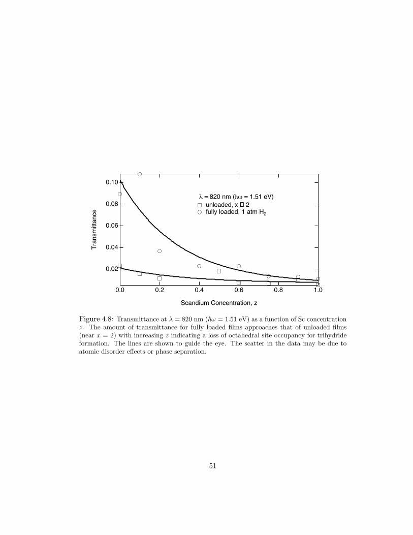
To make more evident the suppression of optical transmittance, the spectra
of fully loaded films for various Y1−zSczHx alloys are displayed in Fig. 4.9a and the
dihydride spectra are shown in Fig. 4.9b. In Fig. 4.9a, the large decrease in optical
transmittance for z ≥ 0.20 is apparent, as well as the change in qualitative behav-
ior from trihydride to dihydride with increasing scandium concentration. Similar to
what is seen for La1−zYz alloys, Fig. 4.9b shows a significant quenching of the dihy-
49
0.012
0.008
0.004T (
820
nm)
75
70
65
60
z = 1.00 ←
←
0.012
0.008
0.004T (
820
nm) 70
65
60
55
z = 0.90 ←←
0.030
0.020
0.010T (
880
nm)
160
140
120
z = 0.80
← ←
↓
0.0500.0400.0300.020T
(78
0 nm
)
220
200
z = 0.50
← ←↓
0.030
0.020
0.010
T (
820
nm)
220
200
180
160
z = 0.40
←←↓
0.1300.1100.0900.0700.050T
(88
0 nm
) 300
200 z = 0.10 ← ←
0.10
0.08
0.06T (
700
nm) 250
150
50
z = 0.00 ← ←
↓
Hydrogen Loading Time (a.u.)
Figure 4.7: Transmittance and ac resistivity as a function of hydrogen loading time. Theloading time is arbitrary and has not been scaled in any way. The hydrogen loading timeranged from 10 minutes to 2 hours. The transmittance is plotted for the wavelength ofmaximum dihydride transmittance. Dihydride transmittance appears as a small peak or ashoulder on the transmittance curve and is indicated by the vertical arrows.
50
0.10
0.08
0.06
0.04
0.02
Tra
nsm
ittan
ce
1.00.80.60.40.20.0
Scandium Concentration, z
λ = 820 nm (hω = 1.51 eV)unloaded, x 2fully loaded, 1 atm H2
Figure 4.8: Transmittance at λ = 820 nm (ω = 1.51 eV) as a function of Sc concentrationz. The amount of transmittance for fully loaded films approaches that of unloaded films(near x = 2) with increasing z indicating a loss of octahedral site occupancy for trihydrideformation. The lines are shown to guide the eye. The scatter in the data may be due toatomic disorder effects or phase separation.
51
Figure 4.9: (a) Fully hydrogen loaded and (b) unloaded (near x = 2) film optical spectrashowing transmittance maxima dependence on alloy composition.
52
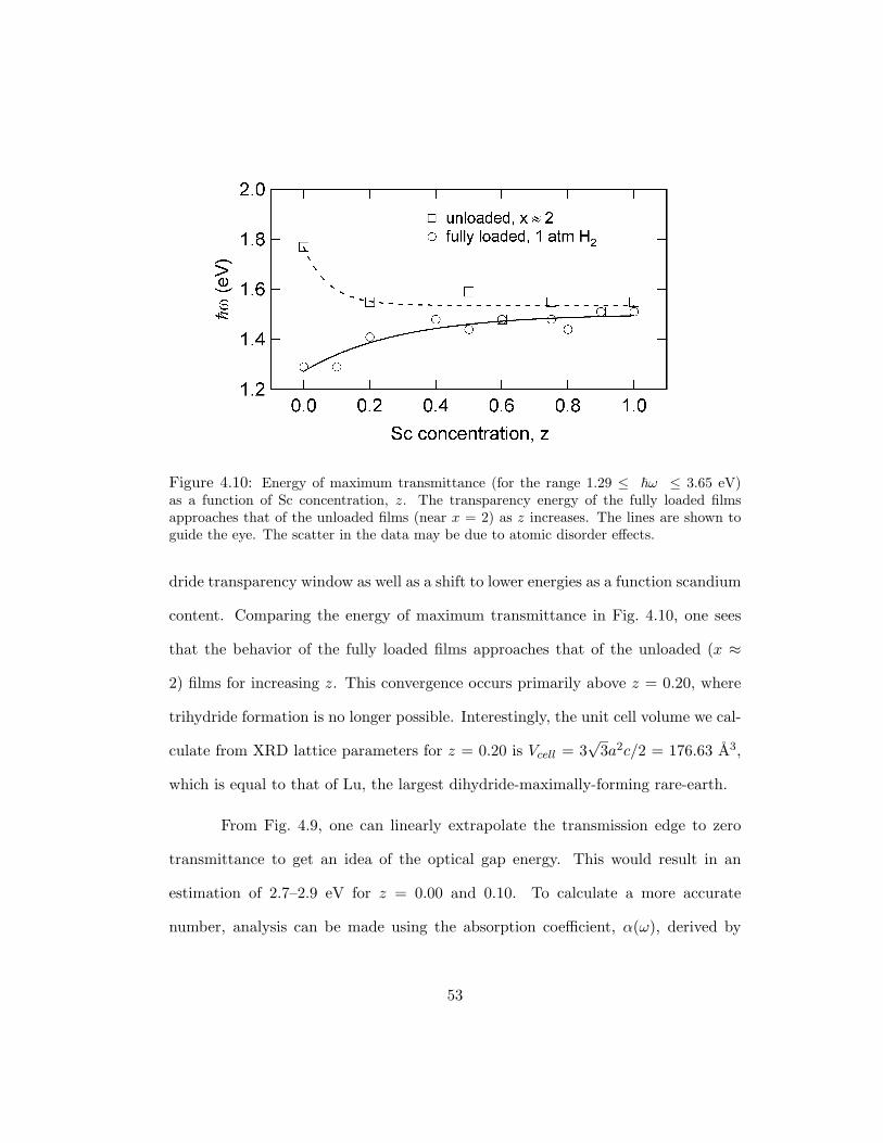
Figure 4.10: Energy of maximum transmittance (for the range 1.29 ≤ ω ≤ 3.65 eV)as a function of Sc concentration, z. The transparency energy of the fully loaded filmsapproaches that of the unloaded films (near x = 2) as z increases. The lines are shown toguide the eye. The scatter in the data may be due to atomic disorder effects.
dride transparency window as well as a shift to lower energies as a function scandium
content. Comparing the energy of maximum transmittance in Fig. 4.10, one sees
that the behavior of the fully loaded films approaches that of the unloaded (x ≈
2) films for increasing z. This convergence occurs primarily above z = 0.20, where
trihydride formation is no longer possible. Interestingly, the unit cell volume we cal-
culate from XRD lattice parameters for z = 0.20 is Vcell = 3√
3a2c/2 = 176.63 A3,
which is equal to that of Lu, the largest dihydride-maximally-forming rare-earth.
From Fig. 4.9, one can linearly extrapolate the transmission edge to zero
transmittance to get an idea of the optical gap energy. This would result in an
estimation of 2.7–2.9 eV for z = 0.00 and 0.10. To calculate a more accurate
number, analysis can be made using the absorption coefficient, α(ω), derived by
53
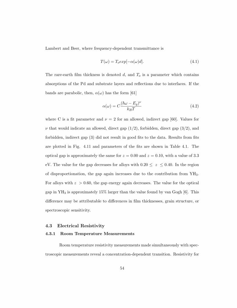
Lambert and Beer, where frequency-dependent transmittance is
T (ω) = Toexp[−α(ω)d]. (4.1)
The rare-earth film thickness is denoted d, and To is a parameter which contains
absorptions of the Pd and substrate layers and reflections due to interfaces. If the
bands are parabolic, then, α(ω) has the form [61]
α(ω) = C(ω − Eg)ν
kBT(4.2)
where C is a fit parameter and ν = 2 for an allowed, indirect gap [60]. Values for
ν that would indicate an allowed, direct gap (1/2), forbidden, direct gap (3/2), and
forbidden, indirect gap (3) did not result in good fits to the data. Results from fits
are plotted in Fig. 4.11 and parameters of the fits are shown in Table 4.1. The
optical gap is approximately the same for z = 0.00 and z = 0.10, with a value of 3.3
eV. The value for the gap decreases for alloys with 0.20 ≤ z ≤ 0.40. In the region
of disproportionation, the gap again increases due to the contribution from YH3.
For alloys with z > 0.60, the gap energy again decreases. The value for the optical
gap in YH3 is approximately 15% larger than the value found by van Gogh [6]. This
difference may be attributable to differences in film thicknesses, grain structure, or
spectroscopic sensitivity.
4.3 Electrical Resistivity
4.3.1 Room Temperature Measurements
Room temperature resistivity measurements made simultaneously with spec-
troscopic measurements reveal a concentration-dependent transition. Resistivity for
54
Figure 4.11: Lambert-Beer fits to the transmission edge.
Optical Transmission Edge Fit Parametersz To C Eg (eV) χ2
0.00 1.71±0.06×10⁻² -6.34±0.16×10⁻⁵ 3.25±0.03 6.02×10⁻⁶
0.10 2.00±0.04×10⁻² -8.07±0.92×10⁻⁴ 3.32±0.12 4.59×10⁻⁵
0.20 7.71±0.80×10⁻³ -4.50±0.30×10⁻⁴ 2.90±0.06 2.04×10⁻⁶
0.60 3.81±0.92×10⁻³ -1.84±0.15×10⁻⁴ 3.28±0.10 2.91×10⁻⁷
1.00 1.19±0.11×10⁻³ -3.72±0.20×10⁻⁴ 2.42±0.02 4.68×10⁻⁷
Table 4.1: Fit parameters from the Lambert-Beer model of the transmission edge forY1−zSczH3−δ.
55
several alloys is plotted in Fig. 4.12. Assuming the two-layer films act as parallel
resistors of rare-earth and palladium, RRE/Pd = RRE ·RPd/(RRE+RPd), we are able
to extract the rare-earth layer resistivity. We measured the resistivity of Pd to be
27–29 µΩ·cm, for all hydrogen concentrations. The resistivity calculated for yttrium
is ρ ≈ 73 µΩ·cm, and for Sc, ρ ≈ 91 µΩ·cm. These values are larger than bulk
literature values likely due to lattice defects, small grain size, and the deposition-
incorporated hydrogen mentioned previously. For yttrium, bulk resistivity has been
reported as 59 µΩ·cm [54], and scandium bulk resistivity is 52–70 µΩ·cm, depending
on purity [54, 44]. As the scandium content is increased the metal to insulator tran-
sition that occurs between the dihydride and fully hydrogenated phases decreases
until, in scandium, the resistivity remains at the dihydride minimum. This is to be
expected, since yttrium was previously known to have a metal to insulator transition
for this range, while scandium maximally incorporates only two hydrogen per scan-
dium atom. Due to the similarities in electronic structure with yttrium, one would
expect ScH2 to be more metallic than pure Sc. Our measurements and literature
support this expectation [17, 43, 44]. Again assuming the parallel resistance model
for our two-layer system, the resistivity of the active, rare-earth layer when fully
hydrogenated (x ≈ 3) of z = 0.00 and z = 0.10 is estimated to be 500–1000 µΩ·cm.
This is an increase of up to an order of magnitude in resistivity. The hydrogen
loading time (x-axis) for the measurements in Fig. 4.12 have been scaled such that
the dihydride minimum is at the same time.
In addition to the scandium dependent transition to more metallic behavior,
large disorder effects due to alloying have been found in the electrical transport
56
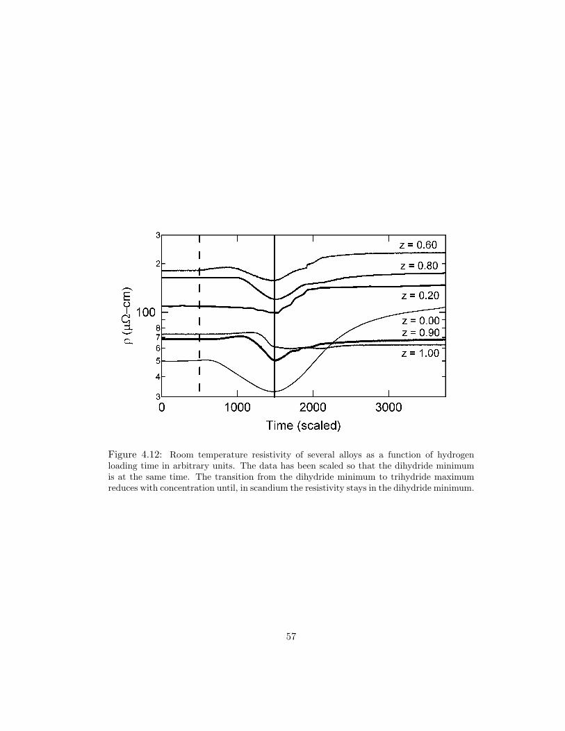
Figure 4.12: Room temperature resistivity of several alloys as a function of hydrogenloading time in arbitrary units. The data has been scaled so that the dihydride minimumis at the same time. The transition from the dihydride minimum to trihydride maximumreduces with concentration until, in scandium the resistivity stays in the dihydride minimum.
57
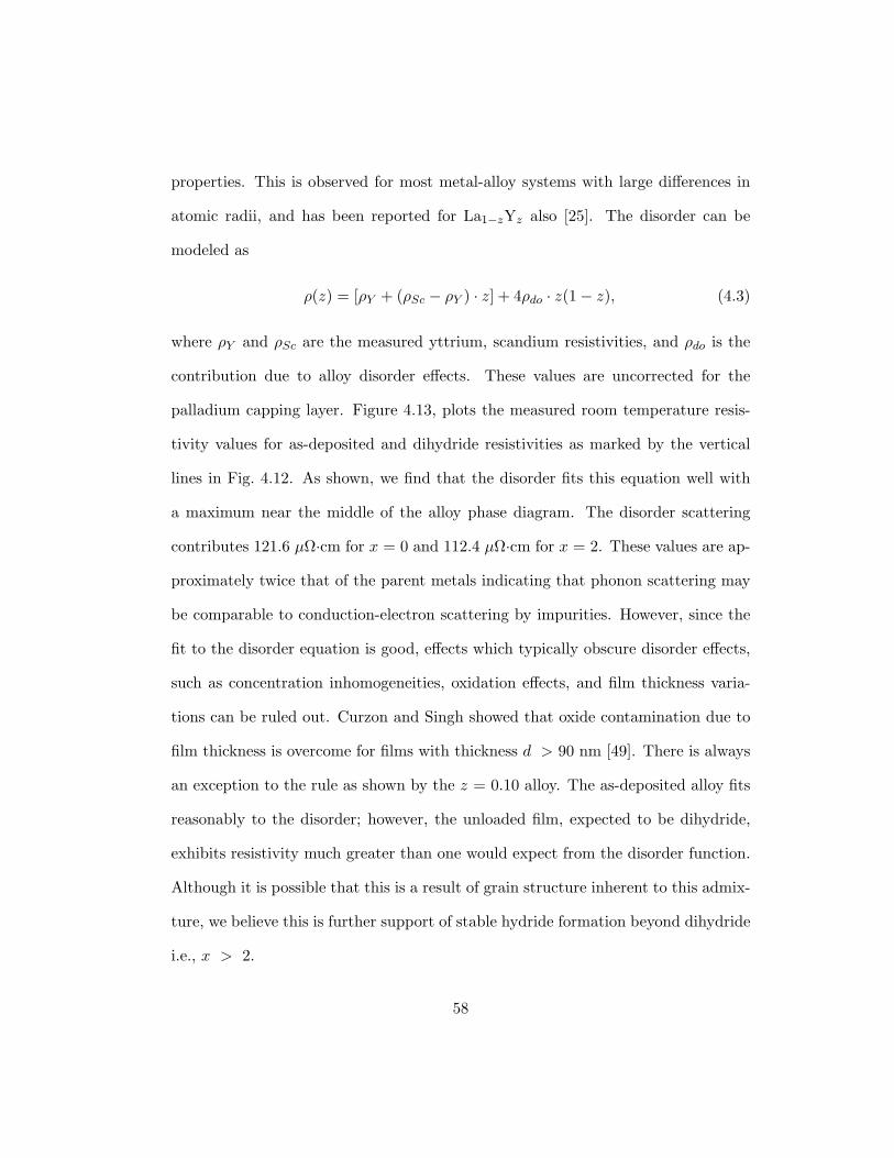
properties. This is observed for most metal-alloy systems with large differences in
atomic radii, and has been reported for La1−zYz also [25]. The disorder can be
modeled as
ρ(z) = [ρY + (ρSc − ρY ) · z] + 4ρdo · z(1 − z), (4.3)
where ρY and ρSc are the measured yttrium, scandium resistivities, and ρdo is the
contribution due to alloy disorder effects. These values are uncorrected for the
palladium capping layer. Figure 4.13, plots the measured room temperature resis-
tivity values for as-deposited and dihydride resistivities as marked by the vertical
lines in Fig. 4.12. As shown, we find that the disorder fits this equation well with
a maximum near the middle of the alloy phase diagram. The disorder scattering
contributes 121.6 µΩ·cm for x = 0 and 112.4 µΩ·cm for x = 2. These values are ap-
proximately twice that of the parent metals indicating that phonon scattering may
be comparable to conduction-electron scattering by impurities. However, since the
fit to the disorder equation is good, effects which typically obscure disorder effects,
such as concentration inhomogeneities, oxidation effects, and film thickness varia-
tions can be ruled out. Curzon and Singh showed that oxide contamination due to
film thickness is overcome for films with thickness d > 90 nm [49]. There is always
an exception to the rule as shown by the z = 0.10 alloy. The as-deposited alloy fits
reasonably to the disorder; however, the unloaded film, expected to be dihydride,
exhibits resistivity much greater than one would expect from the disorder function.
Although it is possible that this is a result of grain structure inherent to this admix-
ture, we believe this is further support of stable hydride formation beyond dihydride
i.e., x > 2.
58
Figure 4.13: Modeling of disorder in room temperature electrical resistivity from Eqn. 4.1.
59
One can determine whether surface effects due to film thickness should be ob-
served. These contributions typically occur for films of thickness on the order of the
electron mean free path, d ≈ λmfp. The electron mean free path is λmfp = vF τ . The
Fermi energies for yttrium and scandium are taken from the band structure models of
Altmann and Bradley [55]. These values are εF (Y) = 4.58 eV and εF (Sc) = 5.98 eV.
Scandium fermi surface calculations have also been reported by Fleming and Loucks
[56] with a value of εF (Sc) = 5.66 eV. Then, the Fermi velocities may be estimated
to be, vF (Y) = 1.3×10⁶ m/s and vF (Sc) = 1.5×10⁶ m/s. From our resistivities,
we estimate τ using the Drude model and obtain τ = m/ne2ρ = 1.6×10⁻¹⁵ s for
yttrium and τ = 9.1×10⁻¹⁶ s for scandium. From these values we compute a mean
free path of λmfp = 2.0 nm in yttrium and λmfp = 1.3 nm in scandium. Therefore,
our films have d λmfp, and surface effects are not expected to have an affect on
resistivity measurements. This is in agreement with findings for the La-Y system
[6].
Finally, because the fit to the disorder model is good, and the mean free
path of electrons is much smaller than the film dimensions, we can conclude that
the alloy resistivities are dominated by impurity scattering with length scales on the
order of several atomic lengths.
4.3.2 Temperature-Dependent Measurements
To get a better understanding of the electrical behavior discussed in the
previous section, we have measured the temperature dependent ac resistivity for
the temperature range 4–295 K. Results for the unloaded, nearly dihydride concen-
60
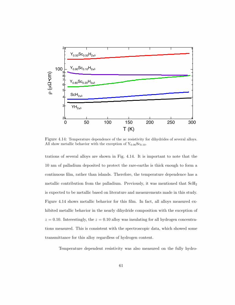
2
3
4
5
6
789
100
2ρ
(µΩ
•cm
)
300250200150100500
T (K)
YH2±δ
ScH2±δ
Y0.80Sc0.20H2±δ
Y0.50Sc0.50H2±δ
Y0.90Sc0.10H2±δ
Figure 4.14: Temperature dependence of the ac resistivity for dihydrides of several alloys.All show metallic behavior with the exception of Y0.90Sc0.10.
trations of several alloys are shown in Fig. 4.14. It is important to note that the
10 nm of palladium deposited to protect the rare-earths is thick enough to form a
continuous film, rather than islands. Therefore, the temperature dependence has a
metallic contribution from the palladium. Previously, it was mentioned that ScH2
is expected to be metallic based on literature and measurements made in this study.
Figure 4.14 shows metallic behavior for this film. In fact, all alloys measured ex-
hibited metallic behavior in the nearly dihydride composition with the exception of
z = 0.10. Interestingly, the z = 0.10 alloy was insulating for all hydrogen concentra-
tions measured. This is consistent with the spectroscopic data, which showed some
transmittance for this alloy regardless of hydrogen content.
Temperature dependent resistivity was also measured on the fully hydro-
61
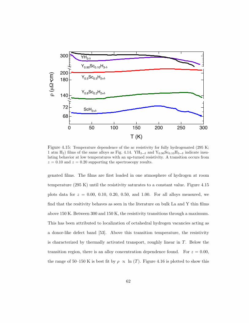
200180
140ρ (µ
Ω•c
m)
300250200150100500
T (K)
72
68
300 YH3-δ
Y0.90Sc0.10H3-δ
Y0.8Sc0.2H2+δ
Y0.5Sc0.5H2+δ
ScH2+δ
Figure 4.15: Temperature dependence of the ac resistivity for fully hydrogenated (295 K;1 atm H2) films of the same alloys as Fig. 4.14. YH3−δ and Y0.90Sc0.10H3−δ indicate insu-lating behavior at low temperatures with an up-turned resistivity. A transition occurs fromz = 0.10 and z = 0.20 supporting the spectroscopy results.
genated films. The films are first loaded in one atmosphere of hydrogen at room
temperature (295 K) until the resistivity saturates to a constant value. Figure 4.15
plots data for z = 0.00, 0.10, 0.20, 0.50, and 1.00. For all alloys measured, we
find that the resitivity behaves as seen in the literature on bulk La and Y thin films
above 150 K. Between 300 and 150 K, the resistivity transitions through a maximum.
This has been attributed to localization of octahedral hydrogen vacancies acting as
a donor-like defect band [53]. Above this transition temperature, the resistivity
is characterized by thermally activated transport, roughly linear in T . Below the
transition region, there is an alloy concentration dependence found. For z = 0.00,
the range of 50–150 K is best fit by ρ ∝ ln (T ). Figure 4.16 is plotted to show this
62
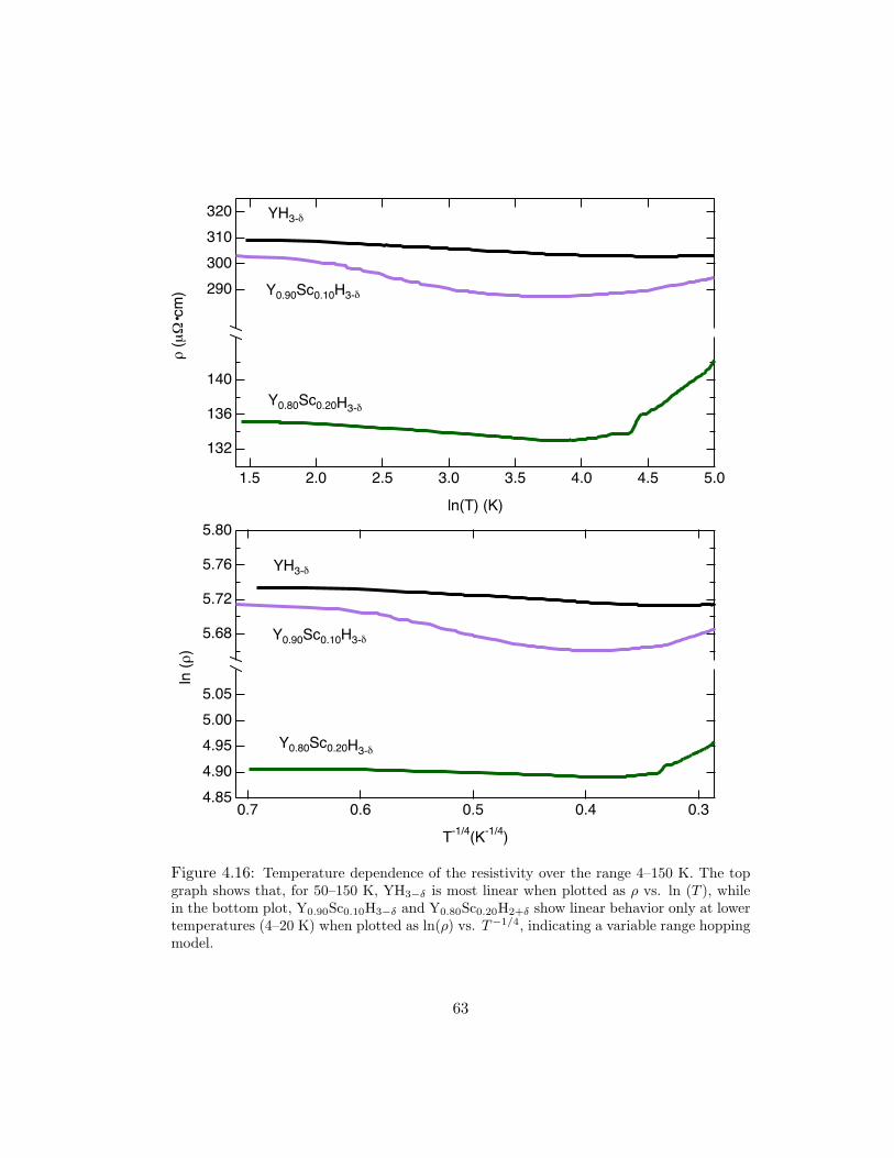
320
310
300
290
5.04.54.03.53.02.52.01.5
ln(T) (K)
140
136
132
ρ (µ
Ω•c
m) Y0.90Sc0.10H3-δ
YH3-δ
Y0.80Sc0.20H3-δ
5.80
5.76
5.72
5.68
0.7 0.6 0.5 0.4 0.3
T-1/4(K-1/4)
5.05
5.00
4.95
4.90
4.85
ln (
ρ)
Y0.90Sc0.10H3-δ
YH3-δ
Y0.80Sc0.20H3-δ
Figure 4.16: Temperature dependence of the resistivity over the range 4–150 K. The topgraph shows that, for 50–150 K, YH3−δ is most linear when plotted as ρ vs. ln (T ), whilein the bottom plot, Y0.90Sc0.10H3−δ and Y0.80Sc0.20H2+δ show linear behavior only at lowertemperatures (4–20 K) when plotted as ln(ρ) vs. T−1/4, indicating a variable range hoppingmodel.
63
linear dependence. This has been observed previously by Huiberts et al. [36]. It
is believed that this is attributable to one of two mechanisms. Kondo scattering is
one possibility. Hydrogen vacancies introduce magnetic moments due to the H− na-
ture of hydrogen in yttrium [23]. These act as scatterers inducing a spin-scattering
resistivity term that depends logarithmically on temperature. The implications of
Kondo scattering are that local magnetic moments appear as one approaches the
metal-insulator transition. Hall effect measurements by Huiberts et al. [36], reveal
a quadratic, negative magnetoresistance consistent with the presence of the Kondo
effect. Another suggestion for the logarithmic temperature dependence is in terms
of 2D weak electron localization. In this model, the film is stratified into layers of
conducting YH2 and insulating YH3. The spacing between layers is comparable to
the c-axis lattice spacing. Since the slope of the logarithmic dependence will depend
on spin scattering and disorder effects of electron interactions, the observed behavior
would not be inconsistent with 2D localization. In the reference by Huiberts, one
can extract the trihydride deficiency from,
R(50K) =788δ
(0.32 − 2.1δ). (4.4)
In this equation, R = ρ/d, where d is the film thickness. The choice of 50 K comes
from the minimum temperature of the logarithmic dependence. We find δ = 0.15,
which is reasonable for the observed behavior.
The z = 0.10 and 0.20 alloys are poorly fit by the ρ ∝ ln(T ) over the 50–
150 K range; however, at lower temperatures (4–20 K), all measured alloys can be fit
to ln(ρ) ∝ T−1/4. This is indicative of variable range hopping (VRH) seen in many
64
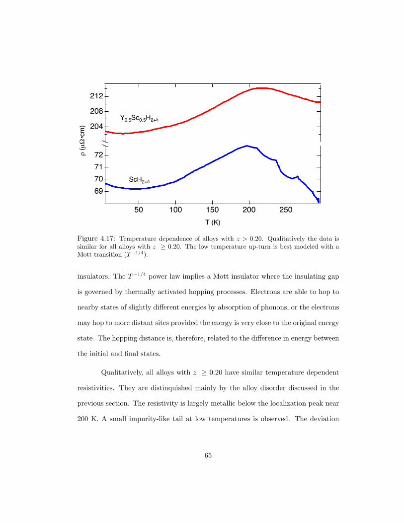
72
71
70
69
ρ (µ
Ω•c
m)
25020015010050
T (K)
212
208
204
ScH2+δ
Y0.5Sc0.5H2+δ
Figure 4.17: Temperature dependence of alloys with z > 0.20. Qualitatively the data issimilar for all alloys with z ≥ 0.20. The low temperature up-turn is best modeled with aMott transition (T−1/4).
insulators. The T−1/4 power law implies a Mott insulator where the insulating gap
is governed by thermally activated hopping processes. Electrons are able to hop to
nearby states of slightly different energies by absorption of phonons, or the electrons
may hop to more distant sites provided the energy is very close to the original energy
state. The hopping distance is, therefore, related to the difference in energy between
the initial and final states.
Qualitatively, all alloys with z ≥ 0.20 have similar temperature dependent
resistivities. They are distinquished mainly by the alloy disorder discussed in the
previous section. The resistivity is largely metallic below the localization peak near
200 K. A small impurity-like tail at low temperatures is observed. The deviation
65
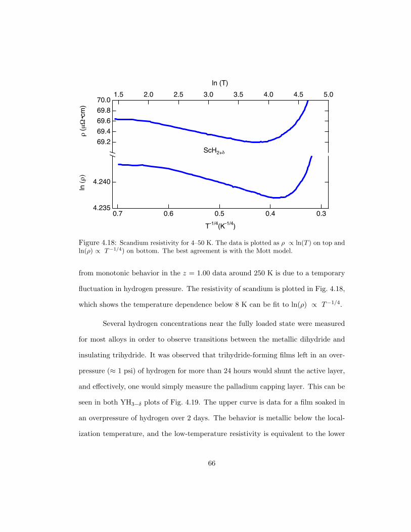
4.240
4.235
ln (
ρ)
0.7 0.6 0.5 0.4 0.3
T-1/4(K-1/4)
70.0
69.8
69.6
69.4
69.2
ρ (µ
Ω•c
m)
5.04.54.03.53.02.52.01.5
ln (T)
ScH2+δ
Figure 4.18: Scandium resistivity for 4–50 K. The data is plotted as ρ ∝ ln(T ) on top andln(ρ) ∝ T−1/4) on bottom. The best agreement is with the Mott model.
from monotonic behavior in the z = 1.00 data around 250 K is due to a temporary
fluctuation in hydrogen pressure. The resistivity of scandium is plotted in Fig. 4.18,
which shows the temperature dependence below 8 K can be fit to ln(ρ) ∝ T−1/4.
Several hydrogen concentrations near the fully loaded state were measured
for most alloys in order to observe transitions between the metallic dihydride and
insulating trihydride. It was observed that trihydride-forming films left in an over-
pressure (≈ 1 psi) of hydrogen for more than 24 hours would shunt the active layer,
and effectively, one would simply measure the palladium capping layer. This can be
seen in both YH3−δ plots of Fig. 4.19. The upper curve is data for a film soaked in
an overpressure of hydrogen over 2 days. The behavior is metallic below the local-
ization temperature, and the low-temperature resistivity is equivalent to the lower
66
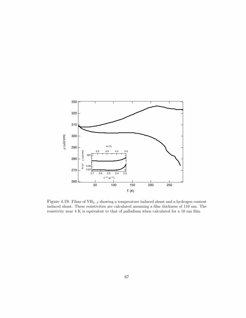
330
320
310
300
290
280
270
260
ρ (µ
Ω•c
m)
25020015010050
T (K)
5.06
5.04ln (
ρ)
0.7 0.6 0.5 0.4 0.3
T-1/4 (K-1/4)
325
ρ (µ
Ω•c
m) 5.04.03.02.0
ln (T)
Figure 4.19: Films of YH3−δ showing a temperature induced shunt and a hydrogen contentinduced shunt. These resistivities are calculated assuming a film thickness of 110 nm. Theresistivity near 4 K is equivalent to that of palladium when calculated for a 10 nm film.
67
curve, where the yttrium resistance becomes so large at low temperatures that the
resistivity saturates at a value that is, for a 10 nm Pd film, consistent with measured
palladium resistivities (ρPdHx ≈ 29 µΩ·cm). The inset is the same data as the upper
curve plotted to show that for the metallic behavior of palladium, neither insulat-
ing scheme discussed above (ln(T ) or T−1/4) addresses the temperature dependence
appropriately. Similar behavior was observed in the z = 0.10 alloys.
4.4 Discussion
The loss of octahedral site occupancy as a function of Sc concentration in
Y1−zSczHx causes the suppression of the optical switching properties seen in metal
trihydrides. Substitution of Sc for Y indicates that there is a minimum cell vol-
ume for trihydride forming rare-earth metals around 177 A3. For an hcp (or fcc)
structure, the combinatorics can be easily calculated to determine the fraction of
hydrogen that have a specific number of nearest neighbor scandium atoms. For
our samples, we have a lattice with N octahedral sites each having X = 6 nearest-
neighbor lattice sites. For a homogeneous alloy, where the atomic distribution is
essentially random, the fraction of octahedrals, Nn/N , with X − n yttrium and n
scandium nearest neighbors is
Nn
N=
X!(X − n)!n!
(1 − z)X−nzn, (4.5)
where z is the scandium concentration as it has been denoted previously. Figure 4.20
plots Nn/N for scandium concentrations 0.00 ≤ z ≤ 1.00, in increments of 0.05.
The first thing that jumps out is the sharp drop of the fraction of octahedral sites
with n = 0 nearest neighbor scandiums. In addition, the fraction with n = 1 becomes
68
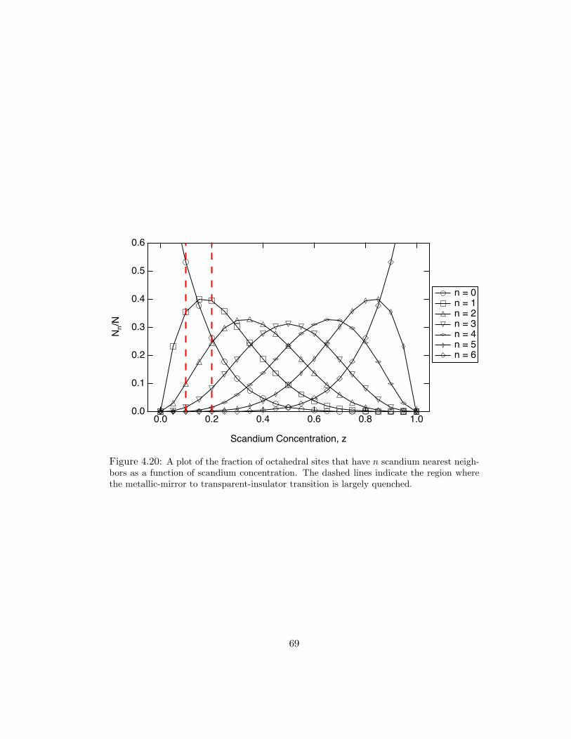
0.6
0.5
0.4
0.3
0.2
0.1
0.0
Nn/
N
1.00.80.60.40.20.0
Scandium Concentration, z
n = 0 n = 1 n = 2 n = 3 n = 4 n = 5 n = 6
Figure 4.20: A plot of the fraction of octahedral sites that have n scandium nearest neigh-bors as a function of scandium concentration. The dashed lines indicate the region wherethe metallic-mirror to transparent-insulator transition is largely quenched.
69
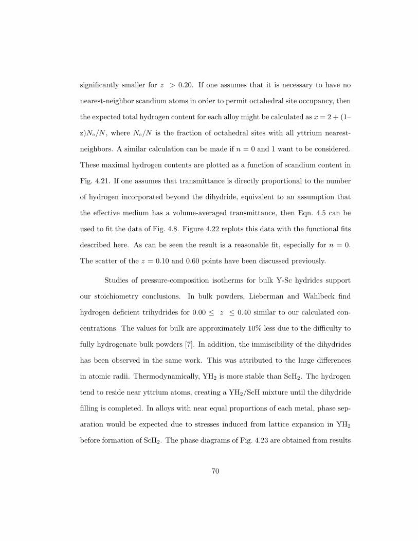
significantly smaller for z > 0.20. If one assumes that it is necessary to have no
nearest-neighbor scandium atoms in order to permit octahedral site occupancy, then
the expected total hydrogen content for each alloy might be calculated as x = 2 + (1–
z)N/N , where N/N is the fraction of octahedral sites with all yttrium nearest-
neighbors. A similar calculation can be made if n = 0 and 1 want to be considered.
These maximal hydrogen contents are plotted as a function of scandium content in
Fig. 4.21. If one assumes that transmittance is directly proportional to the number
of hydrogen incorporated beyond the dihydride, equivalent to an assumption that
the effective medium has a volume-averaged transmittance, then Eqn. 4.5 can be
used to fit the data of Fig. 4.8. Figure 4.22 replots this data with the functional fits
described here. As can be seen the result is a reasonable fit, especially for n = 0.
The scatter of the z = 0.10 and 0.60 points have been discussed previously.
Studies of pressure-composition isotherms for bulk Y-Sc hydrides support
our stoichiometry conclusions. In bulk powders, Lieberman and Wahlbeck find
hydrogen deficient trihydrides for 0.00 ≤ z ≤ 0.40 similar to our calculated con-
centrations. The values for bulk are approximately 10% less due to the difficulty to
fully hydrogenate bulk powders [7]. In addition, the immiscibility of the dihydrides
has been observed in the same work. This was attributed to the large differences
in atomic radii. Thermodynamically, YH2 is more stable than ScH2. The hydrogen
tend to reside near yttrium atoms, creating a YH2/ScH mixture until the dihydride
filling is completed. In alloys with near equal proportions of each metal, phase sep-
aration would be expected due to stresses induced from lattice expansion in YH2
before formation of ScH2. The phase diagrams of Fig. 4.23 are obtained from results
70
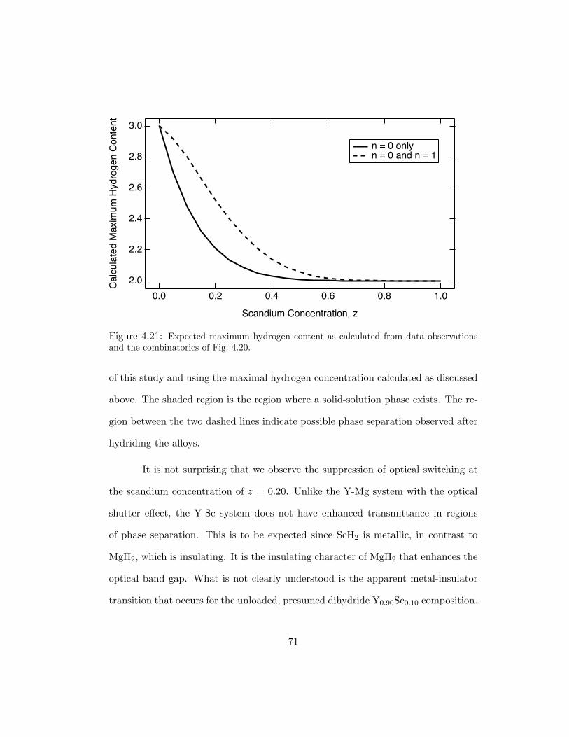
3.0
2.8
2.6
2.4
2.2
2.0Cal
cula
ted
Max
imum
Hyd
roge
n C
onte
nt
1.00.80.60.40.20.0
Scandium Concentration, z
n = 0 only n = 0 and n = 1
Figure 4.21: Expected maximum hydrogen content as calculated from data observationsand the combinatorics of Fig. 4.20.
of this study and using the maximal hydrogen concentration calculated as discussed
above. The shaded region is the region where a solid-solution phase exists. The re-
gion between the two dashed lines indicate possible phase separation observed after
hydriding the alloys.
It is not surprising that we observe the suppression of optical switching at
the scandium concentration of z = 0.20. Unlike the Y-Mg system with the optical
shutter effect, the Y-Sc system does not have enhanced transmittance in regions
of phase separation. This is to be expected since ScH2 is metallic, in contrast to
MgH2, which is insulating. It is the insulating character of MgH2 that enhances the
optical band gap. What is not clearly understood is the apparent metal-insulator
transition that occurs for the unloaded, presumed dihydride Y0.90Sc0.10 composition.
71
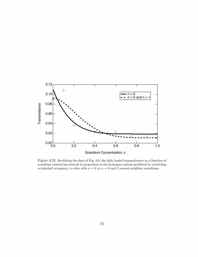
0.12
0.10
0.08
0.06
0.04
0.02
0.00
Tra
nsm
ittan
ce
1.00.80.60.40.20.0
Scandium Concentration, z
n = 0 n = 0 and n = 1
Figure 4.22: Revisiting the data of Fig. 4.8, the fully loaded transmittance as a function ofscandium content has been fit in proportion to the hydrogen content predicted by restrictingoctahedral occupancy to sites with n = 0 or n = 0 and 1 nearest-neighbor scandiums.
72
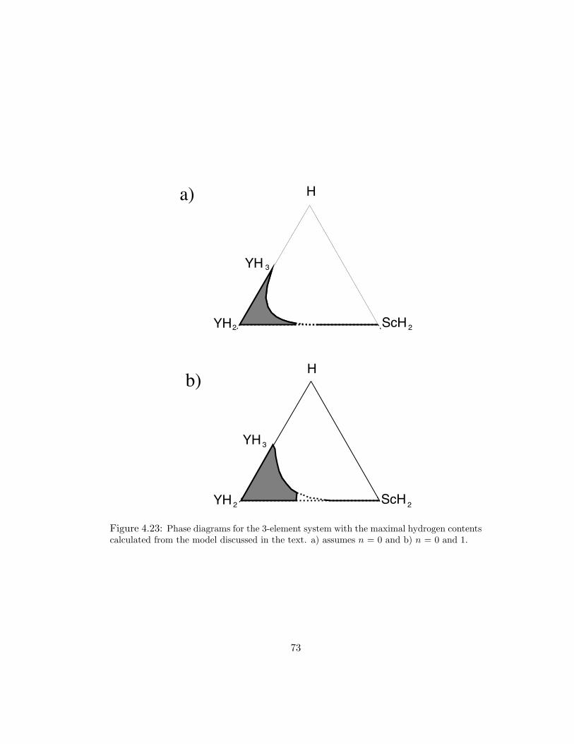
H
YH2
YH 3
ScH 2
a)
b)
YH 2
H
YH 3
ScH 2
Figure 4.23: Phase diagrams for the 3-element system with the maximal hydrogen contentscalculated from the model discussed in the text. a) assumes n = 0 and b) n = 0 and 1.
73
It may be that this composition forms a trihydride phase that is more stable than
other alloy compositions studied. This is in accord with our lack of observation of
a dihydride transmittance peak. The possibility of an unusually stable trihydride
phase may be useful for applications such as pixel-switching in flat-panel displays,
where remaining closer to the phase transition might reduce switching speeds, which
are currently an order of magnitude too large.
74
Chapter 5
Summary and Future Investigations
“That rug really tied the room together... did it not?... did it not?
- Walter in The Big Lebowski
The change in optical properties of the Y1−zSczHx system is due to reduction
of the unit cell volume of approximately 30%. Up to the dihydride phase, hydrogen
in yttrium primarily fills the tetrahedral sites. Typically up to x = 2, only a few
atomic percent of hydrogen occupy octahedral sites, which have higher mobility than
tetrahedral sites [15]. Because the transition occurs beyond the dihydride phase,
when octahedral sites become significantly occupied, it is assumed that this filling
is responsible for the optical transition. Therefore, in the yttrium-scandium alloys,
the quenching of the optical transmittance is most likely due to the loss of available
octahedral sites caused by the reduction of lattice dimensions. In the Y1−zSczHx we
have studied, the optical and metal to insulator transitions are largely suppressed
for scandium concentrations above z = 0.20. It is interesting to note that the unit
cell volume we measure for Y0.80Sc0.20 (176.63 A3) is equal to the unit cell volume
of lutetium (VLu = 176.64 A3), the largest known rare-earth element that does not
form a trihydride. This suggests that studies on the Y1−zLuzHx alloy system would
be very interesting, and the lutetium 5d16s2 electronic structure make it simple
75
to correlate results to these studies. We have also identified a metal to insulator
transition between Y and Y0.90Sc0.10, apparently in the middle of the the transition
from an optically switchable material to a non-switchable material.
From statistical modeling it was found that z = 0.20 is not an unexpected
concentration beyond which to observe the optical switching to be quenched. Fur-
ther study of the alloy phase diagram for the transition region 0.00 < z < 0.20
is underway. It is important that the phase separation be better identified. Two
possible directions for this study have been planned. The first is to use substrate
heating, which will increase the crystallinity of the films. This would provide better
XRD for analysis. Another regime for the study of phase separation is to investi-
gate epitaxial films. Epitaxial materials provide an extremely simple way to identify
phase separation, as well as additional effects, for example, epitaxial strain from a
substrate or buffer-layer. Design, construction, and installation of the equipment to
enable these two capabilities have been initiated by the author. In addition, x-ray
diffraction capabilities for fully hydrided films should also be developed along with
electrochemistry for hydrogen loading. Electrochemical loading enables the deter-
mination of hydrogen concentration. Finally, modifications of an AFM and/or STM
head to permit topographical and spectroscopic studies during hydrogen loading
would provide complementary microscopic information.
76

Appendices
77
Appendix A
Vacuum and Film Deposition
Much of the following material was written in my Master’s thesis, however, at
that time I still had not grown a single film [74]. I have since had much experience
with the chamber. This is an updated user’s guide to growing thin films using
e-beam evaporation. I will avoid discussions of the evaporators, power supplies,
pumps, substrate stage, and leak detection because I feel my past thesis is adequate
for these topics.
A.1 Growing a Film
The vacuum chamber is designed such that it is able to sustain vacuum
pressures of 10−10 torr or better. However, to date, ultimate pressures on the order
of 10−8 have been achieved. The current mode of operation is to break vacuum
about once a week to change evaporant material for a new set of films. This is
partly why the chamber pressure is not optimal. There is also likely a leak in this
range that should be sealed. The metal-hydrides did not require lower pressures,
and I therefore forewent further leak detection.
Since my Master’s thesis, we have a purchased a new dry pumping station
which requires only a flick of a switch (once the chamber is sealed). The station will
bring the chamber to ≈ 10−5 torr within one hour and 10−7 torr overnight. At 10−5
78
torr, the ion gauge can be turned on (making sure it is on the lowest, 10−4, scale).
When the chamber reaches 10−6 torr, the ion pump should be turned on in “start”
mode until the chamber reaches 10−7 torr. I generally leave it in “start” mode
because the beginning of evaporations can create lots of vapor pressure, and it gets
frustrating to turn the ion pump on over and over. I have always left the valve open
so that both the turbo pump and ion pump are actively pumping the chamber at
all times. The pressure during evaporation will rise too much if both pumps are not
active. Once the chamber is in the 10−7 torr range, gettering due to the evaporation
will reduce the pressure to 10−8 torr. To achieve this, simply turn on the evaporator
filaments to 14 amps. This should be done slowly, as long as several hours, such
that the pressure doesn’t get above 10−6 torr. When the current is 14 amps, turn on
the voltage to the first evaporant. Slowly increase the voltage keeping the pressure
as low as possible. Typically, 300–700 V is enough. As a rule of thumb, I switch to
the emission current setting rather than the accelerating voltage. If the evaporant
is properly located within a couple of millimeters of the filament loop, the emission
current will rise to the first mark (10 mA). This is enough emission current and
voltage to cause evaporation. It may take some tweaking of the evaporant position
with respect to the filament. If this amount of emission current is not obtained
with less than 1000 V, something is wrong. When the metal is heated sufficiently,
it will begin to reduce the chamber pressure. Wait until the pressure has dropped
to 10−8 torr and the growth monitor is measuring 0.1–0.8 A/sec before moving the
substrates into the beam. A growth rate of more than 0.8 A/sec will melt the
evaporant. The growth rate should be kept as constant as possible by feeding the
79
evaporant toward the filament and adjusting the voltage/emission current.
A.2 Some Suggested Modifications
Hopefully, the reader realizes that film crystallization is very low for room
temperature substrate growth. This has a few adverse effects on material charac-
terization. It is therefore recommended that the vacuum chamber be rearranged to
allow for substrate heating. As mentioned in my Master’s thesis, there is a machined
substrate holder and heater spool for this purpose. However, the e-beam evaporators
need to be moved to the port 90 from where they are currently mounted without
the 14” extension tube. This would put them directly across from the 6” view-
port, which has the advantage of seeing the evaporators. There were many failed
attempts to incorporate mirrors in the current configuration. In order to make this
change, the growth monitors will require re-routing. The top flange has already
been adapted with rotary, push/pull, thermocouple, and heater feedthroughs. By
rearranging in this manner, one is able to maintain the highest growth rates of 0.3–
0.8 A/sec and the growth monitors stay close to the substrate for more accurate
film thickness measurement. Finally, substrate shuttering is optimized with the use
of the rotary feedthrough.
80
Appendix B
LabVIEW VIs
Historically, the Markert lab has included Appendices about LabVIEW VIs
which run experiments applicable to the dissertation. It seems that many have
simply inserted the images of the front panel and the diagrams of the wiring with-
out any explanation. These are easily viewed by simply opening the VI. So, why
were they included? Maybe their dissertation needed a few more pages in length.
Maybe it is simply to baffle new students who have never before seen LabVIEW.
So, hopefully, this Appendix will be not only a review of the metal-hydride VIs, but
a decent primer on LabVIEW programming. First, I should state that the acronym
VI stands for virtual instrument. For simplicity, I will continue to use VI.
B.1 Room Temperature VI
The first of two VIs used is the room temperature measurement application,
Metal Hydride TxR.vi. This was designed to measure resistance and transmittance
simultaneously while loading hydrogen into the sample. Originally, resistance would
be read directly from the Linear Research ac resistance bridge (LR-400). For some
unidentified reason, the IEEE interface was causing an older Macintosh to freeze-up.
Before switching to a newer computer, we abandoned reading the LR-400 directly,
and set up the program to read two Keithley 195(A) DMMs set to GPIB addresses
81
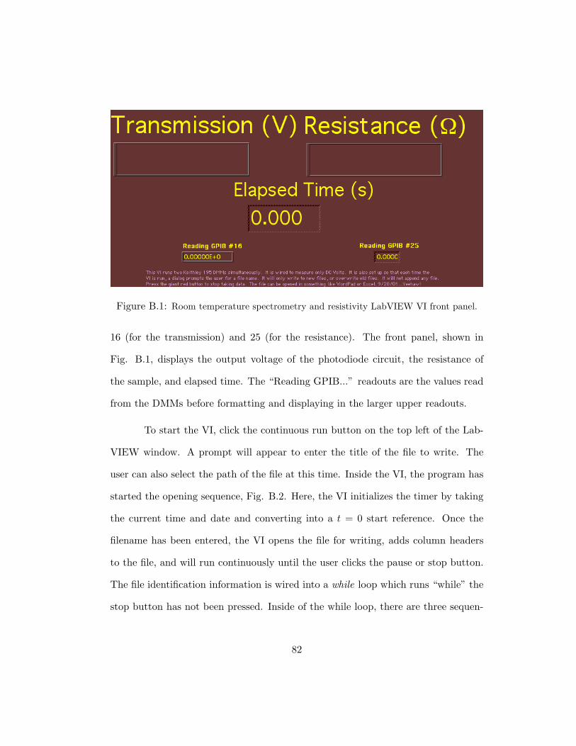
Figure B.1: Room temperature spectrometry and resistivity LabVIEW VI front panel.
16 (for the transmission) and 25 (for the resistance). The front panel, shown in
Fig. B.1, displays the output voltage of the photodiode circuit, the resistance of
the sample, and elapsed time. The “Reading GPIB...” readouts are the values read
from the DMMs before formatting and displaying in the larger upper readouts.
To start the VI, click the continuous run button on the top left of the Lab-
VIEW window. A prompt will appear to enter the title of the file to write. The
user can also select the path of the file at this time. Inside the VI, the program has
started the opening sequence, Fig. B.2. Here, the VI initializes the timer by taking
the current time and date and converting into a t = 0 start reference. Once the
filename has been entered, the VI opens the file for writing, adds column headers
to the file, and will run continuously until the user clicks the pause or stop button.
The file identification information is wired into a while loop which runs “while” the
stop button has not been pressed. Inside of the while loop, there are three sequen-
82
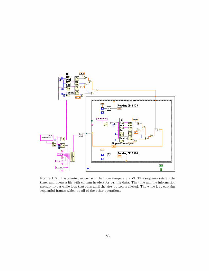
Figure B.2: The opening sequence of the room temperature VI. This sequence sets up thetimer and opens a file with column headers for writing data. The time and file informationare sent into a while loop that runs until the stop button is clicked. The while loop containssequential frames which do all of the other operations.
83
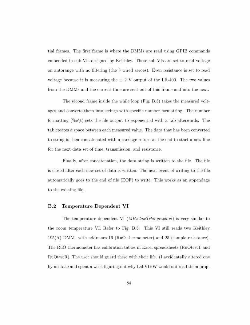
tial frames. The first frame is where the DMMs are read using GPIB commands
embedded in sub-VIs designed by Keithley. These sub-VIs are set to read voltage
on autorange with no filtering (the 3 wired zeroes). Even resistance is set to read
voltage because it is measuring the ± 2 V output of the LR-400. The two values
from the DMMs and the current time are sent out of this frame and into the next.
The second frame inside the while loop (Fig. B.3) takes the measured volt-
ages and converts them into strings with specific number formatting. The number
formatting (%e\t) sets the file output to exponential with a tab afterwards. The
tab creates a space between each measured value. The data that has been converted
to string is then concatenated with a carriage return at the end to start a new line
for the next data set of time, transmission, and resistance.
Finally, after concatenation, the data string is written to the file. The file
is closed after each new set of data is written. The next event of writing to the file
automatically goes to the end of file (EOF) to write. This works as an appendage
to the existing file.
B.2 Temperature Dependent VI
The temperature dependent VI (MHx-lowTrho-graph.vi) is very similar to
the room temperature VI. Refer to Fig. B.5. This VI still reads two Keithley
195(A) DMMs with addresses 16 (RuO thermometer) and 25 (sample resistance).
The RuO thermometer has calibration tables in Excel spreadsheets (RuOtestT and
RuOtestR). The user should guard these with their life. (I accidentally altered one
by mistake and spent a week figuring out why LabVIEW would not read them prop-
84
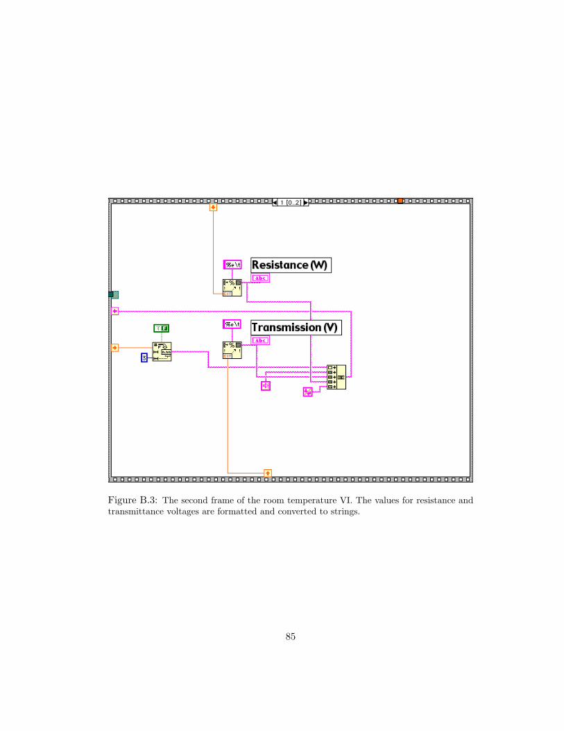
Figure B.3: The second frame of the room temperature VI. The values for resistance andtransmittance voltages are formatted and converted to strings.
85
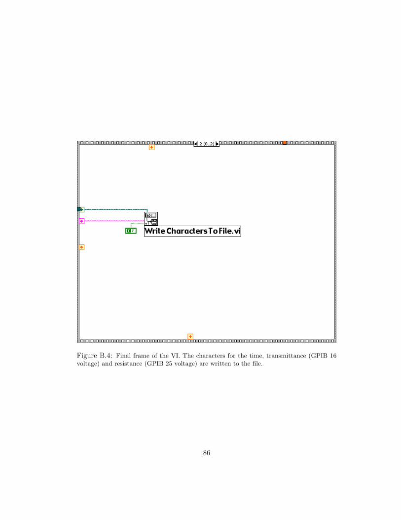
Figure B.4: Final frame of the VI. The characters for the time, transmittance (GPIB 16voltage) and resistance (GPIB 25 voltage) are written to the file.
86
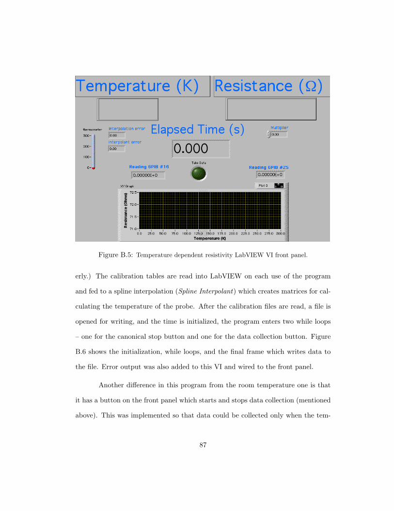
Figure B.5: Temperature dependent resistivity LabVIEW VI front panel.
erly.) The calibration tables are read into LabVIEW on each use of the program
and fed to a spline interpolation (Spline Interpolant) which creates matrices for cal-
culating the temperature of the probe. After the calibration files are read, a file is
opened for writing, and the time is initialized, the program enters two while loops
– one for the canonical stop button and one for the data collection button. Figure
B.6 shows the initialization, while loops, and the final frame which writes data to
the file. Error output was also added to this VI and wired to the front panel.
Another difference in this program from the room temperature one is that
it has a button on the front panel which starts and stops data collection (mentioned
above). This was implemented so that data could be collected only when the tem-
87
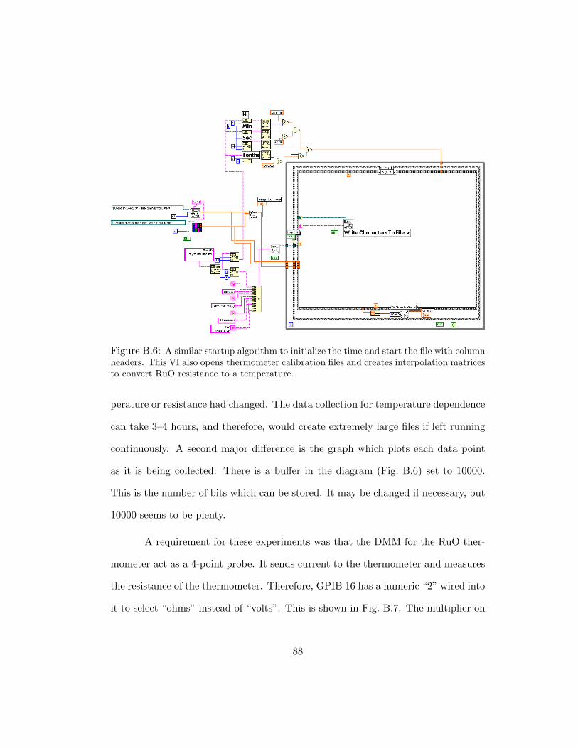
Figure B.6: A similar startup algorithm to initialize the time and start the file with columnheaders. This VI also opens thermometer calibration files and creates interpolation matricesto convert RuO resistance to a temperature.
perature or resistance had changed. The data collection for temperature dependence
can take 3–4 hours, and therefore, would create extremely large files if left running
continuously. A second major difference is the graph which plots each data point
as it is being collected. There is a buffer in the diagram (Fig. B.6) set to 10000.
This is the number of bits which can be stored. It may be changed if necessary, but
10000 seems to be plenty.
A requirement for these experiments was that the DMM for the RuO ther-
mometer act as a 4-point probe. It sends current to the thermometer and measures
the resistance of the thermometer. Therefore, GPIB 16 has a numeric “2” wired into
it to select “ohms” instead of “volts”. This is shown in Fig. B.7. The multiplier on
88
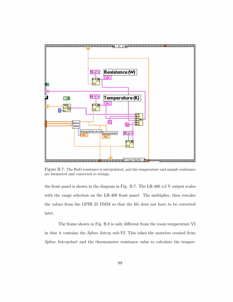
Figure B.7: The RuO resistance is interpolated, and the temperature and sample resistanceare formatted and converted to strings.
the front panel is shown in the diagram in Fig. B.7. The LR-400 ±2 V output scales
with the range selection on the LR-400 front panel. The multiplier, then rescales
the values from the GPIB 25 DMM so that the file does not have to be corrected
later.
The frame shown in Fig. B.8 is only different from the room temperature VI
in that it contains the Spline Interp sub-VI. This takes the matrices created from
Spline Interpolant and the thermometer resistance value to calculate the temper-
89
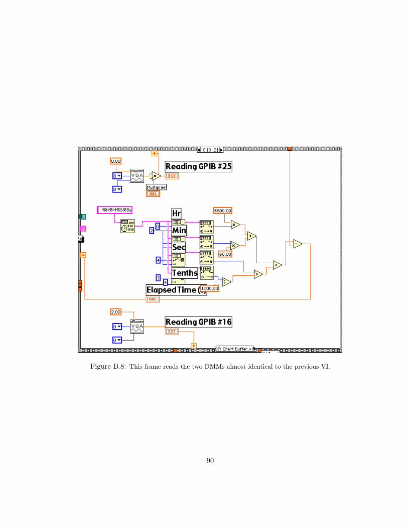
Figure B.8: This frame reads the two DMMs almost identical to the previous VI.
90
ature, which is then sent to the front panel and to the file along with the time,
sample resistance, and actual thermometer resistance. The thermometer resistance
is written to the file in the event that the interpolation goes wrong.
These VIs are about as simple as they can be written. If something should go
wrong with them, hopefully, the information and images here can help reconstruct
them or even better programs. It was originally my intent to make the temperature
dependent VI be automated such that it would take data on its own. This was done
in Boem-Hoan O’s old version by checking the temperature and sample resistance
and taking a data point if a significant change in either had occured. In any event,
good luck, we are all counting on you.
91
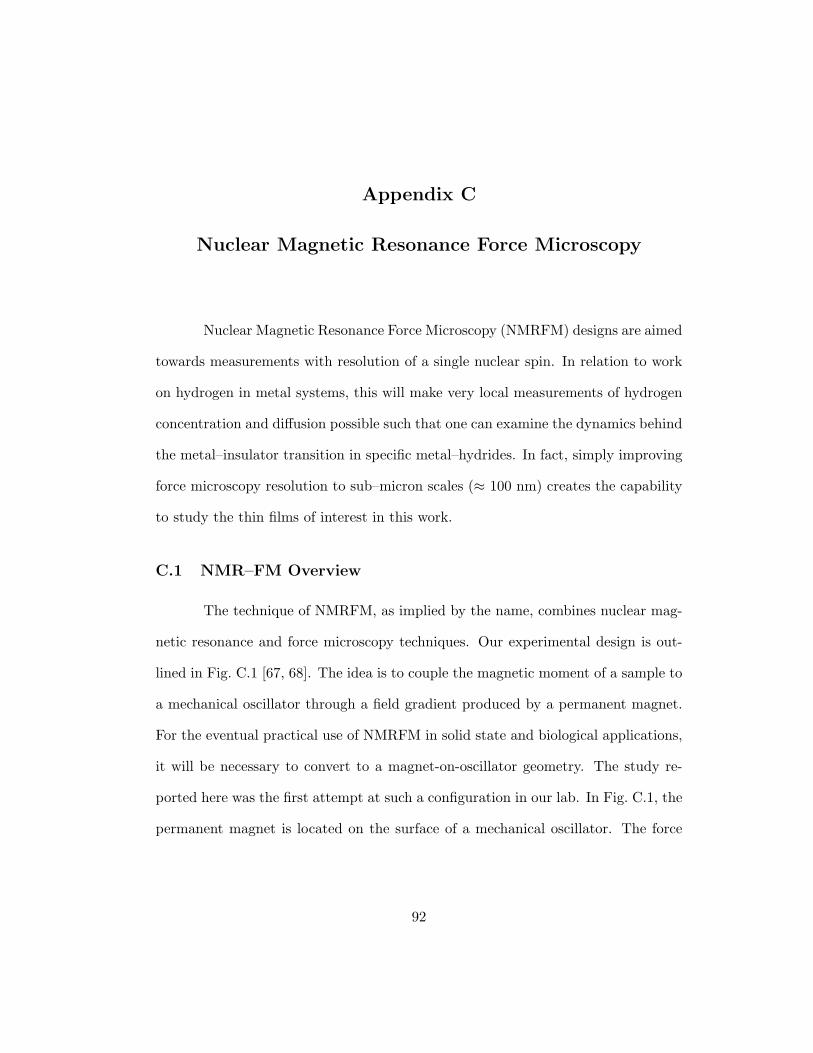
Appendix C
Nuclear Magnetic Resonance Force Microscopy
Nuclear Magnetic Resonance Force Microscopy (NMRFM) designs are aimed
towards measurements with resolution of a single nuclear spin. In relation to work
on hydrogen in metal systems, this will make very local measurements of hydrogen
concentration and diffusion possible such that one can examine the dynamics behind
the metal–insulator transition in specific metal–hydrides. In fact, simply improving
force microscopy resolution to sub–micron scales (≈ 100 nm) creates the capability
to study the thin films of interest in this work.
C.1 NMR–FM Overview
The technique of NMRFM, as implied by the name, combines nuclear mag-
netic resonance and force microscopy techniques. Our experimental design is out-
lined in Fig. C.1 [67, 68]. The idea is to couple the magnetic moment of a sample to
a mechanical oscillator through a field gradient produced by a permanent magnet.
For the eventual practical use of NMRFM in solid state and biological applications,
it will be necessary to convert to a magnet-on-oscillator geometry. The study re-
ported here was the first attempt at such a configuration in our lab. In Fig. C.1, the
permanent magnet is located on the surface of a mechanical oscillator. The force
92
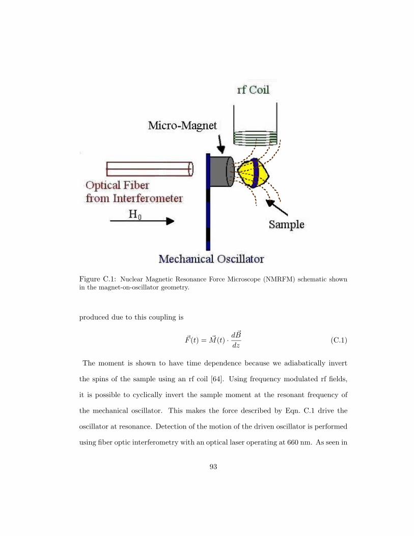
Figure C.1: Nuclear Magnetic Resonance Force Microscope (NMRFM) schematic shownin the magnet-on-oscillator geometry.
produced due to this coupling is
F (t) = M(t) · d B
dz(C.1)
The moment is shown to have time dependence because we adiabatically invert
the spins of the sample using an rf coil [64]. Using frequency modulated rf fields,
it is possible to cyclically invert the sample moment at the resonant frequency of
the mechanical oscillator. This makes the force described by Eqn. C.1 drive the
oscillator at resonance. Detection of the motion of the driven oscillator is performed
using fiber optic interferometry with an optical laser operating at 660 nm. As seen in
93
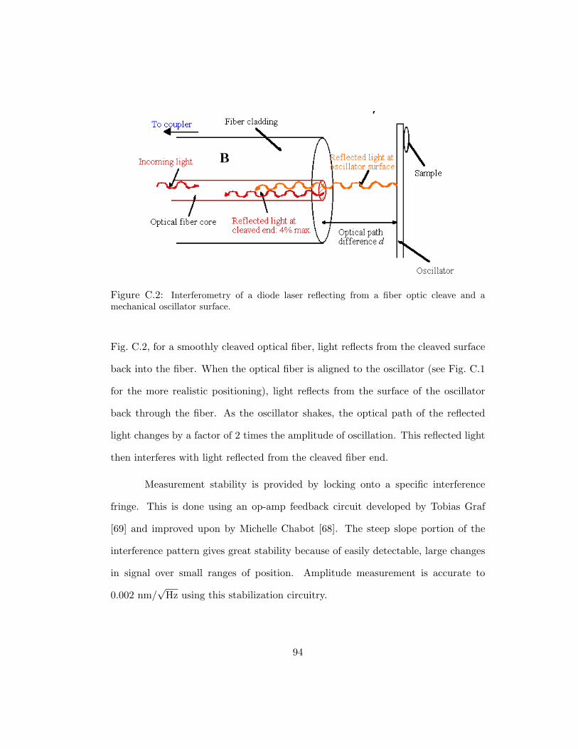
Figure C.2: Interferometry of a diode laser reflecting from a fiber optic cleave and amechanical oscillator surface.
Fig. C.2, for a smoothly cleaved optical fiber, light reflects from the cleaved surface
back into the fiber. When the optical fiber is aligned to the oscillator (see Fig. C.1
for the more realistic positioning), light reflects from the surface of the oscillator
back through the fiber. As the oscillator shakes, the optical path of the reflected
light changes by a factor of 2 times the amplitude of oscillation. This reflected light
then interferes with light reflected from the cleaved fiber end.
Measurement stability is provided by locking onto a specific interference
fringe. This is done using an op-amp feedback circuit developed by Tobias Graf
[69] and improved upon by Michelle Chabot [68]. The steep slope portion of the
interference pattern gives great stability because of easily detectable, large changes
in signal over small ranges of position. Amplitude measurement is accurate to
0.002 nm/√
Hz using this stabilization circuitry.
94
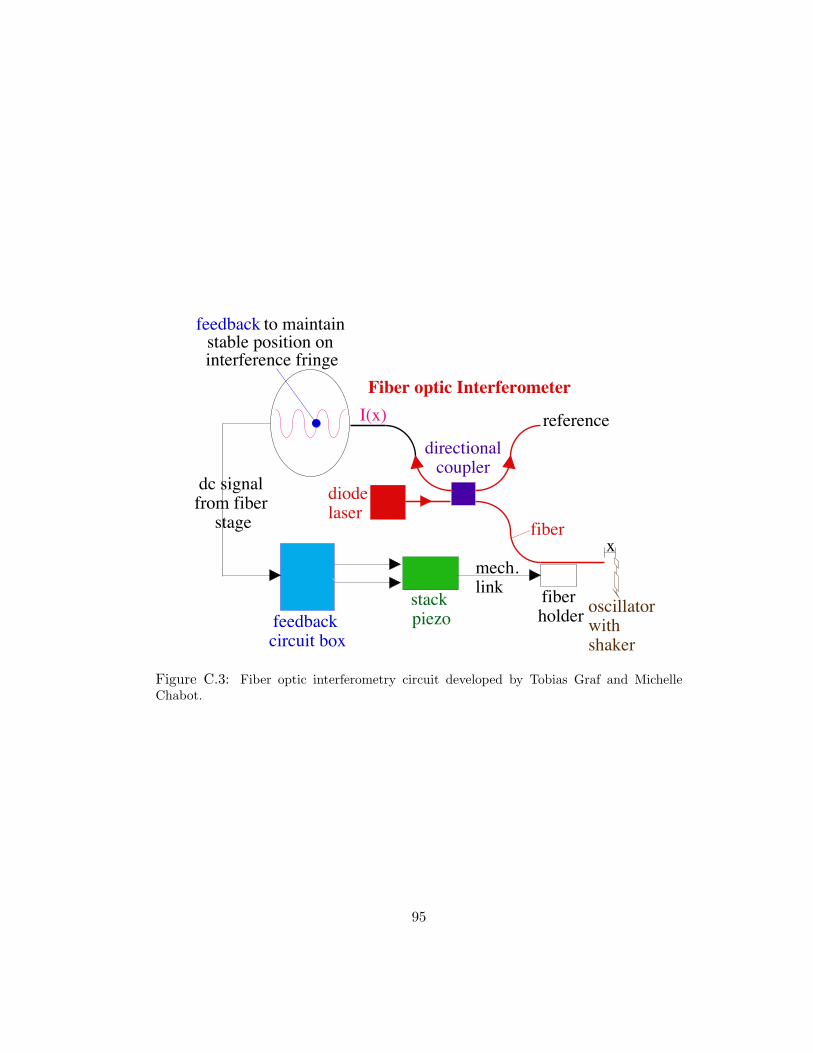
oscillator with shaker
reference
directionalcoupler
diode laser
fiber
feedback circuit box
stack piezo
mech. link
Fiber optic Interferometer
I(x)
feedback to maintain stable position on interference fringe
fiber holder
x
dc signal from fiber
stage
Figure C.3: Fiber optic interferometry circuit developed by Tobias Graf and MichelleChabot.
95
As derived by Nyquist, the minimum force which can be measured is
Fmin(N√Hz
) =
√4kBTkosc
Qω(C.2)
Therefore, the sensitivity of this type of force detection relies solely on the thermo-
dynamic and mechanical properties of the oscillators used [63]. Looking at Eqn. C.1
and C.2, one can see that there are several considerations to be made. One, which
is extremely important, is that of the field gradient in Eqn. C.1. However, there
exists a trade–off between the field gradient magnitude and number of contributing
spins which will lie within a “resonant slice” of appropriate field gradient. If the
field gradient becomes too small, the force created may not be large enough to be
measured above thermal noise of the oscillator. When the field gradient becomes too
large, the resonant slice becomes thin, reducing the number of contributing spins.
In this case, M(t) becomes small, and again, the force is too small to be detected.
Since the metal-hydride films are on the order of 0.1 µm thick and have a
surface area of 1cm×1cm, One obtains a necessary field gradient of
dB
dz≈ 10G
0.1µm= 100
G
µm(C.3)
resulting from the use of a pulsed rf field of 10 Gauss. Eventually, it will be interest-
ing to increase this field gradient to see the hydrogen behavior on an atomic scale.
However, even observation of hydrogen behavior within the entire film is a vast im-
provement to bulk interstitial hydrogen studies. For this purpose, characterization
studies have been made of micron sized magnets on oscillators.
The magnitude of the field gradient is directly related to the aspect ra-
tio of the permanent magnet. Magnetic field gradients have been modeled using
96
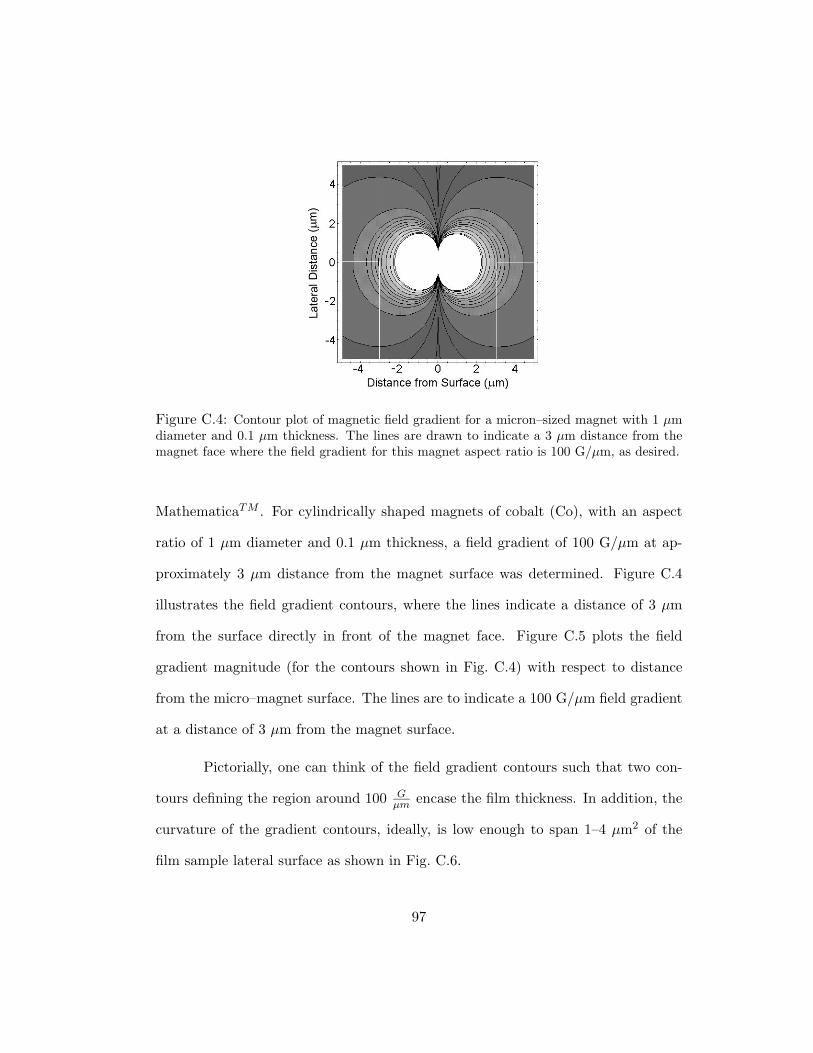
Figure C.4: Contour plot of magnetic field gradient for a micron–sized magnet with 1 µmdiameter and 0.1 µm thickness. The lines are drawn to indicate a 3 µm distance from themagnet face where the field gradient for this magnet aspect ratio is 100 G/µm, as desired.
MathematicaTM . For cylindrically shaped magnets of cobalt (Co), with an aspect
ratio of 1 µm diameter and 0.1 µm thickness, a field gradient of 100 G/µm at ap-
proximately 3 µm distance from the magnet surface was determined. Figure C.4
illustrates the field gradient contours, where the lines indicate a distance of 3 µm
from the surface directly in front of the magnet face. Figure C.5 plots the field
gradient magnitude (for the contours shown in Fig. C.4) with respect to distance
from the micro–magnet surface. The lines are to indicate a 100 G/µm field gradient
at a distance of 3 µm from the magnet surface.
Pictorially, one can think of the field gradient contours such that two con-
tours defining the region around 100 Gµm encase the film thickness. In addition, the
curvature of the gradient contours, ideally, is low enough to span 1–4 µm2 of the
film sample lateral surface as shown in Fig. C.6.
97
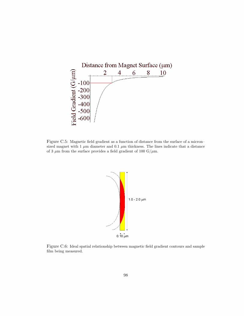
Figure C.5: Magnetic field gradient as a function of distance from the surface of a micron–sized magnet with 1 µm diameter and 0.1 µm thickness. The lines indicate that a distanceof 3 µm from the surface provides a field gradient of 100 G/µm.
Figure C.6: Ideal spatial relationship between magnetic field gradient contours and samplefilm being measured.
98
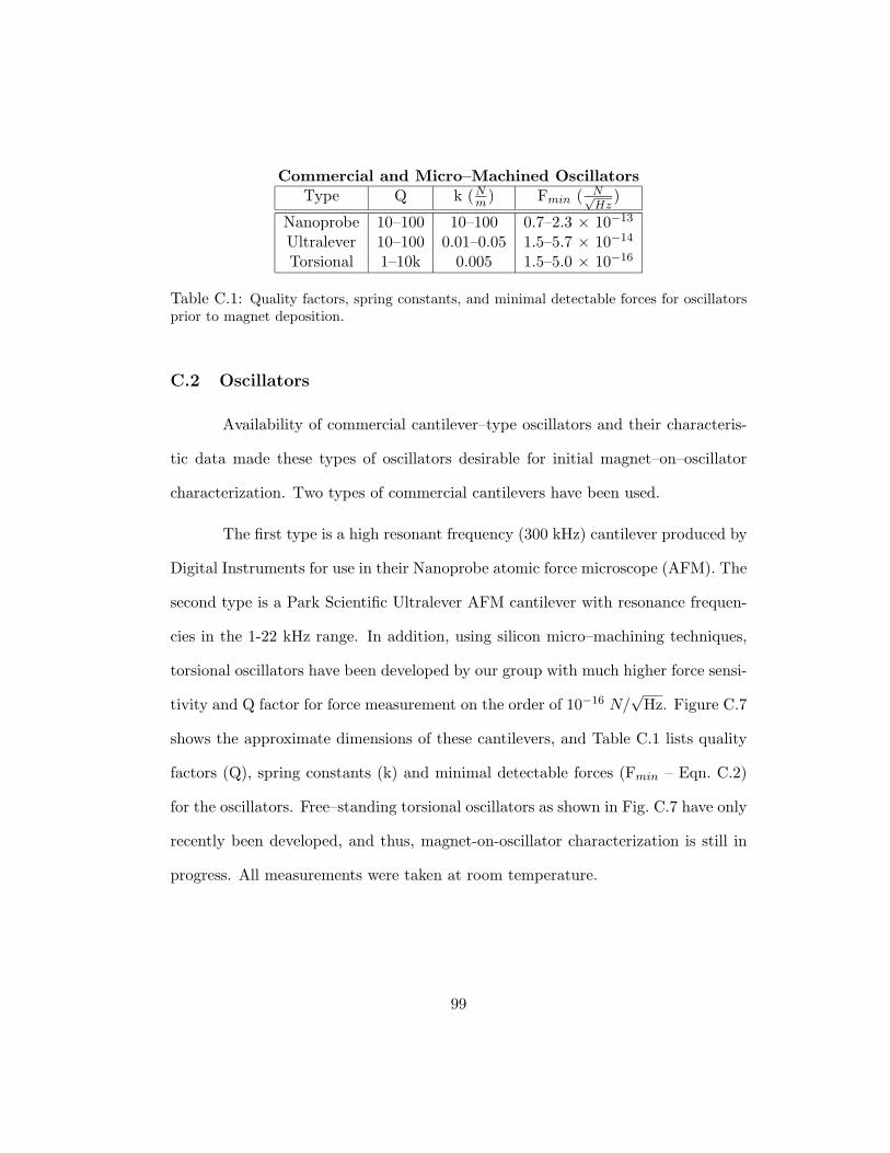
Commercial and Micro–Machined OscillatorsType Q k (N
m) Fmin ( N√Hz
)
Nanoprobe 10–100 10–100 0.7–2.3 × 10⁻¹³
Ultralever 10–100 0.01–0.05 1.5–5.7 × 10⁻¹⁴
Torsional 1–10k 0.005 1.5–5.0 × 10⁻¹⁶
Table C.1: Quality factors, spring constants, and minimal detectable forces for oscillatorsprior to magnet deposition.
C.2 Oscillators
Availability of commercial cantilever–type oscillators and their characteris-
tic data made these types of oscillators desirable for initial magnet–on–oscillator
characterization. Two types of commercial cantilevers have been used.
The first type is a high resonant frequency (300 kHz) cantilever produced by
Digital Instruments for use in their Nanoprobe atomic force microscope (AFM). The
second type is a Park Scientific Ultralever AFM cantilever with resonance frequen-
cies in the 1-22 kHz range. In addition, using silicon micro–machining techniques,
torsional oscillators have been developed by our group with much higher force sensi-
tivity and Q factor for force measurement on the order of 10−16 N/√
Hz. Figure C.7
shows the approximate dimensions of these cantilevers, and Table C.1 lists quality
factors (Q), spring constants (k) and minimal detectable forces (Fmin – Eqn. C.2)
for the oscillators. Free–standing torsional oscillators as shown in Fig. C.7 have only
recently been developed, and thus, magnet-on-oscillator characterization is still in
progress. All measurements were taken at room temperature.
99
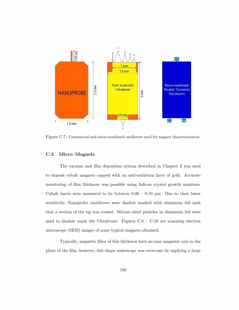
Figure C.7: Commercial and micro-machined oscillators used for magnet characterization.
C.3 Micro–Magnets
The vacuum and film deposition system described in Chapter 2 was used
to deposit cobalt magnets capped with an anti-oxidation layer of gold. Accurate
monitoring of film thickness was possible using Inficon crystal growth monitors.
Cobalt layers were measured to be between 0.06 – 0.10 µm. Due to their lower
sensitivity, Nanoprobe cantilevers were shadow masked with aluminum foil such
that a section of the tip was coated. Micron–sized pinholes in aluminum foil were
used to shadow mask the Ultralevers. Figures C.8 – C.10 are scanning electron
microscope (SEM) images of some typical magnets obtained.
Typically, magnetic films of this thickness have an easy magnetic axis in the
plane of the film, however, this shape anisotropy was overcome by applying a large
100
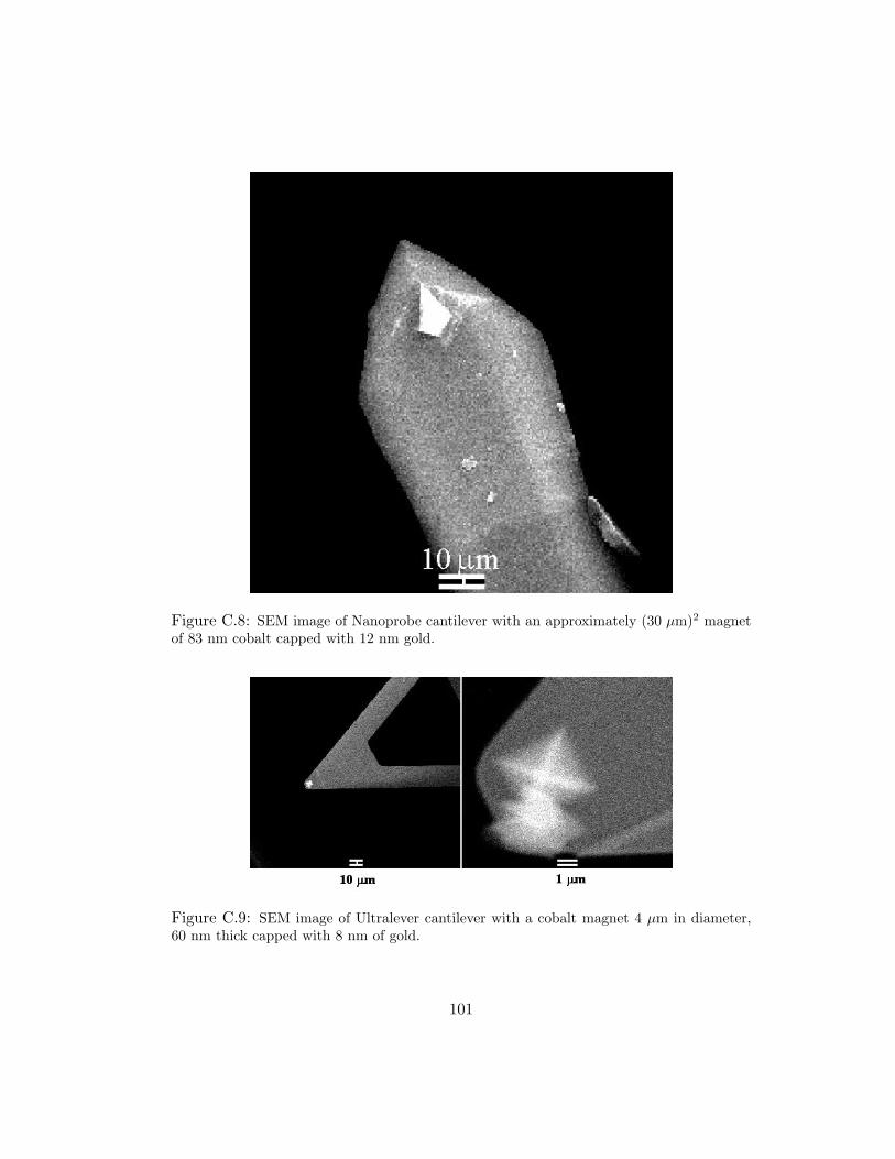
Figure C.8: SEM image of Nanoprobe cantilever with an approximately (30 µm)2 magnetof 83 nm cobalt capped with 12 nm gold.
Figure C.9: SEM image of Ultralever cantilever with a cobalt magnet 4 µm in diameter,60 nm thick capped with 8 nm of gold.
101
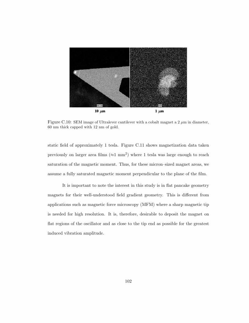
Figure C.10: SEM image of Ultralever cantilever with a cobalt magnet a 2 µm in diameter,60 nm thick capped with 12 nm of gold.
static field of approximately 1 tesla. Figure C.11 shows magnetization data taken
previously on larger area films (≈1 mm2) where 1 tesla was large enough to reach
saturation of the magnetic moment. Thus, for these micron–sized magnet areas, we
assume a fully saturated magnetic moment perpendicular to the plane of the film.
It is important to note the interest in this study is in flat pancake geometry
magnets for their well-understood field gradient geometry. This is different from
applications such as magnetic force microscopy (MFM) where a sharp magnetic tip
is needed for high resolution. It is, therefore, desirable to deposit the magnet on
flat regions of the oscillator and as close to the tip end as possible for the greatest
induced vibration amplitude.
102
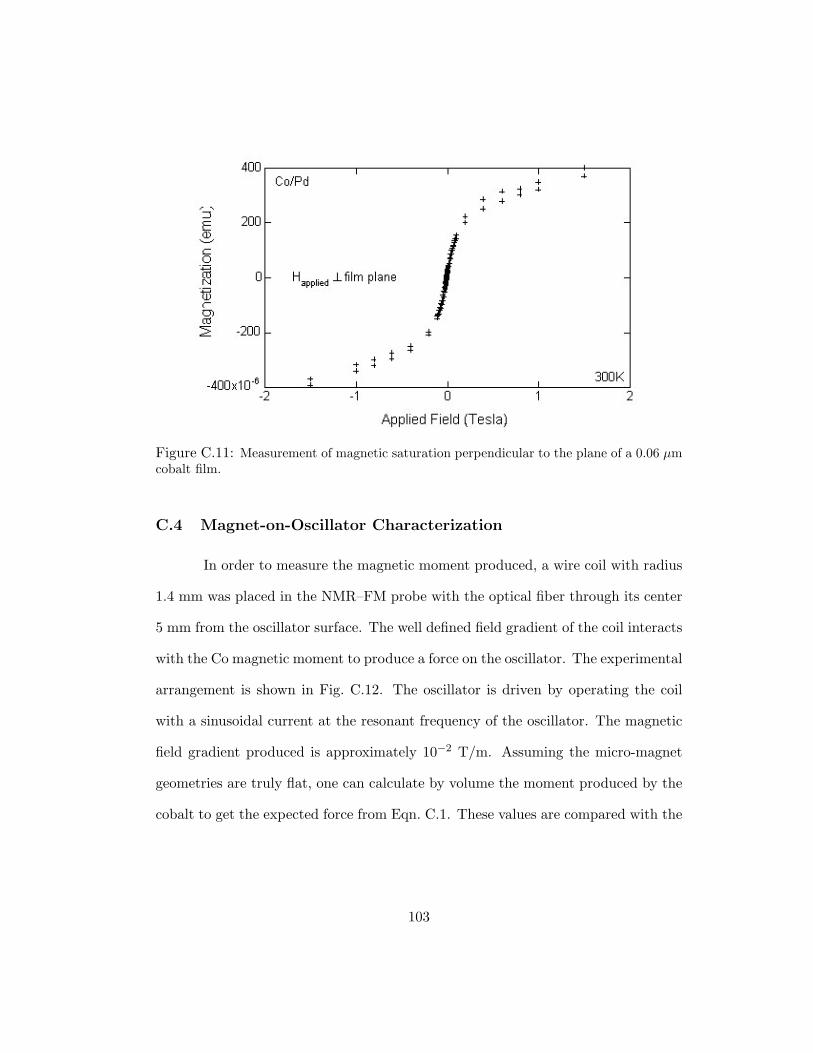
Figure C.11: Measurement of magnetic saturation perpendicular to the plane of a 0.06 µmcobalt film.
C.4 Magnet-on-Oscillator Characterization
In order to measure the magnetic moment produced, a wire coil with radius
1.4 mm was placed in the NMR–FM probe with the optical fiber through its center
5 mm from the oscillator surface. The well defined field gradient of the coil interacts
with the Co magnetic moment to produce a force on the oscillator. The experimental
arrangement is shown in Fig. C.12. The oscillator is driven by operating the coil
with a sinusoidal current at the resonant frequency of the oscillator. The magnetic
field gradient produced is approximately 10−2 T/m. Assuming the micro-magnet
geometries are truly flat, one can calculate by volume the moment produced by the
cobalt to get the expected force from Eqn. C.1. These values are compared with the
103
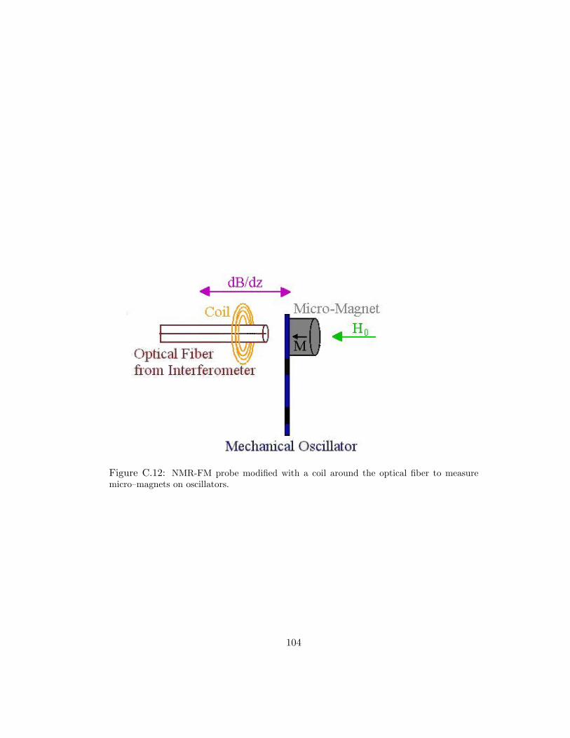
Figure C.12: NMR-FM probe modified with a coil around the optical fiber to measuremicro–magnets on oscillators.
104
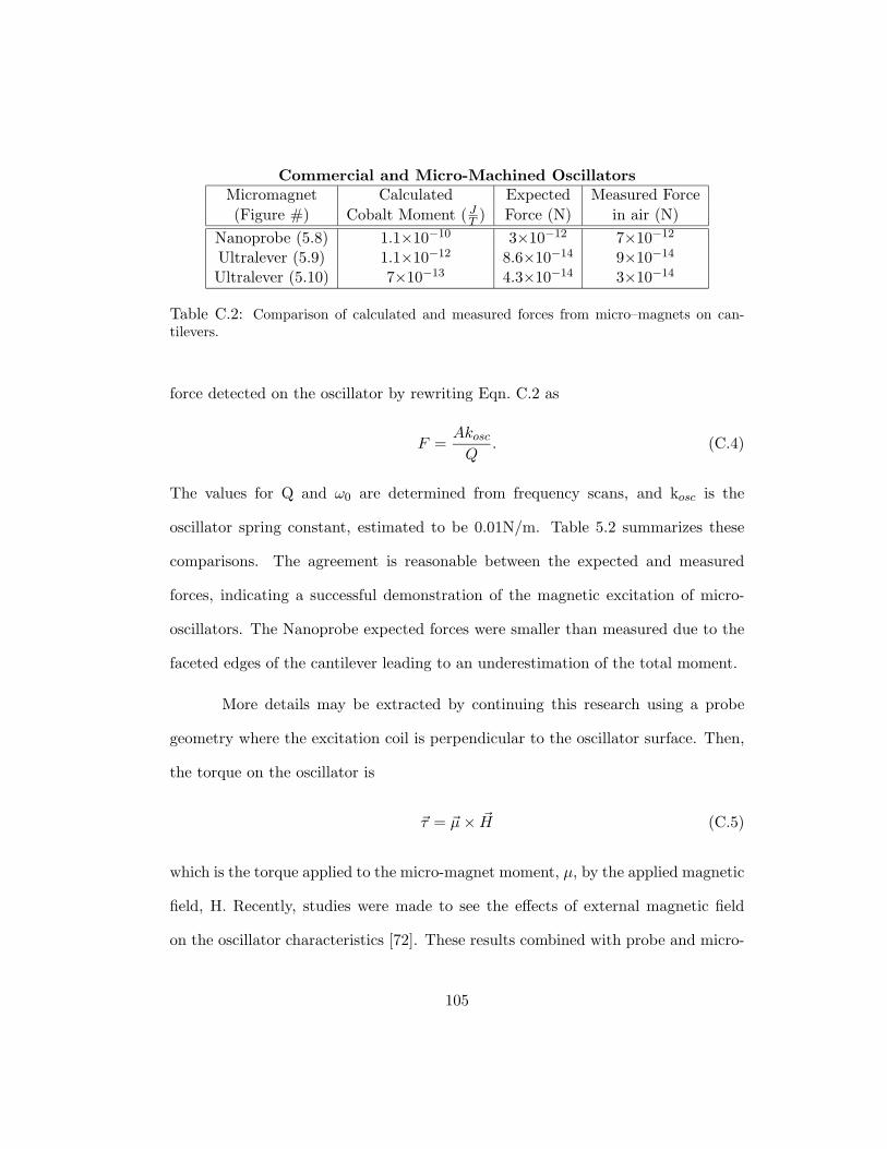
Commercial and Micro-Machined OscillatorsMicromagnet Calculated Expected Measured Force(Figure #) Cobalt Moment ( J
T ) Force (N) in air (N)Nanoprobe (5.8) 1.1×10⁻¹⁰ 3×10⁻¹² 7×10⁻¹²
Ultralever (5.9) 1.1×10⁻¹² 8.6×10⁻¹⁴ 9×10⁻¹⁴
Ultralever (5.10) 7×10⁻¹³ 4.3×10⁻¹⁴ 3×10⁻¹⁴
Table C.2: Comparison of calculated and measured forces from micro–magnets on can-tilevers.
force detected on the oscillator by rewriting Eqn. C.2 as
F =Akosc
Q. (C.4)
The values for Q and ω0 are determined from frequency scans, and kosc is the
oscillator spring constant, estimated to be 0.01N/m. Table 5.2 summarizes these
comparisons. The agreement is reasonable between the expected and measured
forces, indicating a successful demonstration of the magnetic excitation of micro-
oscillators. The Nanoprobe expected forces were smaller than measured due to the
faceted edges of the cantilever leading to an underestimation of the total moment.
More details may be extracted by continuing this research using a probe
geometry where the excitation coil is perpendicular to the oscillator surface. Then,
the torque on the oscillator is
τ = µ × H (C.5)
which is the torque applied to the micro-magnet moment, µ, by the applied magnetic
field, H. Recently, studies were made to see the effects of external magnetic field
on the oscillator characteristics [72]. These results combined with probe and micro-
105

magnet improvements indicate readiness of our NMR force microscopy for solid-state
applications.
106
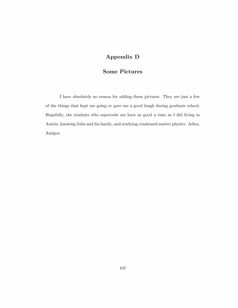
Appendix D
Some Pictures
I have absolutely no reason for adding these pictures. They are just a few
of the things that kept me going or gave me a good laugh during graduate school.
Hopefully, the students who supercede me have as good a time as I did living in
Austin, knowing John and his family, and studying condensed matter physics. Adios,
Amigos.
107
Figure D.1: Troy speaking at the Metal Hydrides conference (MH2002) in Annecy, France.
108
Figure D.2: Troy marrying Jodi at his parents’ house in Rockwall, Texas, April 7, 2001.
109
Figure D.3: Troy showing off his super-cool boron tattoo.
110
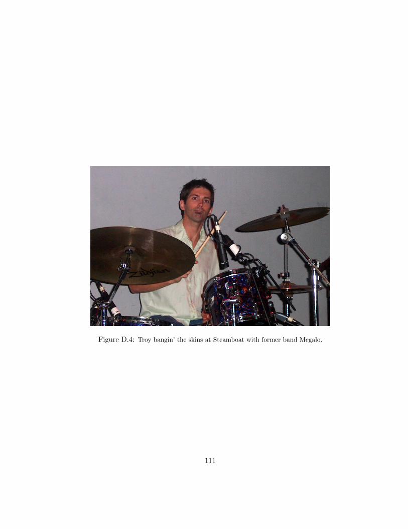
Figure D.4: Troy bangin’ the skins at Steamboat with former band Megalo.
111
Figure D.5: Signature page for this dissertation.
112
Bibliography
[1] T. Graham, Philos. Trans. Roy. Soc. London 156, 399 (1866).
[2] J.N. Huiberts, R. Griessen, J.H. Rector, R.J. Wijngaarden, D.G. de Groot,
and N.J. Koeman, Nature 380, 231 (1996).
[3] M. Ouwerkerk, Electrochemical Hydrogen Storage Properties of Magnesium-
Scandium Hydride Thin Films and Powders, Philips Research presentation,
Gordon Conference (2001).
[4] R. Griessen et al., J. Alloys Comp. 253-254 44, (1997).
[5] S.J. van der Molen, M.S. Welling, and R. Griessen, Phys. Rev. Lett. 85, 3882
(2000).
[6] A. T. M. van Gogh, Doctoral dissertation Probing the Metal-Insulator Transis-
tion in Rare–Earth Based Switchable Mirrors, (Vrije Universiteit, Amsterdam,
2001).
[7] M. L. Lieberman and P. G. Wahlbeck, J. Phys. Chem. 69, 3973 (1965).
[8] M. L. Lieberman and P. G. Wahlbeck, J. Phys. Chem. 69, 3514 (1965).
[9] M. L. Lieberman and P. G. Wahlbeck, J. Phys. Chem. 69, 2510 (1965).
[10] M. Kremers et al., Phys. Rev. B 57, 4943 (1998).
113
[11] J. N. Huiberts et al., J. Alloys Comp. 239, 158 (1996).
[12] S. J. van der Molen et al., J. Appl. Phys. 86, 6107 (1999).
[13] A. F. Th. Hoekstra et al., Phys. Rev. Lett. 86, 5349 (2001).
[14] L. Schlapbach, ed., Hydrogen in Intermetallic Compounds (Springer, Berlin,
1988).
[15] P. Vajda, “Hydrogen in Rare-Earth Metals, Including RH2+x Phases” in Hand-
book on the Physics and Chemistry of Rare Earths, Vol. 1 (Elsevier, 1995).
[16] Ibid, Vol. 8, p.1-161.
[17] Ibid, Vol. 20, p.105-291.
[18] Ibid, Vol. 27, p.339-533.
[19] R. M. Cotts, in Hydrogen in Metals I, G. Alefeld and J. Volkl, eds. (Springer,
1978), p.227.
[20] B. Y. Kotur and E. Gratz “Scandium Alloy Systems and Intermetallics” in
Handbook on the Physics and Chemistry of Rare Earths, K. A. Gschneidner,
Jr. and L. Eyring, eds. vol. 27 (North-Holland, 1999), p.339-533.
[21] P. J. Kelly, J. P. Dekker, R. Stumpf, Phys. Rev. Lett. 78, 1315 (1997).
[22] Y. Wang, M. Y.Chou, Phys. Rev. B 51, 7500 (1995).
[23] K. K. Ng, F. C. Zhang, V. I. Anisimov, T. M. Rice, Phys. Rev. Lett. 78, 1311
(1997).
114
[24] A. T. M. van Gogh and R. Griessen, J. Alloys Comp., 330-332, 338 (2002).
[25] A. T. M. van Gogh, D. G. Nagengast, E. S. Kooij, N. J. Koeman, J. H. Rector,
and R. Griessen, Phys. Rev. B 63, 195105 (2001).
[26] MDI Jade software package for pattern analysis and phase identification, Ma-
terials Data Inc., Livermore, CA, USA.
[27] P. van Gelderen and P. J. Kelly and G. Brocks, and R. Stumpf, Phys. Rev. B,
63, 100301 (2001).
[28] M. Rode et al., Phys. Rev. Lett. 78, 1315 (1997).
[29] D. G. Nagengast et al., Appl. Phys. Lett. 75, 2050 (1999).
[30] I. A. M. E. Geibels et al., J. Alloys Comp. 330, 875 (2002).
[31] J. Isidorsson et al., Electrochimica Acta 46, 2179 (2001).
[32] J. W. J. Kerssemakers et al., Nature 406, 489 (2000).
[33] F. J. A. den Broeder et al., Nature 394, 656 (1998).
[34] A. T. M. van Gogh et al., Appl. Phys. Lett. 77, 815 (2000).
[35] A. T. M. van Gogh, E. S. Kooij, and R. Griessen, Phys. Rev. Lett. 83, 4614
(1999).
[36] J. N. Huibertset al., Phys. Rev. Lett. 79, 3724 (1997).
[37] P. L. Notten, M. Kremers, and R. Griessen, J. Electrochem. Soc. 143, 3348
(1996).
115
[38] E. S. Kooij, A. T. M. van Gogh, and R. Griessen, J. Electrochem. Soc. 146,
2990 (1999).
[39] T. C. Messina, C. W. Miller, and J. T. Markert”, J. Alloys Comp., in press
(2003).
[40] H. Kierey et al., Phys. Rev. B 63, 134109 (2001).
[41] A. C. Switendick, J. of Less Common Metals 74, 199 (1980).
[42] J. H. Weaver and D. T. Peterson, J. of Less Common Metals 74, 207 (1980).
[43] C. L. Jensen and M. P. Zalesky, J. of Less Common Metals 75, 197 (1980).
[44] J. W. Ross and L. L. Isaacs, J. Phys. Chem. Solids 31, 747 (1970).
[45] Z. Fisk and D. C. Johnston, Phys. Lett. 53A, 39 (1975).
[46] M. Jerosch-Herold et al., Z. Naturforsch 40a, 222 (1984).
[47] R. B. McLellan and R. Kirchheim, J. Phys. Chem. Solids 41, 1241 (1980).
[48] A. E. Curzon and O. Singh, J. Phys. F: Metal Phys. 8, 1619 (1978).
[49] A. E. Curzon and O. Singh, Thin Solid Films 57, 157 (1979).
[50] S. J. van der Molen, M. S. Welling, and R. Griessen, Pys. Rev. Lett. 85, 3882
(2000).
[51] A. T. M. van Gogh et al., Phys. Rev. Lett. 85, 2156 (2000).
[52] J. Shinar, B. Dehner, B. J.Beaudry, and D. T. Peterson, Phy. Rev. B 37, 2066
(1988).
116
[53] J. Shinar, B. Dehner, R. G. Barnes, and B. J. Beaudry, Phys. Rev. Lett. 64,
563 (1990).
[54] CRC Handbook of Chemistry and Physics (CRC, Boca Raton, 1987-88), 68th
edition.
[55] S. L. Altmann and C. J. Bradley, Proc. Phys. Soc. 92, 764 (1967).
[56] G. S. Fleming and T. L. Loucks, Phys. Rev. 173, 685 (1968).
[57] S. Mahmoud and Z. S. El Mandouh, J. of Materials Science 22, 651 (1987).
[58] M. Sigrist et al., Phys. Rev. B 35, 3760 (1987).
[59] D. A. Gorodetskii and A. A. Yask’ko, Soviet Physics-Solid State 11, 2028
(1970).
[60] R. Ahuja, B. Johansson, J. M. Wills, and O. Eriksson, Appl. Phys. Lett. 71,
3498 (1997).
[61] E. J. Johnson in Semiconductors and Semimetals, eds. R. K. Willardson and
C. Beer (Academic Press, New York, 1967), v. 3.
[62] D. Rugar, O. Zugar, S. Hoen, C.S. Yannoni, H.-M. Vieth, and R.D. Kendrick,
Science 264, 1560 (1994).
[63] J. A. Sidles, Appl. Phys. Lett. 58, 2854 (1991).
[64] K. Wago, D. Botkin, C. S. Yannoni, and D. Rugar, Phys. Rev. B 57, 1108,
(1998).
117
[65] J. A. Sidles, et al., Rev. Mod. Phys. 67, 249 (1995).
[66] D. Rugar, C. S. Yannoni, and J. A. Sidles, Nature 360, 563 (1992).
[67] T. A. Barrett, Experimental Considerations for the Development of a Nu-
clear Magnetic Resonance Force Microscope, Ph.D. Dissertation, University
of Texas at Austin, Department of Physics, (1999).
[68] M. D. Chabot, Force Detection of Nuclear Magnetic Resonance using Double-
Torsional Micro-Oscillators, Ph.D. Dissertation, University of Texas at Austin,
Department of Physics, (2001).
[69] T. Graf, Interferometry on High-Q Double-Torsional Oscillators for the Study
of Vortices in in Type-II Superconductors, Master of Science Thesis, University
of Texas at Austin, Department of Physics, (1998).
[70] M. D. Chabot and J. T. Markert, Proc. SPIE 3875, 104 (1999).
[71] M. D. Chabot, T. C. Messina, V. Mancevski, C. W. Miller, and J. T. Markert,
Proc. SPIE 4559, 24 (2001).
[72] C. W. Miller, U. M. Mirsaidov, T. C. Messina, Y. J. Lee, and J. T. Mark-
ert, 47th Annual Conference on Magnetism and Magnetic Materials, Tampa,
Florida, USA, 2002, to be published in J. Appl. Phys. May 2003.
[73] E. Hecht, “The Diffraction Grating” in Optics, 3rd ed. (Addison-Wesley, Mas-
sachusetts, 1998), p.465–72.
118
[74] T. C. Messina, Design, Construction, and Characterization of an Ultra-High
Vacuum System for Synthesis of Magnetic Thin Films, Master of Arts Thesis,
University of Texas at Austin, Department of Physics, (1999).
[75] C. Kittel, Introduction to Solid State Physics, 6th ed. (John Wiley and Sons,
Inc., New York, 1998), p.49.
[76] T. B. Massalski et al., Binary alloy phase diagrams, (American Society for
Metals, Ohio, 1986), CD-ROM.
119
Publications
Invited Talks
• T. C. Messina, C. W. Miller, J. T. Markert, “Steric Effects in the Metal-
Insulator (Mirror-Transparent) Transition in YHx,” University of Texas at
Austin, Graduate Student Lecture Series, September 17, 2002.
Talks, Posters, and Presentations
• T. C. Messina, C. W. Miller, J. T. Markert, “Optical Switching, Structure,
and Transport in Y-Sc Hydride Thin Films,” American Physical Society March
Meeting 2002, Indianapolis, IN, USA, 18-22 March 2002.
• J. T. Markert, G. I. Drandova, T. C. Messina, “NMR of 89Y in the Copper-
Oxide Spin-Chain Compound Ca2+xY2−xCu5O10,” American Physical Society
March Meeting 2002, Indianapolis, IN, USA, 18-22 March 2002.
• C. W. Miller, M.D. Chabot, T. C. Messina, Y.J. Lee, J.T. Markert, “Nuclear
Magnetic Resonance Force Microscopy Using Single-Crystal Silicon Double-
Torsional Micro-Oscillators,” American Physical Society March Meeting 2002,
Indianapolis, IN, USA, 18-22 March 2002.
• T. C. Messina, M. D. Chabot, K. T. Tatebe, U. Mirsaidov, A. Badinski,
and J. T. Markert, “Magnet-on-Oscillator Characterization for Nuclear Mag-
netic Resonance Force Microscopy,” American Physical Society March Meeting
120
2001, Seattle, WA, USA, 12-16 March 2001.
• P. S. Lysaght, R. Bergmann, J. Chen, T. Messina, R. Murto, D. Sing, and
H. R. Huff, “Experimental Observations of the Thermal Stability of High-κ
Gate Dielectric Materials on Silicon,” Abstract for the 2001 meeting of the
Materials Research Society (E-MRS).
• J. T. Markert, K. Mochizuki, T. C. Messina, E. E. Judge, (University of Texas
at Austin), B. Dam, J. Huijbregste, J. H. Rector, M. Vreeken, R. Griessen (In-
stitute COMPAS, Faculty of Physics and Astronomy, Vrije University, Amster-
dam, the Netherlands), “Thin Films of Infinite-Layer Sr1−xLaxCuO2 Grown
by Laser Ablation,” Abstracts of the 1998 March Meeting of the American
Physical Society, Los Angeles, CA (1998)
• E. E. Judge, K. Mochizuki, T. C. Messina, J. T. Markert (University of Texas
at Austin), B. Dam, J. Huijbregste, J. H. Rector, M. Vreeken, R. Griessen (In-
stitute COMPAS, Faculty of Physics and Astronomy, Vrije University, Am-
sterdam, the Netherlands), “Hall Effect and Post-Annealing of Thin Films
of Infinite-Layer Sr1−xLaxCuO2,” American Physical Society March Meeting
1998, Los Angeles, CA (1998)
• J.T. Markert, B.C. Dunn, T.C. Messina, M.M. Maedgen, “Magnetism, Struc-
ture, and Resistivity of the Lithium-Doped T’-Phase: Gd2Cu1−xLixO4−d and
Nd2−yCeyCu1−xLixO4−d,” Abstracts of the 5th International Conference on
Materials and Mechanisms of Superconductivity - High Temperature Super-
conductivity (M2S-HTSC-V), Beijing, China, 28 February - 4 March 1997.
121
• J.T. Markert, K. Mochizuki, T.C. Messina, “Extreme Low Amplitude Vortex
Dissipation Study of Single Crystal YBa2Cu3O7−d Using High-Q Mechani-
cal Oscillators,” Abstracts of the 5th International Conference on Materials
and Mechanisms of Superconductivity - High Temperature Superconductivity
(M2S-HTSC-V), Beijing, China, 28 February–4 March 1997.
Articles
• C.W. Miller, U. Mirsaidov, T.C. Messina, J.T. Markert, “External Field Ef-
fects on Characteristics of Magnetically-Capped Oscillators for Magnetic Res-
onance Force Microscopy,” 47th Annual Conference on Magnetism and Mag-
netic Materials, Tampa, Florida, USA, 2002, to be published in Journal of
Applied Physics May 2003.
• T. C. Messina, C. W. Miller, J. T. Markert, “Steric Effects in the Metal-
Insulator (Mirror-Transparent) Transition in YHx,” J. Alloys and Compounds
- Proceedings for MH2002, Annecy, France, 2002 (in press).
• J.T. Markert, T.C. Messina, B. Dam, J. Huijbregste, J.H. Rector, and R.
Griessen, “Infinite-Layer Copper-Oxide Laser-Ablated Thin Films: Substrate,
Buffer-Layer, and Processing Effects,” Applied Superconductivity Conference,
Houston, Texas, USA, 2002, to be published in IEEE Transactions on Applied
Superconductivity 2003.
• G. I. Drandova, T. C. Messina, J. T. Markert, “NMR of 89Y in the Copper-
Oxide Spin-Chain Compound Ca2+xY2−xCu5O10,” Proceedings of the 2002
122
International Conference on Metal and Oxide Superconductors, Hsinchu, Tai-
wan, 2002 (in press).
• K. Mochizuki, J.-H. Choi, T. C. Messina, Y. Ando, K. Nakamura, J. T. Mark-
ert, “Extreme Smallness of the Transverse Force on Moving Vortices,” LT23
Proceedings, Japan, 2002 (in press).
• J. Barnett, D. Riley, T. Messina, P. Lysaght, “Wet Etch Enhancement of
HfO2 Films by Implant Processing,” UCPSS-2002, Proceedings of the Sixth
International Symposium on Ultra-Clean Silion Surfaces (Scitec Publications
Ltd, Zurich, Switzerland, 2002), special edition of Solid State Phenomena (in
press).
• P. S. Lysaght, P. J. Chen, R. Bergmann, T. Messina, R. W. Murto and H.
R. Huff, “Experimental Observations of the Thermal Stability of High-κ Gate
Dielectric Materials on Silicon,” Journal of Non-Crystalline Solids, vol. 303,
no. 1, 54-63 (2002).
• M. D. Chabot, T.C. Messina, V. Manicevski, C. W. Miller, J. T. Markert,
“Single-Crystal Silicon Triple-Torsional Micro-Oscillators for Use in Magnetic
Resonance Force Microscopy,” Proceedings of SPIE, San Jose, CA, USA, Oc-
tober 2001.
• J. T. Markert, T. C. Messina, B. Dam, J. Huijbregste, J. Rector, R. Griessen,
“Observation of Step-Flow Growth in Laser-Ablated thin films of the T’-Phase
compound Pr2CuO4,” Physica C, 341-348, 2355-56 (2000).
123
• J. T. Markert, T. C. Messina, B. Dam, J. Huijbregste, J. H. Rector, R.
Griessen, “Laser-Ablated Thin Films of Infinite-Layer Compounds and Re-
lated Materials,” Proceedings of SPIE, Orlando, FL, USA, 24-28 April 2000,
p.141.
• T. Ono, G. A. Rozgonyi, C. Au, T. C. Messina, R. Goodall, H. R. Huff, “Oxy-
gen Precipitation Behavior in 300mm Polished Czochralski Silicon Wafers,” J.
Electrochem. Soc. 146, 3807 (1999).
• H. R. Huff, D. McCormack Jr., C. Au, T. C. Messina, K. Chan, R. Goodall,
“Current Status of 200mm and 300mm Silicon Wafers,” Proceedings of the
Intl. Solid State Devices and Materials (ISSDM ’97), Japan, p. 456 and
Conference Abstracts p.575, (1997) also published in Jpn J. Appl Phys, 37,
(1998) Pt.1, No.3B.
• C. Au, T. C. Messina, R. Goodall, H. R. Huff, “Characterization of 300mm
Polished Silicon Wafers,” Proceedings of the 8th International Symposium on
Silicon Materials and Technology, v.1, p.641, (1998).
• T. C. Messina, C. Au, S. Shih, Z. Yang, R. Goodall, H. R. Huff, “Current Sta-
tus of 300mm Wafer Characterization,” Proceedings of the International Me-
chanical Engineering Conference and Exposition (IMECE ’98), p.825, (1998).
• S. Shih, C. Au, Z. Yang, T. C. Messina, R. Goodall, H. R. Huff, “Characteriza-
tion of 300mm Silicon-Polished and Epi Wafers,” Proceedings of the E-MRS,
(1998).
124
• J. T. Markert, K. Mochizuki, T. C. Messina, B. C. Dunn, A. V. Elliott, “Stud-
ies of Infinite-Layer, T’-Phase, and 1-D Ladder Copper-Oxide Compounds,”
Proceedings of the NATO Advanced Research Workshop: Physics and Materi-
als Science in High Temperature Superconductivity IV, Strbske Pleso, Slovak
Republic, 21-27 July 1996.
125
Vita
Troy Christopher Messina was born in Dallas, Texas on August 30, 1973,
the son of Darlene Joy Messina and Robert Logan Messina. After graduating from
Rockwall High School, Rockwall, Texas, in 1991, he attended the University of
Texas at Austin for one year. Then, he relocated to Dallas and attended Richland
Community College for a year and a half before returning to UT Austin in January
of 1994. He graduated from UT in May, 1996, with a Bachelor of Science degree in
physics. In January of 1997, he entered The Graduate School of The University of
Texas at Austin, receiving a Master of Arts in physics in December of 1999. Two
years after meeting, Troy married Jodi Moore, the woman of his dreams, on April 7,
2001. He has also been a professional drummer/percussionist for Half Street, Speer,
the Neal Kassanoff Trio, 3 Penny Opera, Megalo, and Chester.
Permanent address: 1414 Larkwood DriveAustin, Texas 78723
This dissertation was typeset with LATEX† by the author.
†LATEX is a document preparation system developed by Leslie Lamport as a special version ofDonald Knuth’s TEX Program.
126


![Dr. Brian-Christopher “BC” Farnham - Troy University · Dr. Brian-Christopher “BC” Farnham ... supervision of Dr. Nathaniel Fox] ... Farnham, BC., Pugh, E., Carpenter, J.,](https://img.pdfslide.us/doc/110x75/5b5ce0377f8b9a16498cf12c/dr-brian-christopher-bc-farnham-troy-university-dr-brian-christopher.jpg)