Embed Size (px)
Citation preview

©Copyright 2013
Apsara Ravish Suvarna
Transformer-Based Tunable Matching Networks
implemented in Silicon CMOS
Apsara Ravish Suvarna
A thesis
submitted in partial fulfillment of the
requirements for the degree of
Master of Science in Electrical Engineering
University of Washington
2013
Committee:
Jacques Christophe Rudell
Robert Bruce Darling
Program Authorized to offer degree:
Department of Electrical Engineering

In presenting this thesis in partial fulfillment of the requirements for a master’s degree at the
University of Washington, I agree that the library shall make its copies freely available for
inspection. I further agree that extensive copying of this thesis is allowable only for scholarly
purposes, consistent with ‘fair use’ as prescribed in the U.S. Copyright Law. Any other
reproduction for any purposes or by any means shall not be allowed without my written
permission.
Signature
Date
i
University of Washington
Abstract
Transformer-Based Tunable Matching Networks
implemented in Silicon CMOS
Apsara Ravish Suvarna
Chair of the Supervisory Committee:
Professor Jacques C. Rudell
Department of Electrical Engineering
The growing market for small form-factor, low power wireless communication devices has
provided tremendous impetus towards research on multi-mode and multi-standard transceiver
designs. A key building block in realizing such a transceiver is a reconfigurable/tunable
matching network. In this thesis, two tunable matching networks, designed with the explicit goal
of providing large impedance-tunability and low insertion loss, at a fixed resonant frequency
have been proposed. The two tunable networks, namely Transformer-plus-L-Match Network
(TLMN) and Transformer-plus-Pi-Match Network (TPMN) are fully-integrated and prototype
test-chips have been realized in a 40nm bulk CMOS process. The transformer in the two
networks provides fixed impedance conversion and switch-capacitance based L/Pi-network
provides a variable impedance transformation. A design methodology highlighting the loss
mechanism in a transformer-based matching network is presented. Based on this methodology,
circuit conditions to obtain minimum insertion loss are derived.
ii
Table of Contents
Table of Contents ........................................................................................................................ ii
List of Figures ............................................................................................................................ iv
List of Tables .............................................................................................................................. vi
1. Introduction ................................................................................................................................. 1
2. Matching Networks for Integrated CMOS Power Amplifiers .................................................... 4
2.1 Optimal Load for a PA ................................................................................................. 4
2.2 Basic Types of Matching Networks ............................................................................. 6
2.3 Advantages of Tunable Matching Networks in Power Amplifiers .............................. 9
2.3.1 Power Requirements and Ropt values in different standards ............................... 11
2.3.2 AM-PM Conversion in Power Amplifiers .......................................................... 12
2.4 Challenges in Tunable Matching Network Design..................................................... 13
3. Transformer-Based Matching Networks ................................................................................... 16
3.1 Transformer model ..................................................................................................... 17
3.2 Transformer matching network design to minimize insertion loss ............................ 19
3.3 Validation of the transformer-matching network model ............................................ 25
3.4 Parallel secondary capacitor vs. Series secondary capacitor ...................................... 28
4. Tunable Matching Network Design .......................................................................................... 31
4.1 Transformer-plus-L-match-based tunable Matching Network (TLMN) .................... 33
iii
4.1.1 Design details ............................................................................................................ 34
4.1.2 Tuning Range Limitations using an L-match ........................................................... 37
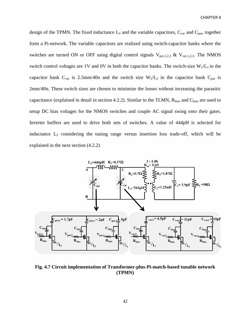
4.2 Transformer-plus-Pi-match-based tunable Matching Network (TPMN) ................... 41
4.2.1 Design details ............................................................................................................ 41
4.2.2 Tuning Range Limitations using a Pi-match ............................................................ 43
4.3 Comparison between TLMN and TPMN ........................................................................ 46
5. Simulation Results .................................................................................................................... 50
5.1 Simulation results of the TLMN ...................................................................................... 51
5.2 Simulation results of the TPMN ...................................................................................... 54
5.3 Comparison of results of the TLMN and TPMN ............................................................ 57
6. Conclusion ................................................................................................................................ 58
References ................................................................................................................................. 60
iv
List of Figures
Fig. 2.1 Concept of optimum load impedance in an ideal class-A PA [9] ..................................... 6
Fig. 2.2 Impedance Down-conversion Networks (a) High Pass Network (b) Low Pass Network . 7
Fig. 2.3 Impedance Up-conversion Networks (a) Low Pass Network (b) High Pass Network ...... 8
Fig. 2.4 Transformer as an Impedance Scaling Network................................................................ 9
Fig. 3.1 Frequency-dependent lumped element model for transformer [25] ................................ 17
Fig. 3.2 Low frequency approximation of broadband model for transformer .............................. 18
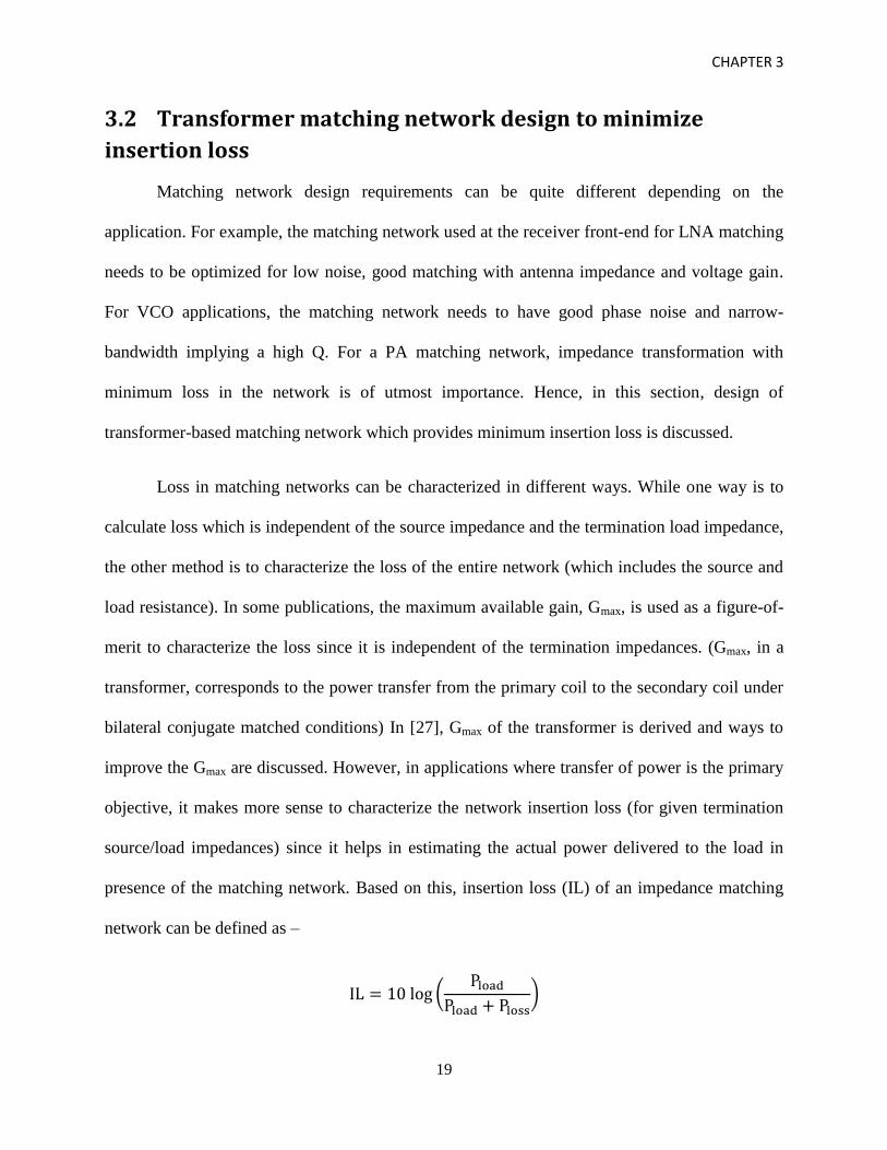
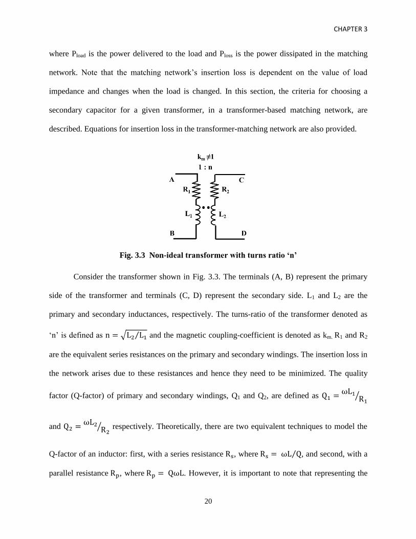
Fig. 3.3 Non-ideal transformer with turns ratio ‘n’ ..................................................................... 20
Fig. 3.4 Equivalent circuit of a loaded transformer with impedances reflected onto primary side
............................................................................................................................................. 21
Fig. 3.5 Steps involved in simplifying a transformer with parallel secondary capacitor and load
RL ......................................................................................................................................... 22
Fig. 3.6 (a) Matlab plot of M=RL,eff / (R2,eff + R1) Vs. C2 (b) Plot of insertion loss (IL) Vs. C2 .. 26
Fig. 3.7 Plot of insertion loss Vs. freq. in a transformer with series/parallel secondary capacitors
............................................................................................................................................. 30
Fig. 4.1 Tunable Matching network implemented with transformer and L/Pi- network .............. 32
Fig. 4.2 Circuit implementation of Transformer-plus-L-match-based tunable network (TLMN) 35
Fig. 4.3 Simplified representation of the TLMN .......................................................................... 36
Fig. 4.4 Illustration of tuning range limitation due to Cvar and Cpar values ................................... 39
Fig. 4.5 (a) Switch-capacitor branch (b) Equivalent circuit when the switch is in ‘ON’ state .... 40
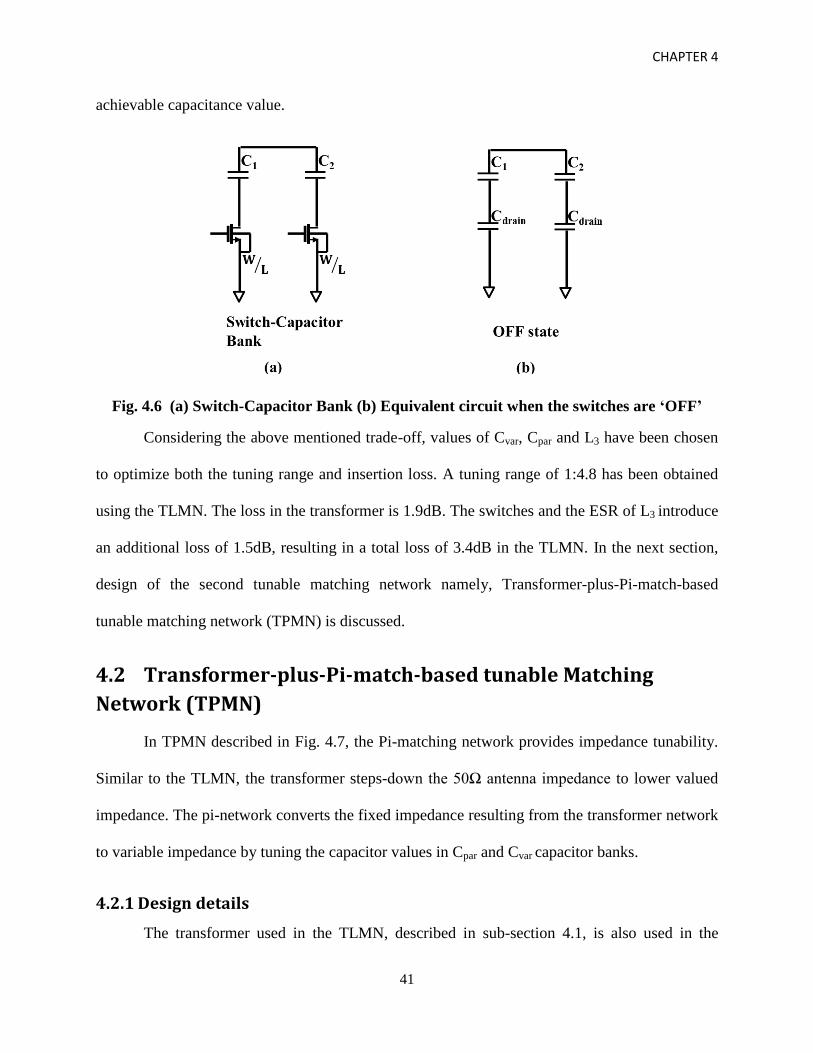
Fig. 4.6 (a) Switch-Capacitor Bank (b) Equivalent circuit when the switches are ‘OFF’ ........... 41
Fig. 4.7 Circuit implementation of Transformer-plus-Pi-match-based tunable network (TPMN) 42
Fig. 4.8 Simplified representation of the TPMN .......................................................................... 43
v
Fig. 4.9 Tuning Range Limitation in the TPMN: Plot of (a) Real (Zin) Vs. Cvar (b) Cpar required to
resonate the imaginary part of Yin Vs. Cvar (c) Insertion Loss Vs. Cvar – for different values
of L3 ..................................................................................................................................... 44
Fig. 4.10 Limitation in the TLMN due to parasitic capacitances ................................................. 48
Fig. 4.11 Cross-section of a NMOS transistor in deep n-well ...................................................... 48
Fig. 5.1 Layout of (a) TLMN (b) TPMN ...................................................................................... 50
Fig. 5.2 Plot of |Zin| and phase (Zin) Vs. frequency for different switch settings in the TLMN ... 52
Fig. 5.3 Plot of Power gain as a function of input power in the TLMN ....................................... 54
Fig. 5.4 Plot of |Zin| and phase (Zin) Vs. frequency for different switch settings in the TPMN .... 55
Fig. 5.5 Plot of Power gain as a function of input power in the TPMN ....................................... 56

vi
List of Tables
Table 5.1 Insertion Loss and phase of S21 across Zin values in the TLMN .................................. 52
Table 5.2 Insertion Loss and phase of S21 across Zin values in the TPMN ................................... 55
Table 5.3 Comparison of the performance of TLMN and TPMN ................................................ 57
CHAPTER 1
1
1. Introduction
The expanding market for small form-factor, low-power wireless communication
devices, such as cellular-phones, laptops, and tablets, has provided tremendous impetus towards
research on multi-mode and multi-standard transceiver designs. The immediate-next goal in
these wireless state-of-the-art devices will be to incorporate multiple radios on a single chip in
order to satisfy the consumer’s short/long-range high-speed/low-power data-transfer
requirements. Software defined radio (SDR), wherein a single transceiver chip can be configured
to talk with Wi-Fi, GSM or even Bluetooth peripherals has the potential to enable substantial
reduction in the size of these devices. However, while the digital backend can be highly
programmable and is well suited for ‘software-defined’ re-configurability, the analog front-end is
traditionally designed and optimized for a single carrier frequency ( ) and peak output power.
Analog circuits are tuned at with the help of matching networks comprising of inductors,
capacitors and transformers in order to maximize the power-gain at radio-frequencies. Thus,
single chip SDR, which entails processing signals over a large range of carrier-frequencies,
bandwidths, and power-levels would significantly benefit by advances in reconfigurable/tunable
matching network design.
A matching network with a reconfigurable impedance transformation ratio opens the door
to several other applications as well. One such example is a long-range sensor power-amplifier
that is required to maintain constant output-power under the influence of a variable supply
voltage. Consider a long-range sensor PA that employs a switching amplifier in the final stage to
get good efficiency. Since the power output in switching amplifiers is proportional to
CHAPTER 1
2
( )
⁄ by varying Rload as the supply voltage varies, the output power can be
maintained at a constant value [1]. Tunable matching networks can also be employed in systems
to improve the performance significantly. Consider a transmitter used in a mobile phone
application. The antenna impedance is nominally assumed to be 50Ω but variations as large as
1:7 can occur in the impedance (real and imaginary part) owing to varying environmental
conditions [2]. This can lead to degraded performance in addition to causing large voltage-
standing wave-ratio (VSWR) variation at PA-antenna interface which could potentially damage
the PA [3], [4]. While this problem could be solved by placing isolators between the PA and the
antenna, the cost and size of the resulting transmitter will need to be compromised. On the other
hand, tunable matching networks which can give independent control of the real and imaginary
parts of the matching load, could possibly tackle the challenge of large VSWR with negligible
increase in size and system cost. The other major application of tunable matching networks is in
RFID systems. In RFID tag or reader, the antenna that interfaces to the microchip is matched in
terms of impedance at a single power level. When the power level in the chip varies, the
impedance of the chip also varies creating a mismatch between the antenna and the chip
impedance. The transmit power and efficiency of the RFID system degrades under such a
scenario. If a tunable matching network is employed between the antenna and chip, then it can
help match the antenna and chip impedances across different power levels [5]. This will enable
longer range of operation for RFID systems.
The immense benefit of tunable matching networks has motivated research in on-chip
implementations in recent times. In this thesis, two tunable matching networks have been
implemented using transformers and L/Pi-matched networks and the tunability is obtained using
CHAPTER 1
3
switch-capacitor elements. The tuning networks are fully-integrated in 40-nm bulk CMOS
process. While these networks have been designed for use in an integrated PA, the techniques
and concepts described are generic to any transformer-based or switch-capacitor based matching
network.
The rest of the thesis is divided as follows: In chapter 2, matching networks for
integrated CMOS power amplifiers are discussed. The concept of optimal load-impedance for a
PA is explained and various benefits of making the PA output matching network tunable are
highlighted. The chapter concludes with a discussion on the challenges involved in implementing
a tunable matching network. In chapter 3, transformer modeling and design are discussed and
conditions for minimizing the insertion loss in a tuned transformer network are derived. Chapter
4 deals with the design of two impedance tuning networks, namely, Transformer-plus-L-match
based matching network (TLMN) and Transformer-plus-Pi-match based matching network
(TPMN). Design guidelines to ensure low-insertion loss and wide tuning range along with the
limitations existing in these structures are presented. The chapter concludes by providing a
comparison between these two matching networks. In chapter 5, simulation results of the two
tunable matching networks, implemented in a 40nm CMOS process, are presented. The thesis
concludes with a summary of the contributions and a discussion on the scope for further work, in
chapter 6.
CHAPTER 2
4
2. Matching Networks for Integrated CMOS Power
Amplifiers
Matching networks find extensive use at PA-antenna interface. A key function of the
output matching network for PA is to transform the antenna impedance to an ‘optimal-
impedance’ at PA output so that peak output power is delivered to the antenna load at the highest
efficiency [6]. According to maximum power transfer theory, the load needs a conjugate match
to its source in order to transfer maximum power to the load. However, in a PA the optimal load
impedance does not correspond to the conjugate-match condition due to voltage swing
limitations imposed at the output by finite supply voltage. In this chapter, the concept of an
optimal load for a PA is introduced and some of the basic types of impedance matching networks
are discussed. The advantages and challenges in incorporating tunability in the matching
networks are detailed in the later sections of this chapter.
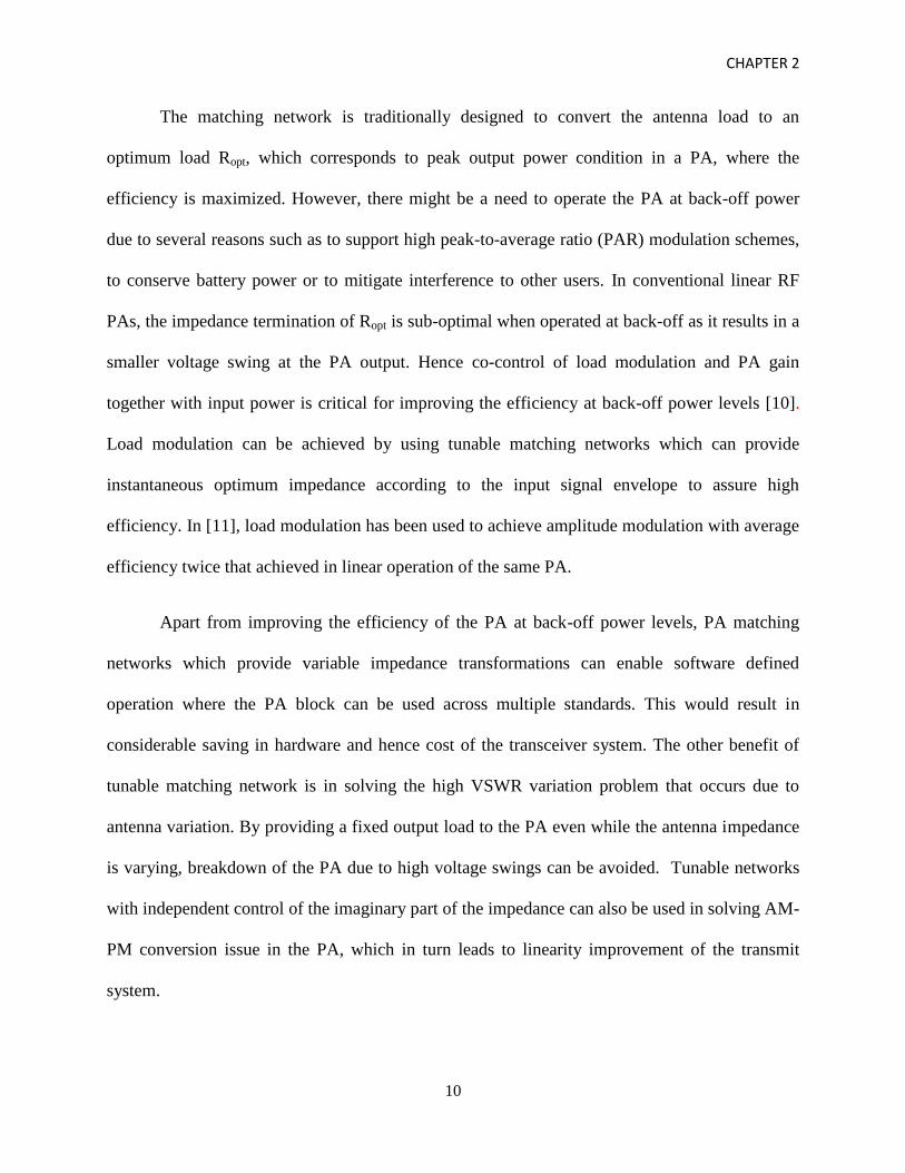
2.1 Optimal Load for a PA
Power Amplifier is the most power hungry block in wireless transmitters and its
efficiency dictates the efficiency of the entire transmitter [8]. Therefore, in order to extract the
required output power from the power amplifier while operating at its best efficiency, both
voltage and current swings need to be maximized at the PA output. In order to understand the
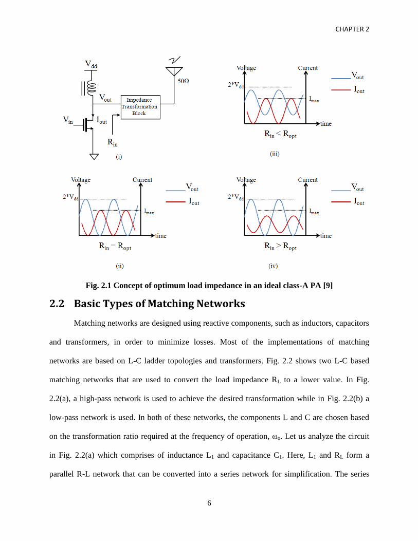
concept of optimal load, let us consider a linear power amplifier. Fig. 2.1(i) shows a power
amplifier operating in class-A mode. The maximum current that can be obtained from this PA
depends on the sizing of the NMOS transistor. Let us assume that the NMOS transistor has been
sized to give a maximum drain current of ‘Imax’ at a particular input drive voltage, ‘Vin’.
Assuming that the Vdsat for the NMOS transistor is 0V, the maximum peak-to-peak output
CHAPTER 2
5
voltage swing that can be obtained at the drain of NMOS is 2*Vdd (Practically Vdsat>0V and the
maximum Vout, while maintaining the transistor in saturation, thus will be 2*(Vdd-Vdsat)).
However, to get this maximum voltage swing under the maximum current output condition of
Iout=Imax, the impedance at the output of the PA needs to be set to the right value. This is defined
as the optimum impedance, Ropt, for the PA. When the impedance at PA output (here, at the drain
of the NMOS) is Ropt, then both voltage and current swings are maximized resulting in maximum
output power, as shown in Fig. 2.1(ii). The antenna impedance is typically 50Ω and there needs
to be an impedance transformation network which converts the antenna impedance to an
optimum value at the PA output (Fig. 2.1(i)). If the impedance presented to the PA is lower than
Ropt (Rin<Ropt), the voltage swing is not rail-to-rail and hence the power delivered decreases. This
is shown in Fig. 2.1(iii) where Vout is less than 2*Vdd. On the other hand, if the impedance
presented is too large (Rin>Ropt), there will be clipping of the output voltage which results in
reduced power in the fundamental frequency and increased harmonics. To avoid clipping the
driver might need to be backed-off, in which case, the current swing Iout<Imax. This is shown in
Fig. 2.1(iv). This implies that depending on the value of the load-resistance, either the output
voltage or the output current might be sub-optimal unless the terminating resistance is equal to
Ropt.
Load pull simulations are done on a PA to establish the value of this optimum impedance
during the design of the PA. Depending on the Ropt value, a suitable impedance transformation
block is designed to convert the 50Ω impedance of the antenna to Ropt at the PA output. In the
next section some of the basic types of matching networks are discussed.
CHAPTER 2
6
Fig. 2.1 Concept of optimum load impedance in an ideal class-A PA [9]
2.2 Basic Types of Matching Networks
Matching networks are designed using reactive components, such as inductors, capacitors
and transformers, in order to minimize losses. Most of the implementations of matching
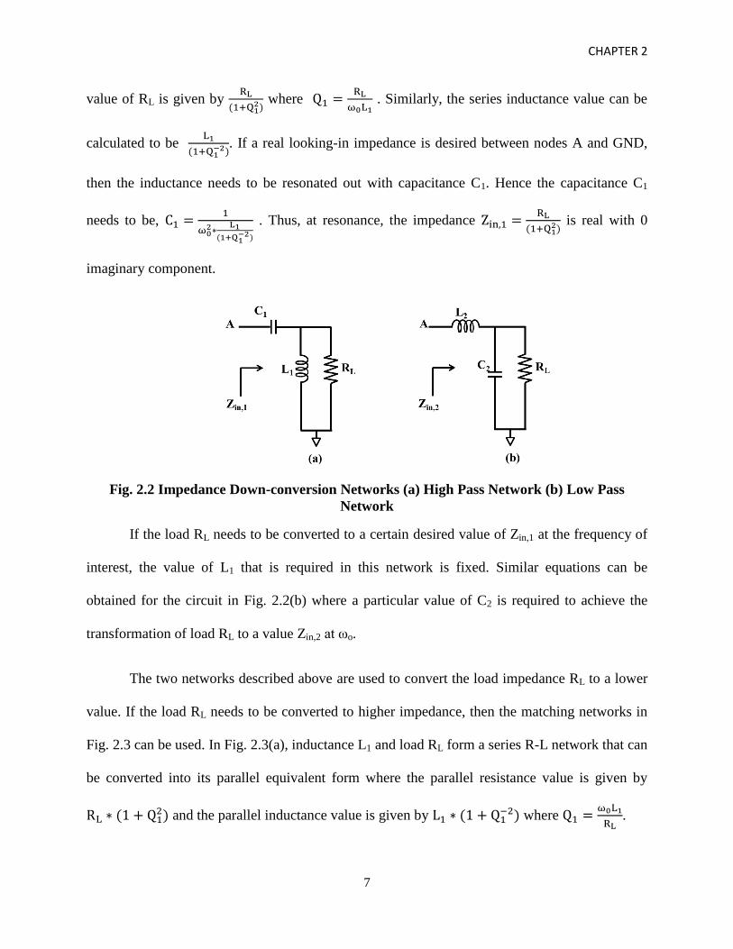
networks are based on L-C ladder topologies and transformers. Fig. 2.2 shows two L-C based
matching networks that are used to convert the load impedance RL to a lower value. In Fig.
2.2(a), a high-pass network is used to achieve the desired transformation while in Fig. 2.2(b) a
low-pass network is used. In both of these networks, the components L and C are chosen based
on the transformation ratio required at the frequency of operation, ωo. Let us analyze the circuit
in Fig. 2.2(a) which comprises of inductance L1 and capacitance C1. Here, L1 and RL form a
parallel R-L network that can be converted into a series network for simplification. The series
CHAPTER 2
7
value of RL is given by
( )
where
. Similarly, the series inductance value can be
calculated to be
( )
. If a real looking-in impedance is desired between nodes A and GND,
then the inductance needs to be resonated out with capacitance C1. Hence the capacitance C1
needs to be,
( )
. Thus, at resonance, the impedance
( )
is real with 0
imaginary component.
Fig. 2.2 Impedance Down-conversion Networks (a) High Pass Network (b) Low Pass
Network
If the load RL needs to be converted to a certain desired value of Zin,1 at the frequency of
interest, the value of L1 that is required in this network is fixed. Similar equations can be
obtained for the circuit in Fig. 2.2(b) where a particular value of C2 is required to achieve the
transformation of load RL to a value Zin,2 at ωo.
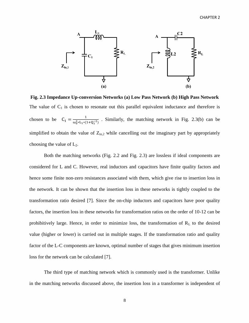
The two networks described above are used to convert the load impedance RL to a lower
value. If the load RL needs to be converted to higher impedance, then the matching networks in
Fig. 2.3 can be used. In Fig. 2.3(a), inductance L1 and load RL form a series R-L network that can
be converted into its parallel equivalent form where the parallel resistance value is given by
( ) and the parallel inductance value is given by (
) where
.
CHAPTER 2
8
Fig. 2.3 Impedance Up-conversion Networks (a) Low Pass Network (b) High Pass Network
The value of C1 is chosen to resonate out this parallel equivalent inductance and therefore is
chosen to be
(
) . Similarly, the matching network in Fig. 2.3(b) can be
simplified to obtain the value of Zin,2 while cancelling out the imaginary part by appropriately
choosing the value of L2.
Both the matching networks (Fig. 2.2 and Fig. 2.3) are lossless if ideal components are
considered for L and C. However, real inductors and capacitors have finite quality factors and
hence some finite non-zero resistances associated with them, which give rise to insertion loss in
the network. It can be shown that the insertion loss in these networks is tightly coupled to the
transformation ratio desired [7]. Since the on-chip inductors and capacitors have poor quality
factors, the insertion loss in these networks for transformation ratios on the order of 10-12 can be
prohibitively large. Hence, in order to minimize loss, the transformation of RL to the desired
value (higher or lower) is carried out in multiple stages. If the transformation ratio and quality
factor of the L-C components are known, optimal number of stages that gives minimum insertion
loss for the network can be calculated [7].
The third type of matching network which is commonly used is the transformer. Unlike
in the matching networks discussed above, the insertion loss in a transformer is independent of
CHAPTER 2
9
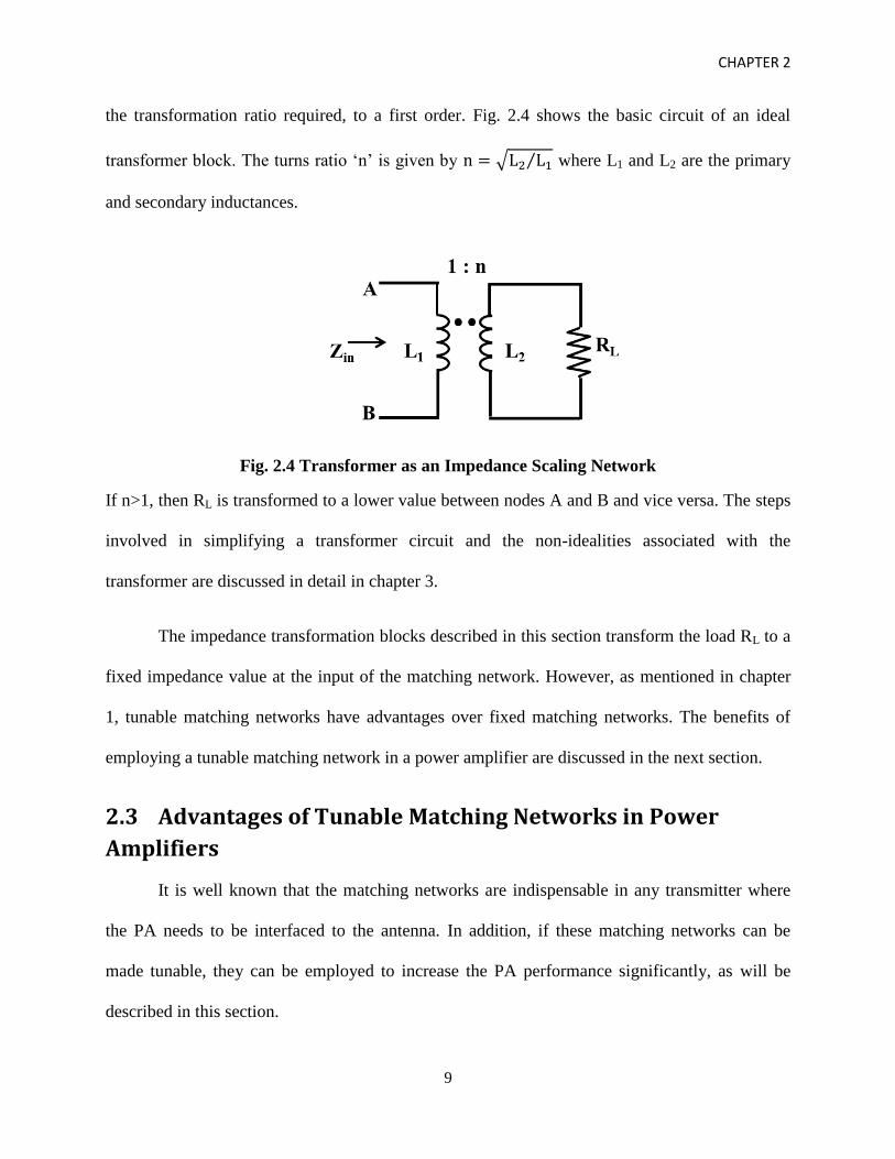
the transformation ratio required, to a first order. Fig. 2.4 shows the basic circuit of an ideal
transformer block. The turns ratio ‘n’ is given by √ ⁄ where L1 and L2 are the primary
and secondary inductances.
Fig. 2.4 Transformer as an Impedance Scaling Network
If n>1, then RL is transformed to a lower value between nodes A and B and vice versa. The steps
involved in simplifying a transformer circuit and the non-idealities associated with the
transformer are discussed in detail in chapter 3.
The impedance transformation blocks described in this section transform the load RL to a
fixed impedance value at the input of the matching network. However, as mentioned in chapter
1, tunable matching networks have advantages over fixed matching networks. The benefits of
employing a tunable matching network in a power amplifier are discussed in the next section.
2.3 Advantages of Tunable Matching Networks in Power
Amplifiers
It is well known that the matching networks are indispensable in any transmitter where
the PA needs to be interfaced to the antenna. In addition, if these matching networks can be
made tunable, they can be employed to increase the PA performance significantly, as will be
described in this section.
CHAPTER 2
10
The matching network is traditionally designed to convert the antenna load to an
optimum load Ropt, which corresponds to peak output power condition in a PA, where the
efficiency is maximized. However, there might be a need to operate the PA at back-off power
due to several reasons such as to support high peak-to-average ratio (PAR) modulation schemes,
to conserve battery power or to mitigate interference to other users. In conventional linear RF
PAs, the impedance termination of Ropt is sub-optimal when operated at back-off as it results in a
smaller voltage swing at the PA output. Hence co-control of load modulation and PA gain
together with input power is critical for improving the efficiency at back-off power levels [10].
Load modulation can be achieved by using tunable matching networks which can provide
instantaneous optimum impedance according to the input signal envelope to assure high
efficiency. In [11], load modulation has been used to achieve amplitude modulation with average
efficiency twice that achieved in linear operation of the same PA.
Apart from improving the efficiency of the PA at back-off power levels, PA matching
networks which provide variable impedance transformations can enable software defined
operation where the PA block can be used across multiple standards. This would result in
considerable saving in hardware and hence cost of the transceiver system. The other benefit of
tunable matching network is in solving the high VSWR variation problem that occurs due to
antenna variation. By providing a fixed output load to the PA even while the antenna impedance
is varying, breakdown of the PA due to high voltage swings can be avoided. Tunable networks
with independent control of the imaginary part of the impedance can also be used in solving AM-
PM conversion issue in the PA, which in turn leads to linearity improvement of the transmit
system.

CHAPTER 2
11
In the next two sub-sections two of the benefits of tunable networks that were mentioned
in this part will be explained in more detail.
2.3.1 Power Requirements and Ropt values in different standards
To get an understanding about the range of impedances that is required from the output
matching network, consider a transmitter designed to operate over two commercial standards:
Bluetooth (BT) and Wi-Fi, both of which operate in the unlicensed 2.4GHz ISM band. For a
class-1 Bluetooth transmitter, the maximum power that can be radiated from the transmitter is
20dBm [12]. Therefore, let us consider a system which requires a BT transmitter with 20dBm
output power, working off a 1.8V supply. For an ideal PA-stage, with no voltage drop across the
switch in the final stage, the maximum voltage swing possible at this supply is 2*1.8V (peak-to-
peak). Therefore, to obtain 20dBm output power while maintaining peak voltage swing possible
at PA output, the resistance at the output of the PA needs to be 16Ω. If the same system needs to
support Wi-Fi standard as well, in addition to sizing the PA transistor appropriately, the Ropt that
needs to be presented to the PA needs to be modified to adapt to the desired output power. The
maximum transmitter power output in a Wi-Fi system needs to be less than 30dBm [13]. If we
need to design the PA to support 30dBm, the value of Ropt needs to be 1.6Ω for obtaining a
voltage swing of 2*1.8V (peak-to-peak) at PA output. So, in order to support both BT and Wi-Fi
standards operating at their maximum transmit capability, the PA output matching network needs
to convert a 50Ω antenna impedance to 16Ω as well as 1.6Ω. If we define tuning-range as the
ratio of the maximum to minimum transformation ratios, then, in this example, a tuning-ratio of
approximately ‘10x’ is required. This means that the tuning range requirement of the matching
network is 10. Now if the BT transmitter needs to output lesser than 20dBm power, then the Ropt
CHAPTER 2
12
value increases further from 16Ω placing a much higher tuning range requirement. Hence, it is
necessary to have a matching network which can support a wide tuning range.
2.3.2 AM-PM Conversion in Power Amplifiers
As mentioned in section 2.1, the matching network that interfaces the PA to the antenna
provides Ropt at PA output for maximum power output from the PA. In addition to this, the
matching network also needs to absorb the drain capacitance on the PA output node in order to
operate at GHz frequencies. The matching network is usually designed for a fixed drain
capacitance on the PA output node, which is assumed to remain constant irrespective of the
output power level. However, this is not the case. In addition to variation in the non-linear drain
capacitance, there are several other factors that cause non-linearity in the PA stage, which cause
an output signal phase dependence on the amplitude of the PA output signal. This leads to AM-
PM distortion in PAs. AM-PM distortion in PAs used in communication systems, which are
based on modulation schemes like FM, QPSK, QAM, can result in an increased Error-Vector-
Magnitude (EVM) and hence increased Bit-Error-Rates (BER).
Different methods have been adopted in systems to solve the AM-PM distortion problem.
Pre-distortion algorithms are used where the AM-PM distortion in the PA is corrected for by
adding additional phase shift at the input of the PA, thus increasing the linearity of the PA [30].
Another method to reduce the effect of AM-PM distortion is through the use of a tunable
matching network. By monitoring the input power level to the PA and adjusting the Ropt to the
PA such that a fixed voltage swing results at the PA output, the non-linearity associated with the
drain capacitance of the PA can be eliminated. The PM distortion that arises due to capacitance
variation at the PA input and due to other non-linearities in the PA output stage can be
compensated for by providing a variable imaginary part at the PA output along with variable real
CHAPTER 2
13
impedance. However, this would require the matching network’s tuning bandwidth to be
relatively higher as compared to the baseband signal that carries information.
Thus, it is clear that having tunability in matching networks which are employed at the
output of the PA can prove to be very beneficial and improve the PA performance significantly.
However, there are several challenges involved in building tunable matching networks in Silicon
bulk-CMOS process as will be discussed in the next section.
2.4 Challenges in Tunable Matching Network Design
Matching networks are designed using reactive components, such as inductors and
capacitors as there are ideally lossless. However, the reactive components that are realized on-
chip have finite, low quality factors making them prone to losses. This problem of loss in the
matching network is further exacerbated at lower technology nodes due to the increasing
demands of the system from the matching network. For example, scaling of supply voltage at
smaller process nodes requires that the Ropt be small at the PA output in order to extract large
output powers. This might demand a transformation ratio of the order of 10-12 from the PA
output matching network. The design of the matching network for such high transformation
ratios becomes more challenging and the insertion loss in them increases [7]. At low frequencies,
the quality factor of inductors is dependent on the resistivity of the metal used in building the
inductor while at higher frequencies the amount of substrate loss due to magnetic and capacitive
coupling to substrate dictates the maximum quality factor attainable. The quality factor of on-
chip capacitors is better than inductors when the frequency of operation is in few GHz. Hence, in
order to build low-loss networks, high quality factor inductors need to be designed. One way to
build better inductors is by using low-resistivity metal layers which are at a larger distance from
the substrate. If the frequency of operation is slightly higher than 10’s of GHz, then a pattern
CHAPTER 2
14
ground shield can be added around the inductor, which can help improve the performance. While
it is challenging to design matching networks with good performance on-chip, introducing the
element of tunability makes the problem even harder to solve.
Tuning in matching networks can be achieved by either varying the inductors or the
capacitors. Multi-tap inductors [17], multi-tap inductors along with switch-capacitors [18], [19]
and magnetically-tuned transformers [20] have been considered in some of the prior publications
to implement tunability while others have used capacitor as the tuning element [14]. If capacitor
is used as the tuning element, variable capacitance can be obtained by using either varactors or
switch-capacitor banks. Though varactors can provide continuous tuning, the change in the
capacitance value due to signal variation at the varactor leads to AM-PM distortion [21]. Special
techniques need to be incorporated both while manufacturing the varactors and designing the
networks with varactors in order to eliminate AM-PM distortion [22]. While these techniques
solve the problem of distortion and non-linearity, they eliminate the goal of realizing a single
CMOS chip for the entire transceiver block. Tuning the capacitors using switches does not pose
linearity problems as severe as the varactors. However, the switches, due to their non-zero
resistance, can cause considerable increase in the insertion loss in the system. This has the effect
of degrading the capacitor Q, and becomes more problematic at higher frequencies. In addition to
loss, switches also introduce considerable amount of parasitics which will limit the tuning range.
Hence, if switches are used for tuning, the choice of inductor or capacitor as the tuning element
depends on the impact of the switch resistance on the overall loss and tuning range in the
network.
Most of the implementations of tunable matching networks for PA-antenna interface are
based on LC ladder topologies, T-network, Pi-network, etc. While some of them are fabricated in
CHAPTER 2
15
high voltage silicon-on-insulator processes and make use of varactors for obtaining tuning [14],
the others make use of off-chip components to realize the matching network [15], [16]. Though
better performance can be obtained by using off-chip components and high-voltage varactors in
better processes, the goal of realizing the entire system on a single-chip is eliminated. With the
objective of integrating the entire matching network in bulk-CMOS processes, in this work,
switch-capacitor banks along with on-chip transformers, inductors and capacitors have been used
to obtain the required tuning in the matching network. Unlike in implementations that need large
control voltages to operate the switches or tune the varactors, the switches in this design operate
off a 1V control voltage.
CHAPTER 3
16
3. Transformer-Based Matching Networks
Matching networks which are desired to operate in a given frequency band can be
designed using transformers or LC ladders. While LC-ladder based circuits such as a T-network,
Pi-network, or a combination of these are well suited for low transformation ratios, their
insertion loss is prohibitively high for transformation ratios on the order of 10-12 [7], [23].
Transformers, on the other hand, are ideally suited for such applications because the insertion
loss is independent of the transformation ratio [24]. In addition to the above mentioned
advantage, transformer-based networks serve other purposes, including as a balun, to interface a
differential PA with a single-ended antenna. In addition, it can also eliminate the necessity of a
large choke inductor by utilizing the center-tap of the transformer to deliver a bias to the PA
input or output.
For high-power PAs using transformer-based matching networks, the overall system
power-efficiency will be dependent on the insertion-loss of the transformer. Hence, in this
chapter, criteria for designing transformer networks are developed with the goal of minimizing
insertion loss. The assumption made for developing optimum design guidelines is that the
primary and secondary inductance values in the transformer are chosen based on the impedance
transformation ratio requirement and are fixed in value. The optimization is in terms of the
selection of a secondary capacitor value for the given transformer such that the insertion loss of
the loaded transformer network is at its minimum. Section 3.1 describes the modeling of the
transformer. In section 3.2, a methodology for simplification of the transformer network is
presented and equations for insertion loss are derived. Based on these, the selection criteria for
secondary capacitance are obtained. The validation of the methodology developed in section 3.2
CHAPTER 3
17
is presented in section 3.3, while section 3.4 compares and contrasts the use of a parallel vs.
series secondary capacitors in the transformer-based matching network design.
3.1 Transformer model
Transformers can be modeled using pi-models, similar to inductors. Fig. 3.1 shows the
transformer model which accommodates the center-tap connection and distributed capacitance
effects at high frequencies. Cp and Cs are terminal-to-substrate capacitances, Rb is the pattern
ground shield parasitic resistance, Cc is the terminal-to-terminal capacitance and Rp, Rs are the
equivalent series resistances on the primary and secondary terminals which capture the ohmic
losses, skin effect and proximity effects. Lp and Ls are the primary and secondary inductances
and the coupling co-efficient between primary and secondary is given by ‘km’.
Fig. 3.1 Frequency-dependent lumped element model for transformer [25]
If the frequency of operation is much lower than the self- resonance frequencies of primary and
secondary inductances, then for the sake of simplicity, the model can be approximated as shown
CHAPTER 3
18
in Fig. 3.2 (the center-tap becomes important for common-mode analysis and can be ignored
while considering differential operation of the circuit).
Since on-chip transformers and inductors implemented using the metal-stacks available in
standard CMOS technology have lower quality factor than discrete off-chip components, the
values of Rp and Rs could be quite high. This is primarily due to the power loss due to the finite
resistance of the metal windings, in addition to the lossy substrate [26]. In advanced technology
nodes such as 28 and 40nm, this problem is even more pronounced because of the shrinking
height of the metal stack through technology scaling. Hence, it is essential to design the
transformer network carefully such that the losses due to high Rp and Rs are reduced. Else, the
insertion loss of the matching network could be quite high which in turn will reduce the overall
efficiency of the system where the matching network is employed. In the next section, the choice
of the secondary capacitor for obtaining minimum insertion loss is discussed at length using the
transformer model described above.
Fig. 3.2 Low frequency approximation of broadband model for transformer
CHAPTER 3
19
3.2 Transformer matching network design to minimize
insertion loss
Matching network design requirements can be quite different depending on the
application. For example, the matching network used at the receiver front-end for LNA matching
needs to be optimized for low noise, good matching with antenna impedance and voltage gain.
For VCO applications, the matching network needs to have good phase noise and narrow-
bandwidth implying a high Q. For a PA matching network, impedance transformation with
minimum loss in the network is of utmost importance. Hence, in this section, design of
transformer-based matching network which provides minimum insertion loss is discussed.
Loss in matching networks can be characterized in different ways. While one way is to
calculate loss which is independent of the source impedance and the termination load impedance,
the other method is to characterize the loss of the entire network (which includes the source and
load resistance). In some publications, the maximum available gain, Gmax, is used as a figure-of-
merit to characterize the loss since it is independent of the termination impedances. (Gmax, in a
transformer, corresponds to the power transfer from the primary coil to the secondary coil under
bilateral conjugate matched conditions) In [27], Gmax of the transformer is derived and ways to
improve the Gmax are discussed. However, in applications where transfer of power is the primary
objective, it makes more sense to characterize the network insertion loss (for given termination
source/load impedances) since it helps in estimating the actual power delivered to the load in
presence of the matching network. Based on this, insertion loss (IL) of an impedance matching
network can be defined as –
(
)
CHAPTER 3
20
where Pload is the power delivered to the load and Ploss is the power dissipated in the matching
network. Note that the matching network’s insertion loss is dependent on the value of load
impedance and changes when the load is changed. In this section, the criteria for choosing a
secondary capacitor for a given transformer, in a transformer-based matching network, are
described. Equations for insertion loss in the transformer-matching network are also provided.
Fig. 3.3 Non-ideal transformer with turns ratio ‘n’
Consider the transformer shown in Fig. 3.3. The terminals (A, B) represent the primary
side of the transformer and terminals (C, D) represent the secondary side. L1 and L2 are the
primary and secondary inductances, respectively. The turns-ratio of the transformer denoted as
‘n’ is defined as √ ⁄ and the magnetic coupling-coefficient is denoted as km. R1 and R2
are the equivalent series resistances on the primary and secondary windings. The insertion loss in
the network arises due to these resistances and hence they need to be minimized. The quality
factor (Q-factor) of primary and secondary windings, Q1 and Q2, are defined as
⁄
and
⁄ respectively. Theoretically, there are two equivalent techniques to model the
Q-factor of an inductor: first, with a series resistance , where ⁄ , and second, with a
parallel resistance , where . However, it is important to note that representing the
CHAPTER 3
21
inductor and the series equivalent resistor in their parallel equivalent form will lead to inaccurate
results in a transformer. In section 3.3 the incorrect conclusion drawn by assuming the parallel-
resistance model will be highlighted.
If the transformer described above is terminated with a resistance RL at the secondary, the
input impedance at the primary can be obtained by simplifying to a form shown in Fig. 3.4(b).
Non-ideal magnetic coupling between L1 and L2 results in a leakage inductance which has been
accounted for on the primary side, whose value is ( ) [28]. The impedance at the
secondary, which consists of in parallel with ( ) is reflected on the primary with a
scaling-factor of ( ⁄ ) which is the effective turns-ratio [28]. The reflected impedance
appears in series with the primary leakage inductance, ( ) and primary ESR, .
Fig. 3.4 Equivalent circuit of a loaded transformer with impedances reflected onto primary
side
Fig. 3.4(b) is the simplest representation of a transformer and helps in accurately evaluating the
looking-in impedance, Zin, as seen from the primary of the transformer. It can be observed from
this model that impedance Zin has both resistive and inductive components. However, in most
applications, it is desirable for the transformer to be ‘tuned’ to ensure the input-impedance is real
in the frequency range of interest. Shunt/series capacitances can be added at the
CHAPTER 3
22
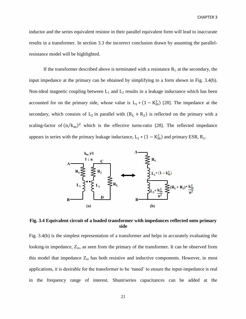
primary/secondary terminals to resonate the inductance. Out of these four cases, it can be shown
that the shunt-capacitance at the secondary is the most generic case. In this section,
simplification of the transformer network is discussed, which will provide an intuition for the
impact of tuning-capacitance on the insertion-loss.
Fig. 3.5 Steps involved in simplifying a transformer with parallel secondary capacitor and
load RL
The transformer-model with the secondary tuning capacitance is shown in Fig. 3.5(a).
The secondary capacitor C2 and RL form a parallel R-C network. At the center frequency ω0, the
CHAPTER 3
23
parallel-circuit can be transformed to its narrowband equivalent series network, in series
with , as shown in Fig. 3.5(a) and (b), where
( )
(1a)
(
) (1b)
(1c)
The resistance and form a voltage divider network. As a result, in order to
minimize the losses needs to be large compared to . From (1a)-(1c), one observes that
is maximized by minimizing and . Thus, a low value of suppresses the contribution of
to the total insertion-loss. Next, to study the impact of on the insertion loss caused due to
primary side loss-resistance , the circuit transformations described in Fig. 3.5(c-g) are
discussed.
The series network consisting of C2’ and (RL’+R2) can be transformed to an equivalent
parallel network as shown in Fig. 3.5(c) and (d) with
( )
( ) (
) (2a)
( )
(2b)
(
)
(2c)
The effective shunt-capacitance resonates with a part of L2 at ω0. Inductance L2 can be
represented as a parallel combination of two inductors, say L2’ and L2”, such that L2” and C2”
satisfy (3a). The residual inductance L2’ is then given by eqn. (3b)
CHAPTER 3
24
(3a)
(3b)
Next, as shown in Fig. 3.5(f), the secondary impedance, L2’ in parallel with (RL’+R2)”, is
referred from the secondary to the primary of the transformer. As a result the impedances are
scaled down by a factor of ( ⁄ ) . On the primary side, the parallel to series conversion of
L2’*( ⁄ ) and (RL’+R2)”*(
⁄ ) gives Leff and Reff, as indicated in Fig. 3.5(g). Resistance
Reff represents the loading on the primary of the transformer and can be obtained using (4a) and
(4b).
(
)
(4a)
( )
⁄
( )
(4b)
Reff can be split as RL,eff and R2,eff as given in equations (5a) and (5b). RL,eff represents the load
resistor and R2,eff represents the ESR R2 when referred to the primary side.
(
)
⁄
( )
(5a)
( )
⁄
( )
(5b)
CHAPTER 3
25
In order to minimize insertion loss, the value of RL,eff needs to be much larger as compared to the
two loss components, R2,eff and R1. Since all three resistances appear in series, to minimize the
IL, the factor M must be maximized, where
(6)
Several important observations can be made based on (6). First, if C2 is minimized, from
(1a)-(1c) it can be seen that is maximized. However for small values of C2, RL,eff also reduces
thus increasing the loss due to R1. In summary, there exists an optimum value of C2 for which the
ratio M is maximized i.e. loss due to both R1 & R2 are minimized. This optimum value of C2
gives the least insertion loss for a given transformer. The insertion loss can be calculated using
(7).
[
]
(7)
The above criterion has been used in selecting the secondary capacitor C2 in the design of tuning
networks in chapter 4.
3.3 Validation of the transformer-matching network model
An example validating the model given in the previous section and conditions for
choosing C2 are described below. A transformer with turns-ratio 1:2 and a primary inductance of
approximately 400pH were chosen to construct the transformer matching network. The exact
values of primary and secondary inductances were obtained from HFSS simulations of the
transformer that was laid out in a 40nm CMOS process. These values were found to be
L1=324pH and L2=2.7nH. The value of ESRs on primary and secondary windings were obtained
CHAPTER 3
26
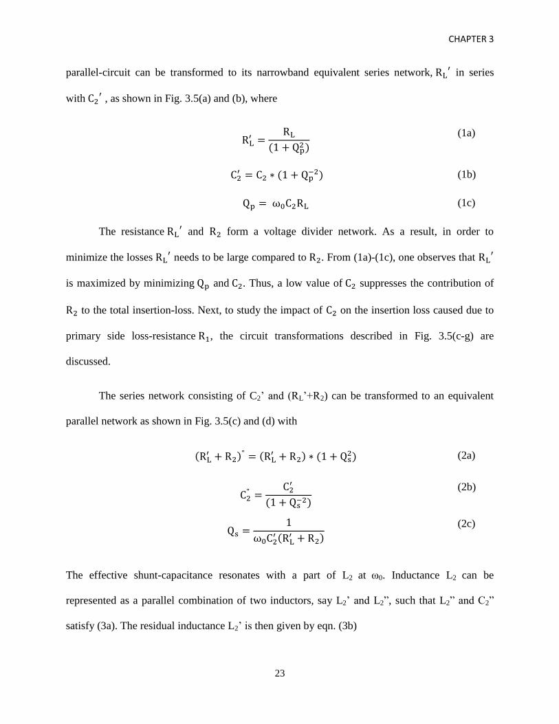
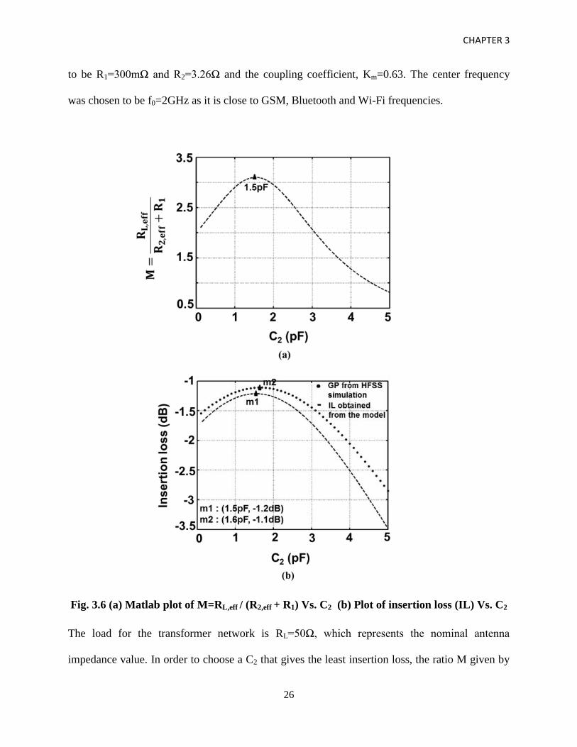
to be R1=300mΩ and R2=3.26Ω and the coupling coefficient, Km=0.63. The center frequency
was chosen to be f0=2GHz as it is close to GSM, Bluetooth and Wi-Fi frequencies.
Fig. 3.6 (a) Matlab plot of M=RL,eff / (R2,eff + R1) Vs. C2 (b) Plot of insertion loss (IL) Vs. C2
The load for the transformer network is RL=50Ω, which represents the nominal antenna
impedance value. In order to choose a C2 that gives the least insertion loss, the ratio M given by
CHAPTER 3
27
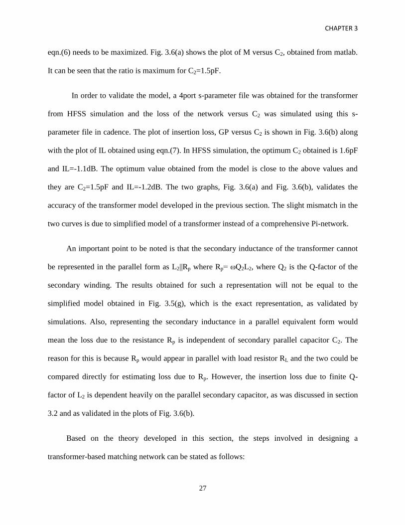
eqn.(6) needs to be maximized. Fig. 3.6(a) shows the plot of M versus C2, obtained from matlab.
It can be seen that the ratio is maximum for C2=1.5pF.
In order to validate the model, a 4port s-parameter file was obtained for the transformer
from HFSS simulation and the loss of the network versus C2 was simulated using this s-
parameter file in cadence. The plot of insertion loss, GP versus C2 is shown in Fig. 3.6(b) along
with the plot of IL obtained using eqn.(7). In HFSS simulation, the optimum C2 obtained is 1.6pF
and IL=-1.1dB. The optimum value obtained from the model is close to the above values and
they are C2=1.5pF and IL=-1.2dB. The two graphs, Fig. 3.6(a) and Fig. 3.6(b), validates the
accuracy of the transformer model developed in the previous section. The slight mismatch in the
two curves is due to simplified model of a transformer instead of a comprehensive Pi-network.
An important point to be noted is that the secondary inductance of the transformer cannot
be represented in the parallel form as L2||Rp where Rp= ωQ2L2, where Q2 is the Q-factor of the
secondary winding. The results obtained for such a representation will not be equal to the
simplified model obtained in Fig. 3.5(g), which is the exact representation, as validated by
simulations. Also, representing the secondary inductance in a parallel equivalent form would
mean the loss due to the resistance Rp is independent of secondary parallel capacitor C2. The
reason for this is because Rp would appear in parallel with load resistor RL and the two could be
compared directly for estimating loss due to Rp. However, the insertion loss due to finite Q-
factor of L2 is dependent heavily on the parallel secondary capacitor, as was discussed in section
3.2 and as validated in the plots of Fig. 3.6(b).
Based on the theory developed in this section, the steps involved in designing a
transformer-based matching network can be stated as follows:

CHAPTER 3
28
1. Determine the turns-ratio required to achieve the required transformation ratio
2. Choose L1 and L2 values which meet the turns-ratio specification based on the area and
SRF (self-resonance frequency) constraint
3. Layout the transformer such that the Q-factor in the primary and secondary windings are
maximized
4. Once the transformer layout is ready, select the value of secondary capacitor based on the
criteria mentioned in the above section in order to obtain least insertion loss.
It is important to note that the primary capacitance does not play any role in determining
the insertion loss in the network (unless the transformation requires a very large Rin, where the
quality factor of the on-chip capacitor might add to the insertion loss) and hence is chosen solely
based on the residual inductance in the matching network that needs to be resonated.
3.4 Parallel secondary capacitor vs. Series secondary
capacitor
In section 3.2, the insertion loss equation was derived based on the assumption that the
secondary capacitor is in parallel with the load RL. However, the set of equations described in 3.2
hold true even for a series secondary capacitor. The starting step for such a configuration would
be Fig. 3.5(b). The rest of the steps remain the same. The choice of series secondary capacitor
versus a parallel secondary capacitor depends on the application of the system where the
matching network is employed. If a series secondary capacitor is chosen, since the value of
secondary winding’s ESR R2 compares directly with RL (as can be seen in Fig. 3.5(b)), the loss
due to R2 remains constant irrespective of the value of series capacitor C2 chosen. Hence the
value of C2 can be chosen so as to minimize the loss that arises due to the primary winding’s
ESR R1. In configurations which have parallel secondary capacitors, the value of C2 cannot be
CHAPTER 3
29
made too large or too small as it would increase the loss in either R2 or R1 respectively. This
places a trade-off constraint on the selection of C2. However, in configurations which have series
secondary capacitors, since the loss in R2 is independent of C2, the value of C2 can be chosen to
minimize the loss in R1. This helps to make the insertion loss minimal over wide band of
frequencies in a series-secondary capacitor configuration. Therefore, in applications where
insertion loss needs to be made minimum over wide band of frequencies, series-secondary
capacitors are preferred. On the other hand, if the application requires the matching network to
be narrow-band so as to reject out-of-band signals, then parallel-secondary-capacitor
configurations are preferred.
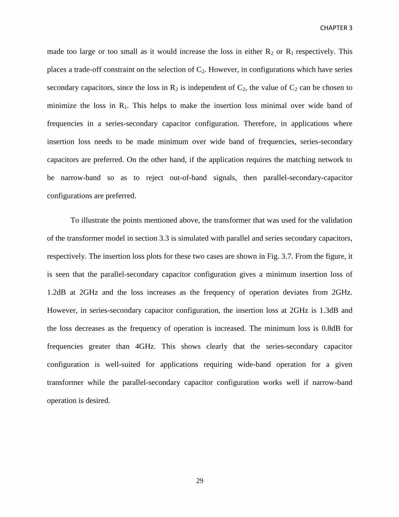
To illustrate the points mentioned above, the transformer that was used for the validation
of the transformer model in section 3.3 is simulated with parallel and series secondary capacitors,
respectively. The insertion loss plots for these two cases are shown in Fig. 3.7. From the figure, it
is seen that the parallel-secondary capacitor configuration gives a minimum insertion loss of
1.2dB at 2GHz and the loss increases as the frequency of operation deviates from 2GHz.
However, in series-secondary capacitor configuration, the insertion loss at 2GHz is 1.3dB and
the loss decreases as the frequency of operation is increased. The minimum loss is 0.8dB for
frequencies greater than 4GHz. This shows clearly that the series-secondary capacitor
configuration is well-suited for applications requiring wide-band operation for a given
transformer while the parallel-secondary capacitor configuration works well if narrow-band
operation is desired.
CHAPTER 3
30
Fig. 3.7 Plot of insertion loss Vs. freq. in a transformer with series/parallel secondary
capacitors
CHAPTER 4
31
4. Tunable Matching Network Design
In order to fulfill the multi-standard and multi-mode demands of the ever-growing mobile
device market (cellphones, laptops, tablets), current implementations contain an array of on-
board duplexers and matching networks to interface the antenna with multiple RFIC transceiver
chips. The goal of eliminating multiple off-chip matching networks, while supporting multi-
standard communication provides a huge motivation to build fully-integrated tunable matching
networks.
Two key parameters which characterize matching networks at the chip-boundaries are the
impedance transformation-ratio (N), and the resonant frequency (ωR) at which the transformation
ratio N is valid. Furthermore, this leads us to identify two forms of tunability: frequency-
tunability, and impedance-tunability. In this chapter, the design of a fixed-frequency, impedance-
tunable matching network is described.
Traditionally, the matching network is optimized for low-insertion loss at a fixed ωR, and
a fixed transformation-ratio, N. Therefore, any tunability-algorithm must account for the
variation in insertion-loss across the tuning range. This makes tuning network design which aims
at achieving wide tuning ratios, on the order of 1:5 or 1:10, quite challenging. In chapter 3, the
advantage of a transformer-based approach for the design of a large impedance transformation-
ratio matching network was described. Extending on that foundation, two tunable matching
networks have been realized using transformers along with L- and Pi-matched circuits,
respectively. The transformer in the tunable networks steps-down the 50Ω antenna impedance to
CHAPTER 4
32
a fixed lower value and the L-or Pi-matched network converts this fixed value impedance
resulting from the transformer to variable input impedance.
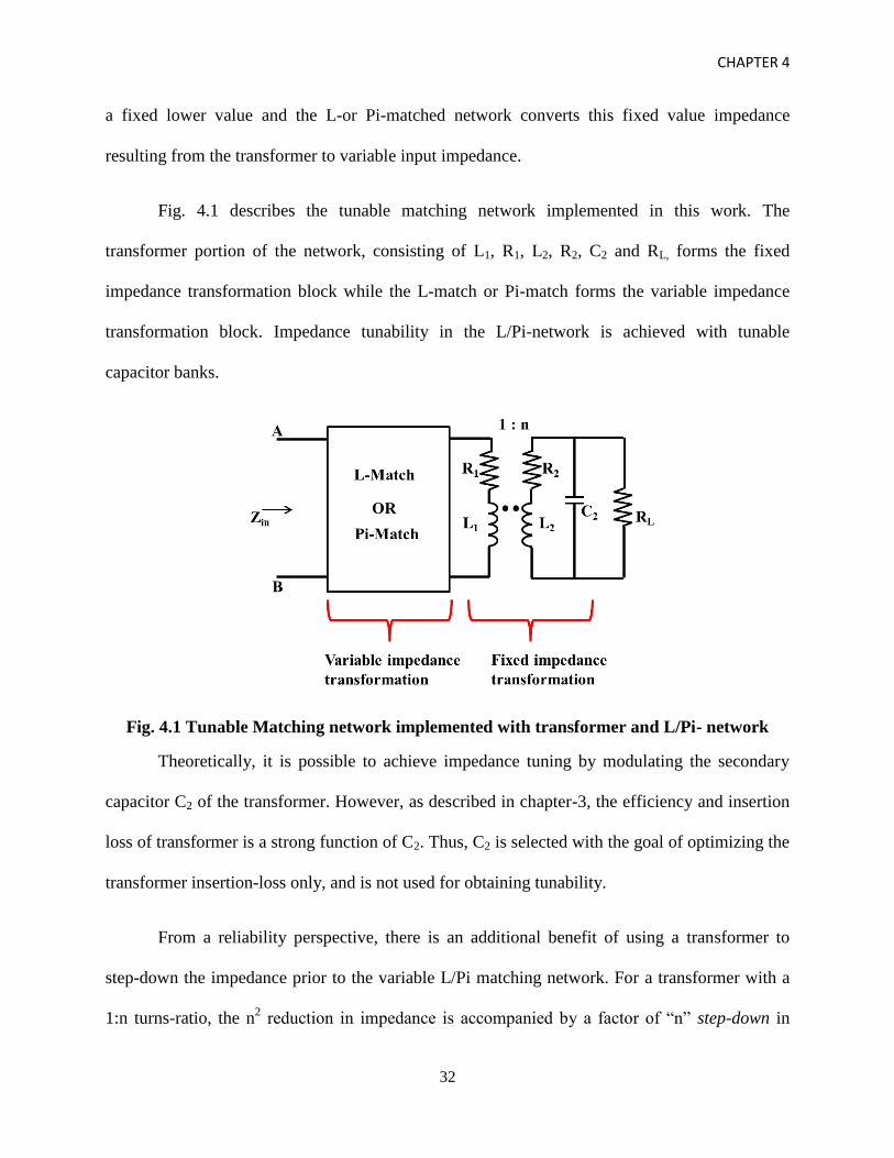
Fig. 4.1 describes the tunable matching network implemented in this work. The
transformer portion of the network, consisting of L1, R1, L2, R2, C2 and RL, forms the fixed
impedance transformation block while the L-match or Pi-match forms the variable impedance
transformation block. Impedance tunability in the L/Pi-network is achieved with tunable
capacitor banks.
Fig. 4.1 Tunable Matching network implemented with transformer and L/Pi- network
Theoretically, it is possible to achieve impedance tuning by modulating the secondary
capacitor C2 of the transformer. However, as described in chapter-3, the efficiency and insertion
loss of transformer is a strong function of C2. Thus, C2 is selected with the goal of optimizing the
transformer insertion-loss only, and is not used for obtaining tunability.
From a reliability perspective, there is an additional benefit of using a transformer to
step-down the impedance prior to the variable L/Pi matching network. For a transformer with a
1:n turns-ratio, the n2 reduction in impedance is accompanied by a factor of “n” step-down in
CHAPTER 4
33
voltage swing on the primary side as compared to the secondary. Thus, CMOS switches used in
tunable L/Pi-match sections (in the capacitor banks), are subjected to lower voltage swings
across the drain-to-gate and drain-to-bulk terminals. It is also important to note that the
capacitance C2 must sustain the same voltage swing as seen by the antenna, across its terminals.
For a PA generating 30dBm of output power, this swing could be as large as 10V. This precludes
any attempt to add a switch-capacitor bank to vary the value of C2 and obtain tunability.
The design and implementation details of the two tunable networks, transformer-plus-L-
matched network (TLMN) and transformer-plus-Pi-matched network (TPMN), are discussed in
sections 4.1 and 4.2 respectively. The two tuning networks are designed to absorb the fixed
output capacitance of the PA into the matching network, while presenting the PA with input
impedance Zin, which is real and variable. Hence, in both TLMN and TPMN, two sets of
capacitors are varied using switch-capacitor banks. While one of the capacitors tunes the real-
part of the impedance Zin, the other capacitor is necessary to maintain the imaginary part of Zin at
a constant value. In systems which need to correct the AM-PM conversion induced non-linearity,
it is possible to extend the proposed tuning structure to enable independent control over the
imaginary part of the impedance Zin as well [29], [30].
4.1 Transformer-plus-L-match-based tunable Matching
Network (TLMN)
The circuit schematic for the TLMN is shown in Fig. 4.2. The finite quality factor
transformer comprises of inductors L1, L2 and resistors R1, R2. The variable L-match is
implemented with inductor L3, and switch-capacitor banks Cvar and Cpar. The real-part of the
input impedance Zin, of the TLMN, can be varied using Cvar. The capacitor bank Cpar is used to
CHAPTER 4
34
compensate for the variation in imaginary-part of Zin, which is the resultant of a variable Cvar.
The matching network has been designed for a center frequency of 2GHz.
4.1.1 Design details
In order to demonstrate impedance tunability for large transformation ratios, the
prototype test chip is designed using a transformer with turns-ratio n≈2. A stacked-transformer
has been implemented using the ultra-thick metal layer (UTM) and Aluminum passivation layer
(AP). The transformer is characterized through a 3-D electromagnetic simulation using Ansoft’s
HFSS. The self-inductance of the primary and secondary windings of the transformer is
determined to be 362pH and 1.25nH, respectively, resulting in a transformation ratio of
approximately 1:1.86. The ESRs of primary and secondary inductances are R1=0.7Ω and
R2=1.87Ω and the coupling co-efficient, km=0.65. The secondary capacitor C2 is selected using
the minimum insertion loss criteria derived in section 3.2. At the operating frequency of 2GHz, a
secondary capacitance of 3.9pF results in a minimum insertion loss of 1.9dB.
The variable capacitors in the tunable network, Cvar and Cpar, are realized using switch-
capacitor banks as shown in Fig. 4.2. The capacitors in this network are implemented using
MOM-capacitors as these capacitors are significantly more linear than a junction-based varactor
diode, hence producing lower distortion products [31].
Ideally, ON/OFF switches in series with a capacitor, should be sized to minimize the ON
resistance and hence, the insertion loss. However, increasing the switch size to reduce the ON
resistance will result in increased parasitic capacitances associated with the switch. The parasitic
capacitances of the switch will constrain the minimum Cvar and Cpar values that can be realized,
which in turn will limit the tuning range.
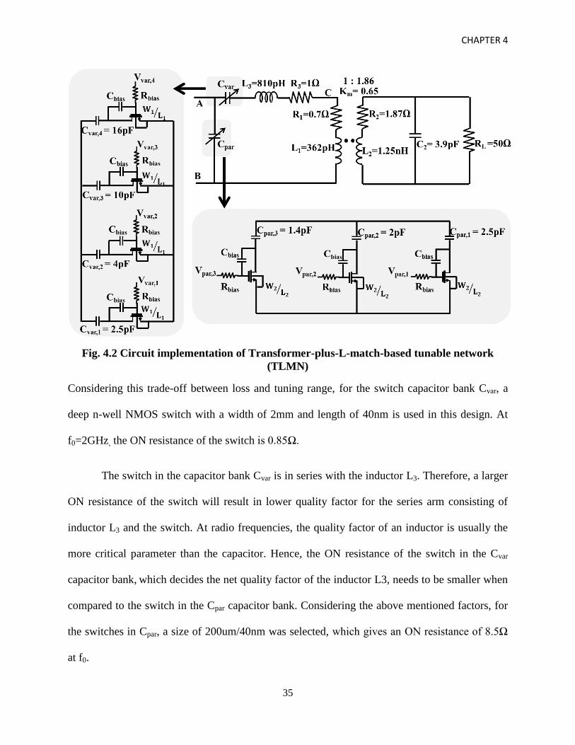
CHAPTER 4
35
Fig. 4.2 Circuit implementation of Transformer-plus-L-match-based tunable network
(TLMN)
Considering this trade-off between loss and tuning range, for the switch capacitor bank Cvar, a
deep n-well NMOS switch with a width of 2mm and length of 40nm is used in this design. At
f0=2GHz, the ON resistance of the switch is 0.85Ω.
The switch in the capacitor bank Cvar is in series with the inductor L3. Therefore, a larger
ON resistance of the switch will result in lower quality factor for the series arm consisting of
inductor L3 and the switch. At radio frequencies, the quality factor of an inductor is usually the
more critical parameter than the capacitor. Hence, the ON resistance of the switch in the Cvar
capacitor bank, which decides the net quality factor of the inductor L3, needs to be smaller when
compared to the switch in the Cpar capacitor bank. Considering the above mentioned factors, for
the switches in Cpar, a size of 200um/40nm was selected, which gives an ON resistance of 8.5Ω
at f0.
CHAPTER 4
36
A 10KΩ resistor, Rbias, is used to bias the gate of the NMOS switches in Cvar and Cpar,
and thus provide high impedance for AC signals. The high impedance at the gate of the series-
switch transistor in Cvar bank allows bootstrapping the voltage swing on the source/drain onto the
gate. The signal coupled to the gate through Cbias eliminates large voltage swing across the gate-
to-source terminals of the NMOS and improves the reliability of the circuit. The digital signals
Vvar1,2,3 and Vpar1,2,3 control the state of the switch-capacitor bank. The control signals operate at
an ON/OFF voltage of 1V and 0V, respectively. Inverter buffers are used to drive the signals on
both Vvar and Vpar.
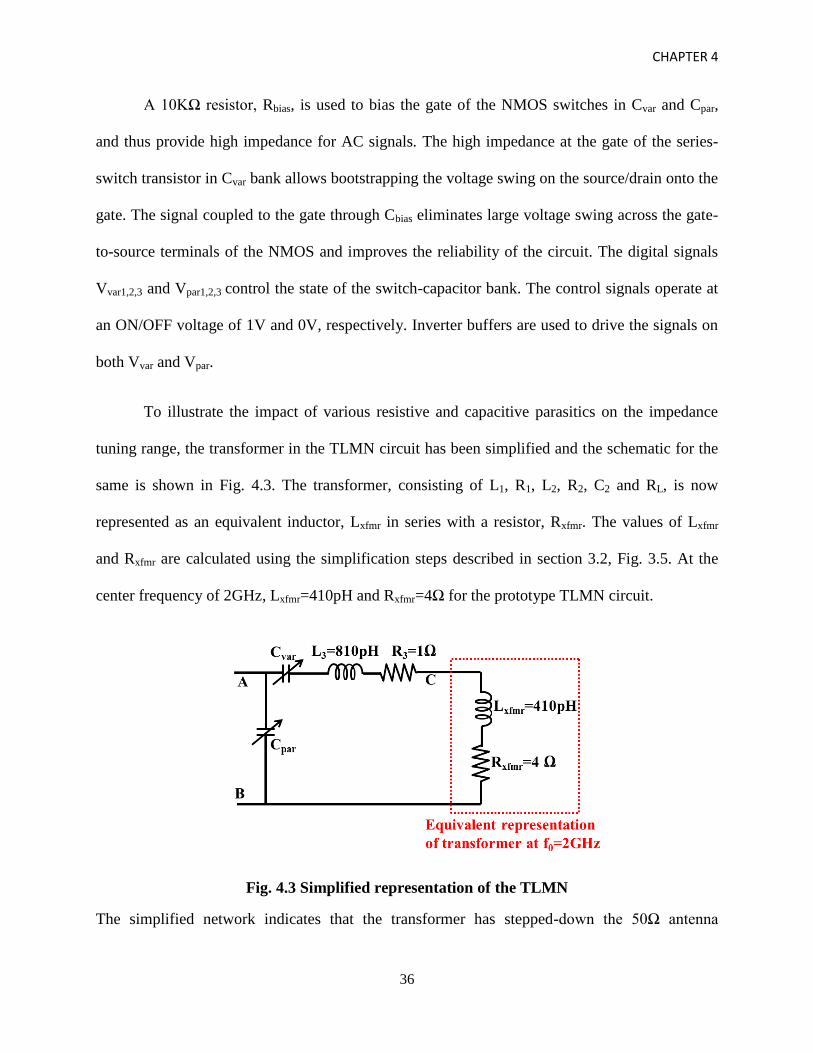
To illustrate the impact of various resistive and capacitive parasitics on the impedance
tuning range, the transformer in the TLMN circuit has been simplified and the schematic for the
same is shown in Fig. 4.3. The transformer, consisting of L1, R1, L2, R2, C2 and RL, is now
represented as an equivalent inductor, Lxfmr in series with a resistor, Rxfmr. The values of Lxfmr
and Rxfmr are calculated using the simplification steps described in section 3.2, Fig. 3.5. At the
center frequency of 2GHz, Lxfmr=410pH and Rxfmr=4Ω for the prototype TLMN circuit.
Fig. 4.3 Simplified representation of the TLMN
The simplified network indicates that the transformer has stepped-down the 50Ω antenna

CHAPTER 4
37
impedance to Rxfmr of 4Ω. The goal is to study the range of input impedance (Zin) that can be
obtained with a variable L-match, which is discussed in the next section.
4.1.2 Tuning Range Limitations using an L-match
From a circuit-theory perspective, there is no upper-bound on the impedance that can be
obtained from a tunable L-match made of ideal L and C components. However, for a practical
physical implementation of the TLMN in integrated-circuit form, it is important to analyze the
impact of three non-idealities. First, inductors have a finite quality factor of less than 10 or 12 at
radio frequencies. Second, the parallel-plate capacitors have parasitic bottom-plate capacitance
which can be 5-10% of the desired capacitance. Finally, any switch implementation using MOS
transistors must account for the fundamental trade-off between channel resistance in the ON state
and parasitic capacitance in the OFF state.
Upper Bound on Zin:
In Fig. 4.3, L3, Lxfmr, R3 and Rxfmr form a series R-L circuit with the quality factor of the
branch given as -
( )
( )
The purpose of Cvar in the L-match network is to modify the effective value of inductance L3.
Hence, if we consider the inductance L3 to be variable (achieved by varying Cvar), the resultant
impedance Zin, between nodes A and B, will be
Real ( ) ( ) ( )
where, Qser is variable and is determined by the variable inductance L3. From the expression for
Zin, it is obvious that higher values of input impedance Zin can be obtained by increasing the
inductance L3. However, assuming a constant quality factor, it is straight-forward to prove that
CHAPTER 4
38
an increase in L3 is also accompanied by a corresponding increase in the ESR, R3. From Fig. 4.3,
R3 appears in series with Rxfmr. An increase in R3 results in an increased insertion loss in the
TLMN. Thus, an upper bound on L3 is determined based on the maximum insertion loss
tolerable. And this maximum value of L3 places an upper bound on input impedance Zin.
The next component to consider is the series capacitance Cvar. Cvar is employed in the L-
match network to provide variable inductance L3 (by tuning the values of Cvar).Thus, the value of
Cvar will determine the effective value of L3 in the network indicated in Fig. 4.3. As explained in
the above paragraph, higher the value of effective L3, higher will be the input impedance Zin.
Therefore, a large capacitance value for Cvar will result in an increase in the effective inductance
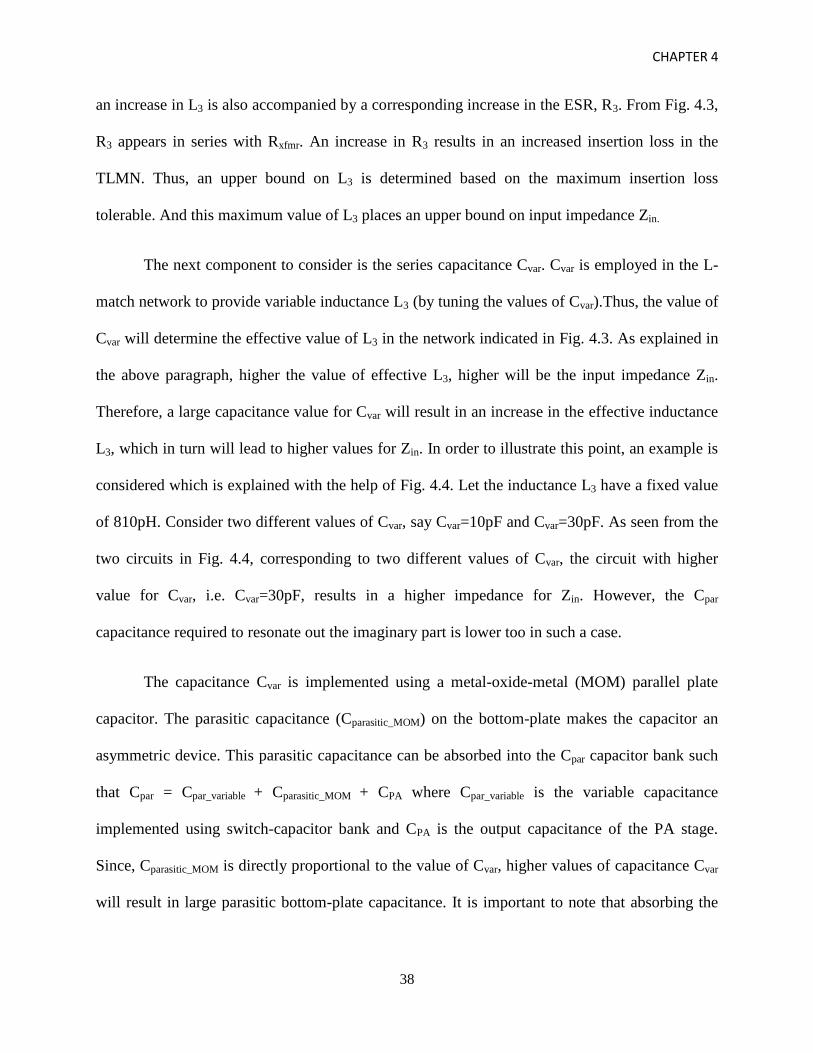
L3, which in turn will lead to higher values for Zin. In order to illustrate this point, an example is
considered which is explained with the help of Fig. 4.4. Let the inductance L3 have a fixed value
of 810pH. Consider two different values of Cvar, say Cvar=10pF and Cvar=30pF. As seen from the
two circuits in Fig. 4.4, corresponding to two different values of Cvar, the circuit with higher
value for Cvar, i.e. Cvar=30pF, results in a higher impedance for Zin. However, the Cpar
capacitance required to resonate out the imaginary part is lower too in such a case.
The capacitance Cvar is implemented using a metal-oxide-metal (MOM) parallel plate
capacitor. The parasitic capacitance (Cparasitic_MOM) on the bottom-plate makes the capacitor an
asymmetric device. This parasitic capacitance can be absorbed into the Cpar capacitor bank such
that Cpar = Cpar_variable + Cparasitic_MOM + CPA where Cpar_variable is the variable capacitance
implemented using switch-capacitor bank and CPA is the output capacitance of the PA stage.
Since, Cparasitic_MOM is directly proportional to the value of Cvar, higher values of capacitance Cvar
will result in large parasitic bottom-plate capacitance. It is important to note that absorbing the
CHAPTER 4
39
fixed capacitance Cparasitic_MOM into Cpar reduces the variable component of Cpar_variable. Therefore,
there exists an upper bound on the value of Cvar than can be realized in the TLMN.
Fig. 4.4 Illustration of tuning range limitation due to Cvar and Cpar values
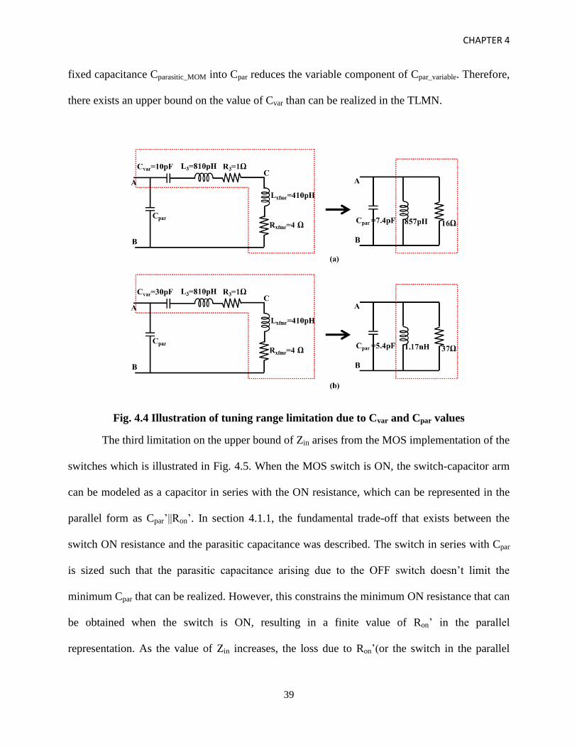
The third limitation on the upper bound of Zin arises from the MOS implementation of the
switches which is illustrated in Fig. 4.5. When the MOS switch is ON, the switch-capacitor arm
can be modeled as a capacitor in series with the ON resistance, which can be represented in the
parallel form as Cpar’||Ron’. In section 4.1.1, the fundamental trade-off that exists between the
switch ON resistance and the parasitic capacitance was described. The switch in series with Cpar
is sized such that the parasitic capacitance arising due to the OFF switch doesn’t limit the
minimum Cpar that can be realized. However, this constrains the minimum ON resistance that can
be obtained when the switch is ON, resulting in a finite value of Ron’ in the parallel
representation. As the value of Zin increases, the loss due to Ron’(or the switch in the parallel
CHAPTER 4
40
capacitor bank Cpar) increases, resulting in an increased insertion loss in the network. Thus, there
is a trade-off between the insertion loss and upper bound on Zin that can be obtained.
Fig. 4.5 (a) Switch-capacitor branch (b) Equivalent circuit when the switch is in ‘ON’ state
Lower Bound on Zin:
The lower range of impedance obtainable is limited by two factors- transformer turns
ratio and the parasitic capacitance in Cvar bank. The L-match networks can only step-up the
impedance that results from the fixed impedance translation from the transformer. The lower
bound on Zin is thus equal to Rxfmr (refer to Fig. 4.3). In the previous section, it was shown that
higher values of Cvar will result in higher values of Zin. Therefore, to obtain lower values of Zin,
the value of Cvar should be smaller. The dependence of the lower bound on Cvar’s parasitic
capacitance can be better illustrated with the help of Fig. 4.6. Assume C1, C2 and the series
switches constitute a switch-capacitor bank. The OFF NMOS transistor is modeled as a
capacitance, Cdrain, as shown in Fig. 4.6(b). When a switch is OFF, ideally it should provide an
open-circuit, or infinite impedance condition. However, due to parasitic capacitance Cdrain, the
OFF switch provides an input capacitance of (C1 series Cdrain) || (C2 series Cdrain). Thus, in the
Cvar and Cpar capacitor banks, the OFF transistor’s parasitic capacitor limits the minimum
CHAPTER 4
41
achievable capacitance value.
Fig. 4.6 (a) Switch-Capacitor Bank (b) Equivalent circuit when the switches are ‘OFF’
Considering the above mentioned trade-off, values of Cvar, Cpar and L3 have been chosen
to optimize both the tuning range and insertion loss. A tuning range of 1:4.8 has been obtained
using the TLMN. The loss in the transformer is 1.9dB. The switches and the ESR of L3 introduce
an additional loss of 1.5dB, resulting in a total loss of 3.4dB in the TLMN. In the next section,
design of the second tunable matching network namely, Transformer-plus-Pi-match-based
tunable matching network (TPMN) is discussed.
4.2 Transformer-plus-Pi-match-based tunable Matching
Network (TPMN)
In TPMN described in Fig. 4.7, the Pi-matching network provides impedance tunability.
Similar to the TLMN, the transformer steps-down the 50Ω antenna impedance to lower valued
impedance. The pi-network converts the fixed impedance resulting from the transformer network
to variable impedance by tuning the capacitor values in Cpar and Cvar capacitor banks.
4.2.1 Design details
The transformer used in the TLMN, described in sub-section 4.1, is also used in the
CHAPTER 4
42
design of the TPMN. The fixed inductance L3 and the variable capacitors, Cvar and Cpar, together
form a Pi-network. The variable capacitors are realized using switch-capacitor banks where the
switches are turned ON or OFF using digital control signals Vpar,1,2,3 & Vvar,1,2,3. The NMOS
switch control voltages are 1V and 0V in both the capacitor banks. The switch-size W1/L1 in the
capacitor bank Cvar is 2.5mm/40n and the switch size W2/L2 in the capacitor bank Cpar is
2mm/40n. These switch sizes are chosen to minimize the losses without increasing the parasitic
capacitance (explained in detail in section 4.2.2). Similar to the TLMN, Rbias and Cbias are used to
setup DC bias voltages for the NMOS switches and couple AC signal swing onto their gates.
Inverter buffers are used to drive both sets of switches. A value of 444pH is selected for
inductance L3 considering the tuning range versus insertion loss trade-off, which will be
explained in the next section (4.2.2)
Fig. 4.7 Circuit implementation of Transformer-plus-Pi-match-based tunable network
(TPMN)
CHAPTER 4
43
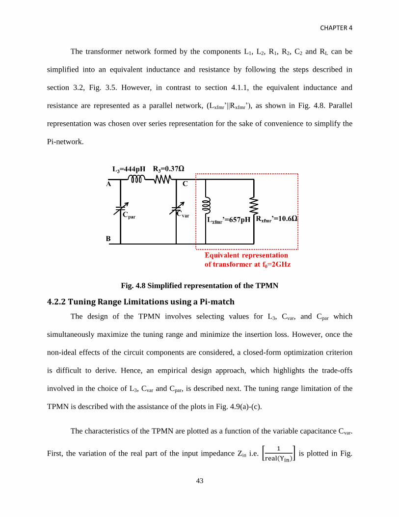
The transformer network formed by the components L1, L2, R1, R2, C2 and RL can be
simplified into an equivalent inductance and resistance by following the steps described in
section 3.2, Fig. 3.5. However, in contrast to section 4.1.1, the equivalent inductance and
resistance are represented as a parallel network, (Lxfmr’||Rxfmr’), as shown in Fig. 4.8. Parallel
representation was chosen over series representation for the sake of convenience to simplify the
Pi-network.
Fig. 4.8 Simplified representation of the TPMN
4.2.2 Tuning Range Limitations using a Pi-match
The design of the TPMN involves selecting values for L3, Cvar, and Cpar which
simultaneously maximize the tuning range and minimize the insertion loss. However, once the
non-ideal effects of the circuit components are considered, a closed-form optimization criterion
is difficult to derive. Hence, an empirical design approach, which highlights the trade-offs
involved in the choice of L3, Cvar and Cpar, is described next. The tuning range limitation of the
TPMN is described with the assistance of the plots in Fig. 4.9(a)-(c).
The characteristics of the TPMN are plotted as a function of the variable capacitance Cvar.
First, the variation of the real part of the input impedance Zin i.e. [
( )] is plotted in Fig.
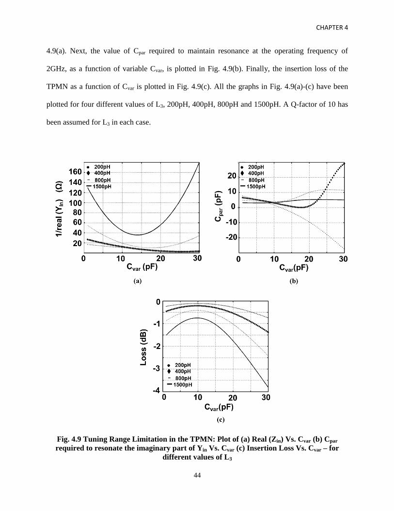
CHAPTER 4
44
4.9(a). Next, the value of Cpar required to maintain resonance at the operating frequency of
2GHz, as a function of variable Cvar, is plotted in Fig. 4.9(b). Finally, the insertion loss of the
TPMN as a function of Cvar is plotted in Fig. 4.9(c). All the graphs in Fig. 4.9(a)-(c) have been
plotted for four different values of L3, 200pH, 400pH, 800pH and 1500pH. A Q-factor of 10 has
been assumed for L3 in each case.
Fig. 4.9 Tuning Range Limitation in the TPMN: Plot of (a) Real (Zin) Vs. Cvar (b) Cpar
required to resonate the imaginary part of Yin Vs. Cvar (c) Insertion Loss Vs. Cvar – for
different values of L3
CHAPTER 4
45
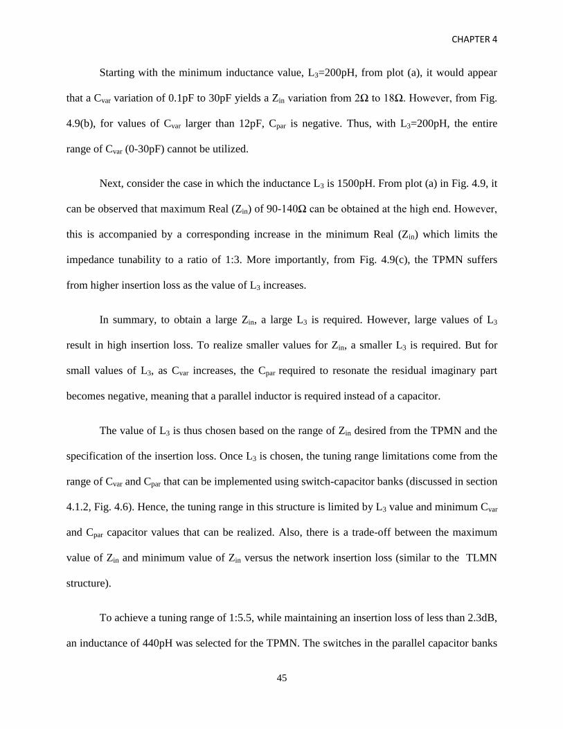
Starting with the minimum inductance value, L3=200pH, from plot (a), it would appear
that a Cvar variation of 0.1pF to 30pF yields a Zin variation from 2Ω to 18Ω. However, from Fig.
4.9(b), for values of Cvar larger than 12pF, Cpar is negative. Thus, with L3=200pH, the entire
range of Cvar (0-30pF) cannot be utilized.
Next, consider the case in which the inductance L3 is 1500pH. From plot (a) in Fig. 4.9, it
can be observed that maximum Real (Zin) of 90-140Ω can be obtained at the high end. However,
this is accompanied by a corresponding increase in the minimum Real (Zin) which limits the
impedance tunability to a ratio of 1:3. More importantly, from Fig. 4.9(c), the TPMN suffers
from higher insertion loss as the value of L3 increases.
In summary, to obtain a large Zin, a large L3 is required. However, large values of L3
result in high insertion loss. To realize smaller values for Zin, a smaller L3 is required. But for
small values of L3, as Cvar increases, the Cpar required to resonate the residual imaginary part
becomes negative, meaning that a parallel inductor is required instead of a capacitor.
The value of L3 is thus chosen based on the range of Zin desired from the TPMN and the
specification of the insertion loss. Once L3 is chosen, the tuning range limitations come from the
range of Cvar and Cpar that can be implemented using switch-capacitor banks (discussed in section
4.1.2, Fig. 4.6). Hence, the tuning range in this structure is limited by L3 value and minimum Cvar
and Cpar capacitor values that can be realized. Also, there is a trade-off between the maximum
value of Zin and minimum value of Zin versus the network insertion loss (similar to the TLMN
structure).
To achieve a tuning range of 1:5.5, while maintaining an insertion loss of less than 2.3dB,
an inductance of 440pH was selected for the TPMN. The switches in the parallel capacitor banks
CHAPTER 4
46
and ESR of L3 introduce 0.5dB loss while the transformer introduces 1.9dB loss.
4.3 Comparison between TLMN and TPMN
Transformer-plus-Pi-matched structure (TPMN) has several advantages when compared
to Transformer-plus-L-matched structure (TLMN).
a. DC-Bias functionality: The TLMN contains a series capacitor in the signal path. As a
result, in a fully-integrated differential PA system, the center-tap of the transformer in
the TLMN cannot be used to provide the supply bias. A separate DC choke
inductance has to be included in the PA for providing supply voltage. On the
contrary, the TPMN does not contain any series capacitance and does not need any
additional bias inductance.
b. ON-resistance of the switch: In the TPMN, the switches in both the Cvar and Cpar
capacitor banks are shunt switches with one terminal connected to the ground. With a
grounded source, the NMOS transistors are fully turned on independent of the input
signal level. In addition, there is no signal swing at the drain of the NMOS switch
when it is ON. This leads to constant switch resistance ensuring better linearity [15].
In contrast, the switches for Cvar bank in the TLMN are in the signal path and have
large voltage swings at both the drain and source nodes of the NMOS. Though a
coupling capacitor is added between the source and gate nodes of the NMOS switch,
to keep the switch ON at all signal levels, the value of the ON resistance varies
depending on the input signal strength. The ON resistance is also sensitive to the
parasitics occurring at the switch’s source/drain and gate nodes. Thus, the linearity of
the TLMN is not as good as the TPMN.
CHAPTER 4
47
c. Robustness of the network: The series switches in the TLMN pose another serious
problem. In the series switches in Cvar block, the bulk of the NMOS switch is locally
connected to its source. This is done with the intention of eliminating threshold
voltage increase due to different potentials at source and bulk terminals. Due to the
locally shorted bulk, the deep-nwell associated with the NMOS switch necessitates a
layout as shown in Fig. 4.11. There are two p-n junctions between the source/bulk
and p-substrate (ground) terminals which results in two diodes, a pwell-to-deep nwell
diode and a deep nwell-to-psub diode, in anti-series configuration as shown in Fig.
4.11. These diodes create depletion capacitance between the source and ground
nodes. This capacitance is modeled as the unwanted capacitance Cunwanted, indicated
between nodes C and B in Fig. 4.10 (highlighted in red). The unwanted capacitance
between nodes C and B alters the value of the input impedance Zin. Therefore, it is
necessary to account for this capacitance while designing the TLMN (Even if the bulk
is not shorted to ground, the source-to-bulk capacitance has the same undesired effect
as described above). The TPMN, on the other hand, is transparent to this Cunwanted
capacitance (occurring between the drain/source of the switch and substrate), as the
capacitance gets shorted out by the ON resistance of the switch. Hence, the TPMN is
more robust to parasitics arising due to the internal diodes in NMOS switches.
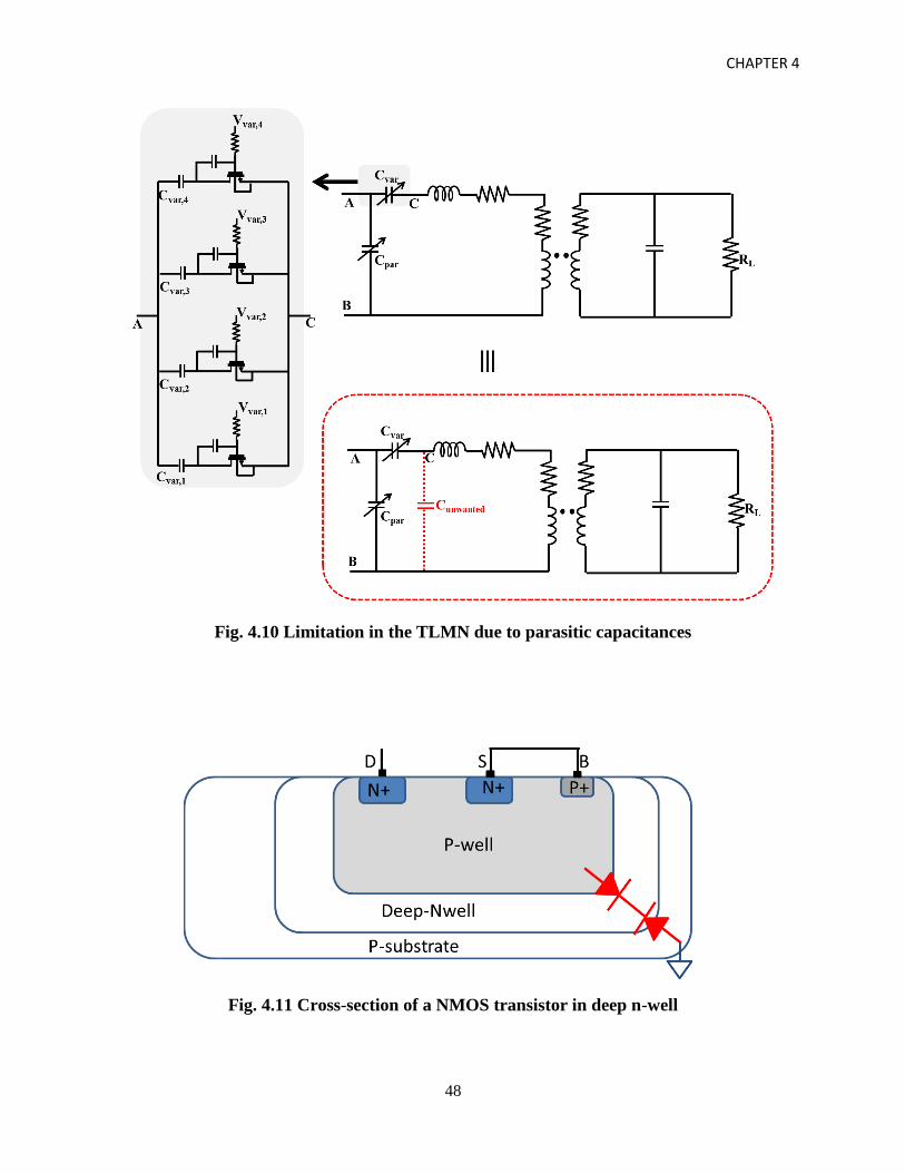
CHAPTER 4
48
Fig. 4.10 Limitation in the TLMN due to parasitic capacitances
Fig. 4.11 Cross-section of a NMOS transistor in deep n-well
CHAPTER 4
49
In summary, by using a set of switch-capacitor banks to realize a variable capacitance,
two tunable matching networks have been implemented in bulk-CMOS process. The two
networks have a 100MHz bandwidth of operation, with a center frequency around 2GHz. Since
the control voltages for all the switches are 1V, the tuning networks are ideal for integration with
lower sub-nanometer CMOS process nodes where the supply voltages are limited to 1V or 1.2V.
The transformer in the tunable matching network has been designed for minimum insertion loss
while the L/Pi-networks have been optimized for both tuning range as well as insertion loss. The
variable capacitors in this work are selected to obtain real impedance Zin for all switch settings
while maintaining the imaginary part of the impedance at 0Ω. However, a variable imaginary
part can be obtained as well, by aptly varying the capacitors in the switch-capacitor banks. The
two matching networks are ideal for use as PA output matching network where a variable Rout
needs to be presented to the PA. The concepts described in this chapter and the tunable networks
developed can be used for other applications as well by tailoring the networks to meet the
specific demands of the application.
In the next chapter, simulation results for the two tunable matching networks are
presented.
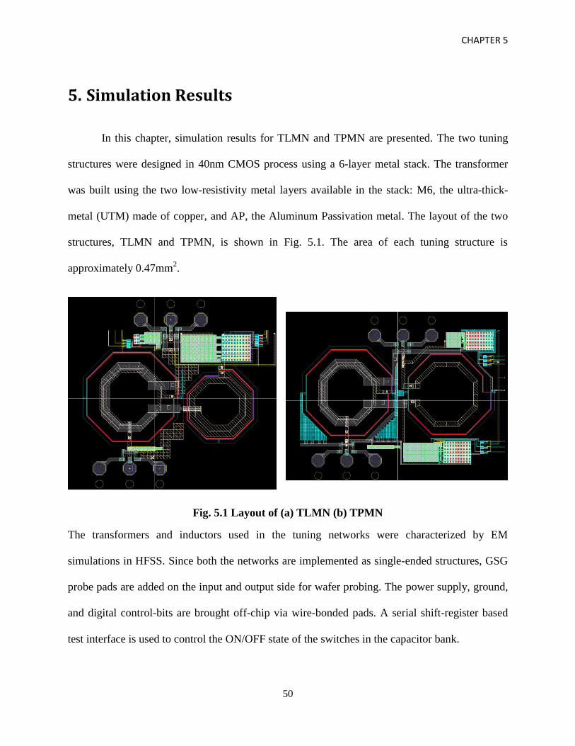
CHAPTER 5
50
5. Simulation Results
In this chapter, simulation results for TLMN and TPMN are presented. The two tuning
structures were designed in 40nm CMOS process using a 6-layer metal stack. The transformer
was built using the two low-resistivity metal layers available in the stack: M6, the ultra-thick-
metal (UTM) made of copper, and AP, the Aluminum Passivation metal. The layout of the two
structures, TLMN and TPMN, is shown in Fig. 5.1. The area of each tuning structure is
approximately 0.47mm2.
Fig. 5.1 Layout of (a) TLMN (b) TPMN
The transformers and inductors used in the tuning networks were characterized by EM
simulations in HFSS. Since both the networks are implemented as single-ended structures, GSG
probe pads are added on the input and output side for wafer probing. The power supply, ground,
and digital control-bits are brought off-chip via wire-bonded pads. A serial shift-register based
test interface is used to control the ON/OFF state of the switches in the capacitor bank.
CHAPTER 5
51
The tuning networks described in this section have application between the PA output
and the antenna. Therefore, the main parameter of interest is the range of real input impedance
that can be realized while maintaining a zero imaginary part. Another possible application of the
tunable matching network techniques proposed in this work would be for dynamic load
modulation for efficiency improvement. In such a system, the impedance presented to the PA is
modulated as a function of the input signal strength to maintain PA operation at peak efficiency.
Variation in the phase of S21, resulting due to impedance tuning, translates to a signal dependent
phase delay, resulting in inter-symbol interference (ISI) [14]. Hence, if dynamic load modulation
is desired, the variation in the phase of S21 should be as low as possible. For high power
application, it is important that the tuning network does not limit the compression point of the
PA. The next two sections provide the performance of the two networks in the areas discussed
above. Both these networks are characterized with a 50Ω load to mimic the effect of the antenna
impedance.
5.1 Simulation results of the TLMN
The TLMN impedance tuning network comprises of a 4-bit capacitor bank along the
series path, and 3-bit capacitor bank in the shunt path. Seven independent bit settings yield 27
unique input impedance (Zin) values. However, as described previously, at the output of the PA it
is important to modulate the real-part of the input impedance with minimal variation in the
imaginary part. The magnitude and phase of the input impedance for four states of the TLMN
which yields very small imag(Zin) are plotted in Fig. 5.2. The magnitude, and phase of Zin versus
frequency is shown in Fig. 5.2(a) and Fig. 5.2(b), respectively.
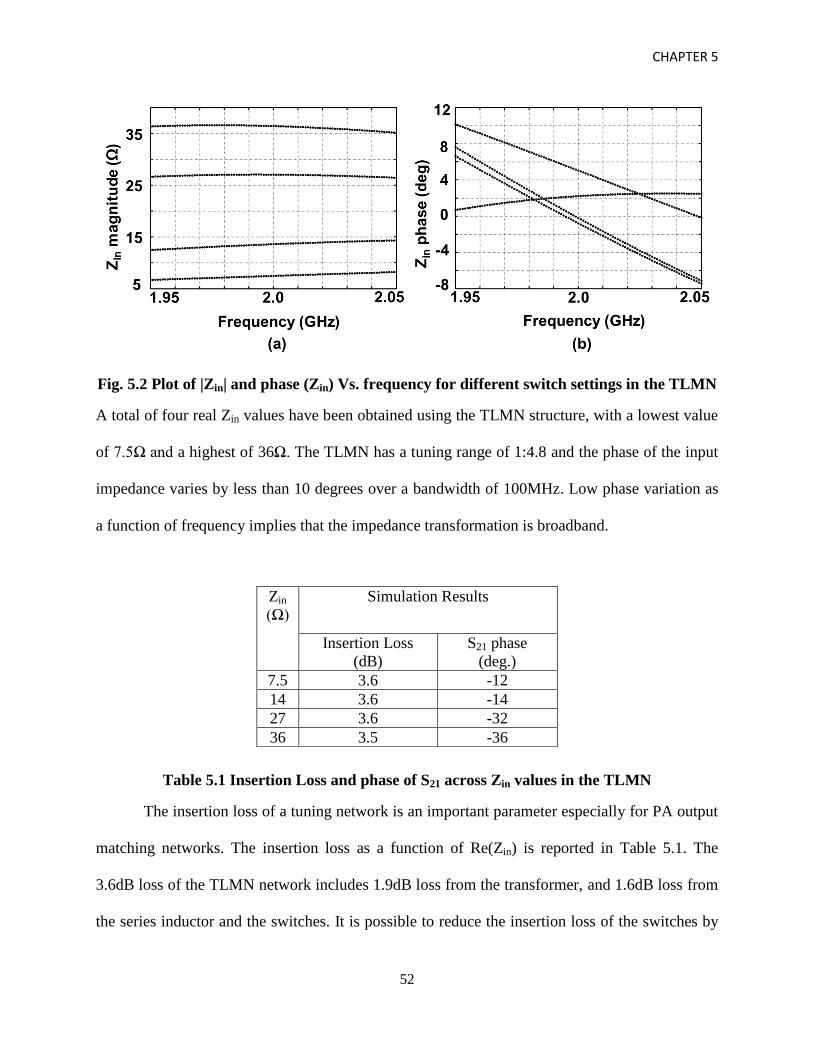
CHAPTER 5
52
Fig. 5.2 Plot of |Zin| and phase (Zin) Vs. frequency for different switch settings in the TLMN
A total of four real Zin values have been obtained using the TLMN structure, with a lowest value
of 7.5Ω and a highest of 36Ω. The TLMN has a tuning range of 1:4.8 and the phase of the input
impedance varies by less than 10 degrees over a bandwidth of 100MHz. Low phase variation as
a function of frequency implies that the impedance transformation is broadband.
Table 5.1 Insertion Loss and phase of S21 across Zin values in the TLMN
The insertion loss of a tuning network is an important parameter especially for PA output
matching networks. The insertion loss as a function of Re(Zin) is reported in Table 5.1. The
3.6dB loss of the TLMN network includes 1.9dB loss from the transformer, and 1.6dB loss from
the series inductor and the switches. It is possible to reduce the insertion loss of the switches by
Zin
(Ω)
Simulation Results
Insertion Loss
(dB)
S21 phase
(deg.)
7.5 3.6 -12
14 3.6 -14
27 3.6 -32
36 3.5 -36
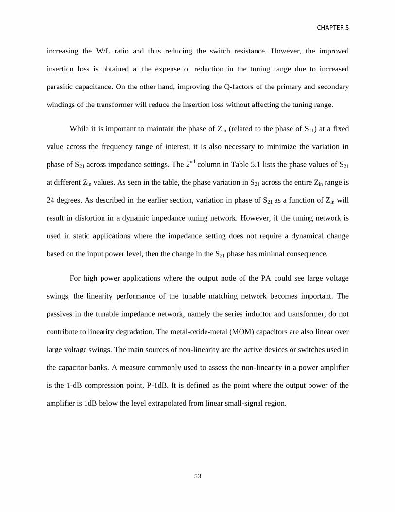
CHAPTER 5
53
increasing the W/L ratio and thus reducing the switch resistance. However, the improved
insertion loss is obtained at the expense of reduction in the tuning range due to increased
parasitic capacitance. On the other hand, improving the Q-factors of the primary and secondary
windings of the transformer will reduce the insertion loss without affecting the tuning range.
While it is important to maintain the phase of Zin (related to the phase of S11) at a fixed
value across the frequency range of interest, it is also necessary to minimize the variation in
phase of S21 across impedance settings. The 2nd
column in Table 5.1 lists the phase values of S21
at different Zin values. As seen in the table, the phase variation in S21 across the entire Zin range is
24 degrees. As described in the earlier section, variation in phase of S21 as a function of Zin will
result in distortion in a dynamic impedance tuning network. However, if the tuning network is
used in static applications where the impedance setting does not require a dynamical change
based on the input power level, then the change in the S21 phase has minimal consequence.
For high power applications where the output node of the PA could see large voltage
swings, the linearity performance of the tunable matching network becomes important. The
passives in the tunable impedance network, namely the series inductor and transformer, do not
contribute to linearity degradation. The metal-oxide-metal (MOM) capacitors are also linear over
large voltage swings. The main sources of non-linearity are the active devices or switches used in
the capacitor banks. A measure commonly used to assess the non-linearity in a power amplifier
is the 1-dB compression point, P-1dB. It is defined as the point where the output power of the
amplifier is 1dB below the level extrapolated from linear small-signal region.
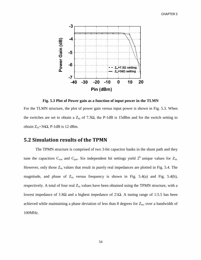
CHAPTER 5
54
Fig. 5.3 Plot of Power gain as a function of input power in the TLMN
For the TLMN structure, the plot of power gain versus input power is shown in Fig. 5.3. When
the switches are set to obtain a Zin of 7.5Ω, the P-1dB is 15dBm and for the switch setting to
obtain Zin=36Ω, P-1dB is 12 dBm.
5.2 Simulation results of the TPMN
The TPMN structure is comprised of two 3-bit capacitor banks in the shunt path and they
tune the capacitors Cvar and Cpar. Six independent bit settings yield 26
unique values for Zin.
However, only those Zin values that result in purely real impedances are plotted in Fig. 5.4. The
magnitude, and phase of Zin versus frequency is shown in Fig. 5.4(a) and Fig. 5.4(b),
respectively. A total of four real Zin values have been obtained using the TPMN structure, with a
lowest impedance of 3.8Ω and a highest impedance of 21Ω. A tuning range of 1:5.5 has been
achieved while maintaining a phase deviation of less than 8 degrees for Zin, over a bandwidth of
100MHz.
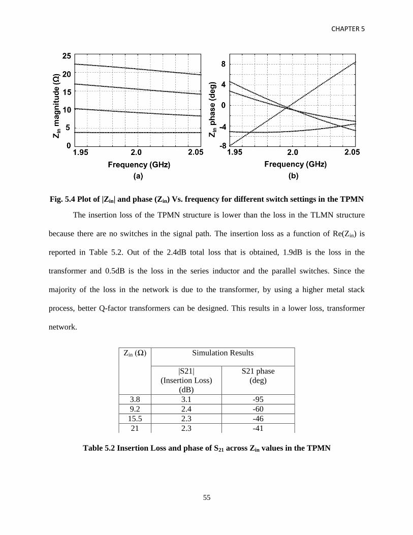
CHAPTER 5
55
Fig. 5.4 Plot of |Zin| and phase (Zin) Vs. frequency for different switch settings in the TPMN
The insertion loss of the TPMN structure is lower than the loss in the TLMN structure
because there are no switches in the signal path. The insertion loss as a function of Re(Zin) is
reported in Table 5.2. Out of the 2.4dB total loss that is obtained, 1.9dB is the loss in the
transformer and 0.5dB is the loss in the series inductor and the parallel switches. Since the
majority of the loss in the network is due to the transformer, by using a higher metal stack
process, better Q-factor transformers can be designed. This results in a lower loss, transformer
network.
Table 5.2 Insertion Loss and phase of S21 across Zin values in the TPMN
Zin (Ω) Simulation Results
|S21|
(Insertion Loss)
(dB)
S21 phase
(deg)
3.8 3.1 -95
9.2 2.4 -60
15.5 2.3 -46
21 2.3 -41
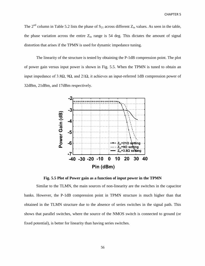
CHAPTER 5
56
The 2nd
column in Table 5.2 lists the phase of S21 across different Zin values. As seen in the table,
the phase variation across the entire Zin range is 54 deg. This dictates the amount of signal
distortion that arises if the TPMN is used for dynamic impedance tuning.
The linearity of the structure is tested by obtaining the P-1dB compression point. The plot
of power gain versus input power is shown in Fig. 5.5. When the TPMN is tuned to obtain an
input impedance of 3.8Ω, 9Ω, and 21Ω, it achieves an input-referred 1dB compression power of
32dBm, 21dBm, and 17dBm respectively.
Fig. 5.5 Plot of Power gain as a function of input power in the TPMN
Similar to the TLMN, the main sources of non-linearity are the switches in the capacitor
banks. However, the P-1dB compression point in TPMN structure is much higher than that
obtained in the TLMN structure due to the absence of series switches in the signal path. This
shows that parallel switches, where the source of the NMOS switch is connected to ground (or
fixed potential), is better for linearity than having series switches.
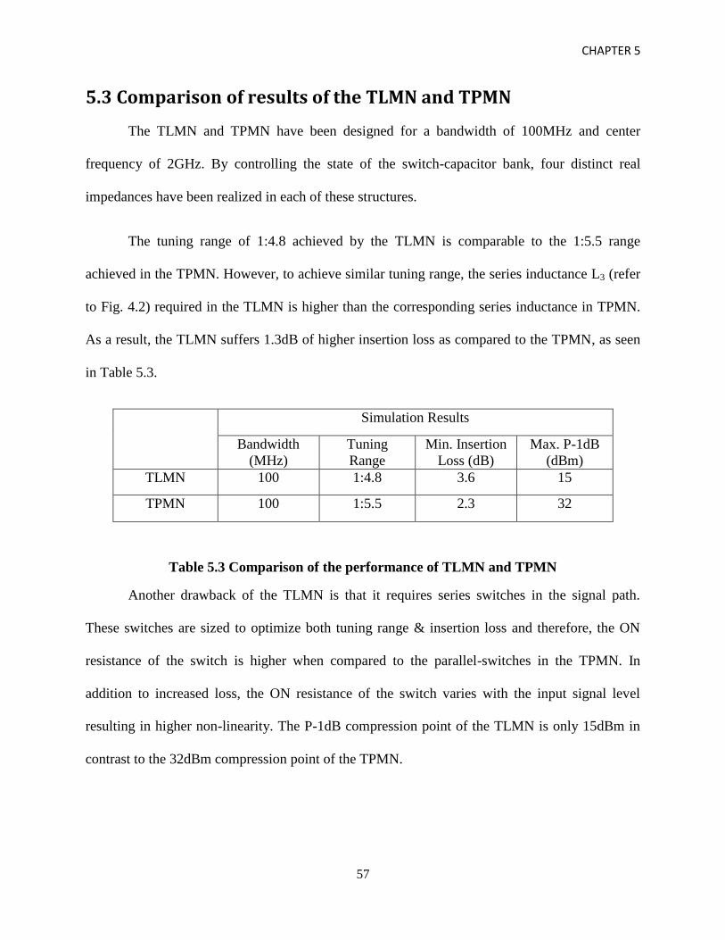
CHAPTER 5
57
5.3 Comparison of results of the TLMN and TPMN
The TLMN and TPMN have been designed for a bandwidth of 100MHz and center
frequency of 2GHz. By controlling the state of the switch-capacitor bank, four distinct real
impedances have been realized in each of these structures.
The tuning range of 1:4.8 achieved by the TLMN is comparable to the 1:5.5 range
achieved in the TPMN. However, to achieve similar tuning range, the series inductance L3 (refer
to Fig. 4.2) required in the TLMN is higher than the corresponding series inductance in TPMN.
As a result, the TLMN suffers 1.3dB of higher insertion loss as compared to the TPMN, as seen
in Table 5.3.
Simulation Results
Bandwidth
(MHz)
Tuning
Range
Min. Insertion
Loss (dB)
Max. P-1dB
(dBm)
TLMN 100 1:4.8 3.6 15
TPMN 100 1:5.5 2.3 32
Table 5.3 Comparison of the performance of TLMN and TPMN
Another drawback of the TLMN is that it requires series switches in the signal path.
These switches are sized to optimize both tuning range & insertion loss and therefore, the ON
resistance of the switch is higher when compared to the parallel-switches in the TPMN. In
addition to increased loss, the ON resistance of the switch varies with the input signal level
resulting in higher non-linearity. The P-1dB compression point of the TLMN is only 15dBm in
contrast to the 32dBm compression point of the TPMN.
CHAPTER 6
58
6. Conclusion
In this work, two tunable matching networks, designed with the explicit goal of providing
large impedance-tunability and low insertion loss, at a fixed resonant frequency have been
proposed. Both the matching networks, TLMN and TPMN, are fully-integrated and prototype
test-chips have been realized in a 40nm bulk CMOS process.
The TLMN comprises of a transformer followed by an L-match and the TPMN
comprises of a transformer followed by a Pi-match. In both the networks, the transformer
provides a fixed impedance transformation, and the switch-capacitance based L/Pi-network
provides a variable impedance transformation. A design methodology highlighting the loss
mechanism in transformer-based matching networks is presented. Based on this methodology,
circuit conditions to obtain minimum insertion loss are derived.
The TLMN and TPMN achieve an impedance transformation ratio greater than 12 and
tuning ranges of 1:4.8 and 1:5.5, respectively. The minimum insertion loss of the entire network
is 2.3dB with switches contributing to less than 25% of the loss. The P-1dB compression point
for the TLMN and TPMN is 15dBm and 32dBm, respectively. The switch-capacitor banks in
both the tuning networks have been designed to ensure all reliability constraints are satisfied,
with the control voltage for the switches being 1V.
A logical extension to the work presented in this thesis would be to build a complete
transmit system in which TLMN/TPMN are part of fully-integrated, closed-loop dynamic load
modulation system. Ideally, in a dynamic load modulation system, the transformation ratio of the
matching network will be a function of the input power to the power amplifier. Modulation
CHAPTER 6
59
techniques such as OFDM, with large peak-to-average ratio, can potentially exploit dynamic load
modulation to maximize the power efficiency of the PA in back-off.
A switch-based capacitor bank lies at the heart of the tunable matching network
technique described in this work. However, a switch-based capacitor can only be tuned over a
discrete set of values. In order to obtain dynamic load modulation, continuous tunability is
required. Though varactors are advantageous in this scenario, the non-linearity introduced by
them must be analyzed carefully. The capacitance realized by the varactor is dependent on the
voltage swing appearing across it. Since the matching network is employed at the PA output,
large voltage swings occur across the varactor. An interesting technique to solve this problem
would be to employ the varactor in conjunction with switch-capacitor banks. The switch-
capacitors can be used for selecting an appropriate range of capacitance while the varactor can be
used for fine tuning of the capacitance. Thus, by restricting the capacitance obtained from the
varactor to a small fraction of the total desired value, the non-linearity arising due to it can be
minimized.
60
References
[1] W. Wesson et al., “A long-range, fully-integrated, regulator-less CMOS Power Amplifier for
Wireless Sensor Communications”, IEEE Radio Frequency Integrated Circuits Symposium
Dig. of papers, pp. 145-148, Jun 2012
[2] K.R. Boyle et al., “Analysis of Mobile Phone Antenna Impedance Variations with User
Proximity” IEEE Transactions on Antennas and Propagation, Vol. 55, No. 2, pp. 364-372,
Feb 2007
[3] D. M. Pozar, “Microwave Engineering” 3rd
ed., Wiley, 2004
[4] A. Keerti et al., “RF Characterization of SiGe HBT Power Amplifiers Under Load
Mismatch” IEEE Transactions on Microwave Theory and Techniques, Vol. 55, No. 2, pp.
207-214, Feb 2007
[5] B. Jiang et al., “Energy Scavenging for Inductively Coupled Passive RFID Systems” IEEE
Transactions on Instrumentation and Measurement, Vol. 56, No. 1, pp. 118-125, Feb 2007
[6] S. Cripps, “RF Power Amplifiers for Wireless Communications”, 2nd
ed. Norwood, MA:
Artech House, 2002
[7] A.M. Niknejad, “Electromagnetics for High-Speed Analog and Digital Communication
Circuits”, Cambridge University Press, 2007
[8] G. Hanington et al., “High-Efficiency Power Amplifier Using Dynamic Power-Supply
Voltage for CDMA Applications” IEEE Transactions on Microwave Theory and Techniques,
Vol. 47, No. 8, pp. 1471-1476, Aug 1999
[9] H. Wang et al., “A CMOS Broadband Power Amplifier With a Transformer-Based High-
Order Output Matching Network” IEEE Journal of Solid-State Circuits, Vol. 45, No. 12, pp.
2709-2722, Dec 2010
[10] H. M. Nemati et al., “Design of Varactor-Based Tunable Matching Networks for Dynamic
Load Modulation of High Power Amplifiers” IEEE Transactions on Microwave Theory and
Techniques, Vol. 57, No. 5, pp. 1110-1118, May 2009
[11] F. H. Raab “High-Efficiency Linear Amplification by Dynamic Load Modulation” IEEE
MTT-S International Microwave Symposium Digest, pp. 1717-1720, Jun 2003
[12] Bluetooth SIG, “Bluetooth Core Specification Addendum 3 rev. 2”, Jul 2012
https://www.bluetooth.org/en-us/specification/adopted-specifications
61
[13] Std. IEEE 802.11-2009, IEEE Standard for Information Technology-Telecommunications
and information exchange between systems Local and metropolitan area networks—Specific
Requirements Part 11: Wireless LAN Medium Access Control (MAC) and Physical Layer
(PHY) Specifications
[14] W.C. Edmund Neo et al., “Adaptive Multi-Band Multi-mode Power Amplifier using
Integrated Varactor-based Tunable Matching Networks” IEEE Journal of Solid-State
Circuits, Vol. 41, No. 9, pp. 2166-2176, Sep 2006
[15] P. Sjoblom et al., “An Adaptive Impedance Tuning CMOS circuit for ISM 2.4-GHz Band”
IEEE Transactions on Circuits and Systems-I: Regular papers, Vol. 52, No. 6, pp. 1115-
1124, Jun 2005
[16] J. Fu et al., “Improving Power Amplifier Efficiency and Linearity using a Dynamically
Controlled Tunable Matching Network” IEEE Transactions on Microwave Theory and
Techniques, Vol. 56, No. 12, pp. 3239-3244, Dec 2008
[17] X. Yu et al., “A 2-11 GHz Reconfigurable Multi-Mode LNA in 0.13µm CMOS” IEEE
Radio Frequency Integrated Circuits Symposium Dig. of papers, pp. 475-478, Jun 2012
[18] W. Li et al., “A 2.4-GHz/3.5-GHz/5-GHz Multi-Band LNA with Complementary Switched
Capacitor Multi-Tap Inductor in 0.18um CMOS” International Symposium on VLSI Design,
Automation and Test, pp. 1-4, Apr 2006
[19] X. Yu et al., “Integrated Multi-Tap Transformer for Reconfigurable Multimode Matching
Networks” International Symposium on Circuits and Systems, pp. 1395-1398, May 2011
[20] G. Cusmai et al., “A Magnetically Tuned Quadrature Oscillator” IEEE Journal of Solid-
State Circuits, Vol. 42, No. 12, pp. 2870-2877, Dec 2007
[21] R.G. Meyer et al., “Distortion in Variable-Capacitance Diodes” IEEE Journal of Solid-State
Circuits, Vol. 10, No. 1, pp. 47-54, Feb 1975
[22] K. Buisman et al., “Distortion Free Varactor Diode Topologies for RF Adaptivity” IEEE
MTT-S International Microwave Symposium Digest, pp. 157-160, Jun 2005
[23] Y. Han et al., “Analysis and Design of High Efficiency Matching Networks” IEEE
Transactions on Power Electronics, Vol. 21, No. 5, pp. 1484-1491, Sep 2006
[24] I. Aoki et al., “Distributed Active Transformer—A New Power-Combining and Impedance-
Transformation Technique” IEEE Transactions on Microwave Theory and Techniques, Vol.
50, No. 1, pp. 316-331, Jan 2002
62
[25] H. Gan “On-Chip Transformer Modeling, Characterization, and Applications in Power and
Low Noise Amplifiers”, Ph.D. Dissertation, Stanford University, 2006
[26] A.M. Niknejad et al., “Analysis, Design and Optimization of Spiral Inductors and
Transformers for Si RF IC’s” IEEE Journal of Solid-State Circuits, Vol. 33, No. 10, pp.
1470-1481, Oct 1998
[27] K.T. Ng et al., “Substrate Effects in Monolithic RF Transformers on Silicon” IEEE
Transactions on Microwave Theory and Techniques, Vol. 50, No. 1, pp. 377-383, Jan 2002
[28] J.R. Long “Monolithic Transformers for Silicon RF IC Design” IEEE Journal of Solid-State
Circuits, Vol. 35, No. 9, pp. 1368-1382, Sep 2000
[29] H. Cao et al., “Linearization of Efficiency-Optimized Dynamic Load Modulation
Transmitter Architectures” IEEE Transactions on Microwave Theory and Techniques, Vol.
58, No. 4, pp. 873-881, Apr 2010
[30] Y. Palaskas et al., “A 5-GHz 20-dBm Power Amplifier With Digitally Assisted AM-PM
Correction in a 90-nm CMOS Process” IEEE Journal of Solid-State Circuits, Vol. 41, No. 8,
pp. 1757-1763, Aug 2006
[31] H. Samavati et al., “Fractal Capacitors” IEEE Journal of Solid-State Circuits, Vol. 33, No.
12, pp. 2035-2041, Dec 1998