Embed Size (px)
Citation preview

©Copyright 2012
Irene Cheryl Wang

Material Characterization of Electrodeposited Copper-Nickel
Nanolaminated Alloy by SEM, EDS, and XRD
Irene Cheryl Wang
A thesis
submitted in partial fulfillment of the
requirements for the degree of
Master of Science in Materials Science and Engineering
University of Washington
2012
Committee:
Brian Flinn
Lucien Brush
Jihui Yang
Program Authorized to Offer Degree:
Materials Science & Engineering

University of Washington
Abstract
Material Characterization of Electrodeposited Copper-Nickel
Nanolaminated Alloy by SEM, EDS, and XRD
Irene Cheryl Wang
Chair of the Supervisory Committee:
Associate Professor Brian Flinn
Materials Science & Engineering
Electrodeposited nanolaminated copper-nickel alloys (Cu-Ni) exhibit excellent mechanical
properties due to their modulated structure and nanocrystalline microstructure. X-ray
diffraction, scanning electron microscopy, and energy dispersive X-ray spectroscopy were used
to characterize the composition, grain size, phases, and laminate structure of a nanolaminated
deposit to explore structure-process-property relationships. The processing method of interest
was pulse current electrodeposition of Cu-Ni a rotating disk electrode (RDE) with increased
rotation speed during deposition of Cu-rich layers. Although copper content was enhanced in
this way, it also caused macroscopic swirls in the deposit’s surface, which were reflected
microstructurally as Cu-rich streaks, non-planar layers, and other inhomogeneous morphology
in the nanolaminate coating. Bulk composition of the nanolaminate was calculated from XRD
spectra as being over 67wt%Ni overall, with over 91wt% Ni in Ni-rich layers and over 43wt% Ni
in Cu-rich layers. EDS data of the same deposit differed significantly from these values,
suggesting an overall composition closer to 55 wt% Ni, with a Ni-rich layer composition of 81
wt% Ni and 8.4 wt% Ni in the Cu-rich layers. Grain sizes of 15.8-22.3 nm were calculated for the
nanolaminated deposit compared to 13-19 nm grains in a monolithic Ni-rich deposit of Cu-Ni.

i
Table of Contents
List of Figures ...................................................................................................................................ii
List of Tables ................................................................................................................................... iv
Glossary ............................................................................................................................................ v
1. Introduction ............................................................................................................................. 1
1.1. Background Information .................................................................................................. 1
1.2. Basics of Electrodeposition .............................................................................................. 3
1.3. Motivation and Objectives ............................................................................................... 4
1.3.1. Composition .............................................................................................................. 6
1.3.2. Grain Size .................................................................................................................. 9
1.3.3. Phase Identification .................................................................................................. 9
1.3.4. Laminate Structure ................................................................................................. 15
2. Materials ................................................................................................................................ 17
3. Experimental Procedures ...................................................................................................... 19
3.1. X-ray Diffraction ............................................................................................................. 19
3.2. Sample Preparation ........................................................................................................ 20
3.3. Scanning Electron Microscopy and Energy Dispersive X-ray Spectroscopy................... 23
4. Results and Discussion ........................................................................................................... 24
4.1. Laminate Structures from SEM ...................................................................................... 24
4.2. Phase Identification from XRD ....................................................................................... 33
4.3. Composition from XRD and EDS ..................................................................................... 36
4.4. Grain Sizes from XRD and SEM ....................................................................................... 38
5. Conclusions ............................................................................................................................ 42
6. Future Work ........................................................................................................................... 43
References .................................................................................................................................... 44

ii
List of Figures
Figure 1. Crack redirection in a nanolaminated metallic system ................................................... 1
Figure 2. Comparison of pitting propagation in nanolaminate (left) vs. monolithic alloys (right) in
a corrosive environment ................................................................................................................. 2
Figure 3. Nanolamination created in Cu-Ni alloys by current density modulation during
electrodeposition ............................................................................................................................ 3
Figure 4. Electrodeposition set-up for plating a cathodic substrate with metallic deposit "M" .... 4
Figure 5. Motivation: characterization of the Cu-Ni nanolaminate system relating processing to
structure .......................................................................................................................................... 5
Figure 6. Characterization methods used to examine structural properties in the Cu-Ni
nanolaminate system ...................................................................................................................... 6
Figure 7. Lattice constants of some metallic solid solutions based on Vegard's law (dot-dash line)
......................................................................................................................................................... 8
Figure 8. XRD spectra for nanolaminated Cu-Ni films deposited with varying current density
[Baskaran 2006] ............................................................................................................................ 10
Figure 9. XRD spectrum for monolithic Cu-Ni showing locations of pure constituent peaks in
relation to those of the alloy [Bonou 1994] ................................................................................. 11
Figure 10. XRD spectrum of monolithic Ni-rich deposits made with pulsed current ................... 12
Figure 11. XRD spectrum for nanolaminated Cu-Ni films [Rajasekaran 2009] ............................. 13
Figure 12. XRD spectrum for nanolaminated Cu-Ni from [Ebrahimi 2001] .................................. 14
Figure 13. SEM images of layers in a nanolaminated Cu-Ni coating [Kaneko 2005] .................... 15
Figure 14. Microscopy resolution ranges ..................................................................................... 16
Figure 15. SEM images of as-deposited monolithic nanocrystalline Cu-Ni alloys from (left) a
saccharin-free plating bath and (right) saccharin-containing bath [Pellicer 2001] ...................... 16
Figure 16. As-deposited coating surfaces from rotating disk electrode samples ........................ 17
Figure 17. Orientation of XRD samples during testing ................................................................. 19
Figure 18. Nanolaminated and monolithic X-ray diffraction samples .......................................... 20
Figure 19. Diagram showing layer elongation created by angling the surface of the
nanolaminated sample "OBL LAM A" ........................................................................................... 21
Figure 20. Orientations of the electrodeposited sample beams mounted in bakelite pucks ...... 22
Figure 21. SEM image of etched polycrystalline copper substrate grains and contrast between
coating and substrate ................................................................................................................... 24
Figure 22. Measured and actual layer thicknesses on OBL LAM A under SEM at 20,000X
magnification ................................................................................................................................ 25
Figure 23. SEM images of measured layer thicknesses in LAM C at 30,000X magnification ....... 25
Figure 24. Macroscopic swirls in coating of nanolaminate deposit ............................................. 26

iii
Figure 25. Streaks in nanolaminate coating (LAM A sample) at 50X magnification ..................... 27
Figure 26. Optical micrograph of Cu-rich streaks seen across LAM A deposit at 5X magnification
....................................................................................................................................................... 27
Figure 27. SEM image of OBL LAM A showing streaks in the coating and contrast ..................... 28
Figure 28. SEM image of OBL LAM A showing detailed view of streaks in the coating at 1000X
magnification ................................................................................................................................ 29
Figure 29. Non-planar layers in SEM image of OBL LAM A at 2,000X magnification near the
substrate ....................................................................................................................................... 30
Figure 30. Layer inhomogeneity seen in LAM A under SEM at 1,300X magnification ................. 31
Figure 31. SEM image of LAM A coating showing delamination and regions of pitting at the .... 32
Figure 32. XRD spectrum for monolithic Ni-rich sample .............................................................. 33
Figure 33. XRD diffraction profile overlay of (Cu2Ni23)0.16 on the monolithic Ni-rich sample
spectrum ....................................................................................................................................... 34
Figure 34. XRD spectrum for nanolaminated sample ................................................................... 35
Figure 35. Phases identified from XRD spectrum for elemental composition of the
nanolaminated sample ................................................................................................................. 35
Figure 36. SEM image of monolithic Ni-rich coating showing spongy-like texture of round
protrusions and pits at 60,000x magnification ............................................................................. 39
Figure 37. Spherical pits and uniform texture observed in Ni-rich top coat of OBL LAM A under
SEM at 10,000X magnification ...................................................................................................... 40
Figure 38. SEM image of LAM A near substrate showing round pits at 50,000X magnification .. 40
Figure 39. SEM image of round pits between etched layers of OBL LAM A ................................. 41

iv
List of Tables
Table 1. Average layer thicknesses and calculated volume fractions of each phase ................... 26
Table 2. Phases identified from XRD spectrum for elemental composition of monolithic Ni-rich
sample ........................................................................................................................................... 34
Table 3. Quantitative XRD data for monolithic Ni-rich sample .................................................... 36
Table 4. Quantitative XRD data for nanolaminated sample ......................................................... 36
Table 5. Copper content of Cu-rich layers from EDS analysis and calculated from XRD data ..... 37

v
Glossary
nanolaminated alloy – an alloy which consists of alternating layers of metallic compositions
with nanocrystalline grains and nanoscale layer thicknesses
monolithic – consisting of a single, uniform composition; a monolithic Ni-rich coating in this
thesis is one that is fully composed of an unlaminated Ni-rich copper-nickel alloy
electrodeposition; electroplating – a process where a pulsed or direct electric current is applied
to an anode and cathodic substrate submerged in an electrolytic plating bath solution to
deposit a material (usually metallic) or materials onto the cathode from solution

vi
Acknowledgements
I would like to thank Dana Rosenbladt, Tamon Page, and Hanson Fong for their assistance with
SEM training and data collection. Dana deserves extra thanks for sharing her expansive general
insight throughout this project on everything from sample polishing techniques to thesis-
writing tips! I am also thankful of Brian Flinn for his much-appreciated support and
knowledgeable guidance. Thank you to Jihui Yang and Lucien Brush for their exceptionally kind
addition to my defense committee! I would also like to thank Tuesday Kuykendall for refreshing
my knowledge of X-ray diffraction and for her assistance training me to use the department
XRD and Jade.

1
1. Introduction
1.1. Background Information
Nanocrystalline materials in general, with grain sizes smaller than 100 nm, tend to exhibit lower
elastic moduli, higher hardness, increased ductility and fatigue resistance, and higher tensile
strength compared to conventional polycrystalline, coarse-grained materials [1, 2]. An increase
in tensile strength is expected from the Hall-Petch relationship, where fine grain sizes correlate
to a high density of grain boundaries, which impede dislocation movement during plastic
deformation [3]. Further increasing grain boundary density in metallic alloys by
electrodepositing alternating thin films of the constituents has been known to substantially
improve a material’s mechanical properties even more and is capable of producing virtually
stress-free deposits when elements with essentially identical crystal structure and atomic radius
are used [4, 5]. Modulation of thin films 10 - 100 nm thick to produce a metallic alloy is known
as “nanolamination.” Nanolaminates possess exceptional resistance to crack growth because
delamination tends to occur at the layer interfaces or in the softer layer instead of alloying the
crack to propagate straight on through, as a monolithic alloy does [6].
Figure 1. Crack redirection in a nanolaminated metallic system
In much the same way, pitting corrosion preferentially propagates along the layers that are less
corrosion resistant of the two phases instead of propagating in an uninhibited unidirectional
fashion, giving nanolaminated alloys superior corrosion resistance compared to their monolithic
counterparts, as illustrated in Figure 2 [7, 8].

2
Figure 2. Comparison of pitting propagation in nanolaminate (left) vs. monolithic alloys (right) in a corrosive environment
Copper-nickel (Cu-Ni) nanolaminated coatings, especially containing ~70 wt% Ni, appear to be a
particularly promising material for corrosion-resistant applications since nickel is often used
already to extend the lifespan of copper tubing in marine environments, and use of bulk
copper-nickel alloys is common and effective in severely corrosive environments [9, 10, 11, 2].
In a 2006 study by Ghosh et al., it was found that nanocrystallinity of both monolithic and
nanolaminated versions of Cu-Ni deposits contributed to superior corrosion resistance in room
temperature 3.0 wt% NaCl solution compared to Monel 400 [12]. The high density of grain
boundaries in the nanocrystalline materials caused more uniform pitting across the sample
surfaces rather than a few deep pits that were localized along grain boundaries in
polycrystalline Monel.
Creating nanocrystalline grains by electrodeposition is popular in the scientific community
because the process essentially eliminates the prevalent pores and microstrain associated with
mechanical methods of creating nanocrystallinity in materials, and the process makes it easy to
enhance the material with nanoscale lamination as well [1]. Electrodeposition is favored over
physical vapor deposition (PVD) in particular because of the inherent lack of stress that occurs
in many electrodeposits [13]. The more compact morphology of electrodeposited

3
nanolaminates is a source of enhancement for a variety of mechanical properties.
Electrodeposition also has the advantages of being cost-effective, capable of controlling deposit
thicknesses at an extremely precise level (from hundreds of nanometers to tens of
micrometers), can often incorporate environmentally-friendly bath solutions, and can produce
smooth, uniform deposits at high rates.
1.2. Basics of Electrodeposition
Alloys obtain a nanolaminated structure when the current density is modulated during
galvanostatic electrodeposition so that only one constituent is preferentially-deposited at a
time. Nickel deposits easily under activation or charge-transfer control over a wide potential
range, but deposition of copper is limited by mass-transport control, so for nanolaminated Cu-
Ni alloys, a high current density is used to deposit Ni-rich layers, and a lower current density is
used to deposit Cu-rich layers [1, 14]. Current density modulation requires that a pulsed current
(alternating, square waveform shown below) be applied rather than a direct current (straight,
horizontal line waveform), as shown in Figure 3.
Figure 3. Nanolamination created in Cu-Ni alloys by current density modulation during electrodeposition
The pulsed current is applied with the anode and cathode (sample substrate) connected
through a power supply and through the electrolytic plating bath, seen in Figure 4, to deposit a
metallic film of constituent “M.” In the case of nanolaminated Cu-Ni alloy, the metals are
reduced by Equations 4 and 5.

4
(Equation 1)
(Equation 2)
Figure 4. Electrodeposition set-up for plating a cathodic substrate with metallic deposit "M"
Sodium saccharin is often used as a grain-refining agent in the electrolytic bath and is known to
reduce surface roughness in deposits by promoting planar grain growth instead of localized
growth during the plating process [14]. Coumarine and polyethyleneglycol are other grain-
refining agents that are commonly used [14].
1.3. Motivation and Objectives
The motivation in this project was threefold: 1) understand how processing affects
microstructure to achieve desired mechanical properties, 2) develop characterization methods
for Cu-Ni nanolaminates, and 3) contribute to a larger nanolaminate study in the Flinn research
group on the structure-process-property relationships of the Cu-Ni nanolaminate system
created by pulsed current rotating disk electrodeposition (RDE).

5
The objectives were to characterize the microstructure of the nanolaminate in terms of
composition, grain size, phases, and laminate structure. Most studies in published literature
focus on determining potential applications of Cu-Ni nanolaminates and ways to optimize
properties by tailoring layer thicknesses and compositions, so the effects of RDE on Cu-Ni
nanolaminate microstructure are not well known. Cu-Ni was chosen for this study because it is
a common model system for studying electrodeposition of metals in a modulated structure and
it is a system whose electrochemical behavior is well-characterized in literature [15]. X-ray
diffraction (XRD) was used to determine overall deposit compositions, phases, and grain sizes.
Scanning electron microscopy (SEM) was used to examine the grain structure, phases, and
laminate microstructure. Energy dispersive X-ray spectroscopy (EDS) was utilized to determine
overall compositions in comparison to XRD data.
Figure 5. Motivation: characterization of the Cu-Ni nanolaminate system relating processing to structure

6
Figure 6. Characterization methods used to examine structural properties in the Cu-Ni nanolaminate system
1.3.1. Composition
No literature studies incorporating the same plating conditions as those used to create the
samples in this study could be found, and none from the literature review identified specific
layer compositions of the nanolaminated coatings. A coating that is deposited on a rotating
substrate during electrodeposition (rotating disk electrode set-up) experiences current
crowding around the edges of the sample. In this study, compositions of both nanolaminate
layers were determined, with the Ni-rich layer composition measured from a representative
sample of monolithic Ni-rich deposit. Copper content of the Cu-rich layers was calculated using
the following mass balance equation:
(Equation 3)
where C is a composition, subscripts of C represent elements of interest, and superscripts
represent the phase from which the element of interest exists. Vf values are volume fractions of
the phases indicated by superscripts. Because the only dimension that differs between Cu-rich
layers and Ni-rich layers in SEM images is the layer thickness, thickness fractions (layer
thickness divided by bi-layer thickness) were used.

7
XRD was the primary characterization method used to determine compositional data because
selectively etching SEM/EDS samples for visual contrast can alter the composition of a sample
at the surface. EDS data from a previous study in-house examining unetched samples from the
same nanolaminated and monolithic deposits were provided for analysis.
The XRD shoots a focused X-ray beam onto the sample, which scatters electrons out of atoms
which lie in crystal lattice planes. The intensity of energy from the scattered electrons and the
angle between the incident and scattered beam are measured by a detector. Intensity is then
plotted on a computer as a function of this angle (2-θ) as a diffraction pattern, where Bragg
angle (θB, half of 2-θ where diffraction peaks occur) is related to the X-ray radiation by Bragg’s
Law [15]:
λ = 2 d sinθB (Equation 4)
λ is the wavelength of Cu-Kα X-ray radiation (1.54 Å) from the XRD.
Peak intensities and locations can reveal crystal structure and elemental identification by
matching the spectrum to MDI Jade software’s collection of peak profile databases. From there
the program can calculate elemental compositions in wt% and at% from the matches.
Unfortunately, the databases only include profiles for powder diffraction samples. The X-ray
beam tends to diffract differently between powders and solid samples because powders create
more opportunity for the beam to scatter electrons from a variety of crystal planes, and
therefore powdered spectra tend to be more intense at preferred orientations in the diffraction
spectrum. The profiles are capable of providing a reasonable match for solid samples, but the
relative intensities between diffraction peaks do not always remain a good fit to those of an
equivalent powdered sample.

8
In addition to calculating elemental composition by peak fit profiles, composition can also be
obtained from the lattice constants measured by XRD. The lattice constant for pure Ni is 3.523
Å, and 3.615 Å for pure Cu. The values seen in Baskaran et al. for monolithic Cu-Ni samples
were 3.541 – 3.623 for 1.85 – 60.1% Ni alloys [16]. The lattice constant increased in size with
increasing Cu content. The same trend was observed by Agarwal et al.; the lattice parameters
of their samples were a precise fit to Vegard’s law, in which the lattice constant of the
interstitial solid solution is directly proportional to the atomic percent solute present [2, 15].
The same trend was expected in the samples of this thesis, with lattice constants remaining
between those of pure Ni and pure Cu along the theoretical line of Vegard’s law in Figure 7.
Figure 7. Lattice constants of some metallic solid solutions based on Vegard's law (dot-dash line)

9
From the lattice constants of Cu and Ni, Vegard’s law describes the lattice constant, a, of a Cu-
Ni interstitial solid solution as a function of at% Ni, X, by Eqn. 3.
a = -0.0009 X + 3.615 (Equation 5)
1.3.2. Grain Size
Peak widths (full width half max, or FWHM values) in XRD spectra are dependent on grain size,
where generally a broader peak corresponds to smaller the grain size according to Scherrer’s
formula [17]:
D =
(Equation 6)
where D is the crystallite size, λ is the X-ray wavelength, B is the width of the diffraction curve
(the full width half max, or FWHM, of a peak in a sample’s XRD spectrum), and θB is the Bragg
angle. In studies with samples produced under similar conditions to those used in this research
project, crystallite sizes of 18-31 nm [2] and 20-50 nm have been reported for nanolaminated
samples [18], and ~29 nm for monolithic Ni-rich alloys of copper and nickel [1]. A slightly Cu-rich
monolithic deposit (Cu55Ni45) had a reported crystallite size of 26 nm [1]. From literature
reviews, it appears that nanolamination of Cu-Ni introduces a wider range of grain sizes
compared to the monolithic alloy.
1.3.3. Phase Identification
Baskaran et al. published a study in 2006 showing changes in XRD spectra for electrodeposited
Cu-Ni alloys in monolithic compositions ranging from Ni-rich to Cu-rich corresponding to
current densities of 2.5 – 20 A/dm2 (25 – 200 mA/cm2) and compositions from Cu0.38Ni0.62 (60.1
wt% Ni) to Cu0.98Ni0.02 (1.85 wt% Ni) [16]. While the plating conditions differed from those of
this thesis, a trend in XRD spectra was observed in Figure 8, where peaks decreased in intensity
with increasing current density, and the difference in relative height between the (1 1 1) peak

10
and (2 0 0) peak (the two significant peaks for an FCC material) increased with current density.
This relationship between composition and diffraction peak intensity seemed like a feasible
expectation for XRD data: as composition changes, so should peak intensities. No distinct peaks
were visible for pure Ni or Cu phases because of peak shifting indicative of the formation of a
solid solution. Indeed, all phases identified by the authors’ spectra database were alloys of Cu-
Ni, which is reasonable for an electrodeposited monolithic alloy.
Figure 8. XRD spectra for nanolaminated Cu-Ni films deposited with varying current density [Baskaran 2006]

11
The peak locations confirmed a face-centered cubic (FCC) crystal structure, which corresponds
also to the FCC nature Cu and Ni. Peaks also seemed to broaden with increasing current density
corresponding to decreasing copper content and grain size.
Bonou et al. observed a similar Cu and Ni peak shift and overlap in their nanocrystalline,
monolithic Cu-Ni samples as well. The authors included vertical lines indicating where the peaks
of pure Cu and pure Ni would normally be to qualitatively show that interstitial solid solution
strengthening caused the peaks to shift [19].
Figure 9. XRD spectrum for monolithic Cu-Ni showing locations of pure constituent peaks in relation to those of the alloy [Bonou 1994]
Agarwal et al. tested monolithic Ni-rich Cu-Ni films electrodeposited in a plating bath very
similar to the one used in this study, though their plating bath did not contain a grain-refining
agent like sodium saccharin and the authors used a pulsed current of various current densities
and off-time (so the Ni-rich composition was only deposited while current was running, and
nothing was deposited at the bottom of the waveform when no current was running). Like the
Baskaran article, peak-shifting instead of distinct and disparate Cu and Ni peaks was observed
and attributed to interstitial solid solution strengthening in the Cu-Ni coating [2].

12
Figure 10. XRD spectrum of monolithic Ni-rich deposits made with pulsed current and varying current densities [Agarwal 2010]
Rajasekaran et al. produced pulse current electrodeposited nanolaminated Cu-Ni coatings in a
2009 study, and observed distinct peaks for Cu and Ni (Figure 11) instead of peak overlaps that
might indicate alloying of the constituents. The authors noted that the overall composition in
their samples was 62% Cu and 38% Ni [18]. Evidence of distinct Cu and Ni spectra in the same
diffraction pattern is logical considering that the nanolaminate is essentially only alloying
interstitially at the layer interfaces and to the substrate.

13
Figure 11. XRD spectrum for nanolaminated Cu-Ni films [Rajasekaran 2009]
Ebrahimi et al., which electrodeposited nanolaminated thin film samples from a boric acid
based plating bath and pulsed current, also observed distinct Cu and Ni peaks in their XRD
sample spectrum, but with noticeable peak overlapping (Figure 12). (1 1 1) and (2 0 0) textures
for FCC Cu and Ni were still evident in the diffraction pattern [20].

14
Figure 12. XRD spectrum for nanolaminated Cu-Ni from [Ebrahimi 2001]
The authors did not quantify the elemental composition in their samples, but in comparison to
the more defined Ebrahimi spectrum, it was postulated that perhaps this discrepancy is due to
the differences in X-ray beam spot sizes associated with different XRD models. Neither article
stated which specific XRD model was used, but some units have focal spot sizes larger than 0.5
mm and some have sizes even smaller than 50 microns, with all sizes in between possible as
well [21]. It is possible that the smaller the beam, the more likely it is to identify phases that are
highly Cu-rich or Ni-rich, and the larger the beam, the more likely the machine is to recognize
several phases as one solid solution of Cu-Ni. The Materials Science & Engineering (MSE)
department at the University of Washington (UW) uses a Bruker D8 Focus model, and Bruker
does not list a focal spot size for the X-ray beam on their website. Tuesday Kuykendall, the MSE
lab manager at UW, presumed that the spot size of the D8 Focus would likely be much too large
to identify distinct Cu-rich and Ni-rich phases in the sample coatings because the layers of each
phase were only 100 nm thick. As such, the Ebrahimi spectrum was considered more relevant
to this study than that of Rajasekaran, and the large peak overlaps/shifts of Agarwal and
Baskaran were predicted for the spectra of the monolithic samples in this thesis.
15
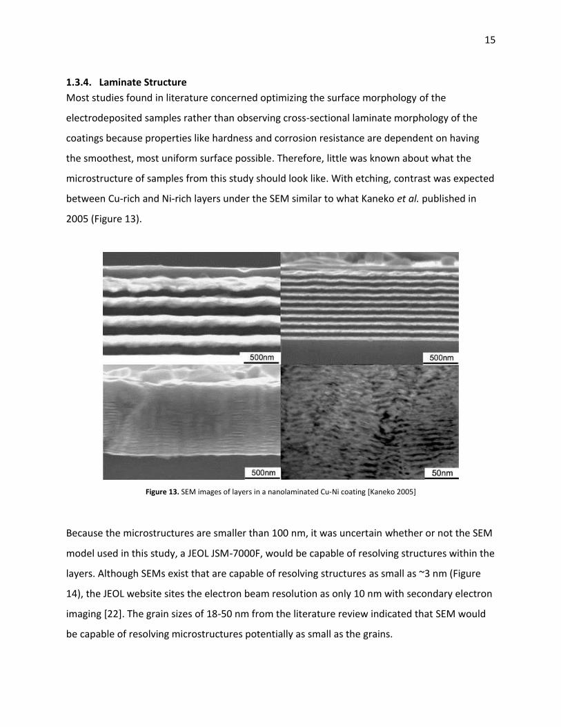
1.3.4. Laminate Structure
Most studies found in literature concerned optimizing the surface morphology of the
electrodeposited samples rather than observing cross-sectional laminate morphology of the
coatings because properties like hardness and corrosion resistance are dependent on having
the smoothest, most uniform surface possible. Therefore, little was known about what the
microstructure of samples from this study should look like. With etching, contrast was expected
between Cu-rich and Ni-rich layers under the SEM similar to what Kaneko et al. published in
2005 (Figure 13).
Figure 13. SEM images of layers in a nanolaminated Cu-Ni coating [Kaneko 2005]
Because the microstructures are smaller than 100 nm, it was uncertain whether or not the SEM
model used in this study, a JEOL JSM-7000F, would be capable of resolving structures within the
layers. Although SEMs exist that are capable of resolving structures as small as ~3 nm (Figure
14), the JEOL website sites the electron beam resolution as only 10 nm with secondary electron
imaging [22]. The grain sizes of 18-50 nm from the literature review indicated that SEM would
be capable of resolving microstructures potentially as small as the grains.

16
Figure 14. Microscopy resolution ranges
Theoretically speaking, the use of sodium saccharin in a Cu-Ni plating bath is effective at
ensuring relatively uniform grains in deposits during pulsed current electrodeposition and is
known to promote the formation of spherical grains (which corresponds to the nodular coating
surfaces that as-deposited samples typically have) [23, 7]. Saccharin-free plating baths tend to
produce more faceted and columnar grains [1, 24] (Figure 15).
Figure 15. SEM images of as-deposited monolithic nanocrystalline Cu-Ni alloys from (left) a saccharin-free plating bath and (right) saccharin-containing bath [Pellicer 2001]

17
2. Materials
All samples were created by Bradford Duvall, a former member of the Flinn research group in
the Materials Science & Engineering department at the University of Washington, in an outside
lab. Monolithic and nanolaminated coatings were deposited polished polycrystalline copper
substrates (1.5 x 1.5 inches / 38 x 38 mm in size; ~14.516 cm2) from a 900 mL plating bath
composed of the following constituents in deionized water: 0.025 M copper sulfate, 0.7 M
nickel sulfamate, 0.25 M sodium citrate, 2.3 g/L sodium saccharin, and 0.15 g/L sodium dodecyl
sulfate (SDS). A spike solution of 0.5 M copper sulfate in deionized water was added periodically
to replace depleted copper in the plating bath. Bath pH was ~4.0. Samples were plated in a
rotating disk electrode set-up with rotation speed maintained at 160 rpm and a direct current
density of 40 mA/cm2 for the monolithic Ni-rich sample. The laminated sample was plated by
pulse current modulated between 40 mA/cm2 for the Ni-rich layers and 10 mA/cm2 for the Cu-
rich layers and rotation speeds of 160 and 500 rpm, respectively. The surface of the
nanolaminated sample had evident swirl marks from the alternation of rotation speeds as
shown in Figure 16.
Figure 16. As-deposited coating surfaces from rotating disk electrode samples (left: monolithic nickel; right: nanolaminate)
Pulse periods in the nanolaminated sample were such that layers of ~100 nm were produced
and plating times for both samples were such that coatings were ~500 μm thick. Part of the
coating thickness in the nanolaminated sample consisted of a Ni-rich top coat ~150 μm thick,
which was intended to help produce a sharp crack in future fracture testing. These two square

18
electrodeposited samples were cut into rectangles for XRD testing as well as several small
beams originally meant for fracture testing.

19
3. Experimental Procedures
3.1. X-ray Diffraction
A Bruker D8 Focus X-ray diffractometer (XRD) with copper-Kα radiation was used at a working
power of 40 kV and 40 mA. The monolithic Ni-rich sample for XRD was 17 x 6 x 1.5 mm in size,
and the nanolaminated XRD sample was 17 x 4.5 x 1.5 mm in size. Each sample was mounted
on a square poly(methyl methacrylate) (PMMA) XRD sample holder with a small amount of clay
to keep the sample level with the top edges of the sample holder. The samples and holders
were oriented such that the X-ray line beam would hit the samples length-wise at the coating
(Figure 17).
Figure 17. Orientation of XRD samples during testing
The swirled surface of the nanolaminated sample was ground smoother with 600 grit
sandpaper to reduce background noise in subsequent XRD spectra and to remove the Ni-rich
top coat that would have interfered with compositional analysis of the nanolaminate. The
sample surfaces were relatively flat, as evident in Figure 18.

20
Figure 18. Nanolaminated and monolithic X-ray diffraction samples
Spectra were collected from 2θhkl between 40 and 80°, with a 1 sec/step collection rate and a
step size of 0.05°. A 0.2 mm divergence slit, 0.6 mm anti-scattering slit, and 0.6 mm
detector/receiving slit were used. All spectral analysis was performed with MDI Jade software
and diffraction spectra database.
3.2. Sample Preparation
All nanolaminate beams were cut with a low-speed diamond saw from the same
electrodeposited sample, but specifically from either a region that experienced lower current
density (toward the center of the square sample) or higher current density (toward the edges of
the square sample where current crowding had occurred) during electrodeposition. Beams
were 8 x 1.5 x 1.5 mm in size. One of each type of beam was restrained by coiled aluminum
clips, oriented so that a beam cross-section would be visible, and the beams were mounted into
the first of three red bakelite pucks with diameters of approximately 31 mm. One of each beam

21
was also mounted, substrate side down, into another red bakelite puck, with a small amount of
black bakelite included along one puck edge for quick sample identification since the samples
were essentially mounted with two-fold symmetry. Small glass squares cut from microscope
slides were inserted into the clips above the beams to hold the clips open more uniformly to
ensure that the beams would lie flat during pressing. This puck was ground with a 240 grit
polishing cloth to an angle of 18.82° so that the angle would reveal elongated grains and layers
(as demonstrated in Figure 19) for easier SEM and EDS analysis.
Figure 19. Diagram showing layer elongation created by angling the surface of the nanolaminated sample "OBL LAM A"
A third puck was created with a single beam of monolithic Ni-rich coating, oriented with the
beam cross section visible. These pucks are shown in Figure 20 in the order that they were
introduced.

22
Figure 20. Orientations of the electrodeposited sample beams mounted in bakelite pucks
From the first puck, the sample positioned at the top will be referred to as “LAM C,” the
nanolaminated sample taken from a high current density region. Below it is “LAM A,” the
nanolaminated sample from a low current density region. The second puck included LAM C on
the left and LAM A on the right, but the LAM C beam became dislodged after polishing so it was
not available for analysis. LAM C on the puck with the oblique surface was aptly named “OBL
LAM C.” The monolithic Ni-rich sample in the third puck was simply named “MONO” during
testing for its monolithic composition.
All samples were initially ground flat on a polishing wheel with 400 grit, 600 grit, and 1200 grit
sandpaper rotating at 300 rpm. Samples were then polished to a glossy finish with the wheel
rotating at 150 rpm and the following order of polishing cloths and alumina polishing media: 9
μm, 3 μm, 1 μm, 0.05 μm, and 0.01 μm. Pucks were sonicated and rinsed in deionized water
before moving on to each successive polishing cloth.
No contrast between copper and nickel layers was visible under SEM (with either secondary
electron imaging or electron backscattering) after just polishing, so various wet etchants were
used to selectively etch either copper or nickel in the coatings. Etchants of varying
concentrations of HCl with and without sonication caused significant pitting when the
nanolaminated samples were immersed for times of five seconds to one minute. The samples

23
were repolished between each etch. Light relief of copper grains and layers was produced in
OBL LAM A by immersing it for five seconds in a solution of 5 mL NH4OH (25-30 wt% ammonia),
5 mL deionized water, and 2 mL fresh 3% H2O2, as recommended by ASM International [25].
Deeper relief of layers was produced in the LAM A and LAM C samples by immersing the puck in
a fresh solution of the same etchant for one minute. The monolithic nickel sample was etched
by immersion for five seconds in a solution of 2 mL HNO3 (68-70 wt%), 1 mL glacial acetic acid
(99.7 wt%), and 1 mL deionized water, as recommended by Smithells Metals Reference Book
for nickel-rich Cu-Ni electrodeposited alloys [26]. All pucks were thoroughly rinsed with
deionized water until the pH of water on top of the pucks was neutral, as read from paper pH
indicator strips. The pucks were then rinsed a final time before drying them under a pressurized
stream of air.
3.3. Scanning Electron Microscopy and Energy Dispersive X-ray Spectroscopy
All samples were placed under house vacuum for at least 24 hours prior to SEM imaging.
Carbon tape was placed across the top of each sample and the sample holder edges to prevent
charging. A JEOL JSM-7000F model field emission scanning electron microscope was used for
secondary electron imaging at accelerating voltages of 10-15 kV.
Quantitative chemical composition data was collected during SEM microscopy by energy
dispersive X-ray spectroscopy (EDS). The spot mode function of EDAX Genesis was used for
layer and microstructure analysis in the nanolaminated samples, but overall compositions were
calculated for the entire computer screen view in the monolithic Ni-rich sample. Accelerating
voltage in the SEM was held at 15 kV for all EDS analysis.

24
4. Results and Discussion
4.1. Laminate Structures from SEM
Initial images on the SEM of the interface between coating and substrate confirmed that the
etchant could produce definition around copper grain boundaries and relief between Cu-rich
and Ni-rich layers.
Figure 21. SEM image of etched polycrystalline copper substrate grains and contrast between coating and substrate

25
Figure 22. Measured and actual layer thicknesses on OBL LAM A under SEM at 20,000X magnification
Figure 23. SEM images of measured layer thicknesses in LAM C at 30,000X magnification

26
Average layer thicknesses were observed to be ~103 nm in both Cu-rich and Ni-rich layers, with
some as small ~70 nm and as large as ~135 nm.
Table 1. Average layer thicknesses and calculated volume fractions of each phase
As such, the volume fractions of Cu-rich and Ni-rich layers were both estimated to be ~0.50.
Because macroscopic swirls were visible on the coating’s surface after electrodeposition,
reflections of this inconsistency were expected to be found within the deposit’s microstructure.
Figure 24. Macroscopic swirls in coating of nanolaminate deposit
Layer inhomogeneity was evident throughout the nanolaminate deposit under SEM. Copper-
rich streaks, non-planar layers, and other defects were present in each nanolaminated sample.

27
Figure 25. Streaks in nanolaminate coating (LAM A sample) at 50X magnification
Figure 26. Optical micrograph of Cu-rich streaks seen across LAM A deposit at 5X magnification
The streaks appeared to be particularly disruptive to the planar orientation of the layers in OBL
LAM A. The white string across the right, bottom corner of Figure 27 is a contaminant.

28
Figure 27. SEM image of OBL LAM A showing streaks in the coating and contrast
Magnifying the view to 1,000X (Figure 28), the streaks appeared to blend into the nanolaminate
layers in the top section, but more abruptly halted the nanolaminate morphology in a step-wise
fashion.

29
Figure 28. SEM image of OBL LAM A showing detailed view of streaks in the coating at 1000X magnification
Non-planar layers also appeared to more randomly-oriented near the substrate than in other
regions of the coating.

30
Figure 29. Non-planar layers in SEM image of OBL LAM A at 2,000X magnification near the substrate
Other layer forms of layer inhomogeneity were evident in an overetched sample that had
undergone fracture testing (LAM A, Figure 30). It was not entirely unclear from this image alone
if the delamination or pitting was an indication of uneven chemical etching or if these
morphologies stemmed from electroplating or fracture testing defects that were merely
enhanced by etching. Region (1) showed delamination across most of the length of beam.
Region (2) showed short-range delamination. Region 3 showed pitting within Region (2).

31
Figure 30. Layer inhomogeneity seen in LAM A under SEM at 1,300X magnification
Examining the area between Regions (2) and (3) further at 10,000X magnification Figure 31, the
layers of the nanolaminate became perceptible. Unlike the region with heavy delamination,
breaks within the layers were clearly visible as well as short lengths of delamination about two
to four μm long. The delamination lines were separated by about 0.5 μm. The layers looked
continuous from the higher region through the lower region. Pits in the lower region appeared
to have a largely round shape, with sizes varying from layer thickness to as many as perhaps 15
or 20 layers.

32
Figure 31. SEM image of LAM A coating showing delamination and regions of pitting at the center of the sample beam at 10,00X magnification
EDS readings were taken of the upper and lower regions to determine the composition around
these peculiar formations. EDS revealed that the upper regions are about 55Ni-45Cu in wt% and
at%, which is consistent with the composition that was predicted at the beginning of this
project and suggests, contrary to the XRD results, that the nanolaminate may not be heavily Ni-
rich. The report revealed that the pitted lower region was surprisingly comprised of nearly 90
wt% Cu, similar to the Cu content calculated for the Cu-rich region an unetched sample from
overall EDS analysis of the bulk nanolaminate deposit. The SEM image clearly showed
nanolamination, so the region was determined not to be a single Cu-rich formation. The

33
increased Cu content did help illuminate why the lower region was so much more severely
attacked by the etchant than the upper region.
4.2. Phase Identification from XRD
Figure 32 shows two distinct peaks in the XRD spectrum for the monolithic Ni-rich sample: the
first at 2-θ = 44.446°, and the second at 51.799°. The peak locations appeared to be consistent
with those of monolithic Cu-Ni deposits from literature, and with the FCC structure of Cu and Ni.
Figure 32. XRD spectrum for monolithic Ni-rich sample
The presence of only two peaks in this range, rather than four distinct peaks corresponding to
typical copper and nickel spectra (two for Cu, two for Ni) or the inclusion of several small
satellite peaks from peak overlapping, indicated the formation of an interstitial solid solution of
the two constituents. This result agrees with the assertion that the sample is a monolithic alloy.
Analysis of the spectrum in Jade showed several possible profile matches, listed in Table 2.
“PDF-#” is the Powder Diffraction File Number. Jade’s exact method of calculating figures of
merit for a profile’s fit to the sample spectrum is unclear, but the lower the figure of merit, the
better the profile’s fit is to the spectrum.

34
Table 2. Phases identified from XRD spectrum for elemental composition of monolithic Ni-rich sample
Although quantitatively, the figures of merit indicated a best fit with the Ni profile, the
(Cu2Ni23)0.16 alloy’s profile appeared to be a better fit qualitatively when seen overlaid on the
sample spectrum in Figure 33. The spiky line is the as-recorded spectrum, the solid outline
around it is the profile fit, and the vertical blue lines indicate a match of peak locations to those
of the diffraction profile.
Figure 33. XRD diffraction profile overlay of (Cu2Ni23)0.16 on the monolithic Ni-rich sample spectrum
Even with this phase chosen, there was a high residual error of fit value of R = 11.26%
(calculated by Jade from weighted background, spectrum, and overlay intensities).
The diffraction spectrum of the nanolaminated Cu-Ni sample shows two distinct peaks in Figure
34 at 44.252° and 51.500°.
Phase Figure of Merit PDF-#
Ni - Nickel 8.8 03-065-2865
(Cu₂Ni₂₃)₀.₁₆ 10.3 01-077-7710
Cu - Copper 100.8 01-070-3038
(CuNi) - Copper Nickel 100.8 01-071-7832
(Cu₁₉Ni)₀.₂ - Copper Nickel 100.8 01-077-7712
Ni - Nickel 100.8 01-089-7129

35
Figure 34. XRD spectrum for nanolaminated sample
The pattern looks nearly identical to that of the monolithic sample – nearly the same peak
locations, complete overlap of Cu and Ni peaks to form distinct peaks without satellites – but
here the peaks’ intensities and widths were slightly different (values listed in Table 4). The ratio
of intensities between the first and second peaks of the monolithic sample was 2.56, whereas
the ratio in the nanolaminated sample is only 1.58, indicating a compositional difference similar
to the one noted in the Baskaran study [16]. In that study, the difference in relative intensity
was observed to decrease with increasing Cu content of their samples, as was assumed to be
the case here. The lack of separate Cu and Ni peaks suggested a metallic solid solution like the
monolithic diffraction spectrum, but such a conclusion would not be accurate because the
nanolaminated sample consists of two unique phases, not one. The XRD beam may not be
precise enough to distinguish the Cu-rich and Ni-phases from each other.
Jade identified two peak profile matches for potential phases: NiCu (dark blue in spectrum) and
Ni (cyan). These both appeared to be a poor qualitative and quantitative fit, with R = 16.1%.
Figure 35. Phases identified from XRD spectrum for elemental composition of the nanolaminated sample
Phase Figure of Merit PDF-#
NiCu - Copper Nickel 12.1 03-065-7246
Ni - Nickel 12.5 03-065-2865

36
4.3. Composition from XRD and EDS
If the monolithic Ni-rich deposit were in fact (Cu2Ni23)0.16, then the composition would be 92Ni-
8Cu by at% or 91.395Ni-8.605Cu by wt%. The average lattice constant from the quantitative
XRD data (Table 3) was 3.5273 Å, which correlates to a Vegard’s law composition of 97.445Ni–
2.555Cu by at% or 97.239Ni–2.761Cu by wt%.
Table 3. Quantitative XRD data for monolithic Ni-rich sample
All data from Table 3 was dependent on the actual diffraction pattern, not on the profile
overlay.
The peak fit for the nanolaminate sample gave a composition of 78.7Ni-21.3Cu by at% or
67.6Ni-32.4Cu by wt%. The average lattice constant was 3.5442 Å (Table 4), which corresponds
to a Vegard’s law composition of 78.7Ni-21.3Cu by at% or 77.5Ni-22.5Cu by wt%.
Table 4. Quantitative XRD data for nanolaminated sample
Using volume fractions calculated from average nanolaminate layer thicknesses in Table 1 and
bulk compositions for the nanolaminate and monolithic Ni-rich deposits calculated from
Vegard’s Law or the diffraction peak fit, the Cu content of Cu-rich layers was found to be 42.5
Peak # 2-θ (°)
d (Å),
lattice plane
spacing
Height
(electron
counts)
Area
Relative
Intensity
(%)
Full Width
Half Max
Crystallite
Size (nm)
Miller
Indices
(h k l)
Lattice
Constant
(Å)
1 44.446 2.0367 1583 769.6 100.0 0.490 19 1 1 1 3.5276
2 51.799 1.7635 617 322.7 39.0 0.686 13 2 0 0 3.5270
Peak
#2-θ (°)
d (Å),
lattice plane
spacing
Height
(electron
counts)
Area
Relative
Intensity
(%)
Full Width
Half Max
Crystallite
Size (nm)
Miller
Indices
(h k l)
Lattice
Constant
(Å)
1 44.252 2.0452 1327 589.9 100.0 0.436 22.3 1 1 1 3.5423
2 51.500 1.7731 838 467.9 63.1 0.604 15.8 2 0 0 3.5461

37
wt% and 56.6 wt% Cu, respectively. Both values are far lower than the EDS value of 91.6 wt%
Cu. The copper content measured by EDS is thought to be more accurate because the Cu-rich
layers etched very easily compared to the Ni-rich ones when the nanolaminate samples were
treated with a solution that preferentially attacks Cu. Cu-rich layers were also deposited with
plating parameters known to create highly Cu-rich deposits, so the low Cu-content indicated by
the XRD values do not seem like reasonable estimates. The discrepancy may be stem from the
XRD’s inability to distinguish a Cu-rich phase in the nanolaminated sample.
Table 5. Copper content of Cu-rich layers from EDS analysis and calculated from XRD data
EDS analysis was also performed on the etched monolithic Ni-rich sample to provide another
reference for the actual Cu content of the Ni-rich layers. The composition of the overall MONO
coating was found to be 70.91 at% Ni – 29.09 at% Cu, or 69.25 wt% Ni – 30.75 wt% Cu. These
differ significantly from the composition values collected from XRD and are closer to the EDS
values collected from the unetched samples from previous research. The discrepancy between
EDS compositions may be a result of the etching; a strong etchant that preferentially reacts
with Ni was used to create definition of microstructures and grains in the alloy. With Ni
removed disproportionately with the Cu in the monolithic sample, the Ni content was reduced
relative to the Cu content. With this in mind, the 91.6 wt% Cu value again appears to be more
plausible than ~40-57 wt% Cu from XRD.

38
4.4. Grain Sizes from XRD and SEM
Full width half max values of the nanolaminate from XRD were lower than those of the
monolithic sample, yielding calculated grain sizes of 22.3 nm and 15.8 nm. The average grain
size was therefore 19.1 nm, compared to just 16.0 nm for the monolithic Ni-rich sample. The
nanolaminate grain sizes agree with the ~18-50 nm size range from the literature review, but
the average grain size of the monolithic sample is much smaller than the 29 nm size reported in
literature. It is important to note, though, that the samples in this study were electrodeposited
on a rotating disk electrode, whereas the literature studies used static plating baths with
agitation from a magnetic stir bar instead. Rotating the substrate during plating increases mass
transport of the Cu and Ni ions from the bath to the substrate, increasing the deposition rate as
well. With less time to take on a preferred orientation, the grains may be limited to a smaller
size. This theory may not be entirely valid, though, because if that were the case, a smaller
grain size would have been evident in the nanolaminated sample since speed was increased
during deposition of Cu-rich layers. It is more reasonable to assert that because the studies of
monolithic samples from literature did not use a grain-refining agent in the plating bath,
faceted grains grew rather than the more spherical ones that are common with sodium
saccharin addition. With grains approximately the same volume, a faceted or columnar grain
would appear to be larger in the XRD spectra than a more uniform or spherical grain.
Considering that a spike solution was used in the plating bath in this study to replenish the
copper supply, it also seems plausible that the nanolaminated sample was plated either after
the addition of a spike solution or after several plating runs in the same bath; decreases in
saccharin concentration are known to yield larger grains in Ni-based deposits than with
saccharin additions [23]. Sodium saccharin did appear to produce a consistent range of grain
sizes in both monolithic and nanolaminated samples in this study. There was a difference of
~30.0% between the largest and smallest detected grain sizes from XRD in each type of deposit.
Under SEM, the coating had a somewhat nodular consistency, with nodes appearing to be
about 20-30 nm in diameter in Figure 36. Nodular growths were expected because the
presence of saccharin in plating baths has been known to produce spherical grains in

39
electrodeposited nickel thin films [23]. These sizes are not consistent with the grain sizes
calculated from XRD, so these structures and the overall texture may merely be relief due to
contact with a highly corrosive etchant. Cu-Ni nanolaminates have been known to exhibit grain
clustering in a colony-like morphology [2], so the pits may be nodular/spherical grain clusters
that were etched out between smooth, polished regions where grains remained. The fact that
these round pits are seen close to the substrate and faceted notches were observed far from
the substrate may be an indication that the plating bath was becoming depleted of saccharin
content. Unfortunately no images could be focused at a magnification greater than 60,000X
(notice that the scale bar is only 100 nm long), so no grains were distinguishable. The coating
appeared to be uniformly textured, similar to those observed by Pellicer et al [1].
Figure 36. SEM image of monolithic Ni-rich coating showing spongy-like texture of round protrusions and pits at 60,000x
magnification
A similar texture and more spherical pits were seen in the Ni-rich top coat of the nanolaminated
deposit after the Cu etching.

40
Figure 37. Spherical pits and uniform texture observed in Ni-rich top coat of OBL LAM A under SEM at 10,000X magnification
This pattern was also evident in heavily delaminated areas of LAM A after overetching Cu-rich
regions. The pit sizes ranged from 33.8-78.8 nm.
Figure 38. SEM image of LAM A near substrate showing round pits at 50,000X magnification

41
Pit sizes ranged between ~40 and 65 nm in OBL LAM A in the sides of the Ni-rich layers where
Cu-rich layers had been etched out. The spherical shape of the recessed pits again supports the
notion that the grains may have formed large round grain colonies from saccharin addition to
the bath.
Figure 39. SEM image of round pits between etched layers of OBL LAM A

42
5. Conclusions Significant contributions have been made to the current study of structure-processing-property
relationships of the Cu-Ni nanolaminate system. Nanolaminated samples exhibited a non-
uniform microstructure, though possible grain structure in the form of grain colonies was
successfully observed despite the lack of SEM capability to resolve the ~20 nm grains. Laminate
structure was also characterized, with regions of planar and non-planar layers evident
throughout the nanolaminate deposit. Non-planar layers were most prevalent near the
substrate and adjacent to large Cu-rich streaks seen in the coating. These and other defects
indicate that the increase in rotation speed during Cu-rich deposition is detrimental to the
homogeneity of layer formation. Phase compositions of the Cu-rich and Ni-rich layers were
inconclusive because of disparity between XRD and EDS data, though the EDS estimates of 91.6
wt% Cu in Cu-rich and 19.0 wt% Cu in Ni-rich is thought to be more accurate since the XRD had
difficulty identifying distinct phases within the nanolaminate and ease of etching suggested
high copper content within Cu-rich layers. These conclusions provide a better understanding of
the fracture behavior of Cu-Ni nanolaminates as it relates to processing (unique to rotating disk
electrode deposition) and structural properties. They provide a guide for future processing and
characterization of future electrodeposited Cu-Ni nanolaminate samples.

43
6. Future Work Refinement of the etching process is recommended to yield more consistent layer definition
and potential grain structure within laminates. Difficulty with phase identification in XRD might
also be alleviated with the use of equipment better suited for nanocharacterization of
nanolaminate phases in solid samples rather than merely powdered samples (i.e. diffraction
peak profiles for solid samples if XRD).
TEM imaging may also be better suited to resolve the nanocrystalline grains, though it would
not provide valuable information until more uniform nanolaminate deposits are produced. AFM
imaging may provide valuable structural information as well.

44
References
[1] E. Pellicer, A. Varea, S. Pane, K. M. Sivaraman, B. J. Nelson, S. Surinach, M. D. Baro and J.
Sort, "A comparison between fine-grained and nanocrystalline electrodeposited Cu-Ni
films. Insights on mechanical and corrosion performance," Surf Coat Tech, vol. 205, pp.
5285-5293, 2011.
[2] M. Agarwal, V. Kumar, S. Malladi, R. Balasubramaniam and K. Balani, "Effect of current
density on the pulsed co-electrodeposition of nanocrystalline nickel-copper alloys," JOM,
vol. 62, no. 6, pp. 88-92, 2010.
[3] V. F. Lins, E. S. Cecconello and T. Matencio, "Effect of the Current Density on Morphology,
Porosity, and Tribological Properties of Electrodeposited Nickel on Copper," J. Mater. Eng.
Perform., vol. 17, no. 5, pp. 741-745, 2007.
[4] Y. Kaneko, Y. Mizuta, Y. Nishijima and S. Hashimoto, "Vickers hardness and deformation of
Ni/Cu nano-multilayers electrodeposited on copper substrates," J Mat Sci, vol. 40, pp.
3231-3236, 2005.
[5] N. Rajasekaran and S. Mohan, "Structure, microstructure and corrosion properties of
brush-plated Cu-Ni alloy," J Appl Electrochem, vol. 39, pp. 1911-1916, 2009.
[6] G. S. Was and T. Foecke, "Deformation and fracture in microlaminates," Thin Solid Films,
vol. 286, pp. 1-31, 1996.
[7] S. K. Ghosh, A. K. Grover, G. K. Dey and M. K. Totlani, "Nanocrystalline Ni-Cu alloy plating
by pulse electrolysis," Surf Coat Tech, vol. 126, pp. 48-63, 2000.
[8] Modumetal, LLC., "Corrosion," [Online]. Available: http://modumetal.com/corrosion.php.
[Accessed 28 November 2012].
[9] G. S. Rohrer, Models for predicting phase stability, Cambridge: Cambridge University,
2001, pp. 425-426.
[10] S. K. Ghosh, A. K. Grover, G. K. Dey, U. D. Kulkarni, R. O. Dusane, A. K. Suri and S. Banerjee,
"Structural characterization of electrodeposited nanophase Ni-Cu alloys," J Mater Res, vol.
21, no. 1, pp. 45-61, 2006.
[11] M. de los A. Cangiano, M. W. Ojeda, A. C. Carreras, J. A. Gonzalez and M. del C. Ruiz, "A
study of the composition and microstructure of nanodispersed Cu-Ni alloys obtained by
different routes from copper and nickel oxides," Mater Charact, vol. 61, pp. 1135-1146,
2010.
[12] S. K. Ghosh, G. K. Dey, R. O. Dusane and A. K. Grover, "Improved pitting corrosion
behaviour of electrodeposited nanocrystalline Ni-Cu alloys in 3.0wt.% NaCl solution," J
Alloy Compd, vol. 426, pp. 235-243, 2006.

45
[13] G. Abadias, A. Michel, C. Tromas, C. Jaouen and S. N. Dub, "Stress, interfacial effects and
mechanical properties of nanoscale multilayered coatings," Surf Coat Tech, vol. 202, pp.
844-853, 2007.
[14] E. Pellicer, A. Varea, K. M. Sivaraman, S. Pane, S. Surinach, M. D. Baro, J. Nogues, B. J.
Nelson and J. Sort, "Grain boundary segregation and interdiffusion effects in the nickel-
copper alloys: an effective means to improve the thermal stability of nanocrystalline
nickel," ACS Appl. Mater. Interfaces, vol. 3, pp. 2265-2274, 2011.
[15] B. D. Cullity and S. R. Stock, Crystallite Size, Upper Saddle River: Prentice Hall, 2001, pp.
167-171.
[16] I. Baskaran, T. S. Narayanan and A. Stephen, "Pulsed electrodeposition of nanocrystalline
Cu-Ni alloy films and evaluation of their characteristic properties," Mater Lett, vol. 60, pp.
1990-1995, 2006.
[17] B. D. Cullity and S. R. Stock, "Crystallite Size," in Elements of X-Ray Diffraction, Upper
Saddle River, Prentice Hall, 2001, pp. 167-171.
[18] N. Rajasekaran and S. Mohan, "Preparation, corrosion and structural properties of Cu-Ni
multilayers from sulphate/citrate bath," Corros Sci, vol. 51, pp. 2139-2143, 2009.
[19] L. Bonou, Y. Massiani and J. Crousier, "Electrodeposition and corrosion behavior of copper-
nickel alloys," Brit. Corros. J., vol. 29, no. 3, pp. 201-205, 1994.
[20] F. Ebrahimi and A. J. Liscano, "Microstructure/mechanical properties relationship in
electrodeposited Ni/Cu nanolaminates," Mat Sci Eng A-Struct, vol. 301, pp. 23-34, 2001.
[21] NDT Resource Center, "X-Ray Generators," [Online]. Available: http://www.ndt-
ed.org/EducationResources/CommunityCollege/Radiography/EquipmentMaterials/xrayGe
nerators.htm. [Accessed 1 June 2012].
[22] JEOL, "JSM-7000F Optimized Specimen Chamber Geometry," 2006-2012. [Online].
Available:
http://www.jeol.com/RESOURCES/ProductPresentations/JSM7000FOptimizedSpecimenCh
amberGeometry/tabid/355/Default.aspx. [Accessed 1 June 2012].
[23] A. C. Mishra, A. K. Thakur and V. Srinivas, "Effect of deposition parameters on
microstructure of electrodeposited nickel thin films," J. Mater. Sci, vol. 44, pp. 3520-3527,
2009.
[24] C. Bonhote and D. Landolt, "Microstructure of Ni-Cu multilayers electrodeposited from
citrate electrolyte," Electrochimica Acta, vol. 42, no. 15, pp. 2407-2417, 1997.
[25] ASM International, "Metallurgy and Microstructures," ASM Handbook Volume 9, p. 778,
2004.
[26] W. F. Gale and T. C. Totemeir, Smitells Metals Reference Book, 8th ed., Elsevier

46
Butterworth-Heinemann, 2004, p. 995.