Embed Size (px)
Citation preview

Copyright © 1994, by the author(s).
All rights reserved.
Permission to make digital or hard copies of all or part of this work for personal or
classroom use is granted without fee provided that copies are not made or distributed
for profit or commercial advantage and that copies bear this notice and the full citation
on the first page. To copy otherwise, to republish, to post on servers or to redistribute to
lists, requires prior specific permission.

LOW-POWER CMOS LIBRARY DESIGN
METHODOLOGY
by
Tom Burd
Memorandum No. UCB/ERL M94/89
4 November 1994

LOW-POWER CMOS LIBRARY DESIGN
METHODOLOGY
by
Tom Burd
Memorandum No. UCB/ERL M94/89
4 November 1994
ELECTRONICS RESEARCH LABORATORY
College of EngineeringUniversity of California, Berkeley
94720

Low-Power CMOS Library DesignMethodology
by
Tom Burd
Master of Science in Electrical Engineeringand Computer Science
University of California, Berkeley
ABSTRACT
The emphasis in VLSI design has shifted from high speed to low power due to the
proliferation of portable electronic systems. The goal of this project is to develop amethodology for designing low power circuits and cells, and to implement this method
ology in constructing a general purpose cell library that can be used to design low
power integrated circuits. The design methodology encompasses all aspects of circuit
design; it optimizes transistor size, logic style, layout style, cell topology, and circuitdesign for low power operation. The cell library is implemented within the framework
of the LagerlV CAD suite for rapid logic synthesis and layout generation. Several chipsdesigned with the low power library demonstrate the power reduction that can be
achieved. The entire cell library is characterized to determine typical delay, averagepower dissipation, and area for each cell so the IC designer can make reasonable speed,
area, and power estimations while still in the architecture design stage.

Acknowledgments
First, I would like to thank my research advisor Professor Bob Broderson for
his support and guidance of this research. And most importantly, it is because of him
and a few others that I am at Berkeley doing this research, and not elsewhere 3000
miles away. Also, I would like to thank Professor Jan Rabaey for his significant
contribution to and guidance of the low power digital design effort here at Berkeley.
I would like to thank the people who contributed their time to designing cells
for the library: Andy Burstein, who designed the SRAM cell, and is currently designing
the ROM and PLA cells. Renu Mehra, who designed the dpp register file. Scarlett Wu,
who designed the dpp shifter cells, and the logics cell. Lastly, Sam Sheng, who
designed the log comparator cell, and who tells me he will get around to writing the
docs for it "soon".
I would also like to thank Brian Richards for all his help with Lager-related
issues, Anantha "The Godfather of Low-Power" Chandrakasan for his valuable input on
low-power design, and Mani Srivastava for his help with dpp.
I want to thank all the remaining members of BJgroup for their help and input
on this research as well as other matters.
Lastly, and most importantly, I would like to thank Joyce, the love of my life,
for giving me boundless personal support, for being a continual source of motivation,
and for enduring my crazy work schedule. To her I dedicate this work.
This work was supported under the ARPA Grant J-FBI-93-153.

Contents
Table of Contents iii
List of Figures v
List of Tables vi
1 Introduction 1
2 Power Dissipation in CMOS ICs 42.1 Sources of Power Dissipation 4
2.1.1 Dynamic Switching Power 52.1.2 Short-Circuit Current Power 6
2.1. 3 Leakage Current Power 8
2.1.4 Static Biasing Power 10
2.2 Process Modificationsfor Reducing Power 112.2.1 Optimizing VT 112.2.2 Process Scaling 12
2.2. 3 Fabrication Advancements 12
3 Circuit Design Methodology 143.1 Voltage reduction 14
3.1.1 Power Supply 15
3.1.2 Signal Swing 17
3.2 Capacitance Reduction 21
3.2.1 Physical Capacitance 213.2.1.1 Transistor Sizing 223.2.1.2 TSPC Clocking Methodology 233.2.1.3 Efficient Layout 24
3.2.2 Switching Frequency 253.2.2.1 Logic Style 263.2.2.2 Self-timing 28
3.3 Minimizing Other Power Components 283. 3.1 Short-circuit Current Power 29
3. 3.2 Static CurrentPower 31
4 Cell Libraries 32
ui

4.1 Standard Cell Library (stdcell2_31p) 324.1.1 LayoutFormat 33
4.1.2 Implementation 35
4.2 DPP Cell Library (dpplp) 354.2.1 LayoutFormat 36
4.2.2 Implementation 37
4.3 TimLager Cell Library (timlagerlp) 384. 3.1 LayoutFormat 404. 3.2 Implementation 40
4.4 1.2 urn Pad Cell Library (padl_21p) 414.4.1 LayoutFormat 434.4.2 Implementation 44
4.5 Characterization Process 44
4.6 User Design Considerations 46
4. 6.1 Using TSPC registers and FIFOs 464. 6.2 Clock skew 47
4. 6. 3 Fan-out limitations 47
5 Results 49
5.1 SPICE Model Calibration 49
5.2 Improvements over Existing Libraries 515.2.1 Standard Cell Library 525.2.2 DPP Cell Library 555.2. 3 TimLager Cell Library 57
5.3 ICs Implemented with the Low Power Library 585.3.1 Low Power 64k SRAM Chip 595. 3.2 Protocol Chip 60
5. 3.3 "Video Decompression Chip Set 61
6 Conclusions 62
6.1 Summary 62
6.2 Future Work 63
A Complete Cell Library Listing 64A.l Standard Cell Library 68
A.2 Datapath Cell Library 72
A.3 TimLager Cell Library 74
A.4 CMOS 1.2um Pad Cell Library 76
References 77
IV

List of Figures
1.1 Hierarchical Design Space of Electronic Systems 2
2.1 Dynamic Switching PowerDissipation; Sources of Capacitance 52.2 Short-circuit Energy Versus Input Rise/fall Time 72.3 IDvs. VDS for MOSFET in Subthreshold Region 92.4 Implementing Complex Logic with Static Biasing (pseudo-NMOS) 10
3.1 Normalized Delay Versus Supply Voltage 163.2 Level Clamp to Reduce Signal Swing 183.3 Signal Amplification / Swing Reduction in Memory Circuits 203.4 Schematic of TSPC Style Register 243.5 PDP of Various Logic Styles for an 8-bit Adder, for Varying Vdd 27
4.1 Layout Format for Standard Cell Library 344.2 Layout Format for the Data-path LibraryCells 374.3 Layout format for the TimLager Library 404.4 Level Converting Pad 424.5 Layout Format for 1.2|im Pad Library 43
5.1 Test Setup for Measuring Delay and Power of an Adder Cell 50
5.2 Block Diagram of 32-bitDatapath Implemented in Example#3 555.3 Block Diagram of 32-bit Datapath Implemented in Example #4 56

List of Tables
5.1 Comparison of Measured and Simulated DelayandEffective Capacitance ... 515.2 Example #1: Integer Pipeline Controller and Instruction Decoder 535.3 Example #2: Cache Tag Valid Bit Detector 545.4 Example #3: A Simple Datapath 555.5 Example #4: A Complex Datapath 565.6 Example #5: A 32 x 32 FIFO 575.7 Example#6: A 128 x 32 FIFO 585.8 Statistics for the 64k Low Power SRAM chip 605.9 Statistics for the ProtocolChip 605.10 Statistics for the Video Decompression Chip Set 61
A.1 Standard Cell Library 68A.2 Datapath Library 72A.3.1 FIFO Cell 74A.3.2 SRAM Cell 75A.4 CMOS 1.2um PadLibrary 76
VI

Introduction1
With the explosive growth in the portable electronics market in the last few
years, the emphasis in VLSI and system design is shifting away from high speed to low
power. However, devices such as PDAs (Personal Digital Assistants) and notebook
computers still require a large amount of data processing/throughput. For multimedia
devices, like the PDA, the predominant goal of low-power design is to minimize total
power dissipation of the system given some fixed data throughput requirements
[chan92]. With portable computing, low-power design requires system design that
balances the speed and power constraints.
Many portable systems, such as notebook computers, have their power
dissipation dominated by I/O devices — primarily disk drives and LCD displays — so
that reducing the power of the internal CPU and other ICs, does not yield much savings
in total power dissipation. The InfoPad multimedia wireless-terminal project [chan93]
(which spawned this library design project), however, attempts to minimize power in all
aspects of design, such that using commercial ICs would make them dominate the total
power dissipation of the portable pad. This system demands total power of the ICs to be
well under lOOmW, while commercial ICs would dissipate several Watts.
In order to minimize the power of these ICs, a low-power methodology was
developed that spans from process-level technology modifications all the way up to

high-level system design [chan92]. The diagram in Figure 1.1 depicts the five layers of
design space across this span. The designer can make optimizations at all levels of the
design space, which have a cumulative effect on total system power reduction. Other
work has concentrated on architecture, algorithm, and system-level (printed circuit
board, multiple ICs, and monolithic IC) power minimization [chan93]. The process
technology is the only level that the designer has limited control over.
The low-power library design methodology, developed here in this thesis,
predominantly encompasses the area of circuit design, with some extensions upwards
into architecture design —when determining the optimal adder topology —and some
implications on the underlying process technology - such as what the optimal VT for
minimizing power is. Of course, using the library does not guarantee a low-power
design. The library must be used in conjunction with higher-level optimizations to yield
a global power minimization.
System Design
Algorithms
Architecture Design
Circuit Design
Process Technology}Design space encompassed by low-
power library design methodology.
FIGURE 1.1: Hierarchical Design Space of Electronic Systems.
The cell library implemented in this work is designed with the MOSIS SCMOS
design rules [ayres88]. These rules allow for two metal layers and any combination of
wells: nwell, pwell, and twin-tub. The library cells were designed for, and fully
compatible with, the LagerlV CAD tool design suite [brod92].

This thesis contains 5 chapters. Chapter 2 analyzes the sources of power
dissipation in CMOS ICs. The circuit design methodology developed for this library is
described in Chapter 3. Next, Chapter 4 details the cell library - library-specific design
issues, layout formats, and a summary of its implementation. Also described are some
of the user design considerations of using the library. Chapter 5 provides measured
results from test chips using the library, and a look at the power and area improvement
of this library over previously used ones. Lastly, Chapter 6 summarizes the work herein
and looks at future directions. The subsequent appendices provide a full library listing,
along with speed and power numbers of the cells.
Power Dissipationin CMOS ICs
2
Unlike bipolar technologies, where a majority of power dissipation is static,
the bulk of power dissipation in properly-designed CMOS circuits is the dynamic
charging and discharging of capacitances. Thus, a majority of the low power design
methodology is dedicated to reducing this predominant factor of power dissipation.
However, there are also other components of power dissipation in CMOS
circuits as described in the following section. Most of them are negligible, but one
component that can become significant in poorly-designed circuits is power dissipated
by short-circuit currents. The magnitude of this component is determined by the design
methodology used.
Section 2.2 discusses process modificications that can be made to reduce
power dissipation. While process design is beyond the control of the circuit designer, it
is important to understand what the impact of future process generations has on power
dissipation.
2.1 Sources of Power Dissipation
There are four main source of power dissipation: dynamic switching power due
to the charging and discharging circuit capacitances, leakage current power from

reverse-biased diodes and subthreshold conduction, short-circuit current power due to
finite signal rise/fall times, and static biasing power found in some types of logic styles
(i.e. pseudo-NMOS).
2.1.1 Dynamic Switching Power
When CMOS circuits switch, the output is either charged up to VDd» or
discharged down to ground. In static logic design, the output only transitions on an
input transition, while in dynamic logic, the output is precharged during half the clock
cycle, and transitions can only occur in the second clock phase, depending upon the
input values. In both cases, the power dissipated during switching is proportional to the
capacitive load; however, they have different transition frequencies.
For the simple inverter gate shown in Figure 2.1, it can be shown that a low-to-
high output transition draws ClVdd2 Joules (energy) from the power supply, VDD
[chan94]. The high-to-low output transition dissipates the energy stored on the
capacitor into the NMOS device. Given a frequency/of low-to-high output transitions,
the power drawn from the supply is CLVDD2/. This simple equation holds for more
complex gates, and other logic styles as well, given a periodic input.
VddVdd
rO\ .
Jdd
1
E = CLVDI/
v„
J~'out
X
i—01
c
if~4bp
Voat
—J—Qbn
_tT~& cL=lc,'O
^-kFIGURE 2.1: Dynamic Switching Power Dissipation; Sources of Capacitance.
Accurate calculations for Cl can be done. The basic capacitor elements are
shown in Figure 2.1. The net loading capacitance, Cl, consists of gate capacitance of

subsequent gate inputs attached to the inverter output, interconnect capacitance, and the
diffusion capacitance on the drains of the inverter transistors. Test chips have shown
that for 1.2u,m ICs, the total capacitance is split roughly equally between these three
types. As the minimum gate length scales down, though, interconnect capacitance will
become dominant.
Usually, the value of/is a difficult number to quantify, as it is most likely not
periodic, and is correlated with the input test vectors into the circuit. Without doing a
switched-level circuit simulation, the best way to calculate/ is to perform statistical
analysis on the circuit to determine a mean value [land93].
Since dynamic switching power is the major component of overall power
dissipation, the low-power design methodology concentrates on minimizing total
capacitance, supply voltage, and frequency of transitions.
2.1.2 Short-Circuit Current Power
Short circuit currents occur when the rise/fall time at the input of a gate is
larger than the output rise/fall time. For the ideal case of a step input, the transistors
change state immediately, one turning on, one turning off. There is not a conductive
path from the supply to ground. For real circuits, however, the input signal will have
some finite rise/fall time. While the condition VTn < Vin <VDD - IVTpl holds for the
input voltage, there will be a conductive path open because both devices are on.
The longer the input rise/fall time, the longer the short-circuit current will
continue to flow, and the average short-circuit current increases. Figure 2.2 plots the
ratio of energy consumed by short-circuit current versus the ratio of input rise/fall time
to output rise/fall time. The AE increases dramatically with increasing input rise/fall
time. To minimize the total average short-circuit current power, it is desirable to have
equal input and output edge times. While the graph indicates a ratio of zero is the most

desirable, since the input rise/fall time is the output rise/fall time of another gate this is
not the case. While the second gate has zero extra power dissipation, the first one will
have a significant increase due to the fast output rise/fall time.
AE/E(tRin=0)
VDD= 5V
Pevipe Sizes;W/LIP= 7.2nm/1.2umW/LIN = 2.4um/1.2um
Vnn=3.3V
4r-•'*«/'*<FIGURE 22: Short-circuit Energy Versus Input Rise/fall Time, (statue CMOS inverter)
The peak magnitude of the short-circuit current is dependent on device size.
The average current, however, is roughly independent of device size for a fixed load
capacitance. While the peak magnitude of the current increases, the rise/fall time
decreases so that the average current is the same. If all devices are sized up so that the
load capacitance scale up proportionally, then the rise/fall time remains constant and
the average current (and power) scales up linearly with device size.
Short-circuit current power is either linearly or quadraticly dependent on the
supply voltage, depending on the size of the channel length. While reducing the supply
increases the duration of the current linearly due to increased rise/fall times, the peak
magnitude of the current is reduced linearly (velocity saturation), such that the average
current is approximately constant, and the average power is just a linear function of
supply voltage (P=IV). For larger devices that are not velocity saturated, the average
current is approximately linear with supply voltage so that the average power is a
quadratic function of supply voltage.
For most ICs, the short-circuit power dissipated is approximately 5-10% of the
total dynamic power [veen84]. If the supply is lowered to below the sum of the

thresholds of the transistors, VDD <VTn +IVTpl, however, short-circuit currents will be
eliminated because both devices cannot be on at the same time for all values of input
voltage.
2.1.3 Leakage Current Power
There are two types of leakage currents: reverse-bias diode leakage on the
transistor drains, and sub-threshold leakage through the channel of an "off* device. The
magnitude of these currents is set predominantly by the processing technology;
however, there are some things that a designer can do to minimize their contribution.
The diode leakage occurs when a transistor is turned off, and another active
transistor charges up/down the drain with respect to the former's bulk potential. In the
case of the inverter with a high input voltage, the output voltage will be low because the
NMOS transistor is on. The PMOS transistor will be turned off, but its drain-to-bulk
voltage will be equal to the supply voltage, -VDD. The resulting diode leakage current
will be approximately IL = ADJs» where AD is the area of the drain diffusion, and Js is
the leakage current density, set by the technology. For the MOSIS 1.2ujn technology, Js
is approximately l-5pA/u,m2 (25° C), and the minimum AD is 7.2|xm. Since the diode
reaches maximum reverse bias current for relatively small reverse bias potential, the
leakage current is roughly independent of supply voltage. It is proportional to diffusion
area and perimeter, however, so it is desired to minimize the diffusion area and
perimeter in the layout. The leakage current density is temperature sensitive, as well, so
Js can increase dramatically at higher temperatures.
For a 1 million transistor chip, there are an equal amount of drain diffusions,
but only 1 out of 2 has leakage. Assuming the average area of a drain is 10um2, then the
average total leakage current is 25u,A. Thus, the power dissipated is below lOOuW. For
chips with a power dissipation greater than lOmW, the leakage contributes less than

1%. However, for low-power ICs in the lmW range, this component can become a
significant fraction.
Subthreshold leakage occurs under similar conditions as the diode leakage. In
the inverter described above, the PMOS was turned off, but even for VGS = OV, there is
still current flowing in the channel due to the VDS potential of -Vdd- The Id vs. Vds
characteristic, as shown in Figure 2.3, has an exponential relation in the subthreshold
region (Vqs < IVfl), and the subthreshold current magnitude occurs at Vqs = OV for a
high input voltage.
Id' %Subthreshold Saturatedjq-3 _ Region Region
I Decreasing VDs» VDd
FIGURE 13: IDvs. VDS for MOSFET in Subthreshold Region.
The magnitude of the subthreshold current is both a function of process, device
sizing, and supply voltage [sze81]. The process parameter that predominantly affects
the current value is Vj. Reducing V^ exponentially increases the subthreshold current.
For the MOSIS process, VT is 0.7V - 0.9V, and the current magnitude for a ranges from
500fA - lOpA, which is similar in magnitude to diode leakage current. For every
transistor with diode leakage, the same bias conditions are present for subthreshold
leakage, such that the total power dissipation of the two are roughly the same
magnitude.
The subthreshold current is also proportional to the transistor device size
(W/L), and an exponential function of the supply voltage. Thus, the current can be
minimized by reducing the transistor sizes, and by reducing the supply voltage.

10
2.1.4 Static Biasing Power
While most static biasing was removed from MOS ICs during the switch from
NMOS to CMOS, there are still some circuits where static biasing can be beneficial in
reducing the total power, as will be shown below. There is usually a large area savings
as well. This is primarily applicable for higher-frequency circuits, where the savings of
dynamic power is proportionally higher. For circuits below 10-100 kHz, adding static
loads will usually increase the total power. Also, the applicable circuits are usually
asynchronous, where dynamic precharging methods cannot be used.
Only in complex logic functions do static loads prove to be useful in providing
a power savings. In Figure 2.4 is an example gate ~ it is a wide AND-OR-Invert gate.
To implement this in full static CMOS would require several times the area to
implement the stacked PMOS transistors. The extra PMOS transistors would also
increases the capacitance on the input nodes, which would load down the previous
gates. Since the desired output is asynchronous, it cannot be implemented with a
dynamic logic style.
Vnp
A1B1+A2B2—-+ANBN
O
FIGURE 2.4: Implementing Complex Logic withStatic Biasing (pseudo-NMOS).

11
2.2 Process Modifications for Reducing Power
Several process modifications can be made to reduce power in CMOS ICs.
Most of these are occurring with each new process generation — reducing minimum
gate lengths, adding metal layers, etc. The one parameter that has not changed is the
device thresholds. Unfortunately, the circuit designer does not have control over the
process parameters, and must work with the given process. Because of this, process
modifications is not part of low-power circuit design methodology; however, it is
important to understand how process modifications can reduce power so that future
processes can be optimized for low-power IC circuits.
2.2.1 Optimizing VT
Until recently, the VT in most CMOS processes has been set to a fairly high
potential — 0.7V to l.OV. For 5V circuit operation, this has little impact on circuit
delay, which is inversely proportional to (VDd - VT)2. The main benefit for such a large
threshold is that the subthreshold leakage is reduced exponentially. While the total
leakage current of an IC is still well below the average supply current under operation,
the reduced subthreshold current prolongs the duration of stored charge in dynamic
circuits, providing more robust operation (due to longer leakage times). Thus, there has
been little reason to reduce the thresholds until recently, with the decrease of supply
voltages to 3.3V, and the emphasis on low-power design.
Reducing VT enables the supply voltage to be dropped as well. This maintains
circuit speed, but results in a corresponding power decrease. However, the limitation on
this is that at low thresholds, the subthreshold currents become a significant, if not
dominant, portion of the average current drawn from the supply. Previous work has
shown the optimal VT to range from 0.3V [chan92] down to below 0.1V [liu93]
depending on the conditions of circuit operation.

12
2.2.2 Process Scaling
With every new process generation, all of the lateral, and some of the vertical
dimensions are scaled down. This has an immediate impact on reducing power
dissipation, as well as increasing circuit speed. The primary effect of process scaling is
to reduce all the capacitances, which provides a proportional decrease in power and
circuit delays. Device sizes can be reduced to keep delay constant over process scaling,
which will yield an even larger power dissipation reduction.
Both gate capacitance and interconnect capacitance can be expressed as
C = WLEoxCl/tox). The width (W), length (L), and oxide thickness (tox) all scale
roughly equally by a factor s, so the total capacitance scales down by the same factor s.
Diffusion capacitance is a more complex function of process scaling, but is reduced by
a factor between s and S3f2. For a constant supply voltage, both the power and circuit
delays scale down approximately by the factor s. Thus, power reduction is
accomplished with no alterations in the circuit design.
As mentioned earlier, not all the vertical dimensions scale down. In particular,
the thickness of the interconnect metal is roughly the same across processes, due to
fundamental processing requirements [bako90]. This increases the fringe capacitance
from the side of the metal to the substrate, and increases the capacitance between
adjacent interconnect segments. With these secondary effects considered, the overall
capacitance scaling is somewhat below a factor s, and is difficult to accurately
characterize without using a three-dimensional simulation model.
2.2.3 Fabrication Advancements
Lastly, power can further be reduced by using some features in today's more
advanced processes. There are two items in particular: an increased number of metal
layers, and a trend towards allowing stacked vias. If these are used judiciously, not only

13
can the power be reduced, but the circuit area, and delay times, as well. Unfortunately,
utilizing these advancements require circuit redesign.
In a two-metal process, polysilicon is used extensively in intracell signal
routing, as second-level metal must be reserved for intercell routing to allow the CAD
tools to perform global routing. If more metal layers are available, then second-level,
and perhaps higher metal layers, can be used for intracell routing. Since the capacitance
per area decreases with each higher level, using the higher metal layers will help reduce
the interconnect capacitance, which already contributes roughly one-third to the overall
capacitance, and that percentage will increase with future IC generations [bako90].
The area of the current cell libraries are not diffusion-limited — they are
limited by the via to via design rules. By allowing stacked vias, most of the cell areas
can be compressed. This also reduces both the intracell and global routing because
terminal connections will be closer together, so that most interconnect routes will be
reduced in length. However, doing this may increase the coupling capacitance between
interconnects, and at least partially,if not entirely, cancel the power savings previously
achieved.

Circuit DesignMethodology
3
If the short-circuit and diode leakage currents of an IC are small, as is
predominantly the case, the power for aCMOS IC can be reduced toP=CVDd2/ This, in
turn, can be subdivided into two components: the voltage component, VDd2» and the average
effective capacitance switched, Cf. Many techniques in the following section can be used to
improve one, or both of these terms. Some of them have no extra area cost, while some have an
addedarea expense to pay.The last sectionrevisitsdesignconstraints needed to minimize leakage
and static currents.
3.1 Voltage reduction
The VDd2 component is actually the product of the supply voltage, VDd» and
the voltage swing on the node capacitance, Vsig, so that it can be more generally
expressed as VDDVsig [chan94]. For most CMOS circuits, Vsig=VDD- However, in some
design techniques, explained below, Vsig can be reduced below the supply voltage, for
an even larger reduction in power dissipation. In typical CMOS circuits, Vsig will not
be larger than VDd-
14

15
3.1.1 Power Supply
Clearly, reducing the voltage supply yields the largest reduction of power, due
to the squared term (if VDd is scaled down, Vsig is generally scaled down too). A
change from a 5V supply to a 1.5V supply gives a 90% reduction in power dissipation.
However, the trade-off is increased circuit delay. Equation 3.1 gives an expression for
the delay tD as a function of VDd (assuming Vsig=VDD). If VDd is much greater than
VT, then the latter term can be ignored, and the delay is inversely proportional to the
supply voltage. The VT term, however, causes the delay to increase rapidly for supply
voltages near the threshold voltage. Even at a supply voltage of 3.3V, the delay is 23%
larger than the ideal case (VT =OV).
fn Cl Vdd ClxVddtD =J^EX —SkPXlVDD-VT)> ^channel) (EQ3.1)
In order to reduce the voltage, there must be some slack in the critical path of
the circuit so that the increased gate delays do not diminish the desired throughput. If
not enough slack exists, then changes must be made at the algorithmic and architectural
level to accommodate the slower gates. Some techniques, including parallelism and
pipelining, have been used to reduce the critical paths, such that the supply voltage
could be reduced, while maintaining constant throughput [chan92]. However, these
techniques can increase the silicon area. The resulting drop in supply voltage generates
a squared drop in power dissipation. The actual power is slightly higher due to the
addition of extra capacitance from registers (for pipelining) or muxes (for parallelism),
but this term is small compared to the power drop due to reducing the supply voltage.
As processes migrate to sub-micron gate lengths, the ideal long-channel
current equation of a MOSFET does not hold any more. For lengths below 1.0 urn, the
device channels become velocity-saturated [mull86]. For a device with constant gate-
source potential, the magnitude of its drain current is reduced, yielding an increased
delay. However, in these sub-micron processes, the device dimensions have scaled

16
down as well, so that the effective capacitance has reduced, to cancel the delay increase
due to velocity-saturation.
The current in velocity-saturated devices is a linear function of gate voltage, as
opposed to the squared function in the long-channel devices. This modified relation for
gate delay is given in Equation 3.2.
f _ Cl_ Vdd _ Cl x VddIave 2 ~2xkp'x (Vdd-Vt-Vdsat)
(short channel) (EQ3.2)
At high supply voltages, the delay is approximately independent of supply
voltage. This allows the supply to be dropped with little increase in the gate delay.
Thus, throughput can be kept constant, without having to alter the algorithm and/or
architecture, while the power is still reduced by the square of the supply drop.
However, below 1.5V, the delay increases rapidly due to the VT asymptote (VDsat
approaches VDd-Vt for VDd=Vt) in the denominator of the delay equation. By
reducing the supply voltage from 5V to 1.5V, the delay doubles, but the power is
reduced by a factor of 10. Thus, at these low supply voltages, higher-level design
techniques may be required to overcome the increased gate delay to maintain constant
throughput.
20
15
•58
10
1
Meal Delay Models. SPICE Simulation (invertedLong Channel 1.2 um MOSISVelocity Saturated
VTN=Vrp = 0.8V0.8 um MOSIS
VTN = 0.7V
VTP= 0.9V
L|n=3X
Velocity saturatedmodel goodapproximationfor sub-micronprocesses.
I , • ' ' ' Cefajt"T--~fWT • • • 11 13 4
Vdd(VT)FIGURE 3.1;Normalized Delay Versus Supply Voltage, (normalized at6.25VT =5V)

17
In Figure 3.1, the normalized delay is plotted versus VDd^ while the long-
channel device delay begins to increase immediately for decreasing VDd. the short-
channel device delay remains relatively flat down to 2.0V.
Since the cell library designed in this work did not have a single target
application, the desired throughput was unknown. In order to provide reasonable
performance, the target throughput for any given cell was 16-bit operation in 50nsec.
While this did not affect cells such as buffers and muxes, this did impact the design of
the adder and counter cells, among others, due to the ripple nature of these cells which
makes the critical path a function of bit-width. A target supply voltage was needed, as
well. The supply voltage that minimized the power-delay product (PDP) was selected,
which was determined to be approximately 2.5VT [chan92]. The supply voltage can be
dropped further, as long as the critical path of the circuit design has the required slack
to maintain the desired throughput.
3.1.2 Signal Swing
As mentioned earlier, the signal swing can be reduced below the supply
voltage, for a further linear decrease in power dissipation. Since delay is proportional
to signal swing (Vsig was approximated as VDd *n the numerator of Equation 3.1 and
Equation 3.2), reducing the signal swing linearly decrease the delay, as well, for
constant Iave-
To limit the swing, extra devices are generally needed to modify static and
most dynamic CMOS circuits that normally have an output swing from rail to rail.
These extra devices add parasitic capacitances that add to the total effective
capacitance being switched. However, the total energy can be reduced because the
voltage swing has been reduced. As long as the reduction in voltage swing is greater
than the increase in capacitance, the energy and power will be reduced.

18
Figure 3.2 demonstrates a simple case, with Ml and M2 comprising a basic
inverter. The device M3 is added to limit the peak voltage swing on Vout to VDd-vt»
rather than rising all the way to the supply voltage. The graphs to the right of the figure
plot the normalized energy for an output rising transition, and it can be seen that for
increasing load capacitance, the modified inverter consumes less energy per transition.
As would be expected, the difference in energy is larger for smaller VDd» because the
amount of the energy reduction is proportional to Vdd /(vdd"vt); the energy increase
due to the extra parasitic capacitance is proportional at all supply voltages.
Vdd
_JM3 yra^T- out
M2 f rBasic Inverter
Modified Inverter
Energy/transistion(normalized) i t
6
4
2
015
10
5
a
VDD = 5V
VDD=1.5V
Basic Inv.
Modified Inv.
0 50 100 150 20oBcL(iF)FIGURE 3.2: Level Clamp to Reduce Signal Swing.
Using the extra device, however, has some negative consequences. First, the
noise margin for output high (NMH) is reduced by an amount VT, which can reduce the
margin to 0V, if the supply voltage is set near the sum of the thresholds. Second, the
channel resistance of M3 will increase the delay of the modified inverter for constant
load capacitance.
Third, and most importantly, since the output does not charge up to the supply
voltage, if a static gate is attached to the output, the next stage will dissipate static
power for a high output voltage. The output voltage can only charge up to VDd-Vt3
before M3 turns off. Due to the body effect, the threshold of M3, VT3, will be larger
than its nominal value. If the threshold surpasses in magnitude that of the PMOS
device, then the PMOS transistor in the next stage will remainon for a "high" voltage at
Vout. This static short-circuit current will increase the effective energy per transition,

19
and the modified inverter then dissipates more power than the basic inverter. If the
supply voltage is near the sum of the device thresholds, then, due to the body effect, the
"high" voltage at Vout will be seen as an input "low" voltage, because it is not high
enough to force the next stage's output low.
If the following stage is a dynamic pull-down network, then the modified
inverter's output is only driving an NMOS device. Thus, the problem of short-circuit
current is eliminated; however, the reduced "high" voltage will reduce the current drive
of the pull-down network. Then, the next stage requires its NMOS devices to be sized
up to maintain constant delay. The current is a linear function of gate voltage (for
velocity-saturated devices). To maintain constant delay, the width must be sized up
linearly, which increases the gate capacitance by the same order. The linear increase in
energy due to this component will negate the linear decrease in energy due to the
reduced voltage swing.
To utilize the voltage swing reduction, special gates are needed to restore the
noise margin to the signal and to eliminate short-circuit currents. These gates require
additional devices that will contribute extra parasitic capacitances. The circuit shown in
Figure 3.3 is used in the library's memory cells, and properly implements a reduced-
swing circuit. This circuit requires a clock, so it cannot be used in static CMOS designs.
The device M3 is used to clip the voltage of the bit-line to Vdd_vt ~ where V? > VT0
due to the body effect. The bit-line has several transistors similar to M5 hanging off it,
which creates a large load capacitance on the drain of M5. The devices Ml and M4 are
used to precharge the internal node (the input of the inverter) to VDd» ana* the bit-line to
VDd"vt- During evaluation (<p = "1"), if Vin is high, the bit-line will begin to drop, as
shown in the SPICE output next to the schematic. Because the capacitance ratio of the
bit-line to the internal node is very large, once the bit-line has dropped roughly 200mV
to sufficiently turn on M4, the internal node quickly drops to the potential of the bit-
line, providing signal amplification. Thus, this circuit greatly reduces the voltage swing

20
on the high-capacitance bit-line, which reduces the energy, and provides signal
amplification, which reduces the delay, as well. For best results, this circuit should be
used in low supply-voltage circuits, such that when the internal node becomes
equalized to the bit-line voltage, it crosses the mid-point of the subsequent inverter's
VTC, and the inverter switches.
HeavilyLoadedBit-line
(=1.5V)
~1j M23/9 [>
rM
Ml] Jcp-dk/2
y^ATint
J*ne_>MS J
VfcH «2 •!»•
TCeff= 5pF
out / SignalAmplification
fo—ft—ft—&—ss—flSTt(ns)
FIGURE 3.3: Signal Amplification / Swing Reduction in Memory Circuits.
If the load on the bit-line was on the order of just a few gates, the energy
savings would be marginal, due to the extra parasitic capacitances. As mentioned
earlier, techniques to reduce signal swing are best utilized for high-capacitance nodes.
Several other techniques have been previously developed and utilized. The
three main types used are analog amplifiers (differential pairs), current sensing/
switching circuits, and latches (comparators). The amplifiers work well for small signal
swings (~500mV), but their main drawback is static biasing circuitry. These are
predominantly used in memories, where the speed to switch on voltage changes
occurring on heavily loaded bit-lines is of primary importance. The larger the load
capacitance, the slower the voltage rate-of-change given constant current drive. Current
sensing circuits require current amplifiers to restore the original voltage signal. The
interesting feature of these circuits is that small currents can be sensed on low-
impedance nodes, which greatly reduces the power (P=I2R). However, the current
amplifiers require static bias currents, as well. The last type, latches, are different from

21
the above circuits because they do not dissipate static power. The latch is precharged,
and will amplify signals as low as lmV to full signal range. The main drawbacks to
latches are the short-circuit current for small input signals (if the latch remains in the
evaluate state), and metastability problems.
3.2 Capacitance Reduction
The effective switching capacitance, defined as Cf, can be reduced in two
ways. First, the total physical capacitance (L Cinterconnect +X Cgate +Z Cdiffusion) can
be reduced. If throughput can be maintained, then the decrease of capacitance translates
directly into a decrease of power. However, if the throughput cannot be maintained,
then the switching frequency may need to be increased to compensate. As long as the
product of the capacitance and switching frequency is reduced, a power decrease is
obtained. It is not desirable to maintain throughput by increasing the supply voltage,
due to the quadratic dependency of power on the voltage. Another method to reduce the
effective switching capacitance is to reduce the switching frequency. Again, this may
increase the total capacitance, depending on the technique.
3.2.1 Physical Capacitance
There are three sources of capacitance as previously mentioned: gate
capacitance, diffusion capacitance, and interconnect capacitance. If all three
components can be scaled down by the same factor, then the net power dissipation will
be scaled down as well. While gate, diffusion, and intra-cell interconnect capacitance
are fixed during cell design, inter-cell and global interconnect capacitance is set by how
well the CAD tools perform global routing. However, if all cells are scaled down in area
by the same factor, then the total area will be scaled down the same, as well as the
interconnect (shorter distance between terminals); but, if the final layout is interconnect
limited, the total area will be dominated by interconnect and the cell area reduction will

22
not reduce the chip area. For many 1.2u.m designs examined, the layout is cell-limited,
such that any area shrink that can be achieved during cell layout will correspond to a
shrink in the global interconnect and its capacitance. Thus, the three main guidelines
for cell design is to minimize gate and diffusion capacitance, to minimize intra-cell
interconnect, and lastly, to minimize cell area. As explained in Chapter 2, the total
contribution of these three components are roughly equal in l.2\im designs. Thus, all
three must be reduced; neglecting one of them will limit the power reduction achievable
by minimizing the other two.
3.2.1.1 Transistor Sizing
To minimize the physical capacitance, all transistors should be minimum size -
4A,/2A. in the SCMOS design rules. There are two exceptions to this rule. First, ripple
carry chains may need to be sized up to meet the library minimum-throughput
constraints. Also, any output buffer should have the PMOS sized up by a factor of three
(HN/|AP) to provide equal rise/fall times on the output of a cell - this is important to
minimize short-circuit currents.
By reducing the transistor widths, the energy is reduced, but at the cost of
speed degradation. As shown in Equation 3.1, the gate delay is proportional to
capacitance over average current. The current is proportional to the width, whether the
device is velocity-saturated or not. In Equation 3.3 below, the load capacitance is
expanded into its separate components, for the simple case of an inverter with a similar
gate loading its output. For negligible interconnect capacitance (Cw) and fixed side-
wall diffusion capacitance (10A, x Csw term), the load capacitance is proportional to the
width, as well, and the delay is constant over varying width. Thus, to first-order, a
device can have its width minimized -- which minimizes the energy pertransition of the
gate while constant throughput is maintained.
Cl = 2xWxLxCox + 2xWxLxCjo + 2xWxCsw + 2x10\xCsw+Cw (£033)(gate cap.) (diffusion cap --> f(W)+ fixed.) (int. cap.)

23
Since the minimum width is below 10A,, the side-wall diffusion capacitance is
approximately a fixed term. The interconnect capacitance is a fixed term, as well. So, a
more accurate approximation of the load capacitance is a linear term in width, along
with a fixed term. Test data from the cell libraries show that approximately 80% of the
cell capacitance is linear, with the remaining 20% fixed. So, within a cell, reducing the
widths to minimum size does, in fact, allow the energy to be minimized while incurring
only a small delay increase. Unfortunately, within a data-path or standard-cell
construct, the interconnect capacitance increases the fixed term from 20% to over 40%.
Due to this increase, the inter-cell paths suffer an additional delay increase. But, since
the PDP has a net decrease, the power can be optimized with minimum sized devices, as
long as the architecture can be designed to provide the required application throughput.
3.2.1.2 TSPC Clocking Methodology
Integrated circuits that implement large synchronous systems, especially ones
that are heavily pipelined, have a significant portion of the total power dissipated by the
clock. In DEC'S Alpha chip, for example, the clock is attributable for 40% of the total
power dissipation[dobb92]. In light of this, it is important to minimize the number of
global clock nets, as well as all the gate capacitance hanging off the clock net.
To accomplish this, the TSPC (True Single Phase Clocking) methodology was
used in the design of all register elements, with the basic register shown in Figure 3.4
[yuan89]. The two main favorable features of this style are that only one global clock
net is needed, and the total of four transistors (all minimum-sized) attached to the clock
net per register are the minimum number possible. This provides almost a 50%
reduction in clock power over non-overlapping two-phase latches. For an IC with 40%
of the total power dissipated by the clock network, a shift to the TSPC latches will
reduce the total power by almost 20%.

24
Another benefit is that the total transistor count is 11, as compared to 12 for
the non-overlapping latch, which yields a small area compaction. Lastly, having one
less clock net to route also provides a shrinkage of the routing channels by one net,
which yields yet another area reduction.
CLK ••
OUT
Internal glitching(buffer used to isolate glitch)
FIGURE 3.4: Schematic of TSPC Style Register.
There are two side-effects of the TSPC methodology. First, it is a dynamic
register, such that the clock has a minimum operating frequency. Measurements have
shown the minimum to be on the order of 500 Hz (T = 25°C), which satisfies the
demands of most applications. A modified version of the register exists with two extra
transistors, that provide static feedback while the clock is low. Thus, the register can be
used in gated-clock configurations without signal leakage. The other side-effect is that
internal glitching occurs at the input of the inverteron the rising edge of the clock. The
glitching has been seen to propagate to the registeroutput for no load on it in switched-
level circuitsimulations (IRSIM), buthasnot been encountered in actual designs where
there is always at least one gate loading the output.
3.2.1.3 Efficient Layout
While this is an obvious goal for any IC, whether it be a low-power chip or
not, the data-path cell library has a special layout format to optimize not only the cell
itself, but any data-path modules, as well. With the standard cell and TimLager
libraries, the goal was solely to minimize the cell layout itself. The pad library cells are

25
basically dominated by the size of the pads (lOOuro x lOOum), with little room for
optimization.
In data-paths, the cells are of parameterized bit-widths. Thus, all the data-
signals are actually busses interconnecting the various cells. It is important to minimize
both the cell size and the routing channels needed for the busses. The main design
choice was to route all busses in metal 2, and not to use any metal 2 for routing within a
cell. Unfortunately, this forces some of the larger cells, such as the adder, to use poly
for intracell routing, which has two to three times the capacitance per area. The bus
routing becomes much more efficient, and the capacitance increase from using poly is
small compared to the overall decrease attributable to the more compact layout and
smaller busses. Each cell is 64A, high, which allows seven metal 2 feedthroughs over the
cell (one slot is left unused; otherwise channel routing would fail if no extra slot was
open to perform net cross-overs). These are used both as I/O ports to the cell, and for
the global data-path routing over cells. The actual layout constraints are enumerated in
Figure 4.2. Utilizing this strategy reduced the area of several sample datapaths, on
average, 35% over the previously used data-path library. The area decrease translates
into a reduction of routing nets, and their associated capacitances.
3.2.2 Switching Frequency
In order to minimize the switching frequency, the number of zero to one
power-dissipating transitions must be minimized. Simple layout extraction is needed to
measure physical capacitance, but circuit simulation is required to evaluate switching
frequency. While statistical analysis can be used to approximate the switching
frequency probabilities, it cannot account for the extra glitching (spurious transitions)
that occur when switching between states.
There are several levels of the design process where switching frequency
minimization can occur, from the low-level circuit design, through high-level

26
architectural and algorithmic design [chan92]. The following sections examine circuit
level techniques — the predominant level that falls within the realm of library cell
design.
3.2.2.1 Logic Style
There are several different logic styles to design with, including static CMOS,
CPL, and a variety of dynamic logic styles. While a cell such as a buffer has only so
many design possibilities, larger circuits such as adders and shifters span a larger
variety of possible logic styles. These style generally perform delay-power trade-offs,
but not always in proportional amounts. The best style is that which minimizes power
given constant throughput (delay). However, a library is general purpose, so that the
fixed value of the delay is not known. Thus, the desirable style is that which minimizes
power over the largest set of delays; the delay is varied by adjusting the supply voltage.
Unfortunately, the optimal logic style cannot be found by merely selecting the
style that has the smallest total capacitance per cell. The transition frequency varies
greatly between logic styles. Static CMOS outputs transition only upon an input
transition, while dynamic logic styles incur output transitions during input transitions,
as well as during the precharge phase of every clock cycle. The clock nodes on dynamic
circuits have a power-dissipating transition every cycle, too. Also, cells that have inter-
cell signal dependence, such as the adder (carryin to carryout), demonstrate extra
transitions because the signals arrive at gate inputs at different points in time, due to
the ripple nature from the LSB to the MSB of an adder.
The desirable logic style to choose is the one that has the lowest PDP — that
which yields the minimum power for fixed delay. In Figure 3.5 [chan92], the PDP of
four adder implementations (measured data) have been plotted over a range of supply
voltages. Several other dynamic logic styles were simulated over a range of supply
voltages too (not shown on graph), for a complete comparison. The best design choice

27
is the optimal static adder (#1), which provides the lowest PDP, and thus, the least
power dissipation.
200
5 ISO3HlOOu
QO 50OS0U
>* 30<
£ 15rf 15g 10O 7
5
1: Optimized Static (with Propagate/Generate logic)
2: ConventionarStatic -3: Standard Cell4: Carry Select m
—Decreasing\Vdd
8-bit adders in 2.0jxm
I10 30
DELAY (ns)
FIGURE 3.5 : PDP of Various Logic Styles for an 8-bit Adder, for Varying VDD [chan92].
100
For the smaller cells, the style with the lowest PDP is static CMOS. Given a
static nand gate, for example, there is a 25% probability of a low output, and a 75%
probability of a high output. The probability of a power-dissipating transition is 19%.
With a load of a similar sized nand gate having minimum-sized transistors, the output
load capacitance is roughly 15fF (capacitances for 1.2|xm nand gate implementations).
Including the output drain diffusion capacitances, the load capacitance is 26.4fF. The
switching capacitance is 19%»26.4fF, or 5.0fF per cycle. Now, if this same
configuration is implemented in a dynamic logic (Domino), the probability of an output
transition is increased to 25%, because a low output state now dissipates power during
the pre-charge phase of the clock. There are no zero to one transitions in the evaluation
stage of this logic style. The load capacitance is approximately 70% of the static CMOS
case (no PMOS gate capacitance). The switching capacitance at the output is 4.9fF per
cycle. However, the dynamic gate also has a power-dissipating clock transition every
cycle on the precharge device, and the evaluate device. For minimum-sized devices, the
clock node has a switching capacitance of 12fF per cycle. The dynamic gate has a total
28
switching capacitance of 16.9fF per cycle. The ratio of the dynamic and static gates'
capacitances show that the effective switching capacitance increased by a factor of 3.4.
The reduction of the delay is 2x at best, so that the dynamic gate's PDP increases
approximately 1.7 times. Other dynamic logic styles yield a PDP increase of 1.3 to 1.9
times the static CMOS style. In summary, static CMOS provides the minimal PDP for
all simple gates (two or fewer logic levels deep).
3.2.2.2 Self-timing
Self-timing is used to latch the output of a cell when the data is ready. This is
only useful on large cells/modules, and is used for the FIFO and memory designs. Extra
hardware is required to implement self-timing; but, if the module is large enough, the
extra hardware is a small fraction of the total power dissipation. The bulk of extra
hardware needed is a dummy row of memory cells which provides a signal indicating
that data has been read out of the memory locations. This dummy row scales with the
other hardware over process and temperature, as it mimics a read of an actual memory
location, by exactly duplicating the memory cells and corresponding bit lines.
By asynchronously latching the output data, spurious transitions do not occur
on the output bus. Since memory and fifo busses are generally large and have a sizable
capacitance, power-dissipating transitions are prevented on the bus, at the expense of a
small increase in power on the dummy row. If the module is 32 bits wide, then the
power dissipation is only increased by 3%. The full benefit of self-timing is achieved if
the module output goes off-chip (very high capacitance), or sits on a high fan-out
internal bus.
3.3 Minimizing Other Power Components
While the other components of power dissipation are generally minimal, there
are design constraints that must be followed to prevent these components from
29
becoming significant. Of primary concern is the short-circuit current power - if signal
rise/fall times are allowed to vary too much, this power can become a significant, or
even dominant component of the total power.
The reverse-bias diode leakage current power is a function of process and
transistor count. In the example in Chapter 2, for a one million transistor chip, the
average leakage current is approximately 25uA, which is insignificant given that
amount of transistors. Thus, leakage power is negligible in most CMOS ICs. Only in
micro-Watt ICs is it important. Even then, it can only be optimized by minimizing the
total diffusion area.
3.3.1 Short-circuit Current Power
The simple strategy to avoid short-circuit currents is to set the supply voltage
to below the sum of the NMOS and PMOS thresholds. Then, the devices can never be
on at the same time for all possible input voltage values, so that a conductive path from
the voltage supply to ground can never exist. Since this library is designed to work over
a range of supply voltages, this assumption can not be made.
Several ICs (\.2\im Mosis process) were examined to determine the average
output loading capacitance. Results show that the mean capacitance of interconnects
range from 5fF to lOfF. The average gate fan-out ranged from 1 to 2.5. With an average
fan-out of 1.8, the average load capacitance is about 55fF (25fF average capacitance per
fan-out). It was also found that almost every interconnect that had a fan-out of 3 or less
loading it, the total load capacitance was under 125fF.
The minimum load is 20fF for a gate that has negligible interconnect
capacitance and a fanout of one. For a minimum-sized output buffer (WPMOs =
3WNM0S), the total load capacitance varies between 20fF and 125fF for a fanout of
three or less. Across supply voltage, this corresponds to approximately an output

30
rise/fall time spread of 3. As shown in Chapter 2, an input/output rise/fall time ratio of
3 doubles the power dissipation in 5V circuits (short-circuit current power dissipation
is roughly equal to the dynamic power dissipation), but at 3.3V and below, the extra
power dissipation is below 20%. Since the target supply voltage for this library is 3.3V
and below, the maximum 20% extra power is acceptable given the variance of output
load capacitance.
Thus, the general design rule is that for output load capacitance below 125fF
(clmax)» a cel1 witn a minimum-sized output buffer can be used, with negligible
extraneous power dissipation. However, for output loads between CLMAX and
2Cl MAX' an output buffer sized at 2x should be used to minimize short-circuit currents.
As demonstrated above, any net with a fan-out of 3 or less does not need to have its
capacitance accurately resolved, as it can be assumed that the capacitance will be below
clmax- Tne standard cell library contains some cells with variously sized output
buffers that can be selected based on the value of the output capacitance and/or fanout.
The dpp library does not, so that buffers (of varying sizes) should be used to buffer
signals driving large capacitive loads to minimize short-circuit current. Ideally, it is
desired that all edge-rates are the same; however, this is extremely difficult to do unless
EACH cell is hand-designed so that its output buffer is optimally sized to minimize
short-circuit currents.
This simple heuristic does not hold for global routing where the interconnect
capacitance can vary from 100 fF to several pF. The designer can either allow short
circuit current on the few gates thatdrive global lines, or size up those gates according
to the load. A reasonable estimate can only be made through floorplanning; it cannot be
based on fanout alone. A much better estimate can be made from the actual layout,
which better estimates nets that do not traverse the minimum manhattan distance.

31
3.3.2 Static Current Power
Anytime a static load is used, it should consume the minimal amount of static
current possible. Static loads are used solely in the memory cells, because they are
optimally suited to implement very wide gates (and-or-invert gates). The basic design
methodology allows load devices to source/sink just enough current to provide the
maximum gate delay allowable.
Static loads are very useful when a gate has differing tpHL and tpLH
requirements. For a pseudo-NMOS gate requiring a small tpHL» but not requiring a
small tPLH, the PMOS can be minimum sized, or sized down to the lowest width that a
logic low can be read when both the PMOS, and the NMOS stack are both on. An
example of this is in the FIFO cell (as described in Section 4.3), where an empty or full
condition must be determined right away (tpHL)> but it is not imperative that those
signals are reset immediately after the empty or full condition ceases (tpHL)- This is to
prevent a read/write collision to the same location in the array.

Cell Libraries4
There are four main cell libraries, each geared towards different circuit design
applications. The standard cell library is the basic library used for most random logic
circuits. The dpp (data-path processor) library is geared towards higher performance
datapaths, by using parameterized components constructed from abutting bitslices. The
timlager library contains stand-alone cells, such as clock buffers, and large array
structures, such as memory and FIFOs. Lastly, the pad library is needed for interfacing
to the outside world, with pad drivers geared towards low-voltage operation, and level-
converting pads to interface at standard voltages.
The following sections describe the design considerations of the individual
libraries, their layout formats, and what types of cells are implemented. A complete
listing of all the libraries resides in Appendix A. Section 4.5 discusses the
characterization process of the libraries. The last section in this chapter discusses the
design issues of these libraries from the IC designer's perspective.
4.1 Standard Cell Library (stdcell2_31p)
As was shown in Chapter 3, static CMOS logic has the lowest power-delay
product over a variety of circuit examples, so it was selected as the logic style of choice
for this library. Since the bulk of this library consists of simple logic gates, there is a
32

33
very narrow design space for the logic style - there is only one topology for a static
CMOS NAND gate, or even a two-input mux. The main difference between this library
and previous libraries is a reduction in device widths, and a resulting cell-area
reduction. Any gate that drives an internal node is minimum sized, while any gate that
drives an output terminal is sized with a three-to-one PMOS-to-NMOS width ratio, to
balance output rise and fall times. A few exceptions to these rules occur in cells that are
either sized up to drive larger loads (buffers), or to decrease delay (ripple-carry adder
bitslice).
4.1.1 Layout Format
Below, in Figure 4.1, is a summary of the layout rules for the standard cell
library. The power rails are 8A. wide, routed horizontally in metal 1. The I/O of the cell
is routed in metal2 over the cell, connecting to terminals defined by a labeled metal2-
metall contact. Since there is over-the-cell routing, these terminals can be placed
anywhere along the vertical axis. However, since TimberwolfSC (the LagerlV global
placement and routing tool) uses fixed-grid two-level routing[sech85], the terminals
must have 8A. center-to-center spacing along the horizontal axis, with an offset of 4A,
from either side of the cell. The overall width of the cell is a multiple of 8A,. There is a
5\ well overlap along the vertical axis, which allows active area to be placed all the
way to the outer edges of the power rails, but does not interfere with the routing outside
the cell. There is also a 3X well overlap along the horizontal axis. All metal 1 and
metal2 must be wholly contained between the power rails; only polysilicon can extend
past them.

34
Cells abuthorizontallyat edge ofpower rails
4x4aM2 - contacts
(I/O connection) i
Well overlapkx8X
Usable cell area
Usable cellarea
50 A
Example Transistor
FIGURE 4.1: Layout Format for Standard Cell Library, (not to scale)
The transistors are stacked horizontally, with their width parallel to the
vertical axis as shown in the above figure. The maximum width single PMOS transistor
is 24a, and the largest NMOS is 16a. While a ratio closer to three-to-one would be
desired, the limitation is on the minimum vertical size of the pwell, which must allow a
minimum sized drain diffusion contact (4a x 4a) to be placed. To allow this, there must
be 3a metal 1-to-metal1 spacing, a 5a contact-to-well spacing, and the width of the
contact.
The cells are tiled horizontally, so there must be no design rule violations
when cells are abutted to form rows. This keeps all cell metal1 and diffusion a
minimum of 2A from the left and right edges of the power rail, and poly a minimum
distance of IX. No metal1 or metal2 can be placed outside the powerrails, as this would
conflict with the router. Generally, no metal2 can be used inside the cell, as it must be
made available for external routing and I/O connections. Every unused metal2 slot
(every 8a) can be used for a routing channel over the cell. In a few large cells, metal2 is
used to reduce the capacitive loading on large nets, although some routing channels are
still made available.

35
4.1.2 Implementation
The library contains a total of 88 cells. Cells present include the range of 2,3
and 4 input "simple" gates - nand/and, nor/or, muxes, and-or/or-and, etc. There are
various-sized inverters and buffers to cover a range of drivable loads from 125fFup to
5pF. There are 8 flavors of TSPC flip-flops, and a small variety of simple latches.
Various sized transmission gates are offered for bidirectional signals. Lastly, there are
various adder and subtracter bitslices for applications where it is more suitable to build
standard cell N-bit adders and subtracters, as opposed to using dpp cells.
For the standard MOSIS 1.2um process (VtN = 0.7V, VtP = -0.9V), the average
delay through an inverter at 1.5V is 3.5ns. For gates with longer stacks of devices - a
four-input NOR, for example -- the delays can range up to 10ns. The effective switching
capacitance (as defined in Section 3.2) of the inverter is a mere lOfF (23fJ at 1.5V).
Using a 3-input NAND gate as a more typical gate found in a standard cell layout, the
"average" gate has a delay of 5ns, and an energy consumption of 65 fJ at 1.5V. This
corresponds to 65nW per MHz of effective throughput.
4.2 DPP Cell Library (dpplp)
In this library, there is more design space to explore when trying to optimize
the power-delay product of the larger cells. However, since the library cells have to be
parameterizable, there are some limits on the design space — a carry-look-ahead adder
was not implemented because it is extremely difficult to implement in the bitslice
approach. The underlying design approach to all cells was to reduce device sizes down
to minimum size.
The muxes, random logic, and buffers followed the same strategy as in the
standard cell library — there is only one topology to use, so the device widths were

36
reduced down to minimum size. The larger cells, however, had a larger design space to
consider. Spice was used to verify the power estimates of various topologies, and the
topology having the lowest PDP was implemented for the library, as described next.
The static dual ripple-carry chain adder had the lowest PDP compared to other
static and dynamic topologies, so that was selected for the adder cell. A carry-select
adder was also implemented for reduced delay at larger bitwidths. The counter consists
of a TSPC register, and a half-adder, sized for an optimal PDP. The optimal shifter is a
barrel-shifter, based on transmission gates, with periodic signal buffering. The register
file is designed to provide near-optimal PDP over a wide range of dimensions (number
of registers, and register bitwidth). A log comparator cell implements comparisons with
the minimal PDP, due to its log(N) delay path. The pipeline registers, and those
registers embedded within cells, are TSPC edge-triggered, for the reasons outlines in
Section3. 2. 1.2.
4.2.1 Layout Format
Below in Figure 4.2 is a summary of the layout rules for the low-power dpp
library. There is a little more freedom than in the standard cell layout rules. The power
rails are run vertically in 8a wide metal1, with variable spacing between them and a
variable number of total power rails. The I/O ports, and feedthroughs are routed
horizontally over the cell in 3a wide metal2.
The bidirectional I/O allows the dpp processor to perform better datapath bus
routing, so that nets do not have to be routed over the cell if the I/O port is on the side
of the cell opposite the incoming net. The feedthroughs reduce bitslice stretching which
occurs when the processor has to perform a vertical stretch if more feedthroughs are
needed. The original library had few internal feedthroughs, which freed up meta!2 to be
used for more internal routing. Even so, sample datapaths demonstrate area increases of
up to 50% when comparing implementations utilizing the old library to those using the

37
new library. Polysilicon and metal1 are used predominantly for internal routing, at the
cost of somewhat higher internal capacitance per cell. However, the area savings, and
its corresponding interconnect reduction and capacitance reduction, more than
outweighs the extra internal capacitance.
Single Bitslice N-bit Cell
W=variable IX Offset (control slices optional)
H = 64A^ f" ~_TO"™"^™""'"^SpacingSol i7M2 Lines Total [s^j Ml Power sV
^ M/
Top Control Slice
i i
N
( bitslices :
i '
BottomControl Slice
i|\V] Mi rower \V / [
• (one slot unused - V\ ^x" Rails v^ A> /; can be used Vv 4* ^^ NN
sxi : internally) NN NNNNl ' R\l r^l Wiflthk\N ............ WW . . ...... f NM?
FIGURE 4.2: Layout Format for the Data-path Library Cells.
To the right of Figure 4.2 is a diagram of a tiled cell. Any control signals and
ripple chains must align vertically, so that when the cells are tiled, these lines are
contiguous. Optional bitslices can be placed at the bottom (bit 0) and top (bit N-1) of
the cell. All control lines are buffered to reduce the load on globally routed clocks and
control signals. This buffering is generally performed in the bottom control slice.
Various sized control slices are used depending on the bitwidth, which allows near-
optimal buffer sizes over a wide range of bitwidths (1 to 32).
4.2.2 Implementation
There are a total of 17 basic cells, that implement a wide variety of functions
as described in the previous section. Many of these cells have options to vary
functionality, i.e. inverted clock, feedback for quasi-static operation of TSPC registers,
down —versus the default up —counter, etc. There are a total of 53 unique cells that
can be generated from these options.

38
For the ripple-carry adder on the standard 1.2um MOSIS process, the delay
through the cell at VDd=1.5V is 2ns per bitslice plus a fixed 16ns overhead. With an
intrinsic effective switching capacitance of 2.8pF/transistion, this adder consumes
approximately 0.4uW/MHz per bitslice. However, if the incoming input signals glitch
or are skewed, this number increases. The pipeline register has a delay of 10ns
(independent of bitwidth), and one-third the power dissipation of the adder, for the
same bitwidth. The other cells in the library, except for the logic and buffer cells,
operate with delays and power dissipation somewhere between the adder and register.
These exceptions, with their simple constructs, operate with delays around 5ns, and
power dissipation similar to or less than the register's.
4.3 TimLager Cell Library (timlagerlp)
This library allows quite a bit of design freedom. There are two basic cell
types: single-cell, and cell-arrays. The single-cells are stand-alone clock buffers, that
have a fixed topology and are sized based upon their maximum drive capability. The
cell-arrays presently consist of a FIFO, SRAM, and ROM. The only restriction placed
on the design and layout of these cells is that they must be tiled up so that they
completely fill a rectangular region.
The core FIFO cell consists of eight transistors: four transistors in the cross-
coupled inverters, two in the input CMOS transmission gate, and two in the output pull
down network. Since a FIFO needs to support simultaneous reads and writes, the six
transistor SRAM cell could not be used. The cell layout is limited by metal-to-metal
spacing rules. Since low voltage operation is desired, a CMOS transmission gate must
be used for the input switch, ratherthan a single NMOS, because the single device can
only pass VDD-VT volts. The pointers are implemented with a ring counter of TSPC
quasi-static registers that are clocked via the pop and push signals. The bulk of the

39
power dissipated by the pointer array lies on the clock lines, since most of the registers
are latching in a constant low signal. While the input bitline must swing from rail to rail
(putting sense amps in each cell is not viable), the output bitline has a cascode
amplifier, as described in Section3. 1. 2, which reduces the swing to below VDd-Vt- A
pseudo-NMOS and-or gate is used to detect empty and full conditions, similar to that
shown in Figure 2.4. These lines cross the entire array, as every element in the FIFO has
an NMOS stack on the them. A cascode device provides current amplification when the
lines are pulled low, for fast flagging. In this application, it is important for empty and
full to have fast fall times (active low), and their rise times can be extended to lower the
static current when the gate is active. The PMOS devices are set to 20uA maximum
current. Self-timing is used to latch the output, to prevent extraneous glitching.
The SRAM and ROM, designed by Andy Burstein [chan93], are built around
the basic six transistor cell, and one transistor cell, respectively. Many techniques
described above are implemented in these cells as well. Self-timing is used to provide
data "just-in-time" without glitching on the output bus, which in many applications has
a large capacitance. The low voltage swing cascode amplifiers are used to minimize the
swing on the bitlines. Block power down is used to shut down the blocks of the SRAM
that don't contain the desired address, rather than reading all the data out, and
demultiplexing the desired data, as is commonly done. These cells are optimized for 32
bit operation, as it has been shown that wide memories allow power optimizations to be
made in the architectural domain ~ the same amount of data is transported, but more at
once, so that the clock frequency can be reduced.
Future additions to this library include a PLA, and a carry-save multiplier, to
round out the basic building blocks needed for IC design. The PLA, being examined by
Andy Burstein, will have similar low-power features as implemented in the ROM,
except with fewer columns, and reduced address decoding. The topology of the
multiplier has yet to be determined.

40
4.3.1 Layout Format
Below in Figure 4.3 is a summary of the layout rules for the TimLager library.
The two main requirements are that all I/O terminals —including power and ground -
must be brought out to the cell/block boundary, and that all tiled cells must abut, such
that the global cell/block boundary is rectangular. For cell arrays, the TimLager
processor can be used to perform heterogenous tiling of subcells and sub-blocks.
CeilFormat; Cell/Block Boundary Block Format;(single-cell) (can bearbitrarily sized) (cell-array)
i idf ^-^---essi 1
1 ^VOTerminals^ ! ' r^-jy ! Internally-tiled(must lie on edge ! J »"t ij cells must abut
ofboundary) ra "*'""*""• ! Can have varyingi subcell sizes.
FIGURE 43: Layout Format for the TimLager library.
4.3.2 Implementation
There are 2 clock drivers cells in the library, with maximum load ratings of
5pF and lOpF. They are 2-stage inverter chains optimally sized for performing a lOx
step-up, with the input capacitance being 550fF, and l.lpF for their respective
maximum load output capacitance. The input capacitance does not need to be minimum
sized, since the input pads can drive them (the pads can drive up to 1.5pF). Thus, a two
stage buffer can be used, rather than more stages to increase the step-up ratio.
The FIFO was designed over various bitwidths (4 thru 40 bits tested), but was
optimized for 32 bits. There is little performance loss in lowering the bitwidth;
however, a FIFO, by nature, has a large initial overhead for the pointer circuitry, such
that larger bitwidths better amortize this overhead over the bits. The depth of the FIFO
can range from 4 to 256, with four different sets of control slices to better optimize over

41
such a large range. Which set used is determined by the tiling routine, so that it is
hidden from the user.
The SRAM and ROM were designed to create small memories that can be
integrated on chip, or entire chips filled solely with memory. Again, the final layout
construction is hidden from the user, as the designer only needs to specify the size of
the memory desired, whether to include a pad frame or not, and, for the ROM, what the
data should be set to[chan93].
4.4 1.2 um Pad Cell Library (padl_21p)
The last of the four cell libraries contain the pads used for external IC
interfacing. The pad cells are abutted to form a rectangular pad frame, which defines
the size of the silicon die. The inside of the pad frame contains the usable IC design
area, and channels used for routing to the pads. Since the actual pad that is bonded to
requires a fixed size (lOOxlOOum2), this pad library does not scale with process as the
other libraries do. A complete redesign of this library is required for fabrication on a
different technology.
Most of the cells in this library have simple topologies, with the main
alteration over previous libraries being full-CMOS (rail-to-rail) external I/O levels, and
increased sizing of PMOS devices for balanced delays and rise/fall times at low
voltage. To equalize these delays at a nominal supply voltage of 1.5V, the PMOS/
NMOS width ratio is five. This is larger than the more typical three, because VTp >VTn
—for the MOSIS process, VTn =0.7V, and VTp = -0.9V. It is important to equalize the
delays and edge rates, so that the external signals can easily interface to other chips and
components.

42
A level-converting pad, that can be configured as input, output, or
bidirectional was implemented based on a previously reported high-voltage level
converter [decl93]. This allows low-voltage internal signals to interface to higher,
standard CMOS voltages. The cross-coupled latch on the front end of the circuit shown
in Figure 4.4 performs the level conversion without consuming static current. The
regenerative action of the latch allows the active NMOS device to turn on the opposite
PMOS device, which charges its drain all the way to VDdh- The PMOS widths are sized
so that the drive capability of the NMOS can overpower the drive of the PMOS, and
reverse the state of the latch. The ratio is larger than just the ratio of mobilities, because
the PMOS is operating with VGS=VDDH, and the NMOS is operating with VGS=VDDL.
This circuit has demonstrated operation over a large range of VDdl (IV to 5V), and
VDDH (3.3V to 7V). This topology dissipates just slightly more power (about 20%) than
a normal four stage output driver, but has similar delay.
Voltage Swing0*—»-VDDL
\ * selT
VDDH
out
|VDDL -^JVddl^
V |x$j—CH>1VDDH
MAJ
Voltage Swing
o«—•Vddh
FIGURE 4.4: Level Converting Pad [Design courtesy of Randy Allmon].

43
4.4.1 Layout Format
In Figure 4.5 below, there is a summary of the layout design rules for the low-
power 1.2um CMOS pad library. The basic cell size is set by the metal2 pad size
(lOOxlOOum2), and the required pad-to-pad spacing (150um). The actual dimensions
are 102xl02um2, and 164um, respectively. The extra width was added to accommodate
the bidirectional pads, which consume the most area.
Etoff chip
core
I/
Powerterminals
\•1120 X
pwell contact
. pad-ring VDD-
M2Pad
102 A,
120 XB
102 A.598 X
(359 um)
>5nwell contact . \
26 X -i Contacts providey pad<-> core
T26A. yf J isolation
nwell 270X(162um)
FIGURE 4.5 : Layout Format for 1.2um Pad Library (rules don't scale with X).
•"^ 4Xextension pastwell forI/Ocontacts
well contact: 10X tall
For each cell, there must be a 120A, vertical power and ground terminals on
either side of the cell for the supply pad rings. The power terminal must be coincident
with the top edge of the cell, and the ground terminals must be offset by 34A. from the
bottom of the lower nwell; this will provide proper intercell alignment when the cells
are abutted. The actual pad-rings do not need to cross the width of the cell at a width of
120X, perhaps due to layout constraints, but the pad-rings should be as large as possible
to minimize resistance.
The lower nwell and pwell provide isolation for internal circuits from the pad
circuitry, around the circumference of the chip. They, too, should be set to the
dimensions in the above figure, to ensure proper continuity of the well contacts when
the cells are abutted.
44
The remaining cell area can used for active area, and routing. Because pad
bonding can distort the pad contact by exerting pressure on it, any pad circuitry should
be placed at least 10X from the perimeter of the pad. Also, circuitry should be no closer
than AX from the edge of cell, to prevent design rule violations when cells are abutted.
4.4.2 Implementation
There are a total of 15 different pad cells. The corner pad is not for use by the
IC designer, but is-used by the PadGroup processor [brod92] which builds up the pad
frame of the chip. This pad continues the supply and isolation well pad-rings at each of
the four comers. The space pad does the same, except the designer can invoke this pad
to provide desired pad separation.
The input pads are sized to drive a maximum load of 1.5pF in a two stage
buffer, and the output pads are sized to drive a 25pF load in a four stage buffer. There
are also bidirectional pads that can accommodate these load specs, as well. A clock
input pad integrates a two stage clock driver into the pad frame, and provides maximum
drive capability up to 5pF. Input, output, and bidirectional pads each have two types:
the normal low-voltage pad (same voltage in and out), or the level-converting pad; both
have the same maximum load per direction.
There are three types of powerpads. The gndl_2c and vddl_2c connect up the
pad to the corresponding pad-ring. The pwrl_2c is to provide isolated power
connections from the pad to the core of the cell, bypassing the supply pad rings; its use
is generally recommended to reduce power supply noise produced by the pad buffers.
4.5 Characterization Process
All of the library cells were simulated with HSPICE (Meta Software), to
ensure proper functionality, and to make timing and energy measurements of the cells.
45
A BSIM model derived from a MOSIS 1.2um process run was used to simulate the
nominal process. The flat-band voltage was adjusted to create low-VT process models,
so that cell performance could be measured at reduced thresholds of 0.3V and 0.5V. The
documentation for each library contains all timing and energy values of the cells
contained therein.
Measurements of all delay times are 50% to 50% values. The rise/fall times for
the inputs of the simulation were calculated from a minimum-sized inverter running at
the voltage and VT under test, and an output load capacitance of CL MAX (125fF). Thus,
the delay times also include relative delay due to finite rise/fall times, so that the delays
can be summed to provide a maximum bound on the critical path. The actual critical
path will be slightly less due to less than maximum loading on internal nodes. All rise/
fall times are 10% to 90% values. All energy values are a per-cell average over all input
combinations. Power can be calculated by multiplying in the cycle time, and a relative
switching activity coefficient to reflect deviations from average switching. Some of the
few exceptions to this method include the adder and subtracter cells, which used Monte
Carlo simulation on the inputs, due to the correlation between bits. All of the
exceptions have been duly noted in each library's documentation.
With the recent refinement of the Oct database to Viewlogic database tools, the
libraries have been ported so that Viewlogic's schematic entry and vhdl simulation
capabilities can be utilized for IC design with these libraries. Vhdldes is the vhdl to
standard cell synthesizer and design optimization tool utilized. A library mapping
exists that uses the delay numbers measured on the standard cell library, so that area/
delay optimizations can be made with the synthesizer, which is an extra feature beyond
the current BDSYN standard cell synthesis tool [segal90] in the LagerlV CAD tool
suite.

46
4.6 User Design Considerations
These libraries were designed for use within the LagerlV silicon compilation
system. This CAD system allows the user for the most part to design at the logic level,
without concern for the underlying layout constructs. Some of the tools even allow
design to be performed at a higher level, using the logic synthesis tools that can
translate logic statements into combinational logic (standard cell), and vhdl into full
state machines (combinational logic plus flip-flops). While the CAD tools provide
logically correct layout, some guidelines arise that the user must be aware of, because
the compilation tools do not check for violations of these guidelines' rules. Violations
may or may not be caught during switched-level circuit simulation.
4.6.1 Using TSPC registers and FIFOs
The important thing to remember when using the flip-flops and pipeline
registers, which are all based on the TSPC methodology, is that these are dynamic
registers. Thus, there is a minimum rate that these can be clocked at. While all cells
have a quasi-static equivalent cell, these are only static while the clock is low. The
clock should never be left high for indefinite periods of time. Testing has demonstrated
that the minimum clock rate is on the order of 100Hz. However, to be resilient over
temperature and process variation, a minimum bound of 1kHz is more appropriate.
This applies to the FIFO as well. The internal pointers are quasi-static TSPC
registers. Thus, the push and pop signals must not remain high longer than the minimum
bound.
One other requirement of the registers is fast rise/fall times. At low voltage,
the register has failed for edge rates greaterthan 15ns (simulation), due to race through
the register. All dpp registers and the internal FIFO registers have buffered clocks, so
this is not an issue on these cells. The problem arises on standard cell registers where

47
theclock line is fed directly to the register. However, since the desired edge rates at low
voltage are 2ns to 4ns, register failure will not be an issue if the logic is sized to drive
loads in the prescribed 2ns to 4ns window.
4.6.2 Clock skew
The dpp registers contain clock buffers built into the control slice. Thus, the
actual clocking time of these registers is two gate delays after the clock line feeding
into the control slice. The clock input on standard cells is not buffered, as mentioned
above. Thus, by routing the same clock to both a dpp module, and a standard cell
module, there will be a two gate delay clock skew. This may cause failure if data
signals from the dpp module are derived from the standard cell module. All control
lines to the dpp module are buffered, too, so that control signals and clock signals will
be skewed by the same amount. Thus, control line skew is not a problem.
To prevent failure from occurring, a simple fix is to buffer the clock line by
two inverters before it is routed to any registers in a standard cell module when a
problematic condition exists. However, one note of caution is that doing this will skew
the control lines back another 2 gate delays. As long as control signals do not change
right before the rising clock edge, this will not be a problem.
4.6.3 Fan-out limitations
Since most of the cells are designed with minimum sized output drivers, they
have a maximum load (125fF) that can be driven with the 4ns maximum edge rate
guideline. The main result of surpassing this maximum is to increase the short-circuit
current, if the supply voltage is greater than the sum of the thresholds. However, for
edge rates that surpass the maximum limit, the gate delays of those cells connected to
the output will increase as well, which may increase the critical path beyond that
48
derived from high-level estimation. The actual value of the critical paths can only be
determined with switched-level or circuit-level simulation.
Fortunately, since the libraries have been designed almost entirely in static
CMOS, increased edge rates will not impact the functionality of the circuit, as would be
the case in dynamic logic, such as the TSPC registers.
A simple heuristic to maintain the maximum bound on the edge rate is that a lx
driver can be loaded by up to three gates. In some cases, four; but that would be
determined by the layout. A 2x driver can drive up to six gates, etc. The standard cell
and dpp libraries provide buffers of varying size, to properly drive heavily loaded lines.
The vhdl to standard cell synthesizer does has the capability to swap in differently sized
gates depending on the gate load. If standard cell synthesis is done via BDSYN, that
tool does not take into account gate fan-out.

Results5
While ongoing improvements and additions are occurring with the low-power
library, the bulk of the cells are stable. The library was utilized in the design of the
custom controller chip used in the first prototype of the InfoPad (InfoPadO), with
complete success. The library was also successfully used in the implementation of a
low-power video decompression chip set. The library is currently being used in a
variety of other projects, including the second prototype of the InfoPad.
5.1 SPICE Model Calibration
During the early stages of the library's development, two 2.0u,m chips were
fabricated for preliminary testing. These were used for functional verification of some
of the dpp library cells. Also, delay and power measurements were taken on the chips
for comparison with results from SPICE simulations. These measurements were used to
calculate the margin of error of the SPICE BSIM models used for library cell
characterization.
A test circuit for characterizing the ripple-carry adder is shown in Figure 5.1.
The registers latch the input test vectors being applied to the adder and its output
results. The input and output busses are connected to pads for external application and
measurement of signals. The clock period is then reduced until the output test vectors
49

50
start deviating from their correct value. The minimum clock period for correct
operation is the sum of the register delay and the adder delay. A separate test circuit is
used to measure the register delay (setup + hold time) so that the delay of the adder can
be found.
'DDJ§ ...^IN-
16
CLK-
VDD|
CO
B•-I
1
'DD
2 6*
off chip
VDD|
S3'5?
J
OUT
CLK
tMINC0*) =*MIN(adder) +^^^^ tMIN(re8i8ter)
_FLd~LTL_
FIGURE 5.1: Test Setup for Measuring Delay and Power of an Adder Cell.
To calculate the power, an ammeter is inserted between the external power
supply and the pad driving the VDd of the adder. A sequence of 64 random inputs is
then generated and applied at the input. The ammeter is set to measure DC current to
low-pass filter the voltage supply current. The inputs are run in a loop over several
seconds so that the DC current value stabilizes. The steady-state current reading is the
average power dissipation of the adder for the given operating frequency and supply
voltage. The effective switched capacitance per cycle can then be calculated:
Ceff = lAVE
VddXfdKThe registers are used for two reasons. First, their delay can be accurately
calculated. Without the registers, the pads would add an extra delay that would be
difficult to characterize, unless the interconnect lengths were exactly replicated. This is
not possible to ensure as the global routing of the test chips was automated by the use
of Padroute [lett89]. Second, the output register places a minimum load capacitance on
the output of the adder. If the adder drove the pads and the external capacitance of the
(EQ5.1)

51
test board directly, the power dissipated in getting the output signal off chip would
dwarf the power dissipated by the adder preventing an accurate power measurement.
The measured delay and the effective switched capacitance per cycle is given
in Table 5.1. The value measured for two other cells are listed as well. There is very
good agreement between the measured values and the simulated values, with an average
error of less than 10%.This is reasonable due to the inaccuracies of the testing process:
internal voltage drops on the supply line, finite measuring capability of the
oscilloscopes, etc. Thus, the characterization of the library cells present in the library
documentation can be used with reasonable confidence. Appendix A contains a
complete library cell listing with each cell's delay time and the effective switched
capacitance per cycle for random (white-noise) inputs.
Table 5.1: Comparison of Measured and Simulated Delay and Effective Capacitance.
Cell (8 bit)Measured
Value
SPICE
Simulation% Error
Ripple-carry Adder
delay * 91ns 97 ns +7%
capacitance** 2.9 pF 2.6 pF -10%
Counter delay 65 ns 72 ns +10%
capacitance 1.60 pF 1.59 pF -1%
Register delay 14 ns 16 ns +12%
capacitance 0.68 pF 0.62 pF -9%
* delay calculated with VDD=1.5V, ** effective switched capacitance per cycle
5.2 Improvements over Existing Libraries
This work replaces the library released with the standard LagerlV distribution
[brod88], which includes a standard cell library, a dpp cell library, a TimLager cell
library, and TTL 1.2|xm and 2.0|im pad cell libraries. This work re-implemented these

52
libraries with the design goal of low-power operation. Additional cells are added to
increase the versatility of the low power library.
To quantify the power reduction of the low power library over its predecessor
library, several example designs are examined below. The designs are mapped onto both
sets of libraries maintaining equivalent logic functionality, and Lager is used to
generate layout. From the layout, the designs are extracted and simulated with the
switched level simulator IRSIM [salz89]. The absolute delays measured by IRSIM have
a fairly large error — ±25% error relative to SPICE simulations. However, for the
comparisons, only the ratio of the delays is of interest, and the relative error has a much
tighter error tolerance - under ±5%. A modified version of the simulator, IRSIM-Cap
[land94], is used to calculate the total capacitance switched. This program outputs the
sum of all capacitors incurring a zero to one transition for a given simulation run.
Several hundred test vectors are simulated and the average switched capacitance per
cycle is calculated. The changes in delay times and area are also calculated.
5.2.1 Standard Cell Library
The bulk of the standard cells have identical topologies between the two
libraries; the primary difference is that the devices in the low-power cells are minimum
size, reducing in the effective switched capacitance by a factor of 1.5 to 2. Since the
average delay through the cells increases only 10% - 25%, there is a net reduction in the
energy-delay product, which is a good measure of energy efficiency.
The biggest improvement in the cell library, by far, are the registers whose
load capacitance on the clock line was reduced by over 90%. In the previous two-phase
non-overlapping register design, the clock signal is locally buffered and inverted. The
effective switched capacitance percycle on the clock node is 302fF (dfnf301 cell). The
low-power register is designed with the TSPC methodology. Since the clock is not
locally buffered, the effective switched capacitance per cycle is only 25fF (dfnf401

53
cell). Because the clock line transitions every cycle, this improvement drastically
reduces the average switched capacitance of a standard cell design.
The first design example is the integer pipeline controller and decoder of an
implementation of a MIPS R3000 microprocessor core. The design contains 447
standard cells, including 67 register cells. The design was simulated over 500 test
vectors comprised of 32-bit instructions. The delay is determined by reducing the clock
period until errors are detected in the output data.
The results of the simulations are shown in Table 5.2. The area, energy
(average switched capacitance per cycle), and delay are characterized for both libraries.
For the old library implementation, the capacitance has been broken down into two
columns. The first column is the total capacitance as calculated via the simulation. The
second column subtracts the extra loading on the clock node - 277fF (302fF - 25fF) per
register per cycle, allowing a comparison of the combinational logic cells of the two
libraries. The second capacitance per cycle row is the result of simulations without the
global interconnect capacitance and allows a comparison of the library cells without the
constant overhead of global routing capacitance.
Table 5.2: Example #1: Integer Pipeline Controller and Instruction Decoder.
ParameterLow Power
Library
Old LibraryPercent
Differencew/ clock cap. w/out clock cap.
Area 1.54 mm2 1.45 mm2 +6.2%
Cap. per cycle 22.1 pF 47.9 pF 29.4 pF -54%/-25%
Cap. per cycle(no interconnect cap)
12.9 pF 37.1 pF 18.5 pF -65%/-30%
Delay 88 ns 69 ns +27%
The results show a significant reduction in the energy consumption. Comparing
the simulation results accounting for all switched capacitance, the low power library
reduces the capacitance switched by over 50%. Unfortunately, the delay is increased by

54
27% (due to the reduction of the transistor widths), so the final energy-delay product is
reduced by only 40%.
The next example is a section used within a cache design that selectively sets
or invalidates a set of 64 unencoded tag bits. The logic primarily consists of 64
registers and a 6-to-64 decoder. The total design is implemented with 223 standard
cells. 500 input test vectors were generated and simulated for the old and new library
designs.
The results of the simulations are shown in Table 5.3, and a similar breakdown
of capacitance is performed as in the previous example. This design is more register
intensive, so a much bigger power reduction is gained. Since the register delay
dominates the critical path delay, the old library implementation also has slower
operation. For the complete design simulations, the low power library gives a
capacitance reduction of 84%, a delay decrease of 40%, and a net energy-delay product
decrease of 96% ~ a factor of 20 difference.
Table 5.3: Example #2: Cache Tag Valid Bit Detector.
ParameterLow Power
Library
Old LibraryPercent
Differencew/ clock cap. w/out clock cap.
Area 0.46 mm2 0.64 mm2 -28%
Cap. per cycle 3.71 pF 23.2 pF 5.50 pF -84%/-33%
Cap. per cycle(no interconnect)
2.00 pF 21.8 pF 4.04 pF -91%/-50%
Delay 9 ns 15 ns -40%
In general, the effective switched capacitance of the standard cell
combinational logic is reduced by 1.5x to 2x. However, for designs including registers,
the reduction is closerto 3xon average, with the last example demonstrating a register-
intensive design where significantly higher gains can be achieved.

55
5.2.2 DPP Cell Library
On a per cell basis, the switching capacitance is reduced only marginally
because the old dpp library cells were designed with mostly minimum sized devices,
and many of the same topologies have carried over across the libraries. The new layout
style, however, reduces the routing channels and the resulting interconnect capacitance
reduction yields a net switching capacitance decrease of 1.5x.
Example #3, as outlined in Figure 5.2, is a simple 32-bit datapath. The bulk of
the critical path through the block is the ripple carry chain of the adder. The design is
implemented in both libraries using logically equivalent cells. 500 random input test
vectors were simulated to calculate the switched capacitance per cycle.
SHIFT SEL
A
HiffAB-
CLK-
*-•
00
H
OUT
FIGURE 52: Block Diagram of32-bit Datapath Implemented in Example #3.
The simulation results are given in Table 5.3. The switched capacitance is
reduced by 36% and the delay is reduced by 17%. The energy-delay product of this
design has been decreased by a factor of two.
Table 5.4: Example #3: A Simple Datapath.
Parameter Low Power Library Old Library % Difference
Area 0.71 mm2 0.85 mm2 -16%
Transistors 3,232 3,318 -3%
Cap. per cycle 10.8 pF 16.9 pF -36%
Delay 93 ns 112 ns -17%

56
A more complex datapath is used for the next example, as illustrated in Figure
5.3. The design is similar to the execute stage of a processor datapath. Two 32-bit
words are latched into the A and B registers. Eleven control lines select the operation to
be performed on these inputs, and the result is latched into the output register. As in the
previous example, the critical path of the block contains the ripple carry path of the
adder embedded in the ALU. The switching capacitance was calculated with a 500 cycle
simulation and random test vectors applied to the input busses and the select lines.
B-
CLK-
SEL2
85*
I
"T.so
1±
I
f5EISEL1
SEL3
OUT
Functionality of Sub-blocks
ALU: add, sub, and, or, xor, xnor,
A-and-not-B, A-or-not-B.
Shifter: variable up / down shifter,
(up to 31-bit shift).
These are implemented as acomposite of smaller dpp cells.
FIGURE 53: BlockDiagram of 32-bit Datapath Implemented in Example #4.
The more complex datapath widens the performance gap between the two
libraries because the low power library is designed for complex global routing, while
the old library was not and incurs a much larger fraction of interconnect capacitance.
The delay difference is still the same since the critical paths of the two dpp datapaths
are similar. However, the switched capacitance is now reduced by 42% and the area is
reduced by 25%.
Table 5.5: Example#4: A Complex Datapath.
ParameterLow Power
Library Old Library Percent
Difference
Area 2.35 mm2 3.12 mm2 -25%
Transistors 7,603 8,494 -10%
Cap. per cycle 18.3 pF 31.4 pF -42%
Delay 105 ns 126 ns -17%

57
Of all the cell libraries, the low power dpp library shows the least
improvement due to its close similarity to the predecessor library. Even so, the switched
capacitance is reduced by 40%, and the delay by 17%. The energy-delay product is
decreased by a factor of two.
5.2.3 TimLager Cell Library
The TimLager cell library shows the most improvement over its predecessor
library. Circuit design techniques - primarily cascoding - help reduce the switched
capacitance, as well as the delay. The last two design examples are FIFOs: one is a 32-
bit wide by 32 element deep FIFO and the other is a 32-bit wide by 128 element deep
FIFO. These examples demonstrate how the improved circuit design of the low power
cells widens the performance gap as the size of the memory array increases. Similar
results can be seen on the SRAM cell implementations in the two libraries.
Table 5.3 gives the simulation results for the 32 x 32 FIFO. The switched
capacitance per cycle includes one push and one pop event, with exactly one-half of the
data bits alternating from their previous state. The delay of the cell has been determined
for both push and pop events. Over a large period of time, the number of pushes must be
equal to the number of pops, so that the pop delay time sets the throughput of the FIFO.
However, push events can be operated in short bursts at a faster cycle time.
Table 5.6: Example #5: A 32 x 32 FIFO.
ParameterLow Power
LibraryOld Library
Percent
Difference
Area 1.13 mm2 1.96 mm2 -42%
Transistors 11,627 11,836 -2%
Cap. per cycle 33.0 pF 66.4 pF -50%
DelayMin. push cycle 18 ns 20 ns -10%
Min. pop cycle 46 ns 48 ns -5%
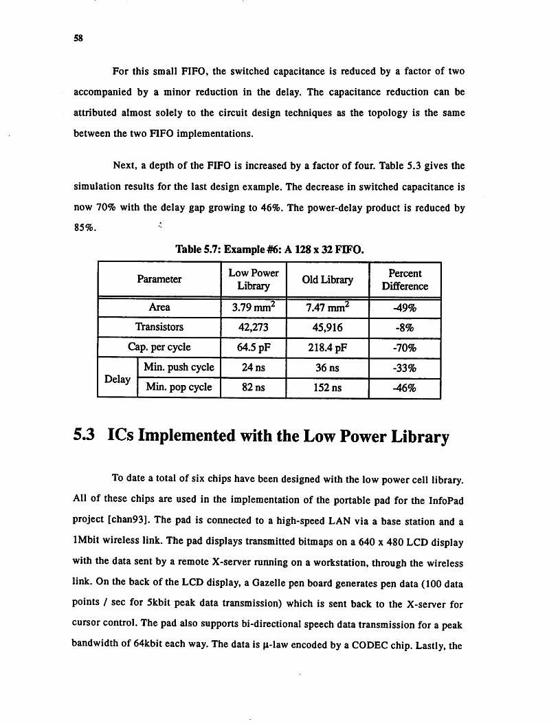
58
For this small FIFO, the switched capacitance is reduced by a factor of two
accompanied by a minor reduction in the delay. The capacitance reduction can be
attributed almost solely to the circuit design techniques as the topology is the same
between the two FIFO implementations.
Next, a depth of the FIFO is increased by a factor of four. Table 5.3 gives the
simulation results for the last design example. The decrease in switched capacitance is
now 70% with the delay gap growing to 46%. The power-delay product is reduced by
85%. ••
Table 5.7: Example #6: A128 x 32 FIFO.
ParameterLow Power
LibraryOld Library
Percent
Difference
Area 3.79 mm2 7.47 mm2 -49%
Transistors 42,273 45,916 -8%
Cap. per cycle 64.5 pF 218.4 pF -70%
DelayMin. push cycle 24 ns 36 ns -33%
Min. pop cycle 82 ns 152 ns -46%
5.3 ICs Implemented with the Low Power Library
To date a total of six chips have been designed with the low powercell library.
All of these chips are used in the implementation of the portable pad for the InfoPad
project [chan93]. The pad is connected to a high-speed LAN via a base station and a
1Mbit wireless link. The pad displays transmitted bitmaps on a 640 x 480 LCD display
with the data sent by a remote X-server running on a workstation, through the wireless
link. On the back of the LCD display, a Gazelle pen board generates pen data (100 data
points / sec for 5kbit peak data transmission) which is sent back to the X-server for
cursor control. Thepad also supports bi-directional speech data transmission for a peak
bandwidth of 64kbit each way. The data is n-law encoded bya CODEC chip. Lastly, the

59
pad's downlink receives a 700kbit compressed video data stream, which is de
compressed and sent to a 240 x 128 color LCD display. The remaining downlink
bandwidth is utilized by the X-server as necessary for screen updates.
All of the chips dissipate below 2mW with some as low as 100u.W. If these
chips were designed without consideration for low-power operation, they would
dissipate power on the order of 250mW to 1W - more than a two-order of magnitude
increase. But, by optimizing power at all levels of the design process as outlined in
Chapter 1, ultra-low power operation is possible to drastically increase the battery life
of the pad. Shifting from 5V operation to 1.5V operation is responsible for the largest
drop in power dissipation. To gain this factor of 10 drop in power, the architecture and
algorithms had to be redesigned to support much longer gate delays. The utilization of
the low power library is responsible for another drop of 3-4. Architectural, algorithmic,
and system design decisions are responsible for the remaining reduction in power
dissipation.
5.3.1 Low Power 64k SRAM Chip [burs94]
A large amount of memory is required by the pad for the video and text/
graphics LCD frame buffers. A total of six chips were used for the text/graphics frame
buffer, while the video frame buffer was integrated on chip with some of the
decompression circuitry and is discussed in a later section. All the SRAMs have 32-bit
wide words. The 64k SRAM chip is broken into eight sub-blocks so that only one block
is active per access. This yields a power reduction by almost a factor of eight. Table 5.8
gives the vital statistics for the SRAM chip. The entire text/graphics frame buffer
dissipates only 3 mW while supporting a 12 ms LCD refresh cycle time.

60
Table 5.8: Statistics for the 64k Low Power SRAM chip.
Parameter Value
Technology 1.2 |xm, double metal process
Size 7.8mm x 6.5mm
Number of Transistors 428,800
Power @ 1.5V, 375kHz cycle time 500 ^iW
Minimum Access Time @ 1.5V 150 ns
5.3.2 Protocol Chip [chan94]
This chip performs several functions. First, the receiver/transmitter modules
multiplex and de-multiplex the data streams from the half-duplex radio to the separate
I/O modules. The pen module is a simple interface between the transmitter module and
the external serial controller that connects to the pen board. The speech module is
another simple interface between the receiver/transmitter module and the external
CODEC. The text/graphics module is slightly more complex as it is responsible for
reading/writing the frame buffer, controlling the LCD display, and interfacing to the
receiver module. FIFOs are used in each of the I/O modules to buffer the data and
asynchronously connect all the modules together. Each module operates at a different
clock rate, so it is not possible to use a single global clock. Table 5.9 gives the vital
statistics for theProtocol chip. Under normal operation it only dissipates 1.9mW.
Table 5.9: Statistics for the Protocol Chip.
Parameter Value
Technology 1.2 ^im, double metal process
Size 9.4mm x 9.1mm
Number of Transistors 136,000
Power @ 1.5V 1.9 mW

61
5.3.3 Video Decompression Chip Set [chan94].
This collection of four chips performs vector quantization decompression of
the serial video data stream coming from the radio. The video controller chip is
responsible for demultiplexing the serial data into luminance, chrominance, and
codebook data. It also maintains global synchronization and generates the NTSC timing
required by the LCD. The luminance decompression chip contains the frame buffer for
the compressed luminance data and the lookup table containing the luminance
codebook data. It performs decompression as the data is read out of the frame buffer.
The chrominance decompression chip performs the same operations on the chrominance
data stream. Lastly, the color space translator chip transforms the incoming digital YIQ
data from the decompression chips to analog RGB data that is sent to the LCD. Table
5.9 gives the vital statistics for the entire chip set. All four chips dissipate less than
2mW, combined, while decompressing data at a rate of 30 frames/sec.
Table 5.10: Statistics for the Video Decompression Chip Set.
Parameter
Value
Controller
ChipLum. Chip Chrom. Chip
Converter
Chip
Technology 1.2 Jim, double metal process
Size (mm x mm) 6.7x6.4 8.5x6.7 8.5x9.0 4.1x4.7
Number of Transistors 31,400 -250,000 -400,000 12,500
Power @ 1.5V 150 pW 115 pW 100 p.W 1.1 mW

Conclusions6
6.1 Summary
A low-power design methodology has successfully been developed and used to
implement the low power cell library in this work. The library is composed of a
standard cell library, a datapath cell (dpp) library, a tiled-cell-array library (TimLager),
and a CMOS 1.2u,m pad library.
Results show that the library provides a factor of two to three energy (average
switched capacitance) reduction over its predecessor library. In some cases, as
demonstrated in Section 5.2, much greater power reduction can be achieved. In addition
to the power reduction, the dpp and TimLager library implementations have delay
reductions of up to 20% and area reductions up to 50%. Lastly, the versatility of the
library has been expanded beyond the original library's scope with the addition of
several new library cells. This generates more compact and efficient layout as some
cells in the new library replace combinations of several sub-cells in the old library.
The library has been integrated into the LagerlV CAD Suite. Also, the
Viewlogic to Oct interface has been completed allowing circuit design via schematic
entry. The entire cell library has been characterized for average switched capacitance,
delay, and area; utilizing these values, the circuit designer can make reasonable
62

63
estimates for chip/module power dissipation, maximum operating speed, and die area
from just high-level architectural descriptions.
6.2 Future Work
The library has been under development for two years and is reaching a mature
state. The culmination of this work will be to release the library through the Mississippi
State University Lager distribution channel. The library has been used in the design of
seven chips, with several more in the final design stage. The heavy usage has helped
detect many bugs found in the library. At present, almost all of the library cells have
been used by one or more chip designs, verifying correct operation.
Currently, ROM and PLA cells are being designed for usage in the TimLager
library. Other cells will most likely be added in the future as the need for them arises.
The process of adding new cells is fairly simple as the library data base is modularized
by cell, and not incorporated as a single flat entity. To add a new cell, all that is
required is the layout, a netlist description of the external terminals, a Viewlogic
symbol, and a VHDL description.
Since the layout adheres to the MOSIS Scalable CMOS Design Rules, the
library can easily migrate to smaller geometry fabrication processes. The only
modification required is to update the delay times and capacitance values in the data
sheets and VHDL models through SPICE simulations of the library cells using an
updated technology file. To utilize other metal layers that may be available on more
advanced processes, however, would require redoing the entire library layout.

Appendix A
Complete Cell Library Listing
This Appendix contains the detailed cell listing of the four different libraries.
Included in the listing are cell names, brief cell descriptions, and I/O terminals.
Below is a list of the subsequent appendix sections:
A.l: Standard Cell Library
A.2: Datapath Library
A.3: TimLager Library
A.4: CMOS 1.2um Pad Library
Furthermore, there is a set of library documentation that exists, above and
beyond what is given in the following four sections. These documentscompletely detail
all cell schematics, cell operation, delay breakdowns, and capacitance breakdowns. On
the zabriskie.eecs.berkeley.edu cluster, the documentation can be found as follows:
Root Directory: ~lager/common/LagerIV/cellib/low_power
Standard Cell Library: RootDir/stdcell2_31p/doc/stdcell2_31p.doc
Datapath Library: RootDir/dpplp/doc/<cellname>.doc
TimLager Library: RootDir/TimLager/blocks/<cellname>/<cellname>.doc
CMOS Pad Library: RootDir/padl_2c/pads.doc
64

The following are examples of the type of further documentation available:
Description.: (Briefly describes functionality of Standard Cell and Pad Libraries)
Stdcell2_3lp Library: CellIIO andFunctionality.
65
Cell Name vo Fanin Cell Description
labflll RSTl,SET2,Q,Q_b 1.3,1.3 Cross-coupled NAND Latch
labf211 RSTl,SET2,Q,Q_b 2.3,2.3 Cross-coupled NOR Latch
Functionality? (Describes more complex functionality of Datapath, TimLager libraries)
Counter: Bit Slice Functionality
Inputs Output
IN RST LD CNT CLK OUT
X X X X 0 OnX X X X 1 On
X 1 X X t 0
0 0 1 X t 0
1 0 1 X t 1
X 0 0 0 t On
X 0 0 1 t Qn+1
Parameters:
N: Number of Bits (#>0)
CLKINV: Set high to invert the clock -> makes register falling-edge triggered.
DOWN: Set high for a Down Counter. CNT and OUT Feedback are inverted.
FB: Set high -> static feedback placed around output inverter, low --> noFB.
Control Signals:
CLK: Counter Clock, (input)
CNT: Count signal (input)
LD: Load signal. Has precedence over CNT (input)
RST: Synchronous reset signal. Has precedence over LD and CNT. (input)
COUT:Carry out from MSB bit slice to detect overflow. Insignificant on theDown Counter(output)

66
Naming: (An example of the description of the Standard Cell Library namingconvention. It is a superset of the 2.2 ITD naming convention [brod88].)
AA A A D
Flip-Flops and Latches -«••
D D
{One ofSevenCategories)
drive capability: IX, 2X, etc.
output type: 0 = normal1 = complementary2 = enabled
internal construction: 1 = NAND/NAND2 = NOR/NOR3 = T-gate4 = TSPC Style Logic
type: f= fixedg = generator
set & rst controls: n = neitherr = reset onlys = set onlyb = both set & reset
latch type: df = D type flip-flopjk = JK type flip-flopla = latchsi = scan latchsd = scan register (D FF w/ TSPC logic)
Schematics,: (An example from the Standard Cell Library. Found in all library documentation)
2)dfhf401,dfnf411
CLK2
DATA1
{cell name(s))
Addition to dfnf411

67
Timing: (An example from the Standard Cell Library. Found in all library docs)
Stdcell2Jlp Library: Estimated (SPICE) Cell Delays
CELL
labflll
labf211
DELAY PATH
RSTl/SET2->
Q/Q_b
RST1 -> Q,SET2 -> Q_b
LOAD
0.5 X
1.0 X
0.5 X
1.0 X
Vdd=1.2V Vdd=1.5V
10.5,17.3 4.4,7.4
14.1,24.6 5.9,10.4
20.5,9.6 8.9,4.2
27.8,11.5 12.0,5.2
NOTE: All delays in nsec. A load of IX is equivalent to 125fF
Vdd=2.1V Vdd=3.0V
1.9, 3.3 1.1, 1.9
2.5,4.6 1.4,2.6
3.9, 1.9 2.3, 1.2
5 .5,2.5 3.1, 1.5
Capacitance- (Characterizations of average effective switched capacitance for librarycells. The following is one of the more complex characterizations.)
TSPCRegister Cell: Estimated(SPICE) Capacitance Breakdown
INSTANCE Total InterconnectCapacitance
(Gate and Diffusion)Input
Capacitance
Bitslice 67.2 fF 14.8 fF (22 %) 52.4 fF (78%) 10.1 fF
CS: tspcr_csl 67.0 fF 3.0 fF (4%) 64.0 fF (96%) 20.1 fF
CS: tspcr_cs2 84.0 fF 3.0 fF (4 %) 81.0 fF (96%) 20.1 fF
CS: tspcr_cs3 117.4 fF 5.0 fF (4 %) 112.4 fF (96%) 20.1 fF
CS: tspcr_cs4 203.5 fF 8.0 fF (4 %) 195.4 fF (96%) 20.1 fF
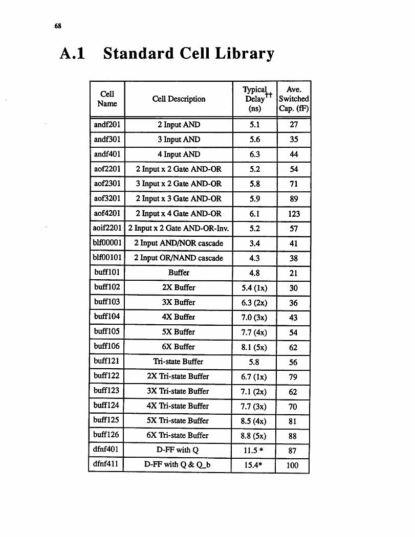
68
A.l Standard Cell Library
Cell
NameCell Description
TypicalDelay*7(ns)
Ave.
Switched
Cap. (fF)
andf201 2 Input AND 5.1 27
andf301 3 Input AND 5.6 35
andf401 4 Input AND 6.3 44
aof2201 2 Input x 2 Gate AND-OR 5.2 54
aof2301 3 Input x 2 Gate AND-OR 5.8 71
aof3201 2 Input x 3 Gate AND-OR 5.9 89
aof4201 2 Input x 4 Gate AND-OR 6.1 123
aoif2201 2 Input x 2 Gate AND-OR-Inv. 5.2 57
blfOOOOl 2 Input AND/NOR cascade 3.4 41
blfOOlOl 2 Input OR/NAND cascade 4.3 38
bufflOl Buffer 4.8 21
buffl02 2X Buffer 5.4 (lx) 30
buffl03 3X Buffer 6.3 (2x) 36
buffl04 4X Buffer 7.0 (3x) 43
buffl05 5X Buffer 7.7 (4x) 54
buffl06 6X Buffer 8.1 (5x) 62
buffl21 Tri-state Buffer 5.8 56
buffl22 2X Tri-state Buffer 6.7 (lx) 79
buffl23 3X Tri-state Buffer 7.1 (2x) 62
buffl24 4X Tri-state Buffer 7.7 (3x) 70
buffi25 5X Tri-state Buffer 8.5 (4x) 81
buffl26 6X Tri-state Buffer 8.8 (5x) 88
dfhf401 D-FF with Q 11.5* 87
dfhf411 D-FFwithQ&Q_b 15.4* 100

CeU
NameCell Description
TypicalDelay™(ns)
Ave.
Switched
Cap. (fF)
dfrf401 D-FFwith Q & async. RST 12.4,7.7** 94
dfrf411 D-FFwith Q, Q_B, & async.RST
15.8,10.9** 106
driflOl lpF Driver 8.1 (0.8pf) 77
drifl02 2pF Driver 7.8 (1.5pF) 149
drifl03 3pF Driver 8.0 (2.5pF) 222
drifl04 4pF Driver 7.8 (3.5pF) 304
drifl05 5pF Driver 13.0 (4.5pF) 400
fafflOl Full adder, two-gate carry delay 16.0,6.8*** 157
fafOll Full adder, one-gate carry delay 18.9,3.9*** 172
fsfOOl Full sub., two-gate carry delay 16.5,6.8*** 157
fsfOll Full sub., one-gate carry delay 20.2,3.9*** 172
haflOOl Half adder 7.5 70
hsfOOl Half subtracter 7.4 71
invflOl Inverter 3.5 10
invfl02 2X Inverter 3.5 17
invfl03 3X Inverter 3.4 24
invfl04 4X Inverter 3.4 34
invfl21 Tri-state Inverter 4.3 43
invf201 Dual Inverter 3.5 21
invf202 2X Dual Inverters 3.5 37
labflll Cross-coupled NAND latch 5.9 38
labf211 Cross-coupled NOR latch 6.7 50
lrbf202 Logic-ref, to both Vdd & GND NA NA
muxf201 2 Input x 1 Select MUX 5.1 67
muxf251 2 Input x 2 Select MUX 5.2 55
rnuxBOl 3 Input x 2 Select MUX 6.4 145
69
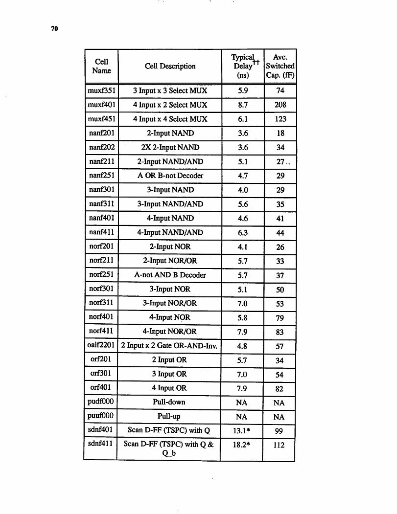
70
Cell
NameCell Description
TypicalDelay77(ns)
Ave.
Switched
Cap. (fF)
muxf351 3 Input x 3 Select MUX 5.9 74
muxf401 4 Input x 2 Select MUX 8.7 208
muxf451 4 Input x 4 Select MUX 6.1 123
nanf201 2-InputNAND 3.6 18
nanf202 2X2-InputNAND 3.6 34
nanf211 2-InputNAND/AND 5.1 21.
nanf251 A OR B-not Decoder 4.7 29
nanf301 3-InputNAND 4.0 29
nanf311 3-InputNAND/AND 5.6 35
nanf401 4-InputNAND 4.6 41
nanf411 4-InputNAND/AND 6.3 44
norf201 2-Liput NOR 4.1 26
norf211 2-Input NOR/OR 5.7 33
norf251 A-not AND B Decoder 5.7 37
norf301 3-Input NOR 5.1 50
norfBll 3-Input NOR/OR 7.0 53
norf401 4-Input NOR 5.8 79
norf411 4-Input NOR/OR 7.9 83
oaif2201 2 Input x 2 Gate OR-AND-Inv. 4.8 57
orf201 2 Input OR 5.7 34
orBOl 3 Input OR 7.0 54
orf401 4 Input OR 7.9 82
pudfOOO Pull-down NA NA
puufOOO Pull-up NA NA
sdnf401 Scan D-FF(TSPC) with Q 13.1* 99
sdnf411 Scan D-FF(TSPC) with Q &Q_b
18.2* 112
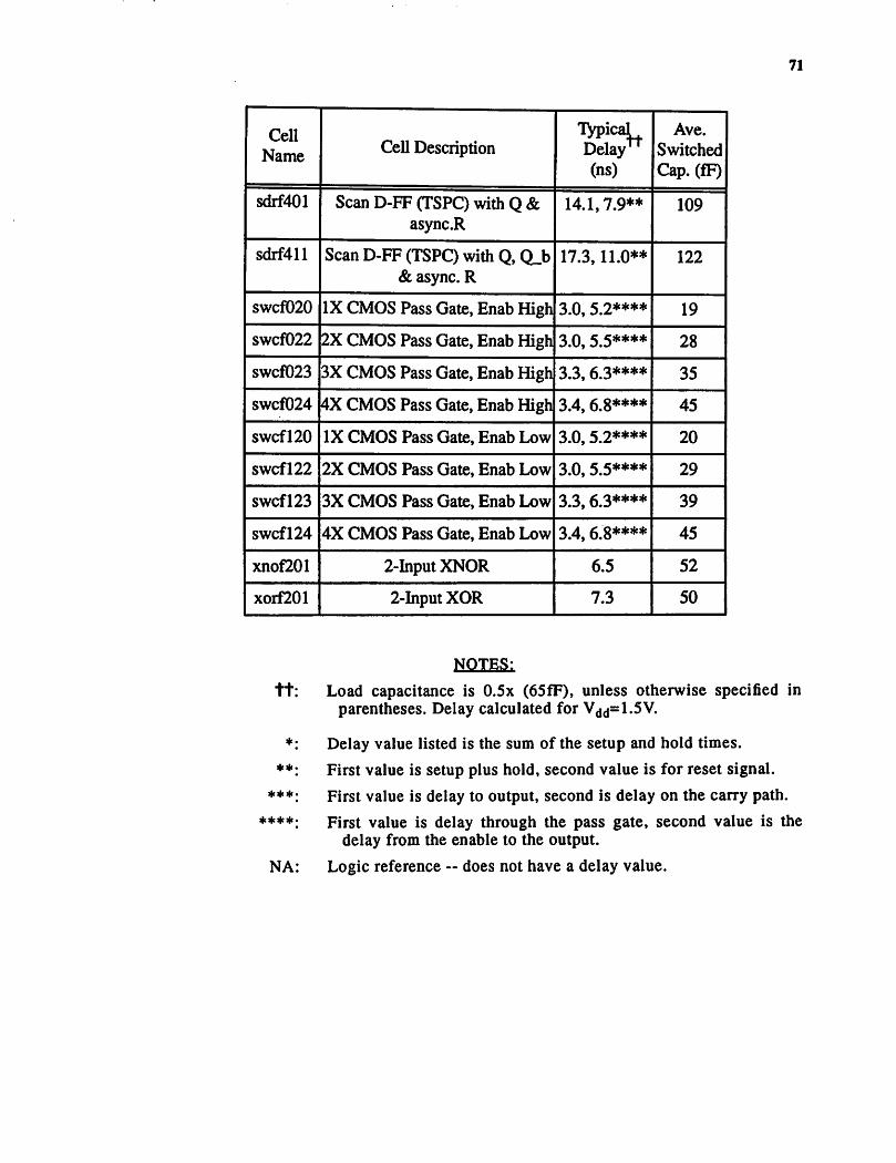
Cell
NameCell Description
TypicalDelay77(ns)
Ave.
Switched
Cap. (fF)
sdrf401 Scan D-FF (TSPC) with Q &asyncR
14.1,7.9** 109
sdrf411 Scan D-FF(TSPC) with Q, QJ>& async. R
17.3,11.0** 122
swcf020 IX CMOS PassGate, Enab High 3.0,5.2**** 19
swcf022 2X CMOS PassGate, Enab High 3.0,5.5**** 28
swcf023 3X CMOS PassGate, Enab High 3.3,6.3**** 35
swcf024 4X CMOS Pass Gate, Enab High 3.4,6.8**** 45
swcfl20 IX CMOS Pass Gate, Enab Low 3.0,5.2**** 20
swcfl22 2X CMOS Pass Gate, Enab Low 3.0,5.5**** 29
swcfl23 3X CMOS Pass Gate, Enab Low 3.3,6.3**** 39
swcfl24 4X CMOS Pass Gate, Enab Low 3.4,6.8**** 45
xnof201 2-InputXNOR 6.5 52
xorf201 2-InputXOR 7.3 50
71
NOTES:
tt: Load capacitance is 0.5x (65fF), unless otherwise specified inparentheses. Delay calculated for Vdd=1.5V.
Delay value listed is the sum of the setup and hold times.
First value is setup plus hold, second value is for reset signal.
First value is delay to output, second is delay on the carry path.
First value is delay through the pass gate, second value is thedelay from the enable to the output.
NA: Logic reference - does not have a delay value.
*
♦*
***

72
A.2 Datapath Library
Cell Name Cell Description OptionsTypicalDelay77
(per bitslice)
Ave. Switched
Cap.(fF per bitslice)
add ripple-carry adder N, CSJTYPE 23.1,1.7** 170
buf buffer N,SIZE 3.2-5.9
/(size)20 -133
/(size)
consh constant shifter N, S, STYPE NA (onlyRC delay)
10-500
/(shift amount)
const constant N,VAL NA NA
counter counter (xl63 functionality) N, CLK-INV,DOWN,FB
12.9,1.8*** 68
csa carry-select adder N, CSJTYPE 20,1.2**** 2£5****
ess carry-select subtracter N, CSJTYPE 20,1.2**** 165****
inv inverter N,SEE 2.4,2.6/(size)
11,24/(size)
logcomp log comparator/greater-then N 3-20***** 200*****
logics random 2,3-input logic cells N,TYPE,NUM_IN
2.4-6.5
f(logic type)10-23
/(logic type)
mux multiplexer N,NUM_IN 4.2,4.7,5.0f(numjn)
62,86,109finumjn)
regfile register file N,R,NC, REG-PLANE
6-25
/(#o/reg.)43/cell
scantspcr scanable tspcr register N, CLKINV,SEDE,FB
10.8* 74
sh variable shifter N,MAXSBY,STYPE. END-
TYPE
9-39
/(shiftamount)
10 -1400
/(shift amount)
sub ripple-carry subtracter N, CSJTYPE 23.1,1.7** 170
tribuf tri-state buffer N,SIZE 5.8,6.7,7.7/(size)
56,57,70/(size)
tspcr tspcr register N, CLKINV, FB 9.1* 67
(see next page for notes and a description of options)

73
DESCRIPTION OF OPTIONS-
N: Number of bits. Cells designed for the range 1 to 32, inclusive.
CSJTYPE: Type of LSB carryin - either constant or selectable.
SIZE: Size of inverter/buffer, with a total of 5 sizes.
S: Shift amount for constant shifter.
STYPE: Shift type - either left or right.
VAL: Integer value for constant cell.
CLKINV: Invert clock —registers become falling-edge triggered.
DOWN: Set counter cell to be a down-counter. Default is an up counter.
FB: Put Feedback on registers. This makes TSPC pseudo-static.
TYPE: What type of logic gate to use: and, or, etc.
NUM_IN: Number of inputs.
R: Number of registers in register file.
NC: Number of non-constant registers in register file.
REGPLANE: Constant register values for register file.
SIDE: What side to SCANIN for scantspcr, can scan up or down register.
MAXSBY: Maximum shift for variable shifter.
ENDTYPE: Set variable shifter to either logical shift, or arithmetic shift.
tt:
*:
**.
NOTES:
Load capacitance is one half the maximum output drive. Forminimum drive, this is 65fF. Delay calculated for Vdd=1.5V.
Delay value listed is the sum of the setup and hold times.
First value is A/B to SUM delay, second value is delay on thecarry path.
First value is IN/OUT to OUT delay, second value is delay on thecarry path of the half adder.
First value is A/B to SUM delay, second value is delay on thecarry path. Delay and capacitance values averaged over a 32-bitcell, since there are several types of bitslices.
Delay varies over levels (1 - 5) in the comparator tree. Capacitance values averaged over a 32-bit cell, since there are severaltypes of bitslices.

74
A.3 TimLager Library
A.3.1 FIFO Cell
DESCRIPTION OF OPTIONS:
N: Number of bits. FIFO optimized for 32 bits, but can operate from8to 48. Values outside this range not verified.
D: Depth of FIFO. Designed for operation from 4 to 256. Valuesoutside this range not verified.
Width DepthPush Cycle
Time
Pop CycleTime
Ave. Switched
Capacitance
32 16 17ns 35ns 25pF
32 32 18ns 46ns 33pF
16 32 17ns 44ns 23pF
32 128 24ns 82ns 65pF
32 256 27ns 127ns 97pF
NOTE: Average switched capacitance consists of a push AND pop event, withexactly half of the data bits changing from their previous state.

75
A.3.2 SRAM Cell
WORDS:
BITS:
BLOCKCOLS:
DESCRIPTION OF OPTIONS-
The total number of addressable words. (The actually number ofwords in the array may be made slightly larger for tilingpurposes, but this will not affect the user.)
The number of bits contained in each word.
Specifies how many columns of sram blocks will be in the entiresram. Must be between 1 and 8, inclusive.
Words/block
Bits 1access TcycleAve. Switched
Capacitance per access
16 3 35ns 48ns 12.4pF
16 16 38ns 52ns 26.7pF
16 32 44ns 59ns 45.3pF
64 3 41ns 54ns 15.6pF
64 16 46ns 60ns 33.3pF
64 32 53ns 68ns 54.2pF
128 3 46ns 59ns 18.7pF
128 16 51ns 66ns 40.0pF
128 32 57ns 74ns 67.1pF
NOTE: Data courtesy of Andy Burstein [burs94].

76
A.4 CMOS 1.2|im Pad Library
Cell Name Cell DescriptionTypicalDelay77(ns)
Ave.
Switched
Cap. (fF)
outl_2c Output pad. Can drive up to 25pF. 16.8 1894
inl_2c Input pad. Can drive up to 1.5pF. 7.5 247
nobufl_2c Unbuffered pad w/ ESD protection. NA 175
iosl_2c Single input tristate buffer. Can drive25pF external, 1.5pF internal
15.3,9.9* 2257,276**
iosfl_2c Same as iosl_2c, but has week feedback to hold ios when input tristated.
15.3,9.9* 2258,276**
iodl_2c Double input tristate buffer. Can drive25pF external, 1.5pFinternal.
15.3,9.9* 2190,268**
outlcl_2c Level-converting (low Vdd ->highVdd) output pad. Candrive 25pF.
14.8 2300
inlcl_2c Level-converting (high Vdd ->lowVdd) input pad. Candrive 1.5pF.
9.8 329
iolcl_2c Double input level-converting tristatebuffer. Can drive 25pF external, 0.75pF
internal
14.8,9.8* 2324,343**
clkl_2c Clock input pad. Can drive5pFload. 6.4 476
vddl_2c Power pad. Connects to Vdd pad ring. NA NA
gndl_2c Power pad. Connects to GND pad ring. NA NA
pwrl_2c Powerpad. Isolated from pad rings. NA NA
space l_2c Filler cells to maintain pad ring continuity along the sides and comers,
respectively.
NA NA
cornerl_2c NA NA
tt:
*:
**•
NOTES:
Load capacitance set to max drivable load. Delay calculated forVdd=1.5V, and VddH=3.3V for level-converting pads.
Delay values listed are in->out delay, and out->in delay.
Capacitance values listed are for in->out path, and out->in path.

References
[ayres90] R. Ayres, eL al,SCMOS DesignRules,University of Southern California,InformationSciences Institute, Rev. 6,1988.
[bako90] H.B. Bakoglu, Circuits,Interconnections, and Packagingfor VLSI, Addison-Wesley,Menlo Park, CA, 1990.
[brod88] R.W. Broderson, et. al., LagerlV Cell Library Documentation, Electronics ResearchLaboratory, University of California, Berkeley, June, 1988.
[brod92] R.W. Brodersen, Anatomyof a SiliconCompile, Kluwer, Boston, 1993.[burs94] A. Burstein, Low Power SRAM Cell Documentation, Electronics Research Labora
tory, University of California, Berkeley, 1994.
[chan92] A. Chandrakasan, S. Sheng, R. Brodersen, "Low-Power CMOS Digital Design",IEEEJournal ofSolid-State Circuits, Vol. 27, No. 4, April 1992.
[chan93] A. Chandrakasan,T. Burd, A. Burstein, S. Narayanaswamy, S. Sheng, R. Brodersen,"System Design of a Multimedia I/O Terminal", VLSI Signal Processing, IV, IEEESpecial Publications, 1993.
[chan94] A. Chandrakasan, Low-power CMOS Design, PhD Thesis, University of California,Berkeley, Aug 1994.
[decl93] M.J. Declercq, M. Schubert, F. Clement, "5V-to-75V CMOS Output Interface Circuits", Proceedings ofthe IEEEInternational Solid-State Circuits Conference, SanFrancisco, Feb. 1993.
[dobb92] D.W. Dobberpuhl,et al.,"A 200-MHz 64-bit Dual-issue CMOS Microprocessor",Digital Technical Journal, Vol. 4, No. 4,1992.
[gray93] P. Gray, R. Meyer, Analysisand Design ofAnalogIntegrated Circuits^ Wiley, NewYork, 1993.
[Iand93] P. Landman, J. Rabaey, "Power Estimation for High Level Synthesis", Proceedings ofEDAC'93, Paris, Feb 1993.
[Iand94] P. Landman, J. Rabaey, "Black-Box Capacitnace Models for Architectural PowerAnalysis", Proceedings of the 1994 InternationalWorkshop on Low-Power Design,Napa Valley, CA, April 1994.
[Iett89] E.R. Lettang, Padroute:A Toolfor Routing the BondingPads ofIntegrated Circuits,Master's Thesis, University of California, Berkeley, 1989.
[Iiu93] D. Liu, C. Svensson, 'Trading Speed for Low Power by Choice of Supply andThreshold Voltages", IEEE Journal ofSolid-State Circuits, Vol. 28, No. 1, Jan. 1993.
77
78
[mull86] R. MuUer,T. Kamins, Device Electronicsfor Integrated Circuits, Wiley, New York,1986.
[salz89] A. Salz, M. Horowitz, "IRSIM: An Incremental MOS Switched-Level Simulator",Proceedings ofthe 26th ACM/IEEE Design Automation Conference, June, 1989.
[sech85] C. Sechen, A. Sangiovanni-Vincentelli, "The TimberWolf Placement and RoutingPackage", IEEEJournal ofSolid State Circuits, Vol. 20, No. 2, April 1985.
[segal90] R.B. Segal, BDSYNUsers' Manual, Industrial Liasion Program, University of California, Berkeley, Ver. 1.1,1990.
[sze81] S. Sze, Physics ofSemiconductor Devices, Wiley, New York, 1981.[veen84] H. Veendrick, "Short-Circuit Dissipation of Static CMOS Circuitryand Its Impact on
the Design ofBuffer Circuits", IEEEJournal ofSolid State Circuits, Vol. 19, No. 4,August 1984.
[yuan89] J. Yuan, C. Svensson, "High-Speed CMOS Circuit Techniques", IEEE Journal ofSolid-State Circuits, Vol. 24, No. 1, Feb. 1989