Embed Size (px)
Citation preview

Copyright © 1985, by the author(s). All rights reserved.
Permission to make digital or hard copies of all or part of this work for personal or
classroom use is granted without fee provided that copies are not made or distributed for profit or commercial advantage and that copies bear this notice and the full citation
on the first page. To copy otherwise, to republish, to post on servers or to redistribute to lists, requires prior specific permission.
HIGH-FREQUENCY CMOS CONTINOUS TIME FILTERS
by
H. Khorramabadi
Memorandum No. UCB/ERL M85/19
27 February 1985
HIGH-FREQUENCY CMOS CONTINUOUS TIME FILTERS
by
H. Khorramabadi
Memorandum No. UCB/ERL M85/19
27 February 1985
ELECTRONICS RESEARCH LABORATORY
College of EngineeringUniversity of California, Berkeley
94720

High-Frequency CMOS Continuous Time Filters
By
Haideh Khorramabadi
B.Sc. (Arya-Mehr University of Technology) 1972M.S. (University of California) 1977
DISSERTATION
Submitted in partial satisfaction of the requirements for the degree of
DOCTOR OF PHILOSOPHY
in
Engineering
in the
GRADUATE DIVISION
OF THE
UNIVERSITY OF CALIFORNIA, BERKELEY
Ph. D.
High-Frequency CMOS Continuous Time Filters
Haideh Khorramabadi
ABSTRACT
EECS
Paul R. GrayChairman of Committee
The extension of fully-integrated continuous time filtering technique to high fre
quencies would allow a higher level of integration in systems such as communication
receivers. In the past, the practical implementation of high-frequency continuous time
filters have been hindered by problems such as the sensitivity of high frequency filters
to the integrator nonidealities and center frequency control. In this dissertation these
problems are investigated.
A simple fully-differential integrator, optimized for phase-error cancellation,
forms the basic element: a complete filter consists of intercoupled integrators. The
center frequency of the filter is locked to an external reference frequency by a modified
phase-locked loop. Instead of the voltage controlled oscillator of the conventional
phase-locked loop, an exact replica of the second order section of the main filter is used.
To prove the viability of this technique, a fully-integrated sixth-order bandpass
filter was designed and fabricated. The prototype dissipates 55 mW and occupies 4 mm~
in a 6 fim CMOS technology.

ACKNOWLEDGEMENTS
I wish to express my deepest appreciation to my research advisor Professor Paul
Gray for his guidance, patience and continuous support throughout the course of my
graduate studies. I feel privileged for the opportunity to work with him.
I would also like to thank the EECS faculty especially Professors R. Brodersen. R.
Meyer and D. Hodges for their teachings and advice. The participation of Professors C.
Sequin and M. Klass in my qualifying exam committee is greatly acknowledged.
I am indebted to many of the graduate students in the integrated circuits group,
both past and present, for their assistance and discussions. The laboratory assistance of
D. McDaniel. D. Rogers. R. Hamilton. D. Chan. K. Chan and C. Atases is sincerely
appreciated.
Finally. I would like to express my deep gratitude to my parents for their con
stant support through the long duration of my studies.
This research was supported in part by the National Science Foundation under
Grant ENG-442427 and also by the Mostek Corporation.

TABLE OF CONTENTS
Chapter 1 - INTRODUCTION 1
Chapter 2 - EXTENSION OF LOW-FREQUENCY FREQUENCY-LOCKED
FILTERING TECHNIQUES TO HIGHER FREQUENCIES 4
Chapter 3 - PRACTICAL IMPLEMENTATION OF CONTINUOUS-TIME
HIGH-FREQUENCY FILTERS 7
3.1 Effect of Integrator Non-Idealities on Filter Behavior 7
3.1.1 The Ideal Integrator 7
3.1.2 The Real Integrator 9
3.1.3 Effect of Finite Integrator Q on Filter Behavior 12
3.2 Integrator Design 14
3.2.1 Quality Factor of the Simple Source-coupled Pair Integrator 17
3.3 Resonator Design Considerations 22
3.3.1 Effect of Parasitic Capacitance on the Resonator Behavior 22
3.3.2 Resonator Quality Factor 24
3.3.3 Terminated Resonator Design 26
3.4 Filter Design „ 31
3.5 Final Integrator Design 39
Chapter 4 - LIMITATIONS OF THE IMPLEMENTATION OF MONOLITHIC
CONTINUOUS-TIME FILTERS 41
4.1 Quality Factor Limitations as a Function of Frequency 41
4.1.1 Optimum Input Transistor Channel Length as a Function of Fre
quency 42
i i
111
4.1.2 Worst Case Integrator Quality Factor ~ 42
4.1.3 Maximum Quality Factor of the Filter as a Function of Frequen
cy 47
4.2 Filter Dynamic Range Considerations 50
4.2.1 Distortion in the Integrator Output Signal 50
4.2.1.1 Intermodulation Distortion ~ 51
4.2.1.2 Center Frequency Shift 53
4.2.1.3 Circuit Techniques to Improve the Integrator Linearity 56
4.2.2 Distortion in the Filter Output Signal 64
4.2.3 Noise Performance of the Integrator 64
4.2.4 Noise Performance of the Filter 65
4.3 Effect of Transistor Mismatches 67
4.4 Design of a 500KHz Filter 68
Chapter 5 - CENTER FREQUENCY CONTROL CIRCUIT 72
5.1 The Modified Phase-Locked Loop Concept 72
5.2 The Phase-Locked Loop in the Locked Condition 74
5.2.1 Effect of the Loop Filter on the PLL Behavior 74
5.2.2 Error Between the Locked Frequency and the Reference Frequen
cy 76
5.3 The Phased-Locked Loop Building Blocks 78
5.3.1 Phase Comparator Design ~ 78
5.3.2 Voltage Controlled Filter 81
5.3.3 DC Amplifier Design 89
5.3.4 Loop Filter 91
5.4 Analysis of the Monolithic Phase-Locked Loop 92
Chapter 6 - EXPERIMENTAL RESULTS 99
Chapter 7 - CONCLUSION Ill
Appendix A - HIGH-FREQUENCY CHARACTERISTICS OF MOS TRANSIS
TORS 114
Appendix B - TOTAL OUTPUT NOISE POWER OF THE BANDPASS FILTER
129

CHAPTER 1
INTRODUCTION
High-precision, high-order monolithic filters in the frequency range of lOOKHz to
10MHz have many applications in communication receivers such as AM & FM IF filter
ing and video processing in T.V. circuits. Additional applications include data com
munications and local area networks.
Monolithic filters have been previously successfully applied to voice band applica
tions both by utilizing the switched-capacitor technique and the continuous-time filter
ing method [l] [2]. However, the extension of both techniques to higher frequencies has
been delayed due to many problems.
One promising approach for the implementation of high-frequency filters is the
switched-capacitor technique. Recently a switched-capacitor bandpass filter at the
center frequency of 260KHz has been designed which has shown excellent performance
[3] . Another switched-capacitor filter with low-pass characteristics was reported at a
roll-off frequency of 2.&MHz [4]. One major drawback to this approach is the require
ment of continuous-time prefilters to band limit the input spectrum to reduce the alias
ing effects. Another problem peculiar to the implementation of high-frequency
switched capacitor filters is that due to settling time limitations in state of the art
operational amplifiers, the extension of this technique to higher frequencies requires the
lowering of the ratio of clock rate to center frequency of the filter which brings about
the necessity of higher selectivity for the anti-aliasing prefilters.
Another alternative is to use continuous-time filtering techniques, which do not
have the aliasing problem of sampled-data systems. However, due to the dependence of
the center frequency of the filter on the absolute values of monolithic components such
1
as capacitors and transistor transconducunces. which are both process and temperature
dependent, some extra circuitry is required to control the center frequency of this type
of filters.
This dissertation describes a high-frequency CMOS continuous-time bandpass
filtering technique which utilizes a modified version of the phase-locked loop scheme
introduced by Tan [l]. to precisely control the center frequency of the filter [5] .
In Chapter 2, Tan's approach is reviewed and the problems involved in the direct
extension of this technique to higher frequencies are discussed.
Solutions to the problems hindering the filter design are proposed in Chapter 3.
where a very simple fully differential integrator is described and a sixth-order
bandpass filter is implemented.
In Chapter 4. the limitations of the designed filter are discussed. This includes
finding an upper bound for the filter quality factor as a function of frequency. Noise
and dynamic range considerations are presented in detail followed by a study of the
effect of transistor mismatches on the filter behavior. In the final section, the results
obtained in the previous sections are used to design a 500 KHz filter.
In Chapter 5, the center frequency control circuit is studied and and the design of
the required building blocks is described.
In Chapter 6. experimental results obtained from a monolithic CMOS prototype is
presented. The prototype includes a sixth order bandpass filter with an on-chip phase-
locked loop.
A summary of this research project is presented in Chapter 7.
In Appendix A. the high-frequency characteristics of MOS transistors which are
required for the design of the integrator are studied.
In Appendix B. the total output noise power of an active ladder type bandpass
filter is derived.

CHAPTER 2
EXTENSION OF LOW-FREQUENCY FREQUENCY-LOCKED
FILTERING TECHNIQUES TO HIGHER FREQUENCIES
The frequency-locked continuous-time filtering technique was first introduced in
1977 [l]. A low-pass voice-band filter was designed by using an integrator as the prin
ciple building block. The roll-off frequency of the filter is determined by the time con
stant of the integrators. This in turn is a function of the absolute values of monolithic
components, in this case capacitors and transistor transconductances. which are both
process and temperature dependent. To achieve an accurate filter roll-off frequency, a
phase-locked loop scheme was utilized to lock the roll-off frequency to an external
reference frequency. Because the frequency characteristics of the filter depend only on
the matching accuracy of monolithic components, using this technique eliminates the
requirement of any external trimming.
Fig. 2.1(a) shows the block diagram of the system. The integrator consists of a
JFET transconductance stage followed by a multi-stage bipolar operational amplifier
and a feedback integrating capacitor, as shown in Fig. 2.1(b). The time constant of the
integrators are controlled through the control voltage. Vc. A voltage-controlled oscilla
tor. VCO. in conjunction with a phase-comparator functions as a phase-locked loop. By
choosing the same type of integrator for both the filter and the VCO. the bandwidth of
the filter tracks the frequency of the oscillator.
The extension of this approach to higher frequencies involves several problems:
1) The main problem is that the behavior of high-frequency filters is highly sensitive
to analog integrator non-idealities, particularly the phase shift at the unity-gain
4

EXTERNALFREQUENCY
O—
SIGNALIN
—L_CZr PHASE I. , , ,lcomparalorj i J - LJ
n
^OUTAGE-CONTROLLED1OSCILLATOR
\*i—>
vIy,r VOLTAGE-CONTROLLED ACTIVE FILTE"r]
L_C
W/kWAC3H I
V-
(a)
vcc
•>I *
cVEE
(b)
SIGNALOUT
—-0
Figure 2.1
(a)- Block diagram of Tan's approach to the design of a low-frequencylow-pass continuous-time filter, (b)- Monolithic JFET input integrator.

frequency.
2) The second problem is the realization of a CMOS VCO with stable and repeatable
center frequency in the MHz range.
3) Because the desired filters are often highly selective (high Q ). the power supply
rejection (PSRR) is a critical problem.
4) Finally the feed-through of the reference signal to the output of the filter can
result in the degradation of the dynamic range.
The solution to the first problem will be discussed in detail in Chapter 3. To
overcome the second problem, an alternative scheme is presented in Chapter 5 which
utilizes a voltage-controlled filter VCF instead of the conventional VCO. The last two
problems are minimized by using fully differential architecture for the circuit design.

CHAPTER 3
PRACTICAL IMPLEMENTATION OF CONTINUOUS-TIME
HIGH-FREQUENCY FILTERS
In the monolithic implementation of continuous-time high-frequency filters, the
most important consideration is the effect of the finite integrator quality factor on the
filter performance. This chapter begins with a study of the effect of the integrator non-
idealities on filter behavior. The results of this study are used to design a simple
source-coupled pair integrator. In the final sections, the considerations for the design of
a resonator and the implementation of a sixth-order bandpass filter are discussed.
3.1. Effect of Integrator Non-Idealities on Filter Behavior
As mentioned earlier, the main building block for ladder type active filters is an
integrator. In this section, the quality factor of the integrator is defined in terms of
integrator non-idealities. The effect of the finite integrator quality factor on the filter
behavior is demonstrated through an example.
3.1.1. The Ideal Integrator
The transfer function of the ideal integrator is given by
H(s) = -^ (3.1)s
It has a pole at the origin and exactly 90 degree phase shift at the unity-gain frequency.
In Fig. 3.1 the amplitude and phase response of an ideal integrator is illustrated.
For the purpose of the design of active filters, one useful measure of the integrator
behavior is its quality factor. Qintg .
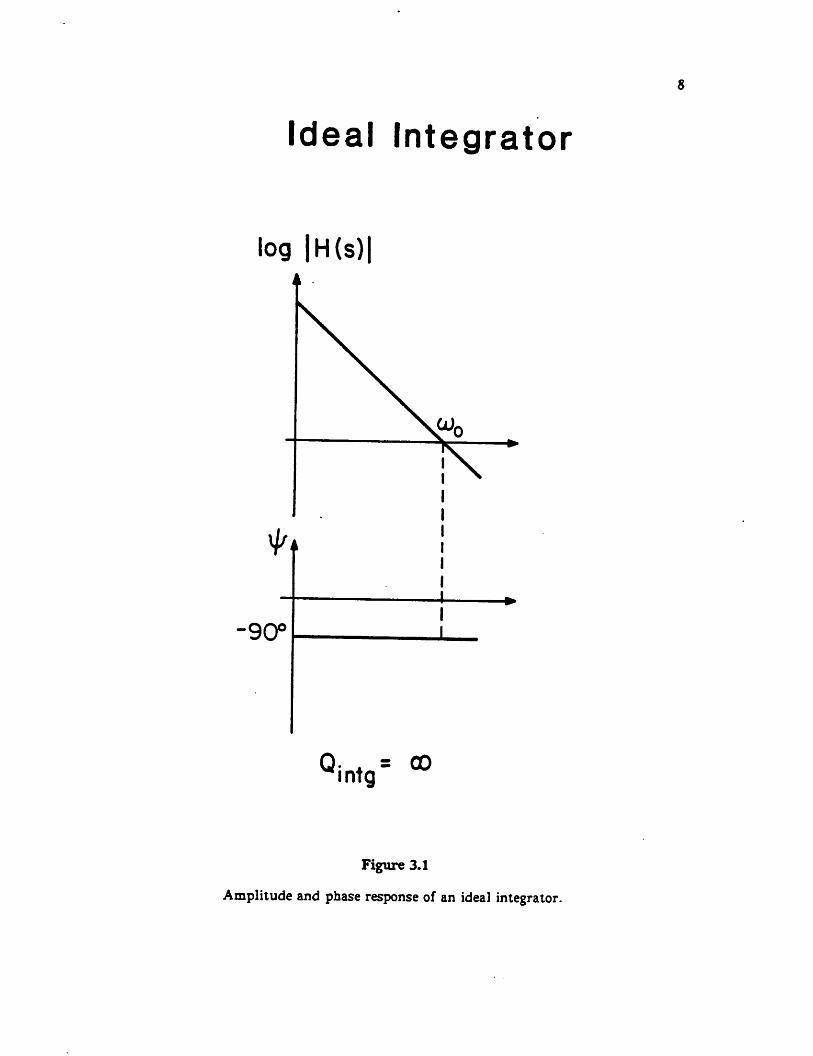
Ideal Integrator
log |H(s)|
*♦
-90°
Qintg* °°
Figure 3.1
Amplitude and phase response of an ideal integrator.

For any component with a transfer function of
*0<a) = xM+jxMthe quality factor is defined as [6]
Q = TUZT
(3.2)
(3.3)
Using the above concept and equation (3.2) . the Q of the ideal integrator is found
to be
r\ ideal _Uinxg ~~ (3.4)
3.1.2. The Real Integrator
For a real integrator, with a finite DC gain of a . the dominant pole is pushed from
the origin to a frequency equal to p i = — . where a>0 is the unity-gain frequency ofa
•the integrator. Also, it may have one or more high-frequency non-dominant poles, P2.
p3 as illustrated in Fig. 3.2. The finite DC gain causes phase lead at the unity-
gain frequency and the non-dominant poles result in excess phase shift.
The transfer function of the real integrator is given by
His) =
1 + s-O)0
1 + J-?2
1 +Pi
(3.5)
To find the quality factor of the real integrator Q^g . the transfer function should be
transformed to the form of the equation (3.2) . The denominator is multiplied and j(o
is substituted for s
H(ju>) =
1+ywx. 1=00 1
—+z~"0 i«2 Pi
—ft)-
i =00 1 •* k =soo 1
^- z — +—L—+MOj^Pj P2k=iPk
+ j(t>'
(3.6)
o>o P2P2
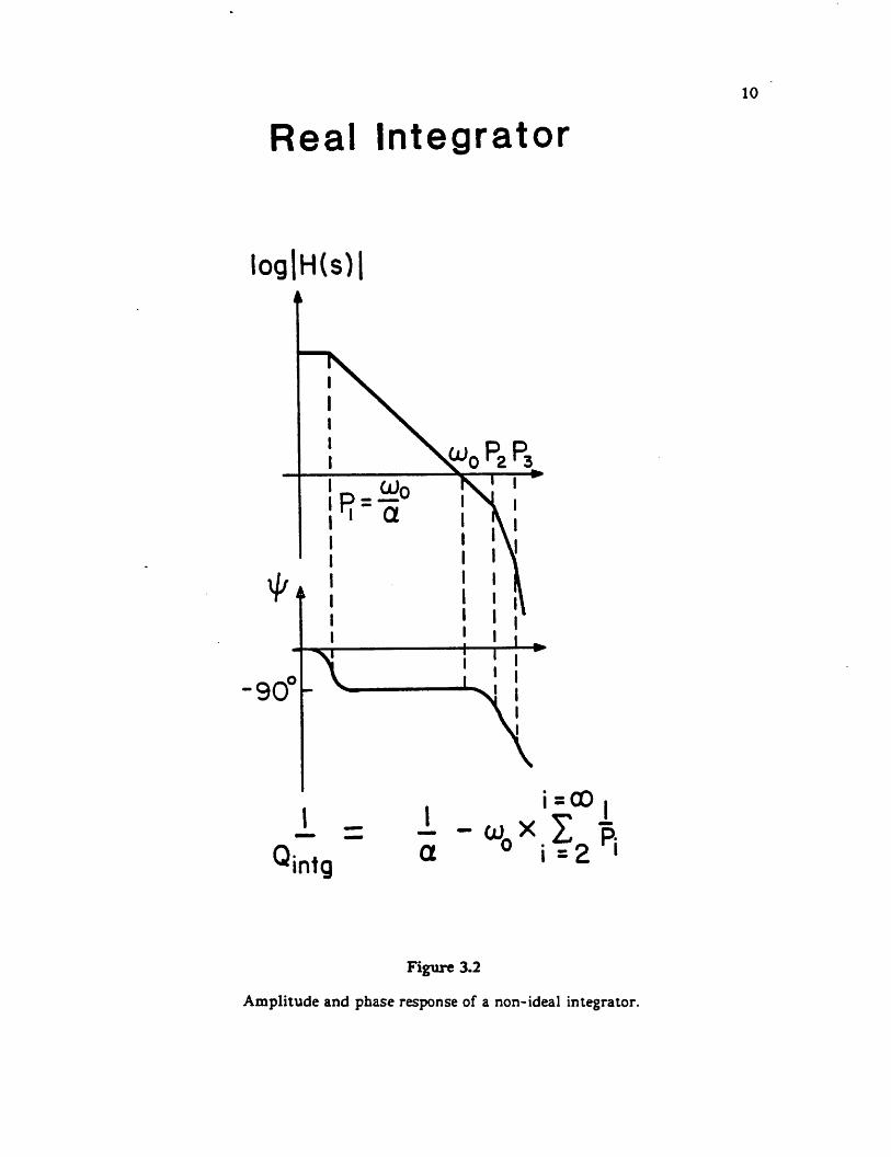
Real Integrator
log|H(s)
intg
i i=COl1 -olX_£_ra i = 2 '
Figure 3.2
Amplitude and phase response of a non-ideal integrator.
10

thus
idi/ug ""*
0>a
6>0
i=oo i
•=2#+ u3 +
1 - cu2*>o ;=2"
*
JU. 1 *=oe 1•i- Z —+ ...P2 k=lPk
+
11
(3.7)
Assuming that all the non-dominant poles />, are at a much higher frequency than the
frequency of interest: that is — «. 1. and that a »1, the quality factor of the real
integrator in the vicinity of the unity-gain frequency, could be simplified as
1Qimg ""*
O)0
CO
1 '^l
a its Pi(3.8)
Note that the quality factor of the real integrator is frequency dependent whereas the
Q of the ideal integrator is equal to infinity for all frequencies.
For w = o»0
Sdinxs """*1
1 lZ? 1— -wol* i=2 Pi
0>0substituting for p i = — from Fig. 3.2 .it can be found that
Qintg ^1
Pi
0>0
'55° 1
i=iPi
(3.9)
(3.10)
The first term is equal to the phase lead at the unity-gain frequency in radians and the
second term corresponds to the excess phase at the same frequency. Note that as o>0 is
increased the excess phase term becomes larger.
12
3.1.3. Effect of Finite Integrator Q on Filter Behavior
The quality factor of the basic element for the implementation of active ladder
filters, the integrator, was found in equation (3.10) . This equation suggests that the
quality factor of the integrator, at a given unity-gain frequency, could be positive,
negative or infinity depending upon the location of the frequency response singularities
with respect to 6>o •
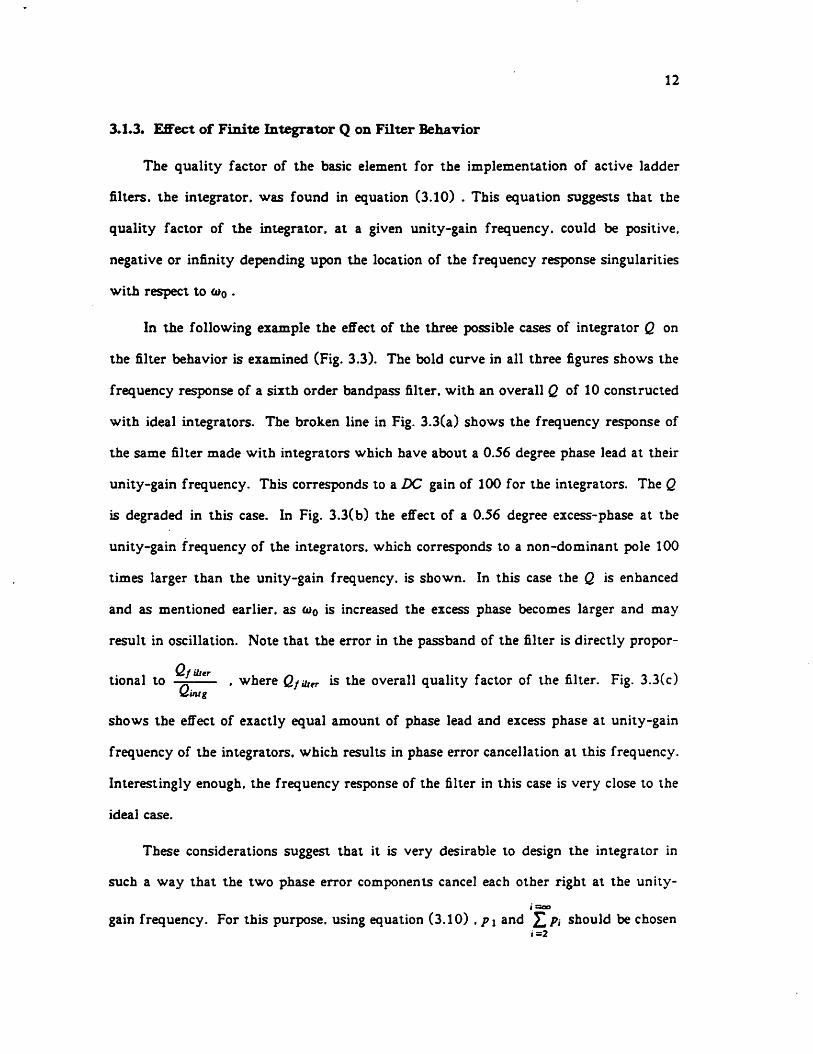
In the following example the effect of the three possible cases of integrator Q on
the filter behavior is examined (Fig. 3.3). The bold curve in all three figures shows the
frequency response of a sixth order bandpass filter, with an overall Q of 10 constructed
with ideal integrators. The broken line in Fig. 3.3(a) shows the frequency response of
the same filter made with integrators which have about a 0.56 degree phase lead at their
unity-gain frequency. This corresponds to a DC gain of 100 for the integrators. The Q
is degraded in this case. In Fig. 3.3(b) the effect of a 0.56 degree excess-phase at the
unity-gain frequency of the integrators, which corresponds to a non-dominant pole 100
times larger than the unity-gain frequency, is shown. In this case the Q is enhanced
and as mentioned earlier, as o>0 is increased the excess phase becomes larger and may
result in oscillation. Note that the error in the passband of the filter is directly propor
tional to * . where Q/uter is the overall quality factor of the filter. Fig. 3.3(c)Qintg
shows the effect of exactly equal amount of phase lead and excess phase at unity-gain
frequency of the integrators, which results in phase error cancellation at this frequency.
Interestingly enough, the frequency response of the filter in this case is very close to the
ideal case.
These considerations suggest that it is very desirable to design the integrator in
such a way that the two phase error components cancel each other right at the unity-
i=oo
gain frequency. For this purpose, using equation (3.10) . p\ and £,Pi should be choseni=2
dB 0.5 u> at cj0.4r lead intg
0.9 1.0
w0
(a)
I.I
dB
4
-6-
-16
-26
0.9
°-5° Excess at <"°intg
/ \_ /
1.0
a*
(b)
dBr (0-5°* ." 0.5°\ff ) at oj(
lead excess Mntg
— terror at "ojntg* °
16
-26«- f
0.9 1.0 I.I
(c)
Figure 33
Effect of integrator non-idealies on the filter behavior.(a)- Effect of 0.5 degree phase lead at (o0 of integrators.
(b)- Effect of 0.5 degree excess phase at cu0 of integrators.(c)- Effect of 0.5 degree phase lead and excess phase at o»0 of integrators.
13
14
so that
n. = a>o'z-^ (3.11)
However, the dependence of the two phase error components on temperature and pro
cess variations limits the accuracy of such phase error cancellation in high-frequency
filtering applications: and thus, in conjunction with the maximum allowable error in
the passband. dictates an upper limit for the maximum Q of the filter. This will be
further explored in section 4.1 .
The passive components, used in the design of conventional LC filters, exhibit a
frequency dependent loss: in other words a finite Q which is always positive. This
results in Q degradation and limits the maximum achievable quality factor of the filter.
Hence, by using the phase-error cancellation technique, the active implementation of
high-frequency filters might have the capability of successfully achieving higher Q's
compared to their passive counterparts.
3.2. Integrator Design
An /?—C integrator is typically constructed of a multi-stage operational amplifier
connected in the feedback configuration shown in Fig. 3.4 . In the previous section, it
was shown that the frequency response of high-frequency filters is very sensitive to
extra phase-shift in the integrator. The high-frequency poles of the multi-stage opera
tional amplifier tend to contribute large amounts of excess phase causing a large error in
the filter response. An important objective, then, is to design an integrator with prefer
ably no non-dominant poles.
To achieve this goal, a one-stage source-coupled differential pair configuration was
chosen to minimize the Q enhancement effects, as shown in Fig. 3.5 . The unity gain
frequency d>0 of this integrator is given by
Figure 3.4
Typical integrator configuration
Vout
W°=RCI
Ol

OUT
control
Figure 3.5
Simple differential pair integrator.
16
«>o -
17
Gm(MU) (3.12)*CauS
where C^g corresponds to the integrating capacitor and Gm(Af is the transconductance
of the input transistors, and for small signals is given by
11/2
%^X(X)<MU)X/rf-U> (3.13)
where /x is the average carrier mobility in the channel. Cox is the gate oxide capacitance
per unit area. W and L are the channel width and length of the input devices and
Jj corresponds to the drain currents. It is evident that o>0 is process dependent and
can be controlled through Cm by varying the drain current of the input transistors
through Vcontrol as described in chapter 5 .
3.2.1. Quality Factor of the Simple Source-coupled Pair Integrator
The quality factor of the integrator Q^g . is found by using equation (3.9). The
first term is derived by finding the DC gain of the integrator. The second term is
estimated by finding an effective non-dominant pole PitttKUvt for l^e integrator.
The DC gain is found to be
a (3.14)
where go(M.,, and go^^ are toe small signal output conductance of the input .transistors
and the load transistors. Assuming that the output resistance of the load transistors is
much larger than the output resistance of the input transistors and by substituting for
= 2Idgm«"» vG5-vrA
and
18
the gain is found to be
where X is the channel-length modulation coefficient. In practice X is estimated from
experimental data and is inversely proportional to the channel length neglecting the
short-channel effects. Here, for simplicity, a new parameter B is introduced
X=1 (3.16)
where 0 is in the order of 0.1
Substituting for X gives
2L
" ' 6(V0S-V,h) (3.17)
Fig. 3.6 shows the small-signal equivalent differential mode half-circuit of the
integrator. The circuit has only two nodes, an input node and an output node. The
simple IGFET model predicts no non-dominant poles for this integrator: in other words,
for a transistor biased in the saturation region, a constant drain current as a function of
frequency is predicted when the gate is driven by a voltage source (Fig. 3.7(a)). How
ever, a more detailed consideration of the distributed nature of the channel resistance
and gate capacitance, as illustrated in Fig. 3.7(b) and Fig. 3.7(c), shows that the fre
quency response of the transconductance falls off at high-frequencies. It can be shown
that this phenomena gives rise to an infinite number of high-frequency poles. In the
previous chapter, it was shown that as long as the non-dominant poles are much higher
in frequency than the unity-gain frequency of the integrator, it is enough to find the
effective non-dominant pole which is at
Mn'~
VOUT
r i<CM,
Figure 3.6
Small signal equivalent differential modehalf-circuit of the integrator.
2C:intg
VO
Vi(Oj)<
20
l*^w) 4.
I
Vi((j) , simple model
m rm
S O-WV '%vtw» • • • \\\U\V-Vvl-VvV<> D
(a)
(b)
i
(c)
2.5f«
Figure 3.7
The high-frequency behavior of an MOS transistor.(a)-Drain current as a function of frequency.
(b)-Cross-section view of an MOS transistor in saturation.(c)-The distributed channel resistance and gate capacitance.

21
te 1Phf/**** "~ 'S°J_ (3.18)
rather than the exact location of each individual pole. In appendix A. it is proven that
in this case
where o>r is the frequency at which the current gain of the input transistor is equal to
one and is given by
&"(AfU> _ 3 m(Vg5-V,a)
±C0XWL * L
Note that the integrator effective non-dominant pole is at a much higher frequency than
for a typical operational amplifier type integrator. The contribution of this phenomena
to the integrator phase shift at the unity gain frequency is
^ Wo 4 <*>oL2<Plag "-T"* = TT" TTf i7—S (3.21)2-5<%Mu) 15 M(VGJ-V,„)(MU)
Substituting from (3.17) and (3.21) in (3.10)
1\diiug """* 0 (Vg5-yrtJ(yu) _ 4 <»oL2 (3.22)
2L 15 m(VG5-V/A)(mu)
Here it is assumed- that the Q of the integrating capacitor is much larger than the other
components quality factor and can be neglected, which is usually the case. The above
equation shows that the excess phase-shift is proportional to L ?M1,) • whereas the
phase lead due to the finite DC gain is proportional to -= . From this the conclu-WW)
sion can be drawn, that for a well-characterized well-controlled process, an optimum
input transistor channel-length can be chosen for first order phase error cancellation at
22
a given frequency which makes the realization of high-<2 filters possible. The optimum
input channel length will be derived in the next section, where the contribution of the
loading integrator to the quality factor of the integrator is also accounted for.
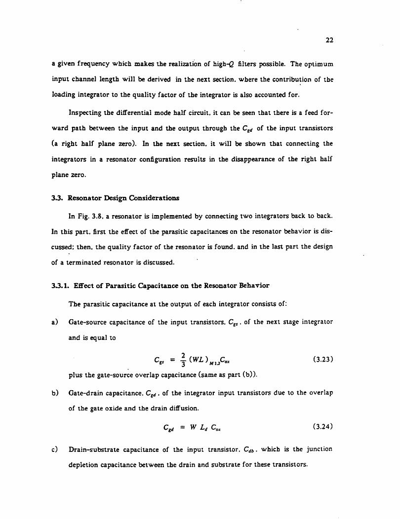
Inspecting the differential mode half circuit, it can be seen that there is a feed for
ward path between the input and the output through the Cgd of the input transistors
(a right half plane zero). In the next section, it will be shown that connecting the
integrators in a resonator configuration results in the disappearance of the right half
plane zero.
33. Resonator Design Considerations
In Fig. 3.8. a resonator is implemented by connecting two integrators back to back.
In this part, first the effect of the parasitic capacitances on the resonator behavior is dis
cussed: then, the quality factor of the resonator is found, and in the last part the design
of a terminated resonator is discussed.
33.1. Effect of Parasitic Capacitance on the Resonator Behavior
The parasitic capacitance at the output of each integrator consists of:
a) Gate-source capacitance of the input transistors. Cgs. of the next stage integrator
and is equal to
Cv = f (WL)„UC„ (3.23)plus the gate-source overlap capacitance (same as part (b)).
b) Gate-drain capacitance. Cgd. of the integrator input transistors due to the overlap
of the gate oxide and the drain diffusion.
Cgd = WLd Cox (3.24)
c) Drain-substrate capacitance of the input transistor. Cat • which is the junction
depletion capacitance between the drain and substrate for these transistors.
Figure 3.8
Circuit configuration of a resonator.
23
24
d) Load transistor capacitance. Cj . which is the capacitance of the load current'load
sources.
e) Parasitic capacitance of the integrating capacitor. C^ . which for a single polynog
process is the junction depletion capacitance between the capacitor bottom plate
diffusion and the substrate.
All of the above capacitances tend to increase the effective value of the integrating capa
citor and therefore increase (Do •
^imgtuat " ^w8 + y2-^/«r (3.25)all
For low frequency applications, where C^g ^Cpar • the parasitic capacitances could be
neglected. At high frequencies, where the size of the integrating capacitors is not
significantly larger than the input transistors, parasitic capacitances should be
accounted for.
3.3.2. Resonator Quality Factor
The resonator quality factor is given be
12 27T- = W=— + 7T— (3.26)Vmtg Qcpar
It can be shown that the overall Q is determined by the larger capacitors and the effect
of the smaller ones is negligible. The largest parasitic capacitance at the output node is
the gate-source capacitance of the input transistors of the next stage. In Appendix A. it
is found that the input impedance of an MOS transistor biased in the saturation region
behaves as a lossy capacitor with a quality factor. Qc s . of
Qc *£*L (3.27)
substituting from (3.22) and (3.27) in (3.26) . the resonator quality factor is found to

25
be
' X ^9(VgrVri)wm _ 4 QqL2 (32&)OT "" L 15 M(vG5-vtA;(AfU)
It is interesting to note that the phase lag term is cut by exactly half due to the loss in
the gate-source capacitances. From the equation above, by equating the two terms, an
optimum channel length for the input transistor is found for which the phase error is
canceled
1/ 3
L0pt "-*15 •»&«-***„„»4 G>0
(3.29)
The above equation suggests that the optimum input transistor channel length is a
function of the center frequency of the filter. As the center frequency is increased.
Lopt, for which the phase error is canceled, tends to decrease. Values for Lopl as a func
tion of the center frequency, are calculated in section 4.1.
One interesting aspect of this resonator circuit configuration is that the right-half
plane zero due to the gate-drain capacitances of the input transistors cancel out. This
can be more clearly understood by inspecting Fig. 3.9 . Let's consider node C. There are
two signal feed-through paths to this node. One is from node A through the gate-drain
capacitance of A/j : the other path runs from node B through the Cgd of A/3 . As the
circuit is fully balanced, the signals at nodes A and B are equal and of opposite signs,
resulting in signal cancellation at node C.
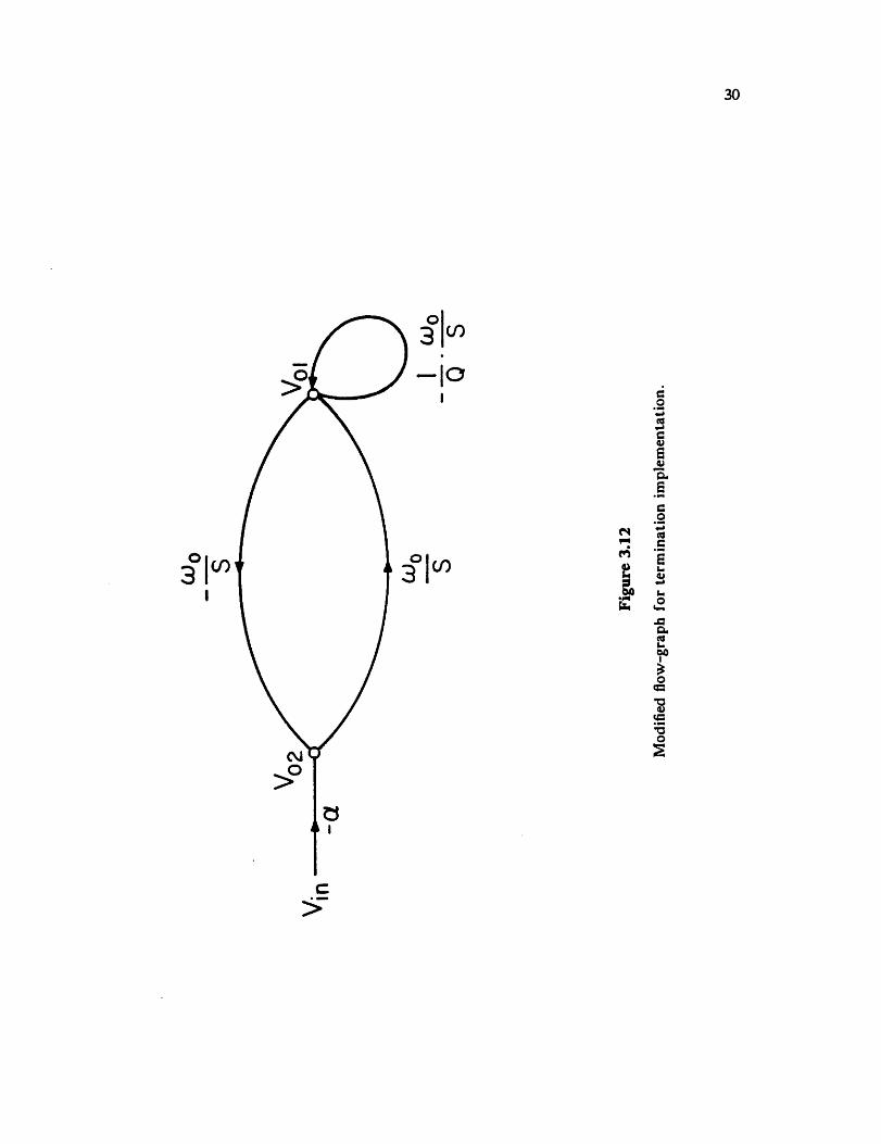
33.3. Terminated Resonator Design
Fig. 3.10 shows the flow-graph of a terminated resonator. Here the termination is
realized by feeding back a fraction equal to 1/ Q of the output of the resonator to its
input.

/
Cgd
Figure 3.9
Feed-through paths to node C of the resonator
26

Vin
-GU
n/S
cu0
/S
Fig
ure
3.1
0
Flo
w-g
raph
of
ate
rmin
ate
dre
sona
tor.
to
^4

28
One approach to this is shown in Fig. 3.11 where the feedback is provided
through a buffer at the output and the capacitor Cq .
Using this configuration the Q is given by
q = iSa. (3.30)
This scheme works well for resonators with low center frequencies . However, at
higher frequencies, the inherent phase-shift between the input and the output of the
buffer distorts the frequency response of the filter.
To overcome this problem the conventional flow-graph is transformed to the one
shown in Fig. 3.12 . This new flow-graph can be realized by adding a resistive load to
the output of one of the integrators. Fig. 3.13 shows a simple implementation of the
resistive load. The equivalent load resistance seen in parallel with the corresponding
integrating capacitor is equal to
*e, - ^ (3.31)m(M3,4)
which results in
Q=̂"(MU) (3.32)m(Af3.4)
wThus, the Q is set by scaling the -=- ratios of M12 and M3A as well as the current
sources. This will be discussed further in section 3.5.
3.4. Filter Design
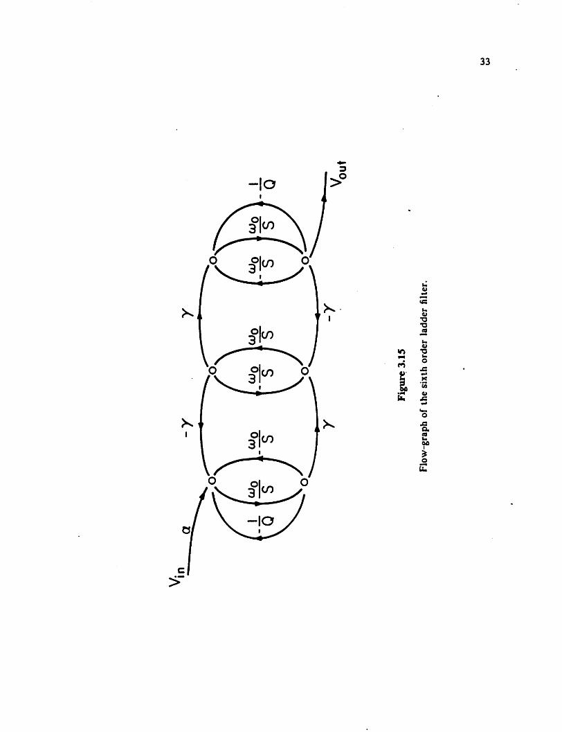
The classical doubly-terminated LC ladder structure was used in the experimen
tal chip described in chapter 6 due to its low sensitivity to component variations (Fig.
3.14)[7],[8]. The flow-graph for such a filter is shown in Fig. 3.15 [9] which is con
structed of three resonators interconnected through unilateral coupling paths. All

If . !]r-4
Figure 3.11
Direct termination implementation.
29
Vin
-a
Fig
ure
3.1
2
Mod
ifie
dfl
ow-g
raph
for
term
ina
tio
nim
ple
men
tati
on
.
8
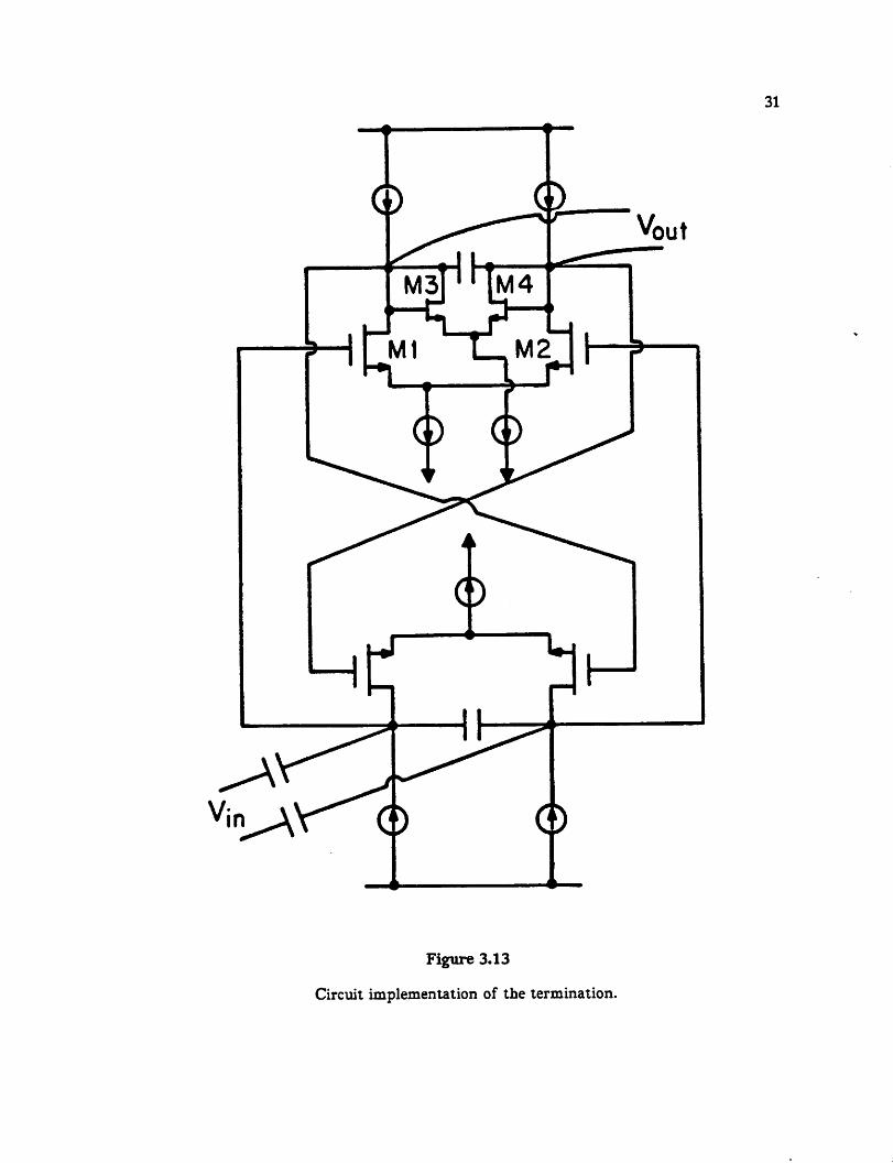
Figure 3.13
Circuit implementation of the termination.
31

RiV|N —VW
Figure 3.14
Sixth order LC ladder filter.
32
OUT
Fig
ure
3.15
Flo
w-g
raph
of
the
sixt
hor
der
ladd
erfi
lter
.
ou
t

34
integrators are chosen to have the same time constant for optimum sensitivity [3].
Using the resonator designed in the previous section, the implementation of the filter
brings about the requirement of buffers at the resonator outputs for the unilateral cou
pling paths. This results in an increased die area and increased power consumption.
Moreover, for filters with high center frequencies, the extra phase-shift caused by the
buffer may result in a significant distortion in the filter frequency response . This
problem can be alleviated by converting the flow-graph to the configuration shown in
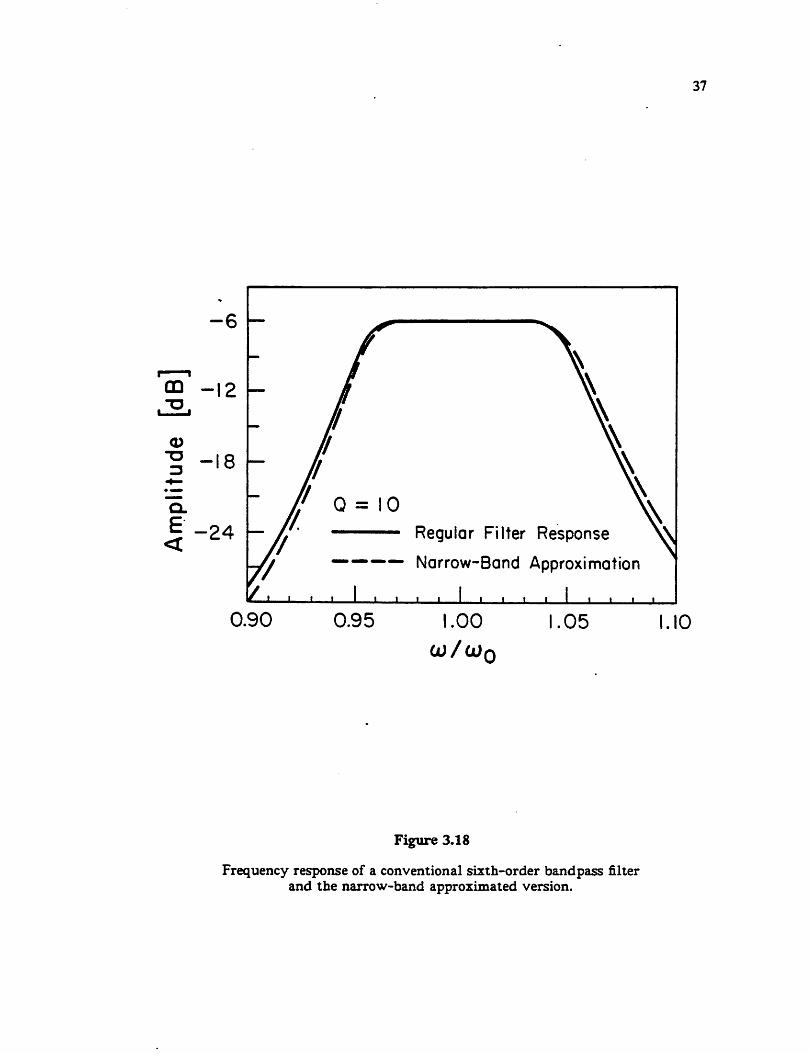
Fig. 3.16. Note that for narrow-band filters, the following assumption is true within
the passband of the filter
!?t = -1 (3.33)s
Using this approximation the coupling paths are transformed to bilateral paths with
equal values as shown in Fig. 3.17. This approximation is called the narrow-band
approximation which exhibits a reasonable passband shape for a Q greater than about 4
[10]. Fig. 3.18 shows the frequency response of a bandpass filter using the conven
tional flow-graph and the frequency response for the narrow-band approximated filler.
By inspecting the frequency response, it can be seen that the narrow-band approxima
tion causes the filter frequency response to be slightly unsymmetrical .
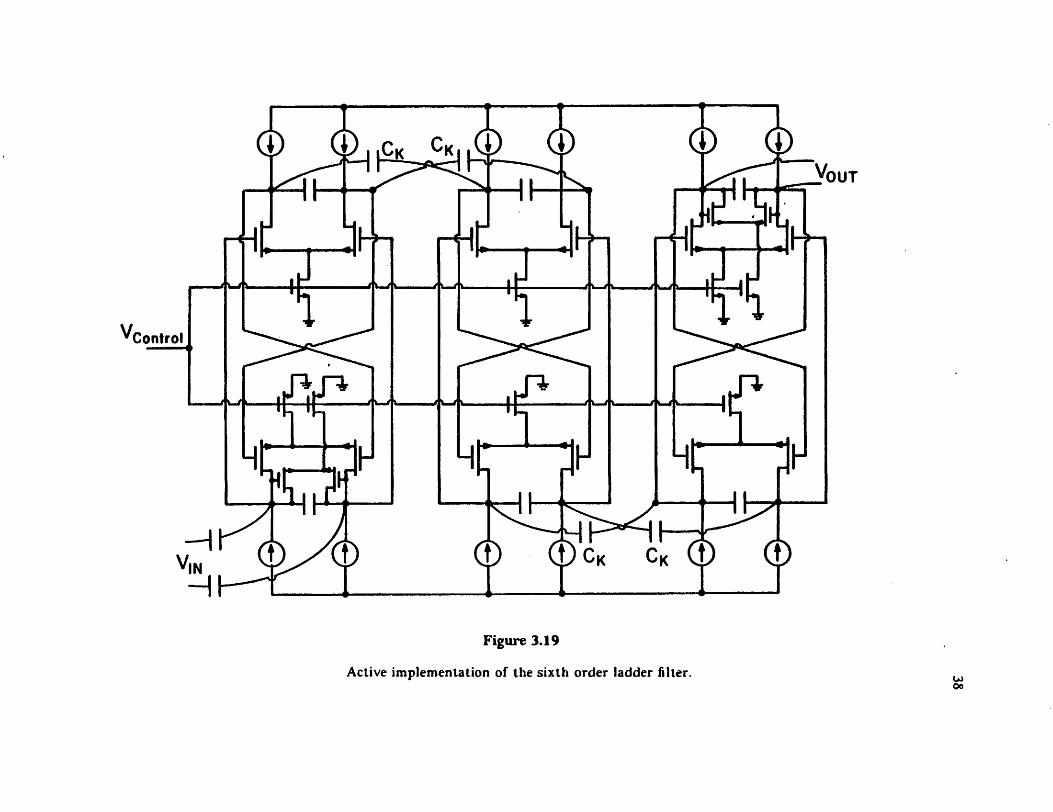
Fig. 3.19 shows the active implementation of a narrow-band approximated
sixth-order bandpass filter using the designed integrator. Note that using the above
approximation, the active realization is simply done by using three resonators coupled
through capacitors (Ck). The coupling coefficient is given by
y=^L (3.34)
The center frequency of the filter is controlled by Vcontrol by varying the transconduc
tance of all input transistors which makes the matching of these transistors critical as
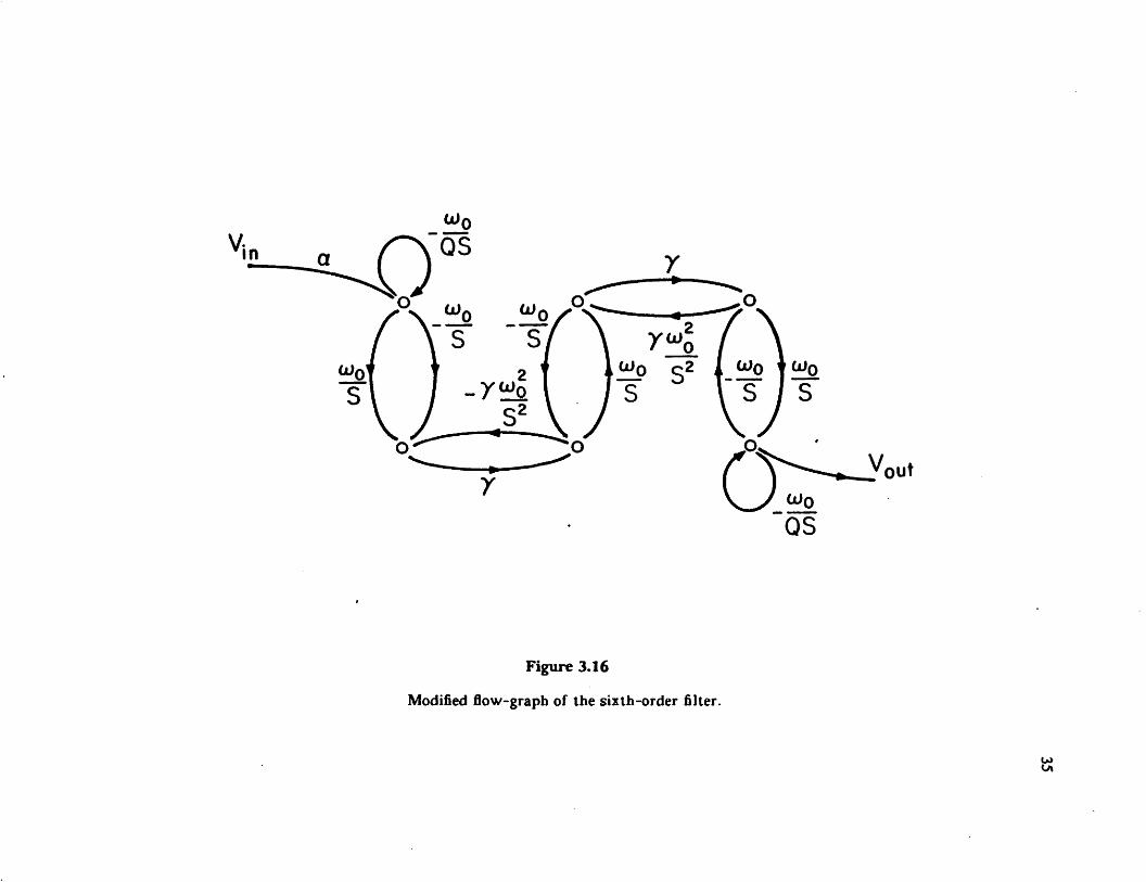
Figure 3.16
Modified flow-graph of the sixth-order filter.

Figure 3.17
Modified flow-graph of the sixth-order filter.
os
-6
CD -12T3t
<D
3-18
• ^H»
"o.£• -?4
<
0 = 10
Regular Filter Response
———— Narrow-Band Approximation
j ' « « i * ' • .1—1 L__L J ' ' '
0.90 0.95 1.00
(jJ/(jJq
Figure 3.18
.05
Frequency response of a conventional sixth-order bandpass filterand the narrow-band approximated version.
37
.10
38
u
T34>uO
4>J=
.2?oocEe><
39
discussed in section 4.3.
The fully differential architecture immunizes the filter response to the power sup
ply variations and parasitic couplings and the reference signal feed-through to the out
put of the filter.
3.5. Final Integrator Design
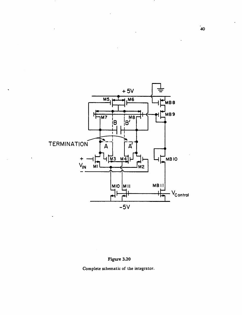
The complete schematic of the integrator is shown in Fig. 3.20. The common
mode output voltage is stabilized by A/5^/6 which operate in the triode region. M3M4
are the termination devices and are connected in the (A —A') configuration for ter
minated integrators: {B—B') connection is made for unterminated integrators for
matching purposes.
The quality factor of a terminated integrator Q-%g was found in section 3.3.
Q
where
term _ mWU>
m(M3.4)
d(M\J) _
d(M3A)
V£ ' (Mil) diM\J)r^
V£ MM 3.4) dlM3.4)
L (A/10)
L (Mil)
(3.35)
(3.36)
By chosing equal channel lengths for M1>2 . A/3.4 and Mi0 . Mn . the Q can be imple
mented by scaling the channel widths of these transistors. To achieve high accuracy for
the Q implementation, the termination transistor is chosen as a unit transistor and the
input transistors are constructed of an array of Q unit transistors connected in parallel.
TERMINATION
+ |̂7h[m3 m^iJJ^ LjrMBioV,N Mil '. j '' Im2
/\ t\
MIO Mil MB
fi-vs3^-5V
Figure 3.20
Complete schematic of the integrator.
Control
40
CHAPTER 4
LIMITATIONS OF THE IMPLEMENTATION OF MONOLITHIC
CONTINUOUS-TIME FILTERS
In chapter 3, a simple integrator was designed and used to construct a sixth-order
continuous-time bandpass filter. In this chapter, the fundamental limitations of such
an approach are investigated.
In the first section, the maximum achievable quality factor of the filter as a func
tion of process parameter variations and the center frequency is discussed in detail.
In the second section, the dynamic range of the filter is determined by finding an
upper and lower limit for an acceptable output signal.
The third section deals with the effect of transistor mismatches on the behavior of
the filter.
Finally, the design of a bandpass filter at the center frequency of 500 KHz is dis
cussed.
4.1. Quality Factor Limitations as a Function of Frequency
In this section the limitations of the quality factor of the filter, imposed by the
process and temperature variations, are studied in detail.
The error in the filter passband is directly proportional to the ratio of *U,er ; in
other words, the maximum achievable filter quality factor. Qfoxer* is dictated by the
maximum allowable passband error and the minimum integrator quality factor Q^g •
In chapter 3. the phase error cancellation technique was proposed to be utilized in
the integrator design. For this purpose, an optimum input transistor channel length
41
42
was derived. Ideally, by using this technique, there should be no restrictions on the
filter quality factor. However, process and temperature variations limit the accuracy of
such phase error cancellation which results in a finite integrator quality factor and
thus, dictates an upper limit for the maximum Q of the filter.
In this section the optimum input transistor channel length is first found as a
function of frequency followed by the derivation of the worst case integrator quality
factor: and then, the maximum quality factor of the filter is derived for different fre
quencies.
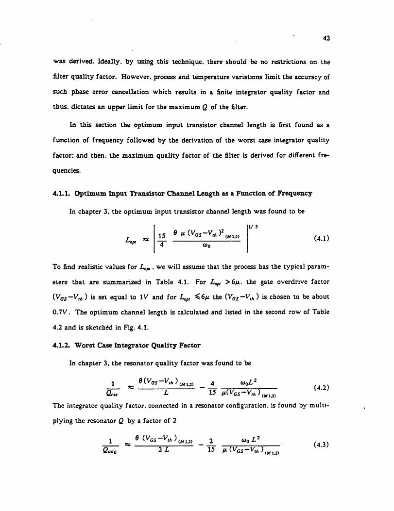
4.1.1. Optimum Input Transistor Channel Length as a Function of Frequency
In chapter 3. the optimum input transistor channel length was found to be
'-'opt *"15 eM(vG5-v,A)2~4~ a>^~
(AM .2) (4.1)
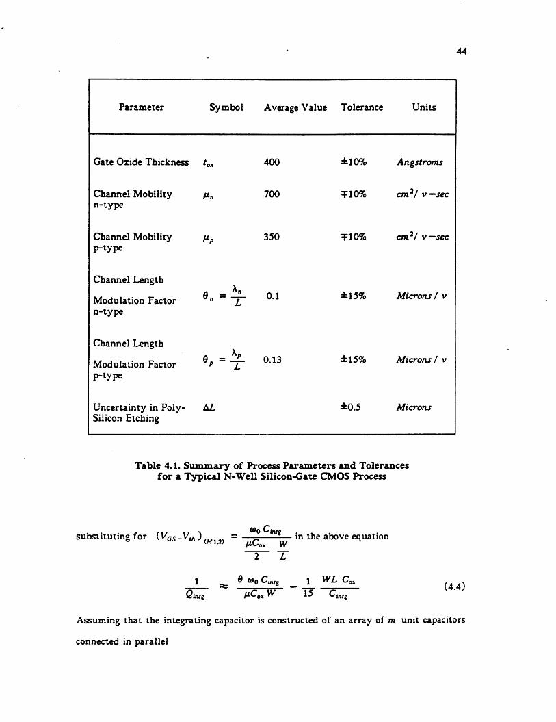
To find realistic values for Lopt. we will assume that the process has the typical param
eters that are summarized in Table 4.1. For Lopl >6/x. the gate overdrive factor
(VG5 —Vth ) is set equal to IV and for Lopt ^6fi the (VG5-V|A) is chosen to be about
0.7V. The optimum channel length is calculated and listed in the second row of Table
4.2 and is sketched in Fig. 4.1.
4.1.2. Worst Case Integrator Quality Factor
In chapter 3. the resonator quality factor was found to be
1 „ g(^G5-^)(MU) __ 4 0>qL2Qres L 15 MVGS-V,A)(MU)
The integrator quality factor, connected in a resonator configuration, is found by multi
plying the resonator Q by a factor of 2
1 ^ 3 (VGS~vth\MU) _ 2_ <»oL2Quug 21 15 /i(VG5-V,A)(Mij)
43
lOOKHz IMHz 10MHz 100MHz
Figure 4.1
Optimum input transistor channel length as a function of frequency.
44
Parameter Symbol Average Value Tolerance Units
Gate Oxide Thickness tox 400 ±10% Angstroms
Channel Mobilityn-type
Mn 700 T10% cm2/ v—sec
Channel Mobilityp-type
Pp 350 T10% cm2/ v—sec
Channel Length
6n ~ —Modulation Factor
n-type
0.1 ±15% Microns / v
Channel Length
A - ^fBP- —Modulation Factor
p-type
0.13 ±15% Microns/ v
Uncertainty in Poly-Silicon Etching
AL ±0.5 Microns
Table 4.1. Summary of Process Parameters and Tolerancesfor a Typical N-Well Silicon-Gate CMOS Process
substituting for (VGS_V|A ) _. ^0 Cinxg(*u) = fiC0X w
2 L
1 ^ 9 VoCintg _Qifug ~~ nC0X w a cmtg
in the above equation
1 WL C0(4.4)
Assuming that the integrating capacitor is constructed of an array of m unit capacitors
connected in parallel
45
Cjntg = m ™ca/> -Leap ^ox^ (4.5)
where W^ and L^ are the width and length of the unit capacitor and are usually
chosen to have equal values and Cox is the capacitor oxide capacitance per unit area.
Substituting for C^g in (4.4)
1 ^ 0 6)0 m W^ L^ ^ox^ \ WL Coxiintg w 15 m Wcap Leap CQXcap (4.6)
For the ideal case, both terms in the above equation are equal thus it is assumed that
each term is equal to jr—. Now the quality factor can be estimated in terms of Q* andSia
the process parameter tolerances by
1 -
Jlfttg Qa
Ad *L +2AWcapw,cap
+2^L'cap
-2AW
W
ACflAO,+ 2-
'cap-2-
'cap
AL
L
(4.7)
The fact that the terms corresponding to the capacitor oxide capacitance and the gate
oxide capacitance are of opposite signs suggests that it is desirable to have a process for
which the gate oxide and the capacitor oxide are grown simultaneously. In this case,
independent of their absolute values, the oxide thickness of the transistor gates and the
capacitors tracks and thus.ACfl
'cap tc*
Cox„. Coxcop
and the two correlated oxide capacitance
errors would cancel each other. The term corresponding to the channel width of the
input transistors could be neglected as usually W »AW. Thus Qinig is simplified and
"~ Qaiuug
Ad *L +2^ +2.^"'w,cap "cap L
(4.8)
To find a worst case value for Q^g . Qa should be estimated from equation (4.3)
2L
a d(vG5-vfJ(AfU)
substituting for Lopt from (4.1)
a =30 ft
e2(vG5-vrA)(MU)a,0
1/ 3
Substituting for (2a • G»«g is found to be
30/t1/ 3
0 . =s i•'Ofc-V* )„,„,«. |
Vitntg
+ * -/* "cap -^cap
AZ,
z.
46
(4.9)
(4.10)
(4.11)
Both the numerator and the denominator, in the above equation, are frequency depen
dent. The numerator. Qa . is proportional to —jj-y. In the denominator. Lopt, W^ and
Leap are functions of frequency and decrease as frequency is increased. Thus the worst
case integrator Q decreases as the frequency is increased.
To find a general idea for the value of (2«ug . for simplicity it is assumed that
♦▼cap "~ •'"cap "*" ^•t-'opt
Using the process parameters and the corresponding tolerances from Table 4.1
-ln ^ 32212*W " / 1/3
7 o0.25+ 2*0-5"
'opr
(4.12)
(4.13)
Using the above equation, the calculated values for Quag for different frequencies is
listed in the third row of Table 4.2.
In the next part, this results are used to find an upper limit for the quality factor
of the filter.

/o Lopt M Qintg Qfilter
100 KHz 34.7 2489 50
200 KHz 27.5 1923.5 38.5
500 KHz 20.3 1356.2 27.1
1MHz 16.1 1032 20.6
2 MHz 12.8 779.2 15.6
5 MHz 9.4 528.6 10.6
10 MHz 7.5 390 7.8
20 MHz 4.7 289 5.8
50 MHz 3.9 194.5 3.9
100 MHz 2.7 126 2.5
Table 4.2. Optimum Channel Length - Minimum Integrator Q -Maximum Filter Q as a Function of Frequency
47
4.1.3. Maximum Quality Factor of the Filter as a Function of Frequency
As mentioned earlier, the maximum achievable quality factor of the filter depends
on the minimum integrator Q and the maximum allowable error in the passband of the
filter.

48
For a resistively terminated LC filter, the fractional change in the magnitude
within the passband could be expressed as [ll]
AT(o>) ^ _1_T{a>) ~~ 2 -L + -L
Ql QcQ>tM (4.14)
where Qi and Qc are the quality factors of the filter inductor and capacitors: r(o>) is
the filter group delay, and o> is the frequency of interest. Similarly for a filter con
structed with integrators
The group delay riot) of a sixth order bandpass filter is at its maximum at the lower
and upper edges of the passband. Using the filter simulation program FILSYN [12]. it
can be shown that for a sixth order bandpass filter designed to have about 0.1 dB rip
ple in the passband
#2l =7.16 (4.16)\lj titer
substituting in (4.15)
*™ * ^HHL x7.16 (4.17)
To find an estimate for the maximum achievable Q/uter> as an example it is
assumed that the maximum allowable passband error is about 1.2 dB. Substituting in
the above equation it is found that
QfUttr * -!_ (4.18)Qintg 48.3
Thus, the integrator Q must be at least about 50 times larger than the filter quality
factor. From the above results and the minimum value found for QM,S (third row of
Table 4.2). the maximum QidltT is calculated and is tabulated in the fourth row of
Table 4.2. The maximum filter Q as a function of frequency is sketched in Fig. 4.2.
The maximum quality factor for a 100 KHz filter is about 50 and the upper limit
of the quality factor of a 100 MHz filter is about 2.5.

100 KHz IMHz 10MHz
Figure 4.2
Maximum filter Q as a function of frequency.
49
lOOMHz
50
4.2. Filter Dynamic Range Considerations
The dynamic range of the filter is defined as the ratio of the total RMS output vol
tage at a given distortion level to the total RMS noise voltage within the passband of
the filter.
For bandpass filters, the maximum signal level is usually defined at a 1% third-
order intermodulation distortion as this is the only distortion component which in most
cases may fall within the passband of the filter, the other distortion components are
filtered out.
The noise at the output of the filter is determined by the sum of the noise contri
bution from each of the integrators.
In the following section, the output signal distortion of the integrator and it's
effect on the filter distortion is discussed first. Some techniques are presented to
improve the dynamic range of the filter. In the next part the noise performance of the
integrator is discussed and the total output noise of second and sixth order bandpass
filters are found.
4.2.1. Distortion in the Integrator Output Signal
The nonlinear behavior of the integrator gives rise to two problems:
1) As the signal level is increased the transfer function becomes more nonlinear
and in the presence of unwanted signals this may result in spurious signals being gen
erated within the pass-band of the filter.
2) The fact that the input transistor transconductance decreases as the signal level
is increased, results in the lowering of the unity-gain frequency of the integrator
(center frequency down shift of the filter). This is especially critical for high-Q filters.
To evaluate the distortion in the output signal of the integrator, it is assumed that
the nonlinearity due to the load transistors is negligible compared to the input

51 N
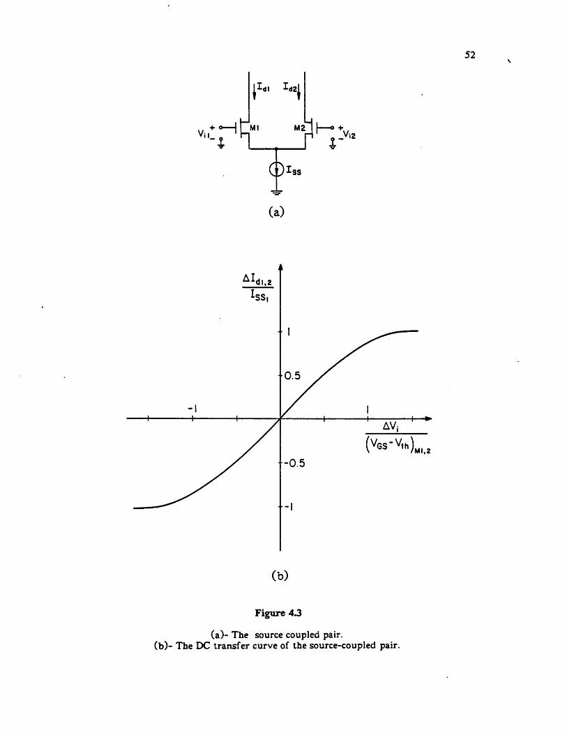
transistors. Fig. 4.3(b) shows the DC transfer characteristics of the integrator input
source-coupled pair of Fig. 4.3(a). The differential output current is found to be
12 m
A/rf = U(^G5-Ha )MU -I
AVj(4.19)
Note that AId reaches its limit. /„ . when Av, ^ v/2(VG5—Vtn ).
Using the series expansion of (1—x2)*. the differential output current could be
transformed to
13
Afc = /,Av,-
(VG5-VrA )Mia
1
128
Av,
(Vcj-V,, )wu
Av,-
(^Gi-VfA )*fU
1024
Av,
(VG5_Vf, )mu
(4.20)
For small input signals. Av, «(VCS—Vlh ). the first term is much larger than the higher
order terms and the output current is a linear function of the input voltage. For input
signals comparable to (VGJ—Vth ). the higher order terms become more significant which
results in nonlinear behavior in the output current.
4.2.1.1. Intermodulation Distortion
As mentioned earlier, for bandpass filters the third order intermodulation. IMS.
component is the only distortion component which may fall within the passband of the
filter. To calculate IM3. the coefficients in the following equation must be found [13]
£Jd = ajv; + a2v2 + a^3 + a4v;4 + a5Vj5 + a6v;6 + (4.21)
from equation (4.20)
l*dl J-dzl
-*rt_J>C)iss
(a)
AIdi,2
^Si
(V«-V-L,
(b)
Figure 43
(a)- The source coupled pair,(b)- The DC transfer curve of the source-coupled pair.
52
a3 = -
a* = —
(VG5 - Vlh )
" &(VGS - VtA )*
128 (VGS - VrA )>
a2 = 0
a4 = 0
fl6 = 0
53
(4.22)
the third order intermodulation component^A/3, is generated by the odd coefficients
and can be shown to be equal to
/A/3 - i»fi V +£^ V +4 O] 5 <Z]
using the values found for a 1 and a 3 and a 5
12
IM 3 as - X3?
Avj
(VG5-Vr, )MU25
1024
Avj
for small values of IM 3. the first term is dominant and
2vimax^4(VG5-Vr/,) IMl
(4.23)
•(4.24)
(4.25)
As expected, the maximum voltage is increased as the gate overdrive voltage (VG5—Vth )
is increased.
For example for IM 3 = 1% and (VGS-V,A ) = 1 V
vjmax= 327 mV or viJtMS = 231 mV (4.26)
The maximum voltage is quite low and can be increased by increasing (VG5—Vth ). The
other factors that limit the choice of this parameter will be discussed later.
4.2.1.2. Center Frequency Shift
The center frequency shift of the filter for large input signals is a particularly
critical problem for the design of high Q filters.
The unity-gain frequency of the integrator is given by
54
o>0 =2C
(4.27)intg
Let's assume Gm is the large signal transconductance of the integrator and gm is the
small signal transconductance
dtJdCm =
t/Av,
differentiating equation (4.20)
Gm =Iss
1 -3
8
AV; 2_ 5 Av .
4
W6S-Vth) (VG5_Vr/l)MU
7
128 | (VG5_VAv,
th )mW6
1024 (VG5-Vr, )MU
bm (vG,-v,J " *• • ""»
or
AG,
-iAv,
(VG5-V|A )MlJ
2
Av,
(Vg.s-V^^u
12
128
7
1024
128
7
1024
Avf
(VG(5_VrA )*fu
Avt-
(VG5_V,A )mu
Av,4
(Vgs_V,a)mu
Avt-
(VG5-VrA )afij
16
For small values ofAG,
gm-. the first term is dominant and
vim« ^ 2(VG5-VtA)
Comparing the above result to (4.25). it is evident that the maximum input voltage is
2 AGr
3 gr
(4.28)
(4.29)
(4.30)
(4.31)
(4.32)
twice as much for IM 3 thangr
for equal error percentage. This is verified by
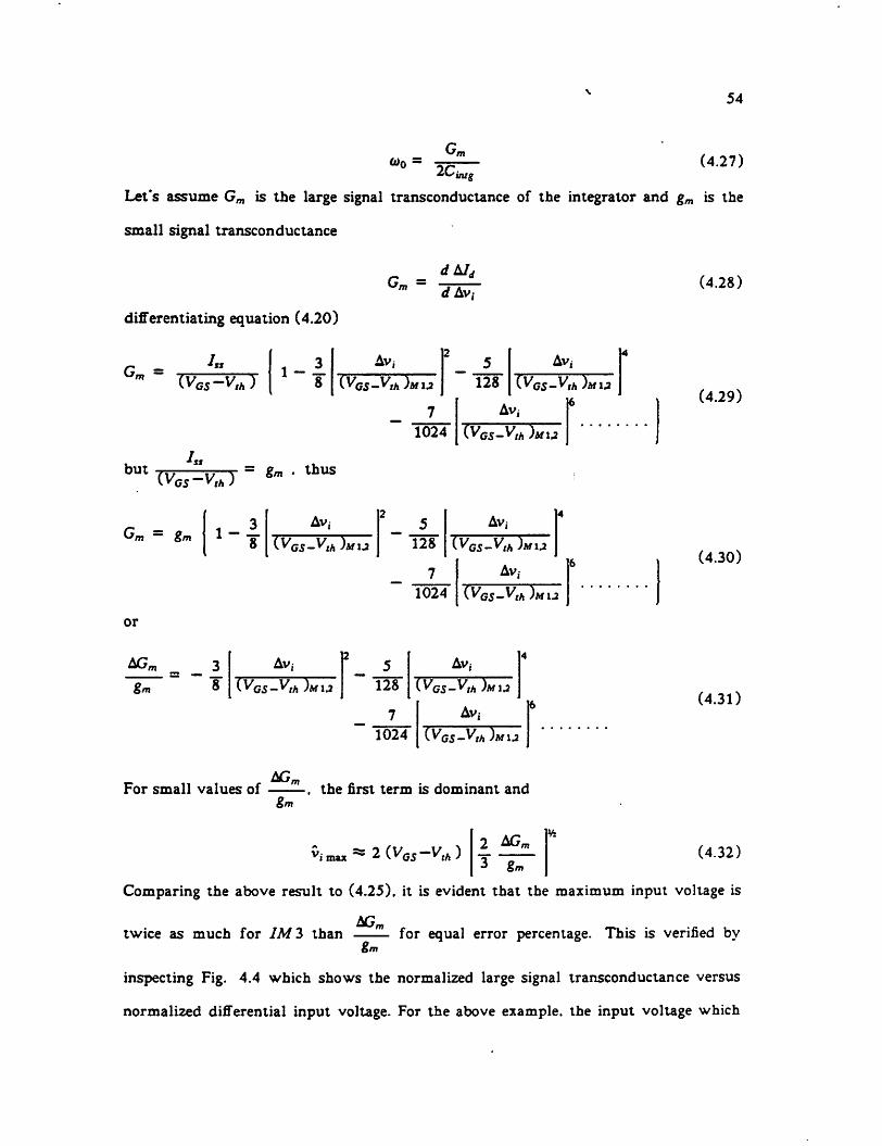
inspecting Fig. 4.4 which shows the normalized large signal transconductance versus
normalized differential input voltage. For the above example, the input voltage which
AV,
(V6S-V,h)M,,2
Figure 4.4
Normalized large signal transconductance of a source-coupled pairas a function of the differential input voltage.
55

resulted in IM 3 = 1% corresponds to — = 0.96gm
56
or a 4% shift in the center fre
quency of the filter. For the same example, a 1% center frequency shift occurs for
Vim«= 163 mV or viSMS = 115 mV (4.33)
4.2.13. Circuit Techniques to Improve the Integrator Linearity
Both equations (4.25) and (4.32) suggest that the upper limit of the output signal
could be increased by choosing large values for the input transistor gate overdrive
voltage.(VGS —Vth )Mlt2. The major limiting factor in this case is the maximum available
supply voltage. By inspecting equation (4.32). it is obvious that the worst case Q^g
and thus the maximum achievable filter quality factor, is proportional to
vI7T •' Therefore, achieving high Q with low passband error dictates low
values for (VGS —Vtn )MU. The above considerations suggests that the choice of the gate
overdrive voltage is based not only on maximizing the dynamic range, but also upon
the maximum power supply voltage and the filter quality factor.
Here a simple circuit technique is proposed to linearize the output current of the
integrator.
To compensate for the non-linearity of the output current, a cross-coupled
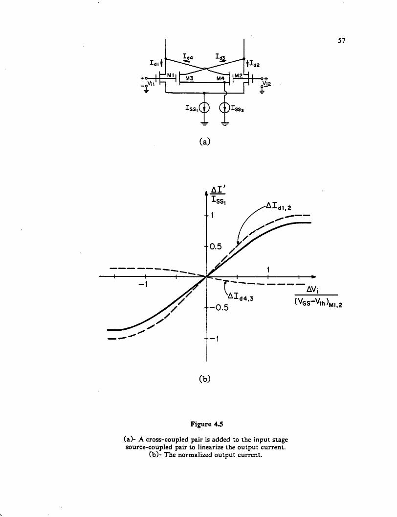
source-coupled pair is added to the input of the integrator (Fig. 4.5(a)) . The function
of the cross-coupled pair is to subtract a small amount of current. &Ldj4. which
becomes nonlinear more rapidly as compared to A/rf as shown in Fig. 4.5(b).
The total output current is given by
A/' = A/,u - A/,M (4.34)where A/rf is given by equation (4.20) and ^Idii is
♦I02
^t>
(a)
(b)
Figure 4.5
(a)- A cross-coupled pair is added to the input stagesource-coupled pair to linearize the output current.
(b)- The normalized output current.
57
(VGs-Vth)M|i2
A/,,. = /„33.4
Avj
(VG5-VrA )*,.«
Av,1
128 (VG5-VtA )**«
Avj
5
3
1
1024
Av,
(VGiS_V/A )af3,4
Let s assume that -=— = b and -^ r—r = a and thusiss 3 ^vG5—vxA;Af3>(<
It can be shown that
A/i3, = Iss iAv,
CVGJ-Vrt)«w
V-£-->A/3.4
Av,
(VG5-VrA )Wu
128
Av, 5 oi'6
58
(4.35)
(4.36)
(4.37)
Substituting from the above equation and (4.20) in (4.34) the total output current is
found
A/ = / Ml
l-iAv,
»-x
1
1281 -
Av,
The output current coefficients are given by
Av,
(VG5-V„JWU
10241 -
(4.38)
Av,
(VG5_VM )„,.;,
a-, =
1- a3
/»!
0
/„11 6 s (vG5 - vth y
Iss l•
128 (VG5 - vtny\
a3 = -
a5 = -
Using the derived values in (4.23)
IM3 =s ~^=-
a, = 0
a4 = 0
fi* = 0
3 1 X Av,2
32
>-TWGS-V,n)>
251 -
a5
10241 -
a
Av,
(VG5-VfA)MU
59
(4.39)
(4.40)
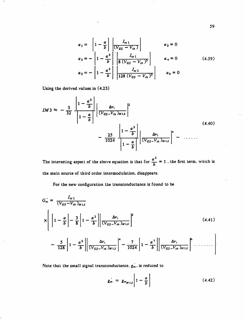
The interesting aspect of the above equation is that for -=- = 1 . the first term, which is
the main source of third order intermodulation. disappears.
For the new configuration the transconductance is found to be
Gm =<«i
(vGS-vtA)M
»-f
1281 -
«
»-VAv,
(VGs_VrA )«U
Av,
(VG5-VrA)wu 1024 *-vAv,
(VG5-Vrt)«u
Note that the small signal transconductance. gm. is reduced to
gm gr.'Mia J"T
(4.41)
(4.42)
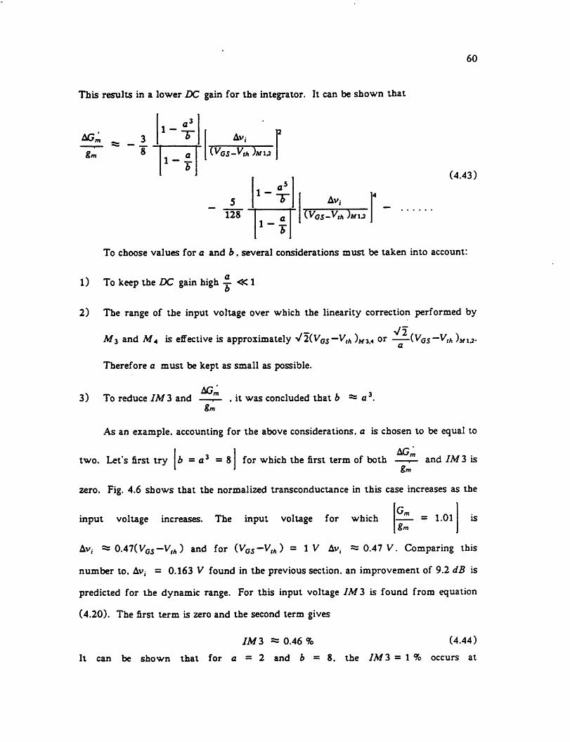
This results in a lower DC gain for the integrator. It can be shown that
AGm=s
3
8
1 T&m
>-f
Av,
(VG5-VrA )MUk
5
128
1-
»-x
Av,
(VG<5_VfA )wi.2
60
(4.43)
To choose values for a and 5. several considerations must be taken into account:
1) To keep the DC gain high i«lb
2) The range of the input voltage over which the linearity correction performed by
— -JoAf3 and MA is effective is approximately ^2(VGS—Vth )MZ4 or (VG5—Vth )MU.
Therefore a must be kept as small as possible.
AG^3) To reduce IM3 and —^- , it was concluded that b == a3.
gm
As an example, accounting for the above considerations, a is chosen to be equal to
AG,'two. Let's first try b =a3 =8 for which the first term of both and IM3 is
gr
zero. Fig. 4.6 shows that the normalized transconductance in this case increases as the
G,input voltage increases. The input voltage for which
gr= 1.01 is
Av, =s 0.47(VG5-V,A) and for (VG5-Vr„) = IV Av, ^ 0.41 V. Comparing this
number to. Av, = 0.163 V found in the previous section, an improvement of 9.2 dB is
predicted for the dynamic range. For this input voltage IM 3 is found from equation
(4.20). The first term is zero and the second term gives
IM3 *= 0.46% (4.44)
It can be shown that for a = 2 and b =8. the IM 3 = 1 % occurs at
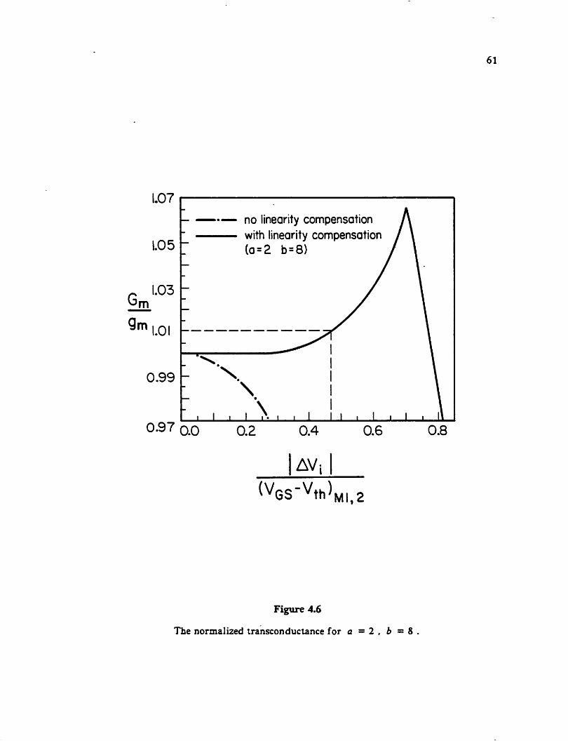
9m
L07
1.05
1.03
1.01
- — •— no linearity compensation—— with linearity compensation
(a =2 b =8)
0.99 \
\\
J I L
0-9? 0.0 0.2j^_i i
AV-,
(VGS"Vth)MI,2
Figure 4.6
The normalized transconductance for a = 2 . b = 8
61
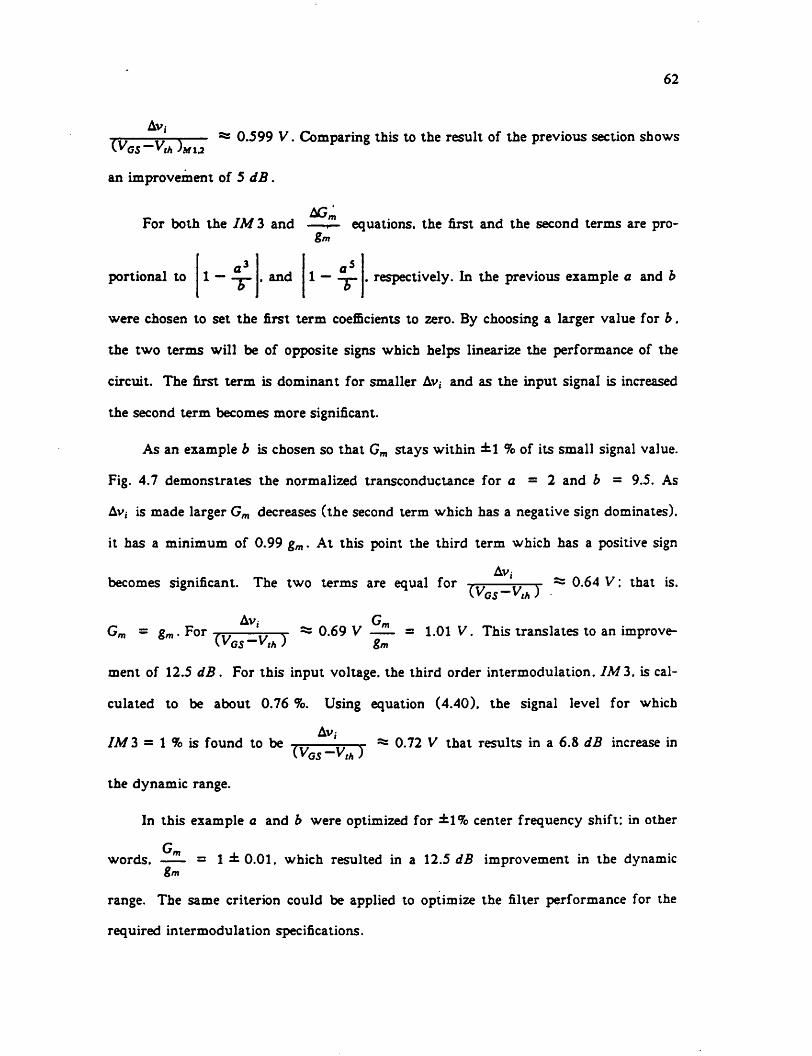
62
Av,ytj ^—r * 0.599 V. Comparing this to the result of the previous section showsv.VG5—Vtn )MXa
an improvement of 5 dB.
For both the IM3 and —r— equations, the first and the second terms are pro-gm
portional to 1 T . and -* . respectively. In the previous example a and b
were chosen to set the first term coefficients to zero. By choosing a larger value for b.
the two terms will be of opposite signs which helps linearize the performance of the
circuit. The first term is dominant for smaller Av, and as the input signal is increased
the second term becomes more significant.
As an example b is chosen so that Gm stays within ±1 % of its small signal value.
Fig. 4.7 demonstrates the normalized transconductance for a = 2 and b = 9.5. As
Av, is made larger Gm decreases (the second term which has a negative sign dominates),
it has a minimum of 0.99 gm. At this point the third term which has a positive sign
Av,becomes significant. The two terms are equal for -trr- r—r ** 0.64 V; that is.
tVG5—Vth )
Av, GmGm = gm- For -pr- ——r- == 0.69 V = 1.01 V. This translates to an improve-
\VGS—Vth) gm
ment of 12.5 dB. For this input voltage, the third order intermodulation. IM 3. is cal
culated to be about 0.76 %. Using equation (4.40). the signal level for which
Av,IM 3 = 1 % is found to be -rrr- ——r * 0.72 V that results in a 6.8 dB increase in
cvG5—vth)
the dynamic range.
In this example a and b were optimized for ±1% center frequency shift: in other
Gm .words. = 1 =0.01. which resulted in a 12.5 dB improvement in the dynamic
gm
range. The same criterion could be applied to optimize the filter performance for the
required intermodulation specifications.

.03
1.01
Gm
0.99
0.97
0.95
0.0
— no linearity compensation— with linearity compensation
(a=2,b=9.5)
(Vos-v,h)M,2
Figure 4.7
The normalized transconductance for a = 2 . b = 9.5
63
64
4.2.2. Distortion in the Filter Output Signal
As was mentioned earlier, the identical resonator filter architecture was adopted
for optimum sensitivity. However, due to the fact that the maximum signal of some of
the internal nodes of the filter is a factor of two higher than the output node signal
[14}. the maximum filter output with acceptable distortion is half the value found for
the integrator in the previous section. This results in a. 6 dB loss in the overall
dynamic range of the filter.
4.2.3. Noise Performance of the Integrator'
The equivalent input noise of the integrator can be calculated to be
v 2=v 2+v 2 +g* Mlfi
Mia
V * + V * (4.45)
where ve?Ml2 . v^ 2. ^eaM2 . veqM2 • are. the equivalent input voltage noise generators
of the input transistors and the load transistors, respectively.
Assuming that the lower band edge of the filter is at a much higher frequency
than the flicker noise "corner" frequency and therefore the contribution of this noise
component is negligible; the noise of all MOS transistors are thermal and
Vea2 = 4kT3«,
substituting in equation (4.45)
2 = SkT'*r 3 S™ Ml.
A/
1 +'m Af 7.8
8™ Mia
(4.46)
A/ (4.47)
Assuming " M1* = ~. the input referred noise spectral density of the integrator isgm Mli2
found to be

65
®m Mia
substituting for gm MU = 2o>0 C^g
5i(/)-=W!£- (449)It can be demonstrated that the same integrator implemented with operational
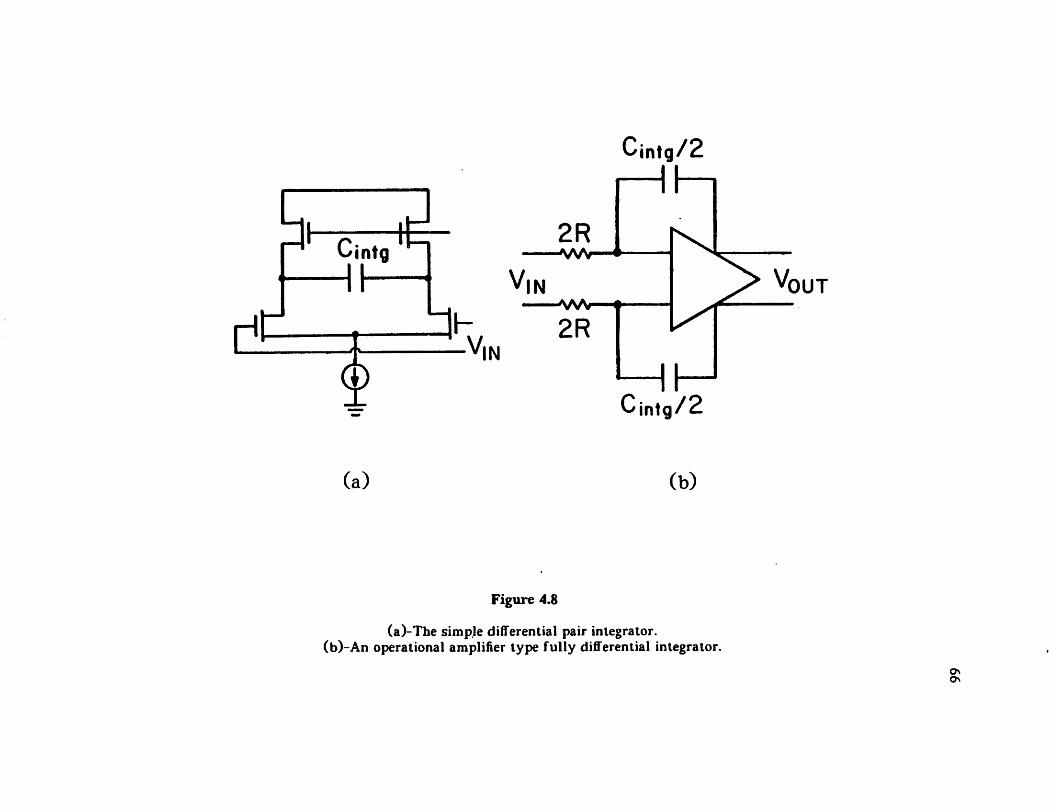
amplifier type fully differential integrators of Fig. 4.8 (b) would exhibit four times
more output noise power for equal total integration capacitance. This is due to the
bridge connection of the integrating capacitance as illustrated in Fig. 4.8 (a).
4.2.4. Noise Performance of the Filter
The total output noise power of a typical doubly-terminated sixth order ladder
bandpass filter implemented with identical integrators is found in Appendix B to be
v"Z7= 5, (/ )̂ X̂ L XQ%m X/ o (4.50)
where S, (/ ) is assumed to be frequency independent. / 0 corresponds to the center
frequency of the filter and {2£sm is the quality factor of the terminated resonators
which depending upon the desired shape of the filter frequency characteristics ranges
from one to two times the overall Q of the filter. Substituting for S,(/ ) and / 0 . the
total output noise power is found to be
, 2—7 *•* /-\term'out ~~ J 7?= 3^err (4.5D
intg
Since in recursive bandpass filters the output noise power is inversely proportional
to the integrating capacitor value, for the above integrator the noise can be drastically
reduced by choosing higher values for the integrating capacitors and paying a price in
terms of higher power consumption and die area. Whereas in switched-capacitor tech
nique the dependence of the operational amplifier settling time on the integrating capa-
(a) (b)
Figure 4.8
(a)-The simple differential pair integrator.(b)-An operational amplifier type fully differential integrator.
OUT
c*
67
citance limits the integrating capacitance to relatively small values for high frequency
filters. This in turn makes the achievement of low values of output noise easier in this
technique than in switched-capacitor filters.
43. Effect of Transistor Mismatches
The matching of the integrator transistors is an important factor to consider
because of the following reasons.
The matching of the unity-gain frequency. o>0> of all the integrators, which
directly affects the frequency response of the filter, is of particular importance. It can
be shown that the unity-gain frequency mismatch is given by
Aa0 AGm(M\a) bCtntg
m(Mia)
(4.52)'vug
In MOS processes the MOS capacitors can typically be matched within a few tenths of a
percent, whereas the MOS transistor transconductances matching is more difficult to
achieve. The mismatch of the input transistor transconductance from one integrator to
another is found to be
AGm(Mia) ^ 1
m(Mia)
*T>(£ +i
M12
**>
*
AV,th
(VG5-V,m(4.53)
AMO
MIO
The first two terms are geometry dependent and independent of bias point. The third
term is dependent on the threshold voltage mismatch and the gate overdrive voltage of
the current sources. M10. One way to reduce this term is by choosing a large value for
the current source gate overdrive voltage; as an example, a threshold mismatch of
LVth = 5 mV and (VGS —Vth )M 10 = 1 V results in 0.5% mismatch for o>0.
The second critical factor to consider, is the power supply rejection. PSRR. of the
integrator. For the circuit configuration of the designed integrator, the PSRR is strongly
68
dependent on the matching of the two input transistors. M1 and M 2. of each indivi
dual integrator [15].
The above considerations suggest that for both the unity-gain frequency matching
and PSRR improvement, the matching of the input transistors. Ml and M2. and the
current sources. M10, are more critical than the other integrator transistors. By physi
cally locating these devices close to each other better matching can be achieved. The
matching of the current sources threshold voltage can be substantially improved by the
use of common-centroid geometries [16].
4.4. Design of a 500KHz Filter
In this section, the studies performed in chapter 3 and chapter 4 are used to design
a sixth-order bandpass filter for an experimental prototype. The filter is designed for a
center frequency of 500 KHz and a quality factor of five.
The simplified circuit schematic of the filter is shown in Fig. 3.19. The filter is
chosen to have a chebychev characteristic with about 0.1 dB ripple in the passband.
The coupling coefficient and the termination quality factor are found from the
corresponding tables to be [10]
As discussed earlier, for the integrator design (Fig. 3.20). choosing a high
(VGS-Vth ^Mia) resu*ts in nigner dynamic range but lowers the intergrator Q. Thus,
considering the fact that the total power supply voltage is 10 V and there is a stack of
four transistors with threshold voltages of 1 V. the C^gs-Vm )(MU) was chosen to be
1 V. Table 4.2 is used to extract the optimum input channel length for
/ o = 500 KHz.
Lopt = 20/z (4-55)In section (4.2) it was shown that the output noise power of the filter is inversely pro-
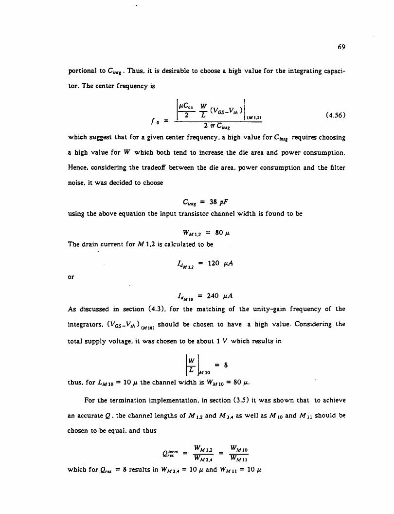
69
portional to C^. Thus, it is desirable to choose a high value for the integrating capaci
tor. The center frequency is
/o =
^*(V0S-V„,)iMia) (4.56)
2 irCuug
which suggest that for a given center frequency, a high value for C^g requires choosing
a high value for W which both tend to increase the die area and power consumption.
Hence, considering the tradeoff between the die area, power consumption and the filter
noise, it was decided to choose
Cinxg = 38 pF
using the above equation the input transistor channel width is found to be
Wmi.2 = 80/x
The drain current for M 1.2 is calculated to be
Id = 120 uAdMia *^
or
Id = 240 uAdM10 *•
As discussed in section (4.3). for the matching of the unity-gain frequency of the
integrators. (V*G5-.V*,A ){M10) should be chosen to have a high value. Considering the
total supply voltage, it was chosen to be about 1 V which results in
W_T
= 8IM10
thus, for LMi0 - 10 fi the channel width is WM10 = 80 fx.
For the termination implementation, in section (3.5) it was shown that to achieve
an accurate Q. the channel lengths of M\2 and ^3.4 as we^ as ^10 and M\\ should be
chosen to be equal, and thus
Qterm _ WM U = WM\0Wm3.4 WM i j
which for Qres = 8 results in WM34 = 10 ytx and WMU = 10 /z
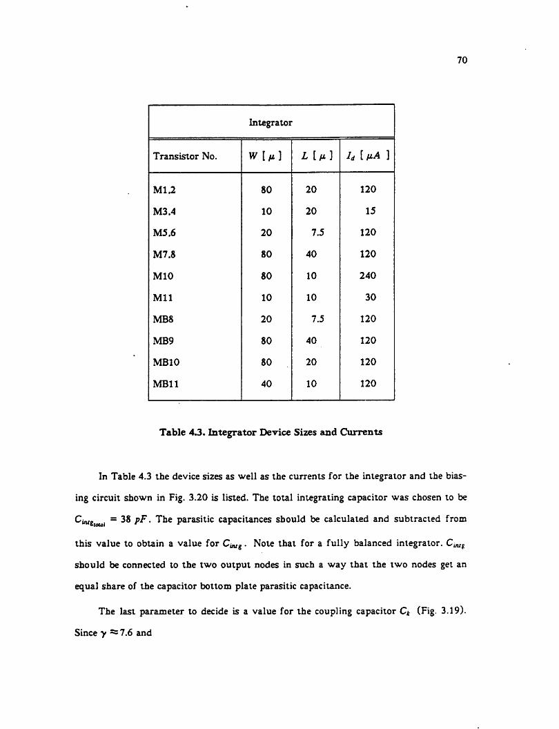
Integrator
Transistor No. win) L[fx] Id [ HA ]
Ml.2 80 20 120
M3.4 10 20 15
M5.6 20 7.5 120
M7.8 80 40 120
MIO 80 10 240
Mil 10 10 30
MB8 20 7.5 120
MB9 80 40 120
MB10 80 20 120
MB11 40 10 120
Table 4.3. Integrator Device Sizes and Currents
70
In Table 4.3 the device sizes as well as the currents for the integrator and the bias
ing circuit shown in Fig. 3.20 is listed. The total integrating capacitor was chosen to be
C^ = 38 pF. The parasitic capacitances should be calculated and subtracted from
this value to obtain a value for C^g. Note that for a fully balanced integrator. Cuug
should be connected to the two output nodes in such a way that the two nodes get an
equal share of the capacitor bottom plate parasitic capacitance.
The last parameter to decide is a value for the coupling capacitor Q (Fig. 3.19).
Since y ^=7.6 and
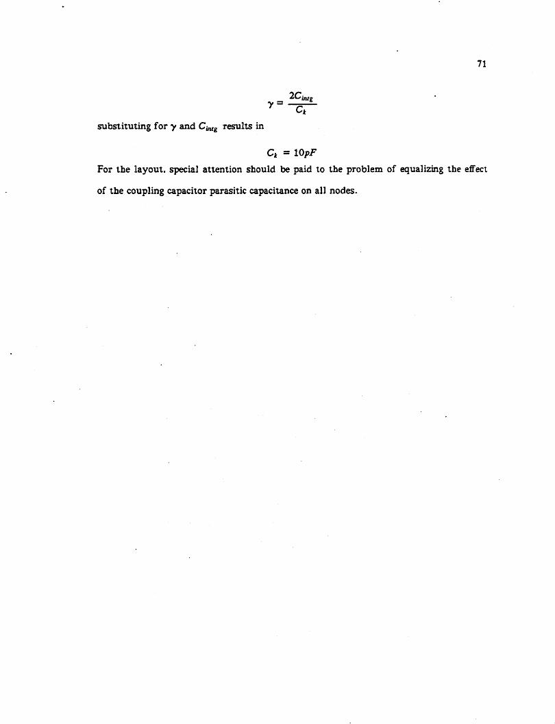
71
y= 2C™iCk
substituting for y and C^g results in
Ck = lOpF
For the layout, special attention should be paid to the problem of equalizing the effect
of the coupling capacitor parasitic capacitance on all nodes.
CHAPTER 5
CENTER FREQUENCY CONTROL CIRCUIT
As was mentioned earlier, the center frequency of continuous-time filters is
dependent on the absolute values of monolithic components. For the filter described in
chapter 3. these components are capacitors and transistors transconductances which are
both temperature and process dependent. Thus, the center frequency must be either
tuned externally or some extra circuitry should be added to eliminate the necessity of
the external tuning. To overcome this problem a modified version of the phase-locked
loop scheme, introduced by Gray and Tan in 1977. is proposed and described in this
chapter.
5.1. The Modified Phase-Locked Loop Concept
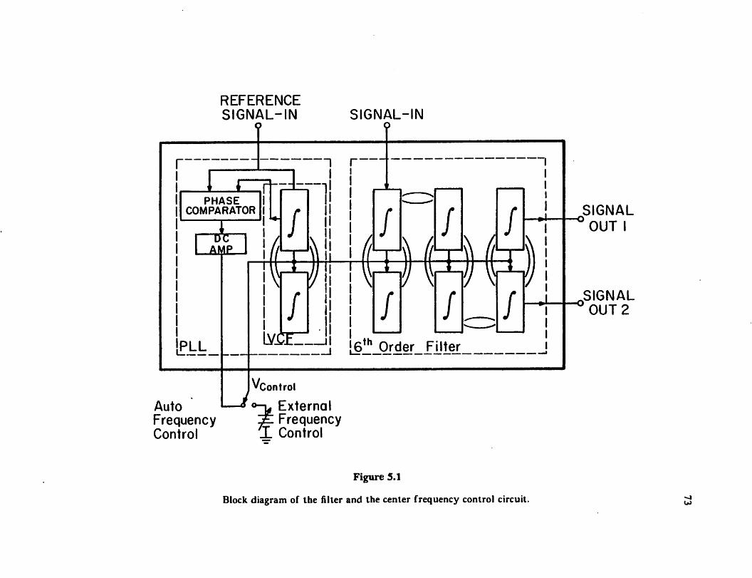
Figure 5.1 shows the block diagram of the filter and the center frequency control
circuit. The center frequency can either be controlled through an external voltage
source or an on-chip phase-locked loop locks the center frequency to an external refer
ence frequency. The phase-locked loop differs from the conventional PLL as it utilizes
an exact replica of the main filter's second order section (voltage controlled filter. VCF)
instead of the conventional voltage controlled oscillator, or VCO. The reason for this
modification is that the realization of a CMOS VCO with stable center frequency at
KHz and MHz range is quite complicated. It will be proven that the maximum error
due to this is negligible.
The phase detector compares the phase difference 4> between the input and output
of the filter and generates an error voltage proportional to the phase difference. The
error voltage is then amplified and used to change the center frequency of the filter in a
direction which reduces the difference between the two frequencies.
72
REFERENCESIGNAL-IN
cPHASE
COMPARATOR
AM£.
SIGNAL-INo
/ /
/ /
/
¥mi
[PLL ly£E—il !6,h Order Filter
AutoFrequencyControl
U^Control
°-u External'jL FrequencyX Control
Figure 5.1
Block diagram of the filter and the center frequency control circuit.
SIGNAL
SOUT I
^SIGNALOUT 2
74
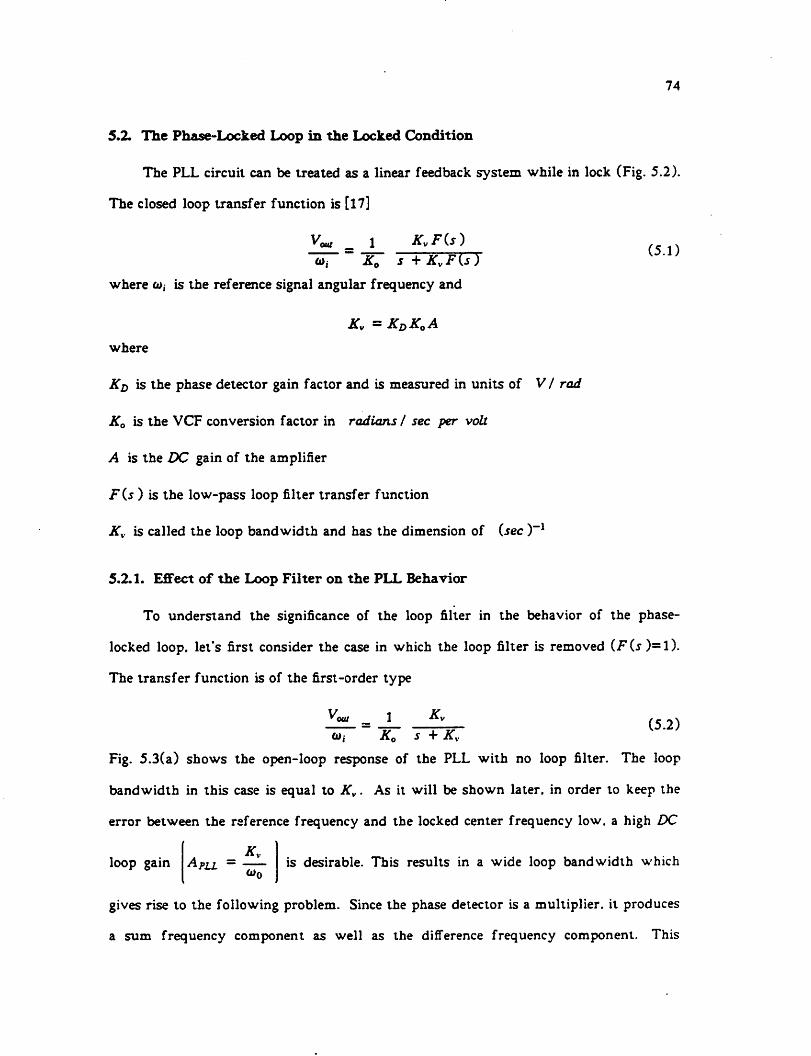
5.2. The Phase-Locked Loop in the Locked Condition
The PLL circuit can be treated as a linear feedback system while in lock (Fig. 5.2).
The closed loop transfer function is [17]
Vo«___l_ KvF(s)co, ~ K0 s + KvF{s)
where to, is the reference signal angular frequency and
Av = KqKqA
where
KD is the phase detector gain factor and is measured in units of V / rod
K0 is the VCF conversion factor in radians I sec per volt
A is the DC gain of the amplifier
F(s ) is the low-pass loop filter transfer function
Kv is called the loop bandwidth and has the dimension of (sec )-1
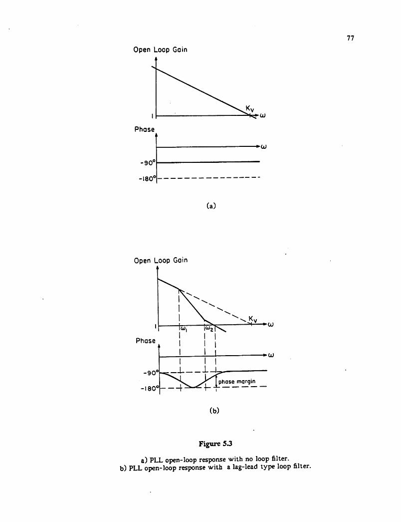
5.2.1. Effect of the Loop Filter on the PLL Behavior
To understand the significance of the loop filter in the behavior of the phase-
locked loop, let's first consider the case in which the loop filter is removed (F (s )= 1).
The transfer function is of the first-order type
"out __ 1 "**v r- -•»
~' #7 s +kvFig. 5.3(a) shows the open-loop response of the PLL with no loop filter. The loop
bandwidth in this case is equal to Kv. As it will be shown later, in order to keep the
error between the reference frequency and the locked center frequency low. a high DC
A\.loop gain ApLL = —
<D0is desirable. This results in a wide loop bandwidth which
gives rise to the following problem. Since the phase detector is a multiplier, it produces
a sum frequency component as well as the difference frequency component. This

Reference Signal
k
t i1 ii i
r
Multiplier
KD [v/Rad]Voltage
Controlled
Filter
<—
y f k [Rad/seclo L V
DC Amp &L.P. Filter
A Ps)
i l
i f i •
V
Figure 5.2
Block diagram of PLL system.
Control
75
76
unwanted component which is at twice the reference frequency plus all interfering sig
nals present at the input will appear at the output. Thus, a low-pass loop filter is
required to filter out these unwanted signals.
One filter configuration which lowers the bandwidth of the loop while maintaining
enough phase-margin to ensure stability is [18]
1 + -L
F(s) = ?L (5.3)1 + JL
where ci>i corresponds to a pole at a frequency much less than Kv and results in an
additional 90 degree phase shift as shown in Fig. 5.3(b). To increase the phase margin, a
left half-plane zero. a>2. is added in the loop filter at a frequency close to the cross over
frequency.
By using the loop filter, the loop bandwidth and the DC loop gain can be set
independently.
5.2.2. Error Between the Locked Frequency and the Reference Frequency
The major drawback to the modified PLL. which utilizes a voltage controlled filter
instead of the conventional voltage controlled oscillator, is that there exists an error
between the locked center frequency. / £e4erf. and the reference frequency. fref . which
tends to increase as the difference between the unlocked center frequency. / %,lockeJ , and
the reference signal is increased. It can be shown that
f unlocked _ r
fr- = /„/ +^—.—i^L (5.4)For a conventional phase-locked loop, the following equation is always true while in
lock
/fr*" = fref (5.5)whereas for the modified PLL the above equation is true only when f™locked = f rtf .
Open Loop Gain
Phase
-90°
-180°
Open Loop Gain
Phase
•+-0U
(a)
(b)
Figure 53
a) PLL open-loop response with no loop filter,b) PLL open-loop response with a lag-lead type loop filter.
77
78
By choosing high values for APLL . the error can be kept within acceptable limits: as an
example for a capture range of ±15% and loop gain of 300. the maximum error is only
0.05% of the center frequency which in most cases is tolerable.
53. The Phased-Locked Loop Building Blocks
In this section the design of the building blocks of the PLL on the circuit level is
discussed.
53.1. Phase Comparator Design
The phase comparator configuration is chosen to be a CMOS version of the Gilbert
four-quadrant multiplier circuit as shown is Fig. 5.4 [20]. The bias circuit for all PLL
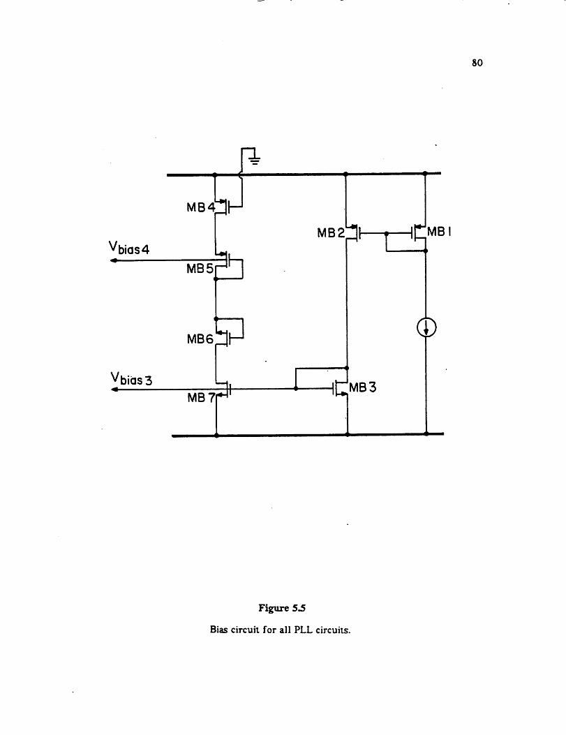
circuits is demonstrated in Fig. 5.5.
The small signal differential output current of this circuit is found to be [19]
1*
A/0 = fiQ
The differential output voltage of the multiplier is given by
I L MP1.2 L MP3.4.S.6
AV0 =A/0r0
To find the phase detector gain. KD, let's assume
V« l (* ) = Vpi, sina*and
Vin2(0 = Vpk 2sinbot +<j>)substituting for V^ 2 and V* 2 in (5.6)
VinMin2 (5.6)
(5.7)
(5.8)
(5.9)
AV0 = fiC0 id) (Z)2 L MPia L MPiA.s.6
r0 Vpk J sinour Vpk asin(o>r +0) (5.10)
or
AV =2
f*C0
1 L, MP\a L Af/»3.4,5,<Sr0V.'pkx VpXjjCos4> + cos(2o>* +0) (5.11)
As the above equation suggests, the output voltage consists of a DC component which

Vbias 4
Reference
Signal
From Filter Output
Vbias 3
Figure 5.5
Bias circuit for all PLL circuits.
To Amplifier
NO
Vbias 4
Figure 5^
Bias circuit for all PLL circuits.
80
81
is a function of the phase difference between the two signals and an AC component at
twice the original frequency. The AC component is filtered out by the loop low-pass
filter and the average output voltage AV0 is given by
v>
AVaMCfl
"average 2 L MP\a L MP3,4,5,6roVMlV„i2cos0 (5.12)
7TNote that AV0 is at it's maximum for <f> = 0 and 4> —ir and AV0 = 0 for <f> = ~ . But
7Tcos0 = sin (-5- —(f>)
and for 0 close toir
COS0 = (-=- —0)
Substituting (5.14) in (5.12)
AVnaverage
To find Aj>
differentiating (5.15) gives
where r0 is given by
2 L MPX2 L MP1.4J&.6
Kn =dAV0
d<j>
roVptivPk2 (2V
2 L MPU L MP3.4.S.6
Vi
r*v*lv*>
r0 =2
Imp u
(5.13)
(5.14)
-0) (5.15)
(5.16)
(5.17)
(5.18)
53.2. Voltage Controlled Filter
The VCF is chosen to be the exact replica of the main filter's second order section
for matching purposes. Fig. 5.6 shows the flow-graph of the filter. The transfer func
tions of the two outputs are given by
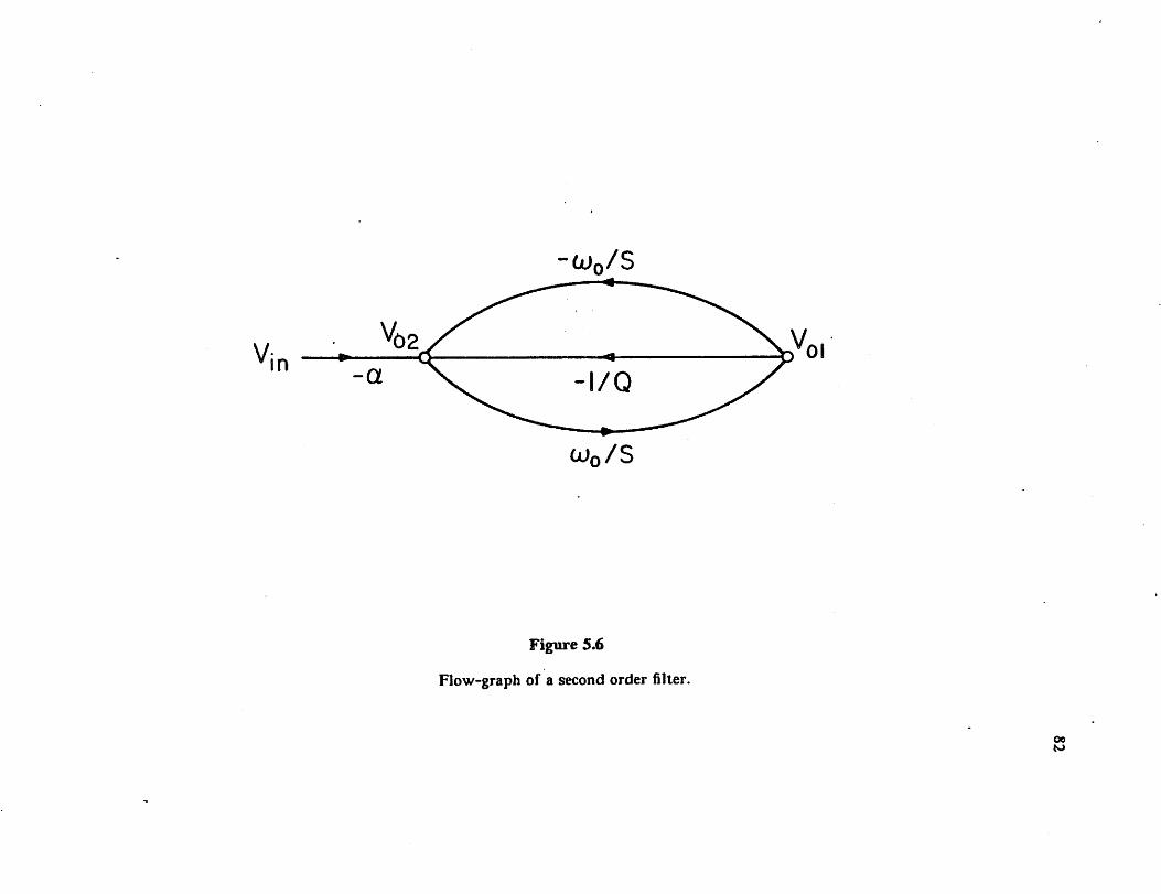
-(jjn/S
OJn/S
Figure 5.6
Flow-graph of a second order filter.
Ooto

%=
—
s— a
"in S2
too"+
5 .
tooG+ 1
V°2—
s2—w- a
too
83
(5.19)
, (5.20)4+ * +1a>o tooG
The bandpass output. v0j. has a 180 degree phase shift at the center frequency (s=j<o)
with respect to the input signal. The second output. v02. has a high-pass characteristic
with a peaking at the center frequency and a —90 degree phase shift at this frequency.
Considering the phase-detector characteristics. v02 seems to have the desirable phase
response to generate the error voltage. Fig. 5.7(a) shows the amplitude and phase
response of v0 . To verify that choosing v02 as the input to the phase detector does
indeed produce a suitable error voltage for center frequency control, the DC component
generated by the multiplication of vin and v0 which turns out to be equal to
'j*«v/*« cos^ (5.21)
is shown in Fig. 5.7(b) . The error voltage is zero for / = / 0 and is at its maximum
for / = / 0(l± -=75-). Note that this corresponds to the error voltage when the loop is
broken. Once the loop is closed, this voltage changes the center frequency of the filter
and reduces the difference between the two frequencies.
In this part the VCF gain. K0. which is defined as the variation of the center fre
quency in response to the output voltage of the DC amplifier, is found. Fig. 5.8 shows
the circuit diagram of the VCF and the voltage to current converter. Note that K0 also
includes the contribution of the voltage to current converter
Since
*0 =^ (5.22)dv,
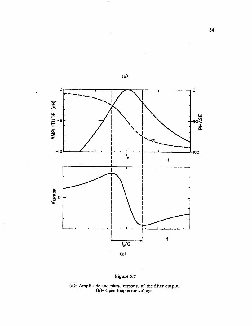
Figure 5.7
(a)- Amplitude and phaseresponse of the filter output,(b)- Open loop error voltage.
84
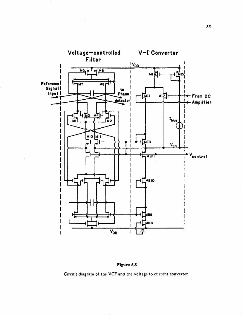
Reference
SignalInput
Voltage-controlled V-I ConverterFilter
'VD0
Figure 5.8
Circuit diagram of the VCF and the voltage to current converter.
85
From DC
Amplifier
control
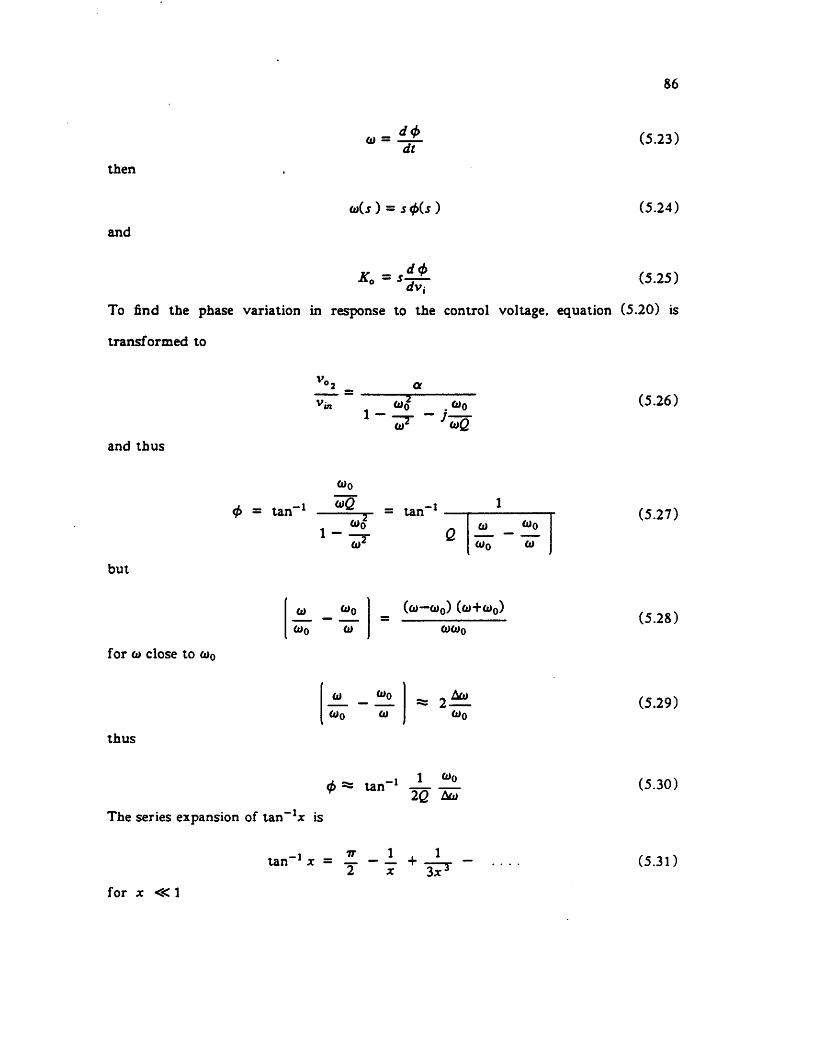
then
and
and thus
but
for to close to to0
thus
d4>to = —2-
dt
to(s ) = s <f>(s )
86
(5.23)
(5.24)
*-*'*<fVi
(5.25)
To find the phase variation in response to the control voltage, equation (5.20) is
transformed to
-l
to0
toQ
to©* _ . to0to2" ;to<2
t-i<f> = tan 7
Qto __ too
or to0 to
cd to0 (to—to0) (to+to0)to0 to toto0
cj too
to0 toss ? ^
to0
0 =s tan * —- -j—^ 2Q Ato
(5.26)
(5.27)
(5.28)
(5.29)
(5.30)
The series expansion of tan 1x is
for x <3C1
tan f x = — — — + —2 x 3x
(5.31)
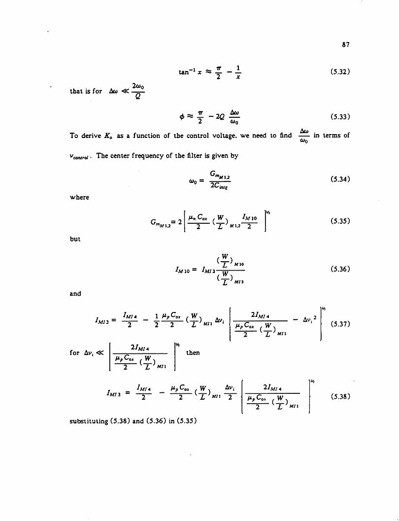
2to(that is for Ato «
♦ -l - v 1tan 'x *- - —2 x
2 to0
87
(5.32)
(5.33)
AtoTo derive K0 as a function of the control voltage, we need to find in terms of
"too
vcoruroi • The center frequency of the filter is given by
where
but
and
Af/3 -A//4
G»MU" 2
to0 ="AfU
2Cinxg
Mn Cox , W x Af 102 T" mu~~2~~
(-151)
A-v L Mn
Af 10 = Af/3
1 UpCo* , w. .2 2 L Mn
2/^/4
2 i, ""
2/m/4for Av, «
2 JL *n
then
Af/4 _ VPC0X JV Avi 2/M/4
- Av,
fA/7 3 2 xX'*/i 2 /xPCoa f\y^2 £ *«»
substituting (5.38) and (5.36) in (5.35)
(5.34)
(5.35)
(5.36)
(5.37)
(5.38)

'AfU
MnC0X W, (*)1M14 f*pCox w. A^
L'*1" 2
88
(5.39)
2/M/4Vi
V-pCox ,w.L Mn
For Avj = 0 . the filter center frequency is at its initial, unlocked value (to0 = ^o^^, )•
Considering this and equation (5.34) and (5.39) . it can be found that
to0 - to0matal
1 - 2Av,
for small Av,
Wo % to0. 1 - Avi
or
to0
<*>o ^Av<
outial
VPC0X yy2 L un
21MI 4
f*pCox W_2 L Mn
21Ml 4
rlpCox ,W2 L Mn
21MI 4
Vs
by manipulating the above equation and setting <*>o "" to0 , = Ato
Ato ^
tootnatal
M,C
Av,(*)
2 L Mn
21MI 4
Substituting the above equation in equation (5.33) gives
<t> *= y - 2Q Av, 2 L Mn
21Ml4
(5.40)
(5.41)
(5.42)
(5.43)
(5.A4)
The VCF gain is found from differentiating the above equation and substituting in
equation (5.25) then
K0 = 2Q to
HPC0X W.2 L MJ1
21MI 4
89
Vt
(5.45)
Note that the VCF gain is directly proportional to the filter quality factor. The term in
the brackets is equal to srrrj rr—? . This suggests that to achieve a high gain, a
low gate overdrive voltage for Ml 1 is required.
53.3. DC Amplifier Design
The DC amplifier is chosen to have a simple one stage configuration. Fig. 5.9
shows that the phase detector output is directly connected to the P-channel input
transistors and the same signals are level shifted and applied to the N-channel input
transistors, in order to have all four transistors operate in the saturation region. The
common mode output voltage is stabilized by MA 5 and MA 6 which operate in the
triode region.
The gain of the amplifier is given by
&m(MA\X> 8m{MA2.4)A =
£°(AM1.2) £° MA 3.4)
Substituting for gm(MAl2y fr-uMM)' &Hma^Y *<><imm>
A =^MA 12 + ^MA 3.4
or
Mn Cox yy
2 L MA 1.2
Vi
IMAI
Up cox yy,2 L MA 3.4
A =77
1 + *
-MA 12 -MA 3.4
(5.46)
- (5.47)
(5.48)
From the above equation it is evident that to achieve a large gain, the transistors
MA 1.2 and MA 3.4 should be chosen to have long channel lengths while the gate over-

FROM ^PHASE DETECTOR
PLL COMPENSATION
vbias 3
i_iiMA8
Ccl
AMPLIFIER
Figure 5.9
DC amplifier and the loop filter.
TO+ V-I
CONVERTER
o

91
drive voltages (VGS_VrA ) must be chosen to be low. On the other hand, for the PLL to
be able to handle relatively high signal levels, high (VG5«VtA ) is required. The choice of
transistor channel lengths is limited by the fact that larger size transistors have higher
parasitic capacitance which results in the degradation of the PLL phase margin. These
considerations must be accounted for the design of the amplifier.
53.4. Loop Filter
The loop filter consists of CcX . Cc2 and MAS . MA9 (Fig. 5.9). It performs as a
lag-lead type filter which generates a pair of left-hand plane pole and zero. The com
pensation capacitor CcU is Miller multiplied and the frequency response of the loop
benefits from the pole-splitting effect of this configuration [16] . The dominant pole is
located at
(X)'poit r0mutlA Ccl2 (5.49)
where A is the amplifier DC gain and is given by equation (5.47) and r0 is given by
"mutt
to,
^A/P9.10 + ^MP3.4.5.6
The pole location of the loop filter controls the bandwidth and thus, the capture range
of the PLL. Hence, the value of Ccu is dictated by the desired capture range.
The zero is located at
1
1 1
'MP 11
8°MA 8.9 &m(MA U) &m iMA 3.4)
W
(5.50)
ratio is chosen so that
(5.51)
MA& and MA? operate in the triode region and the
g °MA 8.9<K &m(.MA\3) &m(MA*.4) This causes the right half plane zero, due to the direct
propagation of the signal through the compensation capacitor, to move into the left
hand plane to improve the loop phase margin. The zero location can be approximated

92
by
—2— "7~ ^ G5 *w'AM 8.9 (5.52)
Qtrm ^ —cc 12
As mentioned earlier. Cc\2 is determined by the pole location and the desired zero loca
tion is achieved by the proper choice of
2 L MP\2 L MP 3.4,5.6
Vt
Kn =IT
The VCF gain was found as
WTo compensate for process varia-
' JAM 8.9
tions the zero location can be controlled externally by changing the gate voltage of
MA 8 and MA 9.
A significant source of extra phase shift, which can result in instability, is that
^control flas to drive a relatively high capacitance (in this case eight current source
transistor gates). To overcome this problem gmMIi must be chosen to be sufficiently
high.
5.4. Analysis of the Monolithic Phase-Locked Loop
In the previous section, the PLL building blocks were designed and analyzed. In
this section the overall behavior of the PLL will be evaluated. This is best achieved by
analyzing the PLL portion of the experimental prototype.
In Table 5.1 the device sizes chosen for the prototype as well as the drain currents
are listed. The process parameters of Table 4.1 are used for all the calculations.
First the phase comparator gain is calculated by using equation (5.17) and (5.18)
T Q
l^MPl 1*MP9
It is assumed that Vpk i = V*^ 2 = 100 mV thus
KD «= 0.224 V/ rod
7^77^'^ (5.53)
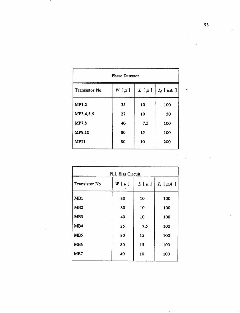
Phase Detector
Transistor No. W[fi] Ll/i] h [ M 1
MP1.2 35 10 100
MP3.4.5.6 27 10 50
MP7.8 40 7.5 100
MP9.10 80 15 100
MP11 80 10 200
PLL Bias Circuit
Transistor No. Wl/i] L [fi] h [ tiA )
MB1 80 10 100
MB2 80 10 100
MB3 40 10 100
MB4 25 7.5 100
MB5 80 15 100
MB6 80 15 100
MB7 40 10 100
93

Voltage to Current Converter
Transistor No. W[fi) L[fi) U i y-A )
Mil.2 60 7.5 300
MI3 100 10 300
MI4 390 10 600
MI5 130 10 200
DC Amplifier
Transistor No. W[fi] L [fi] h [ fJ-A ]
MA1.2 80 15 100
MA3.4 80 15 100
MA5.6 25 7.5 100
MA7 80 10 100
MA8.9 10 40
Table 5.1. Device Sizes and Current Levels for PLL Building Blocks
K0 = 2Q to
y-p Cox , W^ L a"1
21Ml4
The designed second order filter has a quality factor of eight thus
K0 2= 5 to0 rod I V —sec
v%
94
(5.54)

The DC amplifier gain is given by equation (5.47) as
A =2 L MA 12
Vi
6* _+ «, <MA7
substituting for the parameters
Thus the open loop gain is given by
A *s 280
Kv = KD KQ A =2 320 too
and the DC open loop gain is found to be
Substituting for ApLL in (5.4)
APLL = — = 320to0
f*p Cox W.2 L AM 3.4
/locked — f •0 — J ret +
/ unlocked _ /7 0 7 "/
320
95
Vi
•(5.55)
which results in an extremely small error between the locked center frequency and the
reference frequency.
In this part the open-loop frequency response of the PLL is analyzed to ensure the
stability of the loop.
The center frequency of the designed filter is at / o = 500 KHz thus
Kv *r 320 to0 = \CHz
The loop filter singularities are found by using equations (5.49) and (5.52).
<*>pol< -\^MP9.10 + ^MPZA.S.bUtMP11
(5.56)A CcU
Cc 12 was chosen to have a value of 50 pF. therefore
f pole * ""22 Hz
and
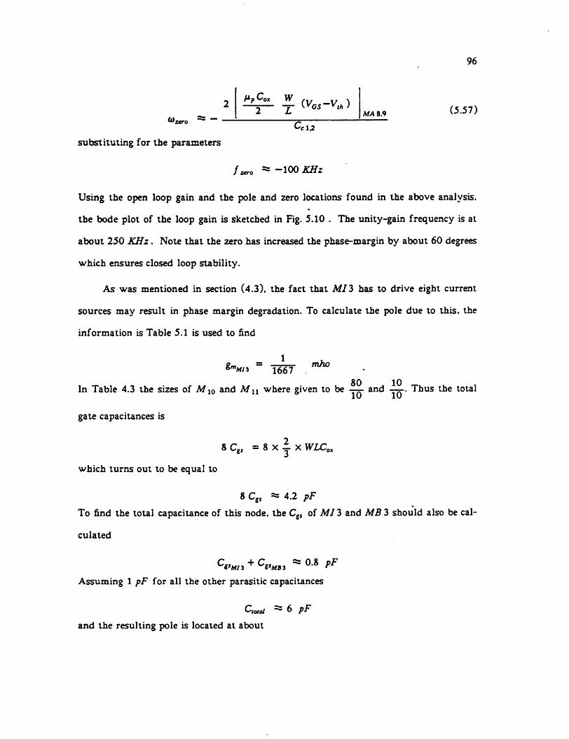
2
to^-n as — —
gate capacitances is
96
AM 8.9 (5.57)
Ccl,2
substituting for the parameters
fzero ** -100 Jtff2
Using the open loop gain and the pole and zero locations found in the above analysis,
the bode plot of the loop gain is sketched in Fig. 5.10 . The unity-gain frequency is at
about 250 KHz. Note that the zero has increased the phase-margin by about 60 degrees
which ensures closed loop stability.
As was mentioned in section (4.3). the fact that Af/3 has to drive eight current
sources may result in phase margin degradation. To calculate the pole due to this, the
information is Table 5.1 is used to find
2m = —rr-=- mho
In Table 4.3 the sizes of M10 and Mn where given to be — and —r-. Thus the total
8Cgs =8X1 XWLC0Xwhich turns out to be equal to
8 Cgi =* 4.2 pF
To find the total capacitance of this node, the Cgs of Ml 3 and MB 3 should also be cal
culated
Assuming 1 pF for all the other parasitic capacitances
Ctoial ^ 6 pF
and the resulting pole is located at about
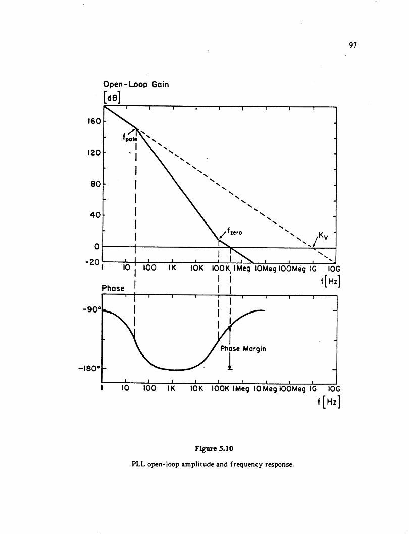
Open-Loop Gain
10 100 IK IOK lOOK IMeg lOMeg IOOMeg IG lOG
f[H,]Phase
-180°-
10 100 IK IOK lOOK IMeg 10Meg IOOMeg IG lOG
f[H«]
Figure 5.10
PLL open-loop amplitude and frequency response.
97
98
fp* =-^- * 16 MHzwhich results in about 1 degree extra phase shift at the unity-gain frequency of the
open-loop gain.
In the next chapter, the experimental results of the PLL analyzed in this section
are presented.
CHAPTER 6
EXPERIMENTAL RESULTS
In this chapter, the results from an experimental prototype are presented. A
sixth-order bandpass filter with an on-chip center frequency control phase-locked loop
with a center frequency of 500KHz and a quality factor of five was designed and
fabricated. The design of a bandpass filter with the above specifications was discussed
in chapter 4 and the phase-locked loop was explained in chapter 5. Fig. 6.1 shows the
microphotograph of the experimental chip. A 6—micron single-poly n-well CMOS
technology was used and the die area is about 4mm2.
In Fig. 6.2(a) the overall frequency response of the filter is shown. The detailed
passband of the two different outputs of the filter is seen in Fig. 6.2(b). The frequency
response of the filter is very close to the shape simulated with the program SPICE and a
± 10% variation in the power supply voltage produced no significant change in the filter
frequency response.
The functionality of the PLL is shown in Fig. 6.3, note that the markers are added
externally to indicate the reference frequency. First a reference frequency at ASOKHz
is applied, the filter frequency response locks to this frequency. Then the reference fre
quency is changed to SOOKHz, the filter follows this change. The last curve is for a
reference frequency at 550KHz. This corresponds to a 20% lock range for the phase-
locked loop.
The maximum output voltage with acceptable distortion is measured in Fig. 6.4 .
The measurement is performed for 1 % third order intermodulation distortion. 1M 3.
The output voltage for this condition is about 300 mVF—P or 106 mVrms. The max
imum output voltage for the integrator was calculated in section (4.2.1.1) to be99

Figure 6.1
Microphotograph of the experimental chip.
100

-6
dB
-31
-56 -
-5
dB
-to
-15 -
300
mm
440
500
KHz
(a)
500
KHz
(b)
700
Esftttmm
560
Figure 6.2
(a) -Overall frequency response of the prototype.(b) -Detailed passband of two outputs of the filter.
101
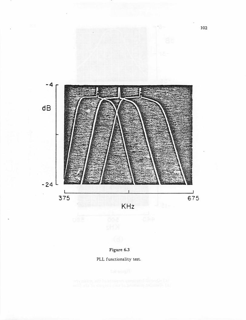
4 r
dB
-24 -
375
KHz
Figure 6.3
PLL functionality test.
102
675

-6
[dB]- 26
-46 _W
325
1111innmilmnmill..__.
iiiesej^i
HIE23Ha
500
KHz
Figure 6.4
Maximum output voltage for IM 3 = 1%.
103
675
104
230 mV. Considering the fact that for the identical integrator filter architecture there
exits a 6 dB loss in the dynamic range (section 4.2.2). the theoretical maximum voltage
turns out to be about 115 mVrms which is consistent with the measured 106 mVrms.
The total in-band noise is found from Fig. 6.5 to be about 30^tVrms for a
bandwidth of 96KHz. In order to compare the experimental noise to the theoretical
noise, the prototype values of C^g = *&Pf and Or* = 8 are substituted in equation
(4.51)
^inxg
which gives a total output noise of 50fiVrms. Note that the experimental value is for
the total "in-band" noise whereas the calculated value includes noise over the whole
frequency range. The results are reasonably consistent considering the fact that most
of the noise power falls within the passband of the filter. The center frequency of the
filter was controlled externally for the noise measurement. The reference signal feed-
through at the output of the filter was measured by controlling the center frequency
through the phase-locked loop. As can be seen in Fig. 6.6 the feed-through is about
100 fiVrms which exceeds the output noise and degrades the dynamic range by lOdB .
The relatively high reference signal feed-through is partly due to the fact that for
debugging purposes, some extra nodes were connected to bonding pads which increased
the parasitic couplings. Another reason for this is due to some asymmetry in the filter
layout.
Using the above measurements the dynamic range of the filter could be calculated:
For the stand-alone filter (external center frequency control), the dynamic range is
found to be
. » 100 mV ,n . ,DDynamic Range = -^—p- = 70.0 at5
The dynamic range of the filter while controlled by the PLL. is determined by the
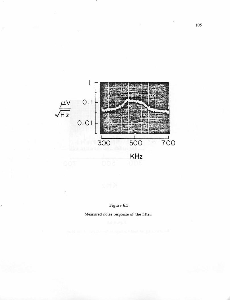
/iV 0.
0.0
300
Figure 63
Measured noise response of the filter.
105
700

100 ^V
lO^tV
L
prFn-Ti,i,,i,!"i,i.ii;'.,Tr.'Ti'TO..i.L",j.,,jiiiL!jm!!mii.iiiiiiii.i.-,'i»w:wr»iw,pwiw,**li|jjjui •Utilllulii.LlnlJj iuiiiiliiJkULkili
_J I300 500 700
KHz
Figure 6.6
Reference signal feed-through to the output of the filter.
106

107
reference signal feed-through rather than the output noise.
Dynamic Range - —?-:—=-r = 60 dBJ 6 100 fiV
The power supply rejection for both supplies is measured from Fig. 6.7(a) and Fig.
6.7(b) and is better than 35dB . The common mode rejection of the filter is tested by
applying the same signal to the two differential input of the filler and monitoring the
output. As Fig. 6.8 shows, the common mode rejection is about —45 dB within the
passband of the filter. It is believed that a perfectly symmetrical layout and a better
component matching should improve both the common mode and power supply rejec
tion and the reference signal feed-through.
In Table 6.1 the results for the sixth order bandpass filter for 10V supply voltage
is summarized.

dB
700
dB
700
Figure 6.7
Power supply rejection with respect to the positive and negative supply.
108

-5 r
dB -45 •
-8 5
300 500 700
KHz
Figure 6.8
Common mode rejection measurement.
109
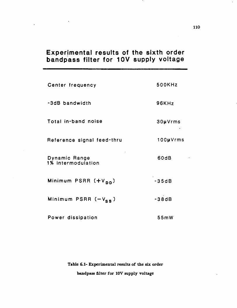
Experimental results of the sixth orderbandpass filter for 10V supply voltage
Center frequency 500KHz
-3dB bandwidth 96KHz
Total in-band noise 30HVrms
Reference signal feed-thru "lOOuVrms
Dynamic Range 60dB1% intermodulation
Minimum PSRR (+ VDD) -35dB
Minimum PSRR C-Vss) -38dB
Power dissipation 55mW
Table 6.1- Experimental results of the six order
bandpass niter for 10V supply voltage
110
CHAPTER 7
CONCLUSION
A design approach to implement high-frequency continuous-time filters was
presented. From the experimental performance of the filter it can be concluded that
this technique is indeed a viable method for the implementation of high-frequency
filters.
The problems hindering the extension of the low-frequency frequency-locked
filtering techniques were overcome by 1) using a simple circuit configuration for the
integrator design and utilizing the phase error cancellation technique. 2) Modifying the
conventional phase-locked loop scheme for controlling the center frequency of the
filter. Instead of the VCO a voltage controlled filter. VCF. was utilized. Detailed
analysis proved that the error due to this is very small. 3) Fully differential architec
ture was employed to improve the power supply and common mode rejection and thus
minimized the reference signal feed-through to the output of the filter.
The fundamental limitations of this approach were studied in chapter 4. In
Fig.7.1 the capability of this technique in a scaled technology is projected. Here the
maximum filter Q and the optimum transistor channel length is sketched as a function
of center frequency for typical process variations. It shows that a maximum Q of
about 50 can be achieved at the center frequency of lOOKHz and drops down to about
2.5 for 100MHz. With the progress of processing technology, (e.g.. more accurate
poly-silicon etching), the maximum achievable Q can be improved. The other curve
shows the optimum input transistor channel length for different frequencies. From this
curve it can be concluded that the implementation of filters with center frequencies up
to 20MHz can be realized in a 6—micron technology, and a 100MHz filter requires a
111

lOOKHz IMHz 10MHz 100MHz
Figure 7.1
Maximum Q and optimum input transistorchannel length as a function of frequency
112
113
3—micron technology.
One major shortcoming of this approach is the relatively low dynamic range. This
is due to two facts; one is the nonlinear behavior of the integrator which limits the
upper bound of the signal. The second problem is the reference signal feed-through
which determines the lower limit of the signal. Improving the dynamic range of the
filter is an area where future work may be directed.

APPENDIX A
fflGH-FREQUENCY CHARACTERISTICS OF MOS TRANSISTORS
The objective of this section is to investigate the high-frequency small-signal
behavior of the transconductance and input admittance of the MOS transistor operating
in the saturation region.
A.1. High-frequency transconductance of the MOS transistor
Due to the distributed nature of the gate capacitance and channel resistance, the
MOS transistor behaves as a nonlinear RC transmission line. This phenomena gives rise
to an infinite number of high-frequency poles in the frequency response of the tran
sconductance [22].
The high-frequency performance of the MOS transistor is best analyzed as an
array of series combination of n transistors as shown in Fig. A.l . These transistors
have the same channel width as the original transistor but their channel length is equal
to —. Note that Mi through Mn-\ operate in the triode region and Mn is in saturationn
region. Fig. A.2 shows the small signal equivalent circuit of the transistors. To sim
plify the analysis, the gate-drain capacitance as well as the small signal output resis
tance of the transistor is neglected.
It can be shown that for such a circuit
id &m0
v " 1 + biS + b2s2 + b3s*(A.l)
1 J. J» «• -L Ur' J. fc.fJ
«5
where gm is the DC small signal transconductance of the transistor.
Finding the value of each and every pole of the above equation is not a trivial
task. For most applications, the infinite number of poles can be approximated by a
114

Figure A.1
An MOS transistor as an array of n transistors in series.
115
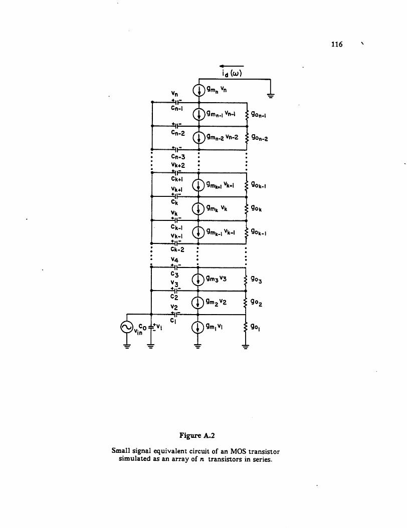
(~)v*o±:vi
Cn-I
Cn-2
-*IF-Cn-3
Vk*2
Ck+I
id (w)
pgmnvn
T)gmn.,vn-I |gon.i
T)gmn.2Vn-2 |gon.2
. QjWlVl | flowVk*l^FCk
Vk
Ck-I
Vk-I
Ck-2
ll CO8"**3C2
V2
C|
J)gmkvk |g0k
T)flmk.,vk-I |gok.,
r)gm2V2
g°3
go2
g0|
"'
Figure A.2
Small signal equivalent circuit of an MOS transistorsimulated as an array of n transistors in series.
116

117
single effective pole at the frequency
It can be shown that
thus
= 1P2*/fectivt "*" i=» j (A.2)tf fecuvt 1=00 1
*1 =i=eo
z1
1=0 A
^2«//«aiv»1
*1
(A.3)
(A.4)
&! can be found by using the Zero-Value Time Constant [16] method for which
i=0
and
To4 = *0jlC* (A.6)where R0 is the driving point resistance at the Ck node pair with all other capacitors
set to zero.
To find the driving point resistance of the kth capacitor nodes, all the other capa
citors are set to zero and a test current. ix. is applied to the corresponding nodes as
shown in Fig. A.3(a). The resulting vx is calculated as
Kt =f CA.7)In order to find this we need to know the output conductance and transconductance of
each transistor. These parameters are found to be equal to
«•«,! =8".,^^^ (A.5)
(A.9)&m(M. 1 &mar<M»)
Vn-*+l - y/n-k
C0XWL (A10)0 2n
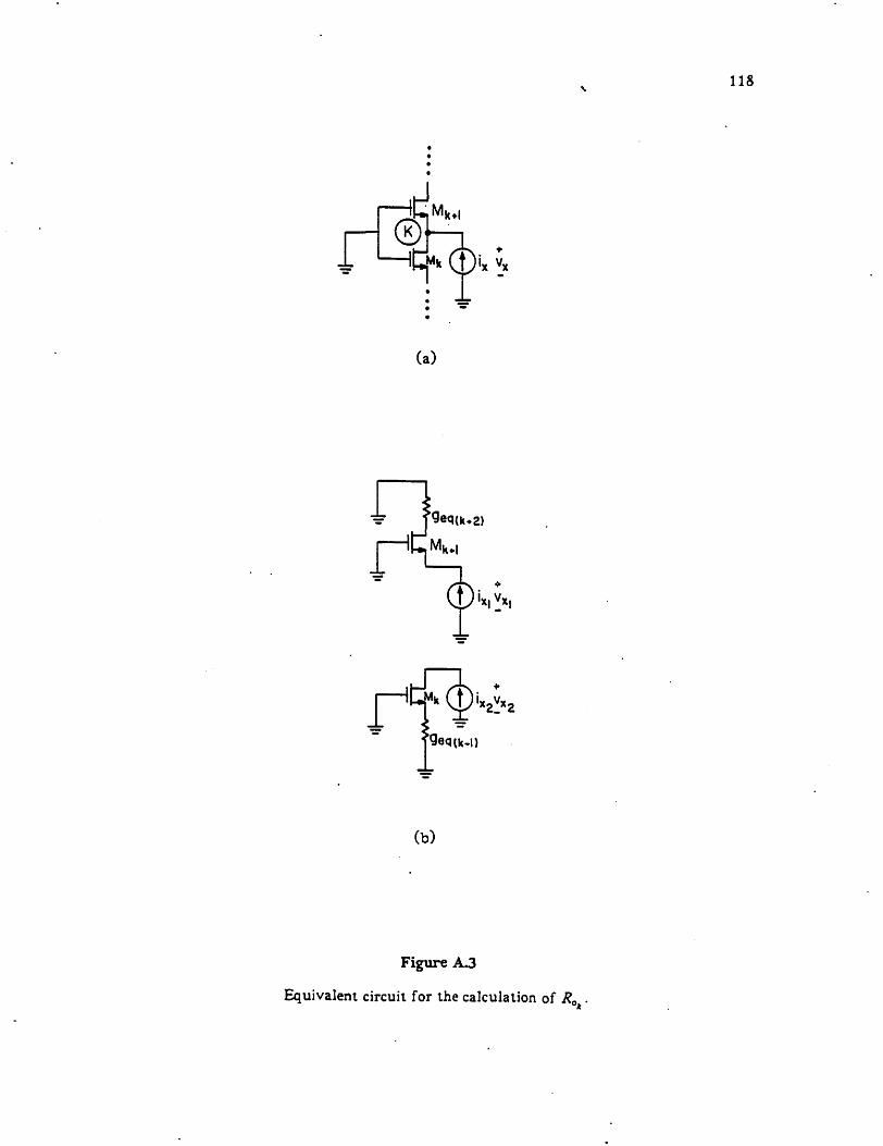
UMk*l
®lCjMk (pix {*
(a)
MM
OXvx,
(b)
Figure A3
Equivalent circuit for the calculation of RB
118

119
C\ - C2 - = c„.2=CoxWL
(A.ll)
C„ _i - -g— Cox WZ, (A.12)
where gmtKt , and g0/]Lf are the transconductance and output conductance of the klh
transistor. It is easier to break the connection at node k and find the contribution of
Mk+l and Mk separately. Fig. A.3(b) shows the equivalent circuit for the calculation
of R0jt. In this case
lxl lx2
ix l ix2Let's define as 2S„ and as eD%0 . thusvxl «"*♦, vx2 BD«k
&>* " *s~ . + to*
It can be found that
g5"*,i go^+i +g/X+iand
1 +aM
*-l
&?**;
S^m, &°Mk1 +
£«9*-l
note that g^., =g^ and g^ =g^
Substituting for (A.8) and (A.9) and manipulating the above equation
y/n
:t2
and
gsM^, *«»o Vn-jfc4*-i
gz\,A - g.Vn U -* )
'Aft °'"0 £
substituting from (A.17) and (A.18) in (A.14)
(A.13)
(A.14)
(A.15)
(A.16)
(A.17)
(A.18)

go* = gm0Jn Vn-*
Vn-*
or
go* gm° ky/n-k0<k <n-l
to find the Zero-VoZue Time Constant
i=n-l r»,- zfsubstituting from (A. 11) and (A. 12)
61 =C0XWL 'jr2 1 7CoxWL 1
6 n &*-»substituting from (A.20)
6,=Cft, WX
n2Vn" g,
*=n-2
S>v"-* +toWfor n -»00 the above series could be transformed to
*,=
or
but
Thus £ 1 is found to be
or
CoaWL
g"»o
r(i-) r(2)
6,=C^WX 4
**-« 15
C03tWX, =3_ j_gmfl 2 CD,
*,= 1 _L5 ctir
120
(A.19)
(A.20)
(A.21)
(A.22)
(A.23)
(A.24)
(A.25)
(A.26)
(A.27)
P2 ,,_ as2.5 <*>, (A.28)
This implies that the transconductance of an MOS transistor has a value lower by

121
—3dB at 2.5cor compared to it's DC value. Fig. A.4(a) gives the approximate location
of the poles and Fig. A.4(b) shows the location of the effective pole.
To verify this result an MOS transistor was simulated by the computer circuit
simulation program SPICE [21] by modeling the transistor as 36 transistors in series
which is a more accurate analysis than the above one-pole approximation. The result is
shown in Fig.A.5 which proves that the Zero-Value Time Constant method is a relatively
reasonable method to find the effective pole of the response for frequencies up to about
2 <ot of the MOS transistor.
A.2. High-Frequency Input Admittance of the MOS transistor
For low frequencies the input admittance of the MOS transistor is capacitive and
Y* =sX^C0XWL (A.29)At high-frequencies, the distributed capacitance and channel resistance results in some
more singularities in the input admittance.
Analyzing the small signal equivalent circuit shown in Fig. A.2. it can be shown
that the input admittance has the form [23]
i=oo
nu+f)
1=1 Pi
By inspection it can be shown that the poles are exactly at the same locations as the
transconductance poles and the zeros are located in between the poles. The first singu
larity is a pole as shown in Fig. A.6 . For frequencies lower than about tat of the
transistor, finding the exact locations of all the poles and zeros is not necessary and the
input admittance can be well approximated by
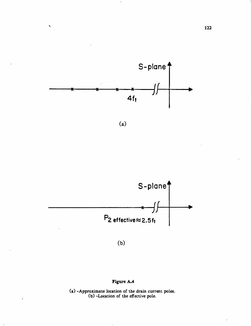
S-plane
•* *-
4ft#
(a)
S-planef
—If-^2effective« 2.5ft
(b)
Figure A.4
(a) -Approximate location of the drain current poles,(b) -Location of the effective pole.
122
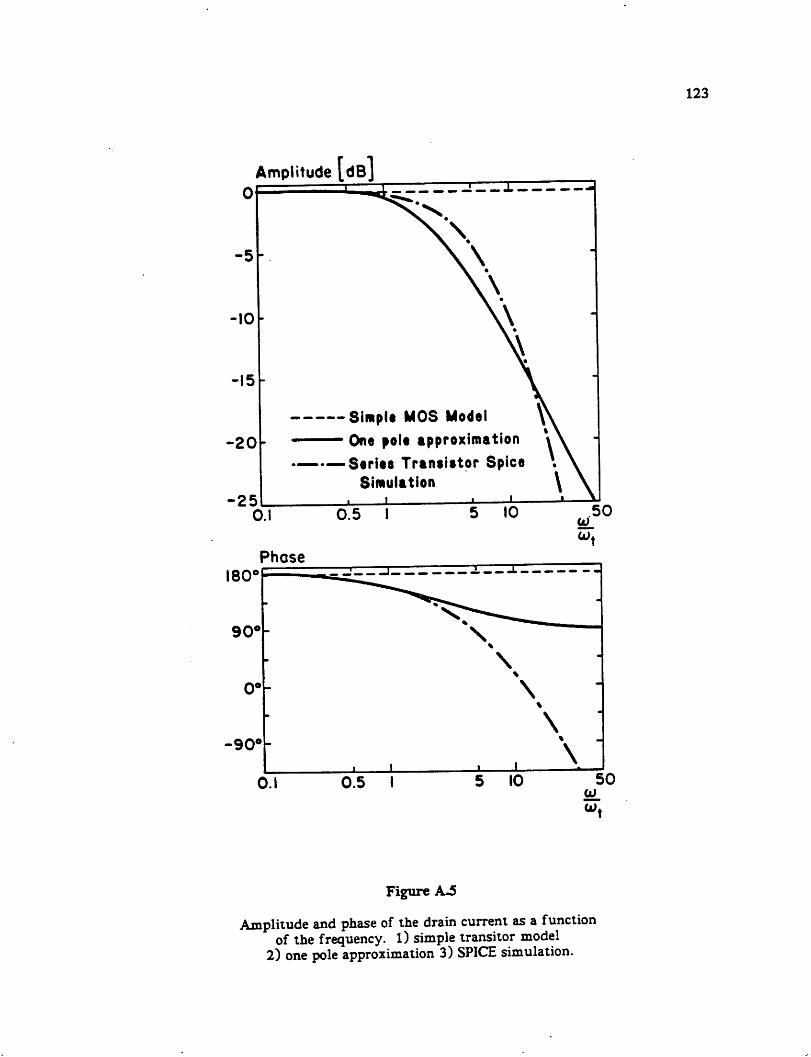
Amplitude
-5
-10
-15-
-20
-25
180
Simple MOS Model
—— On* pole approximation \
Series Transistor SpiceSimulation \
Figure A.5
Amplitude and phase of the drain current as a functionof the frequency. 1) simple transitor model
2) one pole approximation 3) SPICE simulation.
123
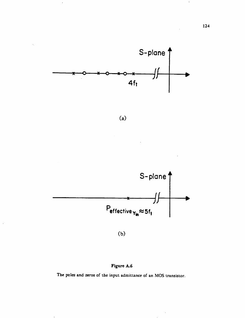
S-plane f
•*—O *—O K-O—*-
4ft
(a)
-If
S-plane
#effectivey. «5ft
(b)
Figure A.6
The poles and zeros of the input admittance of an MOS transistor.
124

125
i =00 1
(l+5£-L)ft/>i
It can be shown that y^ can be approximated as
* in *^^gj 1=00 1 1=00 1
ft /»i <ft *.•and
(A.32)
A//ecriv, * ^ ^ , (A 33)i =l />« i =1 2i
The easiest way to find peffeaivey is by SPICE simulation of a single transistor modeled
as many transistors in series which is shown in Fig. A.7. The 45 degree phase shift
point is found to be at about 5o>,. thus
Peffeaive ^ 5 Oit (A.34)As mentioned earlier the pole locations of Ym is exactly the same as the transconduc
tance. That is.
I — 88 T^~ <A'35),•=0 Pi 2.5 D(
from (A.33) (A.34) and (A.35). it can be concluded that
therefore
t=00 1 -I
Z — * ?f- (A.36)
1+ s
Y* * &« 5-T— (A*37)1 +
2.5 (d,
For all singularities represented by one effective pole.
Yin ^ sC
5 (D,

20Amplitude [dB]
Simple MOS Model
One pole approximation
—- — Series Transistor SpiceSimulation
"1
50
IPhase
90°i • i
45°
no i 1 i
0.1 0.5 10 50
Figure A.7
Amplitude and phase of the input admittance as afunction of frequency given by 1) simple transistor model
2) one pole approximation 3) SPICE simulation
126

127
In Fig. A.7 the result of the SPICE simulation of the input admitunce of an MOS
transistor is compared to the one-pole approximation.
The quality factor of the input capacitance is found to be
fit * £fL (A.39)Fig. A.8 shows an approximate equivalent circuit for the input admittance.
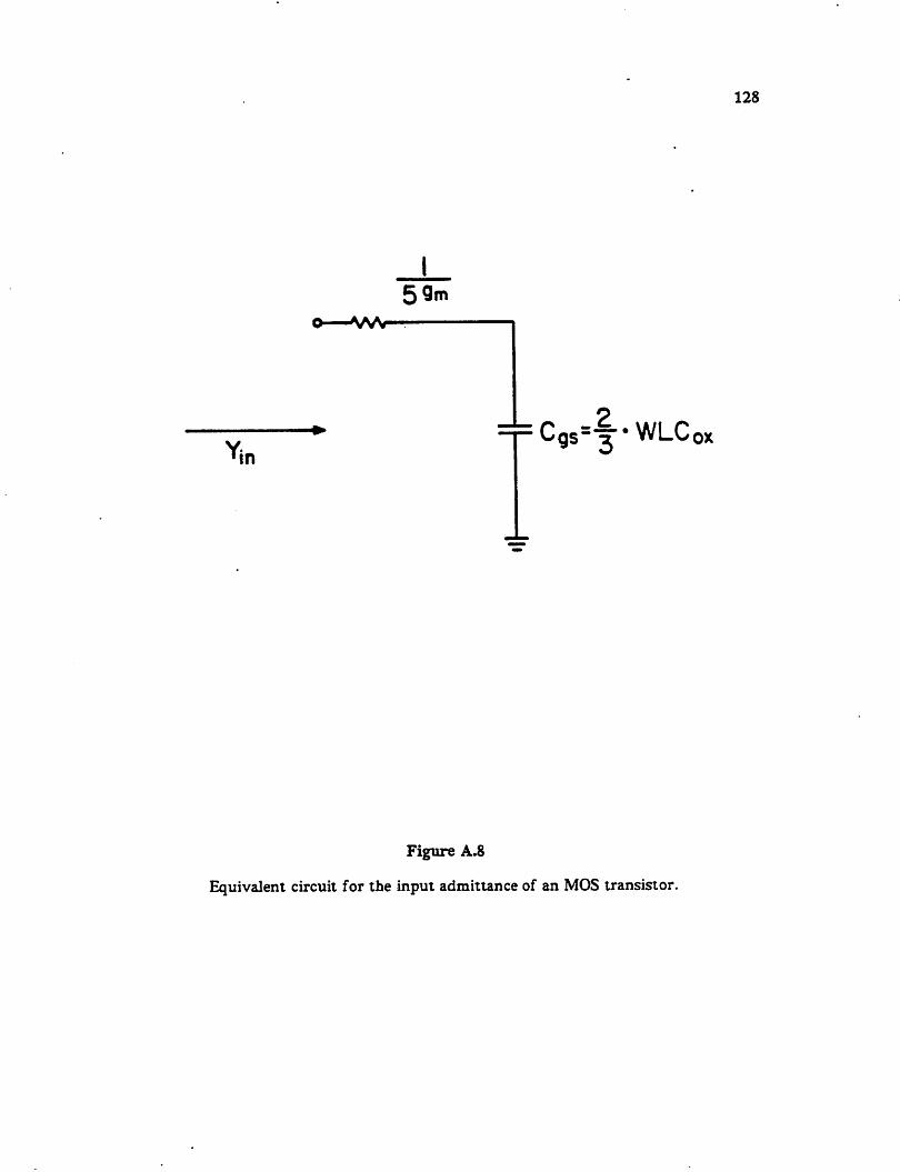
59mo vw
in
CgS=f'WLCox
Figure A.8
Equivalent circuit for the input admittance of an MOS transistor.
128

APPENDIX B
TOTAL OUTPUT NOISE POWER OF THE BANDPASS FILTER
To evaluate the filter noise performance, the total output noise power of a second
and sixth order bandpass filter is derived in this section.
For an nth order bandpass filter, made of n identical integrators, there exists n
independent noise sources. The total output noise power of the filter. vq\ . is given by
+00 +00
vT= J S. (/ )df ="f J ]ff„ (7/ )f S, (/ ) df (B.1)0 m-1 0
where
S0 (/ ) is the output noise spectral density.
Si (f ) is the input referred noise spectral density of an integrator.
Hm ()f ) is the transfer function of the mth node to the output of the filter.
The derivation of vqt could be drastically simplified by assuming that the input
referred noise spectral density of the integrator Si (f }m is frequency independent. In
chapter 4 it was shown that this assumption is indeed true for MOS integrators at high
frequencies. Thus the above equation simplifies to
vT=sittf "£./>,» u/)f«/ <B-2>m=l 0
To find the total output noise, the transfer function from each integrator input to the
output of the filter should be derived.
129
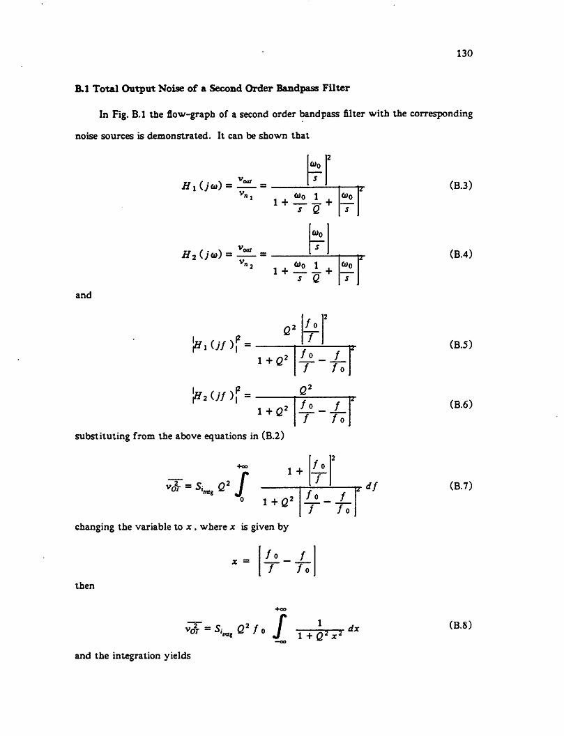
130
B.1 Total Output Noise of a Second Order Bandpass Filter
In Fig. B.l the flow-graph of a second order bandpass filter with the corresponding
noise sources is demonstrated. It can be shown that
v».
2(DO
S
a>o 1 , 0>01 + -7T +
s Q s
a>o
H2(jQ>) =
2 i + ^-U0)0
ir
and
PiO/)| =1 +Q4
1^2 (y/)!1-l + G2
substituting from the above equations in (B.2)
s Q
/o2
/
f /o
f /o
2+oo
1 +/o
/
XT
v* =S,mt Q: /0 1 + Q2
changing the variable to x . where x is given by
/ /o
x =
then
l±-±.f /o
v0r =S.Q2f0tmg
TOO
f _!J 1 + <3
and the integration yields
G7^<fx
df
(B.3)
(B.4)
(B.5)
(B.6)
(B.7)
(B.8)

Vin
-OUn/S
cu0/S
Figure B.1
The flow-graph of a second order bandpass filter withequivalent input referred integrator noise generators.
u>

132
vo2t=S> Q2f 0I * tan"1 Qx Ii +00
•«g Q lx =(B.9)
and finally
v02r =51|mgG fa* (B.IO)
B.2. Total Output Noise of a Sixth Order Bandpass Filter
The flow-graph of a sixth order bandpass filter, with the corresponding input
referred noise sources is shown in Fig. B.2. To find the transfer functions, the Mason's
theorem is used [24]
Hk (s) = Pk 4 (B.ll)
where A is the graph determinant. Pk is the direct path from node k to the output and
A* is the sum of those terms without any constituent loops touching Pk.
The denominator of all the transfer functions is equal to A and is found to be
Q s3+2/ +2 . 1
3
0>o
s
+2-
2
+ 2 '
o>0
s
2
4
4
<«>o
s
2
' Q
3
G>0
S
5
+o>0
s
Q
+
and the transfer functions are found to be
13«D0
H1 (jus) =
(D0
H2(jo>) =
y>(D0
H3(ju>) =
2
1 G>01 + JL _ +Q s
(Dq2\
(B.12)
(B.13)
(B.14)
(B.15)
Figure B.2
The flow-graph of a sixth order bandpass filter withequivalent input referred integrator noise generators.
H4(J<d) =
Hs(jo>) =
Hb(ju>) =
(Do
S
3
1 <«>0i + 4- — +
2 ^
0>o2
v A
Vour
V»5
(D0
S1+1 W° +[2 +̂ ) o>0
s
2(D0
S
3
+(D0
S
4
"out
V„
(D0
S
to0 to0
s
to0
using the derived transfer functions, it can be shown that
m=6
or
m=l
G2 iI +/o
/ J
2
1 + Q2/c
/
» __ // 0
X-
Ll-1.f /o
— ^2
/" /o + y
/ /o4-4y2
/ /o
+ 2y
+ 4 y4
134
(B.16)
(B.17)
(B.18)
(B.19)

m=6
Zm=lZ !*.(;/)"-
G2 l +/o
/ |
2
«• +
3y2G2 l +/of/ 1
l + G2ft
f
• // 0
r ~
l+<22/o
/. /
/o
2
Z±-J_/ /o "•-J
135
(B.20)
/ /o G'-Ay2
f /o+ 4/
Integrating both sides over the frequency range
+oo
/m=6 I I?
+00
/G2 1l +
/o2
l + G2 /c
./
> _ // 0
2
+oo
df + /v2G2 l +
/o
/ 1
2
l +G2/o
/_ /
/ 0
J
/ /o2v2-
Q'
/ /o-Ay2
f /o
12-
+ 4y
(B.21)
*/
Note that the first term on the right side is exactly the same as the equation found for
the second order filter, analyzed in the previous section, and is equal to
find the second term let's assume
G to" To
B =y2Q2f1 +
1 +G:
f_f |
/ /o
136
121
(B.22)
/ /o2v2-
/ /oi-4*
/ /o
df
+ 4 v4
changing the variable according to the following equation
then
+oo
- ».2* =Vz/o / x2+ !
x = ll-JLf /o
3x2-7 Q'
Q2" *' + G-4v2 x2 + 4 y4
The above equation can be transformed to the form
B = /oQ27^ "•-i
+0O
/
changing variable
G2Ay4 r G
3x
2^-
r- 1.2 1
2y2
rfx (B.23)
(B.24)
dx
- 1 + 1
Then
or
yields to
u = 2y2--L2y2-
-1
+00
B ~f°~L Q2u*+1 du
.2 I 1+00
B = f aQ— IJ- tan"1 G " I70 2 |G * |.„
137
(B.25)
(B.26)
7T5=/0Qy (B.27)
Adding the above value to the value found from the integration of the first term from
equation (B.21)
f z i»»o/>jV =/„e If-% m=l *•
and substituting in equation (B.2)
3ttv02r=5lnBg/oG 2
(B.28)
(B.29)
REFERENCES
[l] K.S. Tan. P.R. Gray. "Fully integrated analog filters using bipolar-JFET technol
ogy." IEEE Journal of Solid-State Circuits . Vol. SC-13 No.6. pp. 814-821.
December 1978.
[2] M. Banu. Y. Tsividis. "Fully integrated active RC filters in MOS technology."
IEEE Journal of Solid-State Circuits . Vol. SC-18 No.6. pp. 644-651. December
1983.
[3] T.C. Choi. R.T. Kaneshiro. R.W. Brodersen. P.R. Gray. W.B. Jett. M. Wilcox.
"High-frequency CMOS switched-capacitor filters for communication applica
tions." IEEE Journal of Solid-State Circuits . Vol. SC-18 No.6. pp. 652-664.
December 1983.
[4] S. Masuda. Y. Kitamura. S. Ohya. M. Kikuchi. "CMOS sampled differential
push-pull cascode operational amplifier." Proc. IEEE Int. Symp. Circuits Syst., pp.
1211-1214. May 1984.
[5] K.W. Moulding. J.R. Quartly. P.J. Rankin. R.S. Thompson. G.A. Wilson. "Gyratpr
video filter IC with automatic tuning." IEEE Journal of Solid-State Circuits . Vol.
SC-15 No.6. pp. 963-968. December 1980. "CMOS sampled differential push-pull
cascode operational amplifier." Proc. IEEE Int. Symp. Circuits Syst., May 1984.
pp. 1211-1214.
[6] P.O. Brackett and A.S. Sedra "Active compensation for high frequency effects in
op amp circuits with applications to active RC filters." IEEE Trans. Circuits and
Systems, Vol. CAS-23. pp. 68-72. February 1976.
[7] H.J. Orchard. "Inductorless filters." Electron. Lett., Vol. 2. pp. 224-225. Sep
tember 1966.
138

139
[8] K.R. Laker. M.S. Ghausi and J.J. Kelly. "Minimum sensitivity active and passive
ladder bandpass filters." IEEE Trans. Circuits and Systems, Vol. CAS-22. pp.
670-677. August 1975.
[9] W.E. Heinlein and W.H. Holmes, Active Filters for Integrated Circuits,
Prentice-Hall International. Inc. Chapter 8. 1974.
[10] A. I. Zverev. Handbook of Filter Synthesis, New York: Wiley. 1967.
[ll] L.T. Bruton, "Multiple-amplifier RC-active filter design with emphasis on GIC
realizations." IEEE Trans. Circuits and Systems, Vol. CAS-25. pp. 830-845
October 1978.
[12] G. Szentirmai. "FILSYN- a general purpose filter synthesis program." Proc. IEEE,
Vol. 65. pp. 1443.1458. October 1977.
[13] R.G. Meyer. "Nonlinear analog integrated circuits." EECS 240 class notes. Univer
sity of California. Berkeley. 1976.
[14] T.C. Choi. "High frequency CMOS switched-capacitor filters." Ph.D. Thesis. ERL
Memo No. UCB/ERL M83/31. Electronics Research Laboratory. University of
California. Berkeley. CA.. May 1983.
[15] K.C. Hsieh. "Noise limitations in switched-capacitor filters." Ph.D. Thesis. ERL
Memo No. UCB/ERL M82/39. Electronics Research Laboratory. University of
California. Berkeley. CA.. May 1983.
[16] P.R. Gray. R.G. Meyer. Analysis and Design of Analog Integrated Circuits. New
York: Wiley. 1984.
[17] F. M. Gardner. Phaselock Techniques, New York: Wiley. 1979.
[18] A. Blanchard. Phase-Locked Loops : Applications to Coherent Receiver Design.
New York: Wiley. 1976.

140
[19] M.U. Bartz. "A direct-coupled MOS Analog multiplier." M.Sc. Report. Electronics
Research Laboratory. University of California. Berkeley. CA.. June 1980.
[20] H. Khorramabadi. "NMOS Phase-locked loop." M.Sc. Report. ERL Memo No.
UCB/ERL M77/67. Electronics Research Laboratory. University of California.
Berkeley. CA.. November 1977.
[21] L.W. Nagel. "SPICE2- a computer program to simulate semiconductor circuits."
Electronics Research Laboratory. ERL Memo No. UCB/ERL M520. University of
California. Berkeley. CA.. May 1975.
[22] J.R. Burns. "High frequency characteristics of the Insulated Gate Field Effect
transistor." RCA Review. Vol. 28. pp. 385 September 1967.
[23] M.S. Ghausi. J.J. Kelly. Introduction to Distributed Parameter Networks: with an
Application to Integrated Circuits, New York: Holt. Rinehart and Winston. Inc..
1968.
[24] S.J. Mason. H.J. Zimmermann. Electronics Circuits, Signals and Systems. New
York: Wiley. 1960.


![INDEX.* [digitalassets.lib.berkeley.edu]digitalassets.lib.berkeley.edu/anthpubs/ucb/text/ucp006...Buckingham's island, 206. Bucknell ranch, 188. Buckner creek, 143, 259; moun-tains,](https://img.pdfslide.us/doc/110x75/5afedb927f8b9a864d8f89bb/index-s-island-206-bucknell-ranch-188-buckner-creek-143-259-moun-tains.jpg)


![INDEX.* [digitalassets.lib.berkeley.edu]digitalassets.lib.berkeley.edu/anthpubs/ucb/text/ucp008-009.pdf · Keruk, 277, 283, 294, 311, 336, 337, 358. Kimul Chehenish, 103. Kish, 102,](https://img.pdfslide.us/doc/110x75/5cc16c2188c99315158c0e6a/index-keruk-277-283-294-311-336-337-358-kimul-chehenish-103.jpg)