Embed Size (px)
Citation preview
Copper Halide Semiconductors for Room Temperature Quantum
Applications – A Materials Perspective
R.K. Vijayaraghavan, S. Daniels and P. McNally
School of Electronic Engineering, Dublin City University

Acknowledgements
• DCU: Aidan Cowley, Barry Foy, Francis Olabanji Lucas, Lisa O’Reilly, Prof. Enda McGlynn, Prof. Martin Henry.
• TCD: Anirban Mitra, Daniel Danieluk, Prof. Louise Bradley (TCD).
2
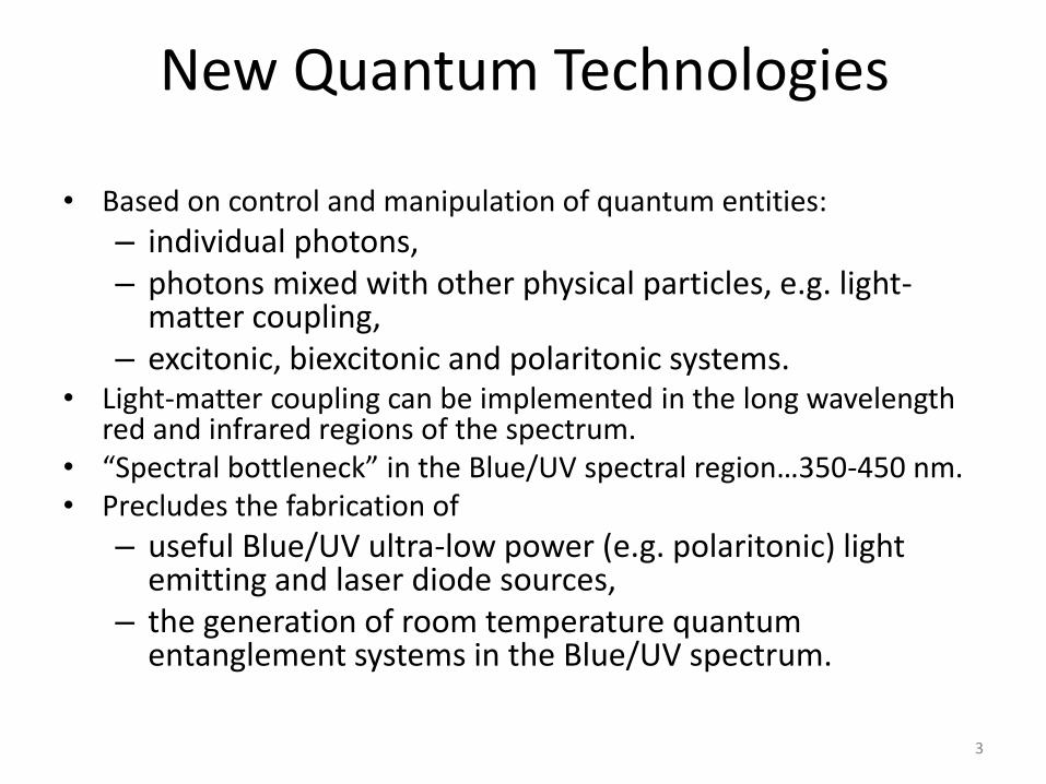
New Quantum Technologies
• Based on control and manipulation of quantum entities:
– individual photons, – photons mixed with other physical particles, e.g. light-
matter coupling, – excitonic, biexcitonic and polaritonic systems.
• Light-matter coupling can be implemented in the long wavelength red and infrared regions of the spectrum.
• “Spectral bottleneck” in the Blue/UV spectral region…350-450 nm. • Precludes the fabrication of
– useful Blue/UV ultra-low power (e.g. polaritonic) light emitting and laser diode sources,
– the generation of room temperature quantum entanglement systems in the Blue/UV spectrum.
3
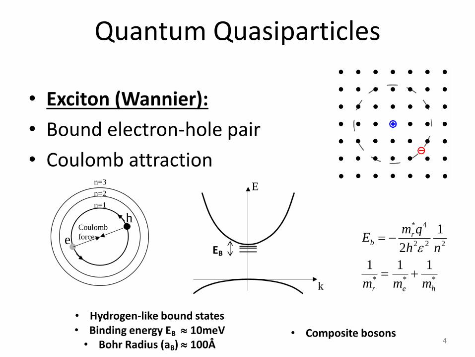
Quantum Quasiparticles
• Exciton (Wannier):
• Bound electron-hole pair
• Coulomb attraction
• Hydrogen-like bound states • Binding energy EB 10meV • Bohr Radius (aB) 100Å
e
hCoulomb
force
n=3
n=2
n=1
E
k
EbEB
***
222
4*
111
1
2
her
rb
mmm
nh
qmE
• Composite bosons 4
Quantum Quasiparticles
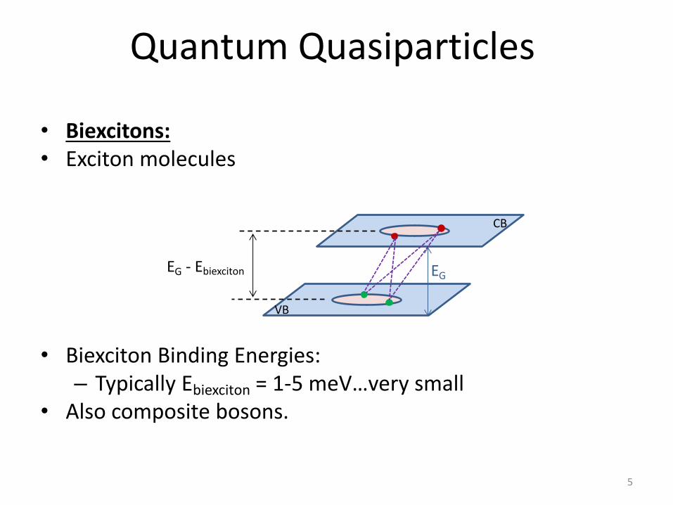
• Biexcitons: • Exciton molecules
• Biexciton Binding Energies: – Typically Ebiexciton = 1-5 meV…very small
• Also composite bosons.
EG - Ebiexciton EG
CB
VB
5
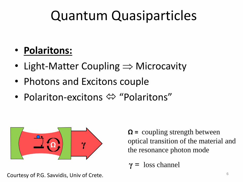
Quantum Quasiparticles
• Polaritons:
• Light-Matter Coupling Microcavity
• Photons and Excitons couple
• Polariton-excitons “Polaritons”
γ = loss channel
Ω = coupling strength between
optical transition of the material and
the resonance photon mode γ Ω
Courtesy of P.G. Savvidis, Univ of Crete. 6
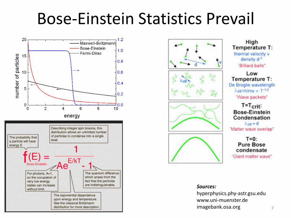
Bose-Einstein Statistics Prevail
Sources: hyperphysics.phy-astr.gsu.edu www.uni-muenster.de imagebank.osa.org 7
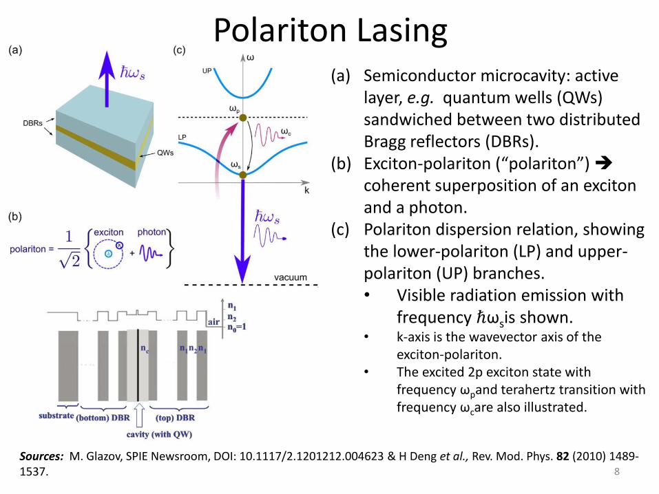
Polariton Lasing (a) Semiconductor microcavity: active
layer, e.g. quantum wells (QWs) sandwiched between two distributed Bragg reflectors (DBRs).
(b) Exciton-polariton (“polariton”) coherent superposition of an exciton and a photon.
(c) Polariton dispersion relation, showing the lower-polariton (LP) and upper-polariton (UP) branches. • Visible radiation emission with
frequency ℏωsis shown. • k-axis is the wavevector axis of the
exciton-polariton. • The excited 2p exciton state with
frequency ωpand terahertz transition with frequency ωcare also illustrated.
Sources: M. Glazov, SPIE Newsroom, DOI: 10.1117/2.1201212.004623 & H Deng et al., Rev. Mod. Phys. 82 (2010) 1489-1537.
8
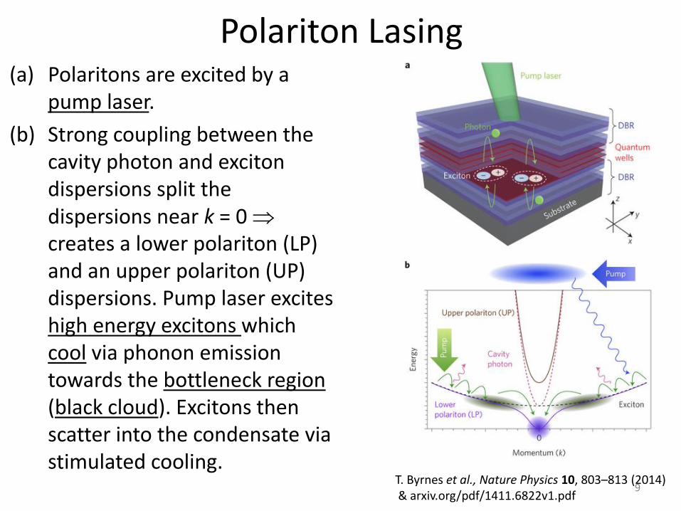
T. Byrnes et al., Nature Physics 10, 803–813 (2014) & arxiv.org/pdf/1411.6822v1.pdf
(a) Polaritons are excited by a pump laser.
(b) Strong coupling between the cavity photon and exciton dispersions split the dispersions near k = 0 creates a lower polariton (LP) and an upper polariton (UP) dispersions. Pump laser excites high energy excitons which cool via phonon emission towards the bottleneck region (black cloud). Excitons then scatter into the condensate via stimulated cooling.
Polariton Lasing
9
Polaritonic Light Emitters
• Polaritons behave like electrons/holes with an effective mass 1/10,000 that of an electron!
• Different lasing mechanism possible “polaritonic lasing”.
• Lasing threshold current densities 2-3 orders of magnitude lower than for conventional laser diodes (LDs).
• Conventional LD: Jth = 10,000 Acm-2
• Polaritonic LD: Jth = 100 Acm-2
• Ultra efficient; ultra low power light emission possible.
10
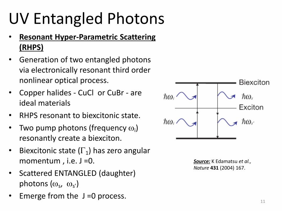
UV Entangled Photons • Resonant Hyper-Parametric Scattering
(RHPS)
• Generation of two entangled photons via electronically resonant third order nonlinear optical process.
• Copper halides - CuCl or CuBr - are ideal materials
• RHPS resonant to biexcitonic state.
• Two pump photons (frequency wi) resonantly create a biexciton.
• Biexcitonic state (G1) has zero angular momentum , i.e. J =0.
• Scattered ENTANGLED (daughter) photons (ws, ws’)
• Emerge from the J =0 process.
Source: K Edamatsu et al., Nature 431 (2004) 167.
11
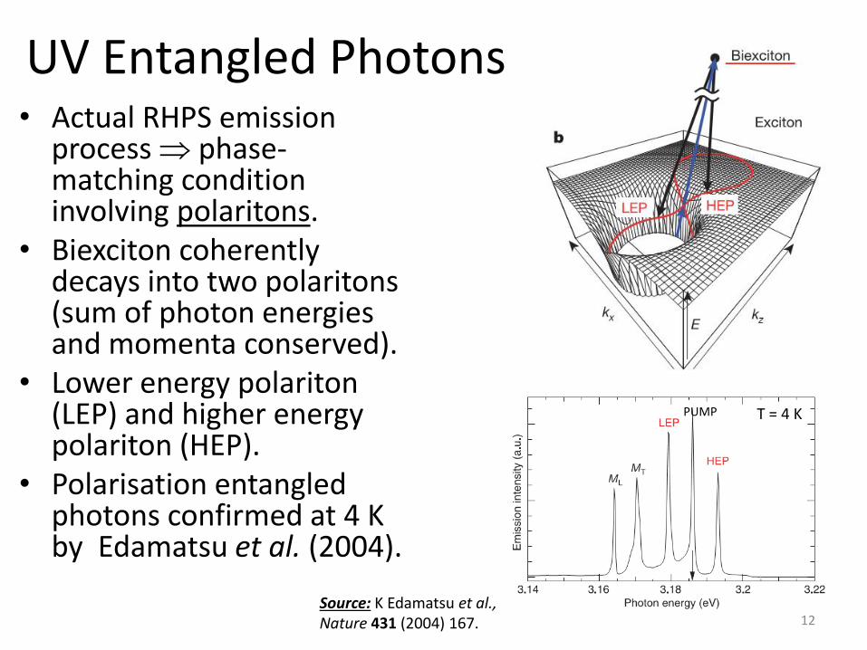
PUMP T = 4 K
• Actual RHPS emission process phase-matching condition involving polaritons.
• Biexciton coherently decays into two polaritons (sum of photon energies and momenta conserved).
• Lower energy polariton (LEP) and higher energy polariton (HEP).
• Polarisation entangled photons confirmed at 4 K by Edamatsu et al. (2004).
UV Entangled Photons
Source: K Edamatsu et al., Nature 431 (2004) 167. 12
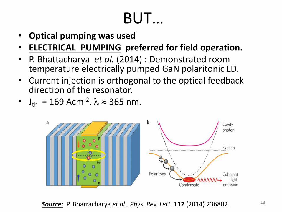
BUT… • Optical pumping was used • ELECTRICAL PUMPING preferred for field operation. • P. Bhattacharya et al. (2014) : Demonstrated room
temperature electrically pumped GaN polaritonic LD. • Current injection is orthogonal to the optical feedback
direction of the resonator. • Jth = 169 Acm-2. l 365 nm.
Source: P. Bharracharya et al., Phys. Rev. Lett. 112 (2014) 236802. 13
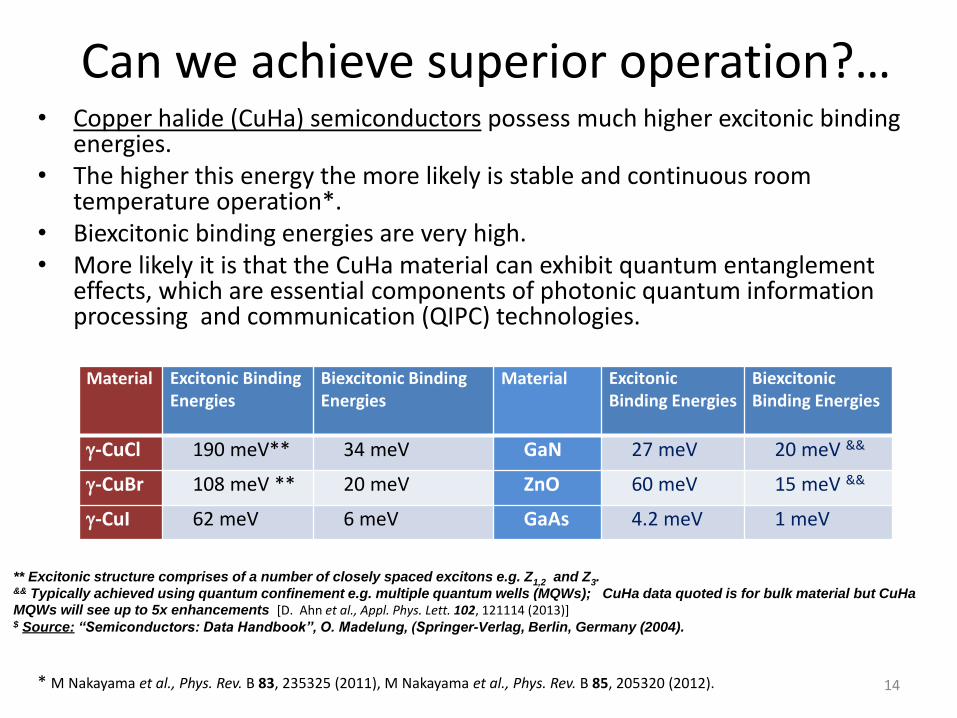
Can we achieve superior operation?… • Copper halide (CuHa) semiconductors possess much higher excitonic binding
energies. • The higher this energy the more likely is stable and continuous room
temperature operation*. • Biexcitonic binding energies are very high. • More likely it is that the CuHa material can exhibit quantum entanglement
effects, which are essential components of photonic quantum information processing and communication (QIPC) technologies.
* M Nakayama et al., Phys. Rev. B 83, 235325 (2011), M Nakayama et al., Phys. Rev. B 85, 205320 (2012).
Material Excitonic Binding Energies
Biexcitonic Binding Energies
Material Excitonic Binding Energies
Biexcitonic Binding Energies
g-CuCl 190 meV** 34 meV GaN 27 meV 20 meV &&
g-CuBr 108 meV ** 20 meV ZnO 60 meV 15 meV &&
g-CuI 62 meV 6 meV GaAs 4.2 meV 1 meV
** Excitonic structure comprises of a number of closely spaced excitons e.g. Z1,2 and Z3. && Typically achieved using quantum confinement e.g. multiple quantum wells (MQWs); CuHa data quoted is for bulk material but CuHa MQWs will see up to 5x enhancements [D. Ahn et al., Appl. Phys. Lett. 102, 121114 (2013)]
$ Source: “Semiconductors: Data Handbook”, O. Madelung, (Springer-Verlag, Berlin, Germany (2004).
14
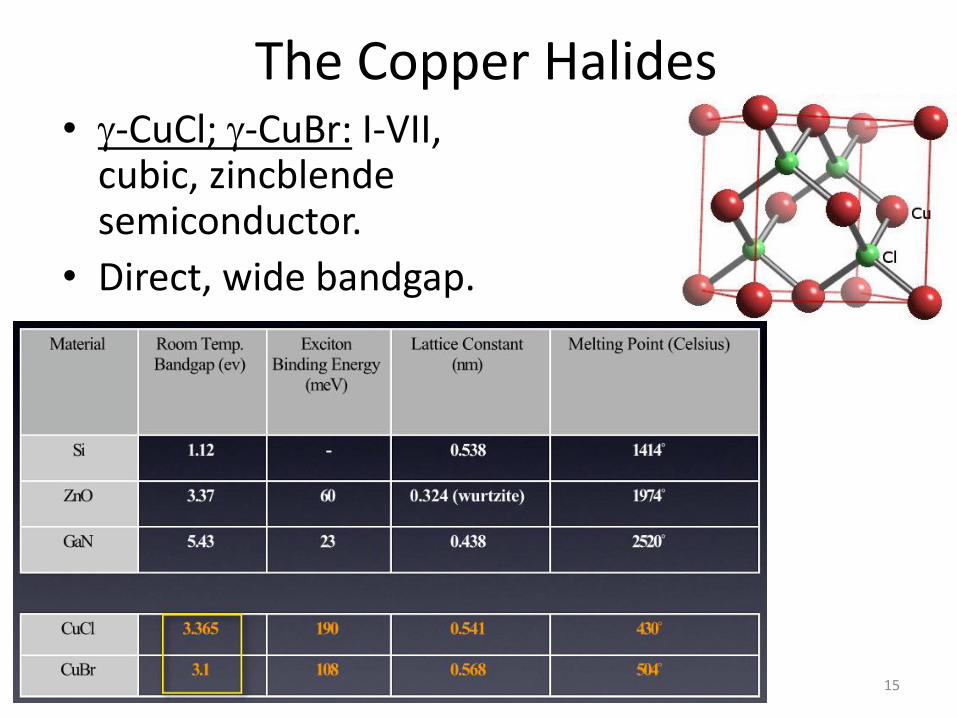
The Copper Halides • g-CuCl; g-CuBr: I-VII,
cubic, zincblende semiconductor.
• Direct, wide bandgap.
15
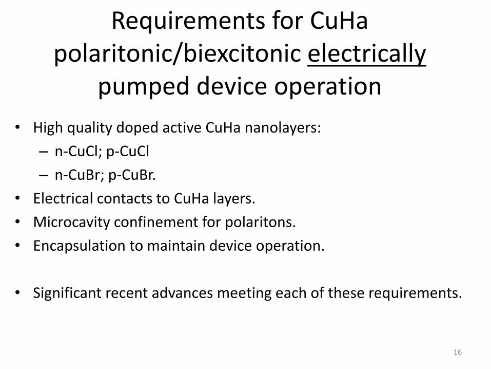
Requirements for CuHa polaritonic/biexcitonic electrically
pumped device operation
• High quality doped active CuHa nanolayers:
– n-CuCl; p-CuCl
– n-CuBr; p-CuBr.
• Electrical contacts to CuHa layers.
• Microcavity confinement for polaritons.
• Encapsulation to maintain device operation.
• Significant recent advances meeting each of these requirements.
16
Cl
Cu
Zn
e-
Cu vacancy
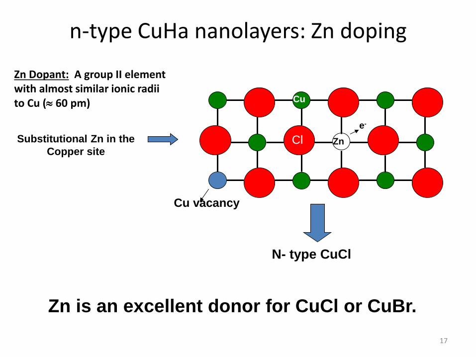
n-type CuHa nanolayers: Zn doping
Substitutional Zn in the
Copper site
N- type CuCl
Zn is an excellent donor for CuCl or CuBr.
Zn Dopant: A group II element with almost similar ionic radii to Cu ( 60 pm)
17
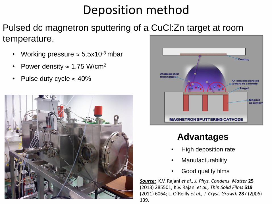
Deposition method
• Working pressure 5.5x10⁻³ mbar
• Power density 1.75 W/cm2
• Pulse duty cycle 40%
Pulsed dc magnetron sputtering of a CuCl:Zn target at room
temperature.
Advantages
• High deposition rate
• Manufacturability
• Good quality films
Source: K.V. Rajani et al., J. Phys. Condens. Matter 25 (2013) 285501; K.V. Rajani et al., Thin Solid Films 519 (2011) 6064; L. O’Reilly et al., J. Cryst. Growth 287 (2006) 139.
18
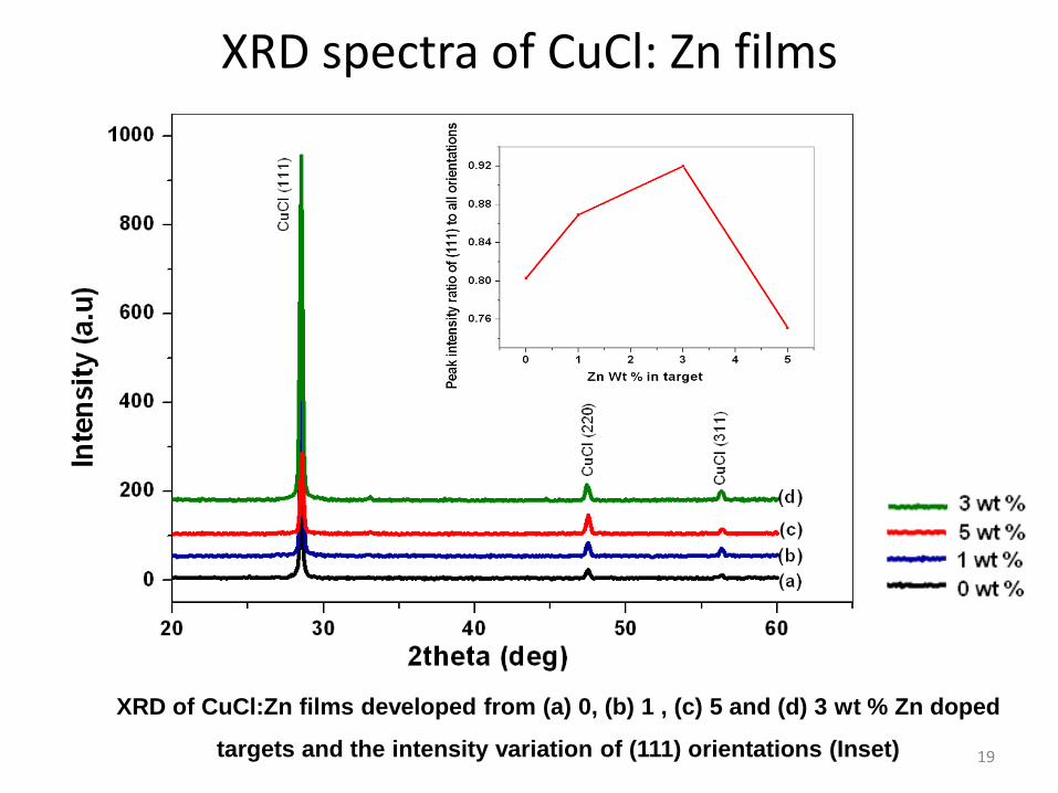
XRD spectra of CuCl: Zn films
XRD of CuCl:Zn films developed from (a) 0, (b) 1 , (c) 5 and (d) 3 wt % Zn doped
targets and the intensity variation of (111) orientations (Inset)
19
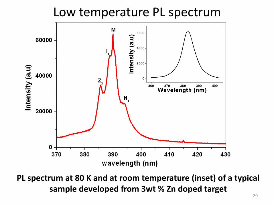
Low temperature PL spectrum
PL spectrum at 80 K and at room temperature (inset) of a typical sample developed from 3wt % Zn doped target
20
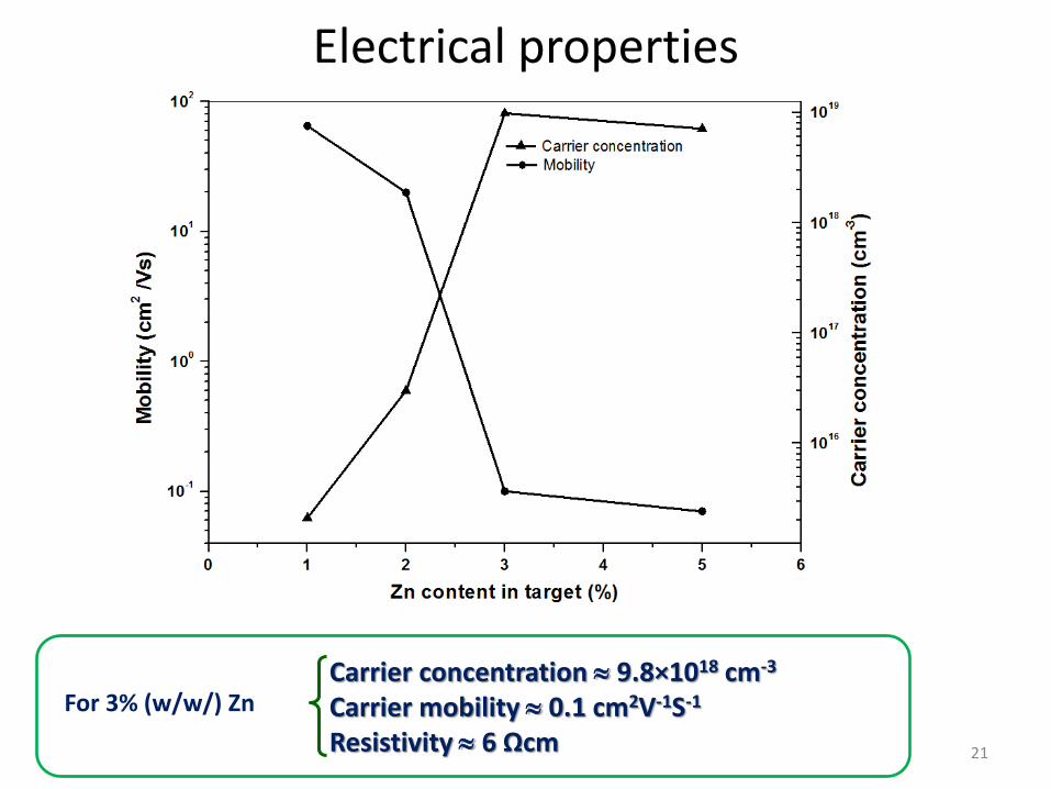
Electrical properties
Carrier concentration 9.8×1018 cm-3 Carrier mobility 0.1 cm2V-1S-1
Resistivity 6 Ωcm
For 3% (w/w/) Zn
21
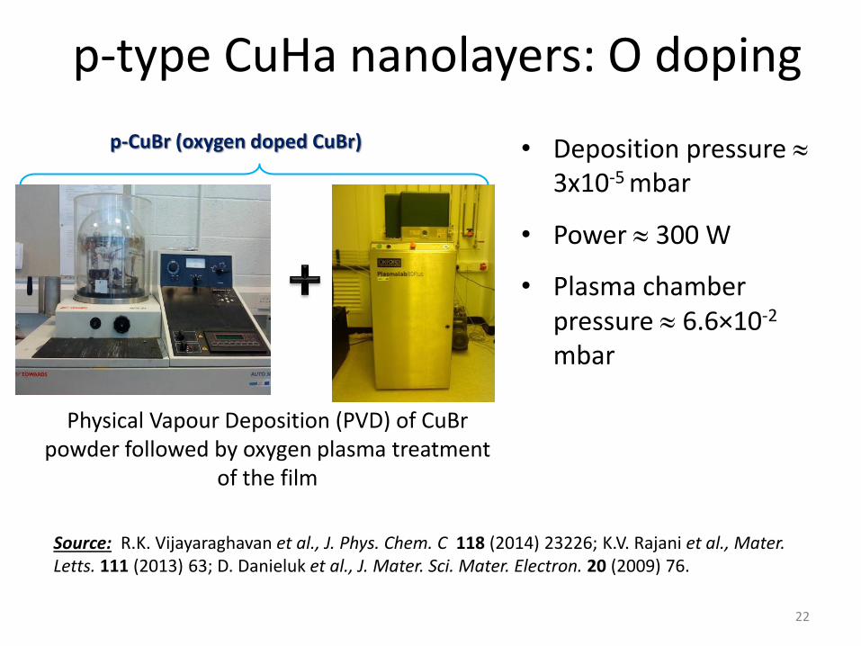
p-type CuHa nanolayers: O doping
• Deposition pressure 3x10⁻⁵ mbar
• Power 300 W
• Plasma chamber pressure 6.6×10⁻² mbar
Source: R.K. Vijayaraghavan et al., J. Phys. Chem. C 118 (2014) 23226; K.V. Rajani et al., Mater. Letts. 111 (2013) 63; D. Danieluk et al., J. Mater. Sci. Mater. Electron. 20 (2009) 76.
p-CuBr (oxygen doped CuBr)
Physical Vapour Deposition (PVD) of CuBr powder followed by oxygen plasma treatment
of the film
22
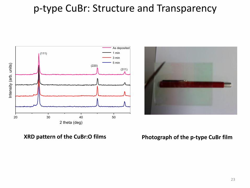
p-type CuBr: Structure and Transparency
20 30 40 50
As deposited
1 min
3 min
5 min
Inte
nsity (
arb
. u
nits)
2 theta (deg)
(111)
(220)
(311)
XRD pattern of the CuBr:O films Photograph of the p-type CuBr film
23
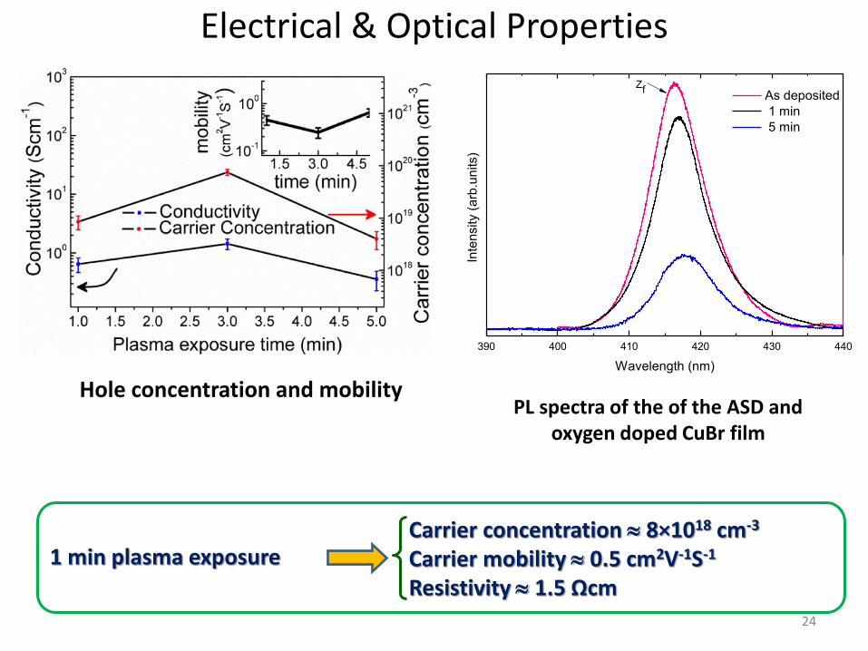
Electrical & Optical Properties
Hole concentration and mobility
1 min plasma exposure Carrier concentration 8×1018 cm-3 Carrier mobility 0.5 cm2V-1S-1
Resistivity 1.5 Ωcm
390 400 410 420 430 440
As deposited
1 min
5 min
Inte
nsity (
arb
.un
its)
Wavelength (nm)
Zf
PL spectra of the of the ASD and oxygen doped CuBr film
24
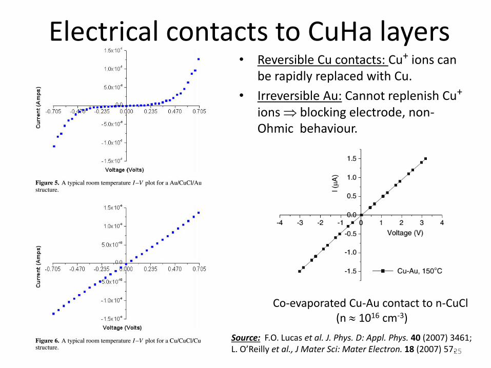
Electrical contacts to CuHa layers • Reversible Cu contacts: Cu+ ions can
be rapidly replaced with Cu.
• Irreversible Au: Cannot replenish Cu+ ions blocking electrode, non-Ohmic behaviour.
Source: F.O. Lucas et al. J. Phys. D: Appl. Phys. 40 (2007) 3461; L. O’Reilly et al., J Mater Sci: Mater Electron. 18 (2007) 57.
Co-evaporated Cu-Au contact to n-CuCl (n 1016 cm-3)
25
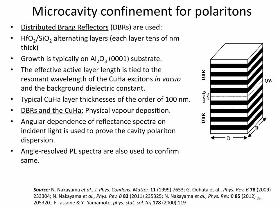
Microcavity confinement for polaritons • Distributed Bragg Reflectors (DBRs) are used:
• HfO2/SiO2 alternating layers (each layer tens of nm thick)
• Growth is typically on Al2O3 (0001) substrate.
• The effective active layer length is tied to the resonant wavelength of the CuHa excitons in vacuo and the background dielectric constant.
• Typical CuHa layer thicknesses of the order of 100 nm.
• DBRs and the CuHa: Physical vapour deposition.
• Angular dependence of reflectance spectra on incident light is used to prove the cavity polariton dispersion.
• Angle-resolved PL spectra are also used to confirm same.
Source: N. Nakayama et al., J. Phys. Condens. Matter. 11 (1999) 7653; G. Oohata et al., Phys. Rev. B 78 (2009) 233304; N. Nakayama et al., Phys. Rev. B 83 (2011) 235325; N. Nakayama et al., Phys. Rev. B 85 (2012) 205320.; F Tassone & Y. Yamamoto, phys. stat. sol. (a) 178 (2000) 119 .
26
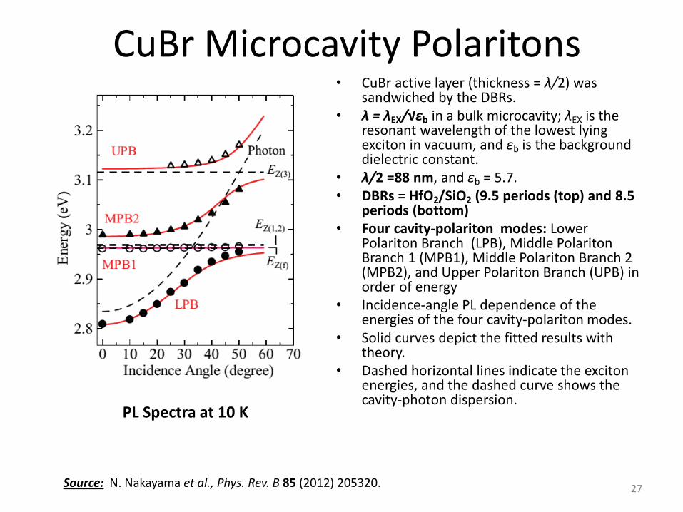
CuBr Microcavity Polaritons • CuBr active layer (thickness = λ/2) was
sandwiched by the DBRs. • λ = λEX/√εb in a bulk microcavity; λEX is the
resonant wavelength of the lowest lying exciton in vacuum, and εb is the background dielectric constant.
• λ/2 =88 nm, and εb = 5.7. • DBRs = HfO2/SiO2 (9.5 periods (top) and 8.5
periods (bottom) • Four cavity-polariton modes: Lower
Polariton Branch (LPB), Middle Polariton Branch 1 (MPB1), Middle Polariton Branch 2 (MPB2), and Upper Polariton Branch (UPB) in order of energy
• Incidence-angle PL dependence of the energies of the four cavity-polariton modes.
• Solid curves depict the fitted results with theory.
• Dashed horizontal lines indicate the exciton energies, and the dashed curve shows the cavity-photon dispersion.
Source: N. Nakayama et al., Phys. Rev. B 85 (2012) 205320.
PL Spectra at 10 K
27
28
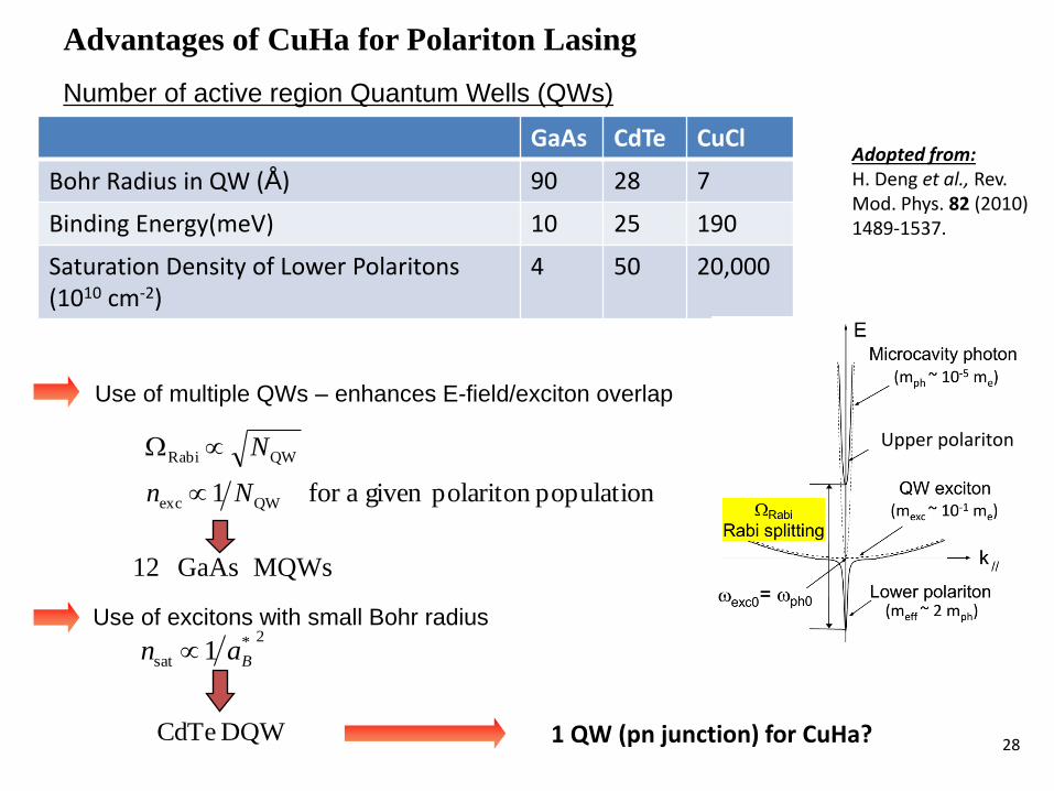
Number of active region Quantum Wells (QWs)
Use of multiple QWs – enhances E-field/exciton overlap
Use of excitons with small Bohr radius
populationpolaritongivenafor1 QWexc
QWRabi
Nn
N
MQWsGaAs12
2*
sat 1 Ban
DQWCdTe
Comparison of Exciton Properties
Advantages of CuHa for Polariton Lasing
GaAs CdTe CuCl
Bohr Radius in QW (Å) 90 28 7
Binding Energy(meV) 10 25 190
Saturation Density of Lower Polaritons (1010 cm-2)
4 50 20,000
1 QW (pn junction) for CuHa?
Adopted from: H. Deng et al., Rev. Mod. Phys. 82 (2010) 1489-1537.
Upper polariton
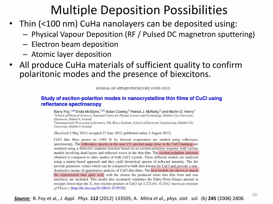
Multiple Deposition Possibilities • Thin (<100 nm) CuHa nanolayers can be deposited using:
– Physical Vapour Deposition (RF / Pulsed DC magnetron sputtering) – Electron beam deposition – Atomic layer deposition
• All produce CuHa materials of sufficient quality to confirm polaritonic modes and the presence of biexcitons.
Source: B. Foy et al., J. Appl. Phys. 112 (2012) 133505; A. Mitra et al., phys. stat. sol. (b) 245 (2008) 2808. 29
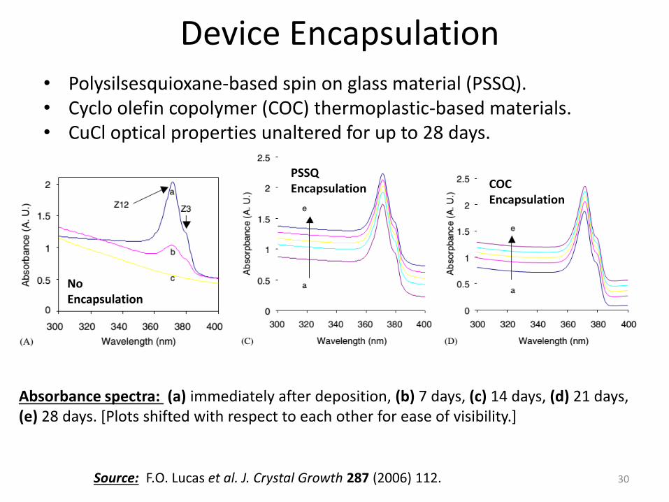
Device Encapsulation • Polysilsesquioxane-based spin on glass material (PSSQ). • Cyclo olefin copolymer (COC) thermoplastic-based materials. • CuCl optical properties unaltered for up to 28 days.
Source: F.O. Lucas et al. J. Crystal Growth 287 (2006) 112.
Absorbance spectra: (a) immediately after deposition, (b) 7 days, (c) 14 days, (d) 21 days, (e) 28 days. [Plots shifted with respect to each other for ease of visibility.]
30
PSSQ Encapsulation COC
Encapsulation
No Encapsulation
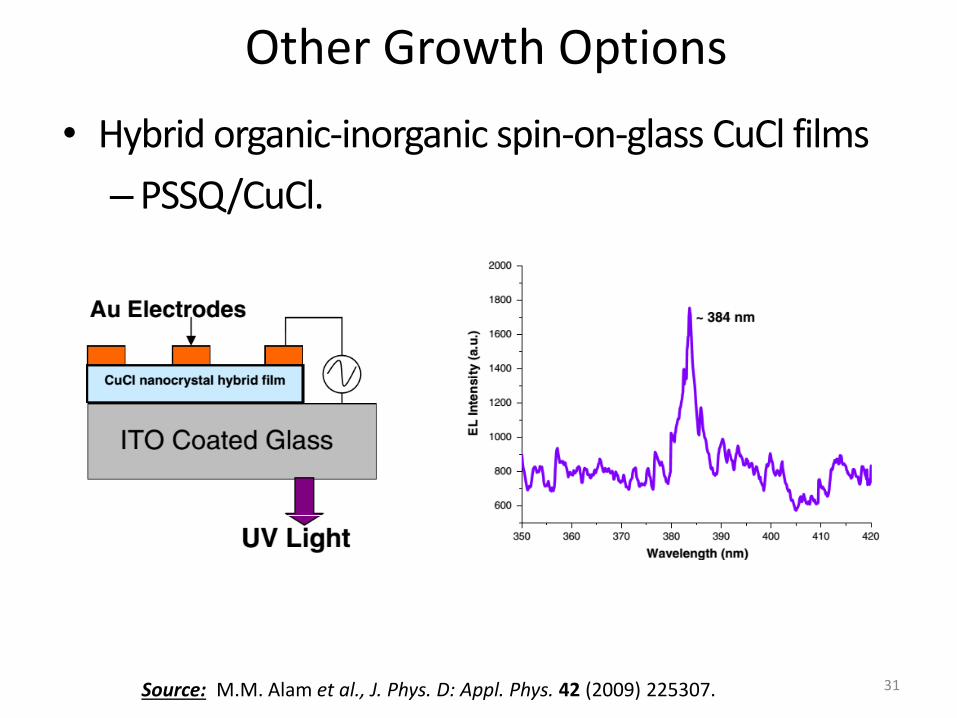
Other Growth Options
• Hybrid organic-inorganic spin-on-glass CuCl films
–PSSQ/CuCl.
Source: M.M. Alam et al., J. Phys. D: Appl. Phys. 42 (2009) 225307. 31
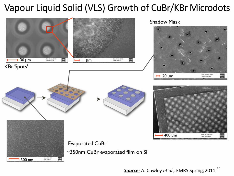
Vapour Liquid Solid (VLS) Growth of CuBr/KBr Microdots
30 μm 1 μm
Shadow Mask
KBr ‘Spots’
20 μm
400 μm
Evaporated CuBr
~350nm CuBr evaporated film on Si
300 nm
Source: A. Cowley et al., EMRS Spring, 2011. 32
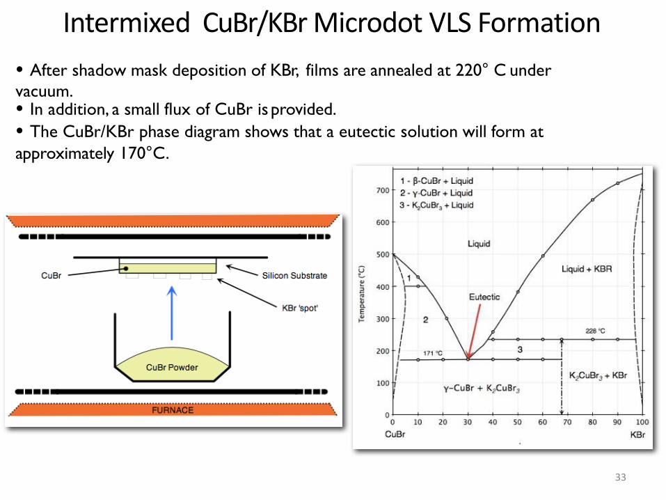
Intermixed CuBr/KBr Microdot VLS Formation
• After shadow mask deposition of KBr, films are annealed at 220° C under
vacuum. • In addition, a small flux of CuBr is provided.
• The CuBr/KBr phase diagram shows that a eutectic solution will form at
approximately 170°C.
33
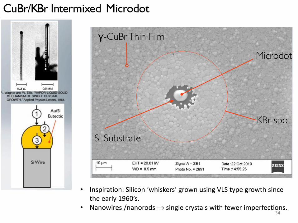
CuBr/KBr Intermixed Microdot
• Inspiration: Silicon ‘whiskers’ grown using VLS type growth since the early 1960’s.
• Nanowires /nanorods single crystals with fewer imperfections.
34
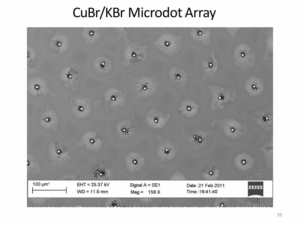
CuBr/KBr Microdot Array
35
425 390
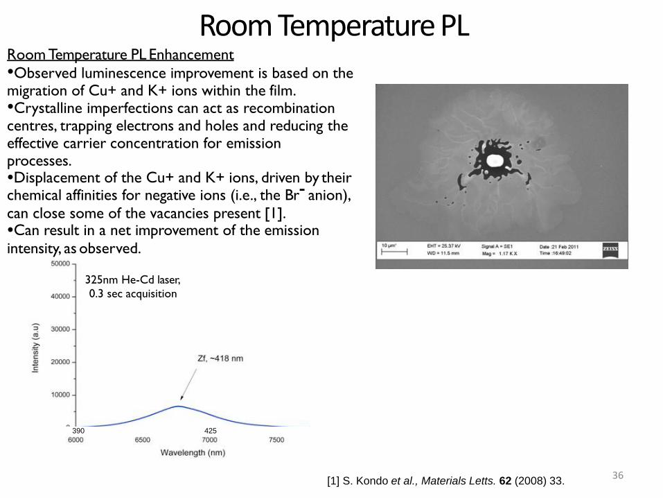
Room Temperature PL Room Temperature PL Enhancement
•Observed luminescence improvement is based on the migration of Cu+ and K+ ions within the film. •Crystalline imperfections can act as recombination centres, trapping electrons and holes and reducing the effective carrier concentration for emission processes. •Displacement of the Cu+ and K+ ions, driven by their chemical affinities for negative ions (i.e., the Br- anion),
can close some of the vacancies present [1]. •Can result in a net improvement of the emission
intensity, as observed.
325nm He-Cd laser,
0.3 sec acquisition
36 [1] S. Kondo et al., Materials Letts. 62 (2008) 33.
425 390
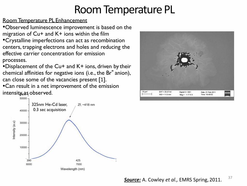
Room Temperature PL Enhancement
•Observed luminescence improvement is based on the migration of Cu+ and K+ ions within the film •Crystalline imperfections can act as recombination centers, trapping electrons and holes and reducing the effective carrier concentration for emission processes. •Displacement of the Cu+ and K+ ions, driven by their chemical affinities for negative ions (i.e., the Br- anion), can close some of the vacancies present [1].
•Can result in a net improvement of the emission
intensity, as observed.
325nm He-Cd laser,
0.3 sec acquisition
Room Temperature PL
37 Source: A. Cowley et al., EMRS Spring, 2011.
Where next? • Excellent progress in CuHa materials processing in past decade.
• Opportunity to develop new science, technology and devices.
• Quantum manipulation of light and matter for blue/UV (350-450 nm).
• Electrically pumped microcavity structures.
• Ultralow power blue/UV light emitters. – Exciton, biexciton and polariton control.
– Potential for quantum entanglement.
• Applications: – Medical and biodiagnostics: new capability in point of care diagnostics;
– Computing : extremely low power optical interconnects;
– Telecommunications: THz speed optical spin switching;
– Security/cryptography: quantum entanglement for quantum information processing communications;
– Who knows??? 38

THANK YOU!!!
39
40
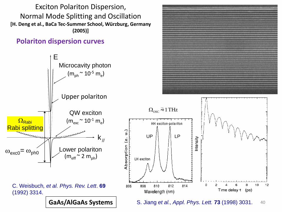
Polariton dispersion curves
osc~ 1 THz
C. Weisbuch, et al. Phys. Rev. Lett. 69
(1992) 3314.
S. Jiang et al., Appl. Phys. Lett. 73 (1998) 3031.
Exciton Polariton Dispersion, Normal Mode Splitting and Oscillation
[H. Deng et al., BaCa Tec-Summer School, Würzburg, Germany (2005)]
UP LP
OSC 1THz ~
GaAs/AlGaAs Systems
Rabi
Rabi splitting
wexc0 = wph0
E
k //
QW exciton
Lower polariton
Upper plariton
Microcavity photon
(mph ~ 10-5 me)
(mexc ~ 10-1 me)
(meff ~ 2 mph)
Upper polariton
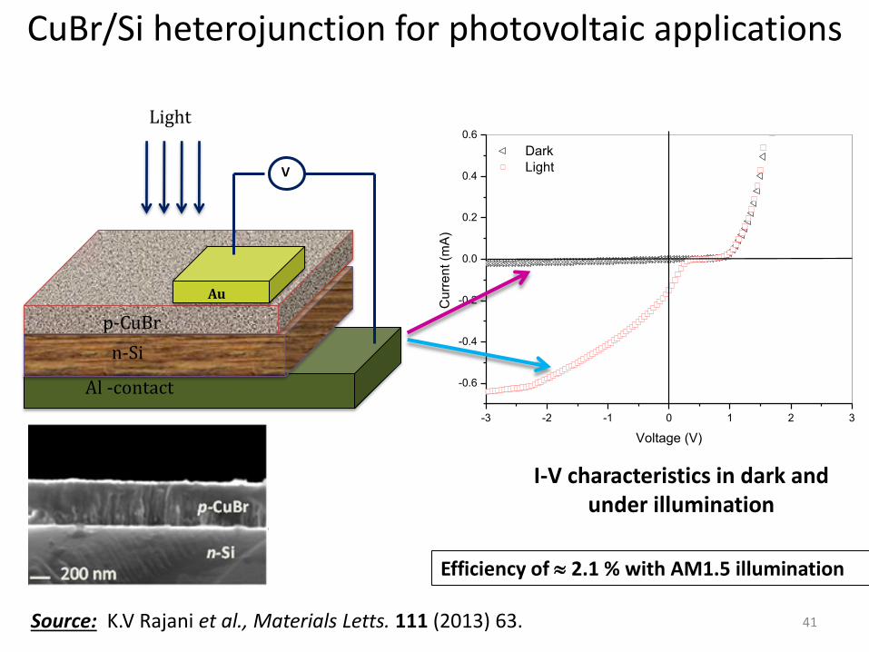
CuBr/Si heterojunction for photovoltaic applications
Al -contact
p-CuBr
Au
n-Si
-3 -2 -1 0 1 2 3
-0.6
-0.4
-0.2
0.0
0.2
0.4
0.6
Dark
Light
Cu
rre
nt (m
A)
Voltage (V)
I-V characteristics in dark and under illumination
V
Light
Source: K.V Rajani et al., Materials Letts. 111 (2013) 63.
Efficiency of 2.1 % with AM1.5 illumination
41
42
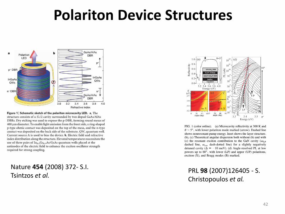
Nature 454 (2008) 372- S.I. Tsintzos et al.
PRL 98 (2007)126405 - S. Christopoulos et al.
Polariton Device Structures
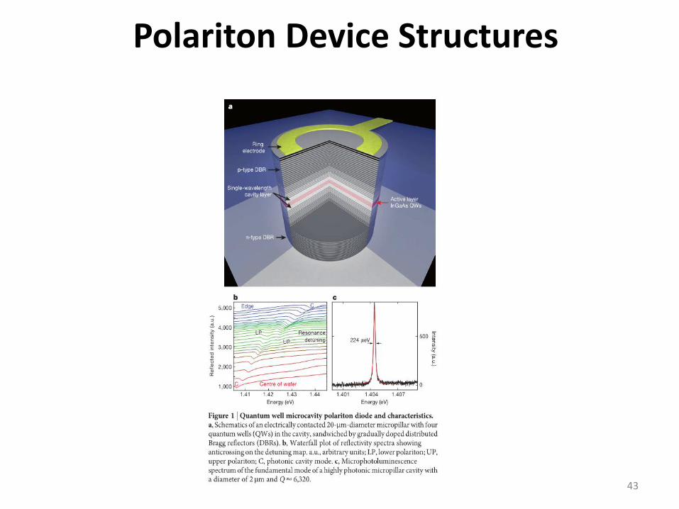
Polariton Device Structures
43