Embed Size (px)
Citation preview
CONVERTING THREE-STAGE PSEUDO-CLASS AB AMPLIFIERS TO
TRUE CLASS AB AMPLIFIERS
BY
PUNITH REDDY SURKANTI, B.Tech
A dissertation submitted to the Graduate School
in partial fulfillment of the requirements
for the degree
Master of Sciences, Engineering
Specialization in: Electrical Engineering
New Mexico State University
Las Cruces, New Mexico
March 2011

“CONVERTING THREE-STAGE PSEUDO-CLASS AB AMPLIFIERS TO TRUE
CLASS AB AMPLIFIERS,” a dissertation prepared by PUNITH REDDY SURKANTI in
partial fulfillment of the requirements for the degree, Master of Sciences has been
approved and accepted by the following:
Linda LaceyDean of the Graduate School
Chair of the Examining Committee
Date
Committee in charge:
Dr. Paul M. Furth, Associate Professor, Chair.
Dr. Jaime Ramirez-Angulo, Professor.
Dr. Jeffery Beasley, Professor.
ii
DEDICATION
Dedicated to my mother Lalitha, father Madhava Reddy, sister Dr. Avanthi
Reddy, my advisor Dr. Paul Furth and all my friends and family members.
iii
ACKNOWLEDGMENTS
I would like to thank my parents Lalitha Surkanti and Madhava Reddy
Surkanti for their support and their confidence. And my sister Dr. Avanthi
Reddy Surkanti, who encouraged me to complete my Master’s in USA. She is a
role model for me, who inspired me for what I have done.
A teacher is treated as a god next to our patents. I thank Dr. Paul M.
Furth for advising me throughout my Master’s degree. I learned much from his
teaching through courses like digital VLSI and Image Sensors; learned how to
do research and research philosophy through his research. I assisted Dr. Furth
in preparing lectures for a course titled EE590: Integrated Power Management.
During that time, I learned the teaching skills, how to prepare lectures, how to
think and how to explain so that the students can understand. All of this has
helped me in explaining concepts to the students. I thank his family with whom
we spent time on Thanksgiving day every year. We play sports and fun games
and had some good food on that day. I will never forget those memories.
Great appreciation and thanks to Dr. Jaime Ramirez-Angulo for accepting
my request to be a member of my thesis committee. I took two major VLSI courses
under him which helped me in learning good concepts in analog design. He is a
good and energetic professor and helped a lot during our labs. I wish that I can
work with him in collaborated research to know his research type and philosophy.
iv

Beyond his busy schedule as a head of the department for Engineering
Technology, I thank Dr. Jeffery Beasley for accepting my request to be a member
of my thesis committee.
Thanks to my cousins, Vineela, Nithin, Prathyusha, Panchi, Pranaya,
Pravalika, Sanvitha, Maninder and all my relatives.
I would like to thank my undergraduate friends, Nevil Kranthi, Dhanun-
jay Reddy, Ram Reddy, Bharath Reddy, Rajiv Reddy, Nikhil Reddy, Raj kumar,
Rajesh, Naresh Reddy, Manoj, Shashank, Kamesh, Shyam, Vinod.
I would like to thank my seniors in las cruces, Pulla Reddy, Koushik, An-
najirao, Wasequer, Praneeth. They helped me learning concepts in VLSI and
choosing my research.
Thanks to my friends in las cruces, Chaitanya Mohan, Harish Valapala,
Rajesh, Ramesh, Venkat Reddy, Nikhilesh, Suresh, Karunakar, Arun, Sandeep,
Santhosh SK, Varun, Sravan, Lalith, Venugopal, Madhusudhan Reddy, Srini-
vasu Pudi, Vamshidhar Reddy, Srikanth Reddy, Sriharsh, Harish Nammi, Nitya,
Chayya, Sailaja. I would like to thank all the members of Indian Student Associ-
ation (ISA) for supporting me.
Thanks to Adam Crittenden for correcting grammar, tense and spellings
in my thesis report.
v
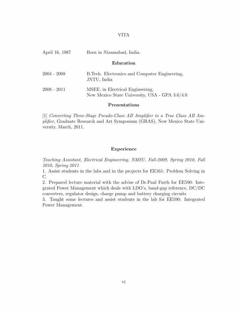
VITA
April 16, 1987 Born in Nizamabad, India.
Education
2004 - 2008 B.Tech. Electronics and Computer Engineering,JNTU, India
2008 - 2011 MSEE. in Electrical Engineering,New Mexico State University, USA - GPA 3.6/4.0
Presentations
[1] Converting Three-Stage Pseudo-Class AB Amplifier to a True Class AB Am-plifier, Graduate Research and Art Symposium (GRAS), New Mexico State Uni-versity, March, 2011.
Experience
Teaching Assistant, Electrical Engineering, NMSU, Fall-2009, Spring 2010, Fall2010, Spring 20111. Assist students in the labs and in the projects for EE161: Problem Solving inC.2. Prepared lecture material with the advise of Dr.Paul Furth for EE590: Inte-grated Power Management which deals with LDO’s, band-gap reference, DC/DCconverters, regulator design, charge pump and battery charging circuits3. Taught some lectures and assist students in the lab for EE590: IntegratedPower Management.
vi
ABSTRACT
CONVERTING THREE-STAGE PSEUDO-CLASS AB AMPLIFIERS TO
TRUE CLASS AB AMPLIFIERS
BY
PUNITH REDDY SURKANTI, B.Tech
Master of Sciences, Engineering
Specialization in Electrical Engineering
New Mexico State University
Las Cruces, New Mexico, 2011
Dr. Paul M. Furth, Chair
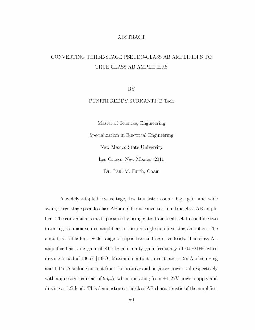
A widely-adopted low voltage, low transistor count, high gain and wide
swing three-stage pseudo-class AB amplifier is converted to a true class AB ampli-
fier. The conversion is made possible by using gate-drain feedback to combine two
inverting common-source amplifiers to form a single non-inverting amplifier. The
circuit is stable for a wide range of capacitive and resistive loads. The class AB
amplifier has a dc gain of 81.7dB and unity gain frequency of 6.58MHz when
driving a load of 100pF||10kΩ. Maximum output currents are 1.12mA of sourcing
and 1.14mA sinking current from the positive and negative power rail respectively
with a quiescent current of 95µA, when operating from ±1.25V power supply and
driving a 1kΩ load. This demonstrates the class AB characteristic of the amplifier.
vii
Both pseudo-class AB and true class AB amplifiers were fabricated in a 0.5µm
CMOS 2P3M technology and measured to characterize their differences.
A novel inverting current buffer compensation technique for multi-stage
amplifiers is proposed. The compensation capacitor from the output is connected
to the bias node that helps in increasing the bandwidth and improving the power
supply rejection ratio. This also helps in increasing the driving capability for a
wide range of load capacitor values.
viii
TABLE OF CONTENTS
LIST OF TABLES xii
LIST OF FIGURES xiii
1 INTRODUCTION 1
2 LITERATURE REVIEW 4
2.1 Multi-Stage Amplifiers . . . . . . . . . . . . . . . . . . . . . . . . 4
2.2 Compensation Techniques . . . . . . . . . . . . . . . . . . . . . . 5
2.2.1 Miller Compensation . . . . . . . . . . . . . . . . . . . . . 5
2.2.2 Ahuja Compensation . . . . . . . . . . . . . . . . . . . . . 7
2.2.3 Nested Miller Compensation . . . . . . . . . . . . . . . . . 8
2.2.4 Reverse-Nested Miller Compensation . . . . . . . . . . . . 9
2.2.5 Miller Compensation with Inverted Current-Buffer . . . . . 10
2.3 Class AB Amplifiers . . . . . . . . . . . . . . . . . . . . . . . . . 11
2.3.1 I-I-N Pseudo Class-AB Amplifier [1] . . . . . . . . . . . . . 11
2.3.2 Pseudo-Class AB to True Class AB Amplifier using Adap-tive Biasing proposed in [2] . . . . . . . . . . . . . . . . . 13
3 DESIGN AND SIMULATIONS 15
3.1 I-I-N Three-stage Pseudo-Class AB Amplifier . . . . . . . . . . . 15
3.1.1 Operation . . . . . . . . . . . . . . . . . . . . . . . . . . . 15
ix
3.1.2 Small-Signal Analysis . . . . . . . . . . . . . . . . . . . . . 17
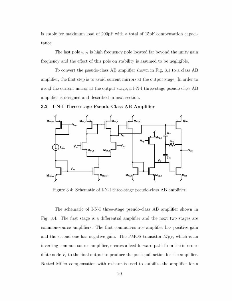
3.2 I-N-I Three-stage Pseudo-Class AB Amplifier . . . . . . . . . . . 20
3.2.1 Operation . . . . . . . . . . . . . . . . . . . . . . . . . . . 21
3.2.2 Small-Signal Analysis . . . . . . . . . . . . . . . . . . . . . 23
3.3 Inverted Current-Buffer Compensation . . . . . . . . . . . . . . . 25
3.3.1 Inverted Current Buffer . . . . . . . . . . . . . . . . . . . 25
3.3.2 Small-Signal Model . . . . . . . . . . . . . . . . . . . . . . 28
3.4 Simulation Results Compared with Inverted Current-Buffer Com-pensation . . . . . . . . . . . . . . . . . . . . . . . . . . . . . . . 29
3.4.1 AC Analysis . . . . . . . . . . . . . . . . . . . . . . . . . . 32
3.4.2 Transient Analysis . . . . . . . . . . . . . . . . . . . . . . 32
3.4.3 Power-Supply Rejection Ratio . . . . . . . . . . . . . . . . 34
3.5 I-N-I Three-stage Class AB Amplifier . . . . . . . . . . . . . . . . 37
3.5.1 Operation . . . . . . . . . . . . . . . . . . . . . . . . . . . 38
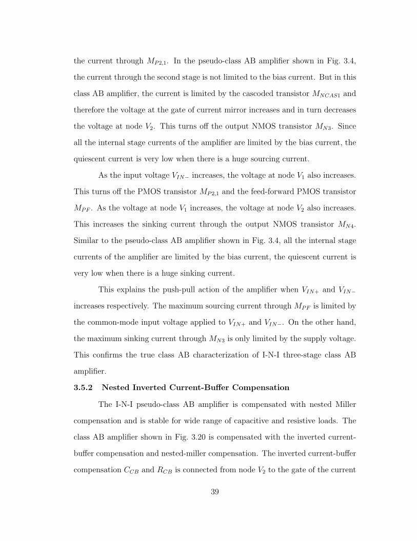
3.5.2 Nested Inverted Current-Buffer Compensation . . . . . . . 39
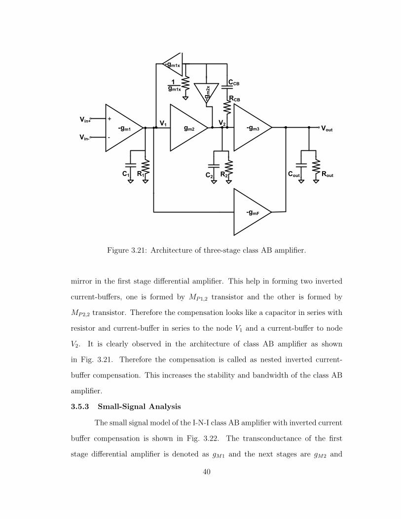
3.5.3 Small-Signal Analysis . . . . . . . . . . . . . . . . . . . . . 40
3.6 Proposed Three-stage True Class AB Amplifier . . . . . . . . . . 43
3.6.1 Gate-Drain Feedback . . . . . . . . . . . . . . . . . . . . . 44
3.6.2 Operation . . . . . . . . . . . . . . . . . . . . . . . . . . . 45
3.6.3 Nullified Effect of Inverted Current-Buffer Compensation . 46
3.6.4 Small-Signal Analysis . . . . . . . . . . . . . . . . . . . . . 47
3.7 Simulation Results Compared with the Proposed Class AB Amplifier 48
3.7.1 DC Analysis . . . . . . . . . . . . . . . . . . . . . . . . . . 49
3.7.2 AC Analysis . . . . . . . . . . . . . . . . . . . . . . . . . . 52
3.7.3 Transient Analysis . . . . . . . . . . . . . . . . . . . . . . 54
x
4 EXPERIMENTAL RESULTS 57
4.1 Layout . . . . . . . . . . . . . . . . . . . . . . . . . . . . . . . . . 57
4.2 Test apparatus . . . . . . . . . . . . . . . . . . . . . . . . . . . . 60
4.3 Hardware Transient Result . . . . . . . . . . . . . . . . . . . . . . 61
4.3.1 I-I-N Three-Stage Pseudo-Class AB Amplifier . . . . . . . 61
4.3.2 I-I-N Three-Stage Pseudo-Class AB Amplifier with Invert-ing Current-Buffer Compensation . . . . . . . . . . . . . . 62
4.3.3 I-N-I Three-Stage Pseudo-Class AB Amplifier . . . . . . . 63
4.3.4 Proposed Three-Stage True Class AB Amplifier . . . . . . 63
4.4 Measurement Results . . . . . . . . . . . . . . . . . . . . . . . . . 63
5 DISCUSSION AND CONCLUSION 66
5.0.1 Issues . . . . . . . . . . . . . . . . . . . . . . . . . . . . . 67
5.0.2 Anomalies . . . . . . . . . . . . . . . . . . . . . . . . . . . 67
5.0.3 Future Work . . . . . . . . . . . . . . . . . . . . . . . . . . 67
APPENDICES 69
A. Test Document 70
A.1 Supply Voltages and Currents . . . . . . . . . . . . . . . . . . . . 71
A.2 Procedure . . . . . . . . . . . . . . . . . . . . . . . . . . . . . . . 71
B. Maple 80
REFERENCES 82
xi
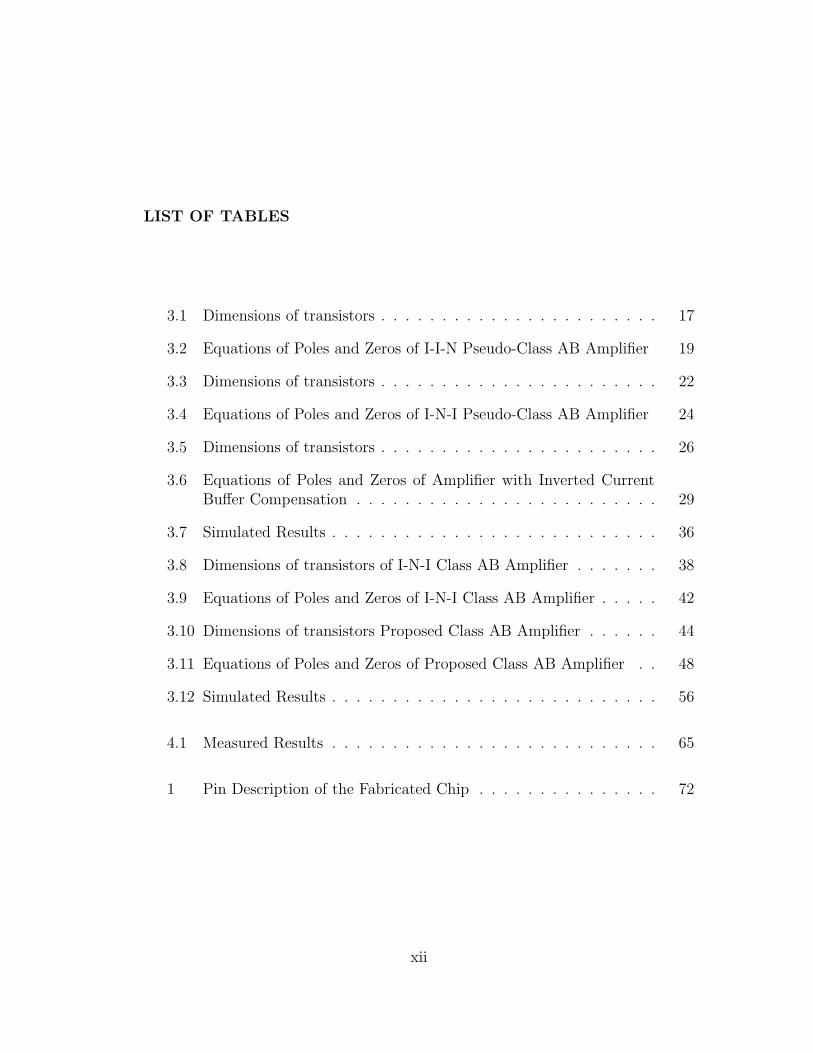
LIST OF TABLES
3.1 Dimensions of transistors . . . . . . . . . . . . . . . . . . . . . . . 17
3.2 Equations of Poles and Zeros of I-I-N Pseudo-Class AB Amplifier 19
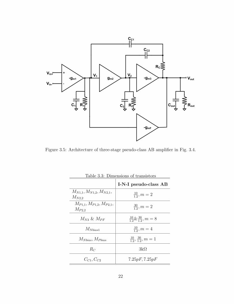
3.3 Dimensions of transistors . . . . . . . . . . . . . . . . . . . . . . . 22
3.4 Equations of Poles and Zeros of I-N-I Pseudo-Class AB Amplifier 24
3.5 Dimensions of transistors . . . . . . . . . . . . . . . . . . . . . . . 26
3.6 Equations of Poles and Zeros of Amplifier with Inverted CurrentBuffer Compensation . . . . . . . . . . . . . . . . . . . . . . . . . 29
3.7 Simulated Results . . . . . . . . . . . . . . . . . . . . . . . . . . . 36
3.8 Dimensions of transistors of I-N-I Class AB Amplifier . . . . . . . 38
3.9 Equations of Poles and Zeros of I-N-I Class AB Amplifier . . . . . 42
3.10 Dimensions of transistors Proposed Class AB Amplifier . . . . . . 44
3.11 Equations of Poles and Zeros of Proposed Class AB Amplifier . . 48
3.12 Simulated Results . . . . . . . . . . . . . . . . . . . . . . . . . . . 56
4.1 Measured Results . . . . . . . . . . . . . . . . . . . . . . . . . . . 65
1 Pin Description of the Fabricated Chip . . . . . . . . . . . . . . . 72
xii
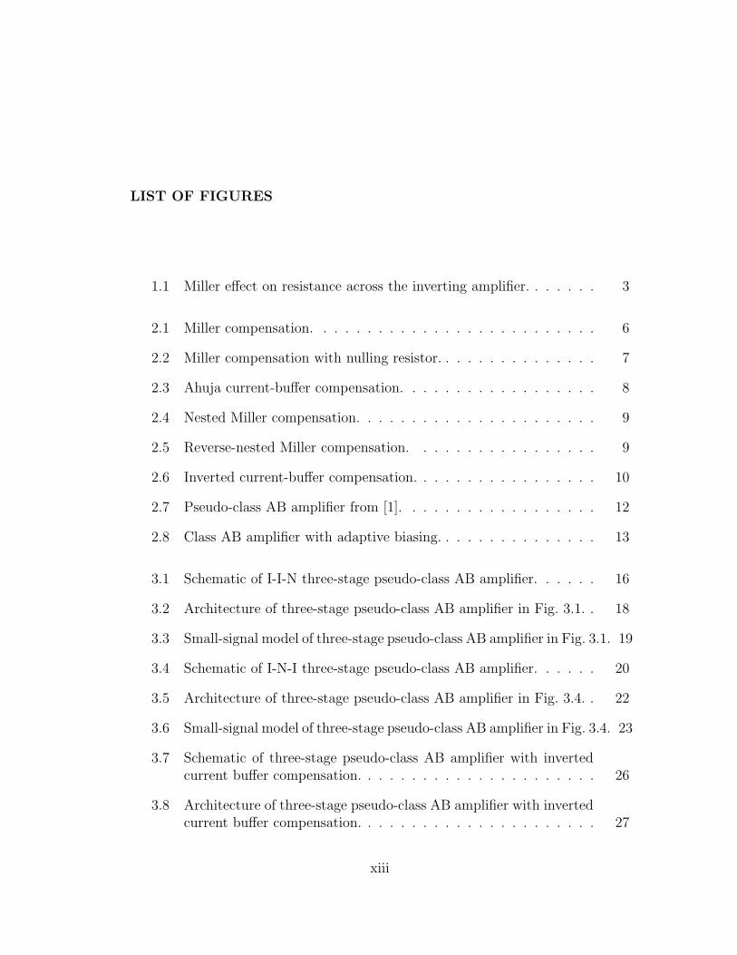
LIST OF FIGURES
1.1 Miller effect on resistance across the inverting amplifier. . . . . . . 3
2.1 Miller compensation. . . . . . . . . . . . . . . . . . . . . . . . . . 6
2.2 Miller compensation with nulling resistor. . . . . . . . . . . . . . . 7
2.3 Ahuja current-buffer compensation. . . . . . . . . . . . . . . . . . 8
2.4 Nested Miller compensation. . . . . . . . . . . . . . . . . . . . . . 9
2.5 Reverse-nested Miller compensation. . . . . . . . . . . . . . . . . 9
2.6 Inverted current-buffer compensation. . . . . . . . . . . . . . . . . 10
2.7 Pseudo-class AB amplifier from [1]. . . . . . . . . . . . . . . . . . 12
2.8 Class AB amplifier with adaptive biasing. . . . . . . . . . . . . . . 13
3.1 Schematic of I-I-N three-stage pseudo-class AB amplifier. . . . . . 16
3.2 Architecture of three-stage pseudo-class AB amplifier in Fig. 3.1. . 18
3.3 Small-signal model of three-stage pseudo-class AB amplifier in Fig. 3.1. 19
3.4 Schematic of I-N-I three-stage pseudo-class AB amplifier. . . . . . 20
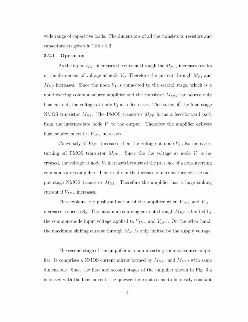
3.5 Architecture of three-stage pseudo-class AB amplifier in Fig. 3.4. . 22
3.6 Small-signal model of three-stage pseudo-class AB amplifier in Fig. 3.4. 23
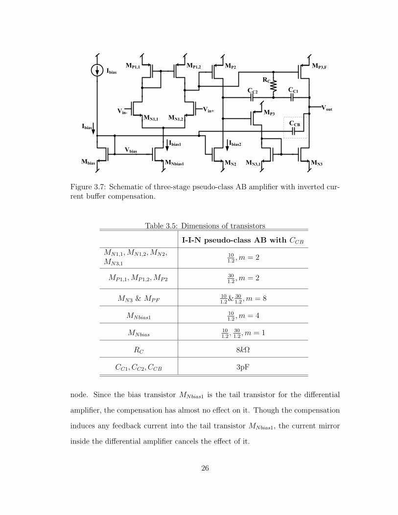
3.7 Schematic of three-stage pseudo-class AB amplifier with invertedcurrent buffer compensation. . . . . . . . . . . . . . . . . . . . . . 26
3.8 Architecture of three-stage pseudo-class AB amplifier with invertedcurrent buffer compensation. . . . . . . . . . . . . . . . . . . . . . 27
xiii
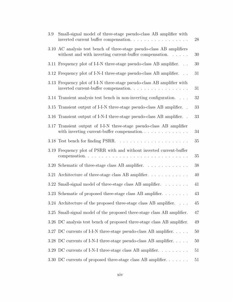
3.9 Small-signal model of three-stage pseudo-class AB amplifier withinverted current buffer compensation. . . . . . . . . . . . . . . . . 28
3.10 AC analysis test bench of three-stage pseudo-class AB amplifierswithout and with inverting current-buffer compensation. . . . . . 30
3.11 Frequency plot of I-I-N three-stage pseudo-class AB amplifier. . . 30
3.12 Frequency plot of I-N-I three-stage pseudo-class AB amplifier. . . 31
3.13 Frequency plot of I-I-N three-stage pseudo-class AB amplifier withinverted current-buffer compensation. . . . . . . . . . . . . . . . . 31
3.14 Transient analysis test bench in non-inverting configuration. . . . 32
3.15 Transient output of I-I-N three-stage pseudo-class AB amplifier. . 33
3.16 Transient output of I-N-I three-stage pseudo-class AB amplifier. . 33
3.17 Transient output of I-I-N three-stage pseudo-class AB amplifierwith inverting current-buffer compensation. . . . . . . . . . . . . . 34
3.18 Test bench for finding PSRR. . . . . . . . . . . . . . . . . . . . . 35
3.19 Frequency plot of PSRR with and without inverted current-buffercompensation. . . . . . . . . . . . . . . . . . . . . . . . . . . . . . 35
3.20 Schematic of three-stage class AB amplifier. . . . . . . . . . . . . 38
3.21 Architecture of three-stage class AB amplifier. . . . . . . . . . . . 40
3.22 Small-signal model of three-stage class AB amplifier. . . . . . . . 41
3.23 Schematic of proposed three-stage class AB amplifier. . . . . . . . 43
3.24 Architecture of the proposed three-stage class AB amplifier. . . . 45
3.25 Small-signal model of the proposed three-stage class AB amplifier. 47
3.26 DC analysis test bench of proposed three-stage class AB amplifier. 49
3.27 DC currents of I-I-N three-stage pseudo-class AB amplifier. . . . . 50
3.28 DC currents of I-N-I three-stage pseudo-class AB amplifier. . . . . 50
3.29 DC currents of I-N-I three-stage class AB amplifier. . . . . . . . . 51
3.30 DC currents of proposed three-stage class AB amplifier. . . . . . . 51
xiv
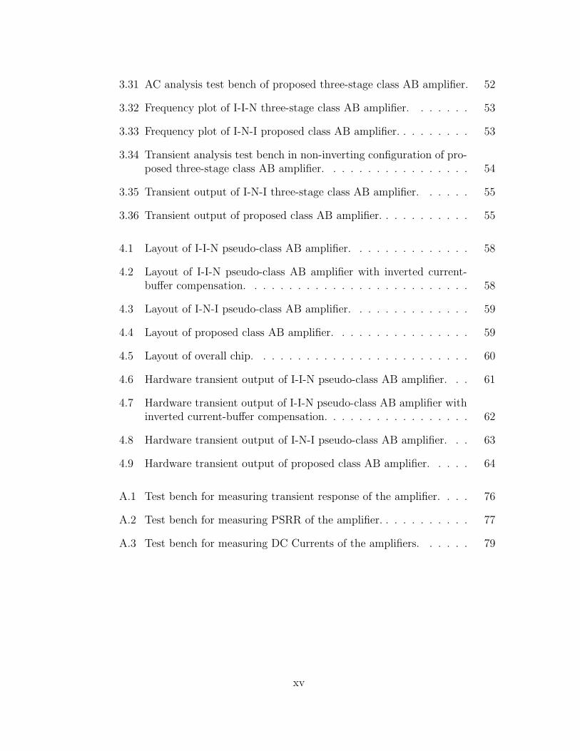
3.31 AC analysis test bench of proposed three-stage class AB amplifier. 52
3.32 Frequency plot of I-I-N three-stage class AB amplifier. . . . . . . 53
3.33 Frequency plot of I-N-I proposed class AB amplifier. . . . . . . . . 53
3.34 Transient analysis test bench in non-inverting configuration of pro-posed three-stage class AB amplifier. . . . . . . . . . . . . . . . . 54
3.35 Transient output of I-N-I three-stage class AB amplifier. . . . . . 55
3.36 Transient output of proposed class AB amplifier. . . . . . . . . . . 55
4.1 Layout of I-I-N pseudo-class AB amplifier. . . . . . . . . . . . . . 58
4.2 Layout of I-I-N pseudo-class AB amplifier with inverted current-buffer compensation. . . . . . . . . . . . . . . . . . . . . . . . . . 58
4.3 Layout of I-N-I pseudo-class AB amplifier. . . . . . . . . . . . . . 59
4.4 Layout of proposed class AB amplifier. . . . . . . . . . . . . . . . 59
4.5 Layout of overall chip. . . . . . . . . . . . . . . . . . . . . . . . . 60
4.6 Hardware transient output of I-I-N pseudo-class AB amplifier. . . 61
4.7 Hardware transient output of I-I-N pseudo-class AB amplifier withinverted current-buffer compensation. . . . . . . . . . . . . . . . . 62
4.8 Hardware transient output of I-N-I pseudo-class AB amplifier. . . 63
4.9 Hardware transient output of proposed class AB amplifier. . . . . 64
A.1 Test bench for measuring transient response of the amplifier. . . . 76
A.2 Test bench for measuring PSRR of the amplifier. . . . . . . . . . . 77
A.3 Test bench for measuring DC Currents of the amplifiers. . . . . . 79
xv
Chapter 1
INTRODUCTION
Class AB amplifiers have a wide range of applications in portable electronic de-
vices. They are used in the design of circuits such as audio amplifiers, motor
drivers and LED & LCD drivers [3]. Most of these applications require class AB
amplifiers with low power, high efficiency, and stability for a wide range of loads.
A widely-adopted low voltage, low transistor-count, high-gain and wide-
swing three-stage pseudo-class AB amplifier is proposed in [1]. We designed a
NMOS version of that pseudo-classs AB amplifier and analysed the circuit using
the location of poles and zeros. We introduced a novel inverted current-buffer
compensation to that pseudo class AB amplifier to increase stability with low
compensation capacitor values. Inverted current-buffer helps in inserting a LHP
zero and improves phase margin. The inverted current-buffer compensation also
helps in increasing Power-Supply Rejection Ratio (PSRR).
The pseudo-class AB amplifier has inverting, inverting and non-inverting
gain cascaded stages. The pseudo-class AB amplifier has a NMOS current mirror
in the output-stage and, therefore, the quiescent current increases with the out-
put sinking current. We re-designed the circuit with same number of transistors
and removed the current mirror in the output stage. The modified amplifier has
inverting, non-inverting and inverting gain cascaded stages. The drawback of this
amplifier is the quiescent current increase with the increase in output sourcing cur-
1

rent. This is because of the huge current through the second-stage common-source
amplifier.
We limited the current in the second stage to the bias current by adding the
cascoded transistors to the current mirror. The new design has nearly constant
quiescent current irrespective of changes in the the output current. Therefore,
this amplifier is designated as a true class AB amplifier. The class AB amplifier
is stable with nested inverting current-buffer compensation for wide range of load
capacitance. But the drawback of this class AB amplifier is that the quiescent for
sourcing current is slightly higher than the quiescent current for sinking current.
This is because of the cascoded current mirror in the second-stage.
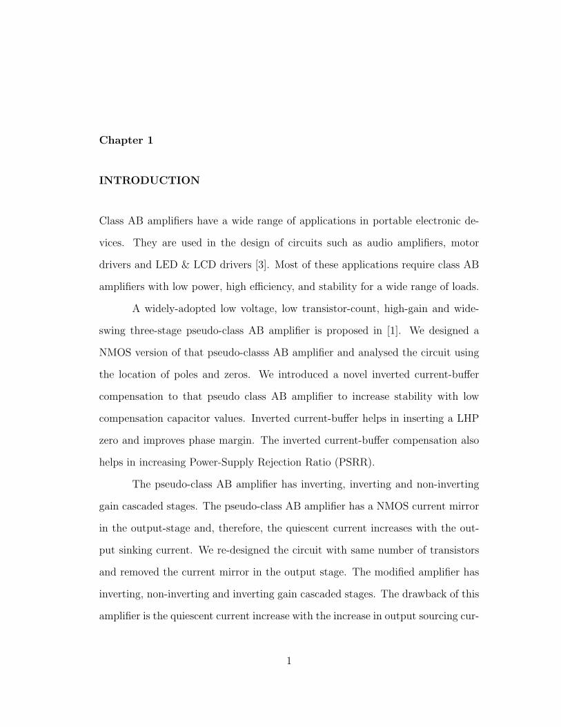
Finally, we proposed a true class AB amplifier which has inverting, non-
inverting and inverting gain cascade stages. The non-inverting common-source
stage is designed by using gate-drain feedback to combine two inverting common-
source amplifiers. Gate-drain feedback resistor across the inverting common-
source amplifier helps in cancelling its effect for the overall second-stage. Miller
effect splits the impedance across the amplifier to input node and output node as
shown in Fig. 1.1. Therefore, the resistor to the input side decreases by the gain
of the amplifier. If this amplifier is cascaded to an amplifier, then the gain of first
stage is cancelled. This is because of the decrement of the resistor value by gain
of the next amplifier; therefore, the overall gain is positive.
The proposed class AB amplifier is compensated with both nested and
reverse-nested Miller compensation to increase the stability. The inverted current-
buffer compensation has no effect for this amplifier because of forming both neg-
ative and positive feedback network with the proposed compensation capacitor.
Since current through all the internal stages are limited to the bias current,
the total quiescent current is nearly constant irrespective of the output current.
2
Vout-AVVin
Vout-AVVin
RC
RC
(1+AV)RC[1+(1/AV)]
Figure 1.1: Miller effect on resistance across the inverting amplifier.
Unlike the class AB amplifier discussed earlier, the proposed class AB amplifier
has the same quiescent current for both sourcing and sinking current.
The proposed class AB is stable for a wide range of capacitive and resistive
loads. The bandwidth of the proposed class AB amplifier is increased by 60%
when compared to the I-I-N pseudo-class AB amplifier and 25% compared to the
pseudo-class AB amplifier with inverting current buffer compensation. Maximum
output currents are 1.12mA of sourcing and 1.14mA sinking current from the
positive and negative power rail respectively for all the amplifiers when operating
from ±1.25V power supply and driving a 1kΩ load. The maximum quiescent
current of I-I-N and I-N-I pseudo-class AB amplifier is nearly 300µA and 483µA,
respectively. The maximum quiescent current of proposed class AB amplifier is
nearly 95µA. This demonstrates the true class AB characteristic of the proposed
amplifier. All the amplifiers are fabricated in a 0.5µm CMOS 2P3M technology
and measured to characterize their differences.
3
Chapter 2
LITERATURE REVIEW
This section discusses the work done in the literature. The different types of com-
pensation techniques used for multi-stage amplifiers, class AB amplifiers, pseudo-
class AB amplifiers and a topology in literature to convert pseudo-class AB am-
plifier to a true class AB amplifier.
2.1 Multi-Stage Amplifiers
As technology advances, parameters such as size of the transistor and sup-
ply voltage are decreasing. This results in the reduction in gain for a single-stage
amplifier. The best method to achieve high gain is by cascading amplifiers, where
the total gain is the product of gains of each stage. The output-swing is maxi-
mized for common-source output stages, resulting in rail-to-rail output swing [4].
However, as the number of stages increases, the stability of the overall amplifier
becomes more difficult to guarantee for a wide range of capacitive loads.
An amplifier is said to be stable, if the gain crosses unity before the phase
drops to -180o. The maximum available phase at unity-gain frequency (ft) is
known as the phase margin. Phase margin helps in determining stability; 60o of
phase margin typically implies a stable system with fast time-domain response
and little to one ringing. 45o of phase margin implies some ringing in the time-
domain response. Less than 45o is considered undesirable, as ringing increases
and normal variations in process parameters could result in an unstable system.
4

The number and position of poles and zeros effects the phase margin. The
number of poles increases with the number of cascaded stages. Left-Half-Plane
(LHP) poles decrease the gain with a slope of -20dB/decade and drops the phase
by 90o. If a system has two low frequency poles, then the phase drops towards
-180o before the gain cross ft. This makes the system unstable. LHP zeros are
inserted to improve the stability. A LHP zero increases the gain by 20dB/decade
and increases the phase by 90o. If a system with two poles has a LHP zero,
then the effect of one of the poles is cancelled by proper placement of the zero.
If cancellation is not possible, then the zero often helps in improving the phase
margin.
Compensation techniques are used to split the poles and to insert the zeros.
Careful compensation helps in guaranteeing stability of the overall amplifier for
a wide range of capacitive loads. The complexity of the compensation network
increases with the number of cascaded stages [5]. Different compensation tech-
niques are used to improve the stability and some of them are discussed in the
next section.
2.2 Compensation Techniques
Amplifiers are compensated in different manners, depending on the num-
ber of stages. Miller compensation and Ahuja compensation are used in am-
plifiers with two or more cascaded stages, whereas, nested Miller compensation
and reverse-nested Miller compensation are used in amplifiers with three or more
cascaded stages.
2.2.1 Miller Compensation
Miller compensation is widely used and discussed in literature [6, 4, 7, 8]
Miller compensation is used in a two-stage amplifier as shown in Fig. 2.1. A ca-
pacitor CC is connected between output node and the internal node V1. This splits
5

-AV1
Vin+
Vout
+
-
-AV2
CC
ROutCOut
Vin-
V1
R1C1
Figure 2.1: Miller compensation.
the two poles; the dominant one to lower frequencies and the non-dominant one to
higher frequencies. The existence of a feed-forward path from V1 to VOUT creates
a Right-Half-Plane (RHP) zero. A RHP zero increases the gain by 20dB/decade
and drops the phase by 90o. RHP zeros are more dangerous than LHP poles, as
they tend to decrease the phase margin. The equation of two LHP poles is
ωP1 =1
AV 2 ·R1 · CC
. (2.1)
ωP2 =AV 2
(R1 +RC) · COUT
. (2.2)
6
-AV1
Vin+
Vout
+
-
-AV2
CC RC
ROutCOut
Vin-
V1
R1C1
Figure 2.2: Miller compensation with nulling resistor.
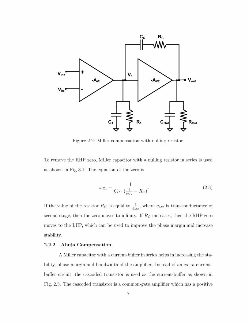
To remove the RHP zero, Miller capacitor with a nulling resistor in series is used
as shown in Fig 3.1. The equation of the zero is
ωZ1 =1
CC · ( 1gM2−RC)
. (2.3)
If the value of the resistor RC is equal to 1gM2
, where gM2 is transconductance of
second stage, then the zero moves to infinity. If RC increases, then the RHP zero
moves to the LHP, which can be used to improve the phase margin and increase
stability.
2.2.2 Ahuja Compensation
A Miller capacitor with a current-buffer in series helps in increasing the sta-
bility, phase margin and bandwidth of the amplifier. Instead of an extra current-
buffer circuit, the cascoded transistor is used as the current-buffer as shown in
Fig. 2.3. The cascoded transistor is a common-gate amplifier which has a positive
7

MP1,1 MP1,2
MN1,1 MN1,2
MNbias1
Vbias
Vin- Vin+
Vout
MN2
MP2
CC
MNbias
MPcas1 MPcas2
Ibias
V1
Figure 2.3: Ahuja current-buffer compensation.
gain of gMR1 and the input impedance is 1gM
as proposed in [9]. Therefore the
overall feedback is negative feedback. This creates a LHP zero given by
ωZ1 =gM2
CC
. (2.4)
where gM2 is the transconductance of second-stage.
2.2.3 Nested Miller Compensation
Miller compensation is used in two-stage amplifiers. More than one Miller
compensation network can be used for three-stage amplifiers. Suppose, a three-
stage amplifier has an inverted amplifier at first-stage, non-inverting amplifier at
the second-stage and an inverting amplifier at the third-stage as shown in Fig. 2.4.
Miller compensation capacitor CC1 from node VOUT to the first-stage output node
V1 and CC2 from node VOUT to the second-stage output node V2 with a single
resistor RC are connected as shown in Fig. 2.4. Since the second and third stages
8

-AV1
Vin+Vout
+
-
+AV2 -AV3
CC1
CC2
RC
R2C2 ROutCOut
Vin-
V1 V2
R1C1
Figure 2.4: Nested Miller compensation.
have non-inverting and inverting gains, respectively; compensation CC1 and CC2
form negative feedback. The compensation appears to be Miller compensation
inside Miller compensation; therefore, the compensation is known as nested Miller
compensation [10, 11, 12]. This compensation creates two LHP zeros and proper
placement of them cancels the effect of two non-dominant poles.
2.2.4 Reverse-Nested Miller Compensation
-AV1
Vin+Vout
+
-
-AV2 +AV3
CC1
CC2
RC
R2C2 ROutCOut
Vin-
V1 V2
R1C1
Figure 2.5: Reverse-nested Miller compensation.
9
Suppose a three-stage amplifier has inverting gain amplifier at first-stage,
inverting amplifier at second-stage and non-inverting amplifier at the third-stage
as shown in Fig. 2.5. Miller compensation capacitor CC1 from node V1 to output
node VOUT and CC2 from node V1 to second stage output node V2 with a single
resistor RC are connected as shown in Fig. 2.5. Since the second and third stages
has inverting and non-inverting gains respectively, the compensation CC1 and CC2
form negative feedback. The compensation appears to be a Miller compensation
inside the Miller compensation in reverse direction; therefore, the compensation
is known as reverse-nested Miller compensation [13, 14, 15, 1]. The compensation
creates two LHP zeros and proper placement of them cancels the effect of two
non-dominant poles.
Vin+
VBias
Vb3
Vb2
Vin-
Vb2
Vb3
MNbias1MN1,3
MN2
MN1,1 MN1,2
MP1,3MP1,4
MP1,2
MP2,2
MP2,1
MN3
MP4
MN4
MP3
ROUT COUT
Ccb
V1 V2
V3 Vout
MN1,4
MP1,1
Figure 2.6: Inverted current-buffer compensation.
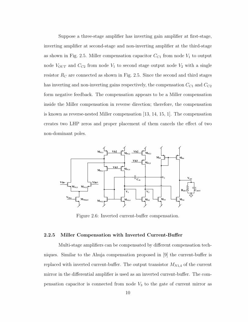
2.2.5 Miller Compensation with Inverted Current-Buffer
Multi-stage amplifiers can be compensated by different compensation tech-
niques. Similar to the Ahuja compensation proposed in [9] the current-buffer is
replaced with inverted current-buffer. The output transistor MN1,4 of the current
mirror in the differential amplifier is used as an inverted current-buffer. The com-
pensation capacitor is connected from node V3 to the gate of current mirror as
10

shown in Fig. 2.6. The input impedance of the inverted current-buffer is 1GM
and
this helps in creating LHP zeros. This also helps in improving the bandwidth and
wide driving capability.
2.3 Class AB Amplifiers
Class AB amplifiers have a wide range of applications in portable electronic
devices. They are used in the design of circuits such as audio amplifiers, motor
drivers and LED & LCD drivers [3]. Most of these applications require class AB
amplifiers with low power, high efficiency, and stability for a wide range of loads.
They are also required to have rail-to-rail operation when driving low resistive
loads. Class AB amplifiers can generate large output currents that are much
greater than the quiescent current of the output stage, thereby maintaining low
static power consumption [16]. As the power supply is decreasing the operating
speed and the dynamic range of analog amplifier is becoming more limited [17].
High slew rate is also an important factor for a class AB amplifiers used as LCD
drivers [18]. Achieving all of these performance requirements simultaneously is
becoming more complex for designers.
The class AB amplifier can deliver huge output current with very low
quiescent. The output current is not limited by the bias current and therefore has
very high efficiency. The pseudo-class AB amplifier can also deliver huge output
currents that are not limited by the bias current, but the quiescent current is
huge. The quiescent current is proportional to the output current and therefore
has a low current efficiency. A three-stage pseudo-class AB amplifier is described
in the next section.
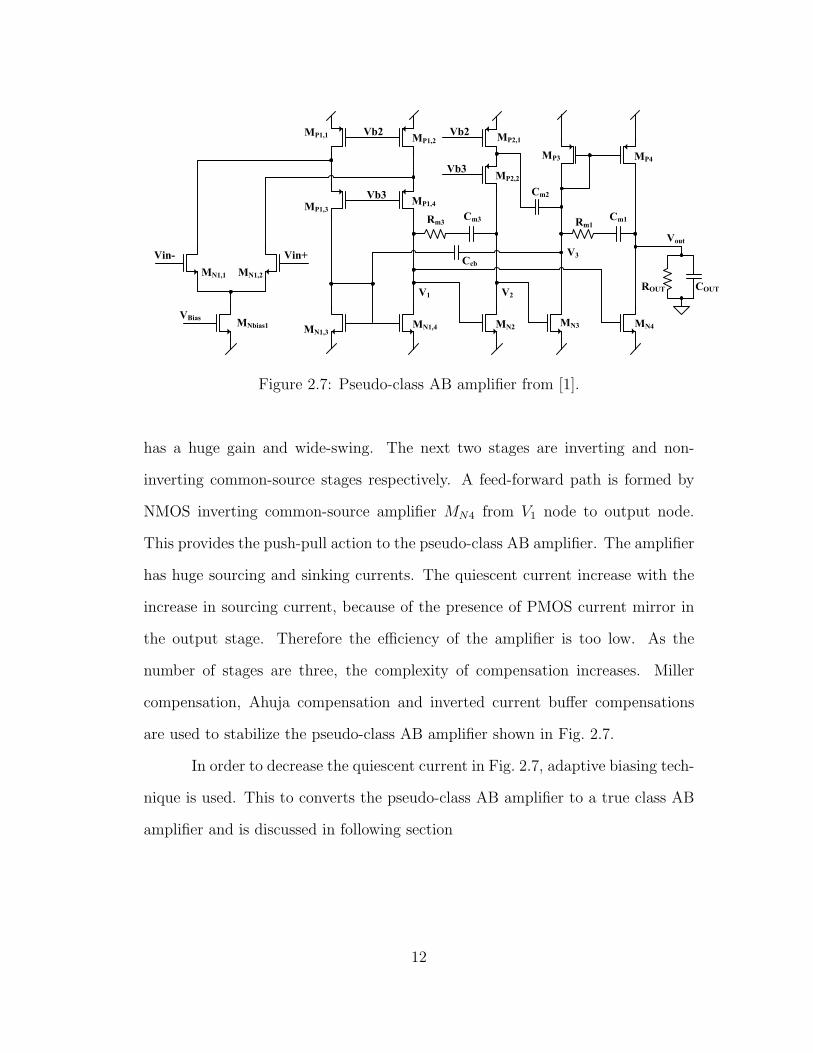
2.3.1 I-I-N Pseudo Class-AB Amplifier [1]
The pseudo-class AB amplifier shown in the Fig. 2.7 is three-stage amplifier
proposed in [1]. First-stage of the amplifier is a folded cascode amplifier, that
11
Vin+
VBias
Vb3
Vb2
Vin-
Vb2
Vb3
MNbias1MN1,3
MN2
MN1,1 MN1,2
MP1,3MP1,4
MP1,2
MP2,2
MP2,1
MN3
MP4
MN4
MP3
ROUT COUT
Ccb
V1 V2
V3
Vout
MN1,4
MP1,1
Rm3 Rm1Cm3 Cm1
Cm2
Figure 2.7: Pseudo-class AB amplifier from [1].
has a huge gain and wide-swing. The next two stages are inverting and non-
inverting common-source stages respectively. A feed-forward path is formed by
NMOS inverting common-source amplifier MN4 from V1 node to output node.
This provides the push-pull action to the pseudo-class AB amplifier. The amplifier
has huge sourcing and sinking currents. The quiescent current increase with the
increase in sourcing current, because of the presence of PMOS current mirror in
the output stage. Therefore the efficiency of the amplifier is too low. As the
number of stages are three, the complexity of compensation increases. Miller
compensation, Ahuja compensation and inverted current buffer compensations
are used to stabilize the pseudo-class AB amplifier shown in Fig. 2.7.
In order to decrease the quiescent current in Fig. 2.7, adaptive biasing tech-
nique is used. This to converts the pseudo-class AB amplifier to a true class AB
amplifier and is discussed in following section
12
Vin+
VBias
Vb3
Vb2
Vin-
Vb2
Vb3
MNbias1MN1,3
MN2
MN1,1 MN1,2
MP1,3MP1,4
MP1,2
MP2,2
MP2,1
MN3
MP4
MN4
MP3
ROUT COUT
Ccb
V1 V2
V3
Vout
MN1,4
MP1,1
Rm3 Rm1Cm3 Cm1
Cm2
Rad1
Rad2
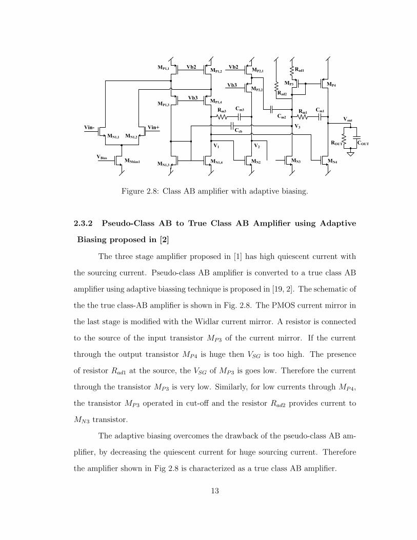
Figure 2.8: Class AB amplifier with adaptive biasing.
2.3.2 Pseudo-Class AB to True Class AB Amplifier using Adaptive
Biasing proposed in [2]
The three stage amplifier proposed in [1] has high quiescent current with
the sourcing current. Pseudo-class AB amplifier is converted to a true class AB
amplifier using adaptive biassing technique is proposed in [19, 2]. The schematic of
the the true class-AB amplifier is shown in Fig. 2.8. The PMOS current mirror in
the last stage is modified with the Widlar current mirror. A resistor is connected
to the source of the input transistor MP3 of the current mirror. If the current
through the output transistor MP4 is huge then VSG is too high. The presence
of resistor Rad1 at the source, the VSG of MP3 is goes low. Therefore the current
through the transistor MP3 is very low. Similarly, for low currents through MP4,
the transistor MP3 operated in cut-off and the resistor Rad2 provides current to
MN3 transistor.
The adaptive biasing overcomes the drawback of the pseudo-class AB am-
plifier, by decreasing the quiescent current for huge sourcing current. Therefore
the amplifier shown in Fig 2.8 is characterized as a true class AB amplifier.
13
In this project, we analysed two widely-used pseudo-class AB amplifiers
that has high-gain multi-stage amplifier with a simple biasing circuit, low transistor-
count and wide output-swing. The amplifier can operate with low supply voltages
and currents. Therefore, the amplifier is widely reported in [20, 21, 13, 22, 19, 2].
We improved the topology of the pseudo-class AB amplifiers and converted to a
true class AB amplifiers.
14

Chapter 3
DESIGN AND SIMULATIONS
Two different pseudo-class AB amplifiers are discussed in this section that are
converted to true class AB amplifiers. Both of these pseudo-class AB amplifiers
are three-stage. One amplifier has inverting, inverting and non-inverting (I-I-N)
cascade stages. The other amplifier has inverting, non-inverting and inverting
(I-N-I) cascade stages. Both the amplifiers are widely used because of high-gain,
low transistor-count, simple biasing circuit and wide output-swing. The amplifiers
can operate with low supply voltage, bias current and can generate huge output
currents.
3.1 I-I-N Three-stage Pseudo-Class AB Amplifier
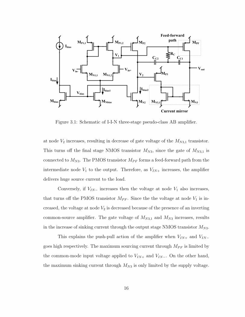
A three-stage pseudo-class AB amplifier shown in Fig. 3.1 is the NMOS
version of the circuit in [1]. The first stage is a differential amplifier and the next
two stages are common-source amplifiers. The first common-source amplifier has
negative gain and the second one has positive gain. The PMOS transistor MPF ,
which is an inverting common-source amplifier, creates a feed-forward path from
the intermediate node to the final output to produce the push-pull action for the
amplifier.
3.1.1 Operation
As the input VIN+ increases, the current through theMN1,2 increases results
in the decrement of voltage at node V1. Therefore the current through MP2 and
MPF increases. Since the transistor MN2 can sink only bias current, the voltage
15
MP1,1 MP1,2
MN1,1 MN1,2
MNbias
Vbias
Vin-Vin+
Vout
MP2
MN2
RC
MP3
MN3,1 MN3
MPF
CC2 CC1
Feed-forward
path
Current mirror
V1
V2
Ibias
Mbias
+
Ibias
Ibias1Ibias2
Figure 3.1: Schematic of I-I-N three-stage pseudo-class AB amplifier.
at node V2 increases, resulting in decrease of gate voltage of the MN3,1 transistor.
This turns off the final stage NMOS transistor MN3, since the gate of MN3,1 is
connected to MN3. The PMOS transistor MPF forms a feed-forward path from the
intermediate node V1 to the output. Therefore, as VIN+ increases, the amplifier
delivers huge source current to the load.
Conversely, if VIN− increases then the voltage at node V1 also increases,
that turns off the PMOS transistor MPF . Since the the voltage at node V1 is in-
creased, the voltage at node V2 is decreased because of the presence of an inverting
common-source amplifier. The gate voltage of MN3,1 and MN3 increases, results
in the increase of sinking current through the output stage NMOS transistor MN3.
This explains the push-pull action of the amplifier when VIN+ and VIN−
goes high respectively. The maximum sourcing current through MPF is limited by
the common-mode input voltage applied to VIN+ and VIN−. On the other hand,
the maximum sinking current through MN3 is only limited by the supply voltage.
16
The last stage of the amplifier is a non-inverting common source amplifier.
It comprises a NMOS current mirror formed by MN3,1 and MN3 with a dimension
ratio of in 1:K. Since MN3 is the output transistor it can pull a large sinking cur-
rent, that results in correspondingly large current through the mirrored transistor
MN3,1. Thus the quiescent current is increases with the increase in output sinking
current, resulting in the loss of current efficiency and power. Hence, the amplifier
is designated as a pseudo-class AB amplifier.
Table 3.1: Dimensions of transistors
I-I-N pseudo-class AB
MN1,1,MN1,2,MN2,MN3,1
101.2,m = 2
MP1,1,MP1,2,MP2301.2,m = 2
MN3 & MPF101.2
& 301.2,m = 8
MNbias1101.2,m = 4
MNbias101.2,m = 1
RC 6.5kΩ
CC1, CC2 7.5pF, 7.5pF
Reverse-nested Miller compensation with resistor is used to stabilize the
amplifier for a wide range of capacitive loads. The dimensions of all the transistors,
resistors and capacitors are given in Table 3.1.
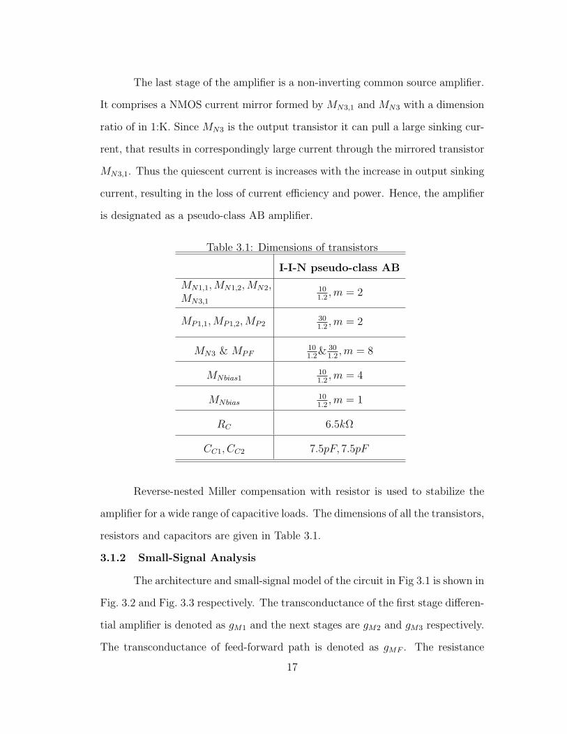
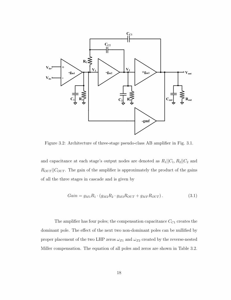
3.1.2 Small-Signal Analysis
The architecture and small-signal model of the circuit in Fig 3.1 is shown in
Fig. 3.2 and Fig. 3.3 respectively. The transconductance of the first stage differen-
tial amplifier is denoted as gM1 and the next stages are gM2 and gM3 respectively.
The transconductance of feed-forward path is denoted as gMF . The resistance
17
-gm1
Vin+
Vout
+
-
-gm2 +gm3
-gmf
CC1
CC2
R1C1 R2C2 RoutCout
Vin-
V1 V2
RC
Figure 3.2: Architecture of three-stage pseudo-class AB amplifier in Fig. 3.1.
and capacitance at each stage’s output nodes are denoted as R1||C1, R2||C2 and
ROUT ||COUT . The gain of the amplifier is approximately the product of the gains
of all the three stages in cascade and is given by
Gain = gM1R1 · (gM2R2 · gM3ROUT + gMFROUT ) . (3.1)
The amplifier has four poles; the compensation capacitance CC1 creates the
dominant pole. The effect of the next two non-dominant poles can be nullified by
proper placement of the two LHP zeros ωZ1 and ωZ2 created by the reverse-nested
Miller compensation. The equation of all poles and zeros are shown in Table 3.2.
18
CC1
R1C1
V1
gm1Vin
CC2
gm3fV1
Vin
G
+
–
RC
R2C2
V2
gm2V1 RoutCout
Vout
gm3V2
S
Figure 3.3: Small-signal model of three-stage pseudo-class AB amplifier in Fig. 3.1.
Table 3.2: Equations of Poles and Zeros of I-I-N Pseudo-Class AB Amplifier
Poles Zeros
ωP1 = 1gM2R2·gM3ROUT ·R1·CC1
ωP2 = gM3CC1
CC2·(CC1+COUT ) ωZ1 = 1RC ·(CC1+CC2)
ωP3 = gM3·(CC1+COUT )CC1·CCOUT
ωZ2 = gM2·gM3·(CC1+CC2)(gM2+gM3)·CC1·CC2
ωP4 = 1RC ·C1
The two non-dominant pole locations discussed above are dependent on the
output capacitor and the zeros are dependent on the compensation capacitor val-
ues. If the output capacitor is comparable to the compensation capacitor values,
then the zeros can cancel the effect of poles. If the value of output capacitor is too
large, then the poles move to low frequencies and the value of the compensation
capacitor that cancel the poles may become prohibitively large. If cancelling is
not possible, then phase margin and gain margin may decrease. Therefore the
stability of the amplifier for wide range of capacitive loads with small values of
compensation is limited. From simulation and experimental results, the amplifier
19
is stable for maximum load of 200pF with a total of 15pF compensation capaci-
tance.
The last pole ωP4 is high frequency pole located far beyond the unity gain
frequency and the effect of this pole on stability is assumed to be negligible.
To convert the pseudo-class AB amplifier shown in Fig. 3.1 to a class AB
amplifier, the first step is to avoid current mirrors at the output stage. In order to
avoid the current mirror at the output stage, a I-N-I three-stage pseudo class AB
amplifier is designed and described in next section.
3.2 I-N-I Three-stage Pseudo-Class AB Amplifier
MP1,1 MP1,2
MN1,1 MN1,2
MNbias1
Vbn
Vin- Vin+
Vout
MP2,1
MN2,1
RC
MP2,2
MN2,2 MN3
MPF
CC2
CC1
MNbias
MPbias
Vbp
Vbp
Ibias
V1
V2
Figure 3.4: Schematic of I-N-I three-stage pseudo-class AB amplifier.
The schematic of I-N-I three-stage pseudo-class AB amplifier shown in
Fig. 3.4. The first stage is a differential amplifier and the next two stages are
common-source amplifiers. The first common-source amplifier has positive gain
and the second one has negative gain. The PMOS transistor MPF , which is an
inverting common-source amplifier, creates a feed-forward path from the interme-
diate node V1 to the final output to produce the push-pull action for the amplifier.
Nested Miller compensation with resistor is used to stabilize the amplifier for a
20
wide range of capacitive loads. The dimensions of all the transistors, resistors and
capacitors are given in Table 3.3.
3.2.1 Operation
As the input VIN+ increases the current through the MN1,2 increases results
in the decrement of voltage at node V1. Therefore the current through MP2 and
MPF increases. Since the node V1 is connected to the second stage, which is a
non-inverting common-source amplifier and the transistor MP2,2 can source only
bias current, the voltage at node V2 also decreases. This turns off the final stage
NMOS transistor MN3. The PMOS transistor MPF forms a feed-forward path
from the intermediate node V1 to the output. Therefore the amplifier delivers
huge source current if VIN+ increases.
Conversely, if VIN− increases then the voltage at node V1 also increases,
turning off PMOS transistor MPF . Since the the voltage at node V1 is in-
creased, the voltage at node V2 increases because of the presence of a non-inverting
common-source amplifier. This results in the increase of current through the out-
put stage NMOS transistor MN3. Therefore the amplifier has a huge sinking
current if VIN− increases.
This explains the push-pull action of the amplifier when VIN+ and VIN−
increases respectively. The maximum sourcing current through MPF is limited by
the common-mode input voltage applied to VIN+ and VIN−. On the other hand,
the maximum sinking current through MN3 is only limited by the supply voltage.
The second stage of the amplifier is a non-inverting common source ampli-
fier. It comprises a NMOS current mirror formed by MN2,1 and MN2,2 with same
dimensions. Since the first and second stages of the amplifier shown in Fig. 3.4
is biased with the bias current, the quiescent current seems to be nearly constant
21
-gm1
Vin+Vout
+
-
gm2 -gm3
-gmF
CC1
R1C1 R2C2 RoutCout
Vin-
V1 V2
RC
CC2
Figure 3.5: Architecture of three-stage pseudo-class AB amplifier in Fig. 3.4.
Table 3.3: Dimensions of transistors
I-N-I pseudo-class AB
MN1,1,MN1,2,MN2,1,MN2,2
101.2,m = 2
MP1,1,MP1,2,MP2,1,MP2,2
301.2,m = 2
MN3 & MPF101.2
& 301.2,m = 8
MNbias1101.2,m = 4
MNbias,MPbias101.2, 30
1.2,m = 1
RC 3kΩ
CC1, CC2 7.25pF, 7.25pF
22
irrespective of the output stage current. But the analysis shows that the amplifier
is pseudo-class AB amplifier.
When the sourcing current increases then the voltage at node V1 decreases.
The current through the PMOS transistor MP2,1 also increases. Since, the NMOS
transistor MN2,1 is not limited to bias current, the current through that branch is
also increases. The increment in current also mirrors toMN2,2 transistor because of
the current mirror formed by MN2,1 and MN2,2. Since the current through PMOS
transistor MP2,2 is limited to bias current, the voltage at node V2 decreases and
turns off output NMOS transistor. Thus the quiescent current is increased when
the output is sourcing, resulting in the loss of current efficiency and power; hence,
the designation pseudo-class AB amplifier.
CC1
R1C1
V1
gm1Vin gm3fV1
Vin
G
+
–
R2C2
V2
gm2V1 RoutCout
Vout
gm3V2
S
CC2 RC
Figure 3.6: Small-signal model of three-stage pseudo-class AB amplifier in Fig. 3.4.
3.2.2 Small-Signal Analysis
The architecture and small-signal model of the circuit in Fig 3.4 is shown in
Fig. 3.5 and Fig. 3.6 respectively. The transconductance of the first stage differen-
tial amplifier is denoted as gM1 and the next stages are gM2 and gM3 respectively.
The transconductance of feed-forward path is denoted as gMF . The resistance
and capacitance at each stage’s output nodes are denoted as R1||C1, R2||C2 and
ROUT ||COUT . The gain of the amplifier is approximately the product of the gains
23

of all the three stages in cascade and is given by
Gain = gM1R1 · (gM2R2 · gM3ROUT + gM3ROUT ) . (3.2)
The amplifier has four poles; the compensation capacitance CC1 creates the dom-
inant pole. The effect of the next two non-dominant poles ωP2 and ωP3 can be
nullified by proper placement of the two LHP zeros ωZ1 and ωZ2 created by the
reverse-nested Miller compensation. The equation of all poles and zeros are men-
tioned in Table 3.4.
Table 3.4: Equations of Poles and Zeros of I-N-I Pseudo-Class AB Amplifier
Poles Zeros
ωP1 = 1gM2R2·gM3ROUT ·R1·CC1
ωP2 = gM2·gM3
CC2(gM3+gMF−gM2(1+ RCROUT
))ωZ1 = 1
RC ·(CC1+CC2)
ωP3 =CC2(gM3+gMF−gM2(1+ RC
ROUT))
gM2·RC ·COUTωZ2 = gM2·gM3·(CC1+CC2)
(gMF +gM3)·CC1·CC2
ωP4 = 1RC ·C1
The two non-dominant pole locations discussed above are dependent on
the output resistor and the zeros are dependent on the compensation capacitor
values. If the ROUT is less than RC , then the second and third LHP poles change
to RHP poles creating oscillations in the amplifier. Therefore the value of the
compensation resistor should be less than ROUT and the amplifier is not stable
for low values of output resistance. If the value of output resistor is close to value
of compensation resistor RC , then the second pole moves to infinity. The third
pole moves towards zero and the two LHP zeros helps in stabilizing the amplifier.
24

If the ROUT is much greater than the RC , then the second and third pole are the
two non-dominant poles that are cancelled by the proper placement of two zeros.
The last pole ωP4 is high frequency pole located far beyond the unity gain
frequency and the effect of this pole on stability is assumed to be negligible.
The stability and bandwidth of pseudo-class AB amplifiers are limited by
the values of load capacitor or resistor. A novel compensation technique for multi-
stage amplifiers is presented in the next section for improving stability, bandwidth
and PSRR.
3.3 Inverted Current-Buffer Compensation
The inverted current buffer compensation technique is used in I-I-N pseudo-
class AB amplifiers discussed earlier. The proposed compensation has a capacitor
from the output node to the bias node and the bias transistor of second stage MN2
acts as an inverted current buffer. The three stage amplifier shown in Fig. 3.1
is already compensated with reverse-nested Miller compensation. The proposed
compensation technique is applied to the amplifier with a capacitor CCB from
output node to the bias node VBIAS and is shown in Fig. 3.7.
The addition of proposed compensation reduces the capacitor values used
in reverse nested Miller compensation to stabilize the amplifier. This results in
increased bandwidth and PSRR. The dimensions of all the transistors, capacitors
and resistors are mentioned in Table. 3.5.
3.3.1 Inverted Current Buffer
The amplifier has three bias transistors, one is the diode connected transis-
tor Mbias, that supplies bias currents to the rest of the circuit through VBias node.
The second one is the tail transistor MNbias1 of differential amplifier and the other
one MN2 that acts as a current source for the second stage common-source am-
plifier. The compensation capacitor CCB from output node is connected to VBias
25
MP1,1 MP1,2
MN1,1 MN1,2
MNbias1
Vbias
Vin- Vin+ Vout
MP2
MN2
RC
MP3
MN3,1 MN3
MP3,F
CC2 CC1
CCBIbias
Mbias
+
Ibias
Ibias1 Ibias2
Figure 3.7: Schematic of three-stage pseudo-class AB amplifier with inverted cur-rent buffer compensation.
Table 3.5: Dimensions of transistors
I-I-N pseudo-class AB with CCB
MN1,1,MN1,2,MN2,MN3,1
101.2,m = 2
MP1,1,MP1,2,MP2301.2,m = 2
MN3 & MPF101.2
& 301.2,m = 8
MNbias1101.2,m = 4
MNbias101.2, 30
1.2,m = 1
RC 8kΩ
CC1, CC2, CCB 3pF
node. Since the bias transistor MNbias1 is the tail transistor for the differential
amplifier, the compensation has almost no effect on it. Though the compensation
induces any feedback current into the tail transistor MNbias1, the current mirror
inside the differential amplifier cancels the effect of it.
26
-gm1
Vin+
Vout
+
-
-gm2 +gm3
-gm4f
CC1
CC2
R1C1 R2C2 RoutCout
Vin-
V1 V2
RC
-gmfb
CCb
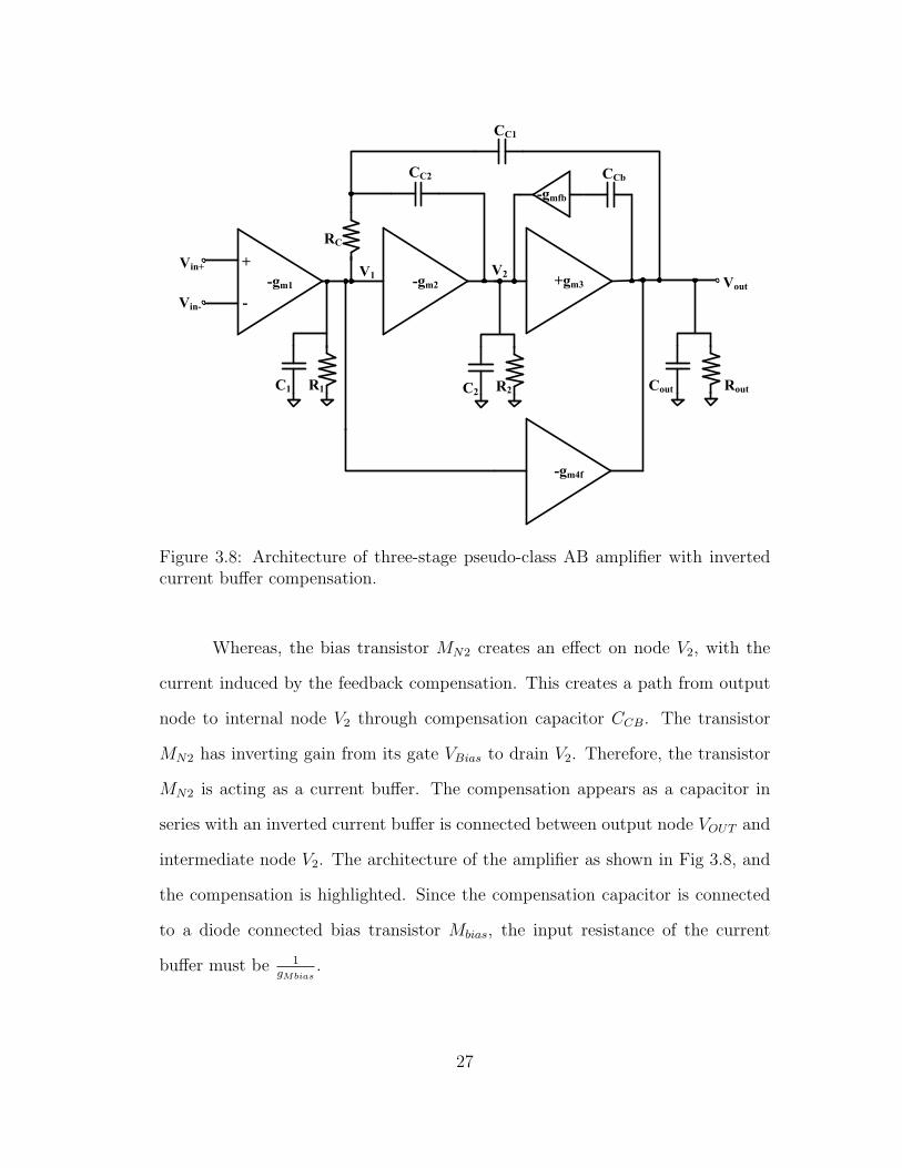
Figure 3.8: Architecture of three-stage pseudo-class AB amplifier with invertedcurrent buffer compensation.
Whereas, the bias transistor MN2 creates an effect on node V2, with the
current induced by the feedback compensation. This creates a path from output
node to internal node V2 through compensation capacitor CCB. The transistor
MN2 has inverting gain from its gate VBias to drain V2. Therefore, the transistor
MN2 is acting as a current buffer. The compensation appears as a capacitor in
series with an inverted current buffer is connected between output node VOUT and
intermediate node V2. The architecture of the amplifier as shown in Fig 3.8, and
the compensation is highlighted. Since the compensation capacitor is connected
to a diode connected bias transistor Mbias, the input resistance of the current
buffer must be 1gMbias
.
27
3.3.2 Small-Signal Model
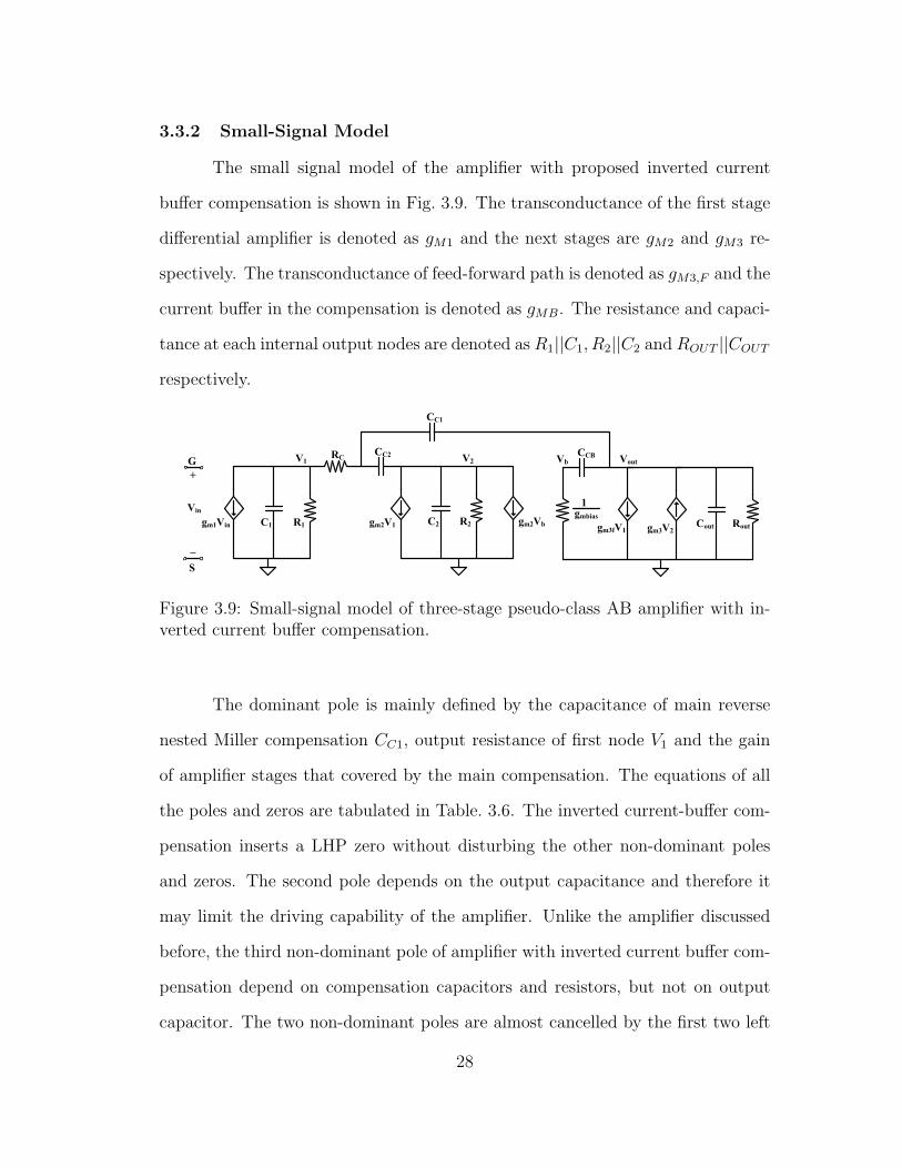
The small signal model of the amplifier with proposed inverted current
buffer compensation is shown in Fig. 3.9. The transconductance of the first stage
differential amplifier is denoted as gM1 and the next stages are gM2 and gM3 re-
spectively. The transconductance of feed-forward path is denoted as gM3,F and the
current buffer in the compensation is denoted as gMB. The resistance and capaci-
tance at each internal output nodes are denoted as R1||C1, R2||C2 and ROUT ||COUT
respectively.
CC1
R1C1
V1
gm1Vin
CC2
gm3fV1
Vin
G
+
–
RC
R2C2
V2
gm2V1 RoutCout
Vout
gm3V2
S
Vb
CCB
gmbias
1
gm2Vb
Figure 3.9: Small-signal model of three-stage pseudo-class AB amplifier with in-verted current buffer compensation.
The dominant pole is mainly defined by the capacitance of main reverse
nested Miller compensation CC1, output resistance of first node V1 and the gain
of amplifier stages that covered by the main compensation. The equations of all
the poles and zeros are tabulated in Table. 3.6. The inverted current-buffer com-
pensation inserts a LHP zero without disturbing the other non-dominant poles
and zeros. The second pole depends on the output capacitance and therefore it
may limit the driving capability of the amplifier. Unlike the amplifier discussed
before, the third non-dominant pole of amplifier with inverted current buffer com-
pensation depend on compensation capacitors and resistors, but not on output
capacitor. The two non-dominant poles are almost cancelled by the first two left
28
half plane (LHP) zeros created by the compensation. Therefore the amplifier is
approximated as a two poles and one zero system. The LHP zero may be located
just before or after high frequency non-dominant LHP pole depending on value of
output capacitor. Though the second pole is dependent on the output capacitor,
the three LHP zeros make the amplifier stable for a wide range of capacitive loads.
The last pole is located at very high frequencies beyond the unity gain frequency,
therefore the effect if it is neglected.
Table 3.6: Equations of Poles and Zeros of Amplifier with Inverted Current BufferCompensation
Poles Zeros
ωP1 = 1gM2R2·gM3ROUT ·R1·CC1
ωP2 = gM2CC1
CC2COUTωZ1 = 1
RC(CC1+CC2)
ωP3 = gM2
CC2ωZ2 = gM2gM3(CC1+CC2)
(gM2+gMF )CC1CC2
ωP4 = R1(gM2CCB+gMbiasCC1)CCB ·CC1(R1+RC) ωZ3 = gMbias
CCB
3.4 Simulation Results Compared with Inverted Current-Buffer Com-
pensation
All the pseudo-class AB amplifiers and pseudo-class AB amplifier with
inverted current-buffer compensation is designed and simulated in AMI 0.5µm
process. The DC, AC and transient simulations are done and the outputs are
shown in the next subsections. The results of I-I-N pseudo-class AB amplifier
with inverted current-buffer compensation is compared with the results of I-I-N
and I-N-I pseudo-class AB amplifier without inverted current-buffer compensation
and the results are summarized in Table. 3.7.
29

+
Vout
+
-
RLCL
VSIN
+
-
Amplifier
RLargeCLarge
AC magnitude =1
Phase = -180
Figure 3.10: AC analysis test bench of three-stage pseudo-class AB amplifierswithout and with inverting current-buffer compensation.
Figure 3.11: Frequency plot of I-I-N three-stage pseudo-class AB amplifier.
30
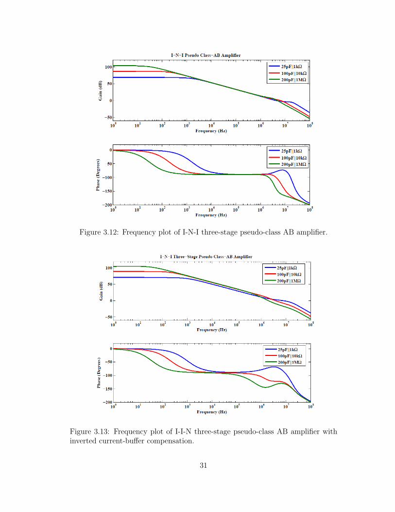
Figure 3.12: Frequency plot of I-N-I three-stage pseudo-class AB amplifier.
Figure 3.13: Frequency plot of I-I-N three-stage pseudo-class AB amplifier withinverted current-buffer compensation.
31
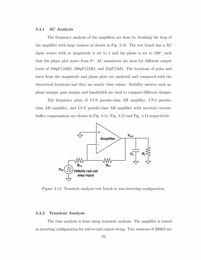
3.4.1 AC Analysis
The frequency analysis of the amplifiers are done by breaking the loop of
the amplifier with large resistor as shown in Fig. 3.10. The test bench has a AC
input source with ac magnitude is set to 1 and the phase is set to 180o, such
that the phase plot starts from 0o. AC simulation are done for different output
loads of 100pF||10kΩ, 200pF||1MΩ, and 25pF||1kΩ. The locations of poles and
zeros from the magnitude and phase plots are analysed and compared with the
theoretical locations and they are nearly close values. Stability metrics such as,
phase margin, gain margin and bandwidth are used to compare different designs.
The frequency plots of I-I-N pseudo-class AB amplifier, I-N-I pseudo-
class AB amplifier, and I-I-N pseudo-class AB amplifier with inverted current-
buffer compensation are shown in Fig. 3.11, Fig. 3.12 and Fig. 3.13 respectively.
Vout
+
-
RLCL
VIN
+
-
Amplifier
RF1RF2
+
100kHz rail-rail
step input
Figure 3.14: Transient analysis test bench in non-inverting configuration.
3.4.2 Transient Analysis
The time analysis is done using transient analysis. The amplifier is tested
as inverting configuration for rail-to-rail output swing. Two resistors of 200kΩ are
32
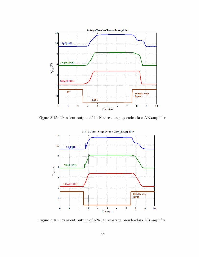
Figure 3.15: Transient output of I-I-N three-stage pseudo-class AB amplifier.
Figure 3.16: Transient output of I-N-I three-stage pseudo-class AB amplifier.
33
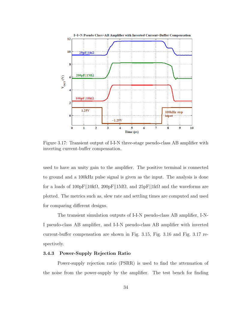
Figure 3.17: Transient output of I-I-N three-stage pseudo-class AB amplifier withinverting current-buffer compensation.
used to have an unity gain to the amplifier. The positive terminal is connected
to ground and a 100kHz pulse signal is given as the input. The analysis is done
for a loads of 100pF||10kΩ, 200pF||1MΩ, and 25pF||1kΩ and the waveforms are
plotted. The metrics such as, slew rate and settling times are computed and used
for comparing different designs.
The transient simulation outputs of I-I-N pseudo-class AB amplifier, I-N-
I pseudo-class AB amplifier, and I-I-N pseudo-class AB amplifier with inverted
current-buffer compensation are shown in Fig. 3.15, Fig. 3.16 and Fig. 3.17 re-
spectively.
3.4.3 Power-Supply Rejection Ratio
Power-supply rejection ratio (PSRR) is used to find the attenuation of
the noise from the power-supply by the amplifier. The test bench for finding
34
Vout
+
-
RLCL
VIN
+
+
-
Amplifier
RF1RF2
+
VSIN
+
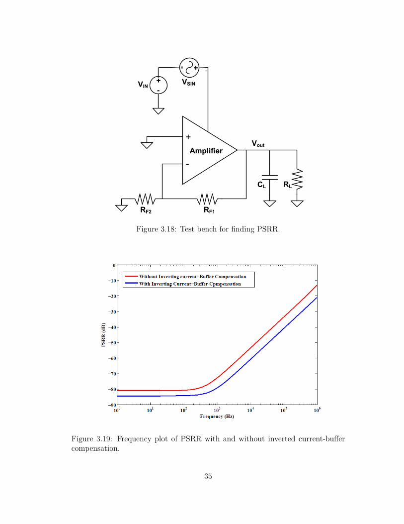
-Figure 3.18: Test bench for finding PSRR.
Figure 3.19: Frequency plot of PSRR with and without inverted current-buffercompensation.
35
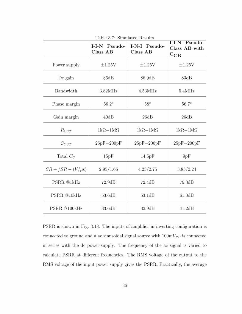
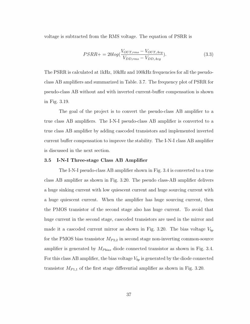
Table 3.7: Simulated Results
I-I-N Pseudo-Class AB
I-N-I Pseudo-Class AB
I-I-N Pseudo-Class AB withCCB
Power supply ±1.25V ±1.25V ±1.25V
Dc gain 86dB 86.9dB 83dB
Bandwidth 3.82MHz 4.53MHz 5.4MHz
Phase margin 56.2o 58o 56.7o
Gain margin 40dB 26dB 26dB
ROUT 1kΩ−1MΩ 1kΩ−1MΩ 1kΩ−1MΩ
COUT 25pF−200pF 25pF−200pF 25pF−200pF
Total CC 15pF 14.5pF 9pF
SR + /SR− (V/µs) 2.95/1.66 4.25/2.75 3.85/2.24
PSRR @1kHz 72.9dB 72.4dB 79.3dB
PSRR @10kHz 53.6dB 53.1dB 61.0dB
PSRR @100kHz 33.6dB 32.9dB 41.2dB
PSRR is shown in Fig. 3.18. The inputs of amplifier in inverting configuration is
connected to ground and a ac sinusoidal signal source with 100mVPP is connected
in series with the dc power-supply. The frequency of the ac signal is varied to
calculate PSRR at different frequencies. The RMS voltage of the output to the
RMS voltage of the input power supply gives the PSRR. Practically, the average
36
voltage is subtracted from the RMS voltage. The equation of PSRR is
PSRR+ = 20log(VOUT,rms − VOUT,Avg
VDD,rms − VDD,Avg
). (3.3)
The PSRR is calculated at 1kHz, 10kHz and 100kHz frequencies for all the pseudo-
class AB amplifiers and summarized in Table. 3.7. The frequency plot of PSRR for
pseudo-class AB without and with inverted current-buffer compensation is shown
in Fig. 3.19.
The goal of the project is to convert the pseudo-class AB amplifier to a
true class AB amplifiers. The I-N-I pseudo-class AB amplifier is converted to a
true class AB amplifier by adding cascoded transistors and implemented inverted
current buffer compensation to improve the stability. The I-N-I class AB amplifier
is discussed in the next section.
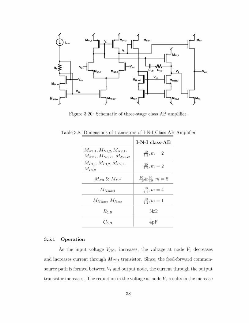
3.5 I-N-I Three-stage Class AB Amplifier
The I-N-I pseudo-class AB amplifier shown in Fig. 3.4 is converted to a true
class AB amplifier as shown in Fig. 3.20. The pseudo class-AB amplifier delivers
a huge sinking current with low quiescent current and huge sourcing current with
a huge quiescent current. When the amplifier has huge sourcing current, then
the PMOS transistor of the second stage also has huge current. To avoid that
huge current in the second stage, cascoded transistors are used in the mirror and
made it a cascoded current mirror as shown in Fig. 3.20. The bias voltage Vbp
for the PMOS bias transistor MP2,2 in second stage non-inverting common-source
amplifier is generated by MPbias diode connected transistor as shown in Fig. 3.4.
For this class AB amplifier, the bias voltage Vbp is generated by the diode connected
transistor MP1,1 of the first stage differential amplifier as shown in Fig. 3.20.
37
MP1,1 MP1,2
MN1,1 MN1,2
MNbias1
Vbn
Vin- Vin+
Vout
MP2,1
MN2,1
MP2,2
MN2,2 MN3
MPF
MNbias
MNcas
Ibias
MNcas1 MNcas2
VcnVcn
V1
V2
Vx
RCBCCBRB
Figure 3.20: Schematic of three-stage class AB amplifier.
Table 3.8: Dimensions of transistors of I-N-I Class AB Amplifier
I-N-I class-AB
MN1,1,MN1,2,MN2,1,MN2,2,MNcas1,MNcas2
101.2,m = 2
MP1,1,MP1,2,MP2,1,MP2,2
301.2,m = 2
MN3 & MPF101.2
& 301.2,m = 8
MNbias1101.2,m = 4
MNbias, MNcas101.2,m = 1
RCB 5kΩ
CCB 4pF
3.5.1 Operation
As the input voltage VIN+ increases, the voltage at node V1 decreases
and increases current through MP2,1 transistor. Since, the feed-forward common-
source path is formed between V1 and output node, the current through the output
transistor increases. The reduction in the voltage at node V1 results in the increase
38
the current through MP2,1. In the pseudo-class AB amplifier shown in Fig. 3.4,
the current through the second stage is not limited to the bias current. But in this
class AB amplifier, the current is limited by the cascoded transistor MNCAS1 and
therefore the voltage at the gate of current mirror increases and in turn decreases
the voltage at node V2. This turns off the output NMOS transistor MN3. Since
all the internal stage currents of the amplifier are limited by the bias current, the
quiescent current is very low when there is a huge sourcing current.
As the input voltage VIN− increases, the voltage at node V1 also increases.
This turns off the PMOS transistor MP2,1 and the feed-forward PMOS transistor
MPF . As the voltage at node V1 increases, the voltage at node V2 also increases.
This increases the sinking current through the output NMOS transistor MN4.
Similar to the pseudo-class AB amplifier shown in Fig. 3.4, all the internal stage
currents of the amplifier are limited by the bias current, the quiescent current is
very low when there is a huge sinking current.
This explains the push-pull action of the amplifier when VIN+ and VIN−
increases respectively. The maximum sourcing current through MPF is limited by
the common-mode input voltage applied to VIN+ and VIN−. On the other hand,
the maximum sinking current through MN3 is only limited by the supply voltage.
This confirms the true class AB characterization of I-N-I three-stage class AB
amplifier.
3.5.2 Nested Inverted Current-Buffer Compensation
The I-N-I pseudo-class AB amplifier is compensated with nested Miller
compensation and is stable for wide range of capacitive and resistive loads. The
class AB amplifier shown in Fig. 3.20 is compensated with the inverted current-
buffer compensation and nested-miller compensation. The inverted current-buffer
compensation CCB and RCB is connected from node V2 to the gate of the current
39
-gm1
Vin+Vout
+
-
gm2 -gm3
-gmF
R1C1 R2C2 RoutCout
Vin-
V1 V2
RCB
CCB
-gm2x
-gm1x
gm1x1
Figure 3.21: Architecture of three-stage class AB amplifier.
mirror in the first stage differential amplifier. This help in forming two inverted
current-buffers, one is formed by MP1,2 transistor and the other is formed by
MP2,2 transistor. Therefore the compensation looks like a capacitor in series with
resistor and current-buffer in series to the node V1 and a current-buffer to node
V2. It is clearly observed in the architecture of class AB amplifier as shown
in Fig. 3.21. Therefore the compensation is called as nested inverted current-
buffer compensation. This increases the stability and bandwidth of the class AB
amplifier.
3.5.3 Small-Signal Analysis
The small signal model of the I-N-I class AB amplifier with inverted current
buffer compensation is shown in Fig. 3.22. The transconductance of the first
stage differential amplifier is denoted as gM1 and the next stages are gM2 and
40
CCB
R1C1
V1
gm1Vin gm3fV1
Vin
G
+
–
R2C2
V2
gm2V1 RoutCout
Vout
gm3V2
S
RCB
Vx
gm2xVxgm1xVxgm1x
1
Figure 3.22: Small-signal model of three-stage class AB amplifier.
gM3 respectively. The transconductance of feed-forward path is denoted as gMF
and the current buffer in the compensation is denoted as gMx. The resistance
and capacitance at each internal output nodes are denoted as R1||C1, R2||C2 and
ROUT ||COUT respectively. The gain of the amplifier is same as the discussed
amplifier given by
Gain = gM1R1 · (gM2R2 · gM3ROUT + gMFROUT ) . (3.4)
The amplifier has four poles; the compensation capacitance CCB creates the dom-
inant pole. The effect of the non-dominant pole can be nullified by proper place-
ment of the LHP zero ωZ1 created by the inverted current-buffer compensation.
The equation of all poles and zeros are mentioned in Table 3.9. The equation
of second pole is dependent on output resistor and capacitor. If the output ca-
pacitor is too small, then the second pole moves to higher frequencies. If the
capacitor is moderate, then the effect of pole is nullified by proper placement
of LHP zero. Therefore, the class AB amplifier is stable for low and moderate
output capacitance values. If the capacitor is too large, then the poles moves to
lower frequencies and effects the stability, phase margin and gain margin of the
amplifier.
41
Table 3.9: Equations of Poles and Zeros of I-N-I Class AB Amplifier
Poles Zeros
ωP1 = 1gM2R2·R1·CCB
ωP2 = 1ROUT COUT
ωZ1 = 1RCB ·CCB
ωP3 = gM2
C1ωZ2 = gM2·gM3
gMF ·C2
ωP4 = 1RCB ·C2
Similar to the output capacitance, the range of output resistance also effects
the movement of poles and zeros. If the output resistance ROUT is too small, then
the second pole moves to higher frequencies. If ROUT is moderate then the second
pole moves to moderate frequency and its effect is cancelled by proper placement
of LHP zero. If ROUT is too huge, then the second pole moves to lower frequencies
and effects the stability of the amplifier.
The combination of output capacitance and resistance effects the stability
of the class AB amplifier. For large output capacitance values, the amplifier is
stable for with low output resistor values. For small output capacitor, the amplifier
is stable for high output resistor.
The last two poles and last zero are at very high frequencies. The last pole
can be cancelled by proper placement of the lase zero. Therefore, the effect of
that pole and zero has almost no effect on the stability of the amplifier. The I-N-
I class AB amplifier overcomes the drawback of the pseudo-class AB amplifiers.
But, the class AB amplifier has slightly higher quiescent current with sourcing
current than the quiescent current with sinking current. This is because of the
presence of cascoded current mirror that has four times the bias current through
42

output transistor when the gate voltage goes close to negative rail voltage. This
drawback is overcome by the proposed class AB amplifier discussed in next section.
3.6 Proposed Three-stage True Class AB Amplifier
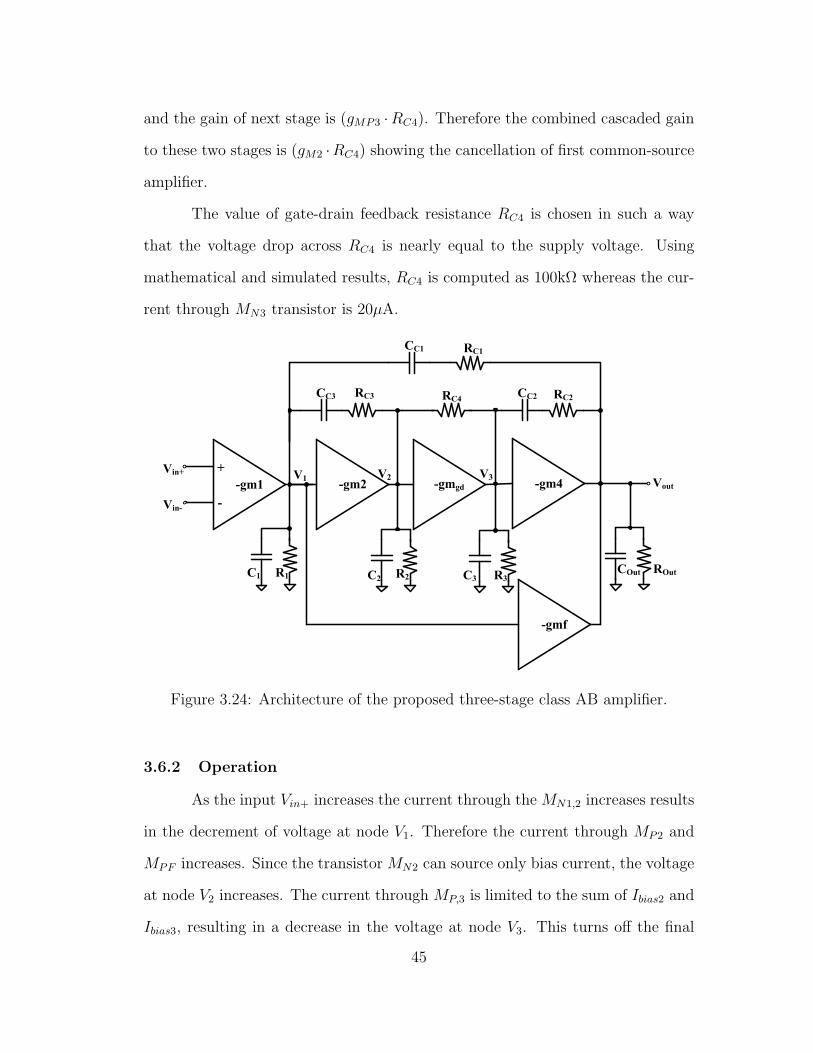
The schematic of the proposed three-stage class AB amplifier is shown in
Fig. 3.23. The first stage is a differential amplifier. Inverting common-source am-
plifiers make up the next stages. The first two inverting common-source amplifiers
MP2/MN2 and MP3/MN3 are combined with gate-drain feedback to behave as a
single non-inverting common-source stage. The output stage is formed by the
inverting common-source amplifiers MN4 and MPF . The common-source ampli-
fier MPF is the feed-forward path from V1 node to the output node. All internal
transistors have low quiescent current whereas the output stage has huge sourcing
and sinking current capability. This confirms the true class AB operation of the
output stage.
MP1,1 MP1,2
MN1,1 MN1,2
MNbias
Vbias
Vin-Vin+
Vout
MP2
MN2
RC3 CC3MP3
MN3 MN4
MPF
RC4
RC1
RC2
CC1
CC2
Feed-forward
path
Gate-drain
Feedback
V1
V2
V3
Ibias1 Ibias2 Ibias3
Ibias
Mbias
+
Ibias
Figure 3.23: Schematic of proposed three-stage class AB amplifier.
The proposed class AB amplifier employs both nested Miller compensa-
tion and reverse-nested Miller compensation techniques for stability. The main
compensation network CC1 and RC1 with CC2 and RC2 forms the nested Miller
43
compensation and CC1 and RC1 with CC3 and RC3 forms the reverse-nested Miller
compensation network. The dimensions of all transistors, capacitors and resistors
are given in Table 3.10. The nested and reverse nested Miller compensation in-
cluding the gate-drain feedback resistance helps in stabilizing the amplifier for a
wide range of capacitive and resistive loads.
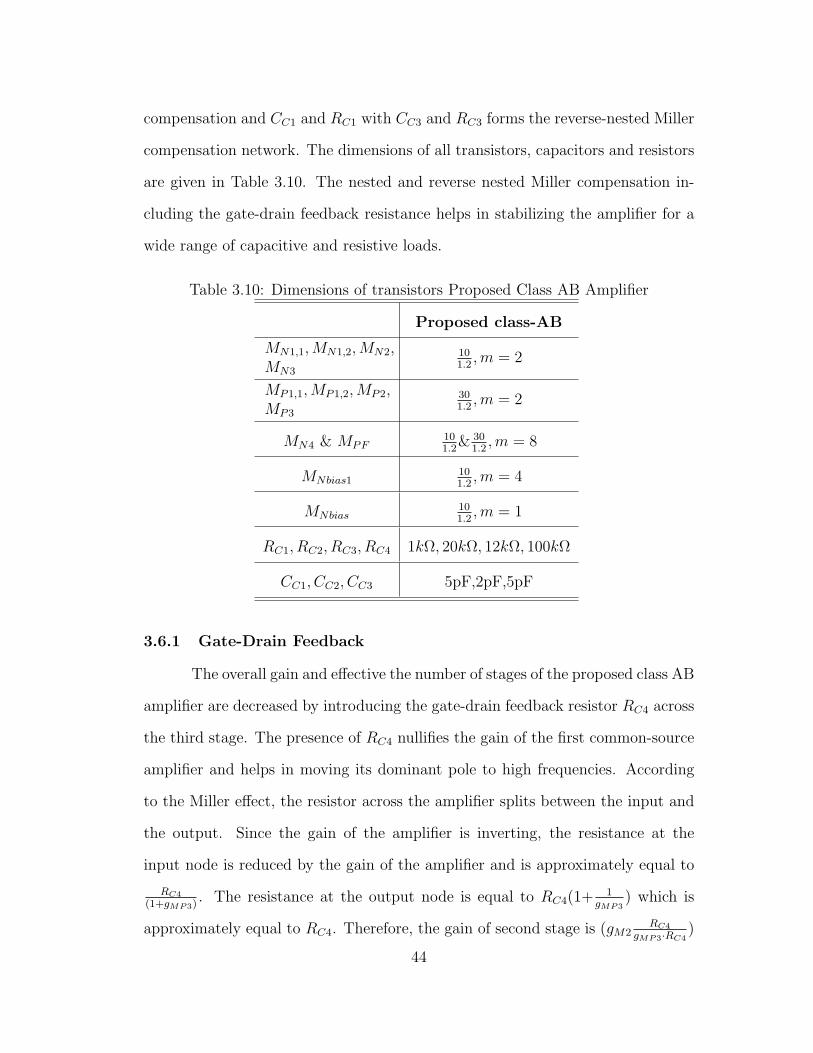
Table 3.10: Dimensions of transistors Proposed Class AB Amplifier
Proposed class-AB
MN1,1,MN1,2,MN2,MN3
101.2,m = 2
MP1,1,MP1,2,MP2,MP3
301.2,m = 2
MN4 & MPF101.2
& 301.2,m = 8
MNbias1101.2,m = 4
MNbias101.2,m = 1
RC1, RC2, RC3, RC4 1kΩ, 20kΩ, 12kΩ, 100kΩ
CC1, CC2, CC3 5pF,2pF,5pF
3.6.1 Gate-Drain Feedback
The overall gain and effective the number of stages of the proposed class AB
amplifier are decreased by introducing the gate-drain feedback resistor RC4 across
the third stage. The presence of RC4 nullifies the gain of the first common-source
amplifier and helps in moving its dominant pole to high frequencies. According
to the Miller effect, the resistor across the amplifier splits between the input and
the output. Since the gain of the amplifier is inverting, the resistance at the
input node is reduced by the gain of the amplifier and is approximately equal to
RC4
(1+gMP3). The resistance at the output node is equal to RC4(1+ 1
gMP3) which is
approximately equal to RC4. Therefore, the gain of second stage is (gM2RC4
gMP3·RC4)
44
and the gain of next stage is (gMP3 ·RC4). Therefore the combined cascaded gain
to these two stages is (gM2 ·RC4) showing the cancellation of first common-source
amplifier.
The value of gate-drain feedback resistance RC4 is chosen in such a way
that the voltage drop across RC4 is nearly equal to the supply voltage. Using
mathematical and simulated results, RC4 is computed as 100kΩ whereas the cur-
rent through MN3 transistor is 20µA.
-gm1
Vin+Vout
+
-
-gm2 -gmgd -gm4
-gmf
RC1CC1
RC4CC3 CC2RC3 RC2
R1C1 R2C2 R3C3ROutCOut
Vin-
V1 V2 V3
Figure 3.24: Architecture of the proposed three-stage class AB amplifier.
3.6.2 Operation
As the input Vin+ increases the current through the MN1,2 increases results
in the decrement of voltage at node V1. Therefore the current through MP2 and
MPF increases. Since the transistor MN2 can source only bias current, the voltage
at node V2 increases. The current through MP,3 is limited to the sum of Ibias2 and
Ibias3, resulting in a decrease in the voltage at node V3. This turns off the final
45
stage NMOS transistor MN4. The PMOS transistor MPF forms a feed-forward
path from the intermediate node V1 to the output. Therefore the amplifier delivers
source current if VIN+ increases.
Conversely, if VIN− increases then the current sinking through the NMOS
transistor MN4 increases. In this case the voltage at node V1 increases, turning off
PMOS transistor MPF . This explains the push-pull action of the amplifier. The
maximum sourcing current through MPF is limited by the common-mode input
voltage applied to VIN+ and VIN−. On the other hand, the maximum sinking
current through MN4 is only limited by the supply voltage.
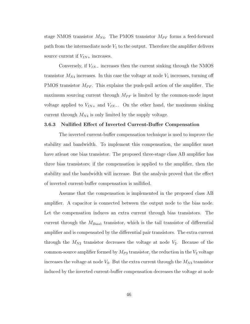
3.6.3 Nullified Effect of Inverted Current-Buffer Compensation
The inverted current-buffer compensation technique is used to improve the
stability and bandwidth. To implement this compensation, the amplifier must
have atleast one bias transistor. The proposed three-stage class AB amplifier has
three bias transistors; if the compensation is applied to the amplifier, then the
stability and the bandwidth will increase. But the analysis proved that the effect
of inverted current-buffer compensation is nullified.
Assume that the compensation is implemented in the proposed class AB
amplifier. A capacitor is connected between the output node to the bias node.
Let the compensation induces an extra current through bias transistors. The
current through the MBias1 transistor, which is the tail transistor of differential
amplifier and is compensated by the differential pair transistors. The extra current
through the MN2 transistor decreases the voltage at node V2. Because of the
common-source amplifier formed byMP3 transistor, the reduction in the V2 voltage
increases the voltage at node V3. But the extra current through the MN3 transistor
induced by the inverted current-buffer compensation decreases the voltage at node
46
V3 and balances the effect. This explains the nullified effect of inverted current-
buffer compensation.
RC1CC1
R1C1
V1 V2
gm1Vin R2C2gm2V1
CC3 RC3
R3C3gm3V2
RC4
ROutCOutgm4V3
CC2 RC2
gm4fV1
V3 VOut
Vin
G
+
–
S
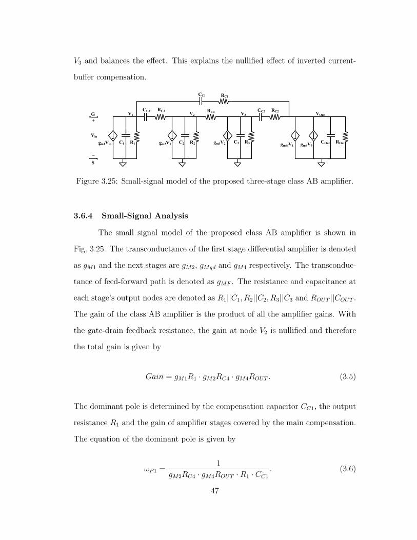
Figure 3.25: Small-signal model of the proposed three-stage class AB amplifier.
3.6.4 Small-Signal Analysis
The small signal model of the proposed class AB amplifier is shown in
Fig. 3.25. The transconductance of the first stage differential amplifier is denoted
as gM1 and the next stages are gM2, gMgd and gM4 respectively. The transconduc-
tance of feed-forward path is denoted as gMF . The resistance and capacitance at
each stage’s output nodes are denoted as R1||C1, R2||C2, R3||C3 and ROUT ||COUT .
The gain of the class AB amplifier is the product of all the amplifier gains. With
the gate-drain feedback resistance, the gain at node V2 is nullified and therefore
the total gain is given by
Gain = gM1R1 · gM2RC4 · gM4ROUT . (3.5)
The dominant pole is determined by the compensation capacitor CC1, the output
resistance R1 and the gain of amplifier stages covered by the main compensation.
The equation of the dominant pole is given by
ωP1 =1
gM2RC4 · gM4ROUT ·R1 · CC1
. (3.6)
47
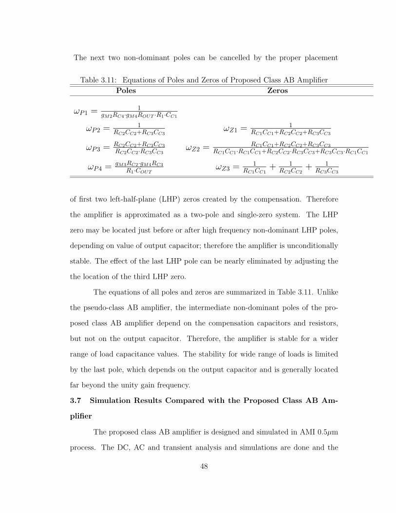
The next two non-dominant poles can be cancelled by the proper placement
Table 3.11: Equations of Poles and Zeros of Proposed Class AB Amplifier
Poles Zeros
ωP1 = 1gM2RC4·gM4ROUT ·R1·CC1
ωP2 = 1RC2CC2+RC3CC3
ωZ1 = 1RC1CC1+RC2CC2+RC3CC3
ωP3 = RC2CC2+RC3CC3
RC2CC2·RC3CC3ωZ2 = RC1CC1+RC2CC2+RC3CC3
RC1CC1·RC1CC1+RC2CC2·RC3CC3+RC3CC3·RC1CC1
ωP4 = gM3RC2·gM4RC3
R1·COUTωZ3 = 1
RC1CC1+ 1
RC2CC2+ 1
RC3CC3
of first two left-half-plane (LHP) zeros created by the compensation. Therefore
the amplifier is approximated as a two-pole and single-zero system. The LHP
zero may be located just before or after high frequency non-dominant LHP poles,
depending on value of output capacitor; therefore the amplifier is unconditionally
stable. The effect of the last LHP pole can be nearly eliminated by adjusting the
the location of the third LHP zero.
The equations of all poles and zeros are summarized in Table 3.11. Unlike
the pseudo-class AB amplifier, the intermediate non-dominant poles of the pro-
posed class AB amplifier depend on the compensation capacitors and resistors,
but not on the output capacitor. Therefore, the amplifier is stable for a wider
range of load capacitance values. The stability for wide range of loads is limited
by the last pole, which depends on the output capacitor and is generally located
far beyond the unity gain frequency.
3.7 Simulation Results Compared with the Proposed Class AB Am-
plifier
The proposed class AB amplifier is designed and simulated in AMI 0.5µm
process. The DC, AC and transient analysis and simulations are done and the
48

outputs are shown in the next subsections. The results of proposed class AB
amplifier is compared with the results of I-I-N and I-N-I pseudo-class AB amplifiers
and the results are summarized in Table. 3.12.
3.7.1 DC Analysis
DC currents are very important to characterize the amplifier as a class AB
or pseudo-class AB. DC analysis is used to plot the sourcing, sinking and quiescent
currents. The test bench for DC simulation is shown in Fig. 3.26. DC source is
given as the input to the amplifier in open-loop configuration and sweep the dc
voltage from -30mV to 30mV. The currents at the output stage and the total
quiescent currents are plotted. The dc currents of I-I-N, I-N-I pseudo-class AB,
I-N-I class AB and proposed class AB amplifiers are shown in Fig. 3.27, Fig. 3.28,
Fig. 3.29 and Fig. 3.30 respectively. For I-I-N pseudo-class AB amplifier, the
Vout
+
-
RLCL
VIN
+
+
-Amplifier
Figure 3.26: DC analysis test bench of proposed three-stage class AB amplifier.
quiescent current is low for huge sourcing current; as the sinking current increases,
the quiescent current goes very high as shown in Fig. 3.27. Conversely, in I-N-
I pseudo-class AB amplifier, the quiescent current increases with the sourcing
current as shown in Fig. 3.28. These results prove that the two amplifies are
pseudo-class AB amplifiers.
49
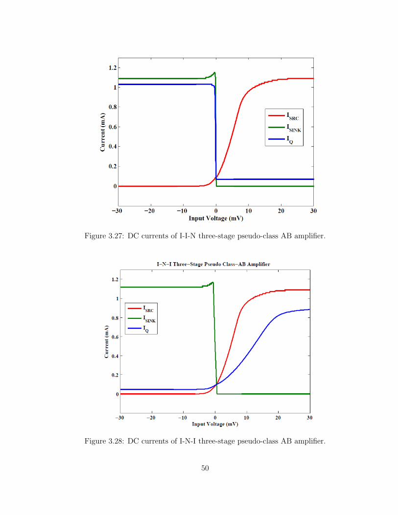
Figure 3.27: DC currents of I-I-N three-stage pseudo-class AB amplifier.
Figure 3.28: DC currents of I-N-I three-stage pseudo-class AB amplifier.
50
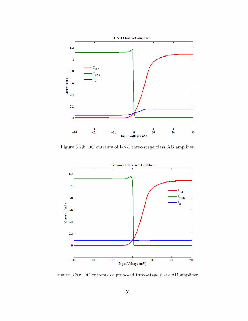
Figure 3.29: DC currents of I-N-I three-stage class AB amplifier.
Figure 3.30: DC currents of proposed three-stage class AB amplifier.
51

For I-N-I class AB amplifier, the quiescent current is very low for huge
sinking current and slightly higher for huge sourcing current as shown in Fig. 3.29.
The quiescent current is nearly constant even when the output current is increased.
This result prove that the amplifier is a true class AB amplifier.
The proposed class AB amplifier has nearly constant quiescent current for
huge sourcing and sinking currents as shown in Fig. 3.30. This result prove that
the proposed amplifier is a true class AB amplifier.
+
Vout
+
-
RLCL
VSIN
+
-
Amplifier
RLargeCLarge
AC magnitude =1
Phase = -180
Figure 3.31: AC analysis test bench of proposed three-stage class AB amplifier.
3.7.2 AC Analysis
The frequency analysis of the amplifiers are done by breaking the loop of
the amplifier with large resistor as shown in Fig. 3.31. The test bench has a AC
input source with ac magnitude is set to 1 and the phase is set to 180o, such
that the phase plot starts from 0o. AC simulation are done for different output
loads of 100pF||10kΩ, 200pF||1MΩ, and 25pF||1kΩ. The locations of poles and
zeros from the magnitude and phase plots are analysed and compared with the
52
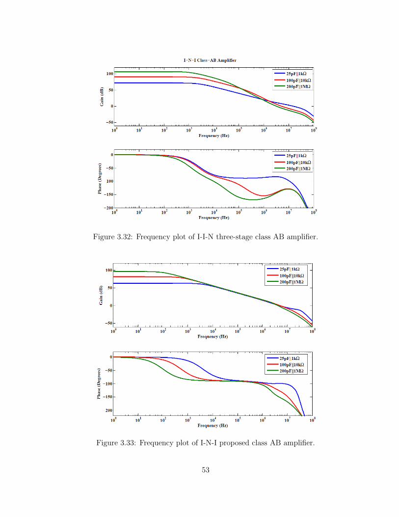
Figure 3.32: Frequency plot of I-I-N three-stage class AB amplifier.
Figure 3.33: Frequency plot of I-N-I proposed class AB amplifier.
53
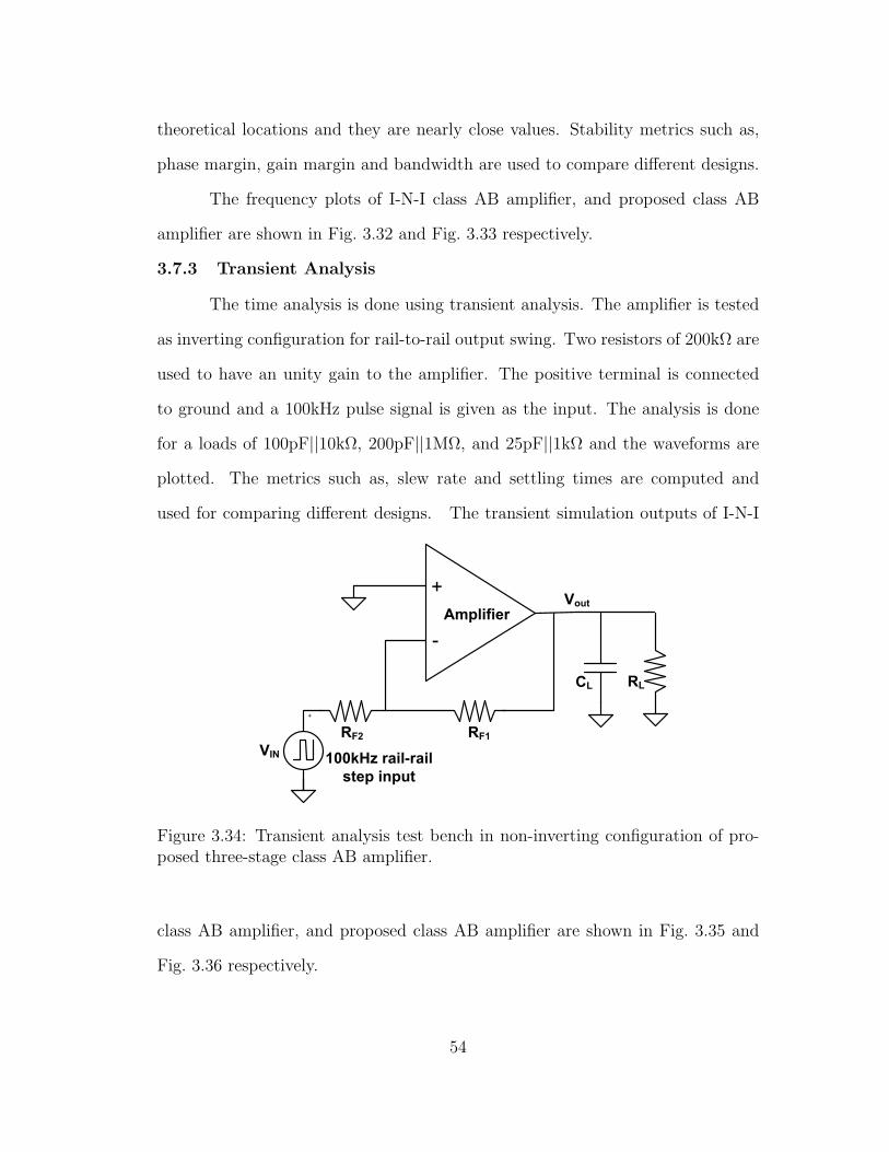
theoretical locations and they are nearly close values. Stability metrics such as,
phase margin, gain margin and bandwidth are used to compare different designs.
The frequency plots of I-N-I class AB amplifier, and proposed class AB
amplifier are shown in Fig. 3.32 and Fig. 3.33 respectively.
3.7.3 Transient Analysis
The time analysis is done using transient analysis. The amplifier is tested
as inverting configuration for rail-to-rail output swing. Two resistors of 200kΩ are
used to have an unity gain to the amplifier. The positive terminal is connected
to ground and a 100kHz pulse signal is given as the input. The analysis is done
for a loads of 100pF||10kΩ, 200pF||1MΩ, and 25pF||1kΩ and the waveforms are
plotted. The metrics such as, slew rate and settling times are computed and
used for comparing different designs. The transient simulation outputs of I-N-I
Vout
+
-
RLCL
VIN
+
-
Amplifier
RF1RF2
+
100kHz rail-rail
step input
Figure 3.34: Transient analysis test bench in non-inverting configuration of pro-posed three-stage class AB amplifier.
class AB amplifier, and proposed class AB amplifier are shown in Fig. 3.35 and
Fig. 3.36 respectively.
54
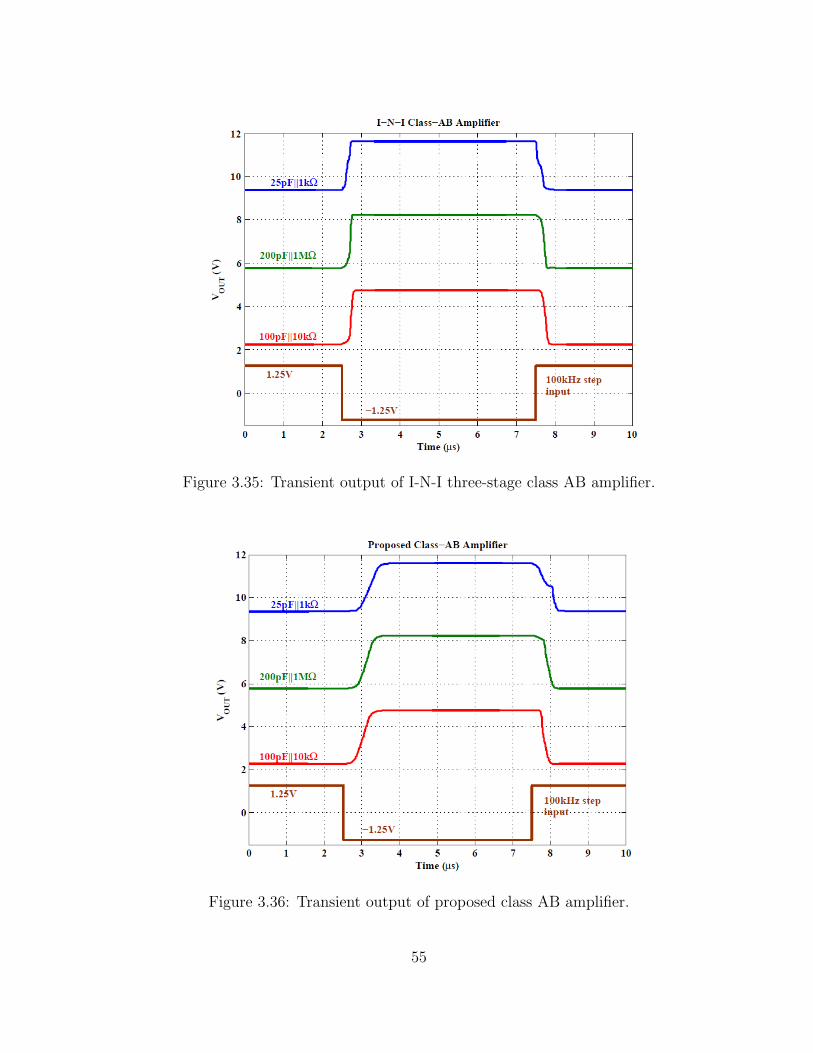
Figure 3.35: Transient output of I-N-I three-stage class AB amplifier.
Figure 3.36: Transient output of proposed class AB amplifier.
55
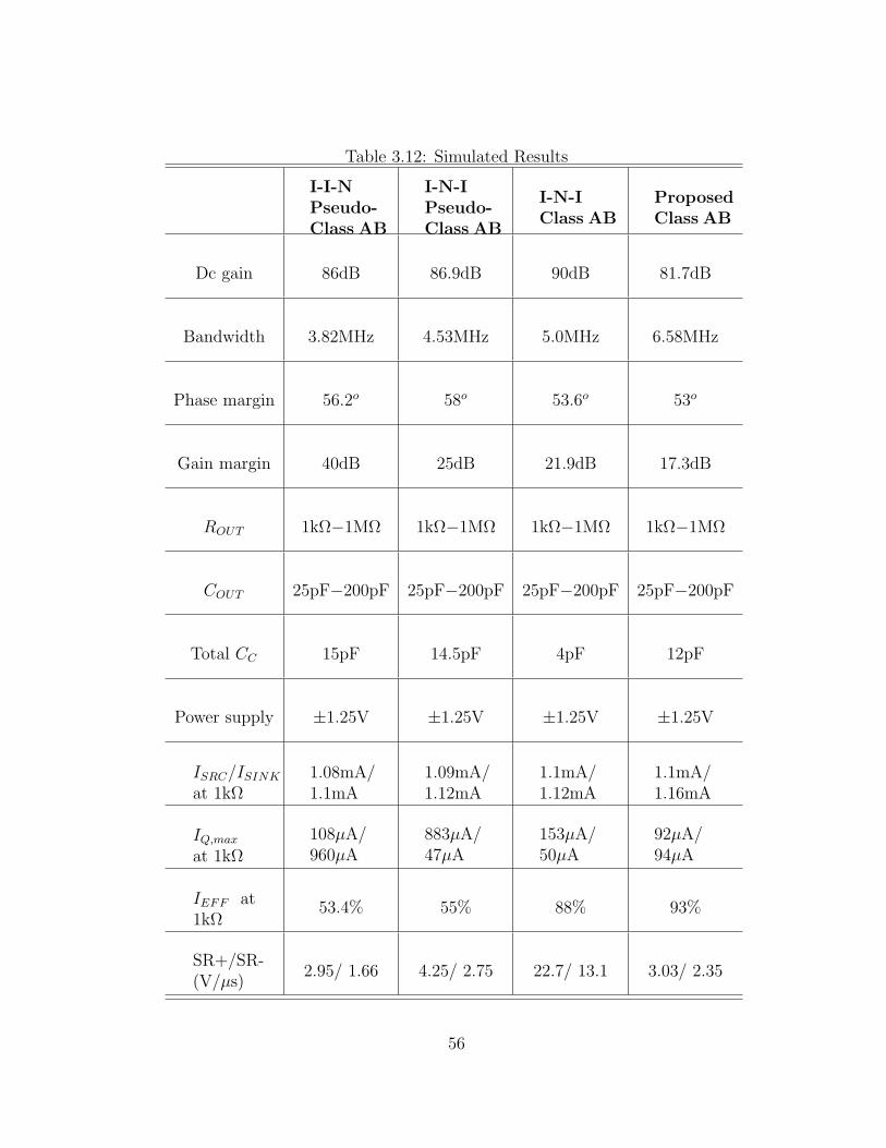
Table 3.12: Simulated Results
I-I-NPseudo-Class AB
I-N-IPseudo-Class AB
I-N-IClass AB
ProposedClass AB
Dc gain 86dB 86.9dB 90dB 81.7dB
Bandwidth 3.82MHz 4.53MHz 5.0MHz 6.58MHz
Phase margin 56.2o 58o 53.6o 53o
Gain margin 40dB 25dB 21.9dB 17.3dB
ROUT 1kΩ−1MΩ 1kΩ−1MΩ 1kΩ−1MΩ 1kΩ−1MΩ
COUT 25pF−200pF 25pF−200pF 25pF−200pF 25pF−200pF
Total CC 15pF 14.5pF 4pF 12pF
Power supply ±1.25V ±1.25V ±1.25V ±1.25V
ISRC/ISINK
at 1kΩ1.08mA/1.1mA
1.09mA/1.12mA
1.1mA/1.12mA
1.1mA/1.16mA
IQ,max
at 1kΩ
108µA/960µA
883µA/47µA
153µA/50µA
92µA/94µA
IEFF at1kΩ
53.4% 55% 88% 93%
SR+/SR-(V/µs)
2.95/ 1.66 4.25/ 2.75 22.7/ 13.1 3.03/ 2.35
56
Chapter 4
EXPERIMENTAL RESULTS
The layout of all the amplifiers and the microscopic view of chip and the hardware
results are discussed in this chapter.
4.1 Layout
The layout of all the amplifier are shown. The layout of I-I-N pseudo-
class AB amplifier is shown in Fig. 4.1. The area of the amplifier is around
263x191µm2. It has a minimum output driving load capacitance of 10µF, which
is also layed-out with the amplifier.
The layout of I-I-N pseudo-class AB with inverted current-buffer compen-
sation is shown in Fig. A.2. The area of the amplifier is around 226x183µm2. It
has a minimum output driving load capacitance of 10µF, which is also layed-out
with the amplifier.
The layout of I-N-I pseudo-class AB amplifier is shown in Fig. 4.3. The
area of the amplifier is around 173x170µm2.
The layout of proposed amplifier is shown in Fig. 4.4. The area of the
amplifier is around 177x167µm2.
The layout of overall chip is shown in Fig. 4.5. The chip contains 12
circuits in which, each of the above four amplifiers are repeated thrice. Two
sets of amplifiers are in open-loop configuration and one set of amplifiers are in
closed-loop configuration with unity gain.
57
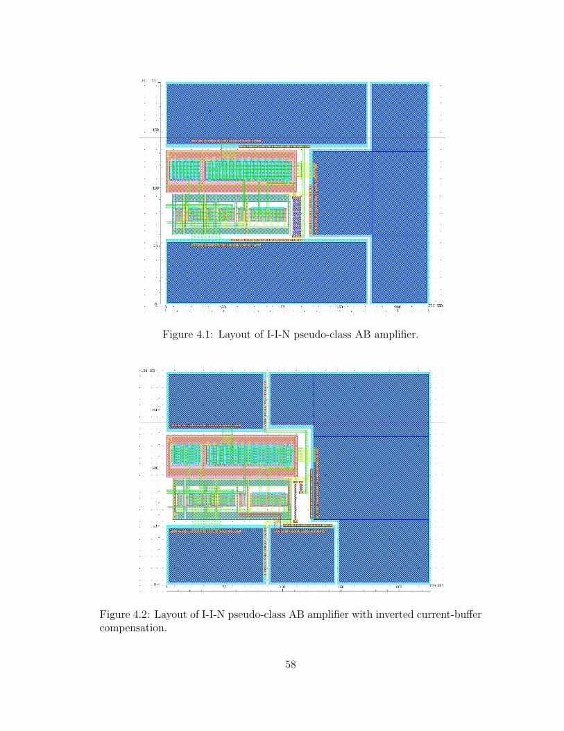
Figure 4.1: Layout of I-I-N pseudo-class AB amplifier.
Figure 4.2: Layout of I-I-N pseudo-class AB amplifier with inverted current-buffercompensation.
58
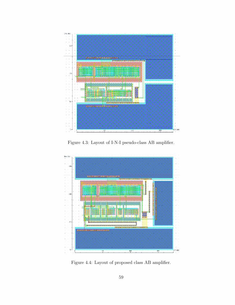
Figure 4.3: Layout of I-N-I pseudo-class AB amplifier.
Figure 4.4: Layout of proposed class AB amplifier.
59
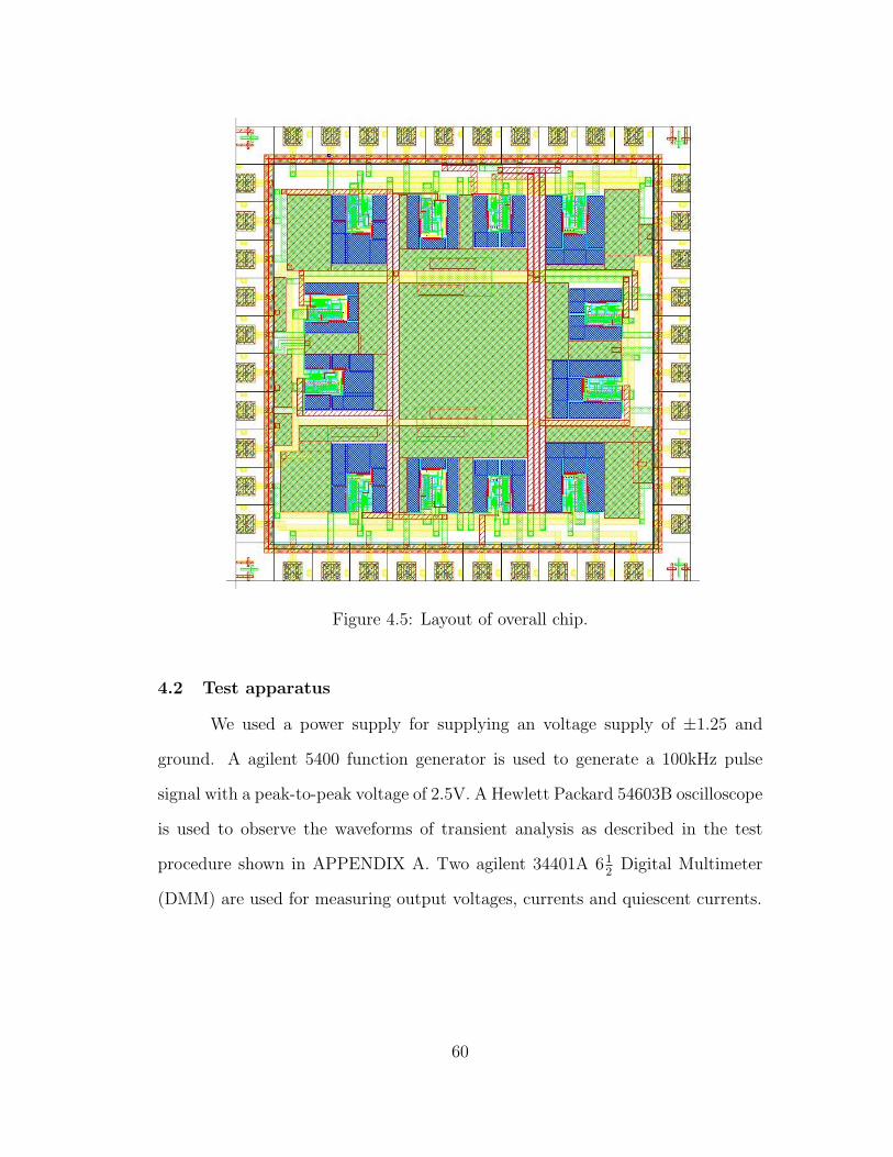
Figure 4.5: Layout of overall chip.
4.2 Test apparatus
We used a power supply for supplying an voltage supply of ±1.25 and
ground. A agilent 5400 function generator is used to generate a 100kHz pulse
signal with a peak-to-peak voltage of 2.5V. A Hewlett Packard 54603B oscilloscope
is used to observe the waveforms of transient analysis as described in the test
procedure shown in APPENDIX A. Two agilent 34401A 612
Digital Multimeter
(DMM) are used for measuring output voltages, currents and quiescent currents.
60
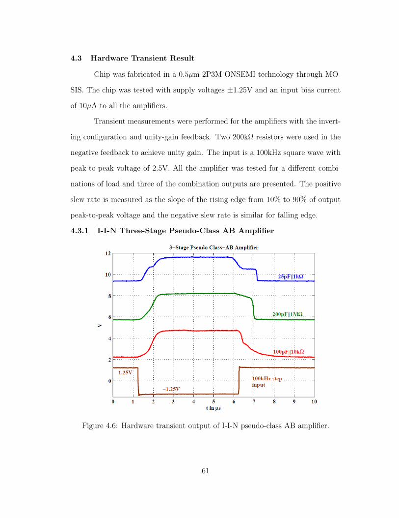
4.3 Hardware Transient Result
Chip was fabricated in a 0.5µm 2P3M ONSEMI technology through MO-
SIS. The chip was tested with supply voltages ±1.25V and an input bias current
of 10µA to all the amplifiers.
Transient measurements were performed for the amplifiers with the invert-
ing configuration and unity-gain feedback. Two 200kΩ resistors were used in the
negative feedback to achieve unity gain. The input is a 100kHz square wave with
peak-to-peak voltage of 2.5V. All the amplifier was tested for a different combi-
nations of load and three of the combination outputs are presented. The positive
slew rate is measured as the slope of the rising edge from 10% to 90% of output
peak-to-peak voltage and the negative slew rate is similar for falling edge.
4.3.1 I-I-N Three-Stage Pseudo-Class AB Amplifier
Figure 4.6: Hardware transient output of I-I-N pseudo-class AB amplifier.
61
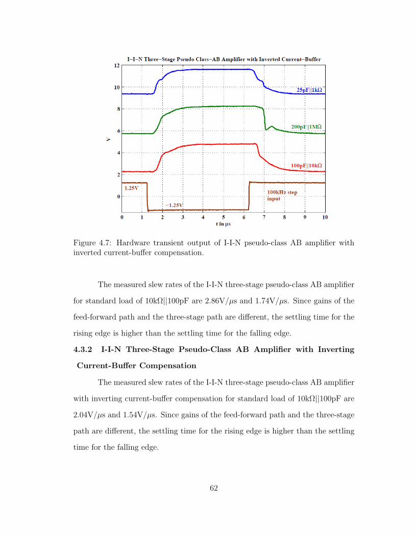
Figure 4.7: Hardware transient output of I-I-N pseudo-class AB amplifier withinverted current-buffer compensation.
The measured slew rates of the I-I-N three-stage pseudo-class AB amplifier
for standard load of 10kΩ||100pF are 2.86V/µs and 1.74V/µs. Since gains of the
feed-forward path and the three-stage path are different, the settling time for the
rising edge is higher than the settling time for the falling edge.
4.3.2 I-I-N Three-Stage Pseudo-Class AB Amplifier with Inverting
Current-Buffer Compensation
The measured slew rates of the I-I-N three-stage pseudo-class AB amplifier
with inverting current-buffer compensation for standard load of 10kΩ||100pF are
2.04V/µs and 1.54V/µs. Since gains of the feed-forward path and the three-stage
path are different, the settling time for the rising edge is higher than the settling
time for the falling edge.
62
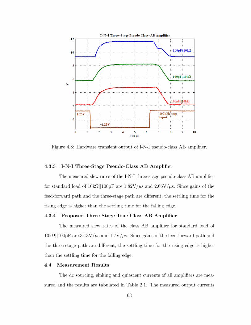
Figure 4.8: Hardware transient output of I-N-I pseudo-class AB amplifier.
4.3.3 I-N-I Three-Stage Pseudo-Class AB Amplifier
The measured slew rates of the I-N-I three-stage pseudo-class AB amplifier
for standard load of 10kΩ||100pF are 1.82V/µs and 2.66V/µs. Since gains of the
feed-forward path and the three-stage path are different, the settling time for the
rising edge is higher than the settling time for the falling edge.
4.3.4 Proposed Three-Stage True Class AB Amplifier
The measured slew rates of the class AB amplifier for standard load of
10kΩ||100pF are 3.13V/µs and 1.7V/µs. Since gains of the feed-forward path and
the three-stage path are different, the settling time for the rising edge is higher
than the settling time for the falling edge.
4.4 Measurement Results
The dc sourcing, sinking and quiescent currents of all amplifiers are mea-
sured and the results are tabulated in Table 2.1. The measured output currents
63
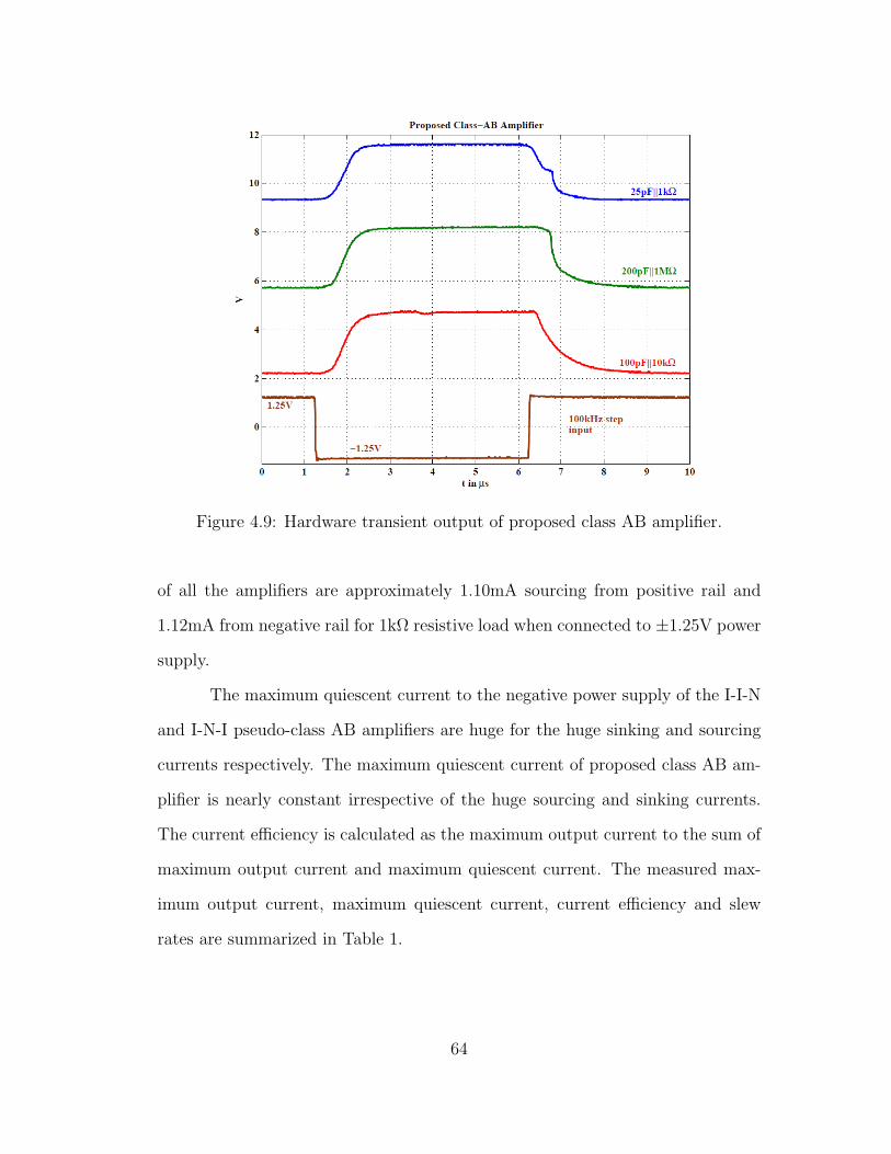
Figure 4.9: Hardware transient output of proposed class AB amplifier.
of all the amplifiers are approximately 1.10mA sourcing from positive rail and
1.12mA from negative rail for 1kΩ resistive load when connected to ±1.25V power
supply.
The maximum quiescent current to the negative power supply of the I-I-N
and I-N-I pseudo-class AB amplifiers are huge for the huge sinking and sourcing
currents respectively. The maximum quiescent current of proposed class AB am-
plifier is nearly constant irrespective of the huge sourcing and sinking currents.
The current efficiency is calculated as the maximum output current to the sum of
maximum output current and maximum quiescent current. The measured max-
imum output current, maximum quiescent current, current efficiency and slew
rates are summarized in Table 1.
64
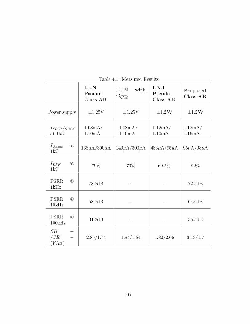
Table 4.1: Measured Results
I-I-NPseudo-Class AB
I-I-N withCCB
I-N-IPseudo-Class AB
ProposedClass AB
Power supply ±1.25V ±1.25V ±1.25V ±1.25V
ISRC/ISINK
at 1kΩ1.08mA/1.10mA
1.08mA/1.10mA
1.12mA/1.10mA
1.12mA/1.16mA
IQ,max at1kΩ
138µA/300µA 140µA/300µA 483µA/95µA 95µA/98µA
IEFF at1kΩ
79% 79% 69.5% 92%
PSRR @1kHz
78.2dB - - 72.5dB
PSRR @10kHz
58.7dB - - 64.0dB
PSRR @100kHz
31.3dB - - 36.3dB
SR +/SR −(V/µs)
2.86/1.74 1.84/1.54 1.82/2.66 3.13/1.7
65
Chapter 5
DISCUSSION AND CONCLUSION
The simulation and measurement results of proposed class AB amplifier is com-
pared with the pseudo-class AB amplifiers and are tabulated. The design of
proposed class AB amplifier is similar to the pseudo-class AB amplifier in low
supply-voltage, simple biasing, low transistor-count, wide output-swing and low
bias current. The results of class AB amplifier are comparable with the pseudo-
class AB amplifier in gain, phase margin, gain margin, and maximum output
current. But the proposed amplifier realizes the high current efficiency with low
quiescent current, increased in bandwidth, and decreased compensation capaci-
tance.
The class AB amplifier is stable for 500Ω of load resistance and has sourcing
and sinking currents of 2.1mA and 1.9mA. The amplifiers are also tested with a
power supply of ±2.0V to deliver a current of 1.98mA and 3.27mA of sourcing
currents and 1.97mA and 3.36mA of sinking currents for 1kΩ and 500Ω resistive
loads, respectively.
Finally, two different three-stage pseudo-class AB amplifiers are converted
to two different three-stage class AB amplifiers. The proposed class AB amplifier
has a higher current-efficiency and a higher bandwidth than the pseudo-class AB
amplifier. The poles and zeros of all the amplifiers are theoretically computed,
analysed and presented in the report. All the amplifiers are fabricated and the
results analysed in the simulation are verified by the experimental results.
66

5.0.1 Issues
The fabricated chip has 12 circuits of four different types. The four cir-
cuits are I-I-N pseudo-class AB amplifier, I-N-I pseudo-class AB amplifier, I-I-N
pseudo-class AB with inverted current-buffer compensation and proposed class AB
amplifier. Each of these circuits are repeated three times, two of them are open-
loop configuration and the third is of closed-loop configuration. The circuits of
the same kind have common bias pin. Therefore, we cannot be able to measure
quiescent current correctly. Therefore, we approximated the quiescent current by
subtracting the bias current of other two amplifiers.
And the other issue is that the internal nodes of multi-stage amplifiers
should be turned off. Otherwise, the nodes will be floating and may draw some
current through the transistors.
The I-I-N pseudo-class AB amplifier has a huge quiescent current when the
sinking current is huge. In a simulation, the quiescent current is approximately
900µA for a sinking current of 1.16mA. But the hardware results show that the
quiescent current is approximately 320µA for a sinking current of 1.15mA. We
were not able to find the reason because of a lack of time.
5.0.2 Anomalies
In this thesis we did not discuss the cross-over distortion. The pseudo-
class AB amplifiers and class AB amplifiers has a huge distortion. Our major
goal is to convert the widely-used pseudo-class AB amplifier to a true class AB
amplifier. Therefore, we did not consider the distortion of the amplifier.
5.0.3 Future Work
The proposed class AB amplifier is a true class AB amplifier. This is de-
signed as the general purpose amplifier. Therefore, the amplifier can be improved
as an application oriented amplifier such as audio amplifier, power amplifier, mo-
67
tor driver and LCD & LED driver. We need to deal with the distortion of the
class AB amplifiers.
The I-N-I class AB amplifier is working perfectly and the amplifier is not
fabricated. We did not complete the whole analysis on this class AB amplifier.
The I-N-I class AB amplifier is compensated with single inverted current-buffer
compensation which appears as nested inverted current-buffer compensation. The
amplifier is stable for very low resistive load of range 10Ω-1kΩ. Therefore, this
amplifier can be implemented as an audio amplifier for a resistive load of 16Ω.
68

APPENDICES

APPENDIX A
Test Document

A.1 Supply Voltages and Currents
VDD=1.25V
VSS=-1.25V
IBias=10µA
A.2 Procedure
1. Connect VDD (pin16) and VSS (pin36) and check whether the chip is good
or fired up.
2. Connect VDD (Pin16) to VDD1 (pin4) which is power supply to all the am-
plifiers that are on top
3. Attach bias resistor to each amplifier separately
• Three-Stage I-I-N Pseudo-Class AB Amplifier
The bias current is 10µA, the supply voltage VDD is 1.25V and Vbn1 is
-324.1mV . Therefore the bias resistor is given by
R =VDD − Vbn1
IBias
= 157.4kΩ (1)
Since it is supplying current to three amplifiers, the resistance should
be three times less than the calculated.
R = 53kΩ [Sincethreeamplifiers] (2)
Connect Vbn1 (pin8) to one end of the bias resistor and other end of
resistor is connected to VDD (Pin16)
71
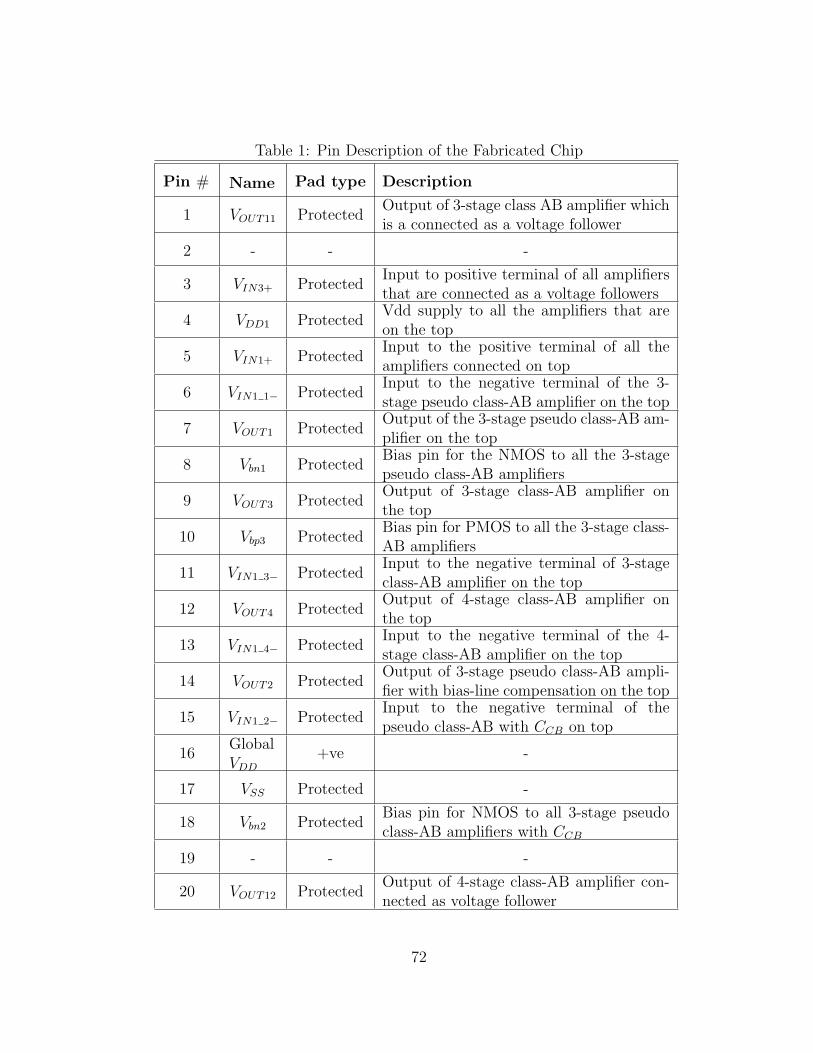
Table 1: Pin Description of the Fabricated Chip
Pin # Name Pad type Description
1 VOUT11 ProtectedOutput of 3-stage class AB amplifier whichis a connected as a voltage follower
2 - - -
3 VIN3+ ProtectedInput to positive terminal of all amplifiersthat are connected as a voltage followers
4 VDD1 ProtectedVdd supply to all the amplifiers that areon the top
5 VIN1+ ProtectedInput to the positive terminal of all theamplifiers connected on top
6 VIN1 1− ProtectedInput to the negative terminal of the 3-stage pseudo class-AB amplifier on the top
7 VOUT1 ProtectedOutput of the 3-stage pseudo class-AB am-plifier on the top
8 Vbn1 ProtectedBias pin for the NMOS to all the 3-stagepseudo class-AB amplifiers
9 VOUT3 ProtectedOutput of 3-stage class-AB amplifier onthe top
10 Vbp3 ProtectedBias pin for PMOS to all the 3-stage class-AB amplifiers
11 VIN1 3− ProtectedInput to the negative terminal of 3-stageclass-AB amplifier on the top
12 VOUT4 ProtectedOutput of 4-stage class-AB amplifier onthe top
13 VIN1 4− ProtectedInput to the negative terminal of the 4-stage class-AB amplifier on the top
14 VOUT2 ProtectedOutput of 3-stage pseudo class-AB ampli-fier with bias-line compensation on the top
15 VIN1 2− ProtectedInput to the negative terminal of thepseudo class-AB with CCB on top
16GlobalVDD
+ve -
17 VSS Protected -
18 Vbn2 ProtectedBias pin for NMOS to all 3-stage pseudoclass-AB amplifiers with CCB
19 - - -
20 VOUT12 ProtectedOutput of 4-stage class-AB amplifier con-nected as voltage follower
72
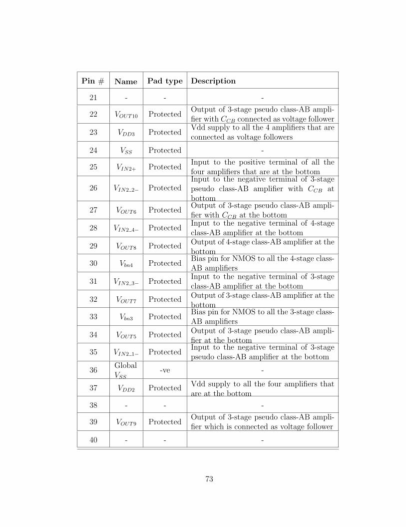
Pin # Name Pad type Description
21 - - -
22 VOUT10 ProtectedOutput of 3-stage pseudo class-AB ampli-fier with CCB connected as voltage follower
23 VDD3 ProtectedVdd supply to all the 4 amplifiers that areconnected as voltage followers
24 VSS Protected -
25 VIN2+ ProtectedInput to the positive terminal of all thefour amplifiers that are at the bottom
26 VIN2 2− ProtectedInput to the negative terminal of 3-stagepseudo class-AB amplifier with CCB atbottom
27 VOUT6 ProtectedOutput of 3-stage pseudo class-AB ampli-fier with CCB at the bottom
28 VIN2 4− ProtectedInput to the negative terminal of 4-stageclass-AB amplifier at the bottom
29 VOUT8 ProtectedOutput of 4-stage class-AB amplifier at thebottom
30 Vbn4 ProtectedBias pin for NMOS to all the 4-stage class-AB amplifiers
31 VIN2 3− ProtectedInput to the negative terminal of 3-stageclass-AB amplifier at the bottom
32 VOUT7 ProtectedOutput of 3-stage class-AB amplifier at thebottom
33 Vbn3 ProtectedBias pin for NMOS to all the 3-stage class-AB amplifiers
34 VOUT5 ProtectedOutput of 3-stage pseudo class-AB ampli-fier at the bottom
35 VIN2 1− ProtectedInput to the negative terminal of 3-stagepseudo class-AB amplifier at the bottom
36GlobalVSS
-ve -
37 VDD2 ProtectedVdd supply to all the four amplifiers thatare at the bottom
38 - - -
39 VOUT9 ProtectedOutput of 3-stage pseudo class-AB ampli-fier which is connected as voltage follower
40 - - -
73
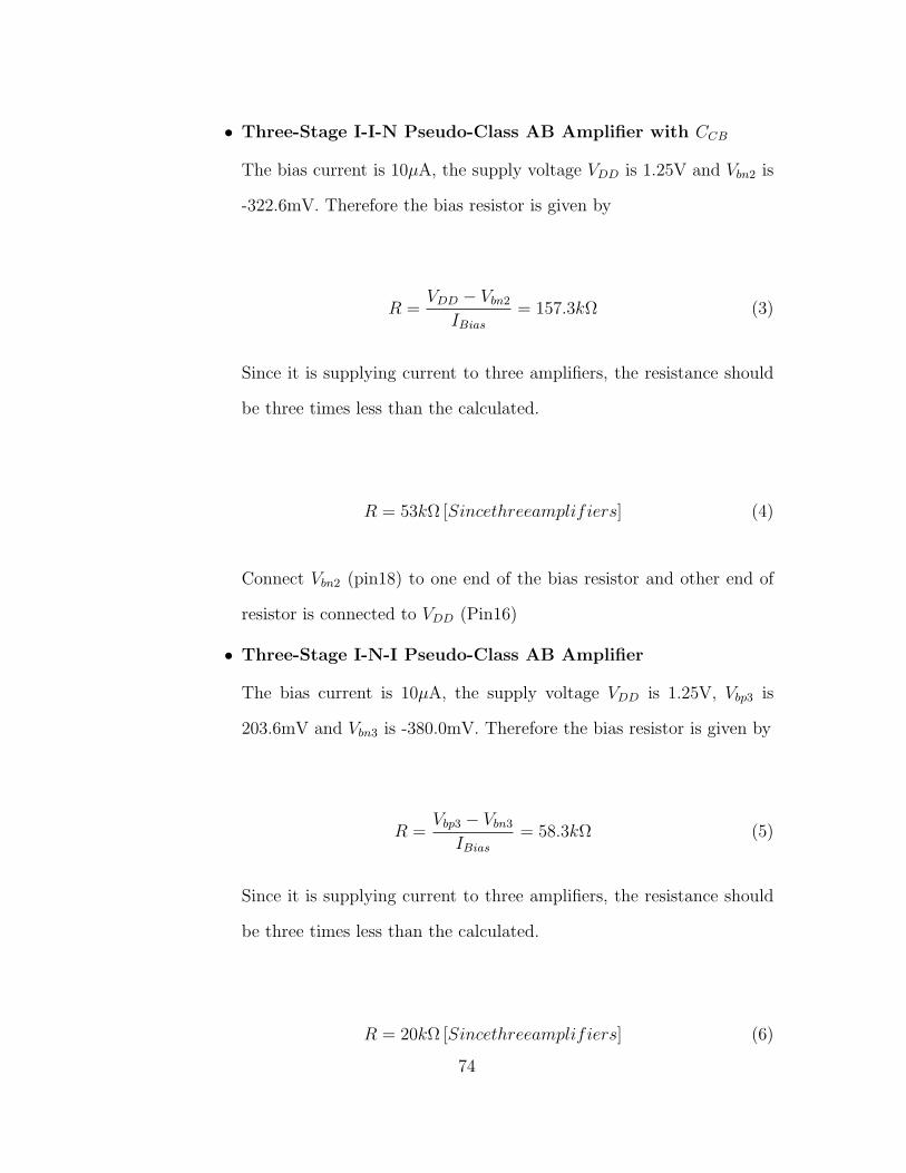
• Three-Stage I-I-N Pseudo-Class AB Amplifier with CCB
The bias current is 10µA, the supply voltage VDD is 1.25V and Vbn2 is
-322.6mV. Therefore the bias resistor is given by
R =VDD − Vbn2
IBias
= 157.3kΩ (3)
Since it is supplying current to three amplifiers, the resistance should
be three times less than the calculated.
R = 53kΩ [Sincethreeamplifiers] (4)
Connect Vbn2 (pin18) to one end of the bias resistor and other end of
resistor is connected to VDD (Pin16)
• Three-Stage I-N-I Pseudo-Class AB Amplifier
The bias current is 10µA, the supply voltage VDD is 1.25V, Vbp3 is
203.6mV and Vbn3 is -380.0mV. Therefore the bias resistor is given by
R =Vbp3 − Vbn3
IBias
= 58.3kΩ (5)
Since it is supplying current to three amplifiers, the resistance should
be three times less than the calculated.
R = 20kΩ [Sincethreeamplifiers] (6)
74
Connect Vbp3 (pin10) to one end of the bias resistor and other end of
resistor is connected to Vbn3 (Pin33)
• Three-Stage Proposed Class AB Amplifier
The bias current is 10µA, the supply voltage VDD is 1.25V and Vbn4 is
-380mV. Therefore the bias resistor is given by
R =VDD − Vbn4
IBias
= 163kΩ (7)
Since it is supplying current to three amplifiers, the resistance should
be three times less than the calculated.
R = 53.5kΩ [Sincethreeamplifiers] (8)
Connect Vbn4 (pin30) to one end of the bias resistor and other end of
resistor is connected to VDD (Pin16)
Transient Measurement
1. The amplifiers must be connected in inverting configuration as shown in
Fig. A.1.
2. Two 200kΩ resistors are used to achieve unity gain feedback
3. For three-stage I-I-N pseudo-class AB amplifier, a 200kΩ resistor is con-
nected in between VOUT1 (pin7) and VIN− (pin6) and another resistor to
VIN− (pin6) and the input from function generator
75
Vout
+
-
RLCL
VIN
+
-
I-I-N Pseudo
Class-AB
RF1RF2
+
100kHz rail-rail
step input
Figure A.1: Test bench for measuring transient response of the amplifier.
4. Similarly, for three-stage I-I-N pseudo-class AB amplifier with CCB, a 200kΩ
resistor is connected in between VOUT2 (pin14) and VIN− (pin15) and another
resistor to VIN− (pin15) and the input from function generator
5. For three-stage I-N-I pseudo-class AB amplifier, a 200kΩ resistor is con-
nected in between VOUT3 (pin9) and VIN− (pin11) and another resistor to
VIN− (pin11) and the input from function generator
6. For proposed three-stage class AB amplifier, a 200kΩ resistor is connected
in between VOUT4 (pin12) and VIN− (pin13) and another resistor to VIN−
(pin13) and the input from function generator
7. The positive terminal of all those amplifiers is shorted to VIN1+ (Pin5) and
it should be connected to ground of the function generator.
8. A rail-to tail pulse signal of frequency 100kHz from a function generator is
given to the 200kΩ resistor connected to negative terminal of the amplifiers.
76
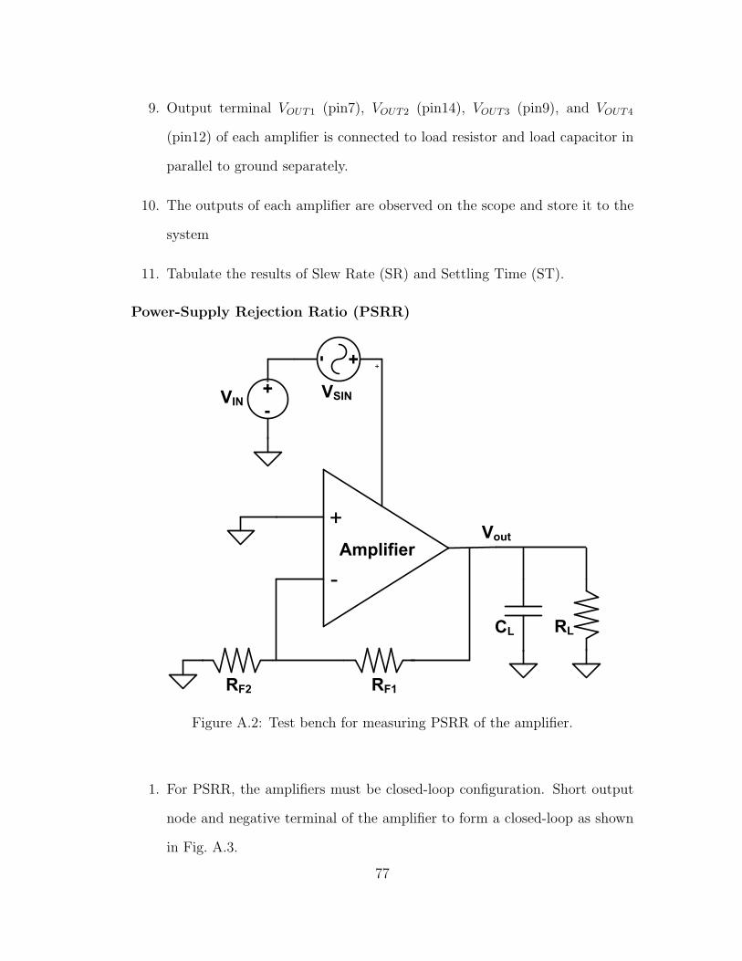
9. Output terminal VOUT1 (pin7), VOUT2 (pin14), VOUT3 (pin9), and VOUT4
(pin12) of each amplifier is connected to load resistor and load capacitor in
parallel to ground separately.
10. The outputs of each amplifier are observed on the scope and store it to the
system
11. Tabulate the results of Slew Rate (SR) and Settling Time (ST).
Power-Supply Rejection Ratio (PSRR)
Vout
+
-
RLCL
VIN
+
+
-
Amplifier
RF1RF2
+
VSIN
+
-
Figure A.2: Test bench for measuring PSRR of the amplifier.
1. For PSRR, the amplifiers must be closed-loop configuration. Short output
node and negative terminal of the amplifier to form a closed-loop as shown
in Fig. A.3.
77
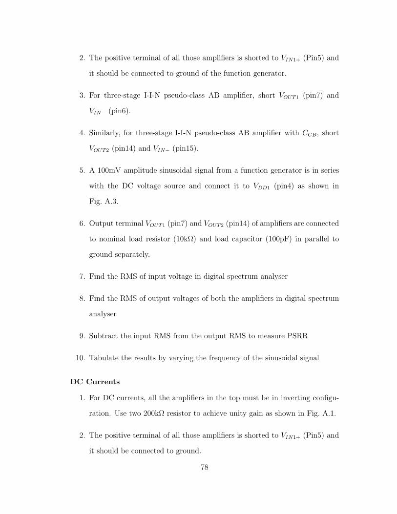
2. The positive terminal of all those amplifiers is shorted to VIN1+ (Pin5) and
it should be connected to ground of the function generator.
3. For three-stage I-I-N pseudo-class AB amplifier, short VOUT1 (pin7) and
VIN− (pin6).
4. Similarly, for three-stage I-I-N pseudo-class AB amplifier with CCB, short
VOUT2 (pin14) and VIN− (pin15).
5. A 100mV amplitude sinusoidal signal from a function generator is in series
with the DC voltage source and connect it to VDD1 (pin4) as shown in
Fig. A.3.
6. Output terminal VOUT1 (pin7) and VOUT2 (pin14) of amplifiers are connected
to nominal load resistor (10kΩ) and load capacitor (100pF) in parallel to
ground separately.
7. Find the RMS of input voltage in digital spectrum analyser
8. Find the RMS of output voltages of both the amplifiers in digital spectrum
analyser
9. Subtract the input RMS from the output RMS to measure PSRR
10. Tabulate the results by varying the frequency of the sinusoidal signal
DC Currents
1. For DC currents, all the amplifiers in the top must be in inverting configu-
ration. Use two 200kΩ resistor to achieve unity gain as shown in Fig. A.1.
2. The positive terminal of all those amplifiers is shorted to VIN1+ (Pin5) and
it should be connected to ground.
78
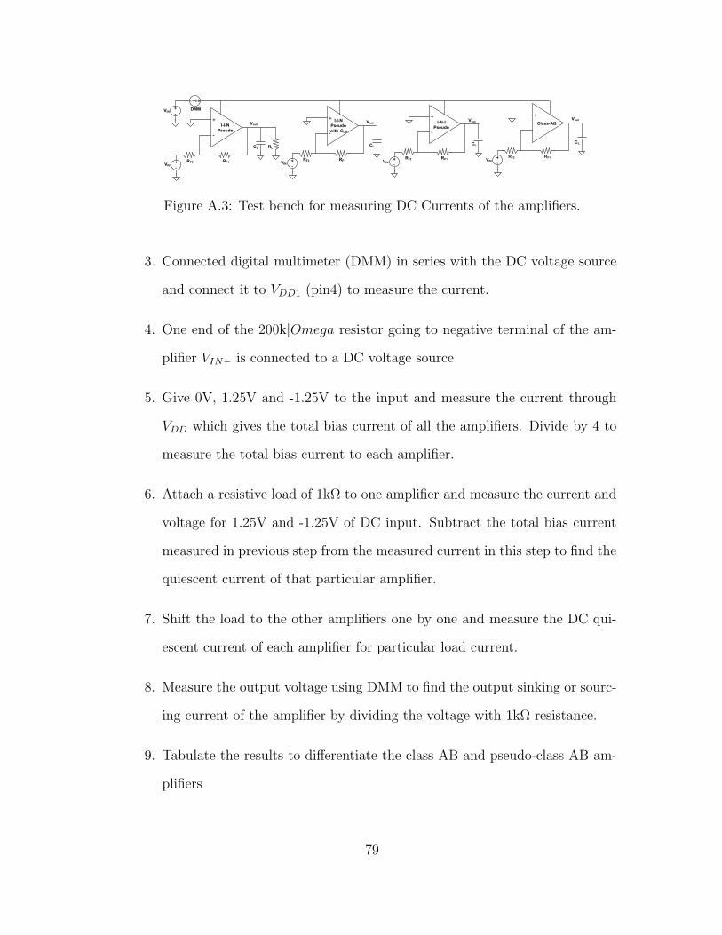
Vout
+
-
RLCL
VIN
+
+
-
I-I-N
Pseudo
RF1RF2
Vout
+
-
CL
VIN
+
+
-
RF1RF2
Vout
+
-
CL
VIN
+
+
-
I-N-I
Pseudo
RF1RF2
Vout
+
-
CL
VIN
+
+
-
Class-AB
RF1RF2
I-I-N
Pseudo
with CCB
VIN
+
+
-DMM
- +
Figure A.3: Test bench for measuring DC Currents of the amplifiers.
3. Connected digital multimeter (DMM) in series with the DC voltage source
and connect it to VDD1 (pin4) to measure the current.
4. One end of the 200k|Omega resistor going to negative terminal of the am-
plifier VIN− is connected to a DC voltage source
5. Give 0V, 1.25V and -1.25V to the input and measure the current through
VDD which gives the total bias current of all the amplifiers. Divide by 4 to
measure the total bias current to each amplifier.
6. Attach a resistive load of 1kΩ to one amplifier and measure the current and
voltage for 1.25V and -1.25V of DC input. Subtract the total bias current
measured in previous step from the measured current in this step to find the
quiescent current of that particular amplifier.
7. Shift the load to the other amplifiers one by one and measure the DC qui-
escent current of each amplifier for particular load current.
8. Measure the output voltage using DMM to find the output sinking or sourc-
ing current of the amplifier by dividing the voltage with 1kΩ resistance.
9. Tabulate the results to differentiate the class AB and pseudo-class AB am-
plifiers
79

APPENDIX B
Maple
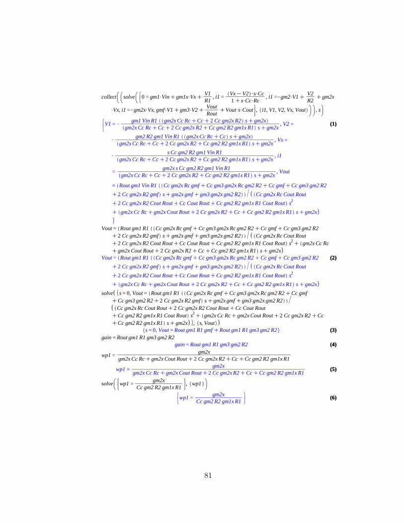
(3)(3)
(2)(2)
(1)(1)
(4)(4)
(6)(6)
(5)(5)
collect solve 0 = gm1$VinCgm1x$VxCV1R1
, i1 =VxKV2 $s$Cc1Cs$Cc$Rc
, i1 =Kgm2$V1CV2R2
Cgm2x
$Vx, i1 =Kgm2x$Vx, gmf$V1Cgm3$V2CVoutRout
CVout$s$Cout , i1, V1, V2, Vx, Vout , s
V1 =Kgm1 Vin R1 gm2x Cc RcCCcC2 Cc gm2x R2 sCgm2x
gm2x Cc RcCCcC2 Cc gm2x R2CCc gm2 R2 gm1x R1 sCgm2x, V2 =
Kgm2 R2 gm1 Vin R1 gm2x Cc RcCCc sCgm2x
gm2x Cc RcCCcC2 Cc gm2x R2CCc gm2 R2 gm1x R1 sCgm2x, Vx =
Ks Cc gm2 R2 gm1 Vin R1
gm2x Cc RcCCcC2 Cc gm2x R2CCc gm2 R2 gm1x R1 sCgm2x, i1
=gm2x s Cc gm2 R2 gm1 Vin R1
gm2x Cc RcCCcC2 Cc gm2x R2CCc gm2 R2 gm1x R1 sCgm2x, Vout
= Rout gm1 Vin R1 Cc gm2x Rc gmfCCc gm3 gm2x Rc gm2 R2CCc gmfCCc gm3 gm2 R2
C2 Cc gm2x R2 gmf sCgm2x gmfCgm3 gm2x gm2 R2 Cc gm2x Rc Cout Rout
C2 Cc gm2x R2 Cout RoutCCc Cout RoutCCc gm2 R2 gm1x R1 Cout Rout s2
C gm2x Cc RcCgm2x Cout RoutC2 Cc gm2x R2CCcCCc gm2 R2 gm1x R1 sCgm2x
Vout = Rout gm1 R1 Cc gm2x Rc gmfCCc gm3 gm2x Rc gm2 R2CCc gmfCCc gm3 gm2 R2C2 Cc gm2x R2 gmf sCgm2x gmfCgm3 gm2x gm2 R2 Cc gm2x Rc Cout RoutC2 Cc gm2x R2 Cout RoutCCc Cout RoutCCc gm2 R2 gm1x R1 Cout Rout s2
C gm2x Cc RcCgm2x Cout RoutC2 Cc gm2x R2CCcCCc gm2 R2 gm1x R1 sCgm2x
Vout = Rout gm1 R1 Cc gm2x Rc gmfCCc gm3 gm2x Rc gm2 R2CCc gmfCCc gm3 gm2 R2
C2 Cc gm2x R2 gmf sCgm2x gmfCgm3 gm2x gm2 R2 Cc gm2x Rc Cout Rout
C2 Cc gm2x R2 Cout RoutCCc Cout RoutCCc gm2 R2 gm1x R1 Cout Rout s2
C gm2x Cc RcCgm2x Cout RoutC2 Cc gm2x R2CCcCCc gm2 R2 gm1x R1 sCgm2x
solve s = 0, Vout = Rout gm1 R1 Cc gm2x Rc gmfCCc gm3 gm2x Rc gm2 R2CCc gmfCCc gm3 gm2 R2C2 Cc gm2x R2 gmf sCgm2x gmfCgm3 gm2x gm2 R2
Cc gm2x Rc Cout RoutC2 Cc gm2x R2 Cout RoutCCc Cout RoutCCc gm2 R2 gm1x R1 Cout Rout s2
C gm2x Cc RcCgm2x Cout RoutC2 Cc gm2x R2CCcCCc gm2 R2 gm1x R1 sCgm2x , s, Vout
s = 0, Vout = Rout gm1 R1 gmfCRout gm1 R1 gm3 gm2 R2gain = Rout gm1 R1 gm3 gm2 R2
gain = Rout gm1 R1 gm3 gm2 R2
wp1 =gm2x
gm2x Cc RcCgm2x Cout RoutC2 Cc gm2x R2CCcCCc gm2 R2 gm1x R1
wp1 =gm2x
gm2x Cc RcCgm2x Cout RoutC2 Cc gm2x R2CCcCCc gm2 R2 gm1x R1
solve wp1 =gm2x
Cc gm2 R2 gm1x R1, wp1
wp1 =gm2x
Cc gm2 R2 gm1x R1
81

REFERENCES
REFERENCES
[1] R. Mita, G. Palumbo, and S. Pennisi, “Design Guidelines for Reverse Nested
Miller Compensation in Three-Stage Amplifiers,” IEEE Trans. on Circuits
and Systems II, vol. 50, no. 5, pp. 227–233, May 2003.
[2] M. Rashid, A. Garimella, and P. Furth, “An Adaptive Biasing Technique
to Convert Pseudo-Class AB Amplifier to Class AB,” Electronics Letters,
vol. 46, no. 12, pp. 820–822, Jun. 2010.
[3] C.-W. Lu, “A Rail-To-Rail Class-AB Amplifier with an Offset Cancellation
for LCD Drivers,” IEEE J. Solid-State Circuits, vol. 44, no. 2, pp. 525–537,
Feb. 2009.
[4] R. J. Baker, CMOS Circuit Design, Layout, and Simulation, 3rd Edition.
Wiley-IEEE Press, 2000.
[5] M. Loikkanen and J. Kostamovaara, “Four-Stage 1.5V Class-AB Power Am-
plifier,” in Electrotechnical Conference, 2004. MELECON 2004. Proceedings
of the 12th IEEE Mediterranean, vol. 1, May 2004, p. 87.
[6] K. N. Leung and P. Mok, “Analysis of multi-stage amplifier-frequency com-
pensation,” IEEE Transactions on Circuits and Systems I: Fundamental The-
ory and Applications, vol. 48, no. 9, pp. 1041–1056, Sep. 2001.
[7] B. Razavi, Design of Analog CMOS Integrated Circuits. McGraw-Hill, 2000.
83
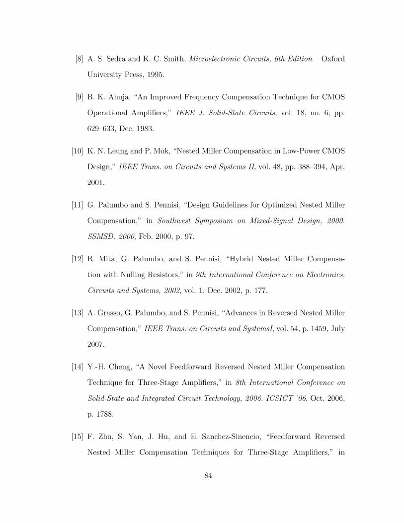
[8] A. S. Sedra and K. C. Smith, Microelectronic Circuits, 6th Edition. Oxford
University Press, 1995.
[9] B. K. Ahuja, “An Improved Frequency Compensation Technique for CMOS
Operational Amplifiers,” IEEE J. Solid-State Circuits, vol. 18, no. 6, pp.
629–633, Dec. 1983.
[10] K. N. Leung and P. Mok, “Nested Miller Compensation in Low-Power CMOS
Design,” IEEE Trans. on Circuits and Systems II, vol. 48, pp. 388–394, Apr.
2001.
[11] G. Palumbo and S. Pennisi, “Design Guidelines for Optimized Nested Miller
Compensation,” in Southwest Symposium on Mixed-Signal Design, 2000.
SSMSD. 2000, Feb. 2000, p. 97.
[12] R. Mita, G. Palumbo, and S. Pennisi, “Hybrid Nested Miller Compensa-
tion with Nulling Resistors,” in 9th International Conference on Electronics,
Circuits and Systems, 2002, vol. 1, Dec. 2002, p. 177.
[13] A. Grasso, G. Palumbo, and S. Pennisi, “Advances in Reversed Nested Miller
Compensation,” IEEE Trans. on Circuits and SystemsI, vol. 54, p. 1459, July
2007.
[14] Y.-H. Cheng, “A Novel Feedforward Reversed Nested Miller Compensation
Technique for Three-Stage Amplifiers,” in 8th International Conference on
Solid-State and Integrated Circuit Technology, 2006. ICSICT ’06, Oct. 2006,
p. 1788.
[15] F. Zhu, S. Yan, J. Hu, and E. Sanchez-Sinencio, “Feedforward Reversed
Nested Miller Compensation Techniques for Three-Stage Amplifiers,” in
84
IEEE International Symposium on Circuits and Systems, 2005. ISCAS 2005,
May 2005, p. 2575.
[16] J. Ramirez-Angulo, R. Carvajal, J. Galan, and A. Lopez-Martin, “A Free But
Efficient Low-Voltage Class-AB Two-Stage Operational Amplifier,” IEEE
Trans. on Circuits and SystemsII, vol. 53, no. 7, pp. 568–571, July 2006.
[17] G. Rincon-Mora and R. Stair, “A Low Voltage, Rail-to-Rail, Class AB CMOS
Amplifier with High Drive and Low Output Impedance Characteristics,”
IEEE Trans. on Circuits and SystemsII, vol. 48, no. 8, pp. 753–761, Aug.
2001.
[18] J.-H. Wang, J.-C. Qiu, H.-Y. Zheng, C.-H. Tsai, C.-Y. Wang, C.-C. Lee, and
C.-T. C. ;, “A Compact Low-Power High Slew-Rate Rail-to-Rail Class-AB
Buffer Amplifier for LCD Driver ICs,” Dec. 2007, p. 397.
[19] A. Garimella, M. Rashid, and P. Furth, “Reverse Nested Miller Compensation
Using Current Buffers in a Three-Stage LDO,” IEEE Trans. on Circuits and
Systems II, vol. 57, pp. 250–254, Apr. 2010.
[20] S.-C. Lee, K.-D. Kim, J.-K. Kwon, J. Kim, and S.-H. Lee, “A 10-bit 400-
MS/s 160-mW 0.13µm CMOS dual-channel pipeline ADC without channel
mismatch calibration,” IEEE Journal of Solid-State Circuits, vol. 41, pp.
1596–1605, Jul. 2006.
[21] A. D. Grasso, D. Marano, G. Palumbo, and S. Pennisi, “Improved Reversed
Nested Miller Frequency Compensation Technique with Voltage Buffer and
Resistor,” IEEE Trans. on Circuits and Systems II, vol. 54, pp. 382–386, May
2007.
85

[22] A. Grasso, P. Monsurro, S. Pennisi, G. Scotti, and A. Trifiletti, “Analysis and
Implementation of a Minimum-Supply Body-Biased CMOS Differential Am-
plifier Cell,” IEEE Trans. on Very Large Scale Integration (VLSI) Systems,
vol. 17, pp. 172–180, Feb. 2009.
86


![Pseudo Limits, Biadjoints, and Pseudo Algebras: Categorical ...arXiv:math/0408298v4 [math.CT] 18 Oct 2006 Pseudo Limits, Biadjoints, and Pseudo Algebras: Categorical Foundations of](https://img.pdfslide.us/doc/110x75/60a7a6d20b1ec1029337c248/pseudo-limits-biadjoints-and-pseudo-algebras-categorical-arxivmath0408298v4.jpg)