Embed Size (px)
Citation preview
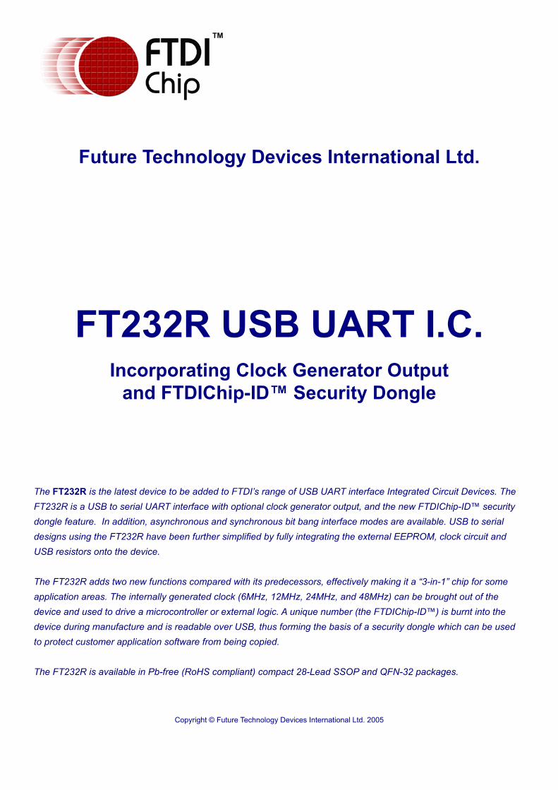
Future Technology Devices International Ltd.
Copyright © Future Technology Devices International Ltd. 2005
FT232R USB UART I.C.Incorporating Clock Generator Output
and FTDIChip-ID™ Security Dongle
The FT232R is the latest device to be added to FTDI’s range of USB UART interface Integrated Circuit Devices. The FT232R is a USB to serial UART interface with optional clock generator output, and the new FTDIChip-ID™ security dongle feature. In addition, asynchronous and synchronous bit bang interface modes are available. USB to serial designs using the FT232R have been further simplified by fully integrating the external EEPROM, clock circuit and USB resistors onto the device.
The FT232R adds two new functions compared with its predecessors, effectively making it a “3-in-1” chip for some application areas. The internally generated clock (6MHz, 12MHz, 24MHz, and 48MHz) can be brought out of the device and used to drive a microcontroller or external logic. A unique number (the FTDIChip-ID™) is burnt into the device during manufacture and is readable over USB, thus forming the basis of a security dongle which can be used to protect customer application software from being copied.
The FT232R is available in Pb-free (RoHS compliant) compact 28-Lead SSOP and QFN-32 packages.
™
FT232R USB UART I.C. Datasheet Version 1.04 © Future Technology Devices International Ltd. 2005
Page 2
• Single chip USB to asynchronous serial data transfer interface.
• Entire USB protocol handled on the chip - No USB-specific firmware programming required.
• UART interface support for 7 or 8 data bits, 1 or 2 stop bits and odd / even / mark / space / no parity.
• Fully assisted hardware or X-On / X-Off software handshaking.
• Data transfer rates from 300 baud to 3 Megabaud (RS422 / RS485 and at TTL levels) and 300 baud to 1 Megabaud (RS232).
• 256 byte receive buffer and 128 byte transmit buffer utilising buffer smoothing technology to allow for high data throughput.
• FTDI’s royalty-free VCP and D2XX drivers eliminate the requirement for USB driver development in most cases.
• In-built support for event characters and line break condition.
• New USB FTDIChip-ID™ feature.• New configurable CBUS I/O pins.• Auto transmit buffer control for RS485 applications.• Transmit and receive LED drive signals.• New 48MHz, 24MHz,12MHz, and 6MHz clock
output signal Options for driving external MCU or FPGA.
• FIFO receive and transmit buffers for high data throughput.
• Adjustable receive buffer timeout.• Synchronous and asynchronous bit bang mode
interface options with RD# and WR# strobes.• New CBUS bit bang mode option.
• Integrated 1024 Bit internal EEPROM for storing USB VID, PID, serial number and product description strings, and CBUS I/O configuration.
• Device supplied preprogrammed with unique USB serial number.
• Support for USB suspend and resume.• Support for bus powered, self powered, and high-
power bus powered USB configurations.• Integrated 3.3V level converter for USB I/O .• Integrated level converter on UART and CBUS for
interfacing to 5V - 1.8V Logic.• True 5V / 3.3V / 2.8V / 1.8V CMOS drive output
and TTL input.• High I/O pin output drive option.• Integrated USB resistors.• Integrated power-on-reset circuit.• Fully integrated clock - no external crystal,
oscillator, or resonator required.• Fully integrated AVCC supply filtering - No separate
AVCC pin and no external R-C filter required.• UART signal inversion option.• USB bulk transfer mode.• 3.3V to 5.25V Single Supply Operation.• Low operating and USB suspend current.• Low USB bandwidth consumption.• UHCI / OHCI / EHCI host controller compatible• USB 2.0 Full Speed compatible.• -40°C to 85°C extended operating temperature
range.• Available in compact Pb-free 28 Pin SSOP and
QFN-32 packages (both RoHS compliant).
1. Features 1.1 Hardware Features
Royalty-Free VIRTUAL COM PORT(VCP) DRIVERS for...• Windows 98, 98SE, ME, 2000, Server 2003, XP.• Windows Vista / Longhorn*• Windows XP 64-bit.*• Windows XP Embedded.• Windows CE.NET 4.2 & 5.0• MAC OS 8 / 9, OS-X• Linux 2.4 and greater
Royalty-Free D2XX Direct Drivers(USB Drivers + DLL S/W Interface)• Windows 98, 98SE, ME, 2000, Server 2003, XP.• Windows Vista / Longhorn*• Windows XP 64-bit.*• Windows XP Embedded.• Windows CE.NET 4.2 & 5.0• Linux 2.4 and greater
1.2 Driver Support
The drivers listed above are all available to download for free from the FTDI website. Various 3rd Party Drivers are also available for various other operating systems - see the FTDI website for details.* Currently Under Development. Contact FTDI for availability.
• USB to RS232 / RS422 / RS485 Converters• Upgrading Legacy Peripherals to USB• Cellular and Cordless Phone USB data transfer
cables and interfaces• Interfacing MCU / PLD / FPGA based designs to
USB • USB Audio and Low Bandwidth Video data transfer• PDA to USB data transfer• USB Smart Card Readers• USB Instrumentation
• USB Industrial Control • USB MP3 Player Interface• USB FLASH Card Reader / Writers• Set Top Box PC - USB interface• USB Digital Camera Interface• USB Hardware Modems• USB Wireless Modems• USB Bar Code Readers• USB Software / Hardware Encryption Dongles
1.3 Typical Applications
FT232R USB UART I.C. Datasheet Version 1.04 © Future Technology Devices International Ltd. 2005
Page 3
2. Enhancements
2.1 Device Enhancements and Key Features
This section summarises the enhancements and the key features of the FT232R device. For further details, consult the device pin-out description and functional description sections.
Integrated Clock Circuit - Previous generations of FTDI’s USB UART devices required an external crystal or ceramic resonator. The clock circuit has now been integrated onto the device meaning that no crystal or ceramic resonator is required. However, if required, an external 12MHz crystal can be used as the clock source.
Integrated EEPROM - Previous generations of FTDI’s USB UART devices required an external EEPROM if the device were to use USB Vendor ID (VID), Product ID (PID), serial number and product description strings other than the default values in the device itself. This external EEPROM has now been integrated onto the FT232R chip meaning that all designs have the option to change the product description strings. A user area of the internal EEPROM is available for storing additional data. The internal EEPROM is programmable in circuit, over USB without any additional voltage requirement.
Preprogrammed EEPROM - The FT232R is supplied with its internal EEPROM preprogrammed with a serial number which is unique to each individual device. This, in most cases, will remove the need to program the device EEPROM.
Integrated USB Resistors - Previous generations of FTDI’s USB UART devices required two external series resistors on the USBDP and USBDM lines, and a 1.5 kΩ pull up resistor on USBDP. These three resistors have now been integrated onto the device.
Integrated AVCC Filtering - Previous generations of FTDI’s USB UART devices had a separate AVCC pin - the supply to the internal PLL. This pin required an external R-C filter. The separate AVCC pin is now connected internally to VCC, and the filter has now been integrated onto the chip.
Less External Components - Integration of the crystal, EEPROM, USB resistors, and AVCC filter will substantially reduce the bill of materials cost for USB interface designs using the FT232R compared to its FT232BM predecessor.
Transmit and Receive Buffer Smoothing - The FT232R’s 256 byte receive buffer and 128 byte transmit buffer utilise new buffer smoothing technology to allow for high data throughput.
Configurable CBUS I/O Pin Options - There are now 5 configurable Control Bus (CBUS) lines. Options are TXDEN - transmit enable for RS485 designs, PWREN# - Power control for high power, bus powered designs, TXLED# - for pulsing an LED upon transmission of data, RXLED# - for pulsing an LED upon receiving data, TX&RXLED# - which will pulse an LED upon transmission OR reception of data, SLEEP# - indicates that the device going into USB suspend mode, CLK48 / CLK24 / CLK12 / CLK6 - 48MHz, 24MHz,12MHz, and 6MHz clock output signal options. There is also the option to bring out bit bang mode read and write strobes (see below). The CBUS lines can be configured with any one of these output options by setting bits in the internal EEPROM. The device is supplied with the most commonly used pin definitions preprogrammed - see Section 10 for details.
Enhanced Asynchronous Bit Bang Mode with RD# and WR# Strobes - The FT232R supports FTDI’s BM chip bit bang mode. In bit bang mode, the eight UART lines can be switched from the regular interface mode to an 8-bit general purpose I/O port. Data packets can be sent to the device and they will be sequentially sent to the interface at a rate controlled by an internal timer (equivalent to the baud rate prescaler). With the FT232R device this mode has been enhanced so that the internal RD# and WR# strobes are now brought out of the device which can be used to allow external logic to be clocked by accesses to the bit bang I/O bus. This option will be described more fully in a separate application note.
Synchronous Bit Bang Mode - Synchronous bit bang mode differs from asynchronous bit bang mode in that the interface pins are only read when the device is written to. Thus making it easier for the controlling program to measure the response to an output stimulus as the data returned is synchronous to the output data. The feature was previously seen in FTDI’s FT2232C device. This option will be described more fully in a separate application note.
CBUS Bit Bang Mode - This mode allows four of the CBUS pins to be individually configured as GPIO pins, similar to Asynchronous bit bang mode. It is possible to use this mode while the UART interface is being used, thus providing up to four general purpose I/O pins which are available during normal operation. An application note describing this feature is available separately from the FTDI website.
FT232R USB UART I.C. Datasheet Version 1.04 © Future Technology Devices International Ltd. 2005
Page 4
Lower Supply Voltage - Previous generations of the chip required 5V supply on the VCC pin. The FT232R will work with a Vcc supply in the range 3.3V - 5.25V. Bus powered designs would still take their supply from the 5V on the USB bus, but for self powered designs where only 3.3V is available and there is no 5V supply there is no longer any need for an additional external regulator.
Integrated Level Converter on UART Interface and Control Signals - VCCIO pin supply can be from 1.8V to 5V. Connecting the VCCIO pin to 1.8V, 2.8V, or 3.3V allows the device to directly interface to 1.8V, 2.8V or 3.3V and other logic families without the need for external level converter I.C. devices.
5V / 3.3V / 2.8V / 1.8V Logic Interface - The FT232R provides true CMOS Drive Outputs and TTL level Inputs.
Integrated Power-On-Reset (POR) Circuit- The device incorporates an internal POR function. A RESET# pin is available in order to allow external logic to reset the FT232R where required. However, for many applications the RESET# pin can be left unconnected, or pulled up to VCCIO.
Lower Operating and Suspend Current - The device operating supply current has been further reduced to 15mA, and the suspend current has been reduced to around 70μA. This allows greater margin for peripheral designs to meet the USB suspend current limit of 500μA.
Low USB Bandwidth Consumption - The operation of the USB interface to the FT232R has been designed to use as little as possible of the total USB bandwidth available from the USB host controller.
High Output Drive Option - The UART interface and CBUS I/O pins can be made to drive out at three times the standard signal drive level thus allowing multiple devices to be driven, or devices that require a greater signal drive strength to be interfaced to the FT232R. This option is enabled in the internal EEPROM.
Power Management Control for USB Bus Powered, High Current Designs- The PWREN# signal can be used to directly drive a transistor or P-Channel MOSFET in applications where power switching of external circuitry is required. An option in the internal EEPROM makes the device gently pull down on its UART interface lines when the power is shut off (PWREN# is high). In this mode any residual voltage on external circuitry is bled to GND when power is removed, thus ensuring that external circuitry controlled by PWREN# resets reliably when power is restored.
UART Pin Signal Inversion - The sense of each of the eight UART signals can be individually inverted by setting options in the internal EEPROM. Thus, CTS# (active low) can be changed to CTS (active high), or TXD can be changed to TXD#.
FTDIChip-ID™ - Each FT232R is assigned a unique number which is burnt into the device at manufacture. This ID number cannot be reprogrammed by product manufacturers or end-users. This allows the possibility of using FT232R based dongles for software licensing. Further to this, a renewable license scheme can be implemented based on the FTDIChip-ID™ number when encrypted with other information. This encrypted number can be stored in the user area of the FT232R internal EEPROM, and can be decrypted, then compared with the protected FTDIChip-ID™ to verify that a license is valid. Web based applications can be used to maintain product licensing this way. An application note describing this feature is available separately from the FTDI website.
Improved EMI Performance - The reduced operating current and improved on-chip VCC decoupling significantly improves the ease of PCB design requirements in order to meet FCC, CE and other EMI related specifications.
Programmable Receive Buffer Timeout - The receive buffer timeout is used to flush remaining data from the receive buffer. This time defaults to 16ms, but is programmable over USB in 1ms increments from 1ms to 255ms, thus allowing the device to be optimised for protocols that require fast response times from short data packets.
Extended Operating Temperature Range - The FT232R operates over an extended temperature range of -40º to +85º C thus allowing the device to be used in automotive and industrial applications.
New Package Options - The FT232R is available in two packages - a compact 28 pin SSOP ( FT232RL) and an ultra-compact 5mm x 5mm pinless QFN-32 package ( FT232RQ). Both packages are lead ( Pb ) free, and use a ‘green’ compound. Both packages are fully compliant with European Union directive 2002/95/EC.
FT232R USB UART I.C. Datasheet Version 1.04 © Future Technology Devices International Ltd. 2005
Page 5
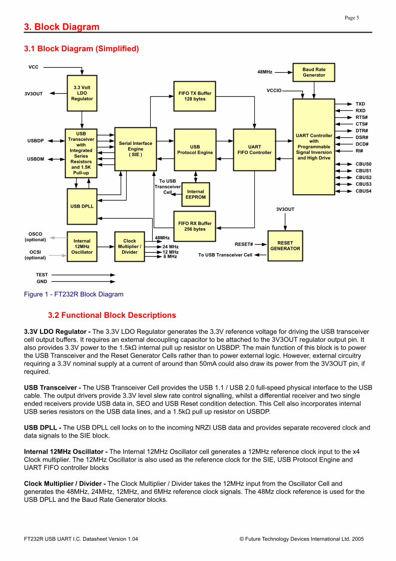
3. Block Diagram 3.1 Block Diagram (Simplified)
Figure 1 - FT232R Block Diagram
3.2 Functional Block Descriptions
3.3V LDO Regulator - The 3.3V LDO Regulator generates the 3.3V reference voltage for driving the USB transceiver cell output buffers. It requires an external decoupling capacitor to be attached to the 3V3OUT regulator output pin. It also provides 3.3V power to the 1.5kΩ internal pull up resistor on USBDP. The main function of this block is to power the USB Transceiver and the Reset Generator Cells rather than to power external logic. However, external circuitry requiring a 3.3V nominal supply at a current of around than 50mA could also draw its power from the 3V3OUT pin, if required.
USB Transceiver - The USB Transceiver Cell provides the USB 1.1 / USB 2.0 full-speed physical interface to the USB cable. The output drivers provide 3.3V level slew rate control signalling, whilst a differential receiver and two single ended receivers provide USB data in, SEO and USB Reset condition detection. This Cell also incorporates internal USB series resistors on the USB data lines, and a 1.5kΩ pull up resistor on USBDP.
USB DPLL - The USB DPLL cell locks on to the incoming NRZI USB data and provides separate recovered clock and data signals to the SIE block.
Internal 12MHz Oscillator - The Internal 12MHz Oscillator cell generates a 12MHz reference clock input to the x4 Clock multiplier. The 12MHz Oscillator is also used as the reference clock for the SIE, USB Protocol Engine and UART FIFO controller blocks
Clock Multiplier / Divider - The Clock Multiplier / Divider takes the 12MHz input from the Oscillator Cell and generates the 48MHz, 24MHz, 12MHz, and 6MHz reference clock signals. The 48Mz clock reference is used for the USB DPLL and the Baud Rate Generator blocks.
ClockMultiplier /
Divider
UARTFIFO Controller
Serial InterfaceEngine( SIE )
USBProtocol Engine
Baud RateGenerator
UART Controllerwith
ProgrammableSignal Inversionand High Drive
3.3 VoltLDO
Regulator
USBTransceiver
withIntegrated
SeriesResistorsand 1.5KPull-up
USB DPLL
Internal12MHz
Oscillator
48MHz
48MHz
OCSI(optional)
OSCO(optional)
USBDP
USBDM
3V3OUT
VCC
TXDRXDRTS#CTS#DTR#DSR#DCD#RI#
CBUS0
CBUS2CBUS3
RESET#
TESTGND
RESETGENERATOR
3V3OUT
CBUS1
FIFO TX Buffer128 bytes
FIFO RX Buffer256 bytes
InternalEEPROM
To USB Transceiver Cell
CBUS4
24 MHz12 MHz6 MHz
To USBTransceiver
Cell
VCCIO
FT232R USB UART I.C. Datasheet Version 1.04 © Future Technology Devices International Ltd. 2005
Page 6
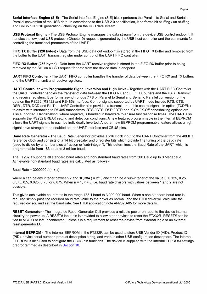
Serial Interface Engine (SIE) - The Serial Interface Engine (SIE) block performs the Parallel to Serial and Serial to Parallel conversion of the USB data. In accordance to the USB 2.0 specification, it performs bit stuffing / un-stuffing and CRC5 / CRC16 generation / checking on the USB data stream.
USB Protocol Engine - The USB Protocol Engine manages the data stream from the device USB control endpoint. It handles the low level USB protocol (Chapter 9) requests generated by the USB host controller and the commands for controlling the functional parameters of the UART.
FIFO TX Buffer (128 bytes) - Data from the USB data out endpoint is stored in the FIFO TX buffer and removed from the buffer to the UART transmit register under control of the UART FIFO controller.
FIFO RX Buffer (256 bytes) - Data from the UART receive register is stored in the FIFO RX buffer prior to being removed by the SIE on a USB request for data from the device data in endpoint.
UART FIFO Controller - The UART FIFO controller handles the transfer of data between the FIFO RX and TX buffers and the UART transmit and receive registers.
UART Controller with Programmable Signal Inversion and High Drive - Together with the UART FIFO Controller the UART Controller handles the transfer of data between the FIFO RX and FIFO TX buffers and the UART transmit and receive registers. It performs asynchronous 7 / 8 bit Parallel to Serial and Serial to Parallel conversion of the data on the RS232 (RS422 and RS485) interface. Control signals supported by UART mode include RTS, CTS, DSR , DTR, DCD and RI. The UART Controller also provides a transmitter enable control signal pin option (TXDEN) to assist with interfacing to RS485 transceivers. RTS / CTS, DSR / DTR and X-On / X-Off handshaking options are also supported. Handshaking, where required, is handled in hardware to ensure fast response times. The UART also supports the RS232 BREAK setting and detection conditions. A new feature, programmable in the internal EEPROM allows the UART signals to each be individually inverted. Another new EEPROM programmable feature allows a high signal drive strength to be enabled on the UART interface and CBUS pins.
Baud Rate Generator - The Baud Rate Generator provides a x16 clock input to the UART Controller from the 48MHz reference clock and consists of a 14 bit prescaler and 3 register bits which provide fine tuning of the baud rate (used to divide by a number plus a fraction or “sub-integer”). This determines the Baud Rate of the UART, which is programmable from 183 baud to 3 million baud.
The FT232R supports all standard baud rates and non-standard baud rates from 300 Baud up to 3 Megabaud. Achievable non-standard baud rates are calculated as follows -
Baud Rate = 3000000 / (n + x)
where n can be any integer between 2 and 16,384 ( = 214 ) and x can be a sub-integer of the value 0, 0.125, 0.25, 0.375, 0.5, 0.625, 0.75, or 0.875. When n = 1, x = 0, i.e. baud rate divisors with values between 1 and 2 are not possible.
This gives achievable baud rates in the range 183.1 baud to 3,000,000 baud. When a non-standard baud rate is required simply pass the required baud rate value to the driver as normal, and the FTDI driver will calculate the required divisor, and set the baud rate. See FTDI application note AN232B-05 for more details.
RESET Generator - The integrated Reset Generator Cell provides a reliable power-on reset to the device internal circuitry on power up. A RESET# input pin is provided to allow other devices to reset the FT232R. RESET# can be tied to VCCIO or left unconnected, unless it is a requirement to reset the device from external logic or an external reset generator I.C.
Internal EEPROM - The internal EEPROM in the FT232R can be used to store USB Vendor ID (VID), Product ID (PID), device serial number, product description string, and various other USB configuration descriptors. The internal EEPROM is also used to configure the CBUS pin functions. The device is supplied with the internal EEPROM settings preprogrammed as described in Section 10.
FT232R USB UART I.C. Datasheet Version 1.04 © Future Technology Devices International Ltd. 2005
Page 7
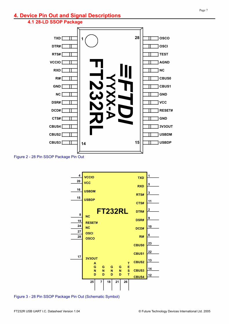
4. Device Pin Out and Signal Descriptions 4.1 28-LD SSOP Package
USBDP
USBDM
3V3OUT
GND
RESET#
VCC
GND
NC
AGND
TEST
OSCI
OSCO
CBUS1
CBUS0
TXD
RTS#
RXD
DTR#
VCCIO
RI#
GND
NC
DSR#
DCD#
CTS#
CBUS4
CBUS2
CBUS3F
T232R
LY
YX
X-A
1
14 15
28
FT
DI
Figure 2 - 28 Pin SSOP Package Pin Out
Figure 3 - 28 Pin SSOP Package Pin Out (Schematic Symbol)
FT232RL
AGND
GND
GND
GND
TEST
25 7 18 21 26
3V3OUT
VCCIO4
17
NC
RESET#
NC
24
19
8
TXD
RXD
RTS#
CTS#
DTR#
DSR#
DCD#
RI#
1
5
3
11
2
9
10
6
CBUS0
CBUS3
CBUS2
CBUS1
23
22
13
14
20
16
15USBDP
USBDM
VCC
OSCI27
OSCO28
CBUS4 12
FT232R USB UART I.C. Datasheet Version 1.04 © Future Technology Devices International Ltd. 2005
Page 8
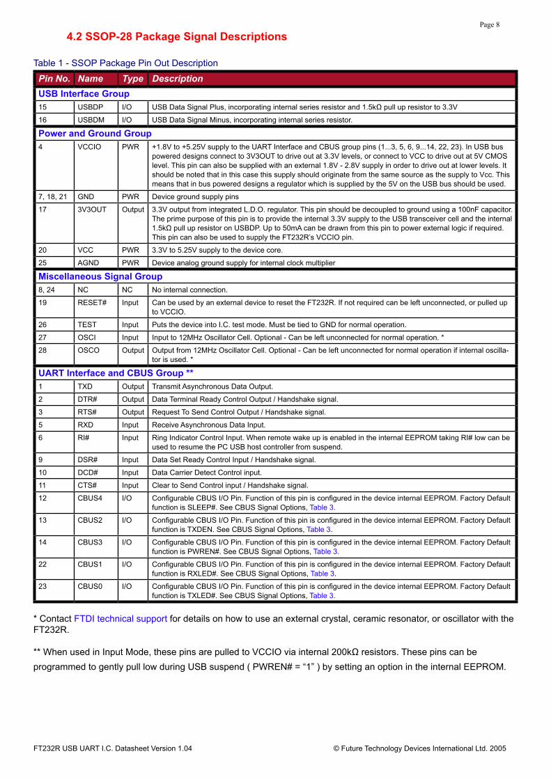
4.2 SSOP-28 Package Signal Descriptions
Table 1 - SSOP Package Pin Out Description
Pin No. Name Type DescriptionUSB Interface Group15 USBDP I/O USB Data Signal Plus, incorporating internal series resistor and 1.5kΩ pull up resistor to 3.3V
16 USBDM I/O USB Data Signal Minus, incorporating internal series resistor.
Power and Ground Group4 VCCIO PWR +1.8V to +5.25V supply to the UART Interface and CBUS group pins (1...3, 5, 6, 9...14, 22, 23). In USB bus
powered designs connect to 3V3OUT to drive out at 3.3V levels, or connect to VCC to drive out at 5V CMOS level. This pin can also be supplied with an external 1.8V - 2.8V supply in order to drive out at lower levels. It should be noted that in this case this supply should originate from the same source as the supply to Vcc. This means that in bus powered designs a regulator which is supplied by the 5V on the USB bus should be used.
7, 18, 21 GND PWR Device ground supply pins
17 3V3OUT Output 3.3V output from integrated L.D.O. regulator. This pin should be decoupled to ground using a 100nF capacitor. The prime purpose of this pin is to provide the internal 3.3V supply to the USB transceiver cell and the internal 1.5kΩ pull up resistor on USBDP. Up to 50mA can be drawn from this pin to power external logic if required. This pin can also be used to supply the FT232R’s VCCIO pin.
20 VCC PWR 3.3V to 5.25V supply to the device core.
25 AGND PWR Device analog ground supply for internal clock multiplier
Miscellaneous Signal Group8, 24 NC NC No internal connection.
19 RESET# Input Can be used by an external device to reset the FT232R. If not required can be left unconnected, or pulled up to VCCIO.
26 TEST Input Puts the device into I.C. test mode. Must be tied to GND for normal operation.
27 OSCI Input Input to 12MHz Oscillator Cell. Optional - Can be left unconnected for normal operation. *
28 OSCO Output Output from 12MHz Oscillator Cell. Optional - Can be left unconnected for normal operation if internal oscilla-tor is used. *
UART Interface and CBUS Group **1 TXD Output Transmit Asynchronous Data Output.
2 DTR# Output Data Terminal Ready Control Output / Handshake signal.
3 RTS# Output Request To Send Control Output / Handshake signal.
5 RXD Input Receive Asynchronous Data Input.
6 RI# Input Ring Indicator Control Input. When remote wake up is enabled in the internal EEPROM taking RI# low can be used to resume the PC USB host controller from suspend.
9 DSR# Input Data Set Ready Control Input / Handshake signal.
10 DCD# Input Data Carrier Detect Control input.
11 CTS# Input Clear to Send Control input / Handshake signal.
12 CBUS4 I/O Configurable CBUS I/O Pin. Function of this pin is configured in the device internal EEPROM. Factory Default function is SLEEP#. See CBUS Signal Options, Table 3.
13 CBUS2 I/O Configurable CBUS I/O Pin. Function of this pin is configured in the device internal EEPROM. Factory Default function is TXDEN. See CBUS Signal Options, Table 3.
14 CBUS3 I/O Configurable CBUS I/O Pin. Function of this pin is configured in the device internal EEPROM. Factory Default function is PWREN#. See CBUS Signal Options, Table 3.
22 CBUS1 I/O Configurable CBUS I/O Pin. Function of this pin is configured in the device internal EEPROM. Factory Default function is RXLED#. See CBUS Signal Options, Table 3.
23 CBUS0 I/O Configurable CBUS I/O Pin. Function of this pin is configured in the device internal EEPROM. Factory Default function is TXLED#. See CBUS Signal Options, Table 3.
* Contact FTDI technical support for details on how to use an external crystal, ceramic resonator, or oscillator with the FT232R.
** When used in Input Mode, these pins are pulled to VCCIO via internal 200kΩ resistors. These pins can be programmed to gently pull low during USB suspend ( PWREN# = “1” ) by setting an option in the internal EEPROM.
FT232R USB UART I.C. Datasheet Version 1.04 © Future Technology Devices International Ltd. 2005
Page 9
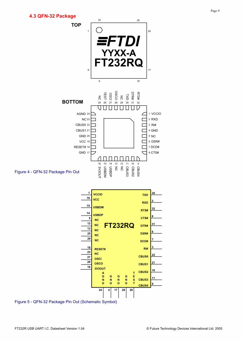
4.3 QFN-32 Package
Figure 4 - QFN-32 Package Pin Out
FT232RQ
AGND
GND
GND
GND
TEST
24 4 17 20 26
3V3OUT
VCCIO1
16
NC
RESET#
NC
23
18
13
TXD
RXD
RTS#
CTS#
DTR#
DSR#
DCD#
RI#
30
2
32
8
31
6
7
3
CBUS0
CBUS3
CBUS2
CBUS1
22
21
10
11
19
15
14USBDP
USBDM
VCC
OSCI27
OSCO28
CBUS4 9
NC12NC5
NC29NC25
Figure 5 - QFN-32 Package Pin Out (Schematic Symbol)
FT232RQ
32 25
24
17
169
8
1
YYXX-A
18
9
1
2
3
4
5
6
7
8
10111213141516
17
19
20
21
22
23
24
25 26 27 28 29 30 31 32
US
BD
P
US
BD
M
3V3O
UT
RESET#
VCC
NC
AGND
TE
ST
OS
CI
OS
CO
CBUS1
CBUS0
TX
D
RT
S#
RXD
DT
R#
VCCIO
RI#
GND
NC
DSR#
DCD#
CTS#
CB
US
4
CB
US
2
CB
US
3
GND
GND
NC
NC
NC
NC
FTDITOP
BOTTOM
FT232R USB UART I.C. Datasheet Version 1.04 © Future Technology Devices International Ltd. 2005
Page 10
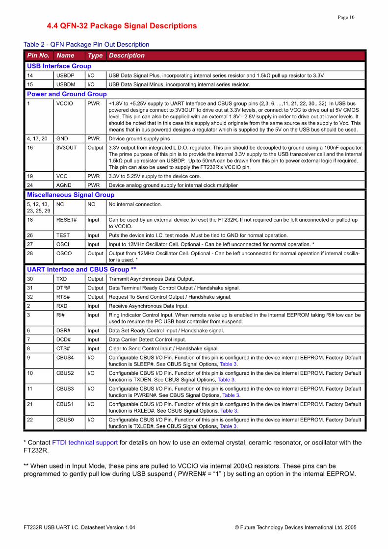
4.4 QFN-32 Package Signal Descriptions
Table 2 - QFN Package Pin Out Description
Pin No. Name Type DescriptionUSB Interface Group14 USBDP I/O USB Data Signal Plus, incorporating internal series resistor and 1.5kΩ pull up resistor to 3.3V
15 USBDM I/O USB Data Signal Minus, incorporating internal series resistor.
Power and Ground Group1 VCCIO PWR +1.8V to +5.25V supply to UART Interface and CBUS group pins (2,3, 6, ...,11, 21, 22, 30,..32). In USB bus
powered designs connect to 3V3OUT to drive out at 3.3V levels, or connect to VCC to drive out at 5V CMOS level. This pin can also be supplied with an external 1.8V - 2.8V supply in order to drive out at lower levels. It should be noted that in this case this supply should originate from the same source as the supply to Vcc. This means that in bus powered designs a regulator which is supplied by the 5V on the USB bus should be used.
4, 17, 20 GND PWR Device ground supply pins
16 3V3OUT Output 3.3V output from integrated L.D.O. regulator. This pin should be decoupled to ground using a 100nF capacitor. The prime purpose of this pin is to provide the internal 3.3V supply to the USB transceiver cell and the internal 1.5kΩ pull up resistor on USBDP. Up to 50mA can be drawn from this pin to power external logic if required. This pin can also be used to supply the FT232R’s VCCIO pin.
19 VCC PWR 3.3V to 5.25V supply to the device core.
24 AGND PWR Device analog ground supply for internal clock multiplier
Miscellaneous Signal Group5, 12, 13, 23, 25, 29
NC NC No internal connection.
18 RESET# Input Can be used by an external device to reset the FT232R. If not required can be left unconnected or pulled up to VCCIO.
26 TEST Input Puts the device into I.C. test mode. Must be tied to GND for normal operation.
27 OSCI Input Input to 12MHz Oscillator Cell. Optional - Can be left unconnected for normal operation. *
28 OSCO Output Output from 12MHz Oscillator Cell. Optional - Can be left unconnected for normal operation if internal oscilla-tor is used. *
UART Interface and CBUS Group **30 TXD Output Transmit Asynchronous Data Output.
31 DTR# Output Data Terminal Ready Control Output / Handshake signal.
32 RTS# Output Request To Send Control Output / Handshake signal.
2 RXD Input Receive Asynchronous Data Input.
3 RI# Input Ring Indicator Control Input. When remote wake up is enabled in the internal EEPROM taking RI# low can be used to resume the PC USB host controller from suspend.
6 DSR# Input Data Set Ready Control Input / Handshake signal.
7 DCD# Input Data Carrier Detect Control input.
8 CTS# Input Clear to Send Control input / Handshake signal.
9 CBUS4 I/O Configurable CBUS I/O Pin. Function of this pin is configured in the device internal EEPROM. Factory Default function is SLEEP#. See CBUS Signal Options, Table 3.
10 CBUS2 I/O Configurable CBUS I/O Pin. Function of this pin is configured in the device internal EEPROM. Factory Default function is TXDEN. See CBUS Signal Options, Table 3.
11 CBUS3 I/O Configurable CBUS I/O Pin. Function of this pin is configured in the device internal EEPROM. Factory Default function is PWREN#. See CBUS Signal Options, Table 3.
21 CBUS1 I/O Configurable CBUS I/O Pin. Function of this pin is configured in the device internal EEPROM. Factory Default function is RXLED#. See CBUS Signal Options, Table 3.
22 CBUS0 I/O Configurable CBUS I/O Pin. Function of this pin is configured in the device internal EEPROM. Factory Default function is TXLED#. See CBUS Signal Options, Table 3.
* Contact FTDI technical support for details on how to use an external crystal, ceramic resonator, or oscillator with the FT232R.
** When used in Input Mode, these pins are pulled to VCCIO via internal 200kΩ resistors. These pins can be programmed to gently pull low during USB suspend ( PWREN# = “1” ) by setting an option in the internal EEPROM.
FT232R USB UART I.C. Datasheet Version 1.04 © Future Technology Devices International Ltd. 2005
Page 11
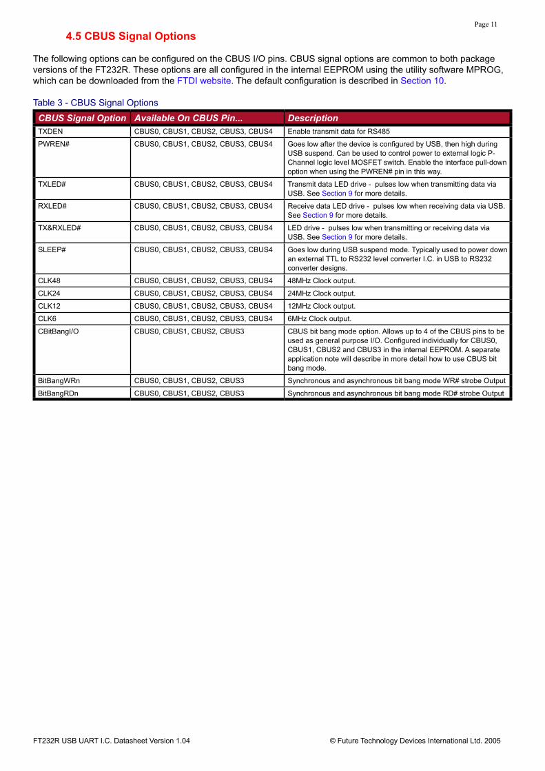
4.5 CBUS Signal Options
The following options can be configured on the CBUS I/O pins. CBUS signal options are common to both package versions of the FT232R. These options are all configured in the internal EEPROM using the utility software MPROG, which can be downloaded from the FTDI website. The default configuration is described in Section 10.
Table 3 - CBUS Signal Options
CBUS Signal Option Available On CBUS Pin... DescriptionTXDEN CBUS0, CBUS1, CBUS2, CBUS3, CBUS4 Enable transmit data for RS485
PWREN# CBUS0, CBUS1, CBUS2, CBUS3, CBUS4 Goes low after the device is configured by USB, then high during USB suspend. Can be used to control power to external logic P-Channel logic level MOSFET switch. Enable the interface pull-down option when using the PWREN# pin in this way.
TXLED# CBUS0, CBUS1, CBUS2, CBUS3, CBUS4 Transmit data LED drive - pulses low when transmitting data via USB. See Section 9 for more details.
RXLED# CBUS0, CBUS1, CBUS2, CBUS3, CBUS4 Receive data LED drive - pulses low when receiving data via USB. See Section 9 for more details.
TX&RXLED# CBUS0, CBUS1, CBUS2, CBUS3, CBUS4 LED drive - pulses low when transmitting or receiving data via USB. See Section 9 for more details.
SLEEP# CBUS0, CBUS1, CBUS2, CBUS3, CBUS4 Goes low during USB suspend mode. Typically used to power down an external TTL to RS232 level converter I.C. in USB to RS232 converter designs.
CLK48 CBUS0, CBUS1, CBUS2, CBUS3, CBUS4 48MHz Clock output.
CLK24 CBUS0, CBUS1, CBUS2, CBUS3, CBUS4 24MHz Clock output.
CLK12 CBUS0, CBUS1, CBUS2, CBUS3, CBUS4 12MHz Clock output.
CLK6 CBUS0, CBUS1, CBUS2, CBUS3, CBUS4 6MHz Clock output.
CBitBangI/O CBUS0, CBUS1, CBUS2, CBUS3 CBUS bit bang mode option. Allows up to 4 of the CBUS pins to be used as general purpose I/O. Configured individually for CBUS0, CBUS1, CBUS2 and CBUS3 in the internal EEPROM. A separate application note will describe in more detail how to use CBUS bit bang mode.
BitBangWRn CBUS0, CBUS1, CBUS2, CBUS3 Synchronous and asynchronous bit bang mode WR# strobe Output
BitBangRDn CBUS0, CBUS1, CBUS2, CBUS3 Synchronous and asynchronous bit bang mode RD# strobe Output
FT232R USB UART I.C. Datasheet Version 1.04 © Future Technology Devices International Ltd. 2005
Page 12
5. Package ParametersThe FT232R is supplied in two different packages. The FT232RL is the SSOP-28 option and the FT232RQ is the QFN-32 package option. The solder reflow profile for both packages is described in Section 5.3.
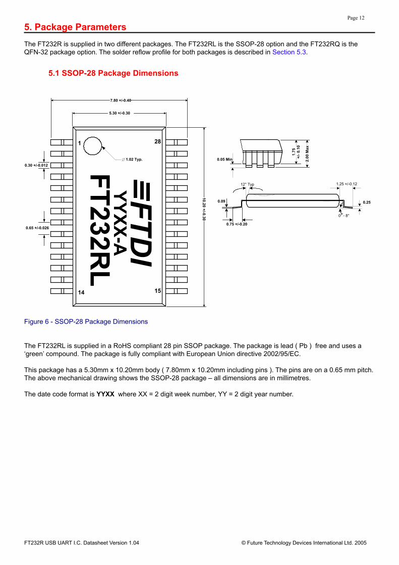
5.1 SSOP-28 Package Dimensions
12° Typ
0° - 8°
0.25
0.75 +/-0.20
0.09
2.00
Max
1.75
+/-
0.10
0.05 Min
1.25 +/-0.12
FT
232RL
YY
XX
-A
1
14 15
28
FT
DI
5.30 +/-0.30
7.80 +/-0.40
10.20 +/-0.30
1.02 Typ.
0.30 +/-0.012
0.65 +/-0.026
Figure 6 - SSOP-28 Package Dimensions
The FT232RL is supplied in a RoHS compliant 28 pin SSOP package. The package is lead ( Pb ) free and uses a ‘green’ compound. The package is fully compliant with European Union directive 2002/95/EC.
This package has a 5.30mm x 10.20mm body ( 7.80mm x 10.20mm including pins ). The pins are on a 0.65 mm pitch. The above mechanical drawing shows the SSOP-28 package – all dimensions are in millimetres.
The date code format is YYXX where XX = 2 digit week number, YY = 2 digit year number.
FT232R USB UART I.C. Datasheet Version 1.04 © Future Technology Devices International Ltd. 2005
Page 13
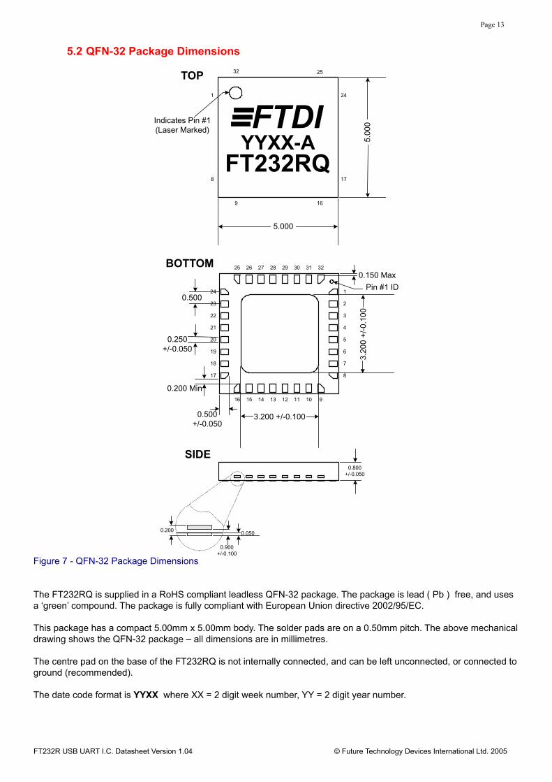
5.2 QFN-32 Package Dimensions
Figure 7 - QFN-32 Package Dimensions
The FT232RQ is supplied in a RoHS compliant leadless QFN-32 package. The package is lead ( Pb ) free, and uses a ‘green’ compound. The package is fully compliant with European Union directive 2002/95/EC.
This package has a compact 5.00mm x 5.00mm body. The solder pads are on a 0.50mm pitch. The above mechanical drawing shows the QFN-32 package – all dimensions are in millimetres.
The centre pad on the base of the FT232RQ is not internally connected, and can be left unconnected, or connected to ground (recommended).
The date code format is YYXX where XX = 2 digit week number, YY = 2 digit year number.
Indicates Pin #1 (Laser Marked)
FT232RQ
32 25
24
17
169
8
1
YYXX-AFTDI
5.00
0
5.000
18
9
1
2
3
4
5
6
7
8
10111213141516
17
19
20
21
22
23
24
25 26 27 28 29 30 31 32
3.20
0 +
/-0.
100
3.200 +/-0.100
0.500
0.250 +/-0.050
0.200 Min
0.500 +/-0.050
0.150 Max
Pin #1 ID
0.800 +/-0.050
0.200 0.050
0.900 +/-0.100
TOP
BOTTOM
SIDE
FT232R USB UART I.C. Datasheet Version 1.04 © Future Technology Devices International Ltd. 2005
Page 14
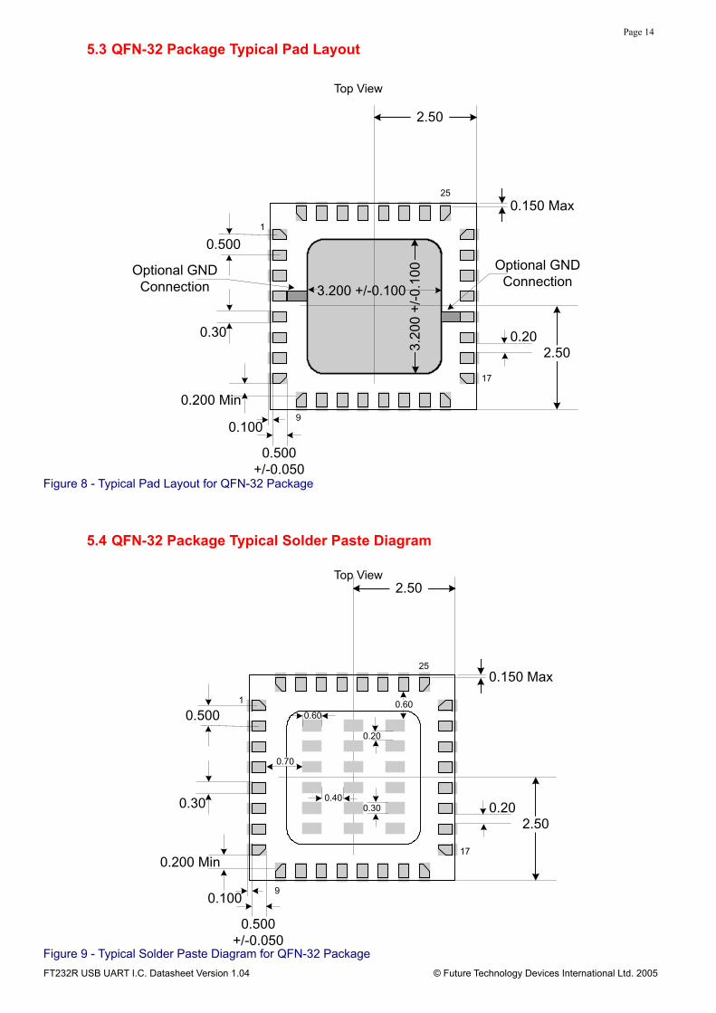
5.3 QFN-32 Package Typical Pad Layout
Top View
1
17
25
0.500
0.30
0.200 Min
0.500 +/-0.050
0.150 Max
0.20
0.1003.
200
+/-0
.100
3.200 +/-0.100
2.50
2.50
Optional GND Connection
Optional GND Connection
9
Figure 8 - Typical Pad Layout for QFN-32 Package
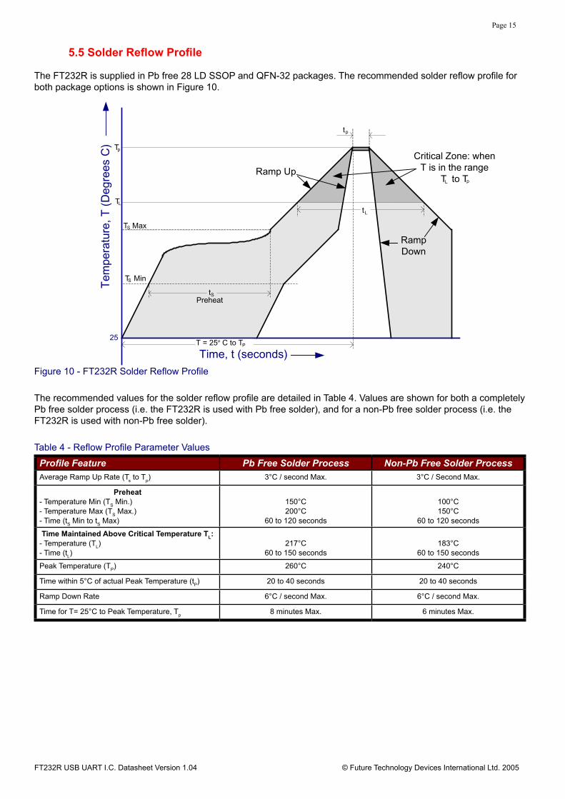
5.4 QFN-32 Package Typical Solder Paste Diagram
Top View
0.500
0.30
0.200 Min
0.500 +/-0.050
0.150 Max
0.20
0.100
2.50
2.50
0.20
0.30
0.60
0.40
0.70
0.601
17
25
9
Figure 9 - Typical Solder Paste Diagram for QFN-32 Package
FT232R USB UART I.C. Datasheet Version 1.04 © Future Technology Devices International Ltd. 2005
Page 15
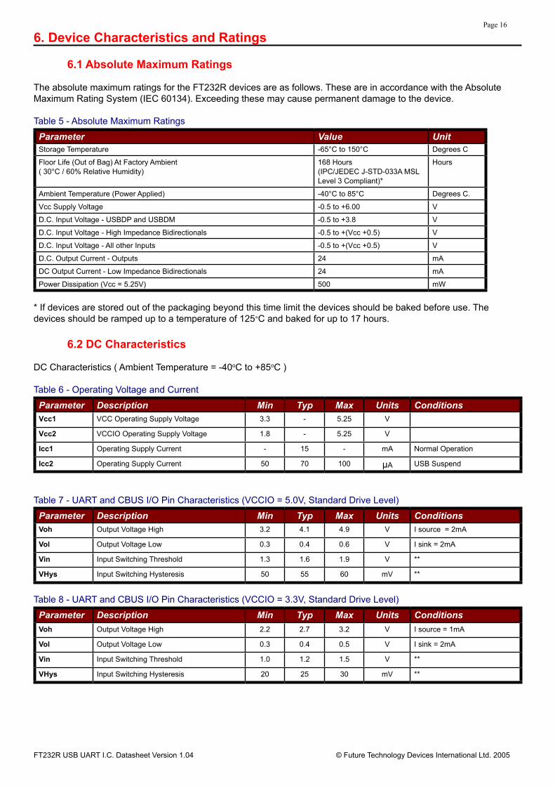
5.5 Solder Reflow Profile
Critical Zone: whenT is in the range
T to T
Tem
pera
ture
, T (
Deg
rees
C)
Time, t (seconds)
25PT = 25º C to T
tp
Tp
TL
tPreheat
S
tL
Ramp UpL p
RampDown
T MaxS
T MinS
Figure 10 - FT232R Solder Reflow Profile
The recommended values for the solder reflow profile are detailed in Table 4. Values are shown for both a completely Pb free solder process (i.e. the FT232R is used with Pb free solder), and for a non-Pb free solder process (i.e. the FT232R is used with non-Pb free solder).
Table 4 - Reflow Profile Parameter Values
Profile Feature Pb Free Solder Process Non-Pb Free Solder ProcessAverage Ramp Up Rate (Ts to Tp) 3°C / second Max. 3°C / Second Max.
Preheat- Temperature Min (TS Min.)- Temperature Max (TS Max.)- Time (tS Min to tS Max)
150°C200°C
60 to 120 seconds
100°C150°C
60 to 120 seconds
Time Maintained Above Critical Temperature TL:- Temperature (TL)- Time (tL)
217°C60 to 150 seconds
183°C60 to 150 seconds
Peak Temperature (TP) 260°C 240°C
Time within 5°C of actual Peak Temperature (tP) 20 to 40 seconds 20 to 40 seconds
Ramp Down Rate 6°C / second Max. 6°C / second Max.
Time for T= 25°C to Peak Temperature, Tp 8 minutes Max. 6 minutes Max.
The FT232R is supplied in Pb free 28 LD SSOP and QFN-32 packages. The recommended solder reflow profile for both package options is shown in Figure 10.
FT232R USB UART I.C. Datasheet Version 1.04 © Future Technology Devices International Ltd. 2005
Page 16
6. Device Characteristics and Ratings
6.1 Absolute Maximum Ratings
The absolute maximum ratings for the FT232R devices are as follows. These are in accordance with the Absolute Maximum Rating System (IEC 60134). Exceeding these may cause permanent damage to the device.
Table 5 - Absolute Maximum Ratings
Parameter Value UnitStorage Temperature -65°C to 150°C Degrees C
Floor Life (Out of Bag) At Factory Ambient( 30°C / 60% Relative Humidity)
168 Hours(IPC/JEDEC J-STD-033A MSL Level 3 Compliant)*
Hours
Ambient Temperature (Power Applied) -40°C to 85°C Degrees C.
Vcc Supply Voltage -0.5 to +6.00 V
D.C. Input Voltage - USBDP and USBDM -0.5 to +3.8 V
D.C. Input Voltage - High Impedance Bidirectionals -0.5 to +(Vcc +0.5) V
D.C. Input Voltage - All other Inputs -0.5 to +(Vcc +0.5) V
D.C. Output Current - Outputs 24 mA
DC Output Current - Low Impedance Bidirectionals 24 mA
Power Dissipation (Vcc = 5.25V) 500 mW
* If devices are stored out of the packaging beyond this time limit the devices should be baked before use. The devices should be ramped up to a temperature of 125°C and baked for up to 17 hours.
6.2 DC Characteristics
DC Characteristics ( Ambient Temperature = -40oC to +85oC )
Table 6 - Operating Voltage and Current
Parameter Description Min Typ Max Units ConditionsVcc1 VCC Operating Supply Voltage 3.3 - 5.25 V
Vcc2 VCCIO Operating Supply Voltage 1.8 - 5.25 V
Icc1 Operating Supply Current - 15 - mA Normal Operation
Icc2 Operating Supply Current 50 70 100 μA USB Suspend
Table 7 - UART and CBUS I/O Pin Characteristics (VCCIO = 5.0V, Standard Drive Level)
Parameter Description Min Typ Max Units ConditionsVoh Output Voltage High 3.2 4.1 4.9 V I source = 2mA
Vol Output Voltage Low 0.3 0.4 0.6 V I sink = 2mA
Vin Input Switching Threshold 1.3 1.6 1.9 V **
VHys Input Switching Hysteresis 50 55 60 mV **
Table 8 - UART and CBUS I/O Pin Characteristics (VCCIO = 3.3V, Standard Drive Level)
Parameter Description Min Typ Max Units ConditionsVoh Output Voltage High 2.2 2.7 3.2 V I source = 1mA
Vol Output Voltage Low 0.3 0.4 0.5 V I sink = 2mA
Vin Input Switching Threshold 1.0 1.2 1.5 V **
VHys Input Switching Hysteresis 20 25 30 mV **
FT232R USB UART I.C. Datasheet Version 1.04 © Future Technology Devices International Ltd. 2005
Page 17Table 9 - UART and CBUS I/O Pin Characteristics (VCCIO = 2.8V, Standard Drive Level)
Parameter Description Min Typ Max Units ConditionsVoh Output Voltage High 2.1 2.6 3.1 V I source = 1mA
Vol Output Voltage Low 0.3 0.4 0.5 V I sink = 2mA
Vin Input Switching Threshold 1.0 1.2 1.5 V **
VHys Input Switching Hysteresis 20 25 30 mV **
Table 10 - UART and CBUS I/O Pin Characteristics (VCCIO = 5.0V, High Drive Level)
Parameter Description Min Typ Max Units ConditionsVoh Output Voltage High 3.2 4.1 4.9 V I source = 6mA
Vol Output Voltage Low 0.3 0.4 0.6 V I sink = 6mA
Vin Input Switching Threshold 1.3 1.6 1.9 V **
VHys Input Switching Hysteresis 50 55 60 mV **
Table 11 - UART and CBUS I/O Pin Characteristics (VCCIO = 3.3V, High Drive Level)
Parameter Description Min Typ Max Units ConditionsVoh Output Voltage High 2.2 2.8 3.2 V I source = 3mA
Vol Output Voltage Low 0.3 0.4 0.6 V I sink = 8mA
Vin Input Switching Threshold 1.0 1.2 1.5 V **
VHys Input Switching Hysteresis 20 25 30 mV **
Table 12 - UART and CBUS I/O Pin Characteristics (VCCIO = 2.8V, High Drive Level)
Parameter Description Min Typ Max Units ConditionsVoh Output Voltage High 2.1 2.8 3.2 V I source = 3mA
Vol Output Voltage Low 0.3 0.4 0.6 V I sink = 8mA
Vin Input Switching Threshold 1.0 1.2 1.5 V **
VHys Input Switching Hysteresis 20 25 30 mV **
**Inputs have an internal 200kΩ pull-up resistor to VCCIO.
Table 13 - RESET# and TEST Pin Characteristics
Parameter Description Min Typ Max Units ConditionsVin Input Switching Threshold 1.3 1.6 1.9 V
VHys Input Switching Hysteresis 50 55 60 mV
Table 14 - USB I/O Pin (USBDP, USBDM) Characteristics
Parameter Description Min Typ Max Units ConditionsUVoh I/O Pins Static Output ( High) 2.8 3.6 V RI = 1.5kΩ to 3V3Out ( D+ )
RI = 15kΩ to GND ( D- )
UVol I/O Pins Static Output ( Low ) 0 0.3 V RI = 1.5kΩ to 3V3Out ( D+ ) RI = 15kΩ to GND ( D- )
UVse Single Ended Rx Threshold 0.8 2.0 V
UCom Differential Common Mode 0.8 2.5 V
UVDif Differential Input Sensitivity 0.2 V
UDrvZ Driver Output Impedance 26 29 44 Ohms ***
***Driver Output Impedance includes the internal USB series resistors on USBDP and USBDM pins.
FT232R USB UART I.C. Datasheet Version 1.04 © Future Technology Devices International Ltd. 2005
Page 18
6.3 EEPROM Reliability Characteristics
The internal 1024 Bit EEPROM has the following reliability characteristics-
Table 15 - EEPROM Characteristics
Parameter Description Value UnitData Retention 15 Years
Read / Write Cycles 100,000 Cycles
6.4 Internal Clock Characteristics
The internal Clock Oscillator has the following characteristics.
Table 16 - Internal Clock Characteristics
Parameter Value UnitMin Typical Max
Frequency of Operation 11.98 12.00 12.02 MHz****
Clock Period 83.19 83.33 83.47 ns
Duty Cycle 45 50 55 %
****Equivalent to +/-1667ppm.
Table 17 - OSCI, OSCO Pin Characteristics (Optional - Only applies if external Oscillator is used*****)
Parameter Description Min Typ Max Units ConditionsVoh Output Voltage High 2.8 - 3.6 V Fosc = 12MHz
Vol Output Voltage Low 0.1 - 1.0 V Fosc = 12MHz
Vin Input Switching Threshold 1.8 2.5 3.2 V
*****When supplied the device is configured to use its internal clock oscillator. Users who wish to use an external oscillator or crystal should contact FTDI technical support.
FT232R USB UART I.C. Datasheet Version 1.04 © Future Technology Devices International Ltd. 2005
Page 19
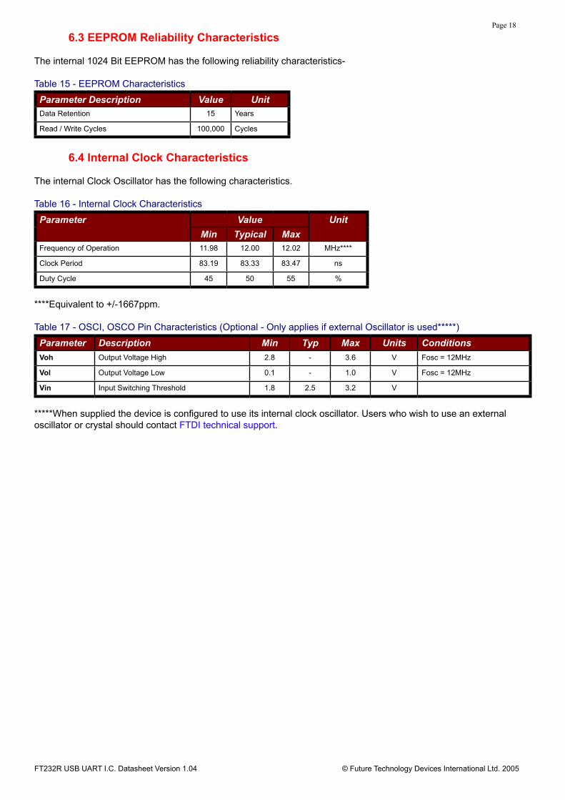
7. Device ConfigurationsPlease note that pin numbers on the FT232R chip in this section have deliberately been left out as they vary between the FT232RL and FT232RQ versions of the device. All of these configurations apply to both package options for the FT232R device. Please refer to Section 4 for the package option pin-out and signal descriptions.
7.1 Bus Powered Configuration
Figure 11 - Bus Powered Configuration
Figure 11 illustrates the FT232R in a typical USB bus powered design configuration. A USB Bus Powered device gets its power from the USB bus. Basic rules for USB Bus power devices are as follows –
i) On plug-in to USB, the device must draw no more than 100mA.
ii) On USB Suspend the device must draw no more than 500μA.
iii) A Bus Powered High Power USB Device (one that draws more than 100mA) should use one of the CBUS pins configured as PWREN# and use it to keep the current below 100mA on plug-in and 500μA on USB suspend.
iv) A device that consumes more than 100mA can not be plugged into a USB Bus Powered Hub.
v) No device can draw more that 500mA from the USB Bus.
The power descriptor in the internal EEPROM should be programmed to match the current draw of the device.A Ferrite Bead is connected in series with USB power to prevent noise from the device and associated circuitry (EMI) being radiated down the USB cable to the Host. The value of the Ferrite Bead depends on the total current required by the circuit – a suitable range of Ferrite Beads is available from Steward (www.steward.com) for example Steward Part # MI0805K400R-00.
FT232R
AGND
GND
GND
GND
TEST100nF
3V3OUT
VCCIO
NC
RESET#
NC
+100nF
10nF
Vcc
TXD
RXD
RTS#
CTS#
DTR#
DSR#
DCD#
RI#
CBUS0
CBUS3
CBUS2
CBUS1
USBDP
USBDM
VCC1
2
3
4
5
OSCI
OSCO
CBUS4
FerriteBead
+
4.7uF
SHIELD
GND
GND
GND
GND
Vcc
FT232R USB UART I.C. Datasheet Version 1.04 © Future Technology Devices International Ltd. 2005
Page 20
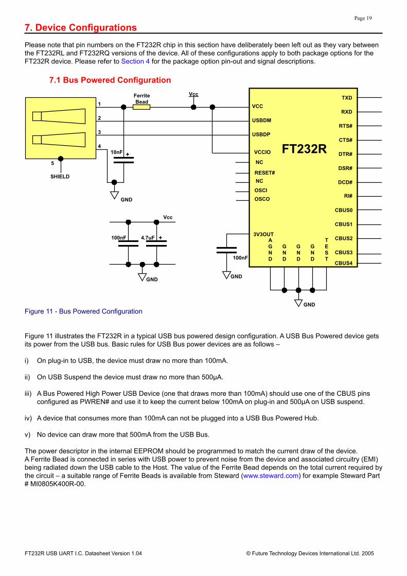
7.2 Self Powered Configuration
Figure 12 Self Powered Configuration
Figure 12 illustrates the FT232R in a typical USB self powered configuration. A USB Self Powered device gets its power from its own power supply and does not draw current from the USB bus. The basic rules for USB Self powered devices are as follows –
i) A Self Powered device should not force current down the USB bus when the USB Host or Hub Controller is powered down.
ii) A Self Powered Device can use as much current as it likes during normal operation and USB suspend as it has its own power supply.
iii) A Self Powered Device can be used with any USB Host and both Bus and Self Powered USB Hubs
The power descriptor in the internal EEPROM should be programmed to a value of zero (self powered).
In order to meet requirement (i) the USB Bus Power is used to control the RESET# Pin of the FT232R device. When the USB Host or Hub is powered up the internal 1.5kΩ resistor on USBDP is pulled up to 3.3V, thus identifying the device as a full speed device to USB. When the USB Host or Hub power is off, RESET# will go low and the device will be held in reset. As RESET# is low, the internal 1.5kΩ resistor will not be pulled up to 3.3V, so no current will be forced down USBDP via the 1.5kΩ pull-up resistor when the host or hub is powered down. Failure to do this may cause some USB host or hub controllers to power up erratically.
Figure 10 illustrates a self powered design which has a 3.3V - 5V supply. A design which is interfacing to 2.8V - 1.8V logic would have a 2.8V - 1.8V supply to VCCIO, and a 3.3V - 5V supply to VCC
Note : When the FT232R is in reset, the UART interface pins all go tri-state. These pins have internal 200kΩ pull-up resistors to VCCIO, so they will gently pull high unless driven by some external logic.
FT232R
AGND
GND
GND
GND
TEST100nF
3V3OUT
VCCIO
NC
RESET#
NC
+100nF
VCC
TXD
RXD
RTS#
CTS#
DTR#
DSR#
DCD#
RI#
CBUS0
CBUS3
CBUS2
CBUS1
USBDP
USBDM
VCC1
2
3
4
5
OSCI
OSCO
CBUS4
4.7uF
SHIELD
GND GND
GND
GND
VCC = 3.3V - 5V
GND
10k
4k7
100nF
FT232R USB UART I.C. Datasheet Version 1.04 © Future Technology Devices International Ltd. 2005
Page 21
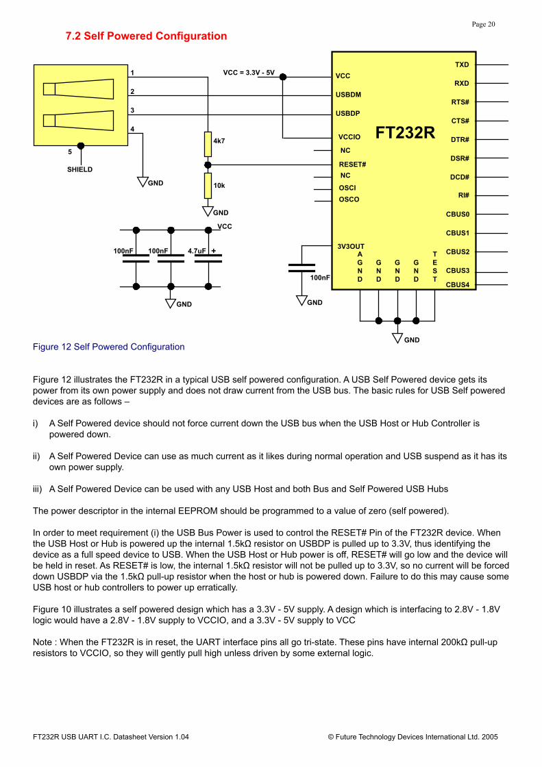
7.3 USB Bus Powered with Power Switching Configuration
Figure 13 - Bus Powered with Power Switching Configuration
USB Bus powered circuits need to be able to power down in USB suspend mode in order to meet the <= 500μA total USB suspend current requirement (including external logic). Some external logic can power itself down into a low current state by monitoring the PWREN# signal. For external logic that cannot power itself down in this way, the FT232R provides a simple but effective way of turning off power to external circuitry during USB suspend.
Figure 13 shows how to use a discrete P-Channel Logic Level MOSFET to control the power to external logic circuits. A suitable device would be an International Rectifier (www.irf.com) IRLML6402, or equivalent. It is recommended that a “soft start” circuit consisting of a 1kΩ series resistor and a 0.1μF capacitor are used to limit the current surge when the MOSFET turns on. Without the soft start circuit there is a danger that the transient power surge of the MOSFET turning on will reset the FT232R, or the USB host / hub controller. The values used here allow attached circuitry to power up with a slew rate of ~12.5V per millisecond, in other words the output voltage will transition from GND to 5V in approximately 400 microseconds.
Alternatively, a dedicated power switch I.C. with inbuilt “soft-start” can be used instead of a MOSFET. A suitable power switch I.C. for such an application would be a Micrel (www.micrel.com) MIC2025-2BM or equivalent.
Please note the following points in connection with power controlled designs –
i) The logic to be controlled must have its own reset circuitry so that it will automatically reset itself when power is re-applied on coming out of suspend.
ii) Set the Pull-down on Suspend option in the internal EEPROM.iii) One of the CBUS Pins should be configured as PWREN# in the internal EEPROM, and should be used to switch
the power supply to the external circuitry..iv) For USB high-power bus powered device (one that consumes greater than 100mA, and up to 500mA of current
from the USB bus), the power consumption of the device should be set in the max power field in the internal EEPROM. A high-power bus powered device must use this descriptor in the internal EEPROM to inform the system of its power requirements.
v) For 3.3V power controlled circuits the VCCIO pin must not be powered down with the external circuitry (the PWREN# signal gets its VCC supply from VCCIO). Either connect the power switch between the output of the 3.3V regulator and the external 3.3V logic or power VCCIO from the 3V3OUT pin of the FT232R.
FT232R
AGND
GND
GND
GND
TEST100nF
3V3OUT
VCCIO
NC
RESET#
NC
+100nF
10nF
5V VCC
TXD
RXD
RTS#
CTS#
DTR#
DSR#
DCD#
RI#
CBUS0
CBUS3
CBUS2
CBUS1
USBDP
USBDM
VCC1
2
3
4
5
OSCI
OSCO
CBUS4
FerriteBead
+
4.7uF
SHIELD
GND
GND
GND
GND
0.1uF 0.1uF
1k
Soft StartCircuit
d
g
s Switched 5V Powerto External Logic
5V VCC
P-Channel PowerMOSFET
PWREN#
FT232R USB UART I.C. Datasheet Version 1.04 © Future Technology Devices International Ltd. 2005
Page 22
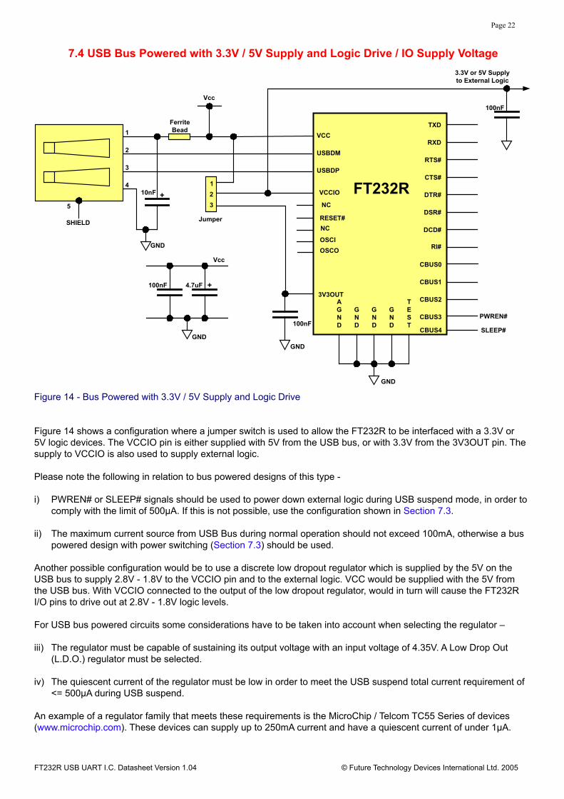
7.4 USB Bus Powered with 3.3V / 5V Supply and Logic Drive / IO Supply Voltage
Figure 14 - Bus Powered with 3.3V / 5V Supply and Logic Drive
Figure 14 shows a configuration where a jumper switch is used to allow the FT232R to be interfaced with a 3.3V or 5V logic devices. The VCCIO pin is either supplied with 5V from the USB bus, or with 3.3V from the 3V3OUT pin. The supply to VCCIO is also used to supply external logic.
Please note the following in relation to bus powered designs of this type -
i) PWREN# or SLEEP# signals should be used to power down external logic during USB suspend mode, in order to comply with the limit of 500μA. If this is not possible, use the configuration shown in Section 7.3.
ii) The maximum current source from USB Bus during normal operation should not exceed 100mA, otherwise a bus powered design with power switching (Section 7.3) should be used.
Another possible configuration would be to use a discrete low dropout regulator which is supplied by the 5V on the USB bus to supply 2.8V - 1.8V to the VCCIO pin and to the external logic. VCC would be supplied with the 5V from the USB bus. With VCCIO connected to the output of the low dropout regulator, would in turn will cause the FT232R I/O pins to drive out at 2.8V - 1.8V logic levels.
For USB bus powered circuits some considerations have to be taken into account when selecting the regulator –
iii) The regulator must be capable of sustaining its output voltage with an input voltage of 4.35V. A Low Drop Out (L.D.O.) regulator must be selected.
iv) The quiescent current of the regulator must be low in order to meet the USB suspend total current requirement of <= 500μA during USB suspend.
An example of a regulator family that meets these requirements is the MicroChip / Telcom TC55 Series of devices (www.microchip.com). These devices can supply up to 250mA current and have a quiescent current of under 1μA.
FT232R
AGND
GND
GND
GND
TEST100nF
3V3OUT
VCCIO
NC
RESET#
NC
10nF
TXD
RXD
RTS#
CTS#
DTR#
DSR#
DCD#
RI#
CBUS0
CBUS3
CBUS2
CBUS1
USBDP
USBDM
VCC1
2
3
4
5
OSCI
OSCO
CBUS4
FerriteBead
+
SHIELD
GND
GND
GND
3.3V or 5V Supplyto External Logic
100nF
+100nF
Vcc
4.7uF
GND
1
Jumper
SLEEP#
PWREN#
2
3
Vcc
FT232R USB UART I.C. Datasheet Version 1.04 © Future Technology Devices International Ltd. 2005
Page 23
8. Example Interface ConfigurationsAs in the Device Configurations section, please note that pin numbers on the FT232R chip in this section have deliberately been left out as they vary between the FT232RL and FT232RQ versions of the device. All of these configurations apply to both package options for the FT232R device. Please refer to Section 4 for the package option pin-out and signal descriptions.
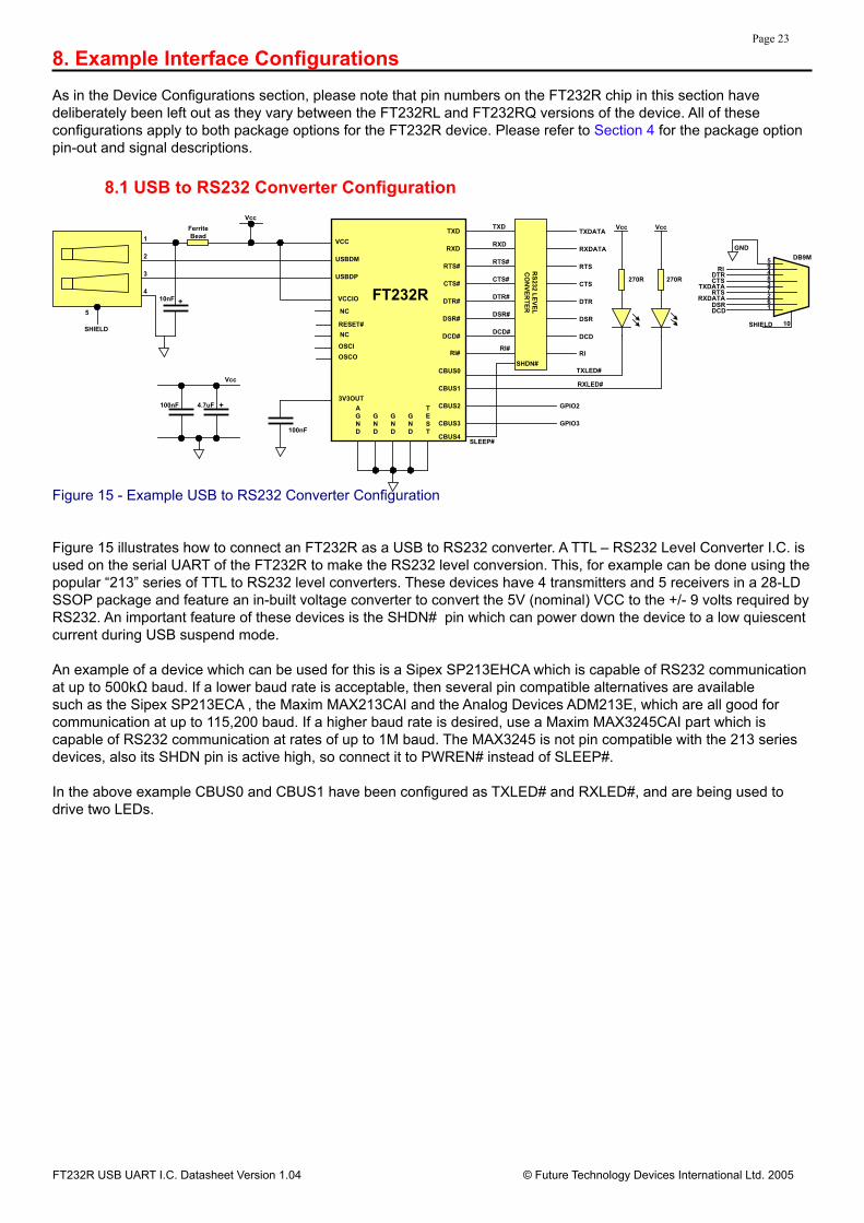
8.1 USB to RS232 Converter Configuration
Figure 15 - Example USB to RS232 Converter Configuration
Figure 15 illustrates how to connect an FT232R as a USB to RS232 converter. A TTL – RS232 Level Converter I.C. is used on the serial UART of the FT232R to make the RS232 level conversion. This, for example can be done using the popular “213” series of TTL to RS232 level converters. These devices have 4 transmitters and 5 receivers in a 28-LD SSOP package and feature an in-built voltage converter to convert the 5V (nominal) VCC to the +/- 9 volts required by RS232. An important feature of these devices is the SHDN# pin which can power down the device to a low quiescent current during USB suspend mode.
An example of a device which can be used for this is a Sipex SP213EHCA which is capable of RS232 communication at up to 500kΩ baud. If a lower baud rate is acceptable, then several pin compatible alternatives are available such as the Sipex SP213ECA , the Maxim MAX213CAI and the Analog Devices ADM213E, which are all good for communication at up to 115,200 baud. If a higher baud rate is desired, use a Maxim MAX3245CAI part which is capable of RS232 communication at rates of up to 1M baud. The MAX3245 is not pin compatible with the 213 series devices, also its SHDN pin is active high, so connect it to PWREN# instead of SLEEP#.
In the above example CBUS0 and CBUS1 have been configured as TXLED# and RXLED#, and are being used to drive two LEDs.
FT232R
AGND
GND
GND
GND
TEST100nF
3V3OUT
VCCIO
NC
RESET#
NC
+100nF
10nF
Vcc
TXD
RXD
RTS#
CTS#
DTR#
DSR#
DCD#
RI#
CBUS0
CBUS3
CBUS2
CBUS1
GPIO2
GPIO3
USBDP
USBDM
VCC1
2
3
4
5
OSCI
OSCO
CBUS4SLEEP#
FerriteBead
+
4.7uF
Vcc Vcc
270R270R
SHIELD
594837261
TXDATA
RXDATARTS
CTSDTR
DSRDCD
RI
SHIELD
GND
10
DB9M
RS
232 LE
VE
LC
ON
VE
RT
ER
TXDATA
RXDATA
RTS
CTS
DTR
DSR
DCD
RI
TXD
RXD
RTS#
CTS#
DTR#
DSR#
DCD#
RI#
TXLED#
RXLED#
SHDN#
Vcc
FT232R USB UART I.C. Datasheet Version 1.04 © Future Technology Devices International Ltd. 2005
Page 24
8.2 USB to RS485 Converter Configuration
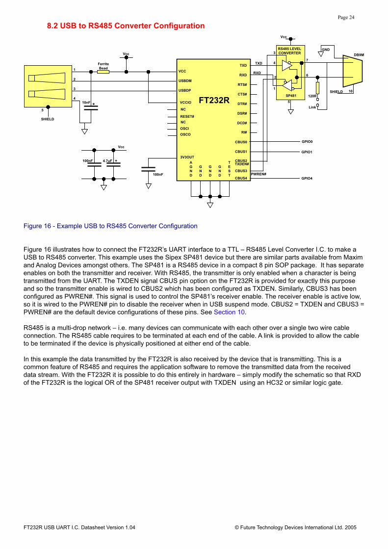
Figure 16 - Example USB to RS485 Converter Configuration
Figure 16 illustrates how to connect the FT232R’s UART interface to a TTL – RS485 Level Converter I.C. to make a USB to RS485 converter. This example uses the Sipex SP481 device but there are similar parts available from Maxim and Analog Devices amongst others. The SP481 is a RS485 device in a compact 8 pin SOP package. It has separate enables on both the transmitter and receiver. With RS485, the transmitter is only enabled when a character is being transmitted from the UART. The TXDEN signal CBUS pin option on the FT232R is provided for exactly this purpose and so the transmitter enable is wired to CBUS2 which has been configured as TXDEN. Similarly, CBUS3 has been configured as PWREN#. This signal is used to control the SP481’s receiver enable. The receiver enable is active low, so it is wired to the PWREN# pin to disable the receiver when in USB suspend mode. CBUS2 = TXDEN and CBUS3 = PWREN# are the default device configurations of these pins. See Section 10.
RS485 is a multi-drop network – i.e. many devices can communicate with each other over a single two wire cable connection. The RS485 cable requires to be terminated at each end of the cable. A link is provided to allow the cable to be terminated if the device is physically positioned at either end of the cable.
In this example the data transmitted by the FT232R is also received by the device that is transmitting. This is a common feature of RS485 and requires the application software to remove the transmitted data from the received data stream. With the FT232R it is possible to do this entirely in hardware – simply modify the schematic so that RXD of the FT232R is the logical OR of the SP481 receiver output with TXDEN using an HC32 or similar logic gate.
FT232R
AGND
GND
GND
GND
TEST100nF
3V3OUT
VCCIO
NC
RESET#
NC
+100nF
10nF
Vcc
TXD
RXD
RTS#
CTS#
DTR#
DSR#
DCD#
RI#
CBUS0
CBUS3
CBUS2
CBUS1 GPIO1
GPIO4
USBDP
USBDM
VCC1
2
3
4
5
OSCI
OSCO
CBUS4
TXDEN#
FerriteBead
+
4.7uF
SHIELD
SHIELD
GND
10
DB9M
RS485 LEVELCONVERTER
TXD
RXD
PWREN#
Vcc
Link
120R
5
6
7
3
4
1
2
SP481
GPIO0
Vcc
FT232R USB UART I.C. Datasheet Version 1.04 © Future Technology Devices International Ltd. 2005
Page 25
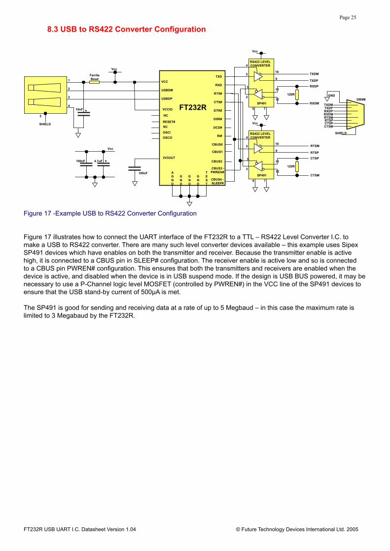
8.3 USB to RS422 Converter Configuration
FT232R
100nF
3V3OUT
VCCIO
NC
RESET#
NC
+100nF
10nF
Vcc
TXD
RXD
RTS#
CTS#
DTR#
DSR#
DCD#
RI#
CBUS0
CBUS3 -PWREN#
CBUS2
CBUS1
USBDP
USBDM
VCC1
2
3
4
5
OSCI
OSCO
CBUS4 -SLEEP#
FerriteBead
+
4.7uF
SHIELD
RS422 LEVELCONVERTER
Vcc
120R
6
9
10
4
5
2
3
SP491
11
12
7
RS422 LEVELCONVERTER
Vcc
120R
6
9
10
4
5
2
3
SP491
11
12
7
TXDM
TXDP
RXDP
RXDM
RTSM
RTSP
CTSP
CTSMAGND
GND
GND
GND
TEST
SHIELD
GNDDB9M
TXDMTXDPRXDPRXDMRTSMRTSPCTSPCTSM
Vcc
Figure 17 -Example USB to RS422 Converter Configuration
Figure 17 illustrates how to connect the UART interface of the FT232R to a TTL – RS422 Level Converter I.C. to make a USB to RS422 converter. There are many such level converter devices available – this example uses Sipex SP491 devices which have enables on both the transmitter and receiver. Because the transmitter enable is active high, it is connected to a CBUS pin in SLEEP# configuration. The receiver enable is active low and so is connected to a CBUS pin PWREN# configuration. This ensures that both the transmitters and receivers are enabled when the device is active, and disabled when the device is in USB suspend mode. If the design is USB BUS powered, it may be necessary to use a P-Channel logic level MOSFET (controlled by PWREN#) in the VCC line of the SP491 devices to ensure that the USB stand-by current of 500μA is met.
The SP491 is good for sending and receiving data at a rate of up to 5 Megbaud – in this case the maximum rate is limited to 3 Megabaud by the FT232R.
FT232R USB UART I.C. Datasheet Version 1.04 © Future Technology Devices International Ltd. 2005
Page 26
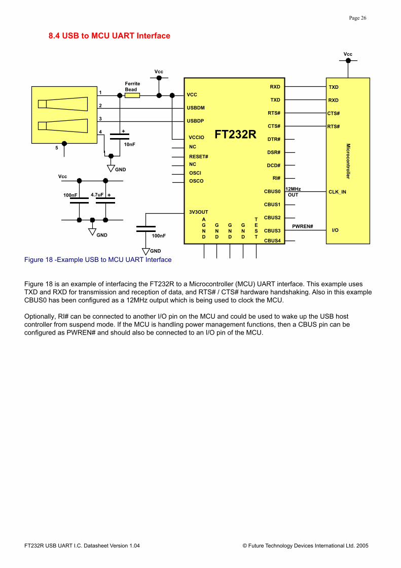
8.4 USB to MCU UART Interface
Figure 18 -Example USB to MCU UART Interface
Figure 18 is an example of interfacing the FT232R to a Microcontroller (MCU) UART interface. This example uses TXD and RXD for transmission and reception of data, and RTS# / CTS# hardware handshaking. Also in this example CBUS0 has been configured as a 12MHz output which is being used to clock the MCU.
Optionally, RI# can be connected to another I/O pin on the MCU and could be used to wake up the USB host controller from suspend mode. If the MCU is handling power management functions, then a CBUS pin can be configured as PWREN# and should also be connected to an I/O pin of the MCU.
FT232R
AGND
GND
GND
GND
TEST100nF
3V3OUT
VCCIO
NC
RESET#
NC
+100nF 4.7uF
Vcc
RXD
TXD
RTS#
CTS#
DTR#
DSR#
DCD#
RI#
CBUS0
CBUS3
CBUS2
CBUS1
USBDP
USBDM
VCC1
2
3
4
5
OSCI
OSCO
CBUS4
PWREN#
Micro
con
troller
TXD
RXD
CTS#
RTS#
CLK_IN
I/O
FerriteBead
GND
GND
GND
+
GND
10nF
12MHzOUT
Vcc
Vcc
FT232R USB UART I.C. Datasheet Version 1.04 © Future Technology Devices International Ltd. 2005
Page 27
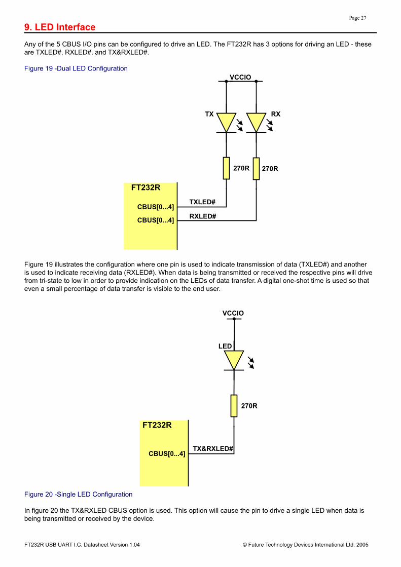
9. LED InterfaceAny of the 5 CBUS I/O pins can be configured to drive an LED. The FT232R has 3 options for driving an LED - these are TXLED#, RXLED#, and TX&RXLED#.
Figure 19 -Dual LED Configuration
TXLED#
RXLED#CBUS[0...4]
CBUS[0...4]
VCCIO
270R 270R
TX RX
FT232R
TX&RXLED#CBUS[0...4]
VCCIO
270R
LED
FT232R
Figure 19 illustrates the configuration where one pin is used to indicate transmission of data (TXLED#) and another is used to indicate receiving data (RXLED#). When data is being transmitted or received the respective pins will drive from tri-state to low in order to provide indication on the LEDs of data transfer. A digital one-shot time is used so that even a small percentage of data transfer is visible to the end user.
Figure 20 -Single LED Configuration
In figure 20 the TX&RXLED CBUS option is used. This option will cause the pin to drive a single LED when data is being transmitted or received by the device.
FT232R USB UART I.C. Datasheet Version 1.04 © Future Technology Devices International Ltd. 2005
Page 28
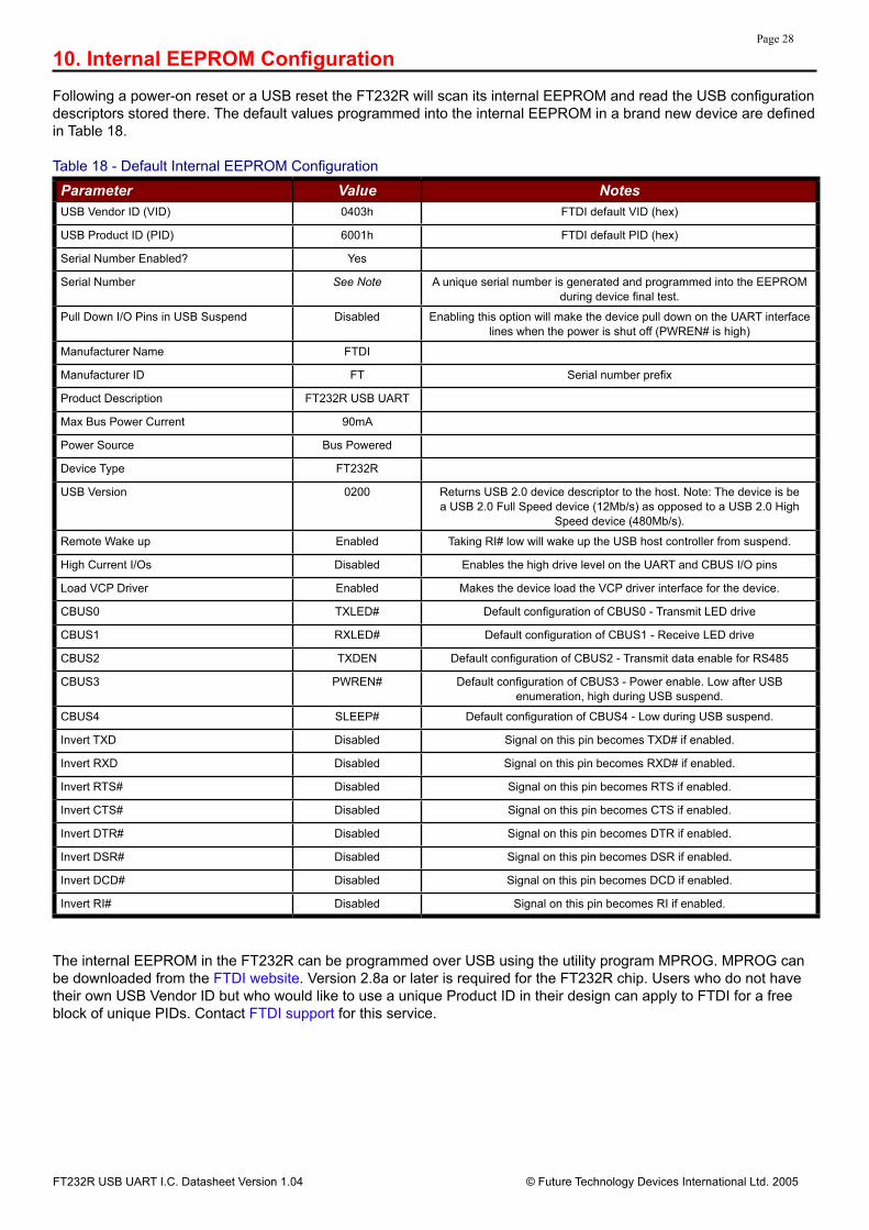
10. Internal EEPROM ConfigurationFollowing a power-on reset or a USB reset the FT232R will scan its internal EEPROM and read the USB configuration descriptors stored there. The default values programmed into the internal EEPROM in a brand new device are defined in Table 18.
Table 18 - Default Internal EEPROM Configuration
Parameter Value NotesUSB Vendor ID (VID) 0403h FTDI default VID (hex)
USB Product ID (PID) 6001h FTDI default PID (hex)
Serial Number Enabled? Yes
Serial Number See Note A unique serial number is generated and programmed into the EEPROM during device final test.
Pull Down I/O Pins in USB Suspend Disabled Enabling this option will make the device pull down on the UART interface lines when the power is shut off (PWREN# is high)
Manufacturer Name FTDI
Manufacturer ID FT Serial number prefix
Product Description FT232R USB UART
Max Bus Power Current 90mA
Power Source Bus Powered
Device Type FT232R
USB Version 0200 Returns USB 2.0 device descriptor to the host. Note: The device is be a USB 2.0 Full Speed device (12Mb/s) as opposed to a USB 2.0 High
Speed device (480Mb/s).
Remote Wake up Enabled Taking RI# low will wake up the USB host controller from suspend.
High Current I/Os Disabled Enables the high drive level on the UART and CBUS I/O pins
Load VCP Driver Enabled Makes the device load the VCP driver interface for the device.
CBUS0 TXLED# Default configuration of CBUS0 - Transmit LED drive
CBUS1 RXLED# Default configuration of CBUS1 - Receive LED drive
CBUS2 TXDEN Default configuration of CBUS2 - Transmit data enable for RS485
CBUS3 PWREN# Default configuration of CBUS3 - Power enable. Low after USB enumeration, high during USB suspend.
CBUS4 SLEEP# Default configuration of CBUS4 - Low during USB suspend.
Invert TXD Disabled Signal on this pin becomes TXD# if enabled.
Invert RXD Disabled Signal on this pin becomes RXD# if enabled.
Invert RTS# Disabled Signal on this pin becomes RTS if enabled.
Invert CTS# Disabled Signal on this pin becomes CTS if enabled.
Invert DTR# Disabled Signal on this pin becomes DTR if enabled.
Invert DSR# Disabled Signal on this pin becomes DSR if enabled.
Invert DCD# Disabled Signal on this pin becomes DCD if enabled.
Invert RI# Disabled Signal on this pin becomes RI if enabled.
The internal EEPROM in the FT232R can be programmed over USB using the utility program MPROG. MPROG can be downloaded from the FTDI website. Version 2.8a or later is required for the FT232R chip. Users who do not have their own USB Vendor ID but who would like to use a unique Product ID in their design can apply to FTDI for a free block of unique PIDs. Contact FTDI support for this service.
FT232R USB UART I.C. Datasheet Version 1.04 © Future Technology Devices International Ltd. 2005
Page 29
Disclaimer
Copyright © Future Technology Devices International Limited , 2005.
Version 0.90 - Initial Datasheet Created August 2005Version 0.96 - Revised Pre-release datasheet October 2005Version 1.00 - Full datasheet released December 2005Version 1.02 - Minor revisions to datasheet 7th December 2005Version 1.03 - 9th January 2006 - Manufacturer ID added to default EEPROM configuration; Buffer sizes added.Version 1.04 - 30th January 2006 - QFN-32 Pad layout and solder paste diagrams added.
Neither the whole nor any part of the information contained in, or the product described in this manual, may be adapted or reproduced in any material or electronic form without the prior written consent of the copyright holder.
This product and its documentation are supplied on an as-is basis and no warranty as to their suitability for any particular purpose is either made or implied.
Future Technology Devices International Ltd. will not accept any claim for damages howsoever arising as a result of use or failure of this product. Your statutory rights are not affected.
This product or any variant of it is not intended for use in any medical appliance, device or system in which the failure of the product might reasonably be expected to result in personal injury.
This document provides preliminary information that may be subject to change without notice.
Contact FTDI
Head Office - Future Technology Devices International Ltd.373 Scotland Street,Glasgow G5 8QB,United Kingdom
Tel. : +(44) 141 429 2777Fax. : +(44) 141 429 2758
E-Mail (Sales) : [email protected] (Support) : [email protected] (General Enquiries) : [email protected]
Regional Sales Offices -
Future Technology Devices International Ltd. (Taiwan)4F, No 16-1,Sec. 6 Mincyuan East Road,Neihu District,Taipei 114,Taiwan, R.o.C.
Tel.: +886 2 8791 3570Fax: +886 2 8791 3576
E-Mail (Sales): [email protected] (Support): [email protected] (General Enquiries): [email protected]
Future Technology Devices International Ltd.(USA)5285 NE Elam Young Parkway, Suite B800Hillsboro,OR 97124-6499USA
Tel.: +1 (503) 547-0988Fax: +1 (503) 547-0987
E-Mail (Sales): [email protected] (Support): [email protected] (General Enquiries): [email protected]
Website URL : http://www.ftdichip.com

![Catalogue FLYBACK Equivalent - [PDF Document] FLYBACK Equivalent FlyBack Equivalent flyback reemplazo conversor Flyback tv fly-back Flyback Tester Flyback Converter conversor Flyback](https://img.pdfslide.us/doc/110x75/5a832a447f8b9a9d308e9416/catalogue-flyback-equivalent-pdf-document-flyback-equivalent-flyback-equivalent.jpg)