Embed Size (px)
Citation preview

HAL Id: hal-00613279https://hal.archives-ouvertes.fr/hal-00613279
Submitted on 4 Aug 2011
HAL is a multi-disciplinary open accessarchive for the deposit and dissemination of sci-entific research documents, whether they are pub-lished or not. The documents may come fromteaching and research institutions in France orabroad, or from public or private research centers.
L’archive ouverte pluridisciplinaire HAL, estdestinée au dépôt et à la diffusion de documentsscientifiques de niveau recherche, publiés ou non,émanant des établissements d’enseignement et derecherche français ou étrangers, des laboratoirespublics ou privés.
Controlling roughness: from etching to nanotexturingand plasma-directed organization on organic and
inorganic materialsEvangelos Gogolides, Angeliki Tserepi, Vassilios Constantoudis, George
Kokkoris, Dimitrios Kontziampasis, Katerina Tsougeni, George Boulousis,Marilena Vlachopoulou
To cite this version:Evangelos Gogolides, Angeliki Tserepi, Vassilios Constantoudis, George Kokkoris, Dimitrios Kontzi-ampasis, et al.. Controlling roughness: from etching to nanotexturing and plasma-directed organi-zation on organic and inorganic materials. Journal of Physics D: Applied Physics, IOP Publishing,2011, 44 (17), pp.174021. �10.1088/0022-3727/44/17/174021�. �hal-00613279�

Controlling roughness: From etching to nanotexturing and plasma directedorganization on organic and inorganic materials
Evangelos Gogolides∗ , Angeliki Tserepi, Vassilios Constantoudis, George Kokkoris,Dimitrios Kontziampasis, Katerina Tsougeni, George Boulousis, Marilena VlachopoulouInstitute of Microelectronics, NCSR “Demokritos”, Terma Patriarhou Gregoriou St. AghiaParaskevi, Attiki, Greece 15310
AbstractWe describe how plasma-wall interactions in etching plasmas lead to either randomroughening / nanotexturing of polymeric and Silicon surfaces, or formation of organizednanostructures on such surfaces. We conduct carefully designed experiments of plasma-wallinteractions to understand the causes of both phenomena, and present Monte-Carlo simulationresults confirming the experiments. We discuss emerging applications in wetting and opticalproperty control, protein adsorption, microfluidics and lab-on-a-chip fabrication andmodification, and cost-effective silicon mold fabrication. We conclude with an outlook on theplasma reactor future designs to take advantage of the observed phenomena for new microand nanomanufacturing processes.
1. Introduction
Lithography followed by plasma etching is the main top-down approach for microand nanopatterning. Usually, during plasma etching ions “enhance” the removal of matter byneutrals and induce etch anisotropy (i.e. etching proceeds only towards the direction ofimpinging ions, which are accelerated perpendicularly to the substrate). However,microelectronic material etching has suffered for years from the so-called “grass” formed onplasma etched surfaces: The existence of any unetchable residues on the surface (or inside thematerial being etched) and the etch anisotropy lead to columnar nanostructure formation(grass), the column being protected by the unetchable material. Scanning-electron-microscope (SEM) images of grass among structures are standard textbook material ofetching problems in microelectronics fabrication classes.
On the other hand, grass may be seen as simply nanoroughness, or as desirednanotexture of a surface to be exploited for several applications. For example, if such a roughsurface is coated with a low-surface-energy-film an increase in hydrophobicity will beobserved leading to dramatic increases of the contact angle of water and oils (1) (2), (3), andeventually to a surface on which liquids roll, thus permitting self-cleaning action (4), (5) (6) of the surface. Another example where nanotexture is beneficial is when antireflectivity isdesired: Etch-induced nanoroughness is known to reduce reflectivity for both Si (the “blackSilicon” being a well known example (7)) and polymers for which the so called “nano-motheye” plasma roughening has been proposed (8). In fact for polymers plasmananotexturing can simultaneously achieve optical transparency, antireflectivity andsuperhydrophobicity (1, 9) . We would therefore like to emphasize that contrary to theundesirable effects of “grass” for nanoelectronics, controlled nanotexture formation may bevaluable for nanomanufacturing of both large areas as well as devices, when one or more“smart” functionalities may be desired (10) . As the Greeks would say “there is no bad thingwithout a good side-effect”, in other words one should not always cut the grass but rathercontrol its growth.
Despite the fact that during plasma nanotexturing one is removing material, the resultis the formation of grass-like nanostructures on the etched surface. This implies that plasmasmay be used for the assembly of nanostructures even when used in the “subtractive-etchingmode”. The subtractive mode has been used to create nano-grass on polymers (1) (2), (3), toform nanocolums after random deposition of metallic etch inhibitors on the surface andsubsequent etching (11), and recently to create Silicon nanotips and silicon nano-grass inHydrogen /Argon mixtures(12, 13). Using the “additive mode” on the other hand, several
Confidential: not for distribution. Submitted to IOP Publishing for peer review 8 November 2010

groups have also demonstrated assembly of random nanostructures from depositing plasmas.In fact silicon and other inorganic material nano-grass growth by plasmas is a very activefield as evidenced by several publications (14), (15), (16-18) including a recent review (19).Plasma has thus been proven to direct the assembly of both inorganic nanostructures(20),(19), and organic nanostructures (1),(2), while it has been claimed that plasmananofabrication mimics nature in the creation of the cosmos (21). Thus, additive orsubtractive plasma directed assembly emerges as a new field, under the broad title plasmananoscience.
However, in all the above plasma directed assembly efforts pattern order andperiodicity have not been looked at in detail or are missing as random patterns are formed. Anexception to this rule has been the organization of parallel ripples on stressed or lithographedpoly(dimethyl)siloxane (PDMS) films (22),(23) upon plasma oxidation. However, theformation of organized structures is often more desirable than random ones. For example,fabrication of organized, periodic nanodot, nanocolumn or nanopore arrays on surfaces isextremely useful in many fields ranging from biology, to hard disk drives, and from catalysisto photonics. Typically such structures are made with: a) either expensive nano-lithography(such as immersion, electron beam, Extreme Ultra Violet, or nanoimprint lithography)followed by smooth anisotropic plasma etching, b) self-assembly processes using blockcopolymers or colloidal nanospheres (24-27), which define an organized pattern usually on anintermediate polymeric layer, subsequently transferred to the substrate with smooth,anisotropic plasma etching (21, 27).
Very recently we have demonstrated that plasma etching alone can be used forplasma directed organization to BOTH create the organized nanodot pattern on any non-specialty commercial polymer, and then transfer it to the substrate (28) (29) . This finding haspromoted plasma etching, an inherently top-down technology also as a bottom-upnanomanufacturing tool. The duality of plasma etching (i.e. create and transfer the pattern) isindeed unique, and may change the way we have been doing nanofabrication. Additionally ithas added the dimension of plasma directed organization in the plasma nanoscience toolbox.To our knowledge only ion beam etching has up to now led to ion-beam directedorganization, as nicely reviewed in several recent papers (30-32). It is the authors’ opinionthat despite the “cleaner” environment of ion beams, plasmas offer more opportunities andmechanisms due to chemical and physical synergies, and are inherently more cost-effective.Thus, plasma directed assembly and plasma directed organization are very promisingemerging fields with a wealth of applications, modes (additive or subtractive), and materialsto act upon.
It is the purpose of this progress and perspective paper to focus on plasmananotexturing and plasma directed organization using mainly etching chemistries, i.e. asubtractive approach. This is to be complemented by the approaches of other groups whichuse mainly additive processes (19). We would like to encourage however our colleaguesusing depositing plasmas to look into the issue of nanostructure organization, as conditionsmay exist, where order is achieved. We believe that the phenomena we describe are generic,despite the fact that they are applied mostly for etching plasmas. Our approach in assemblingnanostructures is twofold: either to do so, on a surface from which material is removed, thusensuring that the nanostructures are of the same nature as the surface being etched, or to use asacrificial soft (usually polymer layer) for the nanostructure assembly, and then transfer thepattern to an underlying substrate. Crucial for all the above is the plasma-wall interaction andthis will be the focus of this paper.
Before moving on it is good to clarify some terminology. We have been using theterms plasma nanoroughening, plasma nanotexturing, and plasma directed assembly with nodifference to denote random nanostructure creation, although nanotexturing could be usedmore appropriately for soft materials, and plasma directed assembly is a rather broader terminitially used for depositing plasmas. To refer to organized structure formation we will beusing the term plasma directed organization or simply plasma organization.
2. What is different in plasma nanotexturing and plasma organization?

In the subtractive mode of patterning the main action is removal of material usingtypically plasma etching of selected areas of a substrate. While the main action is etching, avery small amount of co-deposition is also taking place. In general co-deposition is so smallthat it goes by unnoticed in most plasma etching processes. This co-deposition may typicallycome from sputtering of unetchable materials from the metallic or dielectric reactor wall (wecall these “hard” etch inhibitors(33)), from depositing material from the gas phase species, orfrom etchable wall materials (we call these “soft” inhibitors(33)) as shown schematically infigure 1. Normally all such co-depositing species would cause some type of “grass” formationafter prolonged etching, if some etch anisotropy is present. As we have shown, such co-deposition may lead to the so called roughness instability, i.e. almost linear increase ofroughness with time (33). However, the role of the etch inhibitors is not limited to theroughness instability. Experimental results (29) show that ordered periodic morphologies canbe induced on plasma etched polymeric surfaces. Thus, what is different in plasma directedassembly and organization is that the control of the ratios of ions/neutrals/inhibitors as well asthe selectivities and etching yields allows control of the order, the height, and the spacing ofthe formed nanostructures.
Several recent studies address the problem of plasma roughening of polymers and itsgrowth kinetics and most of them attempt its minimization in order to produce smooth etchingfor the nanoscale (34). However, rather than trying to suppress the appearance of plasmainstability we have been allowing its formation in order to use it for several applications aswill be discussed below, especially by tuning the geometry and the order of the assemblednanostructures (10).
Figure 1. Two mechanisms(33) for plasmananotexturing and roughness instability (i.e.linear growth of roughness with time). Thearrows indicate the angular distribution ofimpinging species. a) Mechanism with“hard” inhibitors coming from reactorwalls or electrode: The ratio of ions toinhibitors is higher in the valleys than onthe hills, due to more intense shadowing ofinhibitors compared to the ions. b)Mechanism with “soft” inhibitors: Theratio of reactive neutral species toinhibitors is higher in the valleys than onthe hills, due to the lower stickingprobability of reactive neutral species (SRN
< SSINH).
3. Plasma Nanotexturing and the role of reactor walls
We begin with a brief description of what plasma nanotexturing actually is. When a polymersurface is etched and a few microns of material have been removed, nanotexture may developon its surface, and roughness may increase linearly with time. This is shown in figure 2a fortwo organic polymers Poly(methyl methacrylate) PMMA, and Poly(ether ether ketone)PEEK. Starting from a flat surface, within minutes one can get a rough surface, and finally aporous rough layer. X ray photoelectron Spectroscopy (XPS) analysis shown in figure 2b,reveals relatively large surface concentration of Aluminum present in Oxide form (35)coming from sputtering of the Alumina dielectric dome, and the anodized Aluminum

clamping ring of the etch tool. This “hard” etch inhibitor creates micromasking and leads tothe development of nanotexture. In nanoscience terminology the plasma directs the assemblyof a rough nanotexture on the top surface of the polymer.
Figure 2. (a) Column Height on Micro and Nanotextured PMMA and PEEK plates in Helicon PlasmaReactor with Oxygen Plasma. The SEM images are shown embedded for selected times to reveal theporous surface formed. (b) Elemental XPS analysis of 0.5mm thick PMMA plate versus etching time.Notice the large surface concentration of Aluminum. The reactor dome was made from alumina (35).
The XPS results suggest that nanotexture is a result of plasma-wall interactions. We thusdecided to study how the phenomenon may be controlled by changing reactor wall material,and plasma reactor design. In this section we compare for the first time 7 different reactorwall conditions and their effects on the morphology of 3 representative materials, namelyPMMA-a typical organic polymer-, PDMS-a typical inorganic polymer-, and Silicon-a typicalinorganic material. Five out of the seven reactor conditions refer to different wall conditionsof one reactor type, namely the MET system by Adixen-Alcatel. The two remainingconditions refer to an ICP etcher developed by Oxford Plasma Technology (OIPT).
The Adixen reactor is a helicon type reactor with an antenna of one loop around adielectric (alumina) dome. The etching conditions in the Adixen tool were:
a) PMMA etch: -100 V bias, 10oC, 0.75 Pa, 1900 W, 100 sccm O2, PMMA etch rate1000 nm/min (for plates), 1659 nm/min (for films).
b) PDMS etch: -100 V bias, 15oC, 1.33 Pa, 1900 W, 200 sccm SF6 ,PDMS etch rate0.75µm/min
c) Si etch: - 55 V bias, 15oC, 5.25 Pa, 1800 W, 172 sccm SF6, Silicon etch rate5µm/min. The conditions were chosen to be identical to the etching step of the gaschopping (“Bosch”) process.
The OIPT reactor is an ICP with alumina dome having dielectric shielding, and a quartzclamping ring. The etching conditions in the OIPT reactor are described below and werechosen so as to achieve similar etching rates with the Adixen tool:
a) PMMA etch: -105 V bias, 5 oC, 0.74 Pa, 1000 W, 50 sccm O2, PMMA etch rate1194nm/min for films
b) PDMS etch: -100 V bias, 15 oC, , 1000 W, 200 sccm SF6, PDMS etch rate 0.7µm/minc) Si etch: - 55 V bias, 5 oC, 5 Pa, 1800 W, 172 sccm SF6, Si etch rate 10µm/min
The 7 wall conditions were the following:• Wall condition 1 (Alumina dome, Anodized Al ring, Helicon source) briefly
referred to as (Alumina, Anodized Al, Helicon) refers to clean alumina dome andanodized aluminum clamping ring of the Adixen Helicon System.
• Wall condition 2 (Polymer, Polymer, Helicon) refers to covering (painting with abrush) the interior of the dome of the Adixen Helicon System with photoresistpolymer, (especially in the area of high RF fields close to the antenna), and painting

the anodized aluminum ring also with photoresist (see figure 3a). Both surfaces werebaked after being painted with photoresist polymer.
• Wall condition 3 (Polymer, Anodized Al, Helicon), refers to painting only the domearea and NOT the anodized aluminum ring of the Adixen Helicon System (see figure3a).
• Wall condition 4 (Alumina, Polymer, Helicon), refers to painting only the anodizedaluminum ring and not the reactor dome of the Adixen Helicon System (see figure3a).
• Wall condition 5 (Quartz, Al, Helicon), refers to using an identical Adixen HeliconSystem with quartz dome and aluminum ring (not anodized).
• Wall condition 6 (Alumina, Quartz, ICP, Shield), refers to using an ICP reactorfrom OIPT, with quartz dome, and quartz ring, and having electrostatic shielding ofthe RF fields to minimize dome material sputtering.
• Wall condition 7 (Alumina, Quartz, ICP, No Shield), refers to using an ICP reactorfrom OIPT without electrostatic shielding of the RF dome.
Figure 3 shows several characteristic results from the 7 conditions used for the etching ofPMMA plates. Figure 3b shows an SEM picture of a PMMA film etched for 2 min in thehelicon reactor (etch depth 3.4µm). A columnar morphology is clearly seen on the film afteretching. Figure 3c shows how the morphology is influenced by changing the dome materialfrom alumina to quartz; Instead of columns nanomounds are now observed with height valuesless (approximately half) than those of the nanocolumns shown in figure 3b, as AFMmeasurements reveal (see also Table 1). Similar results are observed not only for films, butalso for commercial PMMA plates, as shown in figure 3d,e,f. Indeed, after 1min of etching(more than 2µm of etched depth) severe micro and nanotexture appears on the surface of theplate and the root mean square (rms) roughness jumps to more than 40nm (figure 3d). Plasmaetching directs the assembly of “grass” like micro-nanocolumns on PMMA as a result ofAlumina sputtering and micromasking. Figure 3d is the AFM version of figure 3b but for aplate rather than a film and for only 1min etching. When painting the dome and ring of thereactor with a photoresist polymer, roughness is halved (figure 3e), and the morphology of theassembled nanostructures changes from grass-like to nanomounds, suggesting a transitionfrom hard inhibitors (sputtered Al compounds from the reactor walls) to soft inhibitors(sputtered/partially etched photoresist polymer from the covered reactor wall). We note thatthis change is not accompanied by any significant etch rate reduction. In the OIPT reactor, anetching system designed for minimized sputtering and equipped with electrostatic shielding,roughness is only 4.5 nm even after 2min of etching (figure 3f), i.e. is reduced by an order ofmagnitude, resulting in relatively smooth surfaces.

Figure 3. Plasma nanotexturing of PMMA in O2 and the role of reactor walls. For the complete set ofexperiments refer to Table I. The z axis shows the range of height values in each image.(a) Schematic of the MET Helicon reactor showing the positions of painting with photoresist polymer
the walls in order to reduce wall material sputtering.(b) Wall condition 1 for PMMA film etched for 2min. The SEM image shows the morphology of apolymer film and the roughness formed.(c) Wall condition 5 for PMMA film etched for 2min. Conditions are the same as in figure 3b, the maindifference being that the dielectric dome material is quartz rather than Alumina.(d) PMMA plate etching at condition 1: Alumina dome and clamping ring with anodized aluminum.Scan size: 10x10µm, Treatment time: 1 min Rms: 41.8nm.(e) PMMA plate etching at condition 2: Photoresist on the ring and in the dome (only the antennaarea). Treatment time: 1min, Scan size: 4x4 µm. Rms: 23.7 nm.(f) PMMA plate etching at condition 7, Without Electrostatic Shielding of the RF field of the antenna,Treatment time: 2min, Scan size: 4x4 µm. Rms: 4.5 nm.Note: AFM images were processed using the Software WSxM(36)
Figure 4 shows characteristic etching results of PDMS (an inorganic polymer) withSF6 plasma. In a reactor with alumina dome and ring, etching for just two minutes leads toroughness value of approximately 100nm (rms) as shown in figure 4a. After painting both thering and the dome with an organic polymer roughness drops by more than an order ofmagnitude to only 8.7nm (figure 4b). When only the dome is covered with a polymer, whilethe anodized aluminum ring is exposed to the plasma, roughness increases slightly, but stillremains at low values of 11.6nm. It is also extremely interesting to see that when changingthe dome from Alumina to quartz, which is etched by the SF6 plasma, roughness remains tolow levels. Thus for PDMS etching the main contributor for roughness formation is thesputtering of alumina (in the form of Aluminum oxyfluoride) from the dome to the sample, aresult also observed for Silicon etching by others (37).

Figure 4. Plasma Nanotexturing of PDMS in SF6 and the role of reactor walls. For the complete set ofexperiments refer to Table I. The z axis shows the range of height values in each image.(a) PDMS etching in SF6 for 2min at wall conditions 1, rms=98nm.(b) PDMS etching in SF6 for 2min at wall condition 2, rms=8.7nm.(c) PDMS etching in SF6 at wall condition 3, rms=11.6nm.(d) PDMS etching in SF6 at wall condition 5 rms=11.2nm.
Finally experiments were done also for an inorganic material (Silicon) which isetched mostly isotropically and for which grass formation is not justified on the grounds ofanisotropy. Figure 5a shows that after etching silicon in SF6 plasma for 4 min (20µm etchdepth) rough nanomounds appear (38) with rms value of 9.3nm. When the dome and ring arecovered with photoresist, roughness values drop by almost 4 times (Figure 5b). When movingto the OIPT system even without an electrostatic shield roughness is further reduced as seenin Figure 5c.
.
Figure. 5. Plasma Nanotexturing of Silicon in SF6 and the role of reactor walls. For the complete set ofexperiments refer to Table I . The z axis shows the range of height values in each image.(a) Silicon etching for 4min in SF6 at wall condition 1, rms=9.3nm.(b) Silicon etching for 4min in SF6 at wall condition 2, rms=2.5nm.(c) Silicon etching for 4min in SF6 at wall condition 7 rms=1nm.
The complete set of experiments is summarized in Table I below. Some remarks andobservations can be made by looking at figures 3,4,5 and roughness values shown on Table I:
First, one can note that the substrate / etch chemistry combination is crucial forroughness formation: For Silicon despite etching for 20micrometers roughness is below10nm, while for polymers roughness can be one order of magnitude higher for an etch depthof only 2 micrometers.
Second, one can observe that the reactor design is crucial for roughness / nanotextureformation. The ICP reactor with the larger dome diameter results in smooth surfaces(compare condition 1 to condition 6 and 7). Even the absence of electrostatic shielding of the

RF fields does not significantly increase roughness (compare conditions 6 and 7), which isone order of magnitude less compared to the unshielded helicon system.
Third, one may notice that in the helicon reactor covering the wall with polymereliminates any sputtering of wall material (hard inhibitors) and results in almost one order ofmagnitude decrease of roughness down to values comparable to those of the OIPT system.The roughness reduction is larger for PDMS compared to Silicon and PMMA. Polymericwalls are of course also sputtered or etched and result in soft inhibitors. These are etchedmore easily thus reducing or eliminating nanotexture. The intermediate wall conditions of theHelicon reactor (see conditions 3 and 4) result in intermediate roughness, suggesting that bothsputtering of the dome and the ring material is responsible for roughness formation, with thedome having a more important role.
Fourth, one understands that the chemical interaction of wall materials with theplasma is also crucial in achieving or eliminating roughness. For example in the Heliconreactor a drastic decrease (by a factor of more than 3) of nanotexture of PDMS surfacesoccurs when the Alumina dome is painted with photoresist (condition 2). In addition,changing the dome to quartz, or painting the alumina ring (condition 4) results in significantreduction of nanotexture. In condition 2 the plasma interacts with a “polymeric” walls andany sputtered material is etchable (soft inhibitor). The same is partially true for condition 5,where the dome is made from quart a material etchable (but with smaller etching ratecompared to polymer) in the SF6 plasma; As a result both conditions 2 and 5 reducedroughness. Thus, a good method to nanotexture PDMS is by having unetchable sputteredmaterial (e.g. Alumina) in the SF6 plasma. Reversing the argument one could say that theonly way to have smooth PDMS etching is by using quartz or carbonaceous walls, and asystem designed for minimal sputtering; Indeed, note that the OIPT system which gives thesmoothest PDMS surfaces (see Table I) has a quartz (etchable) ring and an antenna shieldingminimizing sputtering of the Alumina dome.
Finally, we again stress that appropriate reactor design and wall material selection arethe main parameters to reduce roughness if that is desired. On the other hand production ofsmart superhydrophobic surfaces with random nanotexture necessitates controlled wallmaterial sputtering during etching (39).
Table I. Effect of reactor wall condition and reactor type on rms roughness of nanotextured polymericand Silicon surfaces. The numbers given are the RMS roughness in nm, while the etch rate is indicatedin parenthesis in µm/min so that the etch depth can be calculated. (n/m stands for not measured)
Wall condition(domeclamping ringReactor type)
Substrate
Aluminaanod-AlHelicon1
PolymerPolymerHelicon2
PolymerAnod. AlHelicon3
AluminaPolymerHelicon4
QuartzAlHelicon5
AluminaQuartzICP e-shield6
AluminaQuartzICP No e-shield7
PMMA plate2min etch (some valuesfor 1 and 5min etch)
98 (1) 29 (0.8) 61 (1) 64 (1) 41 3.7 (0.75) 4.5 (0.75)
40 for 1min n/m240 for5min
38 for5min
PMMA film2min etch
65 (1.6) n/m n/m n/m 13 (1.6) n/m n/m
PDMS film(2min etch,some valuesfor 1mingiven)
100 (0.75) 3.4average(1.1)
11.6 (0.85) 12.4 (0.85) 11.2 (1) 1.6 (0.7) 1.4 (0.7)
25 for 1min 0.8 for1min
4.3 for1min
Si wafer 20µmetch depth(4min etch)
9.1 (5) 2.4 2.9 n/m n/m 1.1 (10) 1 (10)

4. Plasma Directed Organization and the role of reactor wallsWe start this section with a brief description of plasma directed organization on
polymers. Under specific etching conditions nanotexturing may take the form of organizednanodots on a polymeric surface as shown in figure 6a. The specific etching conditions usedfor obtaining the results shown in figure 6a were: PMMA film etched in Oxygen plasma, 0 Vbias, 65oC, 0.75 Pa, 1900 W, O2 flow 100 sccm, etch rate 1659 nm/min, wall condition 1described in the previous section. Order and organization is witnessed by a peak in the PowerSpectrum of the Surface as shown in figure 6h. The question therefore arises as to what iscausing plasma directed organization.
Recent modeling results from our team (29) support the hypothesis that plasmadirected organization is also due to fast etching of the polymer with simultaneous depositionof etch inhibitors from the plasma reactor walls. In this section we experimentally verify therole of plasma reactor walls on the formation of order and the assembly of organizednanodots. For these experiments both thin (750nm) and thick (5500nm) PMMA films wereused, rather than plates as in the previous section. The etching time in most cases was 40 sand the other conditions were the same described above for figure 6a. The 7 wall conditionswere the same as those used for nanotexturing, with the exception that we did not performexperiments at wall condition 6 since the Helicon Reactor with the quartz dome did notsupport etching at 65 οC. In addition, for the ICP reactor from OIPT an 8th plasma-wallcondition was used:Wall condition 8 (Alumina, Quartz, ICP, Shield, photoresist carrier plate), refers to usingan ICP reactor from OIPT, with alumina dome, and quartz ring, and having electrostaticshielding of the RF fields to minimize dome material sputtering. In addition the carrier 4 inchwafer was coated with a thick photoresist, and the samples were pieces (rather than wholewafers) covered with PMMA film and glued on the photoresist-coated carrier wafer. Figure 6shows the AFM images of PMMA films etched with Oxygen plasma for different plasma-wall conditions and the effects on plasma organization.

Figure 6. Plasma directed organization on PMMA film in O2 plasma and the role of reactor walls.AFM images (2x2µm) are shown. Typical etch rates are 600 nm/min, while nanodot formation isobserved only at certain wall conditions.(a) Wall condition 1 (Alumina, Anodized Al, Helicon) (rms=6.5nm, etch time 40s). Nanodot formationis evident.(b) Wall condition 2 (Polymer, Polymer, Helicon) (rms=0.3nm, etch time 40s). No nanodots areobserved.(c) Wall condition 3 (Polymer, Anodized Al, Helicon) (rms=0.4nm, etch time 40s). No nanodots areobserved.(d) Wall condition 4 (Alumina, Polymer, Helicon) (rms=2.6nm, Etch time 15s only). Nanodots areformed even at 1/3 of the etch time.(e) Wall condition 6 (Alumina, Quartz, ICP, Shield, ) Rms: 1.5 nm, Etch time 42s. Nanodots are notsharp, they are short and less periodic.(f) Wall condition 7 (Alumina, Quartz, ICP, No Shield), Rms: 1.6 nm, etch time: 42 sec, Nanodots arenot sharp; they are short and less periodic.(g) Wall condition 8 (Alumina, Quartz, ICP, Shield). Base plate (i.e. carrier of the sample) coated withthick layer of photoresist. Etch time 84s, rms=3.6nm.Nanodots are formed with slightly differentmorpholoby compared to figure 6a.(h) PSD of the surfaces resulting from wall conditions 1 (figure 6a) and 8 (figure 6g). A peak indicativeof the periodicity and organization is shown at wavenumbers of 0.016 and 0.009nm-1, corresponding toλ=63nm and 116nm respectively.
As one can see from figure 6, the nanodots formed on the PMMA film (figure 6a)disappear when the dome and the ring of the reactor are coated with photoresist (figure 6b) atleast for the same etching time. This shows that by diminishing sputtering from the reactorone can prevent the creation of the nanodots. When only the dome of the reactor is coatedwith photoresist, the surface is similarly flat without nanodots (figure 6c). We can thus clearlystate that sputtering of the Alumina dome plays a major role in the creation of the nanodots.To strengthen our hypothesis we continued by coating only the ring and observed that we gotback the nanodot formation on the PMMA surface even when etching for only 15s (the etchtime used in almost all other experiments in the figure is 40s).
The next step was to use a different etching system an ICP etcher by OIPT in whichthe experimental conditions were altered so as to achieve the same etch rate as in the Adixensystem. However, heating was not possible in the OIPT system. Figure 6e,f showcharacteristic results of these experiments. With or without electrostatic shielding the ICP hassmall random roughness. The nanodots are not totally absent, but they are diminished in sizecompared to the previous system (rms is 1.5 nm in OIPT and 6.5 nm in Adixen), while theylack in order, uniformity of shape and organization for the same etching time. However, atwall condition 8 (figure 6g) we used as samples pieces of PMMA coated wafers, and mountedthese pieces on a carrier 4 inch Silicon wafer coated with a photoresist layer. To our surprise,we observed formation of ordered nanodots after 84s of etching, which we attributed toetching and sputtering of the photoresist on the carrier wafer. Such sputtering of the organicphotoresist is possible even at zero bias with the ions having the energy of the plasma

potential. We thus have first evidence that even “soft” inhibitors can lead to plasma directedorganization. It is however a puzzle why such “soft” inhibitor assisted organization was notobserved in the Adixen system when covering the dome with photoresist. It may be that ouretching time was too short to observe it, or that the amount of polymer was very large.
5. Understanding plasma nanotexturing and plasma directed organization throughsimulation
(1+1) Dimensional (33) and (2+1) Dimensional Monte Carlo simulations have beenperformed considering that the surface is represented by a 2D or 3D lattice and is subjected tofluxes of neutral etchants, ions, and soft or hard inhibitors (hard are those removed only byions). The morphology, the roughness parameters, and the time evolution are recorded.Surfaces are analyzed with power spectra (PSD) and height-height correlation functions toderive the exponents of growth of the roughness parameters.
Figure 7 below shows an example of both the time evolution of rms roughness andsurface morphology when anisotropic ion etching and isotropic deposition of hard inhibitorsare considered. Roughness instability is observed in agreement to the experimental behaviour(see figure2a). Furthermore, such simulation results match very closely the AFM imagesobtained from anisotropic ion enhanced etching of polymers.
Figure 7. Monte Carlo Simulation of ion and hard inhibitor driven plasma roughening.(a) Evolution of the rms roughness with time for assumed mechanism of hard inhibitors and ionenhanced etching. For the sake of comparison the rms increase due only to ions (without inhibitors) isalso depicted.(b) Simulation of the evolution of surface morphology with time (AFM-like images) when one considersanisotropic ion-enhanced etching, and isotropic deposition of hard inhibitors. The etching timeincreases from the left to the right, the fraction of depositing hard inhibitors is 0.05 and the selectivityof inhibitors vs. bulk material is 10. Notice the formation of columnar structures which are becominghigher, less dense and wider with time. Compare with AFM images for polymer etching and silicon infigures 3, 4, and 5 above.
Preliminary simulations have been also performed with a close look at the PSD of thesurface, in order to see if there are cases where a peak is observed, indicative of orderformation. The simulation results showed that the combination of non-reflecting ions, arrivingat the surface at almost normal incidence and causing ion-enhanced etching, with a smallamount (<10%) of depositing soft inhibitors, may induce order on the etched surface. Figure8a,b shows a simulated surface in a 3D and 2D top down view which reveals a similarity withthe experimental surface of figure 6a. Figure 8b shows embedded the circularly averaged PSDof the simulated surface, where the periodicity of the surface is manifested in the peak.Deposition alone has been reported to produce periodic mounds (40). Our case is co-deposition during ion-enhanced etching and the mounds are not made by deposited inhibitors;indeed for the surface of figure 6a, the surface coverage by depositing particles is only 10%.
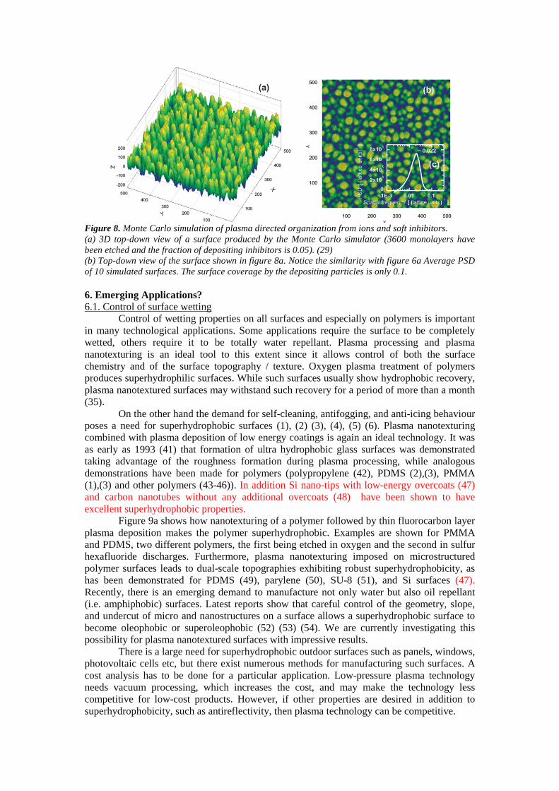
Figure 8. Monte Carlo simulation of plasma directed organization from ions and soft inhibitors.(a) 3D top-down view of a surface produced by the Monte Carlo simulator (3600 monolayers havebeen etched and the fraction of depositing inhibitors is 0.05). (29)(b) Top-down view of the surface shown in figure 8a. Notice the similarity with figure 6a Average PSDof 10 simulated surfaces. The surface coverage by the depositing particles is only 0.1.
6. Emerging Applications? 6.1. Control of surface wetting
Control of wetting properties on all surfaces and especially on polymers is importantin many technological applications. Some applications require the surface to be completelywetted, others require it to be totally water repellant. Plasma processing and plasmananotexturing is an ideal tool to this extent since it allows control of both the surfacechemistry and of the surface topography / texture. Oxygen plasma treatment of polymersproduces superhydrophilic surfaces. While such surfaces usually show hydrophobic recovery,plasma nanotextured surfaces may withstand such recovery for a period of more than a month(35).
On the other hand the demand for self-cleaning, antifogging, and anti-icing behaviourposes a need for superhydrophobic surfaces (1), (2) (3), (4), (5) (6). Plasma nanotexturingcombined with plasma deposition of low energy coatings is again an ideal technology. It wasas early as 1993 (41) that formation of ultra hydrophobic glass surfaces was demonstratedtaking advantage of the roughness formation during plasma processing, while analogousdemonstrations have been made for polymers (polypropylene (42), PDMS (2),(3), PMMA(1),(3) and other polymers (43-46)). In addition Si nano-tips with low-energy overcoats (47)and carbon nanotubes without any additional overcoats (48) have been shown to haveexcellent superhydrophobic properties.
Figure 9a shows how nanotexturing of a polymer followed by thin fluorocarbon layerplasma deposition makes the polymer superhydrophobic. Examples are shown for PMMAand PDMS, two different polymers, the first being etched in oxygen and the second in sulfurhexafluoride discharges. Furthermore, plasma nanotexturing imposed on microstructuredpolymer surfaces leads to dual-scale topographies exhibiting robust superhydrophobicity, ashas been demonstrated for PDMS (49), parylene (50), SU-8 (51), and Si surfaces (47).Recently, there is an emerging demand to manufacture not only water but also oil repellant(i.e. amphiphobic) surfaces. Latest reports show that careful control of the geometry, slope,and undercut of micro and nanostructures on a surface allows a superhydrophobic surface tobecome oleophobic or superoleophobic (52) (53) (54). We are currently investigating thispossibility for plasma nanotextured surfaces with impressive results.
There is a large need for superhydrophobic outdoor surfaces such as panels, windows,photovoltaic cells etc, but there exist numerous methods for manufacturing such surfaces. Acost analysis has to be done for a particular application. Low-pressure plasma technologyneeds vacuum processing, which increases the cost, and may make the technology lesscompetitive for low-cost products. However, if other properties are desired in addition tosuperhydrophobicity, such as antireflectivity, then plasma technology can be competitive.

6.2. Control of optical properties of surfacesReduction of surface reflectivity, with simultaneous preservation of the optical
transparency is often a requirement for many surfaces, such as windows and photovoltaiccells. In other cases roughening is required so as to reduce both reflectivity and transparency.Plasmas are ideal for both applications. Several reports have appeared on this subject andpatents also exist (43, 55) (8). However, the key here is how to control the nanotexture inorder to reduce reflectance for specific wavelength range. Figure 9b shows that reflectivity isindeed reduced significantly by plasma nanotexturing an organic polymer (9). . For short etchtimes the surface remains transparent, while for longer etch times it becomes milky. As analternative to plasma nanotexturing, either plasma organization followed by plasma etching,or some other self-organization technique combined with plasma etching may allow fullcontrol. Indeed, nanosphere lithography followed by plasma etching has been recentlyproposed for antireflective and superhydrophobic surface fabrication (56).
Figure 9. (a) CA and CA hysteresis versus etching time for PDMS and PMMA. The evolution of super-hydrophobicity and the process window for optical transparency are also indicated.(b) Reflection spectra (at 6o) of 2mm PMMA substrates before and after 1, 2, 3 min O2 plasmaprocessing on ONE side of the polymer plate only)(9).
6.3. Polymeric and Silicon Microfluidic Fabrication and modificationWhile for open surfaces plasma technology is in competition with other more “chemical”technologies, it is very appropriate for MEMS fabrication (57-59) and surface modification.For polymeric microfluidics plasma technology is of course in competition with injectionmolding and hot embossing. Nevertheless, the implementation of plasma treatment ofmicrofluidics presents some unique merits in that:
(i) plasma etching is an inherently mass production technique,(ii) the polymer is treated while being in its solid state,(iii) channel formation is performed close to room temperature (cold-plasma),(iv) within the same plasma reactor several surface physicochemical and
mechanical properties (wetability, hardness etc) may be modified,towards the requirements of the specific application,
(v) master fabrication is not needed, hence using only one lithography stepdevices of different depths may be manufactured.
(vi) The high surface area of nanotextured polymers may be used forchromatographic separations, or as reaction sites in a lab-on-a-chip.(58,59)
(vii) Oxygen nanotextured polymeric microfluidics are stable-in-timehydrophilic microchannels, which show capillary pumping. Fluorocarbondeposition through a stencil mask on such microchannels may create
hydrophobic valve areas. Thus, pumping and valving through suchmicrofluidic networks is possible due to plasma technology.
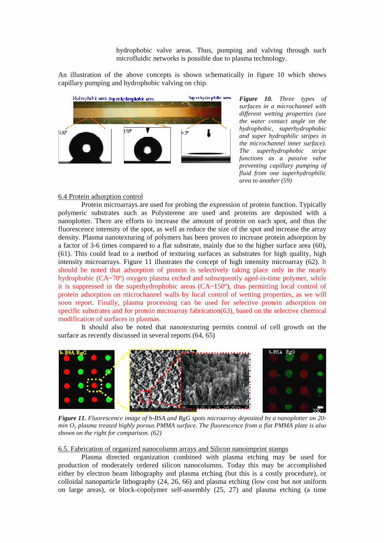
An illustration of the above concepts is shown schematically in figure 10 which showscapillary pumping and hydrophobic valving on chip.
Figure 10. Three types ofsurfaces in a microchannel withdifferent wetting properties (seethe water contact angle on thehydrophobic, superhydrophobicand super hydrophilic stripes inthe microchannel inner surface).The superhydrophobic stripefunctions as a passive valvepreventing capillary pumping offluid from one superhydrophilicarea to another (59)
6.4 Protein adsorption controlProtein microarrays are used for probing the expression of protein function. Typically
polymeric substrates such as Polysterene are used and proteins are deposited with ananoplotter. There are efforts to increase the amount of protein on each spot, and thus thefluorescence intensity of the spot, as well as reduce the size of the spot and increase the arraydensity. Plasma nanotexturing of polymers has been proven to increase protein adsorption bya factor of 3-6 times compared to a flat substrate, mainly due to the higher surface area (60),(61). This could lead to a method of texturing surfaces as substrates for high quality, highintensity microarrays. Figure 11 illustrates the concept of high intensity microarray (62). Itshould be noted that adsorption of protein is selectively taking place only in the nearlyhydrophobic (CA~70º) oxygen plasma etched and subsequently aged-in-time polymer, whileit is suppressed in the superhydrophobic areas (CA~150º), thus permitting local control ofprotein adsorption on microchannel walls by local control of wetting properties, as we willsoon report. Finally, plasma processing can be used for selective protein adsorption onspecific substrates and for protein microarray fabrication(63), based on the selective chemicalmodification of surfaces in plasmas.
It should also be noted that nanotexturing permits control of cell growth on thesurface as recently discussed in several reports (64, 65)
Figure 11. Fluorescence image of b-BSA and RgG spots microarray deposited by a nanoplotter on 20-min O2 plasma treated highly porous PMMA surface. The fluorescence from a flat PMMA plate is alsoshown on the right for comparison. (62)
6.5. Fabrication of organized nanocolumn arrays and Silicon nanoimprint stampsPlasma directed organization combined with plasma etching may be used for
production of moderately ordered silicon nanocolumns. Today this may be accomplishedeither by electron beam lithography and plasma etching (but this is a costly procedure), orcolloidal nanoparticle lithography (24, 26, 66) and plasma etching (low cost but not uniformon large areas), or block-copolymer self-assembly (25, 27) and plasma etching (a time

consuming process) . Thus, plasma directed assembly especially if combined with orderenhancement techniques (graphoepitaxy) may become a promising alternative. Siliconnanopillar arrays may be used as nanoiprint masks for organic polymers or organicphotovoltaics to permit nanostructuring of such materials and thus enhanced efficiency (67) .Work in this direction is already in progress in our team.
7. OutlookPerhaps the biggest problem of plasma technology is the variability from one reactor
system to another and the need to recalibrate processes, when one changes etching system.Plasma nanotexturing / nanoassembly and plasma directed organization being plasma – wallinteraction phenomena add to this variability and may provoke skepticism as to the future ofthis technology. The answer to this challenge will be the design of systems with controlledand adjustable sputtering / deposition. This may be accomplished by a) eliminating sputteringfrom walls and introducing additional sputtering targets in the system, b) allowing control ofwall sputtering, c) eliminating wall sputtering and allowing for gas-phase deposition duringetching. Such solutions demand design of new plasma reactors with embedded or controlledsputtering / deposition sources in close collaboration with equipment manufacturers. Theunderstanding of plasma-surface interactions necessitates also modeling and simulation toolsto aid the design of better plasma systems and processes.
AcknowledgmentsFinancial support through various European and National projects is acknowledged, such asNanoplasma, PENED 03ED202, MD3, Nanotolife, and others. Dr Arun Kumar is kindlyacknowledged for the experiments and SEM images for PMMA films, and Mr AthanasiosSmyrnakis for providing sketches of the plasma reactor. Dr Nikos Vourdas, who was the firstin the group to discover and study plasma directed organization is kindly acknowledged forhis early work. Oxford Instruments Plasma Technology and especially Andy Goodyear andMike Cooke are kindly acknowledged for the experiments done in OIPT in their new plasmasource during the course of the Nanoplasma EU project. Adixen-Alcatel is kindlyacknowledged for kind discussions and support for the equipment operation. AFM imageswere processed using the Software WSxM(36)
1. Vourdas N, Tserepi A, Gogolides E. Nanotextured super-hydrophobic transparentpoly(methyl methacrylate) surfaces using high-density plasma processing. Nanotechnology.2007 Mar 28;18(12):125304.2. Tserepi AD, Vlachopoulou ME, Gogolides E. Nanotexturing ofpoly(dimethylsiloxane) in plasmas for creating robust super-hydrophobic surfaces.Nanotechnology. 2006 Aug 14;17(15):3977-83.3. Tserepi A, Gogolides E, Misiakos K, Vlachopoulou M-E, Vourdas N, inventors;Method for the fabrication of high surface area ratio and high aspect ratio surfaces onsubstrates International Application No PCT/GR2006/000011 Priority Number GR20050100473. 2005.4. Roach P, Shirtcliffe NJ, Newton MI. Progess in superhydrophobic surfacedevelopment. Soft Matter. 2008;4(2):224.5. Crick CR, Parkin IP. Preparation and Characterisation of Super-HydrophobicSurfaces. Chemistry - A European Journal. 2010;16(12):3568-88.6. Bhushan B, Jung YC. Natural and biomimetic artificial surfaces forsuperhydrophobicity, self-cleaning, low adhesion, and drag reduction. Progress in MaterialsScience. 2011;56(1):1-108.7. Jansen HV, de Boer MJ, Unnikrishnan S, Louwerse MC, Elwenspoek MC. Blacksilicon method: X. A review on high speed and selective plasma etching of silicon withprofile control: an in-depth comparison between Bosch and cryostat DRIE processes as aroadmap to next generation equipment. J Micromech Microeng. 2009;19(3):033001.

8. Kaless A, Schulz U, Munzert P, Kaiser N. NANO-motheye antireflection pattern byplasma treatment of polymers. Surface and Coatings Technology. 2005;200(1-4):58-61.9. Gogolides E, Vlachopoulou M, Tsougeni K, Vourdas N, Tserepi A. Micro and nanostructuring and texturing of polymers using plasma processes: Potential manufacturingapplications. International Journal of Nanomanufacturing. 2010;6(1-4):152-63.10. Gogolides E, Constantoudis V, Patsis GP, Tserepi A. A review of line edge roughnessand surface nanotexture resulting from patterning processes. Microelectron Eng. 2006 Apr-Sep;83(4-9):1067-72.11. Seeger K, Palmer RE. Fabrication of silicon cones and pillars using rough metal filmsas plasma etching masks. Appl Phys Lett. 1999;74(11):1627-9.12. Levchenko I, Huang SY, Ostrikov K, Xu S. Silicon on silicon: self-organized nanotiparrays formed in reactive Ar+H2plasmas. Nanotechnology. 2010;21(2):025605.13. Xu S, Levchenko I, Huang SY, Ostrikov K. Self-organized vertically aligned single-crystal silicon nanostructures with controlled shape and aspect ratio by reactive plasmaetching. Appl Phys Lett. 2009;95(11):111505.14. Tam E, Levchenko I, Ostrikov K. Deterministic shape control in plasma-aidednanotip assembly. J Appl Phys. 2006 Aug 1;100(3):036104.15. Levchenko I, Ostrikov K. Nanostructures of various dimensionalities from plasmaand neutral fluxes. J Phys D: Appl Phys. 2007 Apr 21;40(8):2308-19.16. Hsu CH, Lo HC, Chen CF, Wu CT, Hwang JS, Das D, et al. Generally applicableself-masked dry etching technique for nanotip array fabrication. Nano Letters. 2004;4(3):471-5.17. Park CK, Kim HT, Kim DY, Lee NE. Formation of silicon nitride nanopillars in dual-frequency capacitively coupled plasma and their application to Si nanopillar etching. J VacSci Technol A. 2007;25(4):1073-7.18. Gharghi M, Sivoththaman S. Formation of nanoscale columnar structures in siliconby a maskless reactive ion etching process. J Vac Sci Technol A. 2006;24(3):723-7.19. Zheng J, Yang R, Xie L, Qu J, Liu Y, Li X. Plasma-Assisted Approaches in InorganicNanostructure Fabrication. Advanced Materials. 2010;22(13):1451-73.20. Levchenko I, Ostrikov K, Diwan K, Winkler K, Mariotti D. Plasma-driven self-organization of Ni nanodot arrays on Si(100). Appl Phys Lett. 2008;93(18):183102.21. Ostrikov K. Plasma nanoscience: From nature's mastery to deterministic plasma-aided nanofabrication. Ieee T Plasma Sci. 2007 Apr;35(2):127-36.22. Bowden N, Brittain S, Evans AG, Hutchinson JW, Whitesides GM. Spontaneousformation of ordered structures in thin films of metals supported on an elastomeric polymer.Nature. 1998 May 14;393(6681):146-9.23. Tsougeni K, Boulousis G, Gogolides E, Tserepi A. Oriented spontaneously formednano-structures on poly(dimethylsiloxane) films and stamps treated in O-2 plasmas.Microelectron Eng. 2008 May-Jun;85(5-6):1233-6.24. Boal AK, Ilhan F, Derouchey JE, Thurn-Albrecht T, Russell TP, Rotello VM. Self-assembly of nanoparticles into structured spherical and network aggregates. Nature.2000;404(6779):746-8.25. Park C, Yoon J, Thomas EL. Enabling nanotechnology with self assembled blockcopolymer patterns. Polymer. 2003;44(22):6725-60.26. Hulteen JC, Van Duyne RP. Nanosphere lithography: A materials general fabricationprocess for periodic particle array surfaces. J Vac Sci Technol A. 1995;13(3):1553-8.27. Ting YH, Park SM, Liu CC, Liu XS, Himpsel FJ, Nealey PF, et al. Plasma etchremoval of poly(methyl methacrylate) in block copolymer lithography. J Vac Sci Technol B.2008 Sep-Oct;26(5):1684-9.28. Gogolides E, Tserepi A, Constantoudis V, Vourdas N, Boulousis G, VlachopoulouME, et al., inventors; Method for the fabrication of periodic structures on polymers usingplasma processes International Application No PCT/GR2009/000039 Priority Number GR20080100404. 2008.

29. Vourdas N, Kontziampasis D, Kokkoris G, Constantoudis V, Goodyear A, Tserepi A,et al. Plasma directed assembly and organization: bottom-up nanopatterning using top-downtechnology. Nanotechnology. 2010 Feb 26;21(8):085302.30. Frost F, Ziberi B, Hoche T, Rauschenbach B. The shape and ordering of self-organized nanostructures by ion sputtering. Nucl Instrum Methods B. 2004 10 June 2003through 13 June 2003;216(1-4):9-19.31. Frost F, Ziberi B, Schindler A, Rauschenbach B. Surface engineering with ion beams:From self-organized nanostructures to ultra-smooth surfaces. Appl Phys A. 2008;91(4):551-9.32. Gago R. Self-organized surface nanopatterning by ion beam sputtering in TowardFunctional Nanomaterials. In: Wang ZM, editor. Lecture Notes in Nanoscale Science andTechnology: Springer; 2009.33. Kokkoris G, Constantoudis V, Angelikopoulos P, Boulousis G, Gogolides E. Dualnanoscale roughness on plasma-etched Si surfaces: Role of etch inhibitors. Phys Rev B.2007;76(19):193405.34. Engelmann S, Bruce RL, Weilnboeck F, Oehrlein GS, Nest D, Graves DB, et al.Dependence of Polymer Surface Roughening Rate on Deposited Energy Density DuringPlasma Processing. Plasma Process Polym. 2009;6(8):484-9.35. Tsougeni K, Vourdas N, Tserepi A, Gogolides E, Cardinaud C. Mechanisms ofOxygen Plasma Nanotexturing of Organic Polymer Surfaces: From Stable Super Hydrophilicto Super Hydrophobic Surfaces. Langmuir. 2009 Oct 6;25(19):11748-59.36. Horcas I, Fernandez R, Gomez-Rodriguez JM, Colchero J, Gomez-Herrero J, BaroAM. WSXM: A software for scanning probe microscopy and a tool for nanotechnology.Review of Scientific Instruments. 2007 Jan;78(1):-. 37. Martin M, Cunge G. Surface roughness generated by plasma etching processes ofsilicon. Journal of Vacuum Science & Technology B: Microelectronics and NanometerStructures. 2008;26(4):1281.38. Boulousis G, Constantoudis V, Kokkoris G, Gogolides E. Formation and metrologyof dual scale nano-morphology on SF6 plasma etched silicon surfaces. Nanotechnology. 2008Jun 25;19(25):-. 39. Ramos R, Cunge G, Joubert O, Sadeghi N, Mori M, Vallier L. Plasma/reactor wallsinteractions in advanced gate etching processes. Thin Solid Films. 2007;515(12):4846-52.40. Pelliccione M, Karabacak T, Gaire C, Wang GC, Lu TM. Mound formation insurface growth under shadowing. Phys Rev B. 2006;74(12):125420.41. Ogawa K, Soga M, Takada Y, Nakayama I. Development of a transparent andultrahydrophobic glass plate. Japanese Journal of Applied Physics, Part 2: Letters. 1993;32(4B).42. Youngblood JP, McCarthy TJ. Ultrahydrophobic polymer surfaces prepared bysimultaneous ablation of polypropylene and sputtering of poly(tetrafluoroethylene) usingradio frequency plasma. Macromolecules. 1999 Oct 5;32(20):6800-6.43. Di Mundo R, De Benedictis V, Palumbo F, d’Agostino R. Fluorocarbon plasmas fornanotexturing of polymers: A route to water-repellent antireflective surfaces. Applied SurfaceScience. 2009;255(10):5461-5.44. Milella A, Di Mundo R, Palumbo F, Favia P, Fracassi F, d'Agostino R. PlasmaNanostructuring of Polymers: Different Routes to Superhydrophoblicity. Plasma ProcessPolym. 2009 Jul 18;6(6-7):460-6.45. Di Mundo R, Palumbo F, d'Agostino R. Nanotexturing of polystyrene surface influorocarbon plasmas: From sticky to slippery superhydrophobicity. Langmuir. 2008 May6;24(9):5044-51.46. Favia P, Cicala G, Milella A, Palumbo F, Rossini R, d'Agostino R. Deposition ofsuper-hydrophobic fluorocarbon coatings in modulated RF glow discharges. Surf Coat Tech.2003 Jun 2;169:609-12.47. Shieh J, Hou FJ, Chen YC, Chen HM, Yang SP, Cheng CC, et al. Robust AirlikeSuperhydrophobic Surfaces. Advanced Materials. 2010 Feb 2;22(5):597-+.
48. Han Z, Tay B, Tan C, Shakerzadeh M, Ostrikov K. Electrowetting control of Cassie-to-Wenzel transitions in superhydrophobic carbon nanotube-based nanocomposites. ACSNano. 2009;3(10):3031-6.49. Cortese B, D'Amone S, Manca M, Viola I, Cingolani R, Gigli G.Superhydrophobicity due to the hierarchical scale roughness of PDMS surfaces. Langmuir.2008 Mar 18;24(6):2712-8.50. Chen MH, Hsu TH, Chuang YJ, Tseng FG. Dual hierarchical biomimicsuperhydrophobic surface with three energy states. Appl Phys Lett. 2009 Jul 13;95(2):-. 51. Marquez-Velasco J, Vlachopoulou ME, Tserepi A, Gogolides E. Stablesuperhydrophobic surfaces induced by dual-scale topography on SU-8. Microelectron Eng.2010 May-Aug;87(5-8):782-5.52. Wang C-F, Chiou S-F, Ko F-H, Chou C-T, Lin H-C, Huang C-F, et al. Fabrication ofBiomimetic Super-Amphiphobic Surfaces Through Plasma Modification of BenzoxazineFilms. Macromolecular Rapid Communications. 2006;27(5):333-7.53. Tuteja A, Choi W, Ma M, Mabry JM, Mazzella SA, Rutledge GC, et al. DesigningSuperoleophobic Surfaces. Science. 2007;318(5856):1618-22.54. Liu M, Wang S, Wei Z, Song Y, Jiang L. Bioinspired Design of a Superoleophobicand Low Adhesive Water/Solid Interface. Advanced Materials. 2009;21(6):665-9.55. Wang Y, Lu N, Xu H, Shi G, Xu M, Lin X, et al. Biomimetic corrugated siliconnanocone arrays for self-cleaning antireflection coatings. Nano Research. 2010;3(7):520-7.56. Li Y, Zhang J, Zhu S, Dong H, Jia F, Wang Z, et al. Bioinspired Silica Surfaces withNear-Infrared Improved Transmittance and Superhydrophobicity by Colloidal Lithography.Langmuir. 2010;26(12):9842-7.57. Rossier JlS, Vollet C, Carnal A, Lagger Gg, Gobry Vr, Girault HH, et al. Plasmaetched polymer microelectrochemical systems. Lab Chip. 2002;2(3):145.58. Nabesawa H, Hitobo T, Wakabayashi S, Asaji T, Abe T, Seki M. Polymer surfacemorphology control by reactive ion etching for microfluidic devices. Sensors and ActuatorsB: Chemical. 2008;132(2):637-43.59. Tsougeni K, Papageorgiou D, Tserepi A, Gogolides E. "Smart'" polymericmicrofluidics fabricated by plasma processing: controlled wetting, capillary filling andhydrophobic valving. Lab Chip. 2010;10(4):462-9.60. Vlachopoulou ME, Petrou PS, Kakabakos SE, Tserepi A, Gogolides E. High-aspect-ratio plasma-induced nanotextured poly(dimethylsiloxane) surfaces with enhanced proteinadsorption capacity. J Vac Sci Technol B. 2008 Nov;26(6):2543-8.61. Tsougeni K, Petrou PS, Tserepi A, Kakabakos SE, Gogolides E. Nano-texturing ofpoly(methyl methacrylate) polymer using plasma processes and applications in wettingcontrol and protein adsorption. Microelectron Eng. 2009 Apr-Jun;86(4-6):1424-7.62. Tsougeni K, Tserepi A, Constantoudis V, Gogolides E, Petrou PS, Kakabakos SE.Plasma Nanotextured PMMA Surfaces for Protein Arrays: Increased Protein Binding andEnhanced Detection Sensitivity. Langmuir. 2010 Sep 7;26(17):13883-91.63. Bayiati P, Malainou A, Matrozos E, Tserepi A, Petrou PS, Kakabakos SE, et al. High-density protein patterning through selective plasma-induced fluorocarbon deposition on Sisubstrates. Biosensors and Bioelectronics. 2009;24(10):2979-84.64. Gristina R, D'Aloia E, Senesi GS, Milella A, Nardulli M, Sardella E, et al. Increasingcell adhesion on plasma deposited fluorocarbon coatings by changing the surface topography.Journal of Biomedical Materials Research Part B: Applied Biomaterials. 2009;88B(1):139-49.65. Sardella E, Detomaso L, Gristina R, Senesi GS, Agheli H, Sutherland DS, et al.Nano-Structured Cell-Adhesive and Cell-Repulsive Plasma-Deposited Coatings: Chemicaland Topographical Effects on Keratinocyte Adhesion. Plasma Process Polym. 2008;5(6):540-51.66. Zhang J, Li Y, Zhang X, Yang B. Colloidal Self-Assembly Meets Nanofabrication:From Two-Dimensional Colloidal Crystals to Nanostructure Arrays. Advanced Materials.2010;22(38):4249-69.

67. Cheyns D, Vasseur K, Rolin C, Genoe J, Poortmans J, Heremans P. Nanoimprintedsemiconducting polymer films with 50 nm features and their application to organicheterojunction solar cells. Nanotechnology. 2008 Oct 22;19(42):-.
∗ corresponding author e-mail: [email protected]