Embed Size (px)
Citation preview
Nanoscale
PAPER
Cite this: Nanoscale, 2020, 12, 21757
Received 29th July 2020,Accepted 6th October 2020
DOI: 10.1039/d0nr05630h
rsc.li/nanoscale
Controlling palladium morphology inelectrodeposition from nanoparticles todendrites via the use of mixed solvents†
Haytham E. M. Hussein, a,b Houari Amari, c,d Ben G. Breeze, c
Richard Beanland c and Julie V. Macpherson *a
By changing the mole fraction of water (χwater) in the solvent acetonitrile (MeCN), we report a simple pro-
cedure to control nanostructure morphology during electrodeposition. We focus on the electrodeposi-
tion of palladium (Pd) on electron beam transparent boron-doped diamond (BDD) electrodes. Three solu-
tions are employed, MeCN rich (90% v/v MeCN, χwater = 0.246), equal volumes (50% v/v MeCN, χwater =
0.743) and water rich (10% v/v MeCN, χwater = 0.963), with electrodeposition carried out under a constant,
and high overpotential (−1.0 V), for fixed time periods (50, 150 and 300 s). Scanning transmission electron
microscopy (STEM) reveals that in MeCN rich solution, Pd atoms, amorphous atom clusters and (majority)
nanoparticles (NPs) result. As water content is increased, NPs are again evident but also elongated and
defected nanostructures which grow in prominence with time. In the water rich environment, NPs and
branched, concave and star-like Pd nanostructures are now seen, which with time translate to aggregated
porous structures and ultimately dendrites. We attribute these observations to the role MeCN adsorption
on Pd surfaces plays in retarding metal nucleation and growth.
Introduction
In electrochemical devices used for energy conversion, nano-structures such as nanoparticles (NPs), made of metals, forexample the platinum group metals, control the electrocataly-sis process.1–3 The electrocatalytic reaction can be optimisedby careful control of the metal catalyst crystal structure, size,loading, presence of defects etc.4–9 The need to produceeffective electrocatalysts has led to the exploration of manydifferent chemical and physical NP and nanostructure syn-thesis strategies.2,10,11 These include chemical vapour depo-sition, atomic layer deposition, colloidal synthesis, sputteringetc.12–16 Palladium (Pd) is an interesting metal due to its use in
the production of hydrogen from the electrochemical watersplitting reaction and hydrogen storage.1,17 To move from lab-oratory based research to commercial applications, low cost,scalable methods of nanostructure fabrication are essential.17
Electrodeposition offers an interesting route for nano-material production, as it is effectively bottom-up synthesis,lends itself to scalability, and does not require sophisticatedinstruments or a high technical level of training.18–22
Electrodeposition also offers a wide variety of tuneable para-meters for controlling nanostructure morphology, theseinclude e.g. electrode deposition potential and time of depo-sition, temperature, and electrolyte composition.23–26 It is thusnot surprising that electrodeposition has been used to make avariety of controlled Pd nanostructures such as nanowires,17
cubes, nanoflowers, nanoframes, and high index faceted Pdnanocrystals.11,27–29
Interestingly, despite the vast number of electrodepositionstudies, the majority are carried out in aqueous solutions, as isthe case for Pd, using salts that contain anions such as Cl−,ClO4
−, SO4−2, NO3
−.30 Few studies use different salt andsolvent systems, and even less consider the role mixed solventsystems can play in controlling deposition morphology.31
Changing solvent can offer advantages to electrodepositionsuch as changing the (i) double layer structure, which includesthe impact of solvent adsorption, (ii) solvation shell structure,(iii) redox potential, (iv) metal reduction electron transfer
†Electronic supplementary information (ESI) available: Assignment of theRaman spectra recorded in the three different MeCN–water solutions. ESI2:Cyclic voltammetry of Pd-acetate in the three different MeCN–water solutions.ESI3: High resolution ADF-STEM of Pd nanostructure electrodeposition. ESI4:Statistical analysis for Pd nanostructures electrodeposited for tdep = 50 s and 15s. (PDF). See DOI: 10.1039/d0nr05630h
aDepartment of Chemistry, University of Warwick, Coventry, CV4 7AL, UK.
E-mail: [email protected]; Fax: +44 (0) 2476 524112;
Tel: +44 (0) 2476 573886bDepartment of Chemistry, University of Southampton, SO17 1BJ, UKcDepartment of Physics, University of Warwick, Coventry, CV4 7AL, UKdLeibniz-Institut fuer Kristallzuechtung (IKZ), Max-Born-Str. 2, 12489 Berlin,
Germany
This journal is © The Royal Society of Chemistry 2020 Nanoscale, 2020, 12, 21757–21769 | 21757
Ope
n A
cces
s A
rtic
le. P
ublis
hed
on 1
5 O
ctob
er 2
020.
Dow
nloa
ded
on 2
/8/2
022
10:3
7:21
AM
. T
his
artic
le is
lice
nsed
und
er a
Cre
ativ
e C
omm
ons
Attr
ibut
ion
3.0
Unp
orte
d L
icen
ce.
View Article OnlineView Journal | View Issue
kinetics, (v) altering the diffusional properties of ions in thesolvent, (vi) increasing the potential window, enabling metalreduction outside the aqueous solvent window, and (vii)increasing the variety of electrodeposition salts which can bedissolved etc.32
Mixing two or more (miscible) solvents together offersa further control parameter in the study of electro-deposition.23,31,33 Whilst each solvent possesses its ownchemical and physical characteristics,33 when mixed the struc-ture and physical properties of each individual solvent com-ponent, the solvation state of the metal ion, the electricaldouble layer, along with the other factors highlighted above,will change depending on the mole fraction of the individualsolvent in the solution.33 For example, in batteries it hasalready been shown that by moving to mixed-solvents, metaldendrite formation can be suppressed34 and in electrocataly-sis, water molecule reactivity can be increased through water-solvent co-ordination bonding.35 Furthermore, many of thestudies that work in a non-aqueous solvent system, be itorganic, ionic liquid or deep eutectic solvents are in realityhighly likely to be mixed solvent due to the uptake of tracewater, which can be difficult to exclude completely.36
In this work we investigate the electrodeposition of Pd,from its metallo-organic salt (Pd-acetate) in miscible organic–aqueous solvents; here water and acetonitrile (MeCN), underorganic rich (90% : 10% MeCN : water v/v), water rich(10% : 90% MeCN : water v/v) and equal contributions of bothsolvent by volume (50% : 50% v/v), conditions. We provideinsights into how MeCN and water bulk solvent structures aremodified by the presence of the second solvent and explorethe role the water–MeCN mixed solvent systems play in control-ling atom level and nanoscale electrodeposition of Pd.
ExperimentalChemicals and solution preparation
Experiments were carried out using mixed-solvent systems,prepared using variable ratios of MeCN, water, tetrabutylammonium tetrafluoroborate (Bu4N·BF4), and KCl, whilekeeping the concentration of Pd-acetate fixed at 1 × 10⁻³ M.Solution 1 (organic rich) is made of 1 × 10⁻³ M Pd-acetate +0.1 M Bu4N·BF4 in 90% : 10% MeCN : water v/v; correspondsto a mole fraction (χ) of χMeCN = 0.757 + χwater = 0.243.Solution 2 is made of 1 × 10⁻³ M Pd-acetate + 0.05 MBu4N·BF4 + 0.05 M KCl in 50% : 50% MeCN : water v/v (χMeCN =0.257 + χwater = 0.743). Solution 3 (water rich) is made of1 × 10−3 M Pd-acetate + 0.08 M KCl in 10% : 90% MeCN : waterv/v (χMeCN = 0.037 + χwater = 0.963 (10% : 90% v/v). The solu-tions were prepared with trace element grade chemicals, andall chemicals were used as received without further purifi-cation. 99.99% HPLC far UV-Vis grade MeCN and deionisedwater from a Purite Select HP system were used for solutionpreparation (with a resistivity of 18.2 MΩ cm at 25 °C). Pure99.999% Ar and N2 (BOC industries, UK) were used to de-aerate the solutions.
Electrochemical studies
Electrochemical measurements were performed using a CHIpotentiostat (750C) and IVIUM Compactstat potentiostat in athree-electrode configuration with a Ag|Ag+ double junctionreference electrode. The reference electrode was constructedfrom Ag wire immersed in a MeCN solution containing 0.1 MBu4N·BF4 and separated from a compartment containing thesame solution by a porous Vycor tip (BASI). The working elec-trodes were produced from a freestanding microcrystallineBDD wafer (boron dopant level of ∼3 × 10²⁰ B atoms per cm3)grown using microwave chemical vapor deposition (ElementSix, Harwell, Oxford, UK). For all electrochemical experiments,BDD transmission electron microscopy (TEM) supports, with a(110) crystalline surface texture, which also function as electro-des, were employed.37 These were made from the BDD waferthinned down to ∼50 μm thickness by mechanical polishing,with both sides showing a surface roughness of ca. 0.17 nm(measured using atomic force microscopy) on the surface of agrain (grain size ca. 2–8 μm). The thinned wafers were thencut into 3 mm diameter disks using laser micromachining(355 nm Nd:YAG laser micromachiner, E-355-ATHI-O system,Oxford Lasers Ltd UK, with a nominal pulse-length of 34 ns).The supports were acid cleaned in KNO3/H2SO4 solution toremove debris after laser micro-machining. To produce areasof electron transparency the supports were Ar+ ion milled at anaccelerating voltage of 6 kV and an angle of incidence of ∼4°;the preparation procedure is described in detail in ref. 37.After ion milling, the BDD was acid cleaned using 0.1 M HNO3
followed by 0.1 M H2SO4 and then washed carefully in deio-nised water. To make an ohmic contact to the TEM electrode,the upper quarter of one of the edges was sputtered (MoorfieldMiniLab 060 Platform) with Ti (20 nm)/Au (400 nm) andannealed in a tube furnace for 5 h at 450 °C. The electro-chemical set-up showing how to use the BDD TEM support/electrode is described in ref. 37. Electrodeposition takes placeon both sides of the support over an area of ∼0.06 cm2.
Microscopy characterisation
Microscopic studies were carried out ex situ after electrodeposi-tion on the TEM BDD electrode. Before imaging, the electrodewas gently rinsed with de-oxygenated water, dried under inertatmosphere and kept in a desiccator to avoid any contami-nation during transfer. The morphology of the deposited Pdmaterial on the TEM electrodes were characterised by ex situtechniques using field emission scanning electron microscopy(FE-SEM) for low magnification and annular dark-field scan-ning transmission electron microscopy (ADF-STEM) for higherresolution. FE-SEM images were recorded using the in-lens,EsB, SE2 and STEM detectors on a Zeiss Gemini or Zeiss Supra55-VP operating at 5 kV, 15 kV and 25 kV, respectively. For eachdeposition, at least three images (n = 3) were recorded indifferent areas of the surface for both FE-SEM and ADF-STEMmeasurements and an average of 150 Pd nanostructures ana-lysed. ADF-STEM images were obtained using a double aberra-tion corrected JEOL JEM-ARM200F at 200 kV using an annularfield detector with a fine-imaging probe of FWHM ∼0.085 nm,
Paper Nanoscale
21758 | Nanoscale, 2020, 12, 21757–21769 This journal is © The Royal Society of Chemistry 2020
Ope
n A
cces
s A
rtic
le. P
ublis
hed
on 1
5 O
ctob
er 2
020.
Dow
nloa
ded
on 2
/8/2
022
10:3
7:21
AM
. T
his
artic
le is
lice
nsed
und
er a
Cre
ativ
e C
omm
ons
Attr
ibut
ion
3.0
Unp
orte
d L
icen
ce.
View Article Online
and probe current of 23 pA with a convergence semi-angle of∼25 mrad and an inner angle of 50 mrad.
X-ray energy dispersive spectrometry (XEDS) spectra wererecorded using the XEDS unit (Oxford Instruments) with theFE-SEM, at a working distance of 10 mm and acceleratingvoltage of 15 kV. Raman was conducted on a Horiba LabRamHR Evolution Raman microscope at room temperature, withlaser wavelengths of 660 nm (100 mW), 660 nm edge laserfilter, 1800 mm−1 gratings, laser power 100% (50 mW), and150 μm iris size. LabRam was equipped with a UV-Vis-NIRmacro multipass cuvette cell holder and the samples were in aQuartz Cuvette.
Results and discussionSolvent–solvent interactions in MeCN–water systems
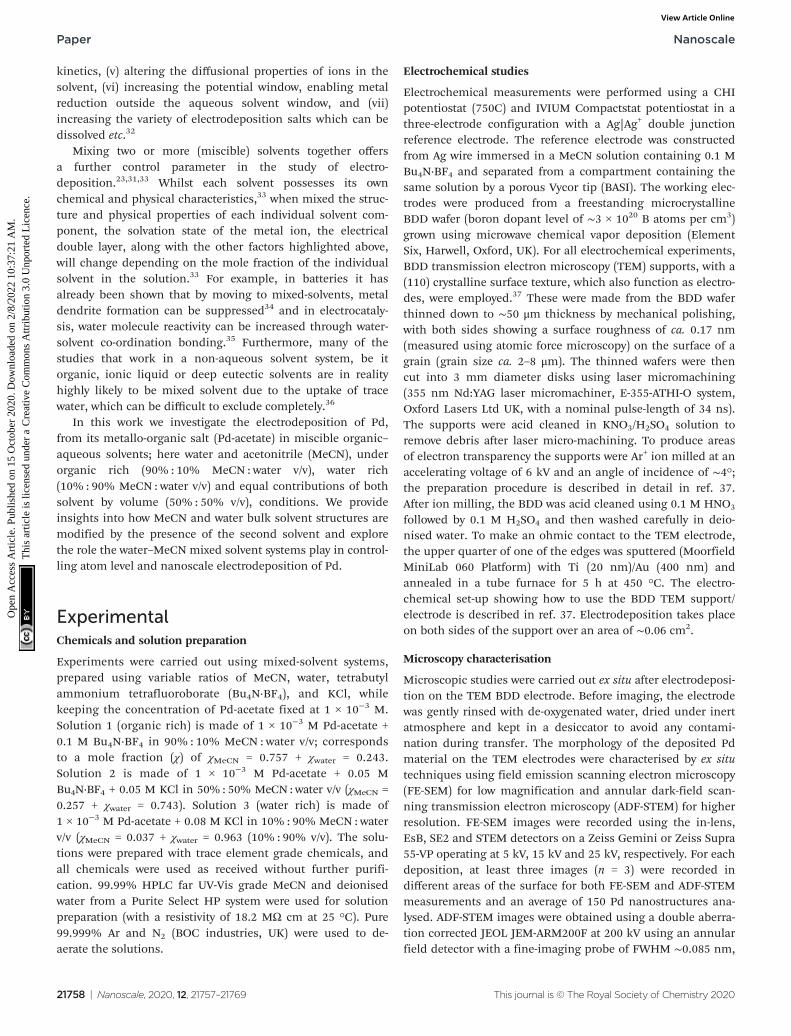
Raman microscopy was used to provide information onchanges in intra- and inter-solvent–solvent interactions as thewater content in MeCN was increased. The Raman spectra ofthe three solutions containing 1 × 10⁻³ M Pd-acetate in (1)organic rich, 90% MeCN : 10% water v/v (χwater = 0.243); (2)equal by volume MeCN and water i.e. 50% MeCN : 50% water
v/v (χwater = 0.743), and (3) water rich, 10% MeCN : 90% waterv/v (χwater = 0.963) solutions, are shown in Fig. 1, and ESI1,Fig. S1.† The vibrational stretching mode band assignmentsfor CuN and C–H (MeCN) and O–H (water) are listed in ESI1,Table S1† and assist with peak labelling in Fig. 1.
Fig. 1(a) shows the Raman spectral region associated withthe CuN stretch of MeCN whilst Fig. 1(b) shows the Ramanspectral region of both the C–H and O–H38–40 stretches, associ-ated with MeCN and water, respectively. The emergence of theO–H band is associated with a tetrahedrally hydrogen-bondednetwork of water molecules i.e. bulk water,38 whilst the C–Hand CuN bands are associated with the MeCN molecules. Thedifferent coloured lines represent the different solutions aswater content is increased (expressed in terms of water molefraction, χwater, in the solution). Grey is χwater = 0.243 (solution1, organic rich), red is χwater = 0.743 (solution 2, equal volume),and green is χwater = 0.963 (solution 3, water rich).
Monitoring changes in the position and intensity of bandsin the different Raman regions as a function of χwater can beused as a diagnostic for how inter- and intra-solvent bondinginteractions change.38–40 Qualitatively, as water contentincreases both the CuN and C–H bands shift to a higher wave-number and the intensity decreases. Only in solution 3 was an
Fig. 1 Raman spectra of (a) CuN (MeCN), and (bi) C–H (MeCN) and O–H (water) stretches as function of increasing water mole fraction χwater, (bii)is a zoom-in to the spectra shown in bi. Grey line represents solution 1 = 90% MeCN : 10% water v/v (χwater = 0.243), red line represents solution 2 =50% MeCN : 50% water v/v (χwater = 0.743) and the green line represents solution 3 = 10% MeCN : 90% water v/v (χwater = 0.963). All contain 1 × 10⁻³
M Pd-acetate.
Nanoscale Paper
This journal is © The Royal Society of Chemistry 2020 Nanoscale, 2020, 12, 21757–21769 | 21759
Ope
n A
cces
s A
rtic
le. P
ublis
hed
on 1
5 O
ctob
er 2
020.
Dow
nloa
ded
on 2
/8/2
022
10:3
7:21
AM
. T
his
artic
le is
lice
nsed
und
er a
Cre
ativ
e C
omm
ons
Attr
ibut
ion
3.0
Unp
orte
d L
icen
ce.
View Article Online
O–H band recorded. This behaviour can be interpreted from amicroheterogeneity viewpoint.38,41,42 In solution 1 (MeCN/organic rich), the absence of an O–H band indicates that theminority water molecules exist as discrete molecules and areunable to form a hydrogen bonded water network. In solution2, as the water content increases, the percentage of MeCNmolecules coordinated to water through H-bond interactionsincreases as evidenced by the positive shift of the CuN Ramanbands. In solution 3 (water rich), there is enough water toform a H-bonded water network and the characteristic O–Hband is observed.
The CuN Raman spectral region in Fig. 1(a), and ESI1,Fig. S2 and S3,† can be fit with two components, one that isassociated with bulk MeCN (recorded at low Raman shift), anda second associated with MeCN bound to water molecules(recorded at higher Raman shift). Using the Shurvell method43
it is possible to determine the fraction of MeCN moleculesbound to MeCN molecules, as water content increases. In solu-tion 1, this fraction is determined as 0.83 i.e. the majority ofMeCN are binding to other MeCN, whilst in solutions 2 and 3this fraction decreases to 0.67 and 0, respectively i.e. in thepresence of 90% water, all the MeCN molecules exist bound towater.
Electrodeposition
To explore the impact of χwater in MeCN on the resulting Pdmorphology, nucleation and growth was monitored as a func-tion of time in the three different MeCN : water mixtures con-taining the Pd-acetate salt. The corresponding CVs for electro-deposition in each solution are shown in ESI2, Fig. S4.† TheCVs show that in the MeCN rich solution, electrodepositioninitiates at a potential Edep vs. Ag|Ag+ ∼ −1.0 V, with amaximum current occurring at −1.26 V vs. Ag|Ag+. As watercontent increases, Edep shifts more positive, up to ∼0.5 V inthe water rich solution, indicating that the process is becom-ing more kinetically favourable in the presence of water. Note,in MeCN only (no water present) it has been previously shownusing IR, NMR, XRD, and UV-vis that electrodeposition of Pdis not possible as the acetate ligands (bound trimerically,Pd3(acetate)6) remain co-ordinated during reduction of Pd2+ toPd(0).44 In the organic rich solution, adding a small amount ofwater (10% v/v, (χwater = 0.243) results in partial destabilisationof the Pd-acetate bond due the strength of the interactionbetween water and acetate overcoming that between Pd andacetate.44 This results in water preferentially binding to theacetate ligands and freeing up the Pd cation for solvation byMeCN, Pd can now electrodeposit.
To investigate how water content affects the morphology ofthe resulting Pd nanostructures at atom level resolution,ADF-STEM images were recorded of the Pd deposits formeddirectly on an electron transparent BDD electrode. Using acombined TEM substrate–electrode allows direct interrog-ation of electrodeposition structures on the electrode withoutthe need for material transfer (and possible loss or modifi-cation of deposited material). The same three solutions wereused, as in Fig. 1 which progressively increase in water
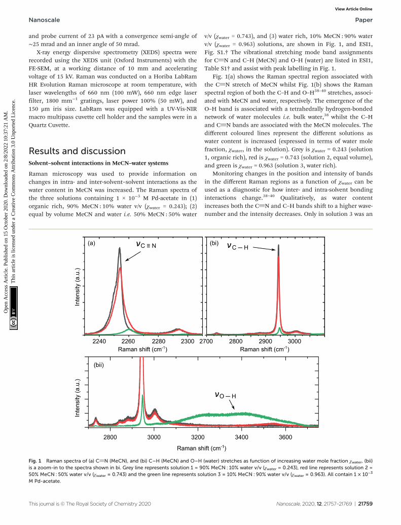
content. An overpotential, η = −1.0 V, with an initial depo-sition time, tdep = 50 s was employed for these studies. Thelarge overpotential means that for all three systems electrode-position is likely to be under mass-transport (diffusion)limited conditions, for a sufficient period of time to formnanostructures. Note electrodeposition occurs on both facesof the BDD TEM electrode, as shown by the nanostructureslabelled by the green (front face) and blue (back face) arrowsin Fig. 2.
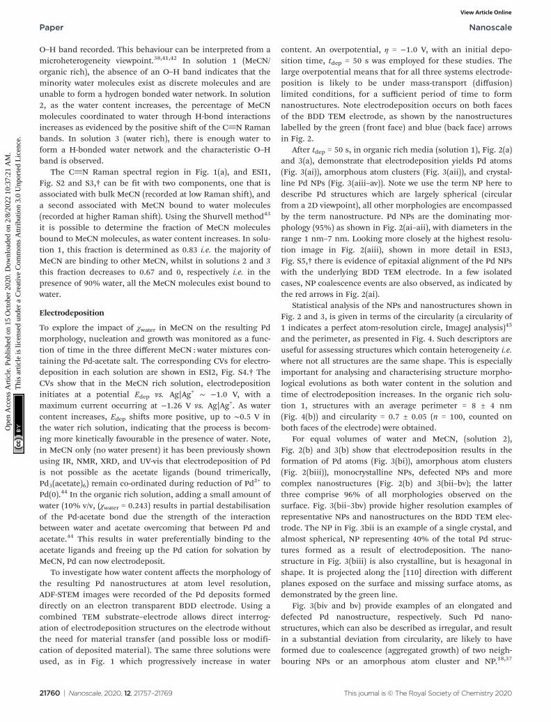
After tdep = 50 s, in organic rich media (solution 1), Fig. 2(a)and 3(a), demonstrate that electrodeposition yields Pd atoms(Fig. 3(ai)), amorphous atom clusters (Fig. 3(aii)), and crystal-line Pd NPs (Fig. 3(aiii–av)). Note we use the term NP here todescribe Pd structures which are largely spherical (circularfrom a 2D viewpoint), all other morphologies are encompassedby the term nanostructure. Pd NPs are the dominating mor-phology (95%) as shown in Fig. 2(ai–aii), with diameters in therange 1 nm–7 nm. Looking more closely at the highest resolu-tion image in Fig. 2(aiii), shown in more detail in ESI3,Fig. S5,† there is evidence of epitaxial alignment of the Pd NPswith the underlying BDD TEM electrode. In a few isolatedcases, NP coalescence events are also observed, as indicated bythe red arrows in Fig. 2(ai).
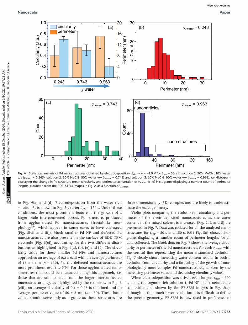
Statistical analysis of the NPs and nanostructures shown inFig. 2 and 3, is given in terms of the circularity (a circularity of1 indicates a perfect atom-resolution circle, ImageJ analysis)45
and the perimeter, as presented in Fig. 4. Such descriptors areuseful for assessing structures which contain heterogeneity i.e.where not all structures are the same shape. This is especiallyimportant for analysing and characterising structure morpho-logical evolutions as both water content in the solution andtime of electrodeposition increases. In the organic rich solu-tion 1, structures with an average perimeter = 8 ± 4 nm(Fig. 4(b)) and circularity = 0.7 ± 0.05 (n = 100, counted onboth faces of the electrode) were obtained.
For equal volumes of water and MeCN, (solution 2),Fig. 2(b) and 3(b) show that electrodeposition results in theformation of Pd atoms (Fig. 3(bi)), amorphous atom clusters(Fig. 2(biii)), monocrystalline NPs, defected NPs and morecomplex nanostructures (Fig. 2(b) and 3(bii–bv); the latterthree comprise 96% of all morphologies observed on thesurface. Fig. 3(bii–3bv) provide higher resolution examples ofrepresentative NPs and nanostructures on the BDD TEM elec-trode. The NP in Fig. 3bii is an example of a single crystal, andalmost spherical, NP representing 40% of the total Pd struc-tures formed as a result of electrodeposition. The nano-structure in Fig. 3(biii) is also crystalline, but is hexagonal inshape. It is projected along the [110] direction with differentplanes exposed on the surface and missing surface atoms, asdemonstrated by the green line.
Fig. 3(biv and bv) provide examples of an elongated anddefected Pd nanostructure, respectively. Such Pd nano-structures, which can also be described as irregular, and resultin a substantial deviation from circularity, are likely to haveformed due to coalescence (aggregated growth) of two neigh-bouring NPs or an amorphous atom cluster and NP.18,37
Paper Nanoscale
21760 | Nanoscale, 2020, 12, 21757–21769 This journal is © The Royal Society of Chemistry 2020
Ope
n A
cces
s A
rtic
le. P
ublis
hed
on 1
5 O
ctob
er 2
020.
Dow
nloa
ded
on 2
/8/2
022
10:3
7:21
AM
. T
his
artic
le is
lice
nsed
und
er a
Cre
ativ
e C
omm
ons
Attr
ibut
ion
3.0
Unp
orte
d L
icen
ce.
View Article Online
Whilst, such events have been seen before in electrodepositionthey are often associated with much shorter timescales (earlystage growth).18,37,46–48 The observation of an increasingnumber of such structures demonstrates how increasing watercontent is influencing the growth process. The average per-imeter of all assessed nanostructures (n = 200) for electrodepo-sition is now 11 ± 6 nm (Fig. 4(c)) with an average circularityvalue of 0.5 ± 0.1 (Fig. 4(a)). The drop of the circularity valueaccompanied with an increase in the perimeter value, high-lights the increased prominence of the more elongated/defected nanostructures as seen in Fig. 2(bi and bii).
Electrodeposition of Pd nanostructures in water rich media(χwater = 0.963, solution 3) is shown in Fig. 2(c) and 3(c). Aftertdep = 50 s, the following nanostructures exist; Pd atoms (Fig. 3(ci)), amorphous atom clusters (Fig. 2(ciii)), both monocrystal-line and defected Pd NPs with diameters in the range 3 nm to7 nm (comprising 70% of all structures on the electrodesurface), Fig. 2(ci–ciii) and 3(cii and ciii), elongated nano-structures but now also branched, concave29 and star-like Pdnanostructures (Fig. 2(ci–ciii) and 3(civ and cv)). The atomsand amorphous atom clusters are in the minority (2%) inthese images. In water rich solutions, NP coalescence events
Fig. 2 ADF-STEM of Pd nanostructure electrodeposition from 1 × 10⁻³ M Pd-acetate in (a) 90% MeCN : 10% water v/v (χwater = 0.243), (b) 50%MeCN : 50% water v/v (χwater = 0.743), (c) 10% MeCN : 90% water v/v (χwater = 0.963) at an Edep of η = −1.0 V for tdep = 50 s. Red arrow representscoalescence of nanostructures, green arrows provide examples of nanostructures electrodeposited at the front face of the BDD TEM electrode,whilst the blue arrows provide examples of nanostructures electrodeposited on the back face.
Nanoscale Paper
This journal is © The Royal Society of Chemistry 2020 Nanoscale, 2020, 12, 21757–21769 | 21761
Ope
n A
cces
s A
rtic
le. P
ublis
hed
on 1
5 O
ctob
er 2
020.
Dow
nloa
ded
on 2
/8/2
022
10:3
7:21
AM
. T
his
artic
le is
lice
nsed
und
er a
Cre
ativ
e C
omm
ons
Attr
ibut
ion
3.0
Unp
orte
d L
icen
ce.
View Article Online
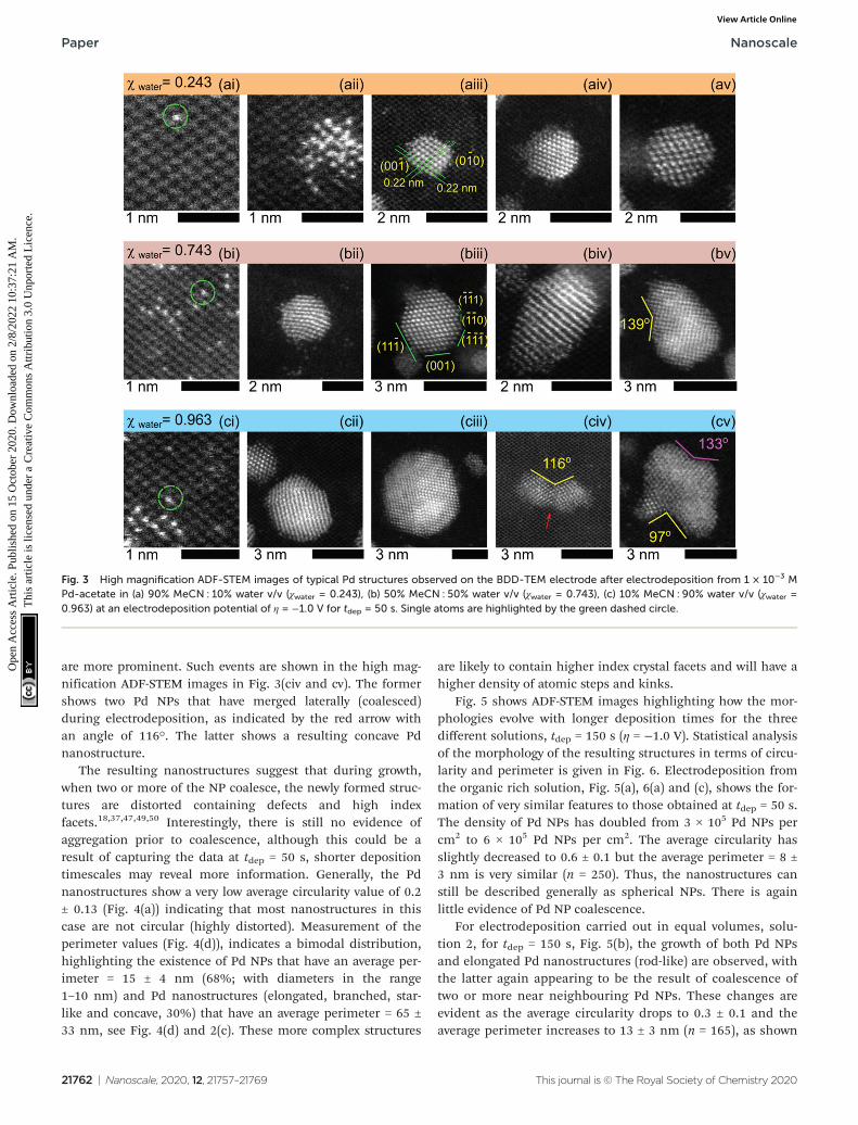
are more prominent. Such events are shown in the high mag-nification ADF-STEM images in Fig. 3(civ and cv). The formershows two Pd NPs that have merged laterally (coalesced)during electrodeposition, as indicated by the red arrow withan angle of 116°. The latter shows a resulting concave Pdnanostructure.
The resulting nanostructures suggest that during growth,when two or more of the NP coalesce, the newly formed struc-tures are distorted containing defects and high indexfacets.18,37,47,49,50 Interestingly, there is still no evidence ofaggregation prior to coalescence, although this could be aresult of capturing the data at tdep = 50 s, shorter depositiontimescales may reveal more information. Generally, the Pdnanostructures show a very low average circularity value of 0.2± 0.13 (Fig. 4(a)) indicating that most nanostructures in thiscase are not circular (highly distorted). Measurement of theperimeter values (Fig. 4(d)), indicates a bimodal distribution,highlighting the existence of Pd NPs that have an average per-imeter = 15 ± 4 nm (68%; with diameters in the range1–10 nm) and Pd nanostructures (elongated, branched, star-like and concave, 30%) that have an average perimeter = 65 ±33 nm, see Fig. 4(d) and 2(c). These more complex structures
are likely to contain higher index crystal facets and will have ahigher density of atomic steps and kinks.
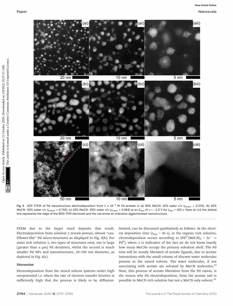
Fig. 5 shows ADF-STEM images highlighting how the mor-phologies evolve with longer deposition times for the threedifferent solutions, tdep = 150 s (η = −1.0 V). Statistical analysisof the morphology of the resulting structures in terms of circu-larity and perimeter is given in Fig. 6. Electrodeposition fromthe organic rich solution, Fig. 5(a), 6(a) and (c), shows the for-mation of very similar features to those obtained at tdep = 50 s.The density of Pd NPs has doubled from 3 × 10⁵ Pd NPs percm2 to 6 × 10⁵ Pd NPs per cm2. The average circularity hasslightly decreased to 0.6 ± 0.1 but the average perimeter = 8 ±3 nm is very similar (n = 250). Thus, the nanostructures canstill be described generally as spherical NPs. There is againlittle evidence of Pd NP coalescence.
For electrodeposition carried out in equal volumes, solu-tion 2, for tdep = 150 s, Fig. 5(b), the growth of both Pd NPsand elongated Pd nanostructures (rod-like) are observed, withthe latter again appearing to be the result of coalescence oftwo or more near neighbouring Pd NPs. These changes areevident as the average circularity drops to 0.3 ± 0.1 and theaverage perimeter increases to 13 ± 3 nm (n = 165), as shown
Fig. 3 High magnification ADF-STEM images of typical Pd structures observed on the BDD-TEM electrode after electrodeposition from 1 × 10⁻³ MPd-acetate in (a) 90% MeCN : 10% water v/v (χwater = 0.243), (b) 50% MeCN : 50% water v/v (χwater = 0.743), (c) 10% MeCN : 90% water v/v (χwater =0.963) at an electrodeposition potential of η = −1.0 V for tdep = 50 s. Single atoms are highlighted by the green dashed circle.
Paper Nanoscale
21762 | Nanoscale, 2020, 12, 21757–21769 This journal is © The Royal Society of Chemistry 2020
Ope
n A
cces
s A
rtic
le. P
ublis
hed
on 1
5 O
ctob
er 2
020.
Dow
nloa
ded
on 2
/8/2
022
10:3
7:21
AM
. T
his
artic
le is
lice
nsed
und
er a
Cre
ativ
e C
omm
ons
Attr
ibut
ion
3.0
Unp
orte
d L
icen
ce.
View Article Online
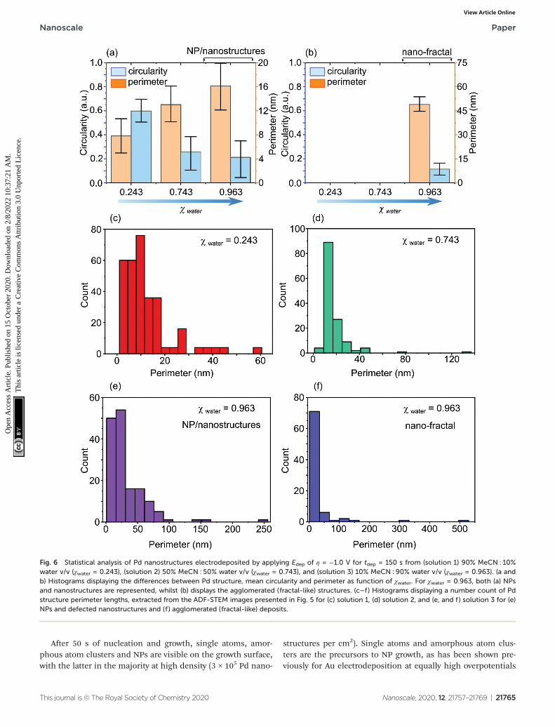
in Fig. 6(a) and (d). Electrodeposition from the water richsolution 3, is shown in Fig. 5(c) after tdep = 150 s. Under theseconditions, the most prominent feature is the growth of alarger scale interconnected porous Pd structure, producedfrom agglomerated Pd nanostructures (fractal-like mor-phology51), which appear in some cases to have coalesced(Fig. 5(cii and iii)). Much smaller Pd NP and defected Pdnanostructures are also present on the surface of BDD TEMelectrode (Fig. 5(ci)) accounting for the two different distri-butions as highlighted in Fig. 6(a), (b), (e) and (f ). The circu-larity value for these smaller Pd NPs and nanostructuresapproaches an average of 0.2 ± 0.15 with an average perimeterof 16 ± 4 nm (n = 130), i.e. the defected nanostructures aremore prominent over the NPs. For those agglomerated nano-structures that could be measured using this approach, i.e.those that are still isolated from the larger interconnectedmacrostructure, e.g. as highlighted by the red arrow in Fig. 5(ciii), an average circularity of 0.1 ± 0.05 is obtained and anaverage perimeter value of 50 ± 5 nm (n = 80). These lattervalues should serve only as a guide as these structures are
three dimensionally (3D) complex and are likely to underesti-mate the exact geometry.
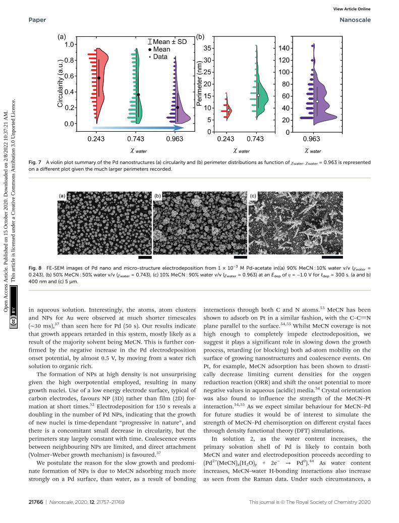
Violin plots comparing the evolution in circularity and per-imeter of the electrodeposited nanostructures as the watercontent in the mixed solvent is increased (Fig. 2, 3 and 5) arepresented in Fig. 7. Data was collated for all the analysed nano-structures for tdep = 50 s and 150 s. ESI4 Fig. S6† shows histo-grams displaying a number count of perimeter lengths for alldata collected. The black dots on Fig. 7 shows the average circu-larity or perimeter of the Pd nanostructures, for each χwater, withthe vertical line representing the mean ± standard deviation.Fig. 7 clearly shows increasing water content results in both adeviation from circularity and a favouring of the growth of mor-phologically more complex Pd nanostructures, as seen by theincreasing perimeter value and decreasing circularity values.
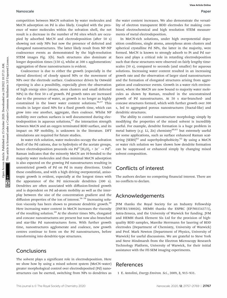
When electrodeposition was driven even longer, tdep = 300s, using the organic rich solution 1, Pd NP-like structures arestill evident, as shown by the FE-SEM images in Fig. 8(a);although at this much lower resolution it is difficult to definethe precise geometry. FE-SEM is now used in preference to
Fig. 4 Statistical analysis of Pd nanostructures obtained by electrodeposition, Edep = η = −1.0 V for tdep = 50 s in solution 1: 90% MeCN : 10% waterv/v (χwater = 0.243), solution 2: 50% MeCN : 50% water v/v (χwater = 0.743) and solution 3: 10% MeCN : 90% water v/v (χwater = 0.963). (a) Histogramdisplaying the change in Pd structure mean circularity and perimeter as function of χwater. (b–d) Histograms displaying a number count of perimeterlengths, extracted from the ADF-STEM images in Fig. 2, as a function of χwater.
Nanoscale Paper
This journal is © The Royal Society of Chemistry 2020 Nanoscale, 2020, 12, 21757–21769 | 21763
Ope
n A
cces
s A
rtic
le. P
ublis
hed
on 1
5 O
ctob
er 2
020.
Dow
nloa
ded
on 2
/8/2
022
10:3
7:21
AM
. T
his
artic
le is
lice
nsed
und
er a
Cre
ativ
e C
omm
ons
Attr
ibut
ion
3.0
Unp
orte
d L
icen
ce.
View Article Online
STEM due to the larger sized deposits that result.Electrodeposition from solution 2 reveals porous, almost “cau-liflower-like” Pd micro-structures as displayed in Fig. 8(b). Forwater rich solution 3, two types of structures exist, one is large(greater than a µm) Pd dendrites, whilst the second is muchsmaller Pd NPs and nanostructures, 20–500 nm diameter, asdepicted in Fig. 8(c).
Discussion
Electrodeposition from the mixed solvent systems under highoverpotential i.e. where the rate of electron transfer kinetics issufficiently high that the process is likely to be diffusion-
limited, can be discussed qualitatively as follows. At the short-est deposition time (tdep = 50 s), in the organic rich solution,electrodeposition occurs according to (Pd2+(MeCN)x + 2e− →Pd0), where x is indicative of the fact we do not know exactlyhow many MeCNs occupy the primary solvation shell. The Pdions will be mostly liberated of acetate ligands, due to acetateinteractions with the small volume of discrete water moleculespresent in the mixed solvent. The water molecules, if notassociating with acetate are solvated by MeCN molecules.44
Note, this process of acetate liberation from the Pd cation, isthe reason why Pd electrodeposition, from the acetate salt ispossible in MeCN rich solution but not a MeCN only solvent.44
Fig. 5 ADF-STEM of Pd nanostructure electrodeposition from 1 × 10⁻³ M Pd-acetate in (a) 90% MeCN : 10% water v/v (χwater = 0.243), (b) 50%MeCN : 50% water v/v (χwater = 0.743), (c) 10% MeCN : 90% water v/v (χwater = 0.963) at an Edep of η = −1.0 V for tdep = 150 s. Note on (ci) the dottedline represents the edge of the BDD TEM electrode and the red arrow an indicative agglomerated nanostructure.
Paper Nanoscale
21764 | Nanoscale, 2020, 12, 21757–21769 This journal is © The Royal Society of Chemistry 2020
Ope
n A
cces
s A
rtic
le. P
ublis
hed
on 1
5 O
ctob
er 2
020.
Dow
nloa
ded
on 2
/8/2
022
10:3
7:21
AM
. T
his
artic
le is
lice
nsed
und
er a
Cre
ativ
e C
omm
ons
Attr
ibut
ion
3.0
Unp
orte
d L
icen
ce.
View Article Online
After 50 s of nucleation and growth, single atoms, amor-phous atom clusters and NPs are visible on the growth surface,with the latter in the majority at high density (3 × 10⁵ Pd nano-
structures per cm2). Single atoms and amorphous atom clus-ters are the precursors to NP growth, as has been shown pre-viously for Au electrodeposition at equally high overpotentials
Fig. 6 Statistical analysis of Pd nanostructures electrodeposited by applying Edep of η = −1.0 V for tdep = 150 s from (solution 1) 90% MeCN : 10%water v/v (χwater = 0.243), (solution 2) 50% MeCN : 50% water v/v (χwater = 0.743), and (solution 3) 10% MeCN : 90% water v/v (χwater = 0.963). (a andb) Histograms displaying the differences between Pd structure, mean circularity and perimeter as function of χwater. For χwater = 0.963, both (a) NPsand nanostructures are represented, whilst (b) displays the agglomerated (fractal-like) structures. (c–f ) Histograms displaying a number count of Pdstructure perimeter lengths, extracted from the ADF-STEM images presented in Fig. 5 for (c) solution 1, (d) solution 2, and (e, and f) solution 3 for (e)NPs and defected nanostructures and (f ) agglomerated (fractal-like) deposits.
Nanoscale Paper
This journal is © The Royal Society of Chemistry 2020 Nanoscale, 2020, 12, 21757–21769 | 21765
Ope
n A
cces
s A
rtic
le. P
ublis
hed
on 1
5 O
ctob
er 2
020.
Dow
nloa
ded
on 2
/8/2
022
10:3
7:21
AM
. T
his
artic
le is
lice
nsed
und
er a
Cre
ativ
e C
omm
ons
Attr
ibut
ion
3.0
Unp
orte
d L
icen
ce.
View Article Online
in aqueous solution. Interestingly, the atoms, atom clustersand NPs for Au were observed at much shorter timescales(∼30 ms),37 than seen here for Pd (50 s). Our results indicatethat growth appears retarded in this system, mostly likely as aresult of the majority solvent being MeCN. This is further con-firmed by the negative increase in the Pd electrodepositiononset potential, by almost 0.5 V, by moving from a water richsolution to organic rich.
The formation of NPs at high density is not unsurprisinggiven the high overpotential employed, resulting in manygrowth nuclei. Use of a low energy electrode surface, typical ofcarbon electrodes, favours NP (3D) rather than film (2D) for-mation at short times.52 Electrodeposition for 150 s reveals adoubling in the number of Pd NPs, indicating that the growthof new nuclei is time-dependant “progressive in nature”, andthere is a concomitant small decrease in circularity, but theperimeters stay largely constant with time. Coalescence eventsbetween neighbouring NPs are limited, and direct attachment(Volmer–Weber growth mechanism) is favoured.37
We postulate the reason for the slow growth and predomi-nate formation of NPs is due to MeCN adsorbing much morestrongly on a Pd surface, than water, as a result of bonding
interactions through both C and N atoms.53 MeCN has beenshown to adsorb on Pt in a similar fashion, with the C–CuNplane parallel to the surface.54,55 Whilst MeCN coverage is nothigh enough to completely impede electrodeposition, wesuggest it plays a significant role in slowing down the growthprocess, retarding (or blocking) both ad-atom mobility on thesurface of growing nanostructures and coalescence events. OnPt, for example, MeCN adsorption has been shown to drasti-cally decrease limiting current densities for the oxygenreduction reaction (ORR) and shift the onset potential to morenegative values in aqueous (acidic) media.54 Crystal orientationwas also found to influence the strength of the MeCN–Ptinteraction.54,55 As we expect similar behaviour for MeCN–Pdfor future studies it would be of interest to simulate thestrength of MeCN–Pd chemisorption on different crystal facesthrough density functional theory (DFT) simulations.
In solution 2, as the water content increases, theprimary solvation shell of Pd is likely to contain bothMeCN and water and electrodeposition proceeds according to(Pd2+(MeCN)x(H2O)y + 2e− → Pd0).44 As water contentincreases, MeCN–water H-bonding interactions also increaseas seen from the Raman data. Under such circumstances, a
Fig. 7 A violin plot summary of the Pd nanostructures (a) circularity and (b) perimeter distributions as function of χwater. χwater = 0.963 is representedon a different plot given the much larger perimeters recorded.
Fig. 8 FE-SEM images of Pd nano and micro-structure electrodeposition from 1 × 10⁻³ M Pd-acetate in((a) 90% MeCN : 10% water v/v (χwater =0.243), (b) 50% MeCN : 50% water v/v (χwater = 0.743), (c) 10% MeCN : 90% water v/v (χwater = 0.963) at an Edep of η = −1.0 V for tdep = 300 s. (a and b)400 nm and (c) 5 µm.
Paper Nanoscale
21766 | Nanoscale, 2020, 12, 21757–21769 This journal is © The Royal Society of Chemistry 2020
Ope
n A
cces
s A
rtic
le. P
ublis
hed
on 1
5 O
ctob
er 2
020.
Dow
nloa
ded
on 2
/8/2
022
10:3
7:21
AM
. T
his
artic
le is
lice
nsed
und
er a
Cre
ativ
e C
omm
ons
Attr
ibut
ion
3.0
Unp
orte
d L
icen
ce.
View Article Online
competition between MeCN solvation by water molecules andMeCN adsorption on Pd is also likely. Coupled with the pres-ence of water molecules within the solvation shell, the netresult is a decrease in the number of Pd sites which are occu-pied by adsorbed MeCN and electrodeposition (after 50 s)showing not only NPs but now the presence of defected andelongated nanostructures. The latter likely result from NP–NPcoalescence events as demonstrated by the high-resolutionSTEM images Fig. 3(b). Such structures also dominate atlonger deposition times (150 s), whilst at 300 s agglomeration/aggregation of these nanostructures is evident.
Coalescence is due to either the growth (especially in thelateral direction) of closely spaced NPs or the movement ofNPs over the electrode surface. Coalescence driven by Ostwaldripening is also a possibility, especially given the observationof high energy sites (atoms, atom clusters and small defectedNPs) in the first 50 s of growth. Pd growth rates are increaseddue to the presence of water, as growth is no longer as highlyconstrained in the lower water content solutions.56,57 Thisresults in larger sized NPs for a fixed growth time, which cangrow into one another, aggregate, then coalesce. Whilst NPmobility over carbon surfaces is well documented during elec-trodeposition in aqueous solutions,47 the interaction strengthbetween MeCN and an oxygen terminated BDD surface, and itsimpact on NP mobility, is unknown in the literature. DFTsimulations are required for future studies.
In water rich solution, water molecules occupy the solvationshell of the Pd cations, due to hydrolysis of the acetate groups,hence electrodeposition proceeds via Pd2+(H2O)y + 2e− → Pd0.Raman indicates that the minority MeCN are H-bonded to themajority water molecules and thus minimal MeCN adsorptionis also expected on the growing Pd nanostructures resulting inunrestricted growth of Pd on Pd in many directions. Underthese conditions, and with a high driving overpotential, aniso-tropic growth is evident, especially at the longest times withthe appearance of the Pd microscale dendrites (300 s).Dendrites are often associated with diffusion-limited growthand is dependent on Pd ad-atom mobility as well as the inter-play between the size of the concentration gradient and thediffusion properties of the ion of interest.56–58 Increasing solu-tion viscosity has been shown to promote dendritic growth.58
Here increasing water content in MeCN increases the viscosityof the resulting solution.59 At the shorter times NPs, elongatedand concave nanostructures are present but now also branchedand star-like Pd nanostructures form. With further growthtime, nanostructures agglomerate and coalesce, new growthcentres continue to form on the Pd nanostructures, beforetransforming into dendritic-type structures.
Conclusions
The solvent plays a significant role in electrodeposition. Herewe show how by using a mixed solvent system (MeCN–water)greater morphological control over electrodeposited (Pd) nano-structures can be exerted, switching from NPs to dendrites as
the water content increases. We also demonstrate the versati-lity of electron transparent BDD electrodes for making com-bined electrochemical and high resolution STEM measure-ments of metal electrodeposition.
In MeCN-rich solutions, under high overpotential depo-sition conditions, single atoms, amorphous atom clusters andspherical crystalline Pd NPs, the latter in the majority, wereformed. MeCN is known to strongly adsorb to Pt and Pd sur-faces and plays a critical role in retarding electrodepositionsuch that these structures were observed on fairly lengthy time-scales (50 s), compared to seconds (and smaller) for aqueoussolutions. Increasing water content resulted in an increasinggrowth rate and the observation of larger sized nanostructuresand the formation of elongated structures arising from aggre-gation and coalescence events. Growth in a water rich environ-ment, where the MeCN are now bound to majority water mole-cules as shown by Raman, resulted in the unconstrainedgrowth of Pd nanostructures. At 50 s star-branched- andconcave structures formed, which with further growth over 300s, led to aggregated porous nanostructures (fractal-like) anddendritic structures.
The ability to control nanostructure morphology simply bymodifying the properties of the mixed solvent is incrediblyuseful. For example, dendrite formation is a huge problem inmetal battery (e.g. Li, Zn) chemistry60,61 but extremely usefulfor some applications, such as surface enhanced Raman scat-tering (SERS)62 and superhydrophobicity.62 By using a MeCNor water rich solution we have shown how dendrite formationcan be suppressed or enhanced simply by changing mixedsolvent composition.
Conflicts of interest
The authors declare no competing financial interest. There areno conflicts to declare.
Acknowledgements
JVM thanks the Royal Society for an Industry Fellowship(INF/R1/180026). HEMH thanks the ESPRC (EP/N035437/1),Astra-Zeneca, and the University of Warwick for funding. JVMand HEMH thank Element Six Ltd for the provision of high-quality BDD samples, Mareike Herrmann for lasering of BDDelectrodes (Department of Chemistry, University of Warwick)and Prof. Mark Newton (Department of Physics, University ofWarwick) for useful discussions. We are grateful to Steve Yorkand Steve Hindmarsh from the Electron Microscopy ResearchTechnology Platform, University of Warwick, for their initialassistance with the FE-SEM imaging experiments.
References
1 E. Antolini, Energy Environ. Sci., 2009, 2, 915–931.
Nanoscale Paper
This journal is © The Royal Society of Chemistry 2020 Nanoscale, 2020, 12, 21757–21769 | 21767
Ope
n A
cces
s A
rtic
le. P
ublis
hed
on 1
5 O
ctob
er 2
020.
Dow
nloa
ded
on 2
/8/2
022
10:3
7:21
AM
. T
his
artic
le is
lice
nsed
und
er a
Cre
ativ
e C
omm
ons
Attr
ibut
ion
3.0
Unp
orte
d L
icen
ce.
View Article Online
2 F. Yang, K. Cheng, T. Wu, Y. Zhang, J. Yin, G. Wang andD. Cao, Electrochim. Acta, 2013, 99, 54–61.
3 M. Luo and S. Guo, Nat. Rev. Mater., 2017, 2, 17059.4 A. R. Poerwoprajitno, L. O. Gloag, S. Cheong, J. J. Gooding
and R. Tilley, Nanoscale, 2019, 18995–19011.5 S. Mukerjee, S. Srinivasan, M. P. Soriaga and J. McBreen,
J. Electrochem. Soc., 1995, 142, 1409–1422.6 N. P. Lebedeva, M. T. M. Koper, J. M. Feliu and R. A. Van
Santen, J. Phys. Chem. B, 2002, 106, 12938.7 P. Allongue and F. Maroun, Curr. Opin. Solid State Mater.
Sci., 2006, 10, 173–181.8 N. Tian, Z.-Y. Zhou and S.-G. Sun, J. Phys. Chem. C, 2008,
112, 19801–19817.9 K. Zhou and Y. Li, Angew. Chem., Int. Ed., 2012, 51, 602–
613.10 J. Kim, J. E. Dick and A. J. Bard, Acc. Chem. Res., 2016, 49,
2587–2595.11 N. Tian, Z.-Y. Zhou, N.-F. Yu, L.-Y. Wang and S.-G. Sun,
J. Am. Chem. Soc., 2010, 132, 7580–7581.12 S. T. Christensen, J. W. Elam, F. A. Rabuffetti, Q. Ma,
S. J. Weigand, B. Lee, S. Seifert, P. C. Stair,K. R. Poeppelmeier, M. C. Hersam and M. J. Bedzyk, Small,2009, 5, 750–757.
13 D. M. Kolb, R. Ullmann and T. Will, Science, 1997, 275,1097–1099.
14 A. Gharachorlou, M. D. Detwiler, A. V. Nartova, Y. Lei, J. Lu,J. W. Elam, W. N. Delgass, F. H. Ribeiro andD. Y. Zemlyanov, ACS Appl. Mater. Interfaces, 2014, 6,14702–14711.
15 M. P. Pileni, Acc. Chem. Res., 2012, 45, 1965–1972.16 J. J. Willis, E. D. Goodman, L. Wu, A. R. Riscoe, P. Martins,
C. J. Tassone and M. Cargnello, J. Am. Chem. Soc., 2017,139, 11989–11997.
17 F. Favier, E. C. Walter, M. P. Zach, T. Benter andR. M. Penner, Science, 2001, 293, 2227–2231.
18 J. Ustarroz, J. A. Hammons, T. Altantzis, A. Hubin, S. Balsand H. Terryn, J. Am. Chem. Soc., 2013, 135, 11550–11561.
19 P. N. Bartlett, P. R. Birkin and M. A. Ghanem, Chem.Commun., 2000, 1671–1672.
20 P. N. Bartlett, B. Gollas, S. Guerin and J. Marwan, Phys.Chem. Chem. Phys., 2002, 4, 3835–3842.
21 R. M. Penner, M. J. Heben, T. L. Longin and N. S. Lewis,Science, 1990, 250, 1118–1121.
22 D. J. Riley, Curr. Opin. Colloid Interface Sci., 2002, 7, 186–192.
23 T. Takei, Surf. Technol., 1979, 8, 543–552.24 M. Fleischmann, S. Pons, J. Sousa and J. Ghoroghchian,
J. Electroanal. Chem., 1994, 366, 171–190.25 A. Mourato, J. P. Correia, H. Siegenthaler and
L. M. Abrantes, Electrochim. Acta, 2007, 53, 664–672.26 L. P. Bicelli, B. Bozzini, C. Mele and L. D’Urzo,
Int. J. Electrochem. Sci., 2008, 3, 356–408.27 Z.-Y. Zhou, N. Tian, Z.-Z. Huang, D.-J. Chen and S.-G. Sun,
Faraday Discuss., 2009, 140, 81–92.28 Z. Quan, Y. Wang and J. Fang, Acc. Chem. Res., 2013, 46,
191–202.
29 M. Jin, H. Zhang, Z. Xie and Y. Xia, Angew. Chem., Int. Ed.,2011, 50, 7850–7854.
30 F. Fu and Q. Wang, J. Environ. Manage., 2011, 92, 407–418.
31 C. Mele, S. Rondinini, L. D’Urzo, V. Romanello, E. Tondo,A. Minguzzi, A. Vertova and B. Bozzini, J. Solid StateElectrochem., 2009, 13, 1577–1584.
32 H. Gerischer, Electrochemical Reactions in Nonaqueous andMixed Solvents, 1990.
33 K. Izutsu, Electrochemistry in nonaqueous solutions, Wiley-VCH Verlag GmbH & Co. KGaA, Weinheim, 2009.
34 H. L. Yu, J. N. Zhao, L. B. Ben, Y. J. Zhan, Y. D. Wuand X. J. Huang, ACS Energy Lett., 2017, 2, 1296–1302.
35 N. Dubouis, A. Serva, E. Salager, M. Deschamps,M. Salanne and A. Grimaud, J. Phys. Chem. Lett., 2018, 9,6683–6688.
36 C. Ma, A. Laaksonen, C. Liu, X. Lu and X. Ji, Chem. Soc.Rev., 2018, 47, 8685–8720.
37 H. E. M. Hussein, R. J. Maurer, H. Amari, J. J. P. Peters,L. Meng, R. Beanland, M. E. Newton and J. V. Macpherson,ACS Nano, 2018, 12, 7388–7396.
38 J. R. Reimers and L. E. Hall, J. Am. Chem. Soc., 1999, 121,3730–3744.
39 L. D. Supran and N. Sheppard, Chem. Commun., 1967, 832–834.
40 E. Venardou, E. Garcia-Verdugo, S. J. Barlow,Y. E. Gorbaty and M. Poliakoff, Vib. Spectrosc., 2004, 35,103–109.
41 B. G. Cox, G. R. Hedwig, A. J. Parker and D. W. Watts,Aust. J. Chem., 1974, 27, 477–501.
42 D. Jamroz, J. Stangret and J. Lindgren, J. Am. Chem. Soc.,1993, 115, 6165–6168.
43 J. M. Alía and H. G. M. Edwards, Vib. Spectrosc., 2004, 34,225–230.
44 H. E. M. Hussein, A. D. Ray and J. V. Macpherson, GreenChem., 2019, 21, 4662–4672.
45 C. A. Schneider, W. S. Rasband and K. W. Eliceiri, Nat.Methods, 2012, 9, 671–675.
46 J. Ustarroz, U. Gupta, A. Hubin, S. Bals and H. Terryn,Electrochem. Commun., 2010, 12, 1706–1709.
47 J. Ustarroz, X. Ke, A. Hubin, S. Bals and H. Terryn, J. Phys.Chem. C, 2012, 116, 2322–2329.
48 J. Ustarroz, T. Altantzis, J. A. Hammons, A. Hubin,S. Bals and H. Terryn, Chem. Mater., 2014, 26, 2396–2406.
49 H. E. M. Hussein, H. Amari and J. V. Macpherson, ACSCatal., 2017, 7, 7388–7398.
50 J. Ustarroz, J. A. Hammons, Y. Van Ingelgem, M. Tzedaki,A. Hubin and H. Terryn, Electrochem. Commun., 2011, 13,1320–1323.
51 A. Ghosh, R. Batabyal, G. P. Das and B. N. Dev, AIP Adv.,2016, 6, 015301-1–015301-12.
52 R. M. Penner, in Handbook of Electrochemistry, ed.C. G. Zoski, Elsevier, Amsterdam, 2007, pp. 661–677.
53 K. Kosaku and I. Shigero, Surf. Sci., 1981, 107, 405–416.
Paper Nanoscale
21768 | Nanoscale, 2020, 12, 21757–21769 This journal is © The Royal Society of Chemistry 2020
Ope
n A
cces
s A
rtic
le. P
ublis
hed
on 1
5 O
ctob
er 2
020.
Dow
nloa
ded
on 2
/8/2
022
10:3
7:21
AM
. T
his
artic
le is
lice
nsed
und
er a
Cre
ativ
e C
omm
ons
Attr
ibut
ion
3.0
Unp
orte
d L
icen
ce.
View Article Online
54 V. Briega-Martos, M. Costa-Figueiredo, J. M. Orts, A. Rodes,M. T. M. Koper, E. Herrero and J. M. Feliu, J. Phys. Chem. C,2019, 123, 2300–2313.
55 G. S. Harlow, I. M. Aldous, P. Thompson, Y. Grunder,L. J. Hardwick and C. A. Lucas, Phys. Chem. Chem. Phys.,2019, 21, 8654–8662.
56 D. K. Sharma, A. Ott, A. P. O’Mullane and S. K. Bhargava,Colloids Surf., A, 2011, 386, 98–106.
57 D. Torres, L. Madriz, R. Vargas and B. R. Scharifker,Electrochim. Acta, 2020, 354, 136705-1–136705-9.
58 W. Liu, T. Yang, J. Liu, P. Che and Y. Han, Ind. Eng. Chem.Res., 2016, 55, 8319–8326.
59 J. W. Thompson, T. J. Kaiser and J. W. Jorgenson,J. Chromatogr., A, 2006, 1134, 201–209.
60 F. Hao, A. Verma and P. P. Mukherjee, ACS Appl. Mater.Interfaces, 2018, 10, 26320–26327.
61 S. J. Banik and R. Akolkar, J. Electrochem. Soc., 2013, 160,D519–D523.
62 G. Lu, C. Li and G. Shi, Chem. Mater., 2007, 19,3433–3440.
Nanoscale Paper
This journal is © The Royal Society of Chemistry 2020 Nanoscale, 2020, 12, 21757–21769 | 21769
Ope
n A
cces
s A
rtic
le. P
ublis
hed
on 1
5 O
ctob
er 2
020.
Dow
nloa
ded
on 2
/8/2
022
10:3
7:21
AM
. T
his
artic
le is
lice
nsed
und
er a
Cre
ativ
e C
omm
ons
Attr
ibut
ion
3.0
Unp
orte
d L
icen
ce.
View Article Online


![Electrodeposition of Zn-Mn alloys from recycling battery leach … · 2014. 5. 20. · recovery by electrodeposition [1–4] is currently being studied in our laboratory [5]. Electrodeposition](https://img.pdfslide.us/doc/110x75/6112e3e4b1654c15ca54266d/electrodeposition-of-zn-mn-alloys-from-recycling-battery-leach-2014-5-20-recovery.jpg)

![Electrodeposition of palladium on the copper lead frame ... · between palladium ions and additives to gain good qualities in elec-trodeposition [3]. Thus more additives were added](https://img.pdfslide.us/doc/110x75/5e72c2a7bb8a8878af60a42b/electrodeposition-of-palladium-on-the-copper-lead-frame-between-palladium-ions.jpg)