Embed Size (px)
Citation preview
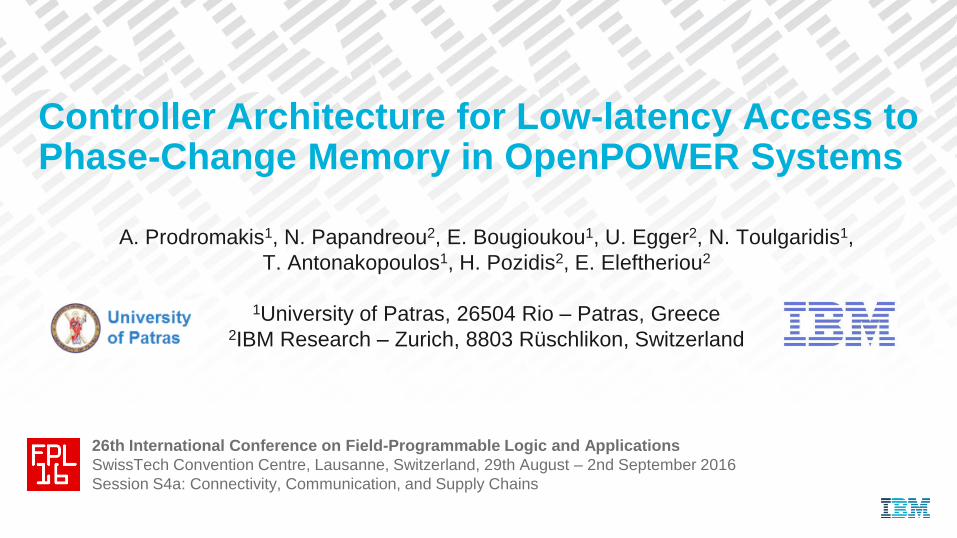
Controller Architecture for Low-latency Access to Phase-Change Memory in OpenPOWER Systems
A. Prodromakis1, N. Papandreou2, E. Bougioukou1, U. Egger2, N. Toulgaridis1,
T. Antonakopoulos1, H. Pozidis2, E. Eleftheriou2
1University of Patras, 26504 Rio – Patras, Greece
2IBM Research – Zurich, 8803 Rüschlikon, Switzerland
26th International Conference on Field-Programmable Logic and Applications
SwissTech Convention Centre, Lausanne, Switzerland, 29th August – 2nd September 2016
Session S4a: Connectivity, Communication, and Supply Chains
26th International Conference on Field Programmable Logic and Applications (FPL 2016)
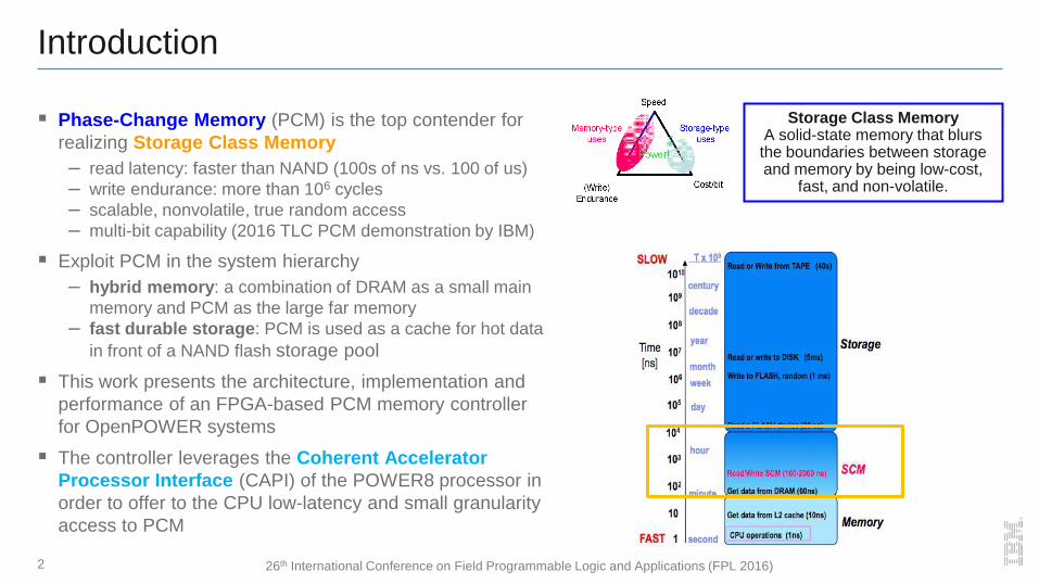
Introduction
Phase-Change Memory (PCM) is the top contender for
realizing Storage Class Memory
– read latency: faster than NAND (100s of ns vs. 100 of us)
– write endurance: more than 106 cycles
– scalable, nonvolatile, true random access
– multi-bit capability (2016 TLC PCM demonstration by IBM)
Exploit PCM in the system hierarchy
– hybrid memory: a combination of DRAM as a small main
memory and PCM as the large far memory
– fast durable storage: PCM is used as a cache for hot data
in front of a NAND flash storage pool
This work presents the architecture, implementation and
performance of an FPGA-based PCM memory controller
for OpenPOWER systems
The controller leverages the Coherent Accelerator
Processor Interface (CAPI) of the POWER8 processor in
order to offer to the CPU low-latency and small granularity
access to PCM
2
Storage Class Memory A solid-state memory that blurs the boundaries between storage and memory by being low-cost,
fast, and non-volatile.
26th International Conference on Field Programmable Logic and Applications (FPL 2016)
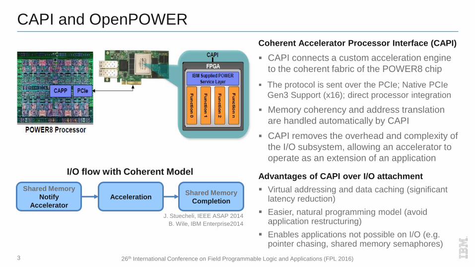
CAPI and OpenPOWER
3
I/O flow with Coherent Model
Shared Memory
Notify
Accelerator
Acceleration Shared Memory
Completion
Coherent Accelerator Processor Interface (CAPI)
CAPI connects a custom acceleration engine
to the coherent fabric of the POWER8 chip
The protocol is sent over the PCIe; Native PCIe
Gen3 Support (x16); direct processor integration
Memory coherency and address translation
are handled automatically by CAPI
CAPI removes the overhead and complexity of
the I/O subsystem, allowing an accelerator to
operate as an extension of an application
Advantages of CAPI over I/O attachment
Virtual addressing and data caching (significant latency reduction)
Easier, natural programming model (avoid application restructuring)
Enables applications not possible on I/O (e.g. pointer chasing, shared memory semaphores)
J. Stuecheli, IEEE ASAP 2014
B. Wile, IBM Enterprise2014
26th International Conference on Field Programmable Logic and Applications (FPL 2016)
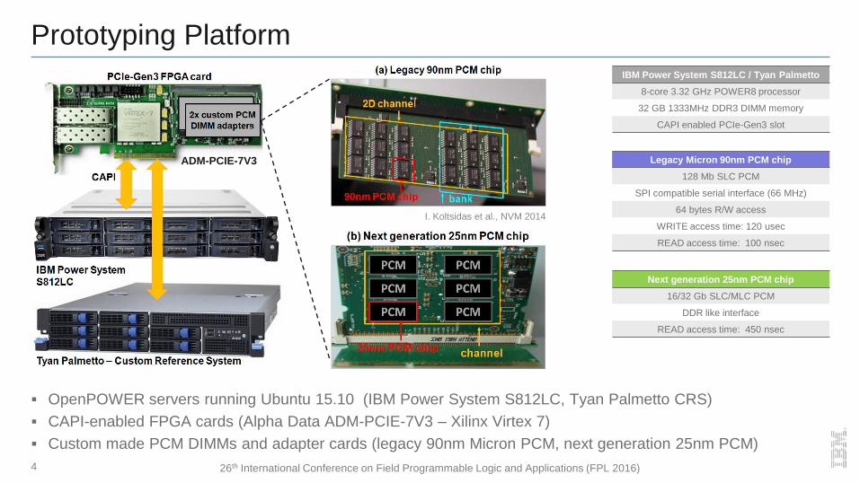
Legacy Micron 90nm PCM chip
128 Mb SLC PCM
SPI compatible serial interface (66 MHz)
64 bytes R/W access
WRITE access time: 120 usec
READ access time: 100 nsec
Prototyping Platform
4
OpenPOWER servers running Ubuntu 15.10 (IBM Power System S812LC, Tyan Palmetto CRS)
CAPI-enabled FPGA cards (Alpha Data ADM-PCIE-7V3 – Xilinx Virtex 7)
Custom made PCM DIMMs and adapter cards (legacy 90nm Micron PCM, next generation 25nm PCM)
IBM Power System S812LC / Tyan Palmetto
8-core 3.32 GHz POWER8 processor
32 GB 1333MHz DDR3 DIMM memory
CAPI enabled PCIe-Gen3 slot
Next generation 25nm PCM chip
16/32 Gb SLC/MLC PCM
DDR like interface
READ access time: 450 nsec
ADM-PCIE-7V3
I. Koltsidas et al., NVM 2014
26th International Conference on Field Programmable Logic and Applications (FPL 2016)
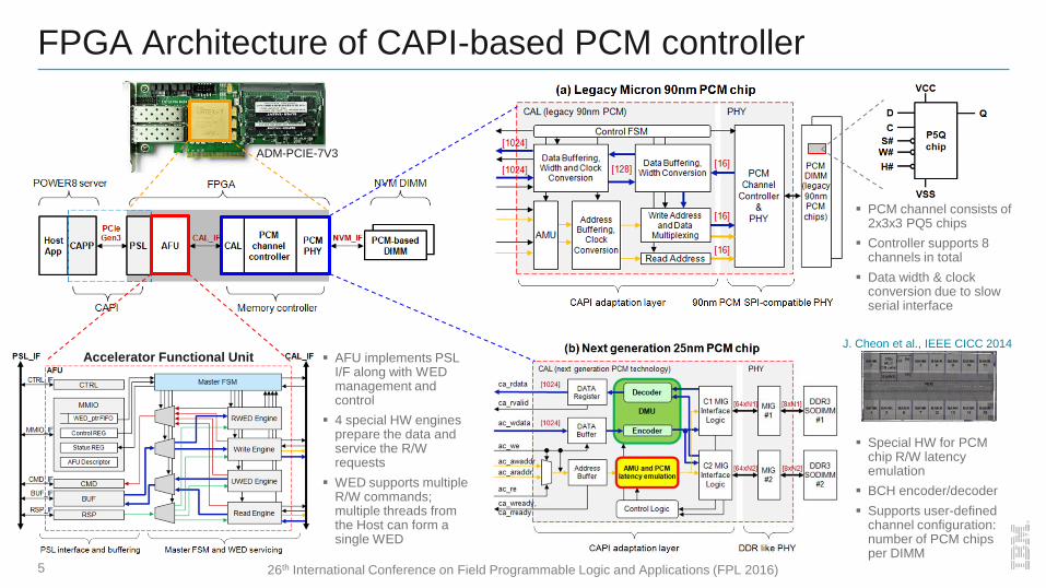
FPGA Architecture of CAPI-based PCM controller
5
AFU implements PSL I/F along with WED management and control
4 special HW engines prepare the data and service the R/W requests
WED supports multiple R/W commands; multiple threads from the Host can form a single WED
PCM channel consists of 2x3x3 PQ5 chips
Controller supports 8 channels in total
Data width & clock conversion due to slow serial interface
Special HW for PCM chip R/W latency emulation
BCH encoder/decoder
Supports user-defined channel configuration: number of PCM chips per DIMM
J. Cheon et al., IEEE CICC 2014
Accelerator Functional Unit
ADM-PCIE-7V3
26th International Conference on Field Programmable Logic and Applications (FPL 2016)
Performance results
6
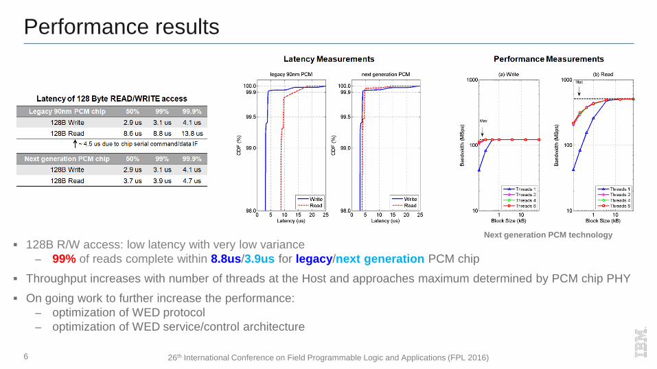
128B R/W access: low latency with very low variance
– 99% of reads complete within 8.8us/3.9us for legacy/next generation PCM chip
Throughput increases with number of threads at the Host and approaches maximum determined by PCM chip PHY
On going work to further increase the performance:
– optimization of WED protocol
– optimization of WED service/control architecture
Next generation PCM technology
26th International Conference on Field Programmable Logic and Applications (FPL 2016)
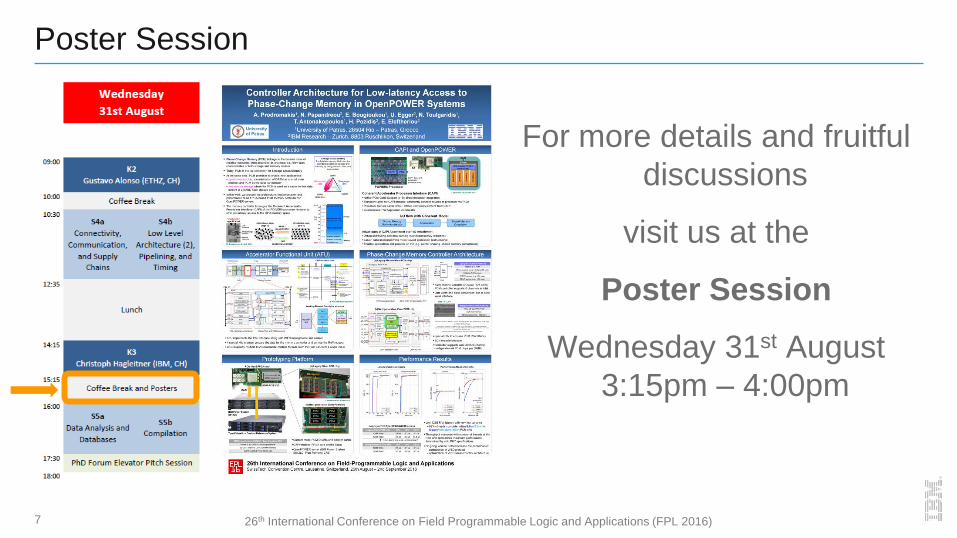
Poster Session
7
For more details and fruitful
discussions
visit us at the
Poster Session
Wednesday 31st August
3:15pm – 4:00pm