Embed Size (px)
Citation preview
KDK COLLEGE OF ENGINEERING, NAGPUR
Control system-II Lecture Notes Subject Code: BEELE701T
For 7th Sem. Electrical Engineering Student
DEPARTMENT OF ELECTRICAL ENGINEERING
2
BEELE701T – CONTROL
SYSTEMS -II Learning Objectives Learning Outcomes
To impart knowledge of classical
controller/compensator design for linear
systems.
To understand the theory and analyze non-
linear system.
To have idea about optimal and discrete time
control system.
Students will be able to
• Analyze the practical system for the desired specifications through
classical and state variable approach.
• Design the optimal control with and without constraints
• Analyze non-linear and work with digital system and their further
research.
UNIT - I
COMPENSATION: Need for compensation. Performance Analysis of Lead, Lag and Lag-
lead Compensators in time & frequency domain, Bode Plots of Lead, Lag and Lag-lead
Compensators. (Design of Compensator is not required).
UNIT-II
Solution of state equation: Review of state variable representations , diagonalization of
state model ,eigen values and eigen vectors , generalized eigen vector, properties of state
transition matrix (STM) , Computation of STM by Laplace transform, Cayley Hamilton
theorem and Canonical transformation method. Solution of state equation.
UNIT-III
Design by state variable feedback: Controllability & observability. Kalman’s test and
Gilbert’s test, duality, Design of State variable feedback. Effect of state feedback on
controllability and observability.
UNIT-IV
Optimal Control System: Performance Index. Desirability of single P.I. Integral Square
Error (ISE), Parseval’s Theorem, parameter Optimization with & without constraints.
Optimal control problem with T.F. approach for continuous time system only.
UNIT - V
Non Linear Control Systems: Types of non - linearities. jump resonance. Describing
function analysis and its assumptions. Describing function of some common non-
linearities. Singular points. Stability from nature of singular points. Limit cycles. Isocline
method, Delta method.(Construction of phase trajectories is not expected)
UN1T-VI
Sampled Data Control Systems: Representation SDCS. Sampler & Hold circuit. Shanon’s
Sampling theorem, Z- Transform. Inverse Z- Transform & solution of Differencial
Equations. 'Z' & 'S' domain relationship. Stability by Bi- linear transformation & Jury's test.
Controllability &. observability of Discrete time systems.
BOOKS :
Text Books
Title of Book Name of Author/s Edition & Publisher
Control System Analysis Nagrath & Gopal New Age International
Linear Control System Analysis
and Design
Constantine H. Houpis, Stuart N. Sheldon,
John J. D'Azzo, Constantine H. Houpis, Stuart N. Sheldon
CRC Press
Digital Control and state variable methods
M. Gopal The McGraw-Hill
Reference Books
Modern Control Engineering k. Ogata Prentice Hall
Modern control system M.Gopal New Age International
Modern Control Engineering D.Roy Choudhury PHI Learning Private Limited, New Delhi
3
UNIT - I
COMPENSATION
Compensator is an additional component or circuit that is inserted into a control system to
equalize or compensate for a deficient performance.
Necessities of compensation
1. In order to obtain the desired performance of the system, we use compensating networks.
Compensating networks are applied to the system in the form of feed forward path gain
adjustment.
2. Compensate a unstable system to make it stable.
3. A compensating network is used to minimize overshoot.
4. These compensating networks increase the steady state accuracy of the system. An
important point to be noted here is that the increase in the steady state accuracy brings
instability to the system.
5. Compensating networks also introduces poles and zeros in the system thereby causes
changes in the transfer function of the system. Due to this, performance specifications of
the system change.
Types of Compensator.
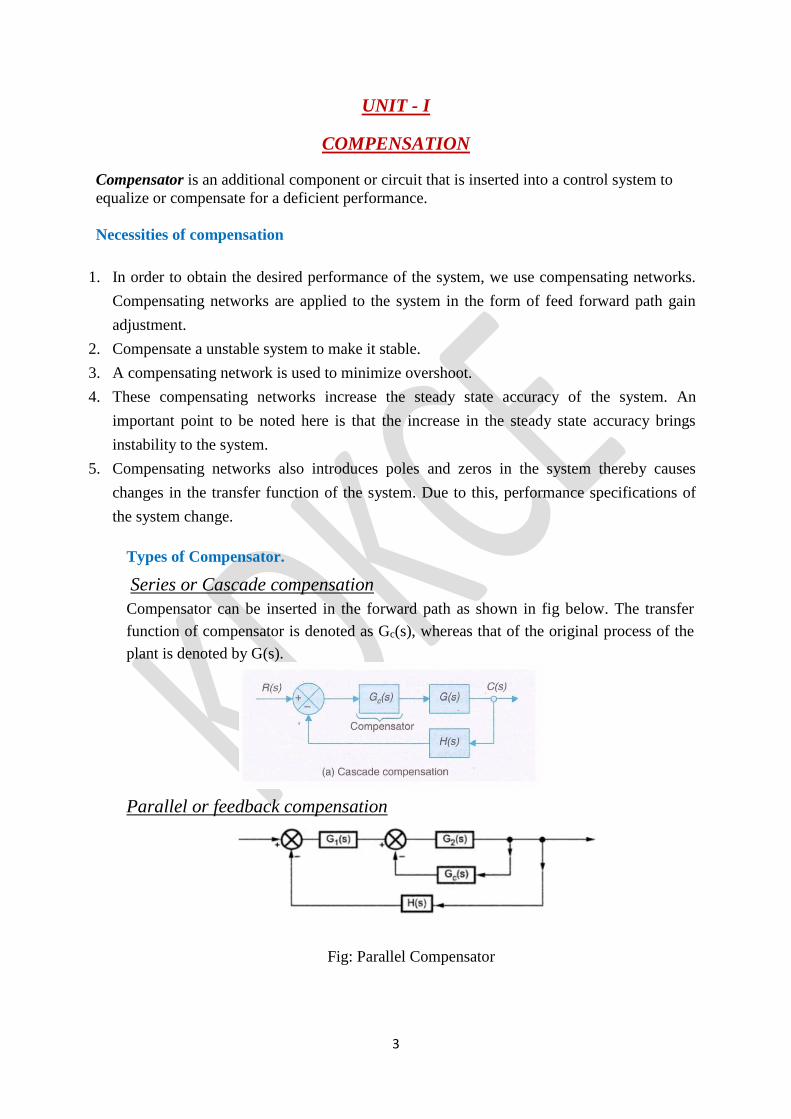
Series or Cascade compensation
Compensator can be inserted in the forward path as shown in fig below. The transfer
function of compensator is denoted as Gc(s), whereas that of the original process of the
plant is denoted by G(s).
Parallel or feedback compensation
Fig: Parallel Compensator
4
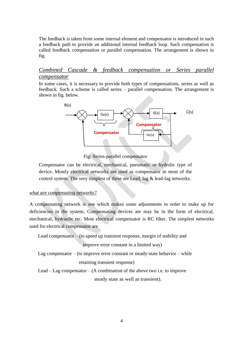
The feedback is taken from some internal element and compensator is introduced in such
a feedback path to provide an additional internal feedback loop. Such compensation is
called feedback compensation or parallel compensation. The arrangement is shown in
fig.
Combined Cascade & feedback compensation or Series parallel
compensator
In some cases, it is necessary to provide both types of compensations, series as well as
feedback. Such a scheme is called series – parallel compensation. The arrangement is
shown in fig. below.
Fig: Series-parallel compensator
Compensator can be electrical, mechanical, pneumatic or hydrolic type of
device. Mostly electrical networks are used as compensator in most of the
control system. The very simplest of these are Lead, lag & lead-lag networks.
what are compensating networks?
A compensating network is one which makes some adjustments in order to make up for
deficiencies in the system. Compensating devices are may be in the form of electrical,
mechanical, hydraulic etc. Most electrical compensator is RC filter. The simplest networks
used for electrical compensator are
Lead compensator – (to speed up transient response, margin of stability and
improve error constant in a limited way)
Lag compensator – (to improve error constant or steady-state behavior – while
retaining transient response)
Lead – Lag compensator – (A combination of the above two i.e. to improve
steady state as well as transient).
G(s)
Hc(s)
C(s)
R(s)
Ge(s)
Compensator
Compensator
5
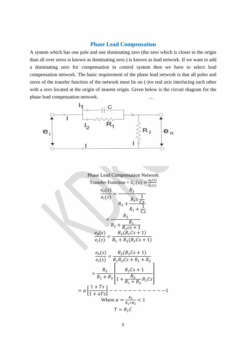
Phase Lead Compensation
A system which has one pole and one dominating zero (the zero which is closer to the origin
than all over zeros is known as dominating zero.) is known as lead network. If we want to add
a dominating zero for compensation in control system then we have to select lead
compensation network. The basic requirement of the phase lead network is that all poles and
zeros of the transfer function of the network must lie on (-)ve real axis interlacing each other
with a zero located at the origin of nearest origin. Given below is the circuit diagram for the
phase lead compensation network.
Phase Lead Compensation Network
Transfer Function = 𝐺𝑐(𝑠) =𝑒0(𝑠)
𝑒𝑖(𝑠)
𝑒0(𝑠)
𝑒𝑖(𝑠)=
𝑅2
𝑅2 +𝑅1𝑥
1𝐶𝑠
𝑅1 +1
𝐶𝑠
=𝑅2
𝑅2 +𝑅1
𝑅1𝑐𝑠 + 1
𝑒0(𝑠)
𝑒𝑖(𝑠)=
𝑅2(𝑅1𝐶𝑠 + 1)
𝑅1 + 𝑅2(𝑅1𝐶𝑠 + 1)
𝑒0(𝑠)
𝑒𝑖(𝑠)=
𝑅2(𝑅1𝐶𝑠 + 1)
𝑅1𝑅2𝐶𝑠 + 𝑅1 + 𝑅2
=𝑅2
𝑅1 + 𝑅2[
𝑅1𝐶𝑠 + 1
1 +𝑅2
𝑅1 + 𝑅2𝑅1𝐶𝑠
]
= 𝛼 [1 + 𝑇𝑠
1 + 𝛼𝑇𝑠] − − − − − − − − − − − −1
Where 𝛼 =𝑅2
𝑅1+𝑅2< 1
𝑇 = 𝑅1𝐶
6
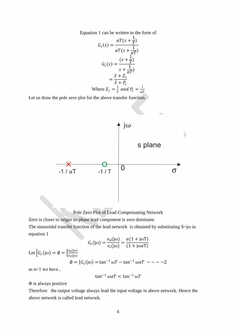
Equation 1 can be written in the form of
𝐺𝑐(𝑠) =𝛼𝑇(𝑠 +
1𝑇)
𝛼𝑇(𝑠 +1
𝛼𝑇)
𝐺𝑐(𝑠) =(𝑠 +
1𝑇)
𝑠 +1
𝛼𝑇)
=𝑆 + 𝑍𝑐
𝑆 + 𝑃𝑐
Where 𝑍𝑐 =1
𝑇 𝑎𝑛𝑑 𝑃𝑐 =
1
𝛼𝑇
Let us draw the pole zero plot for the above transfer function.
Pole Zero Plot of Lead Compensating Network
Zero is closer to origin so phase lead component is zero dominant.
The sinusoidal transfer function of the lead network is obtained by substituting S=jω in
equation 1
𝐺𝑐(jω) =𝑒0(jω)
𝑒𝑖(jω)=
𝛼(1 + jωT)
(1 + jωαT)
Let ⌊𝐺𝑐(jω) = ∅ = ⌊𝑒0(jω)
𝑒𝑖(jω)
∅ = ⌊𝐺𝑐(jω) = tan−1 𝜔𝑇 − tan−1 𝜔𝛼𝑇 − − − −2
as α<1 we have ,
tan−1 𝜔𝛼𝑇 < tan−1 𝜔𝑇
Φ is always positive
Therefore the output voltage always lead the input voltage in above network. Hence the
above network is called lead network.
7
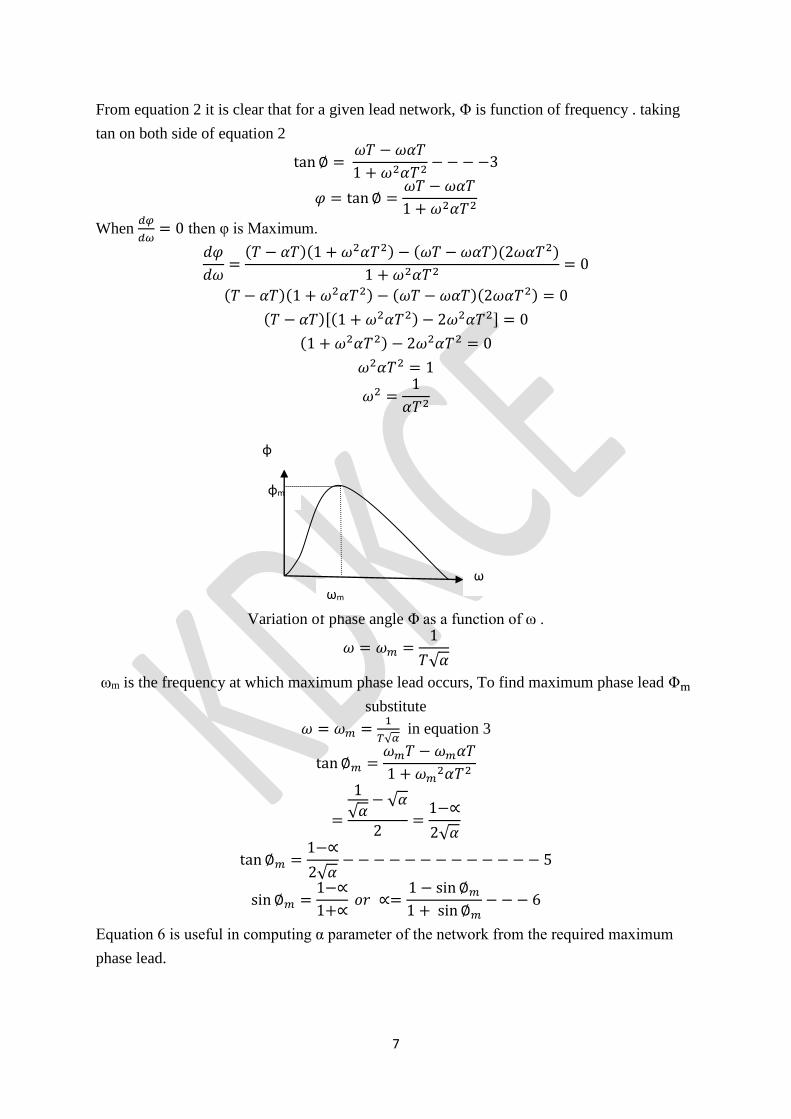
From equation 2 it is clear that for a given lead network, Φ is function of frequency . taking
tan on both side of equation 2
tan ∅ = 𝜔𝑇 − 𝜔𝛼𝑇
1 + 𝜔2𝛼𝑇2− − − −3
𝜑 = tan ∅ =𝜔𝑇 − 𝜔𝛼𝑇
1 + 𝜔2𝛼𝑇2
When 𝑑𝜑
𝑑𝜔= 0 then φ is Maximum.
𝑑𝜑
𝑑𝜔=
(𝑇 − 𝛼𝑇)(1 + 𝜔2𝛼𝑇2) − (𝜔𝑇 − 𝜔𝛼𝑇)(2𝜔𝛼𝑇2)
1 + 𝜔2𝛼𝑇2= 0
(𝑇 − 𝛼𝑇)(1 + 𝜔2𝛼𝑇2) − (𝜔𝑇 − 𝜔𝛼𝑇)(2𝜔𝛼𝑇2) = 0
(𝑇 − 𝛼𝑇)[(1 + 𝜔2𝛼𝑇2) − 2𝜔2𝛼𝑇2] = 0
(1 + 𝜔2𝛼𝑇2) − 2𝜔2𝛼𝑇2 = 0
𝜔2𝛼𝑇2 = 1
𝜔2 =1
𝛼𝑇2
Variation of phase angle Φ as a function of ω .
𝜔 = 𝜔𝑚 =1
𝑇√𝛼
ωm is the frequency at which maximum phase lead occurs, To find maximum phase lead Φm
substitute
𝜔 = 𝜔𝑚 =1
𝑇√𝛼 in equation 3
tan ∅𝑚 =𝜔𝑚𝑇 − 𝜔𝑚𝛼𝑇
1 + 𝜔𝑚2𝛼𝑇2
=
1
√𝛼− √𝛼
2=
1−∝
2√𝛼
tan ∅𝑚 =1−∝
2√𝛼− − − − − − − − − − − − − 5
sin ∅𝑚 =1−∝
1+∝ 𝑜𝑟 ∝=
1 − sin ∅𝑚
1 + sin ∅𝑚− − − 6
Equation 6 is useful in computing α parameter of the network from the required maximum
phase lead.
φm
ωm
ω
φ
8
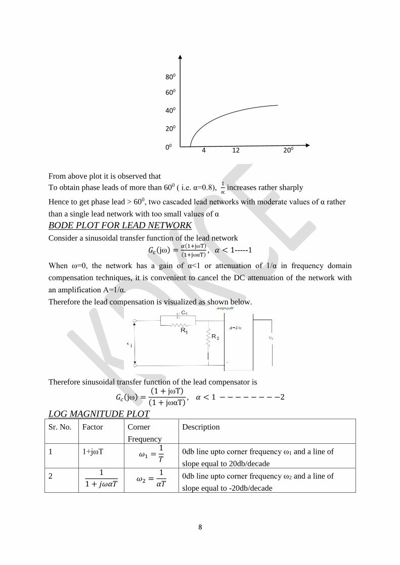
From above plot it is observed that
To obtain phase leads of more than 600 ( i.e. α=0.8), 1
∝ increases rather sharply
Hence to get phase lead > 600, two cascaded lead networks with moderate values of α rather
than a single lead network with too small values of α
BODE PLOT FOR LEAD NETWORK
Consider a sinusoidal transfer function of the lead network
𝐺𝑐(jω) =𝛼(1+jωT)
(1+jωαT), 𝛼 < 1-----1
When ω=0, the network has a gain of α<1 or attenuation of 1/α in frequency domain
compensation techniques, it is convenient to cancel the DC attenuation of the network with
an amplification A=1/α.
Therefore the lead compensation is visualized as shown below.
Therefore sinusoidal transfer function of the lead compensator is
𝐺𝑐(jω) =(1 + jωT)
(1 + jωαT), 𝛼 < 1 − − − − − − − −2
LOG MAGNITUDE PLOT
Sr. No. Factor Corner
Frequency
Description
1 1+jωT 𝜔1 =1
𝑇 0db line upto corner frequency ω1 and a line of
slope equal to 20db/decade
2 1
1 + 𝑗𝜔𝛼𝑇 𝜔2 =
1
𝛼𝑇 0db line upto corner frequency ω2 and a line of
slope equal to -20db/decade
4 200 12
600
400
200
00
800
9
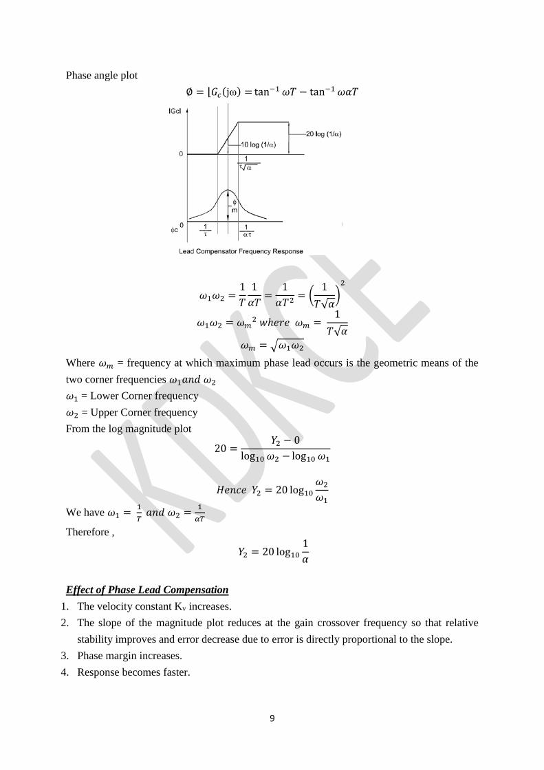
Phase angle plot
∅ = ⌊𝐺𝑐(jω) = tan−1 𝜔𝑇 − tan−1 𝜔𝛼𝑇
𝜔1𝜔2 =1
𝑇
1
𝛼𝑇=
1
𝛼𝑇2= (
1
𝑇√𝛼)
2
𝜔1𝜔2 = 𝜔𝑚2 𝑤ℎ𝑒𝑟𝑒 𝜔𝑚 =
1
𝑇√𝛼
𝜔𝑚 = √𝜔1𝜔2
Where 𝜔𝑚 = frequency at which maximum phase lead occurs is the geometric means of the
two corner frequencies 𝜔1𝑎𝑛𝑑 𝜔2
𝜔1 = Lower Corner frequency
𝜔2 = Upper Corner frequency
From the log magnitude plot
20 =𝑌2 − 0
log10 𝜔2 − log10 𝜔1
𝐻𝑒𝑛𝑐𝑒 𝑌2 = 20 log10
𝜔2
𝜔1
We have 𝜔1 = 1
𝑇 𝑎𝑛𝑑 𝜔2 =
1
𝛼𝑇
Therefore ,
𝑌2 = 20 log10
1
𝛼
Effect of Phase Lead Compensation
1. The velocity constant Kv increases.
2. The slope of the magnitude plot reduces at the gain crossover frequency so that relative
stability improves and error decrease due to error is directly proportional to the slope.
3. Phase margin increases.
4. Response becomes faster.
10
Advantages of Phase Lead Compensation
Let us discuss some of the advantages of the phase lead compensation-
1. Due to the presence of phase lead network the speed of the system increases because it
shifts gain crossover frequency to a higher value.
2. Due to the presence of phase lead compensation maximum overshoot of the system
decreases.
Disadvantages of Phase Lead Compensation
Some of the disadvantages of the phase lead compensation -
1. Steady state error is not improved.
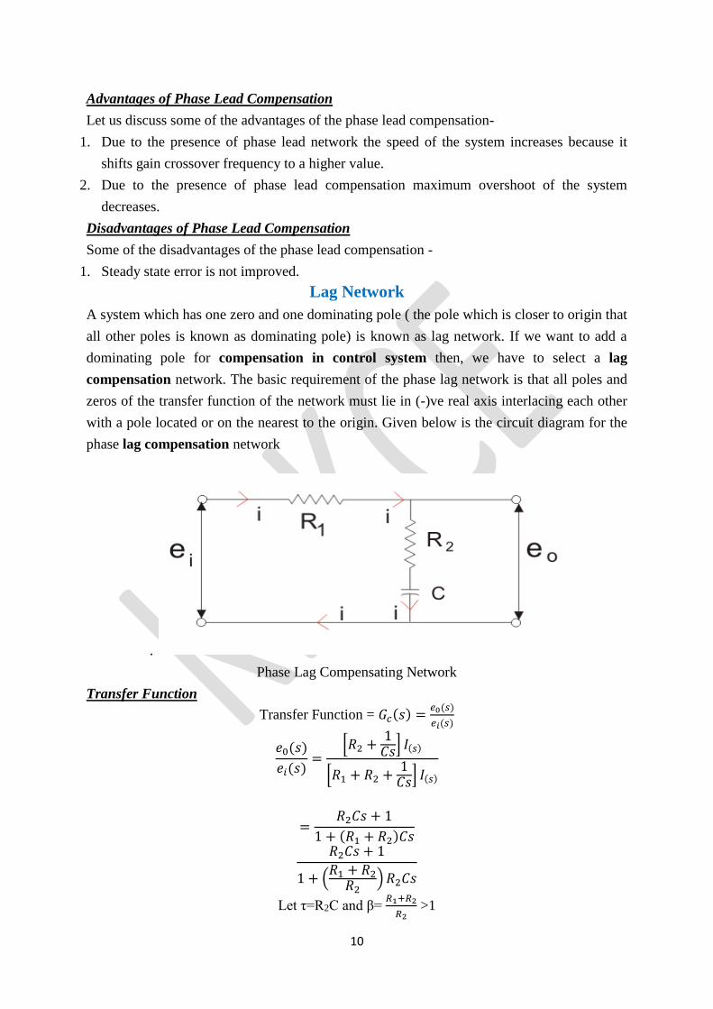
Lag Network
A system which has one zero and one dominating pole ( the pole which is closer to origin that
all other poles is known as dominating pole) is known as lag network. If we want to add a
dominating pole for compensation in control system then, we have to select a lag
compensation network. The basic requirement of the phase lag network is that all poles and
zeros of the transfer function of the network must lie in (-)ve real axis interlacing each other
with a pole located or on the nearest to the origin. Given below is the circuit diagram for the
phase lag compensation network
.
Phase Lag Compensating Network
Transfer Function
Transfer Function = 𝐺𝑐(𝑠) =𝑒0(𝑠)
𝑒𝑖(𝑠)
𝑒0(𝑠)
𝑒𝑖(𝑠)=
[𝑅2 +1
𝐶𝑠] 𝐼(𝑠)
[𝑅1 + 𝑅2 +1
𝐶𝑠] 𝐼(𝑠)
=𝑅2𝐶𝑠 + 1
1 + (𝑅1 + 𝑅2)𝐶𝑠
𝑅2𝐶𝑠 + 1
1 + (𝑅1 + 𝑅2
𝑅2) 𝑅2𝐶𝑠
Let τ=R2C and β= 𝑅1+𝑅2
𝑅2 >1
11
𝐺𝑐(𝑠) =1 + 𝑠𝜏
1 + 𝛽𝑠𝜏− − − − − − − −1
𝐺𝑐(𝑠) =𝑒0(𝑠)
𝑒𝑖(𝑠)=
1
𝛽[
𝑠 +1𝜏
𝑠 +1
𝛽𝜏
] =1
𝛽[𝑠 + 𝑍𝑐
𝑠 + 𝑃𝑐]
Where 𝑍𝑐 =1
𝜏 𝑎𝑛𝑑 𝑃𝑐 =
1
𝜏𝛽
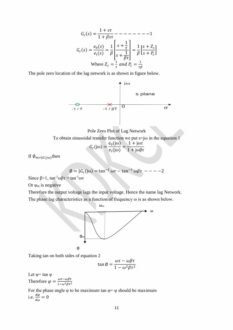
The pole zero location of the lag network is as shown in figure below.
Pole Zero Plot of Lag Network
To obtain sinusoidal transfer function we put s=jω in the equation 1
𝐺𝑐(jω) =𝑒0(jω)
𝑒𝑖(jω)=
1 + jωτ
1 + jωβτ
If ∅𝑚=⌊𝐺(𝑗𝜔)then
∅ = ⌊𝐺𝑐(jω) = tan−1 𝜔𝜏 − tan−1 𝜔𝛽𝜏 − − − −2
Since β>1, tan-1ωβτ > tan-1ωτ
Or φm is negative
Therefore the output voltage lags the input voltage. Hence the name lag Network.
The phase lag characteristics as a function of frequency ω is as shown below.
Taking tan on both sides of equation 2
tan ∅ =𝜔𝜏 − 𝜔𝛽𝜏
1 − 𝜔2𝛽𝜏2
Let ψ= tan φ
Therefore 𝜑 =𝜔𝜏−𝜔𝛽𝜏
1−𝜔2𝛽𝜏2
For the phase angle φ to be maximum tan φ= ψ should be maximum
i.e. 𝑑𝜑
𝑑𝜔= 0
φm
ωm
ω
φ
12
i.e. 𝑑𝜑
𝑑𝜔=
(1+𝜔2𝛽𝜏2)(𝜏−𝛽𝜏)−(𝜔𝜏−𝜔𝛽𝜏)(2𝜔𝛽𝜏2)
(1+𝜔2𝛽𝜏2)= 0
after solving, we get
𝜔 = 𝜔𝑚 =1
𝜏√𝛽
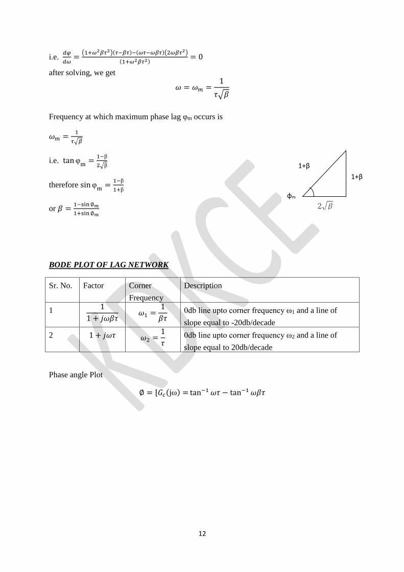
Frequency at which maximum phase lag φm occurs is
𝜔𝑚 =1
𝜏√𝛽
i.e. tan φm
=1−β
2√β
therefore sin φm
=1−β
1+β
or 𝛽 =1−sin ∅𝑚
1+sin ∅𝑚
BODE PLOT OF LAG NETWORK
Sr. No. Factor Corner
Frequency
Description
1 1
1 + 𝑗𝜔𝛽𝜏 𝜔1 =
1
𝛽𝜏 0db line upto corner frequency ω1 and a line of
slope equal to -20db/decade
2 1 + 𝑗𝜔𝜏 𝜔2 =1
𝜏 0db line upto corner frequency ω2 and a line of
slope equal to 20db/decade
Phase angle Plot
∅ = ⌊𝐺𝑐(jω) = tan−1 𝜔𝜏 − tan−1 𝜔𝛽𝜏
φm
1+β
2√𝛽
1+β
13
𝜔1𝜔2 =1
𝛽𝜏2=
1
(𝜏√𝛽)2 = 𝜔𝑚
2
𝜔𝑚 = √𝜔1𝜔2
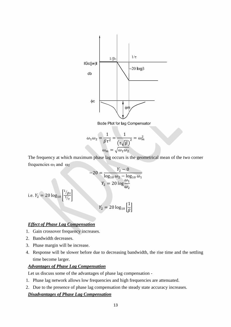
The frequency at which maximum phase lag occurs is the geometrical mean of the two corner
frequencies ω1 and ω2
−20 =𝑌2 − 0
log10 𝜔2 − log10 𝜔1
𝑌2 = 20 log𝜔1
𝜔2
i.e. 𝑌2 = 20 log10 [1
𝛽𝜏⁄
1𝜏⁄
]
𝑌2 = 20 log10 [1
𝛽]
Effect of Phase Lag Compensation
1. Gain crossover frequency increases.
2. Bandwidth decreases.
3. Phase margin will be increase.
4. Response will be slower before due to decreasing bandwidth, the rise time and the settling
time become larger.
Advantages of Phase Lag Compensation
Let us discuss some of the advantages of phase lag compensation -
1. Phase lag network allows low frequencies and high frequencies are attenuated.
2. Due to the presence of phase lag compensation the steady state accuracy increases.
Disadvantages of Phase Lag Compensation
14
Some of the disadvantages of the phase lag compensation -
1. Due to the presence of phase lag compensation the speed of the system decreases.
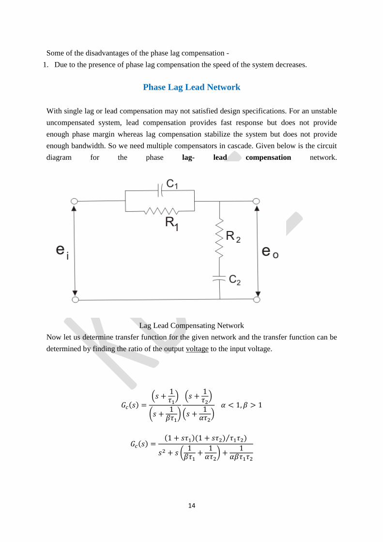
Phase Lag Lead Network
With single lag or lead compensation may not satisfied design specifications. For an unstable
uncompensated system, lead compensation provides fast response but does not provide
enough phase margin whereas lag compensation stabilize the system but does not provide
enough bandwidth. So we need multiple compensators in cascade. Given below is the circuit
diagram for the phase lag- lead compensation network.
Lag Lead Compensating Network
Now let us determine transfer function for the given network and the transfer function can be
determined by finding the ratio of the output voltage to the input voltage.
𝐺𝑐(𝑠) =(𝑠 +
1𝜏1
)
(𝑠 +1
𝛽𝜏1)
(𝑠 +1𝜏2
)
(𝑠 +1
𝛼𝜏2)
𝛼 < 1, 𝛽 > 1
𝐺𝑐(𝑠) =(1 + 𝑠𝜏1)(1 + 𝑠𝜏2) 𝜏1𝜏2⁄ )
𝑠2 + 𝑠 (1
𝛽𝜏1+
1𝛼𝜏2
) +1
𝛼𝛽𝜏1𝜏2
15
=(1 + 𝑠𝜏1)(1 + 𝑠𝜏2)
𝜏1𝜏2𝑠2 + 𝑠 (𝜏1
𝛼 +𝜏2
𝛽) +
1𝛼𝛽
− − − − − − − − − − − −1
We have,
𝑒0(𝑠) = [𝑅2 +1
𝐶2𝑠] 𝐼(𝑠)
𝑒𝑖(𝑠) = [𝑅1
1𝐶1𝑠
𝑅1 +1
𝐶1𝑠
+ 𝑅2 +1
𝐶2𝑠] 𝐼(𝑠)
𝑒𝑖(𝑠)
𝛽𝑒𝑜(𝑠)=
[𝑅1
𝑅1𝐶1𝑠 + 1 + 𝑅2 +1
𝐶2𝑠]
[𝑅2 +1
𝐶2𝑠]
𝑒𝑖(𝑠)
𝑒𝑜(𝑠)=
𝑅1𝐶1𝑠 + (𝑅2𝐶2𝑠 + 1)(𝑅1𝐶1𝑠 + 1)
(𝑅1𝐶1𝑠 + 1)(𝑅2𝐶2𝑠 + 1)
𝐺𝑐(𝑠) =(𝑅1𝐶1𝑠 + 1)(𝑅2𝐶2𝑠 + 1)
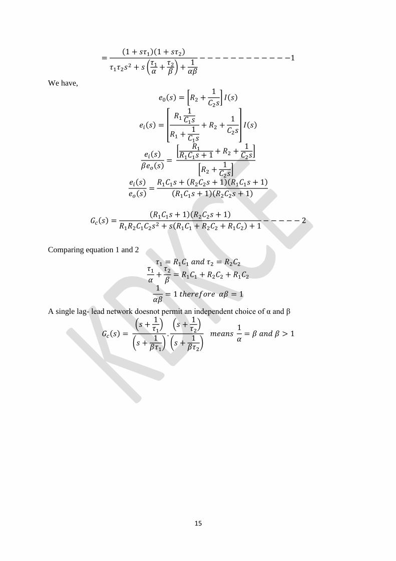
𝑅1𝑅2𝐶1𝐶2𝑠2 + 𝑠(𝑅1𝐶1 + 𝑅2𝐶2 + 𝑅1𝐶2) + 1− − − − − 2
Comparing equation 1 and 2
𝜏1 = 𝑅1𝐶1 𝑎𝑛𝑑 𝜏2 = 𝑅2𝐶2 𝜏1
𝛼+
𝜏2
𝛽= 𝑅1𝐶1 + 𝑅2𝐶2 + 𝑅1𝐶2
1
𝛼𝛽= 1 𝑡ℎ𝑒𝑟𝑒𝑓𝑜𝑟𝑒 𝛼𝛽 = 1
A single lag- lead network doesnot permit an independent choice of α and β
𝐺𝑐(𝑠) = (𝑠 +
1𝜏1
)
(𝑠 +1
𝛽𝜏1)
.(𝑠 +
1𝜏2
)
(𝑠 +1
𝛽𝜏2)
𝑚𝑒𝑎𝑛𝑠 1
𝛼= 𝛽 𝑎𝑛𝑑 𝛽 > 1
16
Pole Zero Plot Lag Lead Network
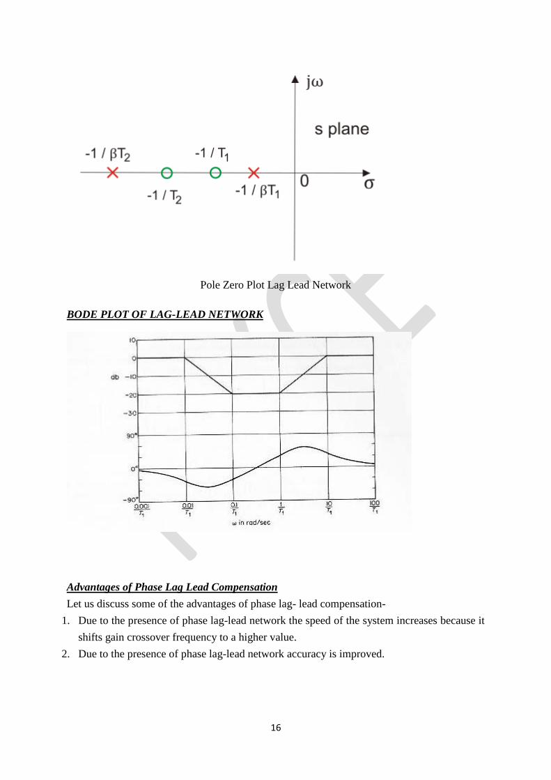
BODE PLOT OF LAG-LEAD NETWORK
Advantages of Phase Lag Lead Compensation
Let us discuss some of the advantages of phase lag- lead compensation-
1. Due to the presence of phase lag-lead network the speed of the system increases because it
shifts gain crossover frequency to a higher value.
2. Due to the presence of phase lag-lead network accuracy is improved.
17
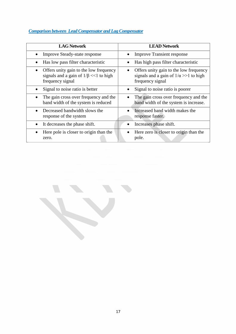
Comparison between Lead Compensator and Lag Compensator
LAG Network LEAD Network
• Improve Steady-state response • Improve Transient response
• Has low pass filter characteristic • Has high pass filter characteristic
• Offers unity gain to the low frequency
signals and a gain of 1/β <<1 to high
frequency signal
• Offers unity gain to the low frequency
signals and a gain of 1/α >>1 to high
frequency signal
• Signal to noise ratio is better • Signal to noise ratio is poorer
• The gain cross over frequency and the
band width of the system is reduced
• The gain cross over frequency and the
band width of the system is increase.
• Decreased bandwidth slows the
response of the system
• Increased band width makes the
response faster.
• It decreases the phase shift. • Increases phase shift.
• Here pole is closer to origin than the
zero.
• Here zero is closer to origin than the
pole.