Embed Size (px)
Citation preview

Control System for Glucose Detector System
by
David Smith
Senior Project
ELECTRICAL ENGINEERING DEPARTMENT
California Polytechnic State University
San Luis Obispo
2012

2 | P a g e
Table of Contents Title Page ...................................................................................................................................................... 1
Table of Contents ......................................................................................................................................... 2
List of Tables and Figures ............................................................................................................................. 3
Acknowledgements ..................................................................................................................................... 4
Abstract ........................................................................................................................................................ 4
Introduction .................................................................................................................................................. 5
Background ................................................................................................................................................... 6
Requirements ............................................................................................................................................... 7
Design ........................................................................................................................................................... 8
Test Plans .................................................................................................................................................... 12
Development .............................................................................................................................................. 13
RS Flip Flop Design .............................................................................................................................. 13
Comparator Design using Differential Pairs with Active Loading ....................................................... 15
Ten Minute Timer Design.................................................................................................................... 17
One Shot Design .................................................................................................................................. 20
The Entire Circuit ................................................................................................................................ 21
Conclusion .................................................................................................................................................. 26
Bibliography................................................................................................................................................ 27
Appendix A: Senior Project Analysis .......................................................................................................... 28

3 | P a g e
List of Tables of Figures Table
1. Complete Circuit Performance with Varying Supply Voltages ................................................................. 1
Figures
1. Block Diagram of Finished System ........................................................................................................... 8
2. Schematic of 555 Timer ........................................................................................................................... 9
3. RS Flip Flop Design .................................................................................................................................. 9
4. NOR Gate Schematic ............................................................................................................................. 10
5. Differential Pair Schematic .................................................................................................................... 11
6. RS Flip Flop Schematic ............................................................................................................................ 13
7. RS Flip Flop Waveform ........................................................................................................................... 14
8. Differential Pair Schematic ..................................................................................................................... 15
9. Differential Pair Waveform ................................................................................................................... 16
10. Setup for using a 555 Timer as a Square Wave Generator ................................................................. 17
11. 10-Minute Timer Schematic ................................................................................................................. 18
12. 10-Minute Timer Output Waveform ................................................................................................... 19
13. Setup for using 555 Timer as a Monostable ....................................................................................... 20
14. Entire Circuit Schematic ...................................................................................................................... 22
15. Output Pulses from Completed Circuit ............................................................................................... 23
16. Zoomed in Output Waveform ............................................................................................................. 24
17. Current Coming from the Voltage Source ........................................................................................... 25

4 | P a g e
Acknowledgements:
Tina Smilkstein
Abstract: In this paper I design and test on a prove of concept level a control/timing circuit for a blood glucose
detector built in a previous senior project. The specifications of the design given are to properly power
the detector with a low power source. The design is completed on a transistor level basis using Cadence
Virtuoso Software. The system is design from the ground up; designing, building, and testing smaller
circuits first then combined into increasingly larger circuits till the completed circuit is finished. The
design used to based off of the 555 Timer and uses differential pairs, CMOS designed NOR gates, flip
flops. The control system is also modified to be low power and to be able to use low voltage power
source.

5 | P a g e
I: Introduction Diabetes is a wide-spread problem around the world and especially in America. The American Diabetes
Association states that in 2011 25.8 million people in America alone have some form of diabetes [1].
Diabetes is a metabolic disorder where the body’s cells are inefficient at using the sugar in the blood
stream for energy. This leads to high amounts of blood sugar which can be measure. This is believed to
be caused by the rise of obesity in America as well as other causes. There are many ways to combat this
problem of diabetes but for those who already have it or are born with it the most common way to live
with and control it are insulin injections. Blood sugar levels are needed to determine when and how
much insulin is needed to bring the blood sugar levels back to a normal level. Most blood glucose (a
primary type of sugar in humans) detectors require the user to bleed on the detector, which usually
involves pricking a finger. The system designed by (who did this) uses an oscillator, electrode, detector
and other supporting circuitry to measure a phase shift of a signal through the arm to determine blood
sugar levels. The main advantage of this system is that it is non-intrusive, not requiring any pricking or
bleeding. The problem set out to solve for this paper is a way to make a control system for this larger
system that can run on so little power that it can run off of power scavenged from the users own breath.
This is to be a completely self-sustaining system so the user would not have to worry about anything and
can have information about their blood glucose levels every ten minutes.

6 | P a g e
II: Background Last year another senior project was created to use a phase shift detector as a low power way to
measure blood glucose levels in a person. The project was a success but required power from a wall or
other external source to operate. This project was to create a low power control system that could
operate on power extracted from the person’s own breathing. The point of this is that anyone, even a
quadriplegic could generate the power required to operate the device so that he/she would never have
to worry about batteries or charging it. Cadence is used to design a series of timer circuits to power on
the glucose detector for 1 second once every ten minutes. The basic design of the system uses the 555
timer design invented by Hans R. Camenzind in 1970.
The Cadence files used are for AMI 06 and AMI 07 NMOS and PMOS transistors. These model files are
chosen as being reasonably close to the type of transistor that will be manufactured in the completed
circuit.

7 | P a g e
III: Requirements
The final system shall be able to:
• Run off of a rail voltage of between 1.5V and 5V
• Use as little power as possible
• Turn on the glucose detector by providing the correct power and voltage once every ten (10)
minutes
• Provide power to all supporting systems at the correct time intervals to minimize power usage
and allow the device to output correctly
• The outputs of the circuit are a one second pulse, and a two second pulse
8 | P a g e
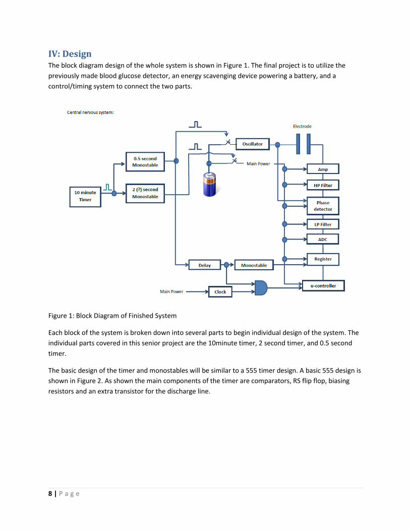
IV: Design The block diagram design of the whole system is shown in Figure 1. The final project is to utilize the
previously made blood glucose detector, an energy scavenging device powering a battery, and a
control/timing system to connect the two parts.
Figure 1: Block Diagram of Finished System
Each block of the system is broken down into several parts to begin individual design of the system. The
individual parts covered in this senior project are the 10minute timer, 2 second timer, and 0.5 second
timer.
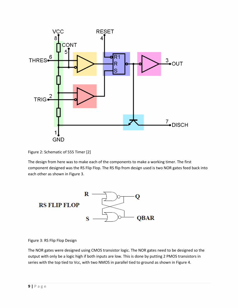
The basic design of the timer and monostables will be similar to a 555 timer design. A basic 555 design is
shown in Figure 2. As shown the main components of the timer are comparators, RS flip flop, biasing
resistors and an extra transistor for the discharge line.
9 | P a g e
Figure 2: Schematic of 555 Timer [2]
The design from here was to make each of the components to make a working timer. The first
component designed was the RS Flip Flop. The RS flip from design used is two NOR gates feed back into
each other as shown in Figure 3.
Figure 3: RS Flip Flop Design
The NOR gates were designed using CMOS transistor logic. The NOR gates need to be designed so the
output with only be a logic high if both inputs are low. This is done by putting 2 PMOS transistors in
series with the top tied to Vcc, with two NMOS in parallel tied to ground as shown in Figure 4.

10 | P a g e
Figure 4: NOR Gate Schematic from http://people.rit.edu/lffeee/cmosvlsi.pdf
The other major component of the timer is two comparators. The design used for the comparators are
differential pairs with biasing circuitry. A typical CMOS differential pair is shown in Figure 5.

11 | P a g e
Figure 5: Differential Pair Schematic from
http://webpages.eng.wayne.edu/cadence/ECE7570/doc/comparator.pdf
This exact design was not used in final design.
12 | P a g e
V: Test Plans Initial testing of the system is done in Cadence to individual components using a proof of concept
method. This method is to generate a schematic of the individual parts and put in test signals to verify
that the system outputs correctly. Each component will be tested individually to show proper
performance. Once every system is shown to work properly the whole circuit will be assembled in
Cadence layout and will be simulated with test parameters.

13 | P a g e
VI: Development
The system was developed one component at a time in Cadence as a schematic on the transistor level.
RS Flip Flop Design
Figure6: RS Flip Flop Schematic
The RS Flip Flop schematic was laid out in Cadence. The Vcc was set to 5 volts and input square waves
oscillating to show that the output would set and reset with the appropriate signals. The results are
shown in Figure 7.

14 | P a g e
Figure 7: RS Flip Flop Waveform
The thicker dashed line is the output Q of the circuit. The light blue line is reset, and the black line is set.
The input waves are set to 30 ms period with high times are 10ms and are offset from each other to
show that the signal stays at its current value when both signals are low. As shown, the output Q stays
at its current level with R and S are low and sets and resets properly.

15 | P a g e
Comparator Design using Differential Pairs with Active Loading
Figure 8: Differential Pair Schematic
Figure 8 shows input sign waves are used to show correct function of differential pair. The differential
pair uses a current mirror to provide a steady current through the differential pair to create the
necessary drive turn the transistors on and off to allow for maximum voltage swing in the output. Again
the rail voltage is 5 Vdc. The input sine waves were set to a frequency of 100 Hz just to show prove of
concept in the design and not to test bandwidth of the system.
The biasing resistor value was chosen to provide a 10µA current to the differential pair. In order to
calculate R, Vdsat was first calculated.
VGsat = VGS – Vt ´
K´=µn*cox= µn*
For silicon K´=459.43 ... =113.9µA/V
For our transistor with w= 4µm and l=1.6µm
16 | P a g e
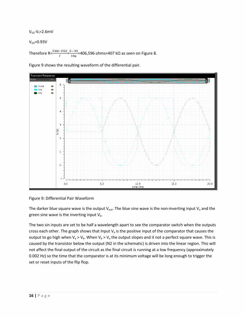
VGS-Vt=2.6mV
VGS=0.93V
Therefore R= ! "# =
!.$ =406,596 ohms≈407 kΩ as seen on Figure 8.
Figure 9 shows the resulting waveform of the differential pair.
Figure 9: Differential Pair Waveform
The darker blue square wave is the output Vout. The blue sine wave is the non-inverting input Va and the
green sine wave is the inverting input Vb.
The two sin inputs are set to be half a wavelength apart to see the comparator switch when the outputs
cross each other. The graph shows that Input Va is the positive input of the comparator that causes the
output to go high when Va > Vb. When Vb > Va the output slopes and it not a perfect square wave. This is
caused by the transistor below the output (N2 in the schematic) is driven into the linear region. This will
not affect the final output of the circuit as the final circuit is running at a low frequency (approximately
0.002 Hz) so the time that the comparator is at its minimum voltage will be long enough to trigger the
set or reset inputs of the flip flop.

17 | P a g e
10-Minute Timer
A 10-minute timer is created by using 2 resistor and a capacitor external to the timer circuit itself as
shown in Figure 10.
Figure 10: Setup for using a 555 Timer as a Square Wave Generator from
http://www.kpsec.freeuk.com/555timer.htm
To create a 10-minute timer, the period needs to be set to 600 seconds. By combining Figures 2 and 10,
one can determine how the timer works. When the voltage across the capacitor is at 1/3 Vs it will
charge, attempting to reach Vs. In this state the output, Q is high, so the discharge transistor is off
causing the capacitor C1 to charge from Vs through R1 and R2. Once the voltage across the capacitor
reaches 2/3 Vs the top comparator will reset the flip flop causing the output to go low and turns on the
discharge transistor. At this point the capacitor will discharge through R2. To find the period of the
output square wave use these equations
T = 0.693*(R1+2*R2)*C
Where T = total period of the waveform
The values used are
R1 = 500 kΩ
R2 = 2.6 MΩ
C = 175 µF
Figure 11 shows the complete 10-minute timer
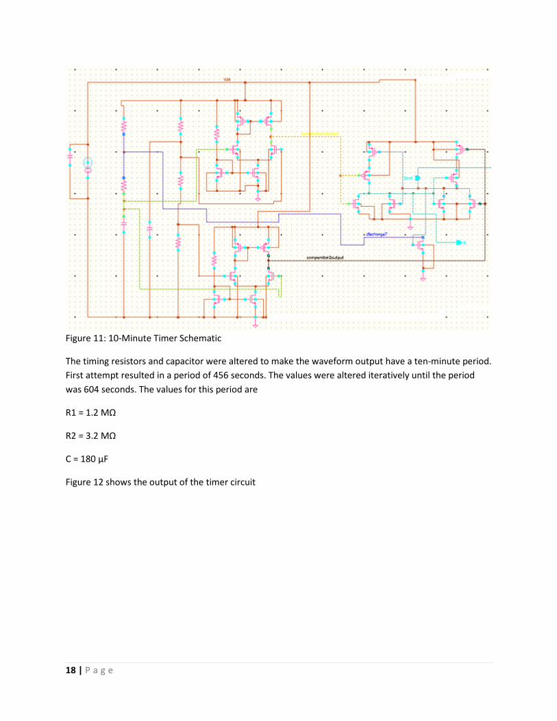
18 | P a g e
Figure 11: 10-Minute Timer Schematic
The timing resistors and capacitor were altered to make the waveform output have a ten-minute period.
First attempt resulted in a period of 456 seconds. The values were altered iteratively until the period
was 604 seconds. The values for this period are
R1 = 1.2 MΩ
R2 = 3.2 MΩ
C = 180 µF
Figure 12 shows the output of the timer circuit

19 | P a g e
Figure 12: 10-Minute Timer Output Waveform
For this circuit the only inputs are the power and ground rails. The period and duty cycle determined by
capacitive charging time constant affected by the resistor and capacitor values. The output was taken to
be Qnot because it had a cleaner output signal. As the one shots need to be triggered once every ten
minutes it does not matter whether Q or Qnot is because they both have the same period.

20 | P a g e
One Shot Design
The monostable circuits will also comprise of the timer circuit but configured to create a monostable
circuit, shown in Figure 13.
Figure 13: Setup for using 555 Timer as a Monostable
The trigger of this setup is the output of the 10-minute timer. The output is the control signal for the
glucose detection system. The system works by starting in with Q low. In this state the discharge
transistor is on so there is no voltage across the capacitor. When it is triggered the comparator sets the
flip flop causing the discharge transistor to turn off so the capacitor charges through R1. The capacitor
will charge until it reaches 2/3 Vs than the other comparator will reset the flip flop causing the discharge
transistor to turn on. The capacitor will then discharge through the discharge transistor and will return
to the beginning state. The output is only high during the time it takes to charge the capacitor to 2/3 Vs.
The two desired times are 0.5 and 2 seconds. Use the equation below to find the length of time T that
the monostable will go high
T = 1.1 * R * C
For half second
R = 45.45 kΩ
C = 12 µF
For two second
R = 181.8 kΩ
C = 12 µF

21 | P a g e
The Complete Circuit and Test Results
All the parts are interconnected with the output of the 10-minute timer used to trigger the two
monostables one shots. The outputs of the circuit are the outputs of the one shots.

22 | P a g e
Figure 14: Entire Circuit Schematic

23 | P a g e
The resulting output waveforms are this are shown in Figures 15 and 16.
Figure 15: Output Pulses from Completed Circuit
Figure 15 shows that the outputs from the two monostables are short pulses that occur once every 600
seconds, or 10 minutes. The first pulse takes longer to happen because the capacitor is charging from
ground instead of 1/3 Vcc. This is advantageous for the final system as the battery needs to be charged
by breathing when first used and needs the extra time for initial charge.

24 | P a g e
Figure 16: Zoomed in Output Waveform
Figure 16 shows the duration of the pulses from the outputs. The pink line is approximately 0.5 seconds
wide and goes from 0 to 5 V. The green varies as it decays; it reaches 2.5 V, half of the peak voltage at 2
seconds from the time it turns on.
An important factor for the project was power usage by the control system. Figure 17 Shows the current
coming from the 5 V source to show power used since P = I*V.

25 | P a g e
Figure 17: Current Coming from the Voltage Source
The orange line is current coming from the voltage source Vdd and uses the current scale on the right
side of the graphic.
The peak current coming from the source is 465 uA meaning the greatest instantaneous power draw is
2.325 mW. The lowest current is 100uA corresponding to 0.5 mW. The average current draw is
approximately 180uA, meaning the average power usage is .9mW.
Vcc was then altered to see if the circuit would still work with lower voltages. Table 1 shows how
different voltages compare:
Voltage (V) Power Max
(mW)
Power Min
(mW)
Period (s) Length of Pulse
(short) (s)
Length of Pulse
(long) (s)
6 4.152 0.810 496 0.568 1.605
5 2.325 0.500 603 0.500 2.00
4 1.292 0.338 743 0.500 2.383
3 0.558 0.153 800 0.507 2.253
Table 1: Complete Circuit Performance with Varying Supply Voltages
For voltages 2.5 and below monostables would not have a repeating output. The circuit would pulse
once at 700 seconds and then remain at 0 V. This shows that the circuit is dependent on a constant
voltage supply to function properly.
26 | P a g e
VII: Conclusion The circuit behaved in the end as predicted with a few exceptions. The timer circuits were adjusted to
create the desired period and pulse lengths of the outputs. The initial design of the 10 minute timer
resulted in a period of only 460 seconds which is 7 minutes and 40 seconds. This could have been from
extra capacitance from the transistors that is not accounted for in the timer equations. The half and two
second pulses worked correctly from the start with accuracy greater than that measured by the Cadence
simulator system for the half second pulse. The two second pulse was not a clean square wave as
desired. It took 0.6 seconds to go from 5 to 0 volts. This phenomenon could be caused by the
capacitance of the transistors or by one or more transistors being biased in the linear region.
This circuit could be continued in Cadence and be made into a layout design using Virtuoso Layout XL.
That program can take a Cadence schematic file and convert the pieces into a silicon layout design. This
was not done in this project due to technical difficulties with the software and licensing issues. After
successfully completing a layout the circuit file can be sent to a manufacturer and produced in silicon
and implemented in the larger system.

27 | P a g e
VIII: Bibliography [1] American Diabetes Association, “Diabetes Statistics”, Jan. 26, 2011, [Online] Available:
http://www.diabetes.org/diabetes-basics/diabetes-statistics/ [Accessed June 1, 2012]
[2] Unknown Author “LM555 and LM556 Timer Circuits”, Apr. 22, 2012, [Online] Available:
http://home.cogeco.ca/~rpaisley4/LM555.html, [Accessed June 1, 2012]
[3] Unknown Author “CMOS Comparator”, Unknown date, [Online] Available:
http://webpages.eng.wayne.edu/cadence/ECE7570/doc/comparator.pdf, [Accessed June 1,
2012]
[4]James Hewes, 555 and 556 Timer Circuits, 2011, [Online] Available:
http://www.kpsec.freeuk.com/555timer.htm, [Accessed May 20, 2012]
[5] John Wakerly, Digital Design, Principle and Practices. 4th ed. Pearson Education, Inc. 2006
28 | P a g e
IX: Appendices
A: Senior Project Analysis
Project Title: Control System for Blood Glucose Detector
David Smith
Tina Smilkstein: Initials:
Summary of Functional Requirements:
The system is to run off of a low power source and provide power to a blood glucose detector and
supporting hardware once every 10 minutes. The lengths of time the power is need for the oscillator is
0.5 seconds and for the supporting hardware is 2 seconds.
Primary Constraints:
A main limiting factor for designing was the lack of access to the software used to design, in this case
Cadence. The limiting factor for the design was the low amount of power available to the project as the
desired source is energy scavenged from breathing.
Economic:
The project consists of the time and research of the design to originally produce. The financial capital of
an investor is needed to have a manufacturer produce the chip and other hardware. The price of the
part would be initially paid for by the investor for the company. Once commercially sold, customers and
their health insurance would be providing the funds for the materials and construction costs. The
product would be built by several contractors. The parts needed to be sent out are the chip designed in
this project and the battery or large capacitor used to hold charge. The breathing apparatus can be built
by students on campus as part of the assembly process.
Environmental:
Since the system is self-sustaining there is almost no environmental impact. The environmental impact
comes from the manufacturing of the device. It requires silicon and a manufacturing plant capable of
creating transistors on silicon chips and the chemicals that process requires.
Manufacturability:
Transistor technology is widespread with several large manufacturers. The primary constraint to
manufacturing is the wait time for chip production. The production and size of energy scavenging
harness is manufacturing difficulty not covered in this paper.
Sustainability:

29 | P a g e
The system once assembled would be low maintenance. It would power itself and be made reliably. The
main problems that could occur are mechanical failure of the power scavenging device or the
interconnections of the system.
The system can be upgraded by improving the design or layout of the control system to be less lossy and
to run on smaller amounts of power. The energy scavenging process could also be upgraded by using
different materials or patterns in order to generate a greater current for the power source.
Ethical:
The design needs to be tested extensively to prove that the system as a whole works correctly and
provides an accurate measure of blood glucose levels. Users of the system will trust that the system
works properly and that the reading given them is accurate. Therefore, extensive testing and comparing
this system’s readings against proven systems for measuring those levels must be done before mass
production and sales.
Health and Safety:
For use of the product, one major safety concern is the accuracy of the reading of the device. Proper
readings are needed to decide on the level of insulin needed to lower blood sugar levels. Also safety
while using the energy scavenging is a concern. Breathing apparatus could be too tight or prevent
customer from being able to receive help during a medical emergency.
Social and Political:
This project could help those with diabetes from having to stab themselves on a regular basis to get a
blood glucose reading. It is a non-invasive and painless way to get a blood glucose level that will make
living with diabetes more bearable and far less painful.
Developmental:
I learned through this project how to use Cadence Software to design and develop transistor based
circuits. This is incredibly useful as transistors are the primary circuit device in both analog and digital
circuitry. I also learned the process for completing a layout design in silicon, which can be used for
designing my own integrated circuits in a format that can be sent to a manufacturer to be quickly and
inexpensively produced.