Embed Size (px)
Citation preview
Control of Triboelectrification by Engineering Surface Dipole andSurface Electronic StateKyung-Eun Byun,† Yeonchoo Cho,† Minsu Seol,† Seongsu Kim,‡ Sang-Woo Kim,*,‡ Hyeon-Jin Shin,*,†
Seongjun Park,*,† and Sungwoo Hwang†
†Samsung Advanced Institute of Technology, Suwon 443-803, Republic of Korea‡School of Advanced Materials Science and Engineering, Sungkyunkwan University (SKKU), Suwon 440−746, Republic of Korea
*S Supporting Information
ABSTRACT: Although triboelectrification is a well-knownphenomenon, fundamental understanding of its principle on amaterial surface has not been studied systematically. Here, wedemonstrated that the surface potential, especially the surfacedipoles and surface electronic states, governed the tribo-electrification by controlling the surface with various electron-donating and -withdrawing functional groups. The functionalgroups critically affected the surface dipoles and surfaceelectronic states followed by controlling the amount of andeven the polarity of triboelectric charges. As a result, only onemonolayer with a thickness of less than 1 nm significantlychanged the conventional triboelectric series. First-principles simulations confirmed the atomistic origins of triboelectric chargesand helped elucidate the triboelectrification mechanism. The simulation also revealed for the first time where charges are retainedafter triboelectrification. This study provides new insights to understand triboelectrification.
KEYWORDS: triboelectrification, self-assembled monolayer, electron-donating group, electron-withdrawing group,Kelvin force microscopy
■ INTRODUCTION
Triboelectrification, which is defined as the separation ofcharges by the contact of two materials, has been considered asan interesting phenomenon since the time of ancient Greece.1
Triboelectric charges generated by triboelectrification are usedin diverse applications, including for increasing the selectiveadhesion of the toner particles in printers,2 separating mineralsand coals in electrostatic separators based on the chargepolarity,3 and coating whole objects with charged paintdroplets.4 In particular, a triboelectric nanogenerator(TENG), a device that can convert mechanical energy intoelectrical energy by exploiting the coupling between tribo-electrification and electrostatic induction, has recently beendrawing attentions as a key solution for energy harvesting fromthe waste energy in the environment. Thanks to recent efforts,the output power of the TENG has increased dramatically.Further, it has been demonstrated that the TENG is capable ofpowering touch pad sensors,5 mobile electronics,6 and self-charged vehicle entry systems.7 These efforts include thephysical modification of the relevant surface to increase thefrictional movement as well as the actual contact area byforming pyramid-like patterns,6 fabricating vertically alignednanowires on the surface8 or nanoparticles-coated surface.9
Fine-tuning the device structure by forming an arch for effectivecharge separation,6 multilayers to increase the contact area,10 ora grating to improve the energy conversion efficiency11 has also
resulted in improvements in the output power. However, thefundamental understanding of triboelectrification in a material’spoint of view has not been pursued systematically.One of the main mechanisms to explain triboelectrification is
that the amount of charges exchanged is proportional to thesurface potential (effective work function) difference of the twomaterials being contacted together.12,13 The surface potential ofa material is the overall consequence of the following: bulkelectronic structures, surface dipoles, and surface electronicstates.14,15 While bulk electronic structures are determined bythe given material components and its atomic structures, thesurface dipoles and surface electronic structures can be affectedby various uncontrollable surface conditions, such as surfacereconstructions, adsorbates in air, and surface defects.15 Thus,many contradictory and ambiguous results are observed duringthe triboelectrification measurements.16,17 Recently, severalresearchers have reported the surface potential altered by thesurface functional group affects triboelectrification. Theseresults have focused on the enhancement of triboelectriccharges and explanations have remained at a phenomenologicallevel.18−20 The fundamental understanding regarding a relation-
Received: March 6, 2016Accepted: June 24, 2016Published: June 24, 2016
Research Article
www.acsami.org
© 2016 American Chemical Society 18519 DOI: 10.1021/acsami.6b02802ACS Appl. Mater. Interfaces 2016, 8, 18519−18525
ship between triboelectrification and surface potential ofmaterials was insufficient.In this work, we report effects of the surface potential on
triboelectrification by systematically controlling surface dipolesand surface electronic states through the surface modificationwith various electron-donating and -withdrawing functionalgroups. We characterized the surface potential of self-assembledmonolayer (SAM) modified SiO2 surfaces
21 with Kelvin probeforce microscopy (KPFM)22 to confirm the relationshipbetween the surface potential and triboelectric charges. TheSiO2 with an electron-donating layer such as an NH2 grouptends to donate electrons to the counter metal surface, whilethe SiO2 with an electron-withdrawing layer such as a CF3group, tends to accept electrons from the counter surface.Consequently, SAM altered the conventional triboelectric seriesof original substrates according to the functional group of SAM.We also calculated the surface dipole and surface electronicstates of the SAM-modified materials using first-principlessimulations to understand the atomistic origins of triboelectriccharges and to elucidate the triboelectrification mechanism.This study provides a better understanding of the tribo-
electrification: the surface dipole and surface electronic statesare the critical factors that control the amount of and evenconvert the polarity of triboelectric charges.
■ RESULTS AND DISCUSSION
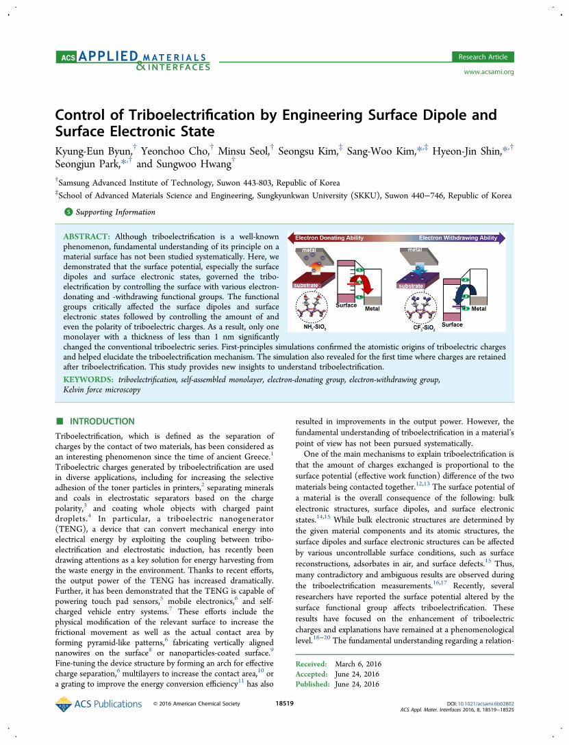
Figure 1 shows a schematic diagram depicting the tribo-electrification of various surface-modified materials. Theuniform and well-ordered SAM in nanoscale effectivelycontrolled surface defects and reduced the adsorption ofadditional adsorbates in air.23 In this way, the effect of surfacepotential on triboelectrification can be monitored without anyartifacts. The functional groups in the SAM, which includedgroups such as −NH2, −SH, −CH3, and −CF3, determinedwhether the surface were electron-donating or electron-withdrawing.24 The lone pair of the NH2 and the SH functionalgroups tends to donate electrons (Figure 1a,i), while the CF3group accepts electrons from an adjacent system, in one case,metal, owing to the presence of the highly electronegative atomF (Figure 1a,iv).25 A weakly electron-donating or a neutralfunctional group such as SH or CH3 donates fewer electrons tothe metal (Figure 1a,ii,iii). Surface modification by SAMs on
Figure 1. Triboelectrification on the SAM-modified substrates with electron-donating and electron-withdrawing groups. (a) Schematic diagram ofthe triboelectrification on (i) a strongly electron-donating layer (−NH2), (ii) a moderate electron-donating layer (−SH), (iii) a neutral layer(−CH3), and (iv) an electron-withdrawing layer (−CF3). The chemical structures of the respective molecules are shown in the dotted circles. (b)CPD images of (i) as-received SiO2 and the (ii) NH2-, (iii) SH-, (iv) CH3-, and (v) CF3-modified SiO2. (c) CPD of each substrate. The empty andfilled symbols represent the CPD before and after contact, respectively. (d) Triboelectric potentials of the various surfaces as a function of the CPDbefore contact.
ACS Applied Materials & Interfaces Research Article
DOI: 10.1021/acsami.6b02802ACS Appl. Mater. Interfaces 2016, 8, 18519−18525
18520
the materials could increase or decrease triboelectric chargesgenerated on surfaces.To verify our hypothesis on the triboelectricity affected by
the surface modification, we employed the KPFM mode inatomic force microscopy (AFM) measurements.12,26 TheKPFM mode allowed the surface potential of the substrate tobe visualized, on the basis of the contact potential difference(CPD) between the probe and the substrate.22 The surfacepotential of the substrate, ϕsubstrate, is defined as
ϕ ϕ= − eVsubstrate probe CPD (1)
where ϕprobe is the work function of the probe, VCPD is themeasured CPD, and e is the electronic charge. After thesubstrate has been contacted, the surface potential should bechanged owing to the triboelectric charges generated. Thetriboelectric potential can be defined by the difference in thesurface potential before and after contact. Figure 1b shows theCPD images of various SAM-modified substrates after they hadbeen contacted by a Rh-coated AFM probe. To define therelationship between the functional groups of the SAMs andthe triboelectric charge, the carbon chain length of SAMmolecules was fixed to that of propyl (C3) and the experimentsperformed in dry N2. The square in the middle of the imagesrepresents the spatial distribution of the triboelectric charge.The contact area for the as-received SiO2, NH2−, SH−, andCH3−SiO2 (Figure 1b,i−iv is much brighter than thesurrounding area; this indicates that positive triboelectriccharges were generated in these cases, while negativetriboelectric charges were generated in the contact area onCF3−SiO2 (Figure 1b,v. As shown in Figure 1b, the CPD
distributions of the SAM-modified SiO2 were notably differentfrom that of the as-received SiO2. This meant that the surfacepotentials and triboelectric potentials of the SAM-modifiedsubstrates were different from those of the as-received SiO2.The changes in the CPD before (empty symbols) and after
contact (filled symbols) for the SAM-modified SiO2 substratesare shown in Figure 1c. Even though the SAMs consisted ofonly one monolayer with a thickness of less than 1 nm, thesurface potentials of the SAM-modified surfaces weresignificantly different. Furthermore, the triboelectric potentialwas also significantly different and depended on the functionalgroup of the SAM materials. The layer that donated the mostelectrons, namely, NH2−SiO2, exhibited a triboelectricpotential (1.42 ± 0.13 V) almost 4 times higher than that ofa neutral layer, CH3−SiO2 (0.36 ± 0.03 V). In the case of theCF3−SiO2, which was the strongest electron-withdrawing layer,the triboelectric potential was −0.18 ± 0.04 V and had theopposite polarity of that of the neutral layer. It clearly showsthat the triboelectric potential increased as the surface potentialbefore contact increased (Figure 1d). These results support theconclusion that the surface potential strongly affects both theamount and polarity of the triboelectric charge. Furthermore,the surface modification affected the diffusion of the charge.Since the main contribution to the diffusion process is from thesurface, the diffusion coefficient sensitively depended on thesurface functional groups of SAM (Figure S1, SupportingInformation).We also confirmed the triboelectrification behavior in air
(Figure S2, Supporting Information). The amount of tribo-electric charges generated is affected by the presence ofatmospheric moisture, given that water has a high dielectric
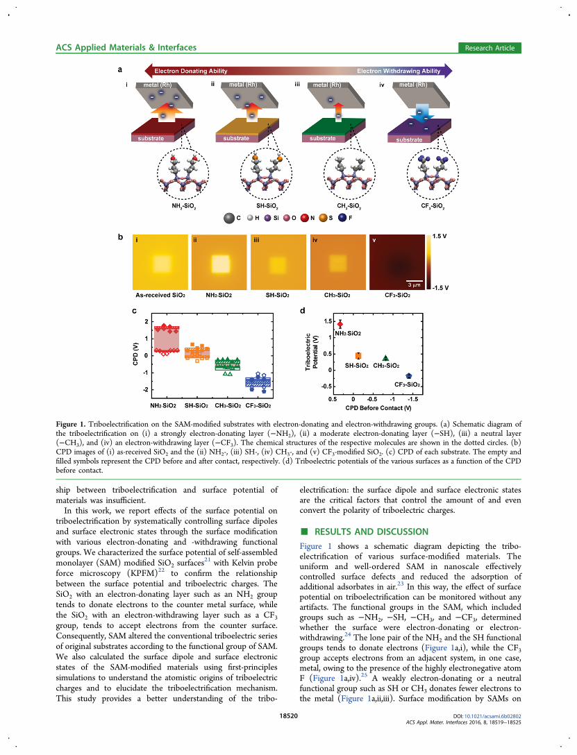
Figure 2. Atomistic origin of the generation of the triboelectric potential. (a) DOS of NH2−SiO2, SH−SiO2, CH3−SiO2, and CF3−SiO2 relative tothe vacuum level. (b) An excess electron of (i) NH2−SiO2 and (ii) CF3−SiO2, and a deficit electron of (iii) NH2−SiO2 and (iv) CF3−SiO2. (c)Energy band diagrams of substrates modified with a (i) NH2−SiO2, an electron-donating layer; (ii) CH3−SiO2, a neutral layer; (iii) CF3−SiO2, anelectron-withdrawing layer and that of the metal. EVAC and Δφ denote the vacuum level and the change of the surface dipole, respectively. The smallblack bars in the gap are the defect-induced surface states. The red bar in (i) and the violet bar in (iii) denote the SAM-induced surface states. TheSAM-induced surface dipoles are represented by the green circles. The directions of electron transfer are shown by arrows.
ACS Applied Materials & Interfaces Research Article
DOI: 10.1021/acsami.6b02802ACS Appl. Mater. Interfaces 2016, 8, 18519−18525
18521
constant and/or the mobile ions in it form a water bridge.27−29
However, the changes in the triboelectric potential caused bythe SAM were similar to those observed in dry N2. In addition,even though the SAM had identical functional group, thecarbon chain length of the SAM was also a factor affectingtriboelectrification owing to the formation of radicals along thecarbon chains (Figure S3, Supporting Information).30
To elucidate the triboelectrification process on the SAM-modified SiO2 surfaces, the surface dipole and surface statesinduced by the SAMs were estimated using a first-principlesmethod. Atomic structures were constructed by attaching theSAMs to the hydrogenated quartz (111) surface (Figure S4,Supporting Information). Then, the density of states (DOS)was calculated and plotted with respect to the vacuum level(Figure 2a). The black curves represent the total DOS, whilethe red ones represent the SAM-related portion of the totalDOS. There is around 1 eV difference between the total DOSof the NH2−SiO2 and CF3−SiO2 owing to the surface dipoledifference. The negative surface dipoles of NH2, SH, and CH3
groups reduced the surface potential, while the positive surfacedipole of CF3−SiO2 was along the direction in which thesurface potential increased (Table 1). Interestingly, among theSAM-modified surfaces with electron donating groups, theNH2−SiO2 and SH−SiO2 have the extra surface states (redpeaks) at approximately 5.5 eV in the gap, which further modifyits surface potential. These peaks were related to the loneelectron pair of the functional groups and we believe thesesurface states acted as the donor states. Although the dipole ofthe SH−SiO2 is smaller than that of the CH3−SiO2, thetriboelectric potential of the SH−SiO2 is larger than that of theCH3−SiO2 owing to these donor states. We confirmed the
surface dipole and the electronic states were varied by thefunctional group of SAM-modified surfaces, and the calculatedresults were in good agreements with the KPFM results. Thekey parameters from the experimental and computationalanalyses are listed in Table 1.Despite many studies on triboelectrification, it still remains
an unsolved issue where triboelectric charges are retained aftertriboelectrification. We investigated the spatial distribution ofan excess and a deficit electron after triboelectrification (Figure2b). It is extremely difficult to identify it even with the currentstate-of-art experimental techniques, but the first-principlesanalysis allows us to look over the charge distribution in theSAM-modified surfaces after triboelectrification. This chargedistribution was estimated from the difference in the electrondensities of the negatively/positively charged state and theneutral state. According to the KPFM results, the NH2−SiO2
lost electrons and became positively charged, while the CF3−SiO2 gained electrons and became negatively charged when theRh probe was contacted. When the NH2−SiO2 becomespositively charged, the lone-pair state of the nitrogen gives awayelectrons, as evidenced by the peak corresponding to theposition of the nitrogen (Figure 2b,i). On the contrary, whenthe CF3−SiO2 accepts electrons, electrons are accepted by theSiO2 surface, as the largest peak is at the surface of SiO2 and notat −CF3 or within the SiO2 substrate (Figure 2b,iv). On theother hand, electrons are accepted from and donated to thesurface of SiO2 when the NH2−SiO2 and the CF3−SiO2
becomes negatively and positively charged, respectively (Figure2b,iii,ii). Thus, the surface strongly affects not only the transferbut also the retention of triboelectric charges after tribo-electrification.
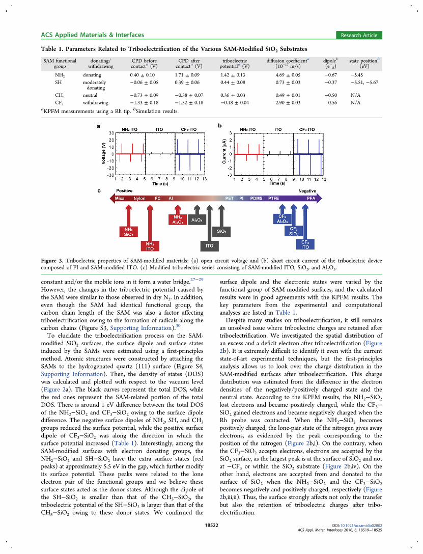
Table 1. Parameters Related to Triboelectrification of the Various SAM-Modified SiO2 Substrates
SAM functionalgroup
donating/withdrawing
CPD beforecontacta (V)
CPD aftercontacta (V)
triboelectricpotentiala (V)
diffusion coefficienta
(10−17 m/s)dipoleb
(e−Å)state positionb
(eV)
NH2 donating 0.40 ± 0.10 1.71 ± 0.09 1.42 ± 0.13 4.69 ± 0.05 −0.67 −5.45SH moderately
donating−0.06 ± 0.05 0.39 ± 0.06 0.44 ± 0.08 0.73 ± 0.03 −0.37 −5.51, −5.67
CH3 neutral −0.73 ± 0.09 −0.38 ± 0.07 0.36 ± 0.03 0.49 ± 0.01 −0.50 N/ACF3 withdrawing −1.33 ± 0.18 −1.52 ± 0.18 −0.18 ± 0.04 2.90 ± 0.03 0.56 N/A
aKPFM measurements using a Rh tip. bSimulation results.
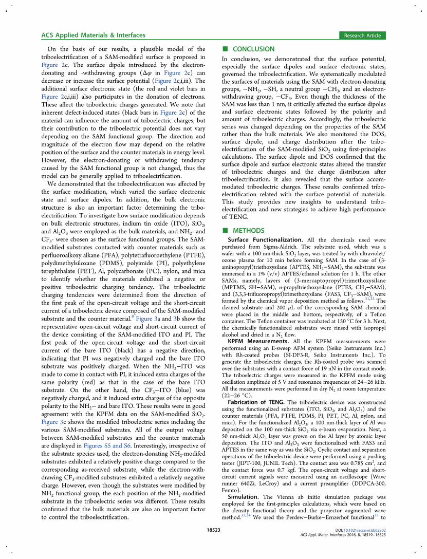
Figure 3. Triboelectric properties of SAM-modified materials: (a) open circuit voltage and (b) short circuit current of the triboelectric devicecomposed of PI and SAM-modified ITO. (c) Modified triboelectric series consisting of SAM-modified ITO, SiO2, and Al2O3.
ACS Applied Materials & Interfaces Research Article
DOI: 10.1021/acsami.6b02802ACS Appl. Mater. Interfaces 2016, 8, 18519−18525
18522
On the basis of our results, a plausible model of thetriboelectrification of a SAM-modified surface is proposed inFigure 2c. The surface dipole introduced by the electron-donating and -withdrawing groups (Δφ in Figure 2c) candecrease or increase the surface potential (Figure 2c,i,iii). Theadditional surface electronic state (the red and violet bars inFigure 2c,i,iii) also participates in the donation of electrons.These affect the triboelectric charges generated. We note thatinherent defect-induced states (black bars in Figure 2c) of thematerial can influence the amount of triboelectric charges, buttheir contribution to the triboelectric potential does not varydepending on the SAM functional group. The direction andmagnitude of the electron flow may depend on the relativeposition of the surface and the counter materials in energy level.However, the electron-donating or withdrawing tendencycaused by the SAM functional group is not changed, thus themodel can be generally applied to triboelectrification.We demonstrated that the triboelectrification was affected by
the surface modification, which varied the surface electronicstate and surface dipoles. In addition, the bulk electronicstructure is also an important factor determining the tribo-electrification. To investigate how surface modification dependson bulk electronic structures, indium tin oxide (ITO), SiO2,and Al2O3 were employed as the bulk materials, and NH2- andCF3- were chosen as the surface functional groups. The SAM-modified substrates contacted with counter materials such asperfluoroalkoxy alkane (PFA), polytetrafluoroethylene (PTFE),polydimethylsiloxane (PDMS), polyimide (PI), polyethyleneterephthalate (PET), Al, polycarbonate (PC), nylon, and micato identify whether the materials exhibited a negative orpositive triboelectric charging tendency. The triboelectriccharging tendencies were determined from the direction ofthe first peak of the open-circuit voltage and the short-circuitcurrent of a triboelectric device composed of the SAM-modifiedsubstrate and the counter material.8 Figure 3a and 3b show therepresentative open-circuit voltage and short-circuit current ofthe device consisting of the SAM-modified ITO and PI. Thefirst peak of the open-circuit voltage and the short-circuitcurrent of the bare ITO (black) has a negative direction,indicating that PI was negatively charged and the bare ITOsubstrate was positively charged. When the NH2−ITO wasmade to come in contact with PI, it induced extra charges of thesame polarity (red) as that in the case of the bare ITOsubstrate. On the other hand, the CF3−ITO (blue) wasnegatively charged, and it induced extra charges of the oppositepolarity to the NH2− and bare ITO. These results were in goodagreement with the KPFM data on the SAM-modified SiO2.Figure 3c shows the modified triboelectric series including thevarious SAM-modified substrates. All of the output voltagebetween SAM-modified substrates and the counter materialsare displayed in Figures S5 and S6. Interestingly, irrespective ofthe substrate species used, the electron-donating NH2-modifedsubstrates exhibited a relatively positive charge compared to thecorresponding as-received substrate, while the electron-with-drawing CF3-modified substrates exhibited a relatively negativecharge. However, even though the substrates were modified byNH2 functional group, the each position of the NH2-modifiedsubstrate in the triboelectric series was different. These resultsconfirmed that the bulk materials are also an important factorto control the triboelectrification.
■ CONCLUSIONIn conclusion, we demonstrated that the surface potential,especially the surface dipoles and surface electronic states,governed the triboelectrification. We systematically modulatedthe surfaces of materials using the SAM with electron-donatinggroups, −NH2, −SH, a neutral group −CH3, and an electron-withdrawing group, −CF3. Even though the thickness of theSAM was less than 1 nm, it critically affected the surface dipolesand surface electronic states followed by the polarity andamount of triboelectric charges. Accordingly, the triboelectricseries was changed depending on the properties of the SAMrather than the bulk materials. We also monitored the DOS,surface dipole, and charge distribution after the tribo-electrification of the SAM-modified SiO2 using first-principlescalculations. The surface dipole and DOS confirmed that thesurface dipole and surface electronic states altered the transferof triboelectric charges and the charge distribution aftertriboelectrification. It also revealed that the surface accom-modated triboelectric charges. These results confirmed tribo-electrification related with the surface potential of materials.This study provides new insights to understand tribo-electrification and new strategies to achieve high performanceof TENG.
■ METHODSSurface Functionalization. All the chemicals used were
purchased from Sigma-Aldrich. The substrate used, which was awafer with a 100 nm-thick SiO2 layer, was treated by with ultraviolet/ozone plasma for 10 min before forming SAM. In the case of (3-aminopropyl)triethoxysilane (APTES, NH2−SAM), the substrate wasimmersed in a 1% (v/v) APTES/ethanol solution for 1 h. The otherSAMs, namely, layers of (3-mercaptopropyl)trimethoxysilane(MPTMS, SH−SAM), n-propyltriethoxysilane (PTES, CH3−SAM),and (3,3,3-trifluoropropyl)trimethoxysilane (FAS3, CF3−SAM), wereformed by the chemical vapor deposition method as follows.31,32 Thecleaned substrate and 200 μL of the corresponding SAM chemicalwere placed in the middle and bottom, respectively, of a Tefloncontainer. The Teflon container was incubated at 150 °C for 3 h. Next,the chemically functionalized substrates were rinsed with isopropylalcohol and dried in a N2 flow.
KPFM Measurements. All the KPFM measurements wereperformed using an E-sweep AFM system (Seiko Instruments Inc.)with Rh-coated probes (SI-DF3-R, Seiko Instruments Inc.). Togenerate the triboelectric charges, the Rh-coated probe was scannedover the substrates with a contact force of 19 nN in the contact mode.The triboelectric charges were measured in the KPFM mode usingoscillation amplitude of 5 V and resonance frequencies of 24−26 kHz.All the measurements were performed in dry N2 at room temperature(22−26 °C).
Fabrication of TENG. The triboelectric device was constructedusing the functionalized substrates (ITO, SiO2, and Al2O3) and thecounter materials (PFA, PTFE, PDMS, PI, PET, PC, Al, nylon, andmica). For the functionalized Al2O3, a 100 nm-thick layer of Al wasdeposited on the 100 nm-thick SiO2 via e-beam evaporation. Next, a50 nm-thick Al2O3 layer was grown on the Al layer by atomic layerdeposition. The ITO and Al2O3 were functionalized with FAS3 andAPTES in the same way as was the SiO2. Cyclic contact and separationoperations of the triboelectric device were performed using a pushingtester (JIPT-100, JUNIL Tech). The contact area was 0.785 cm2, andthe contact force was 0.7 kgf. The open-circuit voltage and short-circuit current signals were measured using an oscilloscope (Waverunner 640Zi, LeCroy) and a current preamplifier (DDPCA-300,Femto).
Simulation. The Vienna ab initio simulation package wasemployed for the first-principles calculations, which were based onthe density functional theory and the projector augmented wavemethod.33,34 We used the Perdew−Burke−Ernzerhof functional35 to
ACS Applied Materials & Interfaces Research Article
DOI: 10.1021/acsami.6b02802ACS Appl. Mater. Interfaces 2016, 8, 18519−18525
18523
describe the exchange and correlation effects of electrons. The plane-wave cutoff was 400 eV. Only the gamma point was sampled for ionicrelaxation, whereas a 5 × 5 × 1 Monkhorst−Pack k-point grid36 wassampled for the DOS. The SiO2 slab was adopted from the literature.37
The unit cell included a vacuum of at least 15 Å to minimize spuriousinteractions between the cells. The surface dipoles were computedfrom the charge distribution after correcting the potential due tospurious interaction between cells.
■ ASSOCIATED CONTENT*S Supporting InformationThe Supporting Information is available free of charge on theACS Publications website at DOI: 10.1021/acsami.6b02802.
Diffusion of triboelectric charges on various surfaces,triboelectrification in air, triboelectrification of CH3−SiO2 with different carbon chain length, unit cell used indensity of functional theory calculations, and outputvoltage between SAM-modified substrates and thecounter materials (PDF)
■ AUTHOR INFORMATIONCorresponding Authors*E-mail: [email protected].*E-mail: [email protected].*E-mail: [email protected] ContributionsK.-E.B. and Y.C. contributed equally to this work. H.-J.S. andS.P. designed the study and were responsible for projectplanning. K.-E.B. performed most of the surface treatment andthe fabrication of the TENG. Y.C. performed the computa-tional simulations. M.S. and S.K. helped with the fabrication ofthe TENG and data analysis. S.-W.K. and S.H. participated inthe discussion. S.-W.K., H.-J.S., and S.P. cowrote the manu-script.NotesThe authors declare no competing financial interest.
■ ACKNOWLEDGMENTSThis work was financially supported by Basic Science ResearchProgram (Grant 2015R1A2A1A05001851) through the Na-tional Research Foundation (NRF) of Korea Grant funded bythe Ministry of Science, ICT & Future Planning.
■ REFERENCES(1) Voldman, S. H. ESD Physics and Devices, 1st ed.; Wiley: WestSussex, U.K., 2005.(2) Pai, D. M.; Springett, B. E. Physics of Electrophotography. Rev.Mod. Phys. 1993, 65, 163−211.(3) Bittner, J. D.; Hrach, F. J.; Gasiorowski, S. A.; Canellopoulus, L.A.; Guicherd, H. Triboelectric Belt Separator for Beneficiation of FineMinerals. Procedia Eng. 2014, 83, 122−129.(4) Inculet, I. I. Electrostatics in Industry. J. Electrost. 1978, 4, 175−192.(5) Lin, L.; Xie, Y.; Wang, S.; Wu, W.; Niu, S.; Wen, X.; Wang, Z. L.Triboelectric Active Sensor Array for Self-Powered Static and DynamicPressure Detection and Tactile Imaging. ACS Nano 2013, 7, 8266−8274.(6) Wang, S.; Lin, L.; Wang, Z. L. Nanoscale Triboelectric-Effect-Enabled Energy Conversion for Sustainably Powering PortableElectronics. Nano Lett. 2012, 12, 6339−6346.(7) Seung, W.; Gupta, M. K.; Lee, K. Y.; Shin, K.; Lee, J.; Kim, T. Y.;Kim, S.; Lin, J.; Kim, J. H.; Kim, S. Nanopatterned Textile-BasedWearable Triboelectric Nanogenerator. ACS Nano 2015, 9, 3501−3509.
(8) Zhu, G.; Pan, C.; Guo, W.; Chen, C. Y.; Zhou, Y.; Yu, R.; Wang,Z. L. Triboelectric-Generator-Driven Pulse Electrodeposition forMicropatterning. Nano Lett. 2012, 12, 4960−4965.(9) Zhu, G.; Lin, Z. H.; Jing, Q.; Bai, P.; Pan, C.; Yang, Y.; Zhou, Y.;Wang, Z. L. Toward Large-Scale Energy Harvesting by a Nanoparticle-Enhanced Triboelectric Nanogenerator. Nano Lett. 2013, 13, 847−853.(10) Bai, P.; Zhu, G.; Lin, Z. H.; Jing, Q.; Chen, J.; Zhang, G.; Ma, J.;Wang, Z. L. Integrated Multilayered Triboelectric Nanogenerator forHarvesting Biomechanical Energy from Human Motions. ACS Nano2013, 7, 3713−3719.(11) Zhu, G.; Chen, J.; Liu, Y.; Bai, P.; Zhou, Y. S.; Jing, Q.; Pan, C.;Wang, Z. L. Linear-Grating Triboelectric Generator Based on SlidingElectrification. Nano Lett. 2013, 13, 2282−2289.(12) Lowell, J.; Rose-Innes, A. C. Contact Electrification. Adv. Phys.1980, 29, 947−1023.(13) Lee, L.-H. Dual Mechanism for Metal-Polymer ContactElectrification. J. Electrost. 1994, 32, 1−29.(14) Smith, J. R. Self-Consistent Many-Electron Theory of ElectronWork Functions and Surface Potential Characteristics for SelectedMetals. Phys. Rev. 1969, 181, 522−529.(15) Monch, W. Semiconductor Surfaces and Interfaces, 3rd ed.;Springer: Berlin, Germany, 1995.(16) Bailey, A. G. The Charging of Insulator Surfaces. J. Electrost.2001, 51−52, 82−90.(17) Galembeck, F.; Burgo, T. A. L.; Balestrin, L. B. S.; Gouveia, R.F.; Silva, C. A.; Galembeck, A. Friction, Tribochemistry andTriboelectricity: Recent Progress and Perspectives. RSC Adv. 2014,4, 64280−64298.(18) Song, G.; Kim, Y.; Yu, S.; Kim, M.-O.; Park, S.-H.; Cho, S. M.;Velusamy, D. B.; Cho, S. H.; Kim, K. L.; Kim, J.; Kim, E.; Park, C.Molecularly Engineered Surface Triboelectric Nanogenerator by Self-Assembled Monolayers (METS). Chem. Mater. 2015, 27, 4749−4755.(19) Wang, S.; Zi, Y.; Zhou, Y. S.; Li, S.; Fan, F.; Lin, L.; Wang, Z. L.Molecular Surface Functionalization to Enhance the Power Output ofTriboelectric Nanogenerators. J. Mater. Chem. A 2016, 4, 3728−3734.(20) Horn, R. G.; Smith, D. T.; Grabbe, A. Contact ElectrificationInduced by Monolayer Modification of a Surface and Relation to Acid-Base Interactions. Nature 1993, 366, 442−443.(21) Ulman, A. Formation and Structure of Self-AssembledMonolayers. Chem. Rev. 1996, 96, 1533−1554.(22) Melitz, W.; Shen, J.; Kummel, A. C.; Lee, S. Kelvin Probe ForceMicroscopy and Its Application. Surf. Sci. Rep. 2011, 66, 1−27.(23) Rimola, A.; Costa, D.; Sodupe, M.; Lambert, J.-F.; Ugliengo, P.Silica Surface Features and Their Role in the Adsorption ofBiomolecules: Computational Modeling and Experiments. Chem.Rev. 2013, 113, 4216−4313.(24) Shin, H. J.; Soo, M. K.; Yoon, S. M.; Benayad, A.; Ki, K. K.;Sung, J. K.; Hyun, K. P.; Choi, J. Y.; Young, H. L. Tailoring ElectronicStructures of Carbon Nanotubes by Solvent with Electron-Donatingand -Withdrawing Groups. J. Am. Chem. Soc. 2008, 130, 2062−2066.(25) Carey, F. A. Organic Chemistry, 4th ed.; McGraw-Hill College:Boston, MA, 2000.(26) Zhou, Y. S.; Liu, Y.; Zhu, G.; Lin, Z. H.; Pan, C.; Jing, Q.; Wang,Z. L. In Situ Quantitative Study of Nanoscale Triboelectrification andPatterning. Nano Lett. 2013, 13, 2771−2776.(27) McCarty, L. S.; Winkleman, A.; Whitesides, G. M. IonicElectrets: Electrostatic Charging of Surfaces by Transferring MobileIons upon Contact. J. Am. Chem. Soc. 2007, 129, 4075−4088.(28) Adamson, A. W.; Gast, A. P. Physical Chemistry of Surfaces, 6thed.; Wiley: New York, 1997.(29) Pence, S.; Novotny, V. J.; Diaz, A. F. Effect of Surface Moistureon Contact Charge of Polymers Containing Ions. Langmuir 1994, 10,592−596.(30) Baytekin, B.; Baytekin, H. T.; Grzybowski, B. a. What ReallyDrives Chemical Reactions on Contact Charged Surfaces? J. Am.Chem. Soc. 2012, 134, 7223−7226.(31) Hayashi, K.; Saito, N.; Sugimura, H.; Takai, O.; Nakagiri, N.Surface Potential Contrasts between Silicon Surfaces Covered and
ACS Applied Materials & Interfaces Research Article
DOI: 10.1021/acsami.6b02802ACS Appl. Mater. Interfaces 2016, 8, 18519−18525
18524
Uncovered with an Organosilane Self-Assembled Monolayer. Ultra-microscopy 2002, 91, 151−156.(32) Hozumi, A.; Ushiyama, K.; Sugimura, H.; Takai, O.Fluoroalkylsilane Monolayers Formed by Chemical Vapor SurfaceModification on Hydroxylated Oxide Surfaces. Langmuir 1999, 15,7600−7604.(33) Blochl, P. E. Projector Augmented-Wave Method. Phys. Rev. B:Condens. Matter Mater. Phys. 1994, 50, 17953−17979.(34) Kresse, G.; Furthmuller, J. Efficient Iterative Schemes for AbInitio Total-Energy Calculations Using a Plane-Wave Basis Set. Phys.Rev. B: Condens. Matter Mater. Phys. 1996, 54, 11169−11186.(35) Perdew, J. P.; Burke, K.; Ernzerhof, M. Generalized GradientApproximation Made Simple. Phys. Rev. Lett. 1996, 77, 3865−3868.(36) Monkhorst, H. J.; Pack, J. D. Special Points for Brillouin-ZoneIntegrations. Phys. Rev. B 1976, 13, 5188−5192.(37) Goumans, T. P. M.; Wander, A.; Brown, W. A.; Catlow, C. R. A.Structure and Stability of the (001) Alpha-Quartz Surface. Phys. Chem.Chem. Phys. 2007, 9, 2146−2152.
ACS Applied Materials & Interfaces Research Article
DOI: 10.1021/acsami.6b02802ACS Appl. Mater. Interfaces 2016, 8, 18519−18525
18525