Embed Size (px)
Citation preview

DesignCon 2009
Control of Electromagnetic Radiation from Integrated Circuit Heat sinks Cristian Tudor, Fidus Systems Inc. [email protected] Syed. A. Bokhari, Fidus Systems Inc. [email protected]

Abstract A common approach to reducing radiated emissions from heat sinks is multi-point grounding. These reduce PCB routing area and can become difficult and impractical in some cases. This paper examines the effect of using a Dissipative Edge Termination (DET) scheme. This consists of resistive loading of the edges of the heat sink. Analysis carried out using a 3D EM field solver shows that a 10-20 dB of reduction in the near field strength is feasible with a proper choice of resistance. Heat sinks of the bi-directional and omni-directional type have been analyzed in detail and the advantages and limitations of this method are presented.
Author(s) Biography Cristian Tudor is currently a senior signal integrity engineer with Fidus Systems Inc, Ottawa, Canada. His work includes analog simulations of high speed interfaces, interconnect modeling, characterization and optimization. He is also engaged in the design and characterization of power distribution networks, SSO analysis, and jitter analysis both at board as well as microcircuit level. Prior to joining Fidus, Cristian was part of the engineering staff at Nortel Networks and Chipworks Inc. He was involved in signal integrity and patent analysis related to integrated circuits. Cristian holds an M.Sc diploma in Electrical Engineering from the Polytechnic University, Bucharest, Romania. Syed Bokhari received a Ph.D degree in Electrical Engineering from the Indian Institute of Science, Bangalore, India. He is currently a Lead Signal Integrity and EMC specialist at Fidus Systems Inc. He has over 20 years experience, primarily in the area of electromagnetic modeling. His previous academic employers include Ecole Polytechnic Federale de Lausanne in Switzerland, and the University of Ottawa in Canada. He has worked in the industry at the Indian Space Research Organization, and at Cadence Design Systems (Canada) Ltd. He has over 50 publications, contributed to chapters in books and holds one patent. He is a senior member of the IEEE and is the chairman of the Ottawa EMC chapter. His areas of current interest include interconnect modeling for SI and EMC, and miniaturized antenna design.
Introduction Cooling of large Integrated Circuits (ICs) is most commonly done using heat sinks. It is known that their proximity to IC circuitry carrying high speed signals enhances radiation. This can cause products to fail EMC regulations in the GHz range. Many methods have been developed to reduce the amplitude of the field scattered by a heatsink. In [1], a design flow is presented where some physical parameter of the heatsink, such as the number of fins is modified to avoid major resonance peaks in the frequency range of interest. In general, the mechanism of radiation from a heatsink is similar that of a Printed Circuit Board (PCB) Power-Ground plane pair. This topic has been well researched for Signal and Power Integrity and the solutions developed to improve performance also help in reducing emissions. In [2], an impedance matched lossy decoupling termination has been used for improving signal integrity. Another method consists of surrounding the Power and Ground plane edges with an absorbing material [3]. Use of multi-point grounding [4] is a common method that increases the lowest resonant frequency of the heat sink. By a proper location and by increasing the number of grounds, the lowest resonant frequency can be pushed beyond the frequency range of interest. The problem of interest is the near field radiation of the heatsink. Printed Circuit Boards (PCBs) containing large Ball Grid Arrays (BGAs) with Gbps data rates such PCI-Express, XAUI, 10G Base – KR, etc. are invariably housed in shielded enclosures. Direct far field radiation from the heat sink is not possible, but the presence of apertures in the near field of the heatsink leads to secondary radiation. In these high speed BGAs, there are a large number of differential pairs concentrated at the periphery. Consequently, this region is prime real estate for surface routing, series termination resistors, AC coupling capacitors, and decoupling capacitors. The method described in [1] has the advantage that it does not affect the PCB component placement and routing. However, heat sink size adjustments can only provide a limited control without sacrificing its thermal performance. Use of an absorber as in [3] requires a considerable amount of the PCB surface area near the IC, but is expected to yield a significant reduction in emissions. Both [2] and [4] require multiple heat sink connections to the PCB surface. The work described in this paper is inspired by the techniques [2,4] and [3]. A combination gives a solution that reduces the near field radiation by a substantial amount while requiring a small area around the IC. Its advantage has been proven for Power-Ground pair radiation [5]. The method consists of using a purely resistive termination at a minimum number of locations around the IC. By a proper choice of the value of resistance, significant emission reduction is possible at the resonant frequencies of the heatsink of the bi-directional type. Further, a realistic heat sink excitation model and a detailed analysis of two common types of heatsinks is carried out. Numerical results are generated using a 3D EM field solver (Ansoft’s HFSS [6]).

A two dimensional heatsink model A better understanding of heat sink resonances and radiation is obtained by using a “2D model” as shown in Figure 1. This is basically a section of a flat 3 dimensional heatsink with the fins removed. It is placed on a 200 x 200 mm perfectly conducting ground plane the excitation is provided with lumped gap constant voltage source (1 Volt) as in a probe fed microstrip patch antenna. The near field components of this geometry are computed over a hemisphere of radius = 40 mm. The sum of the magnitudes of the electric field components (Etotal) is computed over the hemisphere and the maximum value (Max Near Etotal) is used as the figure of merit. It is expressed in decibels.
Figure 1: Geometry of a “2D model of a heat sink (dimensions in mm)
The input impedance and Max Near Etotal are shown in Figure 2 as a function of the frequency. Near field radiation has a maximum at the resonant frequencies which is also the frequencies of lowest impedance. Maximum current flows at these frequencies causing increased radiation. For the geometry as in Figure 2, fins are added as shown in Figure 3. Computed near field and impedance results are shown in Figure 4. Near field behavior is similar to that of Figure 2 with some important differences. First, the dominant resonant frequency reduces and multiple resonances are seen. The first three near field maxima in this case are similar to those in Figure 2 are also associated with impedance minima. These are due to resonances along the length of the heatsink (the horizontal member). Near field peaks in the frequency range of 4 to 5 GHz appear due to resonances of the fins that act like

quarter wave monopoles. These resonances, unlike the first 3 that are associated with microstrip cavity type resonances, are of a narrow band nature. Their importance is illustrated in the 3D examples below.
Figure 2: Input impedance and peak total near field of the geometry in Figure 2.
Figure 3: Geometry of a “2D model of a heat sink with fins (dimensions in mm)

Figure 4: Input impedance and peak total near field of the geometry in Figure 3.
Heatsink excitation Model
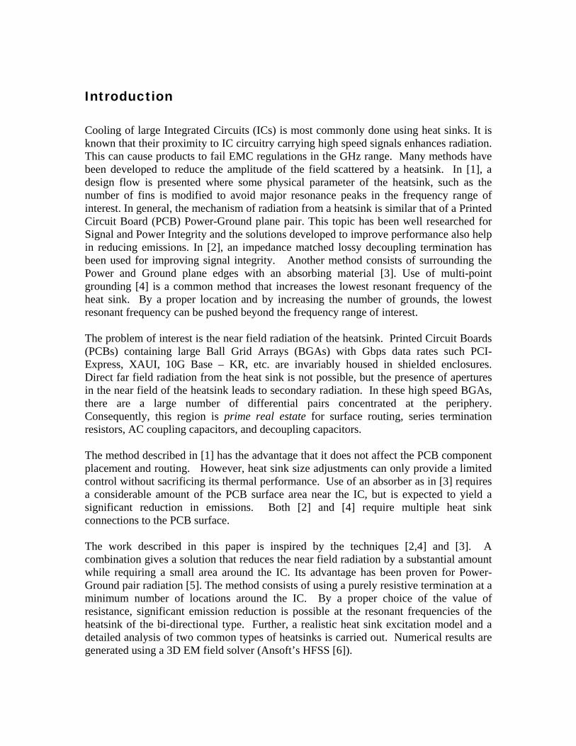
The excitation model used in Figures 1, and 3 will show high emission levels as the input signal is directly coupled to the heat sink. In reality, coupling is electromagnetic and a better model is a small loop placed under the heat sink (Figure 5). Further, the near environment of the die can be very complex. It may be encapsulated, contain heat spreaders and have a complex ceramic package underneath. For simplicity, it is assumed that the small loop is encapsulated in a rectangular dielectric slab made of Polyimide material as shown in Figure 5. The small square loop has its center located at the coordinates (2,2,2) mm. It is intentionally offset along x- and y axes to enable excitation of all possible resonance modes. A lumped gap constant voltage source (1 Volt) is used at the gap of the loop. The input impedance of the loop is largely inductive and is not shown here. Near fields of the loop alone embedded in the polyimide slab and placed over a 200 x 200 mm perfectly conducting plane are computed over the hemisphere of radius = 40 mm. The maximum value is plotted as a function of the frequency in Figure 6. This is treated as a reference and is used to compare heatsink radiations.
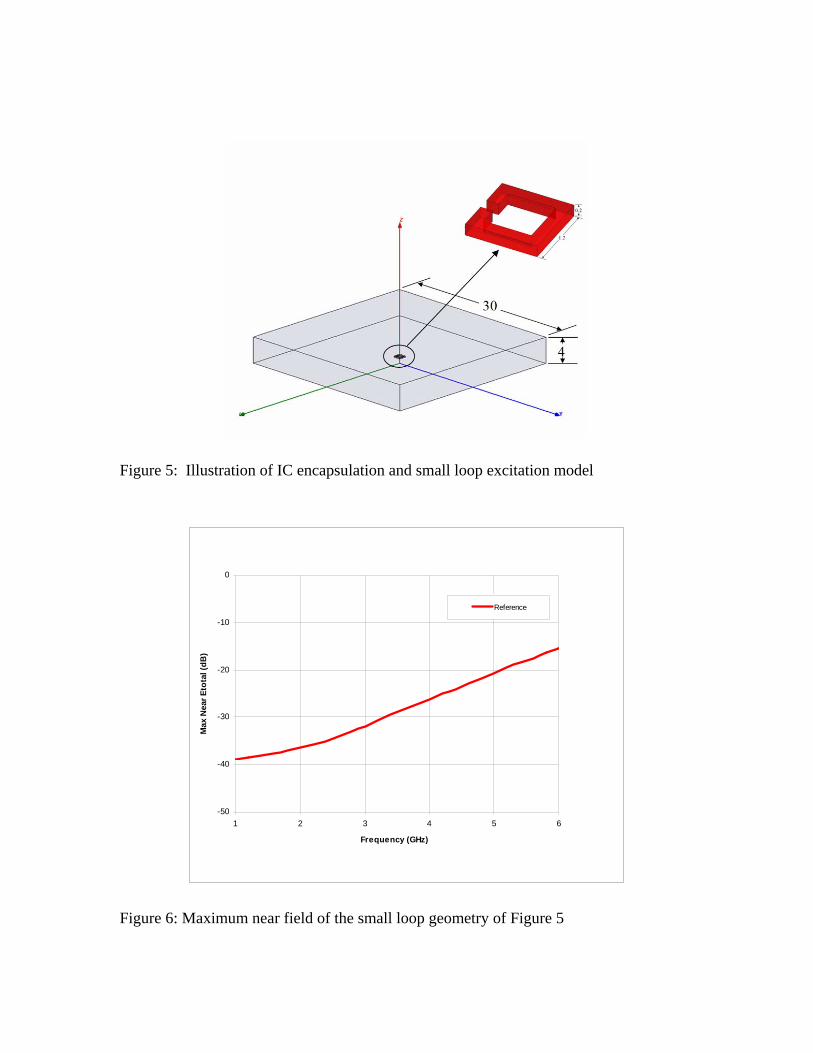
Figure 5: Illustration of IC encapsulation and small loop excitation model
-50
-40
-30
-20
-10
0
1 2 3 4 5 6
Frequency (GHz)
Max
Nea
r Eto
tal (
dB)
Reference
Figure 6: Maximum near field of the small loop geometry of Figure 5

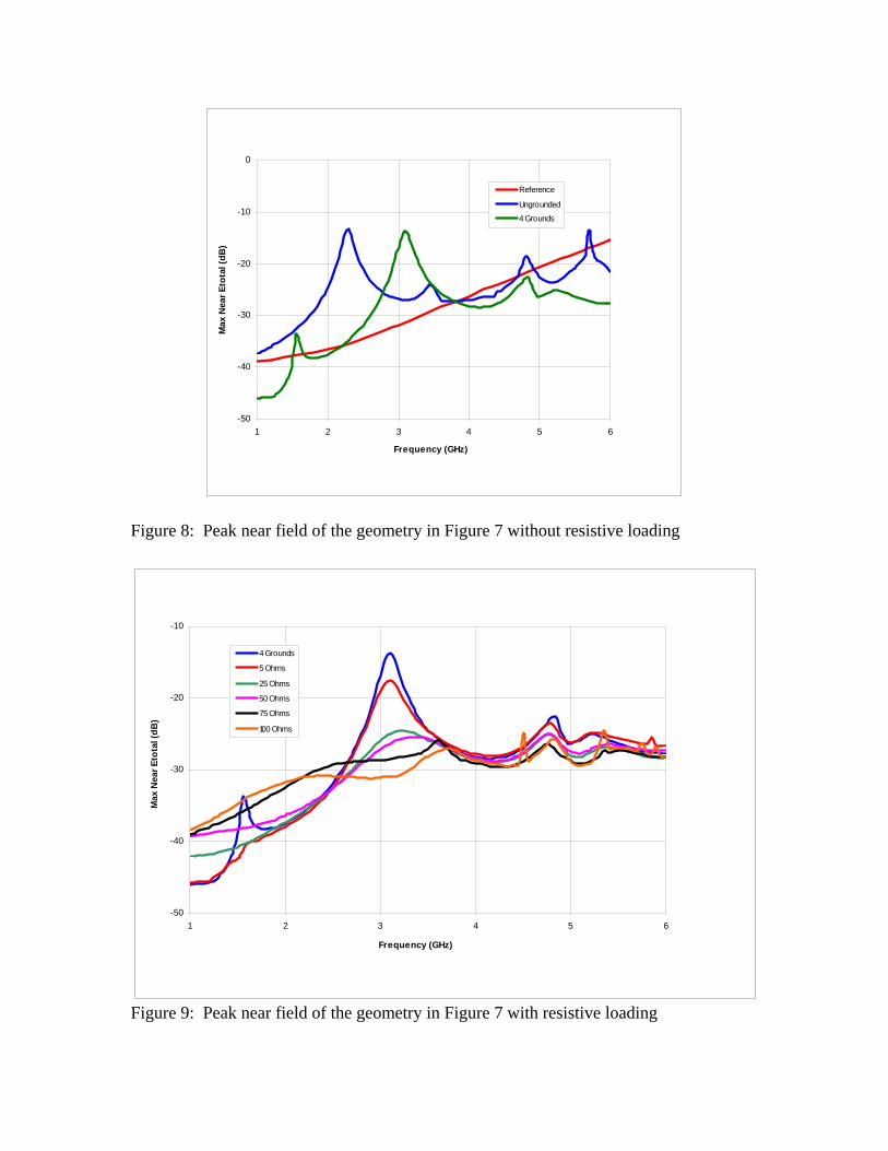
Resistive loading Resistive loading is implemented by connecting the heatsink base to the ground plane on the top surface of the PCB through a series resistor. This is simulated by introducing a pillar between the base of the heatsink and the perfectly conducting ground plane as shown in the inset in Figure 7. The pillar has a square cross section of side length = 1mm, and height = 3.8 mm. A 0.2 mm high rectangular sheet is used to represent a lumped resistive element. Making the value of resistance equal to zero amounts to grounding the heatsink. In essence, resistive loading is more general than grounding. Further, in all illustrations below, only four pillars placed at the corners of the heat sink are considered. This is a convenient location for grounding and resistive loading as it will not be in the direct path of the high speed traces. Bi-directional Heatsink This is one of the most common types of heatsink meant for usage where the airflow is bi-directional. The fins are rectangular plates and a typical configuration with a small number of fins is shown in Figure 7. The heat sink base is a square slab of side length = 36 mm and thickness = 2 mm. The fin thickness is 1.5 mm. The material is assumed to be copper. The polyimide encapsulation is placed between the heatsink base and a perfectly conducting ground plane. Simulation results without resistive loading are shown in Figure 8. The curve marked “reference” is the radiation from the square loop used as the excitation embedded in a polyimide slab (Figure 5). The ungrounded case corresponds to one where the 4 pillars are removed. The curve labeled “4 grounds” corresponds to the case where the 4 pillars are present and the resistance is set to zero. First, it can be seen that radiation increases significantly at the resonant frequencies of the ungrounded heatsink. Grounding the heatsink at the four corners reduces the radiation level at the first resonance of the ungrounded heatsink. However, an increased radiation at ~3 GHz is seen. To reduce this peak, more ground connections will be needed. The effect of resistive loading is shown in Figure 9. The “4 grounds” case of Figure 7 is repeated for comparison. The curve labeled “5 Ohms” corresponds to the case where each pillar was loaded with a 5 Ohms resistor. It can be seen that increasing the value of resistance decreases the radiation level at the resonant frequencies. It however increases the radiation level in the low frequency range. A value of 50 -100 Ohms is very effective. As the value of resistance is increased further, the heat sink radiation will begin to approach that of the ungrounded case and the advantage of resistive loading gradually disappears. In a second example, a bi-directional heatsink with a higher fin density is considered as shown in Figure 10. Simulation results are shown In Figure 11. It can be seen that a 50 Ohm resistive loading proves to be effective. Both resistive loading as well as grounding are useful in situations where the resonances cause a dominant current flow on the base of the heatsink. Figure 12 shows the surface

current density of the ungrounded heatsink at its first resonance of 2.3 GHz. Maximum current density at the base of the heat sink can be seen. Figure 13 shows the surface current density of the grounded heatsink at 3 GHz. Again, it can be seen that the maximum surface current is essentially in the base and the ground pillars. Consequently, resistive loading can help reduce radiation. There are certain heat sink resonance modes where the maximum current need not be on the base of the heatsink. For the example in illustration, resonances that appear above 5 GHz are associated with maximum current flowing on the fins. These are very difficult to control with either resistive loading or grounding. A significant increase in the number of grounding locations is required in this case. An interesting observation of the results in Figure 9 for 100 Ohm resistance value shows spurious resonances at frequencies above 4 GHz. As such making the resistance higher will not reproduce results of the ungrounded case. This is due to the capacitance between the pillars and the ground plane. This means that the resistor element used to implement resistive loading must ensure a very low shunt capacitance. Examination of the effect of of shunt capacitance on a resistively loaded heat sink is shown in Figure 14. It can be seen that shunt capacitance values of 2 pF will destroy the benefit of resistive loading. Shunt capacitance values need to be 0.5 pF or less to make resistive loading effective.
Figure 7: Geometry of a bi-directional heatsink with 7 fins
-50
-40
-30
-20
-10
0
1 2 3 4 5 6
Frequency (GHz)
Max
Nea
r Eto
tal (
dB)
Reference
Ungrounded
4 Grounds
Figure 8: Peak near field of the geometry in Figure 7 without resistive loading
-50
-40
-30
-20
-10
1 2 3 4 5 6
Frequency (GHz)
Max
Nea
r Eto
tal (
dB)
4 Grounds
5 Ohms
25 Ohms
50 Ohms
75 Ohms
100 Ohms
Figure 9: Peak near field of the geometry in Figure 7 with resistive loading

Figure 10: Geometry of a bi-directional heatsink with 19 fins (fin thickness = 1 mm)
-50
-40
-30
-20
-10
0
10
1 1.5 2 2.5 3 3.5 4 4.5 5 5.5 6
Frequency (GHz)
Max
Nea
r Eto
tal (
dB)
4 Grounds
50 Ohms
Figure 11: Peak near field of the geometry in Figure 10 with resistive loading
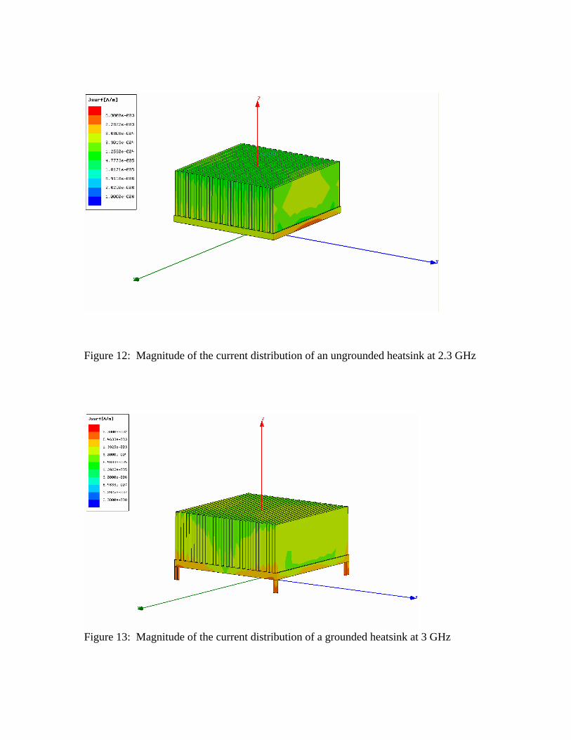
Figure 12: Magnitude of the current distribution of an ungrounded heatsink at 2.3 GHz
Figure 13: Magnitude of the current distribution of a grounded heatsink at 3 GHz

-50
-40
-30
-20
-10
1 1.5 2 2.5 3 3.5 4 4.5 5 5.5 6
Frequency (GHz)
Max
Nea
r Eto
tal (
dB)
0 pF
2 pF
1 pF
0.5 pF
Figure 14: Peak near field of the geometry in Figure 10 with resistive load of 50 Ohms and for various values of shunt capacitance. Omni-directional Heatsinks
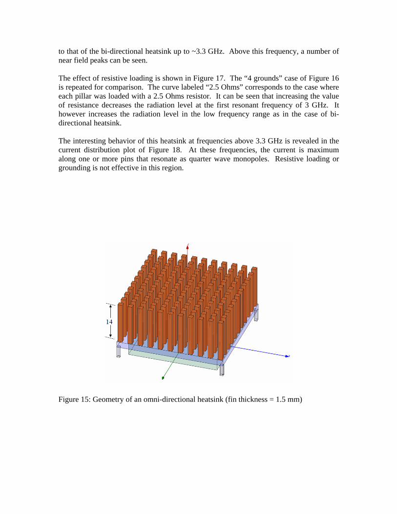
This is another common type of heatsink meant for usage where the airflow is omni-directional. It is also known as a pin fin heatsink (Figure 15). The heat sink base is a square slab of side length = 36 mm and thickness = 2 mm. The fin thickness is 1.5 mm. The material is assumed to be copper. The polyimide encapsulation is placed between the heatsink base and a perfectly conducting ground plane. Simulation results without resistive loading are shown in Figure 16. The curve marked reference is the radiation from the square loop used as the excitation embedded in a polyimide slab (Figure 5). The ungrounded case corresponds to one where the 4 pillars are removed. The curve labeled “4 grounds” corresponds to the case where the 4 pillars are present and the resistance is set to zero. First, it can be seen again that radiation increases significantly at the resonant frequencies of the ungrounded heatsink. Grounding the heatsink at the four corners reduces the radiation level at the first dominant resonance frequency of the ungrounded heatsink. The behavior is very similar
to that of the bi-directional heatsink up to ~3.3 GHz. Above this frequency, a number of near field peaks can be seen. The effect of resistive loading is shown in Figure 17. The “4 grounds” case of Figure 16 is repeated for comparison. The curve labeled “2.5 Ohms” corresponds to the case where each pillar was loaded with a 2.5 Ohms resistor. It can be seen that increasing the value of resistance decreases the radiation level at the first resonant frequency of 3 GHz. It however increases the radiation level in the low frequency range as in the case of bi-directional heatsink. The interesting behavior of this heatsink at frequencies above 3.3 GHz is revealed in the current distribution plot of Figure 18. At these frequencies, the current is maximum along one or more pins that resonate as quarter wave monopoles. Resistive loading or grounding is not effective in this region.
Figure 15: Geometry of an omni-directional heatsink (fin thickness = 1.5 mm)

-40
-30
-20
-10
0
10
1 2 3 4 5 6
Frequency (GHz)
Max
Nea
r Eto
tal (
dB)
Reference
Ungrounded
4 Grounds
Figure 16: Peak near field of the geometry in Figure 12 without resistive loading
-50
-40
-30
-20
-10
0
10
1 2 3 4 5 6
Frequency (GHz)
Max
Nea
r Eto
tal (
dB)
4 Grounds
2.5 Ohms
10 Ohms
25 Ohms
50 Ohms
Figure 17: Peak near field of the geometry in Figure 12 with resistive loading
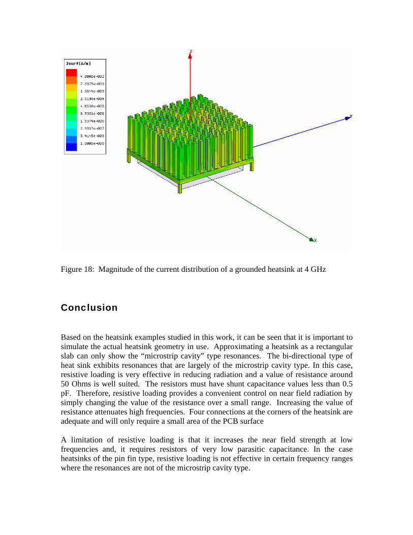
Figure 18: Magnitude of the current distribution of a grounded heatsink at 4 GHz Conclusion Based on the heatsink examples studied in this work, it can be seen that it is important to simulate the actual heatsink geometry in use. Approximating a heatsink as a rectangular slab can only show the “microstrip cavity” type resonances. The bi-directional type of heat sink exhibits resonances that are largely of the microstrip cavity type. In this case, resistive loading is very effective in reducing radiation and a value of resistance around 50 Ohms is well suited. The resistors must have shunt capacitance values less than 0.5 pF. Therefore, resistive loading provides a convenient control on near field radiation by simply changing the value of the resistance over a small range. Increasing the value of resistance attenuates high frequencies. Four connections at the corners of the heatsink are adequate and will only require a small area of the PCB surface A limitation of resistive loading is that it increases the near field strength at low frequencies and, it requires resistors of very low parasitic capacitance. In the case heatsinks of the pin fin type, resistive loading is not effective in certain frequency ranges where the resonances are not of the microstrip cavity type.

References [1] P. Sochoux, J. Yu, A. Bhobe, and F. Centola, “Heat Sink Design Flow for EMC”,
Proceedings DesignCon 2008, Santa Clara, CA, February 4-7, 2008. [2] X. Wu, “Impedance Matched Lossy Decoupling for PCB Power Delivery, and
Heatsink Radiated EMI Noise”, DesignCon 2006, Santa Clara, CA, February 6-9, 2006.
[3] Weimin Shi, V. Adsure, Y. Chen, and H. Kroger, “Improving Signal Integrity in
Circuit Boards by incorporating absorbing materials”, Proceedings ECTC, 2000. [4] Bruce Archambeault, Juan Chen, Satich Pratepeni, Lauren Zhang, and David Wittwer,
“Comparison of Various Numerical Modeling Tools Against a Standard Problem Concerning Heat Sink Emissions - Standard Modeling Paper 3", http://www.ewh.ieee.org/cmte/tc9
[5] Syed A. Bokhari, Istvan Novak, “Effect of Dissipative Edge Terminations on the
Radiation of Power/Ground Planes,” Proceedings of the IEEE EMC Symposium, August 21-25, 2000, Washington, D.C.
[6] http://www.ansoft.com/products/hf/hfss