Embed Size (px)
Citation preview
Control of DC Power Distribution Systems
and Low-Voltage Grid-Interface Converter Design
Fang Chen
Dissertation submitted to the Faculty of the Virginia Polytechnic
Institute and State University in partial fulfillment of the
requirements for the degree of
Doctor of Philosophy
in
Electrical Engineering
Dushan Boroyevich (Co-Chair)
Rolando Burgos (Co-Chair)
Virgilio A. Centeno
William T. Baumann
Alfred L. Wicks
March 22, 2017
Blacksburg, Virginia
Keywords: dc power distribution, microgrid, droop control, load sharing,
grid interface converter, single phase ac-dc
Copyright 2017, Fang Chen

Control of DC Power Distribution Systems
and Low-Voltage Grid-Interface Converter Design
Fang Chen
Abstract
DC power distribution has gained popularity in sustainable buildings, renewable
energy utilization, transportation electrification and high-efficiency data centers. This
dissertation focuses on two aspects of facilitating the application of dc systems: (a) system-
level control to improve load sharing, voltage regulation and efficiency; (b) design of a
high-efficiency interface converter to connect dc microgrids with the existing low-voltage
ac distributions, with a special focus on common-mode (CM) voltage attenuation.
Droop control has been used in dc microgrids to share loads among multiple sources.
However, line resistance and sensor discrepancy deteriorate the performance. The
quantitative relation between the droop voltage range and the load sharing accuracy is
derived to help create droop design guidelines. DC system designers can use the guidelines
to choose the minimum droop voltage range and guarantee that the sharing error is within
a defined range even under the worst cases.
A nonlinear droop method is proposed to improve the performance of droop control.
The droop resistance is a function of the output current and increases when the output
current increases. Experiments demonstrate that the nonlinear droop achieves better load
sharing under heavy load and tighter bus voltage regulation. The control needs only local
information, so the advantages of droop control are preserved. The output impedances of
the droop-controlled power converters are also modeled and measured for the system
stability analysis.
Communication-based control is developed to further improve the performance of dc
microgrids. A generic dc microgrid is modeled and the static power flow is solved. A
secondary control system is presented to achieve the benefits of restored bus voltage,

enhanced load sharing and high system efficiency. The considered method only needs the
information from its adjacent node; hence system expendability is guaranteed.
A high-efficiency two-stage single-phase ac-dc converter is designed to connect a
380 V bipolar dc microgrid with a 240 V split-phase single-phase ac system. The converter
efficiencies using different two-level and three-level topologies with state-of-the-art
semiconductor devices are compared, based on which a two-level interleaved topology
using silicon carbide (SiC) MOSFETs is chosen. The volt-second applied on each inductive
component is analyzed and the interleaving angles are optimized. A 10 kW converter
prototype is built and achieves an efficiency higher than 97% for the first time.
An active CM duty cycle injection method is proposed to control the dc and low-
frequency CM voltage for grounded systems interconnected with power converters.
Experiments with resistive and constant power loads in rectification and regeneration
modes validate the performance and stability of the control method. The dc bus voltages
are rendered symmetric with respect to ground, and the leakage current is reduced. The
control method is generalized to three-phase ac-dc converters for larger power systems.

Control of DC Power Distribution Systems
and Low-Voltage Grid-Interface Converter Design
Fang Chen
General Audience Abstract
DC power distribution gains popularity in sustainable buildings, renewable energy
utilization, transportation electrification and high-efficiency data centers. This dissertation
focuses on two aspects of facilitating the application of dc systems: (a) system-level control
to improve load sharing, voltage regulation and efficiency; (b) a high-efficiency converter
design to connect dc microgrids with the existing low-voltage ac utility, with a special
focus on controlling the dc bus to ground voltage.
An analytical model is established to solve the power flow and voltage distribution in
a generic dc system. The impact from cable resistance and measurement error on droop
control is quantitatively analyzed, based on which droop design guidelines are proposed.
DC system designers can use the conclusion to choose a minimum droop voltage range and
guarantee a predefined load sharing accuracy. A nonlinear droop control method and a
communication-based control method are proposed to further improve the dc system
performance. The benefits include better load sharing, tighter voltage regulation and higher
system efficiency.
To connect dc grids with the low-voltage ac distribution, a high-efficiency bidirectional
ac-dc interface converter is designed and built. Different converter topologies with state-
of-the-art power semiconductor devices are evaluated. Based on the comparison, an
interleaved converter is selected and achieves an efficiency higher than 97% with an
optimized passive component design. This converter is also capable of generating
symmetric dc bus to ground voltages using a dedicated common-mode voltage control
system, and is thus suitable for bipolar dc distribution systems.

v
Dedicated to:
My parents:
Xihuan Chen, Weimin Fang
My grandparents:
Chonghao Chen, Yuxian Zhu
Guoliang Fang, Shumin Li

vi
Acknowledgements
Foremost, I would like to express my sincere gratitude to my advisors Dr. Dushan
Boroyevich and Dr. Rolando Burgos, who provided me with this great opportunity to learn
and research at the Center for Power Electronics Systems (CPES). I am very fortunate to
have both of them as my Ph.D. advisors. Their visions and knowledge guided me on the
path of exploring power electronics. Their encouragement supported me and motivated me
to embrace the continuous challenges. Their humorous attitude towards life and meticulous
attitude towards work showed me a model for being an interesting and responsible person.
These experiences and qualities will be my invaluable assets.
In addition to my advisors, I would like to thank the rest of my committee, Dr. Alfred
L. Wicks, Dr. Virgilio A. Centeno, Dr. William T. Baumann, and Dr. Douglas K. Lindner,
for giving me valuable advice and insightful suggestions from different technical
perspectives. It has been wonderful to have them on my advisory committee.
I wish to thank the CPES director, Dr. Fred C. Lee, for his inspiring guidance and strict
requirements through the Renewable Energy and Nanogrids (REN) min-consortium
weekly meetings. I learned a great deal from him about organizing the logic of my research
and presentations.
My special thanks goes to Dr. Josep M. Guerrero and Dr. Juan Carlos Vasquez for
inviting me to conduct part of my research at Aalborg University, Denmark. I would also
like to thank those who helped me during this study abroad time. This experience in Europe
not only enriched my knowledge but broadened my horizons as well.
I would like to thank the CPES administrative staff members, Ms. Marianne Hawthorne,
Ms. Teresa Shaw, Ms. Trish Rose, Ms. Linda Long, Mr. David Gilham, and Ms. Lauren
Shutt for their support and help during my time at CPES.
I also would like to thank all my fellows at CPES. Their help, mentorship, and
friendship provided a basis for the accomplishment of this work. Although I cannot list all
of them, I would like to take this chance and thank those who made valuable input to my
work. They are Dr. Dong Dong, Dr. Xuning Zhang, Dr. Zhiyu Shen, Dr. Mingkai Mu, Dr.
Marko Jaksic, Dr. Bo Wen, Dr. Lingxiao Xue, Dr. Zheming Zhang, Dr. Daocheng Huang,

vii
Dr. Shuilin Tian, Dr. Yang Jiao, Mr. Igor Cvetkovic, Mr. Wei Zhang, Mr. Jun Wang, Mr.
Qiong Wang, Mr. Chi Li, Mr. Ming Lv, Mr. Zhongsheng Cao, Mr. Xuebing Chen, Ms.
Niloofar Rashidi, Ms. Christina DiMarino, Mr. Yi-Hsun Hsieh, Mr. Alinaghi Marzoughi,
Ms. Bingyao Sun, Mr. Ruiyang Qin, Mr. Shishuo Zhao, Mr. Yadong Lyu, Mr. Sungjae
Ohn, Ms. Ye Tang, Mr. Yue Xu, Ms. Qian Li, and so many others.
With much love and gratitude, I want to thank my parents Xihua Chen and Weimin
Fang, for their endless love, encouragement, and support throughout my life. Thank you
for educating me from a very early age, creating a better environment for my education
and supporting me in pursuing my Ph.D. abroad. I owe you so much and I am so lucky to
be your son!
Finally, I must thank my girlfriend Li Wang, who came to the U.S. with me,
accompanied me and encouraged me. I would not have accomplished this work without
you being here.
I am sure I have missed expressing my appreciation to many people. To you all, thank
you so much!
This work is supported by the Wide Band Gap High-Power Converters & Systems
(WBG-HPCS) mini-consortium (formerly known as Renewable Energy and Nanogrids
(REN) mini-consortium).

Fang Chen Table of Contents
viii
Table of Contents
Chapter 1. Introduction 1
1.1. Research background and motivations 1
1.2. Literature review 6
1.2.1. Power architecture development for dc microgrids 6
1.2.2. Control methods for dc microgrids 9
1.2.3. Low-voltage utility interface converter design for dc microgrids 15
1.3. Challenges and research objectives 20
1.3.1. Challenges in the deployment of dc power distribution 20
1.3.2. Research objectives 23
1.4. Dissertation outline 24
Chapter 2. Design of Droop Control for DC Power Distribution Systems 26
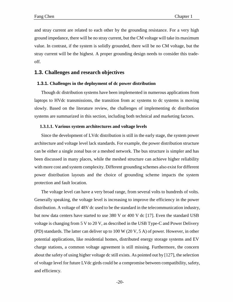
2.1. The benefit and realization of droop control in dc systems 26
2.2. Analysis of factors degrading the performance of droop control 29
2.2.1. The effect of cable resistance 29
2.2.2. The effect of voltage offset 34
2.2.3. Experimental verification 35
2.3. Quantitative analysis for two-source systems 36
2.3.1. Identification of the worst source and load locations 36
2.3.2. Load sharing accuracy as a function of source power ratings 37
2.3.3. Load sharing accuracy as a function of droop voltage range 39
2.4. Generalization to three-source and multi-source multi-load systems 41
2.4.1. Analysis for the side source 41
2.4.2. Analysis for the middle source 43
2.4.3. Generalization to multi-source system 44
2.5. Proposed droop design guidelines for dc systems 45
2.6. Conclusion 46

Fang Chen Table of Contents
ix
Chapter 3. A Nonlinear Droop Control to Improve Load Sharing and Voltage Regulation 48
3.1. Review of techniques to improve the load sharing and voltage regulation of droop control 48
3.2. The proposed nonlinear droop control 50
3.2.1. The principle of the proposed nonlinear droop control 50
3.2.2. Comparison of different nonlinear droop profiles 51
3.2.3. Performance comparison between linear and nonlinear droops 53
3.3. Experimental verification 54
3.3.1. Single-source droop characteristic test 54
3.3.2. Comparison between traditional linear droop and proposed nonlinear droop 55
3.4. Output impedance and stability considerations 62
3.4.1. Review of dc system stability criteria 62
3.4.2. Output impedance small-signal modeling for droop-controlled voltage sources 64
3.4.3. Measurement of the output impedance for power converters 67
3.5. Conclusion 72
Chapter 4. DC System Power Flow Analysis and Performance Improvement Using Nearest-Node
Communication 74
4.1. Review of microgrid control strategies with communication links 74
4.2. Static power flow analysis of a generic dc microgrid 76
4.3. DC system efficiency analysis and optimization 79
4.4. A distributed power flow control strategy using nearest-node communication 84
4.5. Experimental verification 90
4.5.1. Hardware-in-the-loop test bed 90
4.5.2. Validation of the static system model 92
4.5.3. Validation of the distributed power flow control method 95
4.6. Conclusion 97
Chapter 5. A High-Efficiency Transformer-less Single-Phase Utility-Interface Converter for 380 V DC
Microgrids 99
5.1. Design application and requirements 99
5.1.1. Gird-interface converter for future residential houses 99
5.1.2. Residential ac and dc grid interfaces 100

Fang Chen Table of Contents
x
5.1.3. Applicable standards 102
5.2. Converter topology selection 103
5.2.1. Two-stage topology to decouple the common-mode voltage 103
5.2.2. Selection of the phase-leg structure to achieve high efficiency 104
5.3. Power stage design 113
5.3.1. Pluggable phase-leg module design 113
5.3.2. Interleaving angle selection and filter design 119
5.4. Control system design 130
5.4.1. Control system for the differential-mode quantities 130
5.4.2. Control system for common-mode voltages 131
5.5. Experimental results 137
5.6. Conclusion 141
Chapter 6. Low-Frequency Common-Mode Voltage Control for Systems Interconnected with Power
Converters 142
6.1. Problems when grounded systems are connected by non-isolated converters 142
6.2. Principle of the active low-frequency common-mode voltage control 145
6.3. Operating range of the common-mode duty cycle injection 147
6.3.1. The impact from dc-link voltage and ac voltage 150
6.3.2. The impact from asymmetric ac grounding 152
6.4. Common-mode circuit small-signal modeling and control loop design 153
6.5. Generalization to three-phase ac interface 157
6.6. Experimental results and impact on ac current 158
6.7. Conclusion 163
Chapter 7. Summary, Conclusions and Future Work 164
7.1. Summary 164
7.2. Conclusions 164
7.3. Future work 165
References 167
Appendix 186

Fang Chen Table of Contents
xi
A.1 MATLAB code to calculate the volt-second on inductors 186
A.2 Circuit schematic of the pluggable phase-leg card 189

Fang Chen List of Figures
xii
List of Figures Fig. 1.1. Trend of global renewables installed capacity. 2
Fig. 1.2. Initiative of dc nanogrid for future houses at CPES, Virginia Tech. 5
Fig. 1.4. General LVdc industrial power distribution with UPS features. 6
Fig. 1.5. Single bus dc microgrid with battery directly tied. 7
Fig. 1.6. DC microgrid with power management. 8
Fig. 1.7. Bipolar dc bus with voltage balancer. 8
Fig. 1.8. Control structures for dc microgrid. 10
Fig. 1.9. Principle of the dc bus signaling. 12
Fig. 1.11. Definitions of DM and CM signals in coupled pair transmission lines [108]. 17
Fig. 1.12. The CM path in PV applications [110]. 18
Fig. 1.13. CM and DM current paths in motor drive applications [114]. 18
Fig. 2.1. Droop control in ac and dc grids. 27
Fig. 2.2. Droop control in a two-source one-load dc system. 28
Fig. 2.3. A control structure to realize virtual droop resistance. 29
Fig. 2.4. Impact of line resistance on voltage distribution. 30
Fig. 2.5. Two sources droop with cable resistances. 31
Fig. 2.6. System to analyze the effect of line resistance. 32
Fig. 2.7. Load sharing and voltage regulation comparison with different droop resistances. 33
Fig. 2.8. Trade-off between voltage regulation and load sharing when choosing a droop resistance. 34
Fig. 2.9. Impact of voltage offset on load sharing. 35
Fig. 2.10. Load sharing experiment with line resistance and measurement error. 36
Fig. 2.11. The worst source and load locations for two-source systems. 37
Fig. 2.12. Sharing error as a function of source ratings. 38
Fig. 2.13. Sharing error as a function of droop voltage range. 40
Fig. 2.14. Quantitative relation between droop voltage range and load sharing accuracy. 40
Fig. 2.15. A three-source multi-load system. 41
Fig. 2.16. Two extreme cases for side Source 1. 42
Fig. 2.17. Source placement and combination for the most current sharing from Source 1. 43
Fig. 2.18. Two worst cases for the middle source. 43
Fig. 2.19. The worst source and cable placement for the middle source to take the least load. 44
Fig. 2.20. A multi-source multi-load system and its worst case. 45
Fig. 3.1. Diagram of the proposed nonlinear droop control. 51
Fig. 3.2. Different droop curves and corresponding droop resistances. 52
Fig. 3.3. Two-source paralleling test with inserted cable. 54
Fig. 3.4. Simulation comparison between the traditional and proposed droop methods. 54
Fig. 3.5. Single-source droop characteristic test. 55

Fang Chen List of Figures
xiii
Fig. 3.6. Linear droop with negligible cable resistance. 56
Fig. 3.7. Nonlinear droop with negligible cable resistance. 56
Fig. 3.8. Linear droop (Rd = 1 Ω) with 0.2 Ω cable resistance. 57
Fig. 3.9. Linear droop (Rd = 0.5 Ω) with 0.2 Ω cable resistance. 57
Fig. 3.10. The linear droop (Rd = 1 Ω) with 0.2 Ω cable resistance. 58
Fig. 3.11. The inverse parabola droop with 0.2 Ω cable resistance. 58
Fig. 3.12. A three-source dc system with tie-line resistance and measurement error. 59
Fig. 3.13. Segments to compare different droop profiles. 60
Fig. 3.14. Droop comparison in Segment 1. 61
Fig. 3.15. Droop comparison in Segment 2. 61
Fig. 3.16. Droop comparison in Segment 3. 61
Fig. 3.17. Droop comparison in Segment 4. 61
Fig. 3.18. Droop comparison in Segment 5. 61
Fig. 3.19. Load step test for different droop profiles. 62
Fig. 3.20. A zonal dc bus system with distributed sources and loads. 63
Fig. 3.21. Bode plot of the GMPM criterion. 64
Fig. 3.22. Nyquist plot of the GMPM criterion. 64
Fig. 3.23. Buck converter with droop control loop. 65
Fig. 3.24. Control diagram of a droop-controlled voltage source converter. 65
Fig. 3.25. Converter output impedance measurement circuit. 68
Fig. 3.26. The modeled and measured output impedance without droop control. 69
Fig. 3.27. Modeled and measured output impedance with linear droop control. 69
Fig. 3.28. Output impedance of the ellipse droop under light load. 70
Fig. 3.29. Output impedance of the ellipse droop under medium load. 70
Fig. 3.30. Output impedance of the ellipse droop under heavy load. 71
Fig. 3.31. Output impedance comparison between linear and ellipse droop. 72
Fig. 4.1. A generic dc microgrid. 76
Fig. 4.2. A two-source one-load system with negligible cable resistance. 80
Fig. 4.3. A typical power converter efficiency curve. 80
Fig. 4.4. Two-source paralleling efficiency. 81
Fig. 4.5. Source current distribution for higher and lower system efficiency limits. 82
Fig. 4.6. A two-source system with cable resistance. 82
Fig. 4.7. Two-source paralleling efficiency with cable losses. 83
Fig. 4.8. Source current distribution with cable losses. 83
Fig. 4.9. The system efficiency with no droop and strong droop. 84
Fig. 4.10. The system structure with nearest-node communication. 86
Fig. 4.11. Bus voltage restoration module. 87

Fang Chen List of Figures
xiv
Fig. 4.12. Load sharing enhancement module (proportional to source ratings). 87
Fig. 4.13. Tie-line current control module. 88
Fig. 4.14. The proposed power flow controller. 88
Fig. 4.15. The evaluated three-source three-load dc distribution system. 89
Fig. 4.16. Voltage and current without secondary control. 90
Fig. 4.17. Voltage and current with voltage restoration. 90
Fig. 4.18. Voltage and current with voltage restoration and current sharing control. 90
Fig. 4.19. Voltage and current with voltage restoration and tie-line current control. 90
Fig. 4.20. Experimental setup. 91
Fig. 4.21. The designed graphical user interface (GUI). 92
Fig. 4.22. Bus voltage and source current with tie-line resistances. 93
Fig. 4.23. Bus voltage and source current with drifted voltage set points. 94
Fig. 4.24. Bus voltage and source current with different droop resistances. 95
Fig. 4.25. Experimental waveforms with voltage restoration. 96
Fig. 4.26. Experimental waveforms with current balancing control. 96
Fig. 4.27. Experimental waveforms with both voltage restoration and current balancing. 97
Fig. 4.28. Experimental waveforms with direct tie-line current control. 97
Fig. 5.1. DC power distribution in a future home. 100
Fig. 5.2. Different residential ac distribution interfaces: (a) split-phase single-phase system; (b) asymmetric
single-phase system; (c) three-phase system. 101
Fig. 5.3. Configurations of dc power distribution systems: (a) unipolar; (b) bipolar. 101
Fig. 5.4. DC side droop characteristic of the ECC converter. 102
Fig. 5.5. Two-stage bidirectional single-phase ac-dc converter with common-mode decoupling. 103
Fig. 5.6. Evaluated bidirectional ac-dc topologies: (a) 2L full-bridge; (b) 2L full-bridge with paralleled
MOSFETs; (c) 3L diode clamped; (d) 3L T-type. 105
Fig. 5.7. 2L and 3L full-bridge output voltages comparison. 106
Fig. 5.8. Different phase-leg structures with selected devices. 107
Fig. 5.9. Pictures of the Si and SiC power devices. 108
Fig. 5.10. Comparison between 1200V IGBT (MITSUBISHI PM75CL1A120) and 1200V SiC MOSFET
(CREE C2M0025120D): (a) output characteristic; (b) switching energy. 109
Fig. 5.11. Efficiency comparison for different 2L and 3L topologies. 110
Fig. 5.12. The required boost inductance with different switching frequencies. 110
Fig. 5.13. Loss breakdown for different topologies and devices: (a) fsw = 20 kHz; (b) fsw = 40 kHz. 111
Fig. 5.14. The impact of device paralleling on converter efficiency. 112
Fig. 5.15. The impact of switching frequency on loss distribution. 113
Fig. 5.16. Structure of a single phase-leg card. 114
Fig. 5.17. A pluggable 5 kW phase-leg card. 115

Fang Chen List of Figures
xv
Fig. 5.18. Phase-leg double pulse test waveforms. 116
Fig. 5.19. MOSFET turn-on waveforms. 116
Fig. 5.20. MOSFET turn-off waveforms. 117
Fig. 5.21. Waveforms for switching loss calculation. 118
Fig. 5.22. Desaturation/over-current protection test. 119
Fig. 5.23. Circuit to derive the design constraints for each component. 120
Fig. 5.24. Inductor voltage analysis: step 1. 122
Fig. 5.25. Inductor voltage analysis: step 2. 123
Fig. 5.26. Inductor voltage analysis: step 3. 123
Fig. 5.27. Driving signals without phase shift. 125
Fig. 5.28. Driving signals with phase shift. 126
Fig. 5.29. Volt-second with different duty cycles. 126
Fig. 5.30. Volt-second on the interphase inductor Linter. 127
Fig. 5.31. Volt-second on the differential-mode inductor LDM. 128
Fig. 5.32. Volt-second on the common-mode choke LCM. 128
Fig. 5.33. Interphase inductor with different winding placements. 129
Fig. 5.34. Picture of the 10 kW two-stage ac-dc power converter. 130
Fig. 5.35. The ac-dc stage controller. 131
Fig. 5.36. The dc-dc stage controller. 131
Fig. 5.37. Common-mode equivalent circuit. 132
Fig. 5.38. Simplified CM circuit for CM controller design. 133
Fig. 5.39. Final CM circuit with CM control loop. 133
Fig. 5.40. Modeled and simulated CM transfer functions. 134
Fig. 5.41. The simulated dc bus to ground voltage. 135
Fig. 5.42. Complete circuit schematic and control system. 136
Fig. 5.43. Rectifier mode ac voltage and current, dc-link voltage and dc bus voltage. 137
Fig. 5.44. Symmetric dc bus to ground voltages. 137
Fig. 5.45. Unity power factor operation and ground leakage current. 138
Fig. 5.46. Converter efficiency with 500 V dc-link voltage. 138
Fig. 5.47. Relation between converter efficiency and dc-link voltage. 139
Fig. 5.48. Efficiency with a variable dc-link voltage. 139
Fig. 5.49. Efficiency comparison between ECC Gen 1 and Gen 2. 140
Fig. 5.50. Loss breakdown for ac-dc and dc-dc stages. 141
Fig. 6.1. AC power distribution layouts in North America and Europe. 143
Fig. 6.2. DC power distribution system using TN grounding scheme. 144
Fig. 6.3. Common-mode current circulating between interconnected ac and dc systems. 144
Fig. 6.4. The converter topology and CM voltage control loop. 145

Fang Chen List of Figures
xvi
Fig. 6.5. DC bus to ground voltages are asymmetric and have ripples. 146
Fig. 6.6. Derivation of low-frequency CM circuit for operating range discussion. 148
Fig. 6.7. Impact from the dc-link voltage on the CM control margin. 151
Fig. 6.8. Impact from the ac voltage on the CM control margin. 151
Fig. 6.9. DC bus voltage before and after CM control with symmetric ac. 152
Fig. 6.10. Total and injected duty cycle with symmetric ac. 152
Fig. 6.11. DC bus voltages before and after CM control with asymmetric ac. 153
Fig. 6.12. Total and injected CM duty cycle with asymmetric ac. 153
Fig. 6.13. Complete CM equivalent circuit with floating filter. 154
Fig. 6.14. Power stage transfer function from dCM to vdc-. 156
Fig. 6.15. The CM control loop gain with resonant controller. 156
Fig. 6.16. Two-stage three-phase ac-dc converter with CM voltage control loop. 157
Fig. 6.17. Bidirectional experiment configuration. 159
Fig. 6.18. Start-up of the CM voltage control. 159
Fig. 6.19. Comparison of the steady-state dc bus CM voltage. 160
Fig. 6.20. Comparison of the ac current Iac, floating filter current If and leakage current Ig. 160
Fig. 6.21. Comparison of dc bus voltages during the transition from rectification to regeneration mode. 161
Fig. 6.22. Load step-up test for DM and CM dc bus voltages with the CM control. 162
Fig. 6.23. Duty cycles and ac inductor current waveform before and after applying CM control. 162

Fang Chen List of Tables
xvii
List of Tables Table 1.1. DC system characteristics 3
Table 2.1. Typical cable sizes in residential applications and corresponding voltage drops [139]. 29
Table 3.1. Comparison and evaluation of different droops. 53
Table 4.1. Source voltage, current, and load sharing with tie-line resistances. 93
Table 4.2. Source voltage, current, and load sharing with drifted voltage set points. 94
Table 4.3. Source voltage, current, and load sharing with different droop resistances. 95
Table 5.1. IEEE 1547 and IEEE 519 requirements for harmonic current on ac side. 102
Table 5.2. Current ripple and required inductance for 2-level full-bridge converters. 106
Table 5.3. Evaluated topology and device combinations. 107
Table 5.4. DM and CM filter parameters. 129
Table 5.5. Controller parameters 135
Table 6.1. CM filter parameters 155

Fang Chen Chapter 1
-1-
Chapter 1. INTRODUCTION
This chapter presents the motivations and objectives of this work, along with an
introduction of the background and applications of dc power distribution systems. A review
of state-of-the-art techniques in the dc distribution is provided, with a focus on system-
level control and interconnection with the low-voltage ac grid. The challenges are provided,
followed by the research objectives and dissertation outline.
1.1. Research background and motivations
With the increasing energy consumption and growing population, sustainable energy
supply is a concern for contemporary society. For a very long time, the energy boom was
based on fossil fuels like oil, coal and natural gas. Not only is the supply of these resources
limited, their exploitation and utilization also cause severe environmental problems.
Renewable energy technologies are seen as one of the most important solutions to solve
the energy crisis, and they are being developed to replace or supplement traditional energy
resources. Among different kinds of renewable sources, hydropower, wind, solar, and
bioenergy are the most accessible. Fig. 1.1 lists the growth of the installed capacity of
global renewables from 2007 to 2014 based on data from the Renewable Energy Policy
Network for the 21st Century (REN21) [1]. Historically, hydropower has accounted for
most of the capacity of installed renewables. In recent years, sources like wind and solar
have been catching up. In certain countries, like Denmark, the contribution from
renewables has become more than half of the total electricity generation.
In harvesting renewable energy, both the acquisition and transmission can be in the
form of electricity. The increasing participation of intermittent renewable energy
generation and the rising adoption of distributed generation pose new challenges to the
traditional ac distribution system. Changes are needed to ensure the power system is ready
to cope with the uncertainty of the renewable power generation, and to deal with the
bidirectional power flow from small generation and consumption units at the distribution
level.

Fang Chen Chapter 1
-2-
Fig. 1.1. Trend of global renewables installed capacity.
To satisfy the above requirements, the concept of smart grids has been proposed. A
smart grid provides higher flexibility by incorporating information technology into the
power grid. In this transformation process, nanogrids and microgrids play a crucial role. In
[2], a microgrid is defined as a local cluster of distributed generation (DG) sources, energy
storage, and loads that are integrated together and is capable of operating autonomously. It
allows for local generation and energy storage, which leads to a better match between the
local energy generation and consumption. A robust microgrid should also have “plug-and-
play” operation capability.
DC power distribution is believed to be a promising and simple solution to integrate
distributed generation and energy storage devices as well as manage the power
consumption and utilization among multiples electronic loads, thereby eliminating
redundant components and improving the system efficiency [3]. Compared to its ac
counterpart, stability criteria in the dc system are clearer. The dc-dc power conversion is
simpler and usually more efficient than the ac-dc conversion.
Because of the aforementioned benefits, dc distribution has been adopted in a great
number of existing and emerging applications. Depending on the voltage level, the dc
power distribution can be classified into high, medium and low voltage systems; i.e., HVdc,
MVdc and LVdc systems, respectively. HVdc has been used for over 50 years and the
development of the voltage source converter (VSC) in the last 15 years has allowed multi-
0
200
400
600
800
1000
1200
1400
1600
1800
2007 2008 2009 2010 2011 2012 2013 2014
Global Renewables Installed Capacity (GW)
Geothermal
Bio
Solar PV
Wind
Hydro
Fang Chen Chapter 1
-3-
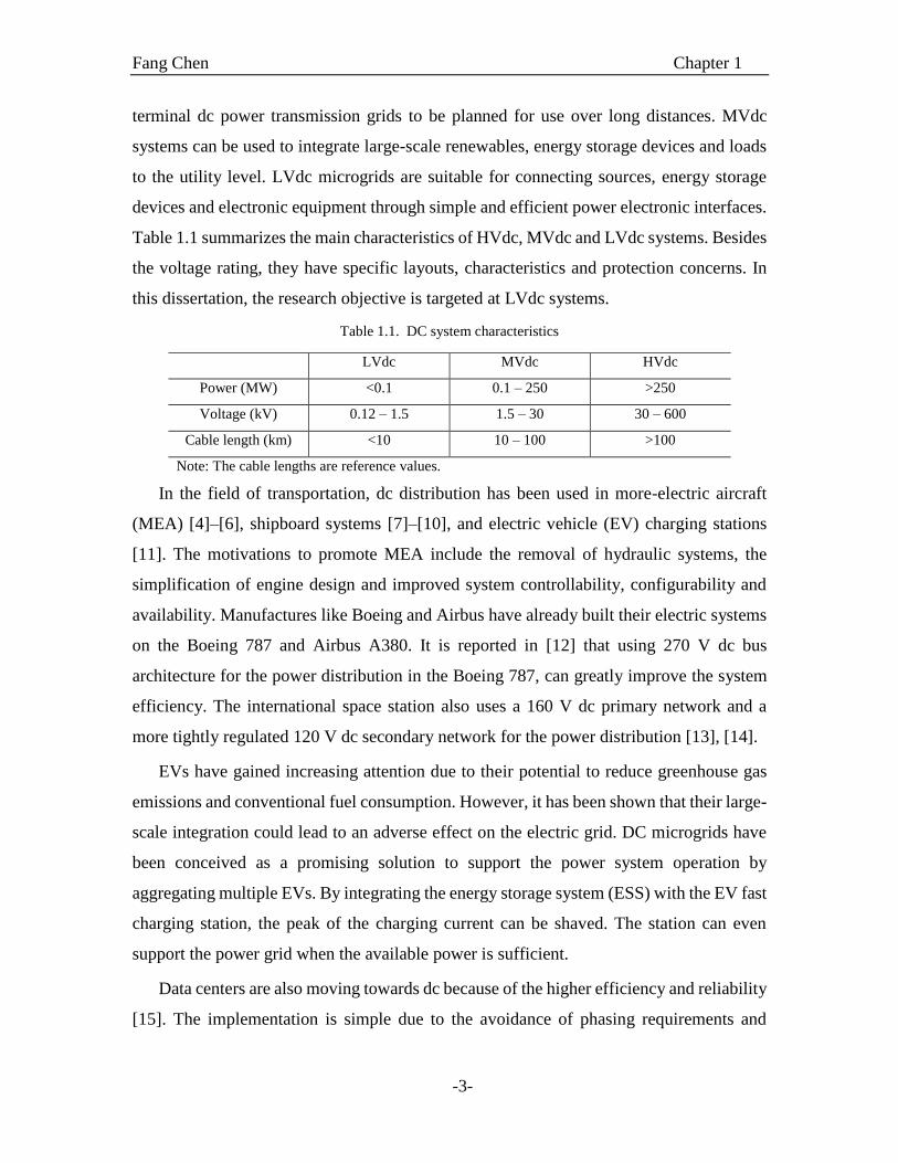
terminal dc power transmission grids to be planned for use over long distances. MVdc
systems can be used to integrate large-scale renewables, energy storage devices and loads
to the utility level. LVdc microgrids are suitable for connecting sources, energy storage
devices and electronic equipment through simple and efficient power electronic interfaces.
Table 1.1 summarizes the main characteristics of HVdc, MVdc and LVdc systems. Besides
the voltage rating, they have specific layouts, characteristics and protection concerns. In
this dissertation, the research objective is targeted at LVdc systems.
Table 1.1. DC system characteristics
LVdc MVdc HVdc
Power (MW) <0.1 0.1 – 250 >250
Voltage (kV) 0.12 – 1.5 1.5 – 30 30 – 600
Cable length (km) <10 10 – 100 >100
Note: The cable lengths are reference values.
In the field of transportation, dc distribution has been used in more-electric aircraft
(MEA) [4]–[6], shipboard systems [7]–[10], and electric vehicle (EV) charging stations
[11]. The motivations to promote MEA include the removal of hydraulic systems, the
simplification of engine design and improved system controllability, configurability and
availability. Manufactures like Boeing and Airbus have already built their electric systems
on the Boeing 787 and Airbus A380. It is reported in [12] that using 270 V dc bus
architecture for the power distribution in the Boeing 787, can greatly improve the system
efficiency. The international space station also uses a 160 V dc primary network and a
more tightly regulated 120 V dc secondary network for the power distribution [13], [14].
EVs have gained increasing attention due to their potential to reduce greenhouse gas
emissions and conventional fuel consumption. However, it has been shown that their large-
scale integration could lead to an adverse effect on the electric grid. DC microgrids have
been conceived as a promising solution to support the power system operation by
aggregating multiple EVs. By integrating the energy storage system (ESS) with the EV fast
charging station, the peak of the charging current can be shaved. The station can even
support the power grid when the available power is sufficient.
Data centers are also moving towards dc because of the higher efficiency and reliability
[15]. The implementation is simple due to the avoidance of phasing requirements and

Fang Chen Chapter 1
-4-
harmonic mitigation. The dc voltage is also changing from 48 V to a higher voltage of
380 V or 400 V [16]. It is reported in [17] that by changing from 480 V ac distribution to
400 V dc, a 7% input power saving is achieved. Companies like ABB and Delta already
have mature products for such applications on the market.
Another important application of the dc distribution is in future residential and
commercial buildings. Because most consumer electronics are intrinsically dc loads, using
a dc power input can save the front-end ac-dc conversion. Furthermore, if renewable
sources and energy storages are integrated, it is possible to achieve the goal of net zero
energy consumption [18]. Several projects in the U.S., Korea, Japan and Denmark are in
progress to demonstrate the benefits of dc distribution and investigate the system
architecture, control and energy management [19]–[29]. In Finland, a ±750 V LVdc
distribution network is being put into use to feed a rural area with a 100 kVA power rating
through a 1.7 km long underground cable [30], [31].
DC distribution is also used for distributed energy storage systems. Small-scale systems
are used for telecommunication facilities [32], while high-power systems appear in
transportation and grid applications [33].
In addition to the aforementioned low-voltage power distribution, dc power is also used
in HVdc applications for long-distance power transmission in projects like connecting off-
shore wind farms and constructing the European supergrid [34].
Because of the broad applications of dc systems, it is very important to solve the
problems in constructing dc microgrids and improving their performance. Companies,
research institutions and universities around the world are working together to promote the
technology development.
The Center for Power Electronics Systems (CPES) at Virginia Tech has built a testbed
for experimental demonstration of LVdc nanogrids for residential buildings [3], [35], [36].
Fig. 1.2 shows the vision of the project to replace the current ac distribution with 380 V dc
in future houses. Different renewable sources, energy storage and electric vehicles are
connected to a dc bus to feed smart loads. By adopting a system-level optimized energy
control, the net energy consumption of the whole house is minimized to achieve the target
of net-zero energy.

Fang Chen Chapter 1
-5-
Utility grid
Plug-in Hybrid
(PHEV)
Solar panels (PV)
Energy Control
Center (ECC)
Wind
Turbine
Energy
StorageAC and Heating
Ventilation…
Smart appliance
Fig. 1.2. Initiative of dc nanogrid for future houses at CPES, Virginia Tech.
The Future Renewable Electric Energy Delivery and Management (FREEDM) system
center at North Carolina State University is working on the concept of an “Energy Internet”,
trying to form a future electric power distribution system that is suitable for the plug-and-
play operation of distributed renewable energy and distributed energy storage devices [37]–
[41].
Furthermore, the Consortium for Electric Reliability Technology Solutions (CERTS),
which consists of several U.S. national laboratories, is working on the CERTS microgrid,
trying to enhance the reliability of the U.S. electric power system and the efficiency of the
competitive electricity market [42].
Outside of the U.S., in Aalborg University at Denmark, an inverter-based Microgrid
Research Laboratory (MGRL) is built to research system integration and hierarchical
control [26], [43], [44]. In Korea, a 380 V testbed is built using isolated power converters.
DC home appliances are modified from conventional ac appliances and included in the
system [45]. In Japan, a three-wire low-voltage bipolar dc microgrid is proposed to supply
super high quality power under various working conditions [46]. The loss of dc distribution
for residential houses is compared with ac systems in [27].
Fang Chen Chapter 1
-6-
There are many other research groups and companies working on dc microgrids, and
not all of their names can be listed. The broad applications and continuous demand to
achieve high-performance dc grids motivate this research.
1.2. Literature review
1.2.1. Power architecture development for dc microgrids
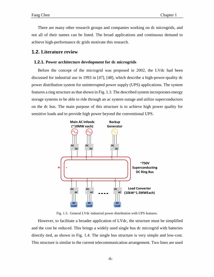
Before the concept of the microgrid was proposed in 2002, the LVdc had been
discussed for industrial use in 1993 in [47], [48], which describe a high-power-quality dc
power distribution system for uninterrupted power supply (UPS) applications. The system
features a ring structure as that shown in Fig. 1.3. The described system incorporates energy
storage systems to be able to ride through an ac system outage and utilize superconductors
on the dc bus. The main purpose of this structure is to achieve high power quality for
sensitive loads and to provide high power beyond the conventional UPS.
ACDC
ACDC
Main AC Infeeds (~10MW each)
ACDC
Backup Generator
DCAC
ACLoad
DCAC
ACLoad
DCAC
ACLoad
Load Converter(10kW~1.5MWEach)
~750V Superconducting
DC Ring Bus+ -
Fig. 1.3. General LVdc industrial power distribution with UPS features.
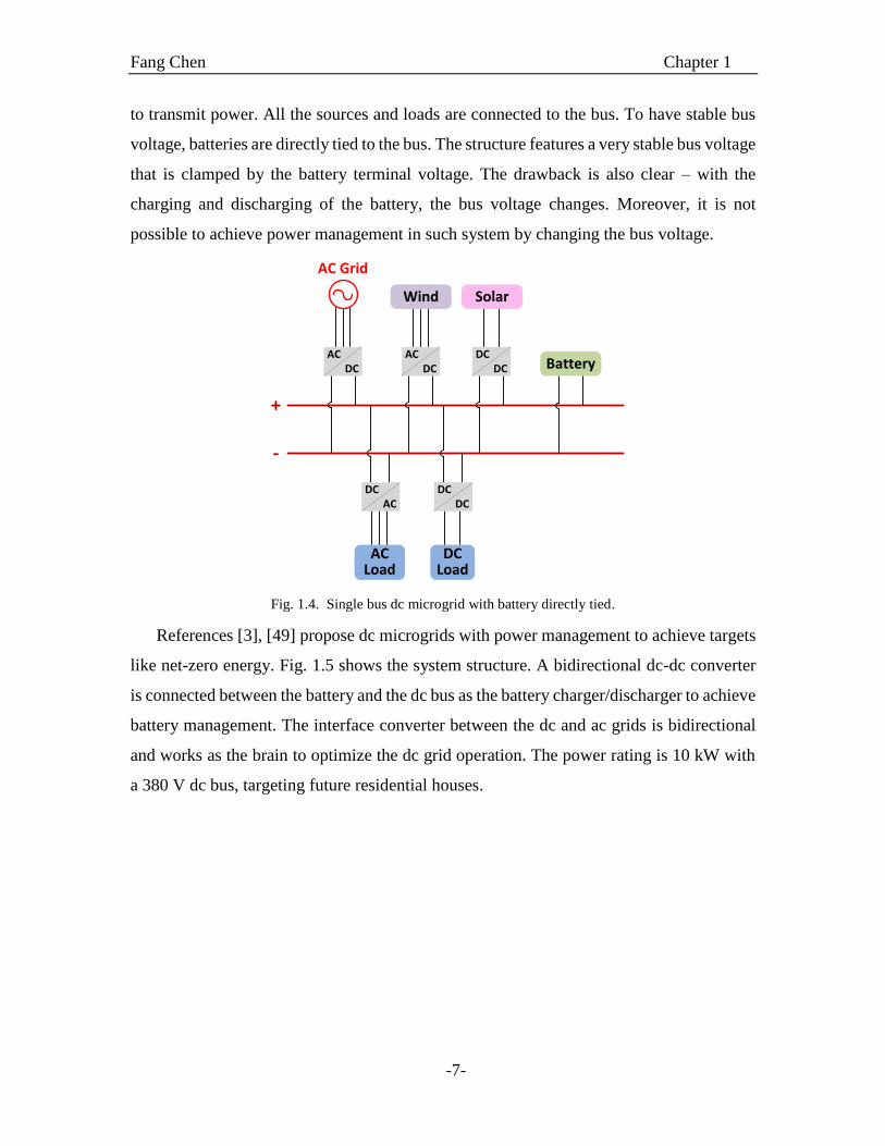
However, to facilitate a broader application of LVdc, the structure must be simplified
and the cost be reduced. This brings a widely used single bus dc microgrid with batteries
directly tied, as shown in Fig. 1.4. The single bus structure is very simple and low-cost.
This structure is similar to the current telecommunication arrangement. Two lines are used
Fang Chen Chapter 1
-7-
to transmit power. All the sources and loads are connected to the bus. To have stable bus
voltage, batteries are directly tied to the bus. The structure features a very stable bus voltage
that is clamped by the battery terminal voltage. The drawback is also clear – with the
charging and discharging of the battery, the bus voltage changes. Moreover, it is not
possible to achieve power management in such system by changing the bus voltage.
ACDC
ACDC
Wind
DCDC
Solar
Battery
AC Grid
DCAC
ACLoad
DCDC
DCLoad
+
-
Fig. 1.4. Single bus dc microgrid with battery directly tied.
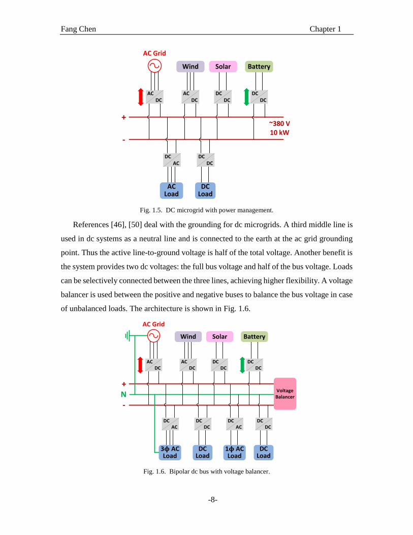
References [3], [49] propose dc microgrids with power management to achieve targets
like net-zero energy. Fig. 1.5 shows the system structure. A bidirectional dc-dc converter
is connected between the battery and the dc bus as the battery charger/discharger to achieve
battery management. The interface converter between the dc and ac grids is bidirectional
and works as the brain to optimize the dc grid operation. The power rating is 10 kW with
a 380 V dc bus, targeting future residential houses.
Fang Chen Chapter 1
-8-
ACDC
ACDC
Wind
DCDC
Solar
AC Grid
DCAC
ACLoad
DCDC
DCLoad
+
-
DCDC
Battery
~380 V 10 kW
Fig. 1.5. DC microgrid with power management.
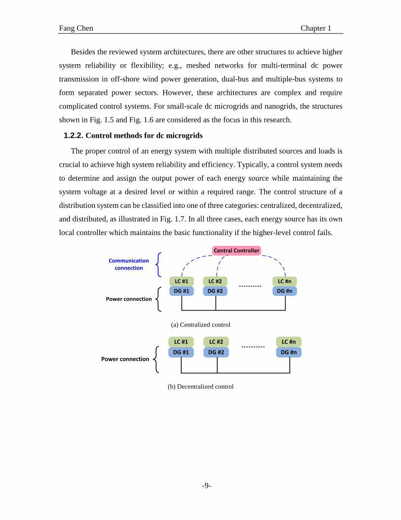
References [46], [50] deal with the grounding for dc microgrids. A third middle line is
used in dc systems as a neutral line and is connected to the earth at the ac grid grounding
point. Thus the active line-to-ground voltage is half of the total voltage. Another benefit is
the system provides two dc voltages: the full bus voltage and half of the bus voltage. Loads
can be selectively connected between the three lines, achieving higher flexibility. A voltage
balancer is used between the positive and negative buses to balance the bus voltage in case
of unbalanced loads. The architecture is shown in Fig. 1.6.
ACDC
ACDC
Wind
DCDC
Solar
AC Grid
DCAC
3ϕ ACLoad
DCDC
DCLoad
+
-
DCDC
Battery
N
DCDC
DCLoad
DCAC
1ϕ ACLoad
VoltageBalancer
Fig. 1.6. Bipolar dc bus with voltage balancer.
Fang Chen Chapter 1
-9-
Besides the reviewed system architectures, there are other structures to achieve higher
system reliability or flexibility; e.g., meshed networks for multi-terminal dc power
transmission in off-shore wind power generation, dual-bus and multiple-bus systems to
form separated power sectors. However, these architectures are complex and require
complicated control systems. For small-scale dc microgrids and nanogrids, the structures
shown in Fig. 1.5 and Fig. 1.6 are considered as the focus in this research.
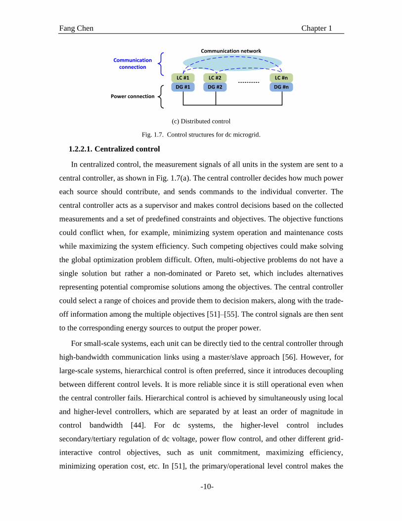
1.2.2. Control methods for dc microgrids
The proper control of an energy system with multiple distributed sources and loads is
crucial to achieve high system reliability and efficiency. Typically, a control system needs
to determine and assign the output power of each energy source while maintaining the
system voltage at a desired level or within a required range. The control structure of a
distribution system can be classified into one of three categories: centralized, decentralized,
and distributed, as illustrated in Fig. 1.7. In all three cases, each energy source has its own
local controller which maintains the basic functionality if the higher-level control fails.
LC #1
DG #1
LC #2
DG #2
LC #n
DG #n
Central Controller
Power connection
Communication connection
(a) Centralized control
LC #1
DG #1
LC #2
DG #2
LC #n
DG #nPower connection
(b) Decentralized control
Fang Chen Chapter 1
-10-
LC #1
DG #1
LC #2
DG #2
LC #n
DG #n
Communication network
Power connection
Communication connection
(c) Distributed control
Fig. 1.7. Control structures for dc microgrid.
1.2.2.1. Centralized control
In centralized control, the measurement signals of all units in the system are sent to a
central controller, as shown in Fig. 1.7(a). The central controller decides how much power
each source should contribute, and sends commands to the individual converter. The
central controller acts as a supervisor and makes control decisions based on the collected
measurements and a set of predefined constraints and objectives. The objective functions
could conflict when, for example, minimizing system operation and maintenance costs
while maximizing the system efficiency. Such competing objectives could make solving
the global optimization problem difficult. Often, multi-objective problems do not have a
single solution but rather a non-dominated or Pareto set, which includes alternatives
representing potential compromise solutions among the objectives. The central controller
could select a range of choices and provide them to decision makers, along with the trade-
off information among the multiple objectives [51]–[55]. The control signals are then sent
to the corresponding energy sources to output the proper power.
For small-scale systems, each unit can be directly tied to the central controller through
high-bandwidth communication links using a master/slave approach [56]. However, for
large-scale systems, hierarchical control is often preferred, since it introduces decoupling
between different control levels. It is more reliable since it is still operational even when
the central controller fails. Hierarchical control is achieved by simultaneously using local
and higher-level controllers, which are separated by at least an order of magnitude in
control bandwidth [44]. For dc systems, the higher-level control includes
secondary/tertiary regulation of dc voltage, power flow control, and other different grid-
interactive control objectives, such as unit commitment, maximizing efficiency,
minimizing operation cost, etc. In [51], the primary/operational level control makes the

Fang Chen Chapter 1
-11-
basic decision related to real-time operation within a millisecond range; the secondary
control, also called the tactical level control makes operational decisions for a group of
local control units in the range of seconds to minutes. The tertiary/strategic level deals with
the overall operation of the system, e.g., startup, shutdown, and power exchange with other
dc grids [57].
In [58], a three-level control structure is discussed. The primary droop control is used
to ensure reliable operation even when communication fails. The secondary and tertiary
control use gossip-based communication to optimize power quality and economic
operation respectively. Reference [59] uses hierarchical control to optimize economics and
the resilient operation. The results are compared with the ac counterpart by simulation.
References [60], [61] research how to use supervisory control to balance and manage the
energy storage within a microgrid. References [62], [63] look at the implementation of
hierarchical control in dc grids and interaction between different levels.
The advantage of this control structure is that the central energy management system
can achieve global optimization based on the acquired global information. However, the
scheme suffers from a heavy computation burden and is subject to a single point of failure.
For mission-critical applications, redundant communication can be installed to reduce the
possibility of failure, but this requires a higher cost.
1.2.2.2. Decentralized control
Decentralized control is achieved exclusively by local controllers. There are a few
methods to achieve this control without any dedicated communication. The most popular
solutions are dc bus signaling (DBS) and power line communication (PLC). It is worth
noting that though the PLC uses the power line as the medium to exchange information
between converters, it is still classified as a type of decentralized control since no extra
physical communication links are added.
The concept of DBS was proposed in [64], [65] in 2004, and then developed and
demonstrated in [35], [66]–[68]. The DBS principle is shown in Fig. 1.8, where a renewable
source and a non-renewable source are connect to the same dc bus. Both the sources have
droop output characteristics, but with different voltage set points. The voltage set point for
the renewable source is V1, and is higher than the non-renewable source set point V2. When
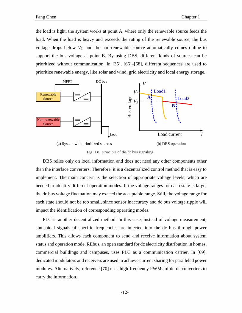
Fang Chen Chapter 1
-12-
the load is light, the system works at point A, where only the renewable source feeds the
load. When the load is heavy and exceeds the rating of the renewable source, the bus
voltage drops below V2, and the non-renewable source automatically comes online to
support the bus voltage at point B. By using DBS, different kinds of sources can be
prioritized without communication. In [35], [66]–[68], different sequences are used to
prioritize renewable energy, like solar and wind, grid electricity and local energy storage.
Renewable
Source
Non-renewable
Source
Load
MPPT DC bus
Bus
volt
age
Load current
V
I
Load1
Load2
V1
V2
A
B
(a) System with prioritized sources (b) DBS operation
Fig. 1.8. Principle of the dc bus signaling.
DBS relies only on local information and does not need any other components other
than the interface converters. Therefore, it is a decentralized control method that is easy to
implement. The main concern is the selection of appropriate voltage levels, which are
needed to identify different operation modes. If the voltage ranges for each state is large,
the dc bus voltage fluctuation may exceed the acceptable range. Still, the voltage range for
each state should not be too small, since sensor inaccuracy and dc bus voltage ripple will
impact the identification of corresponding operating modes.
PLC is another decentralized method. In this case, instead of voltage measurement,
sinusoidal signals of specific frequencies are injected into the dc bus through power
amplifiers. This allows each component to send and receive information about system
status and operation mode. REbus, an open standard for dc electricity distribution in homes,
commercial buildings and campuses, uses PLC as a communication carrier. In [69],
dedicated modulators and receivers are used to achieve current sharing for paralleled power
modules. Alternatively, reference [70] uses high-frequency PWMs of dc-dc converters to
carry the information.
Fang Chen Chapter 1
-13-
In general, PLC is more complex to implement than DBS. Moreover, it is commonly
used only for exchanging operating modes or shutting down the corrupted components in
the system. However, as opposed to the large dc voltage deviation in the DBS, PLC only
periodically injects high-frequency signals. In this sense, the quality of the bus voltage can
be considered to be better.
While the decentralized control is simple and independent of communication, it
inherently has limitations in achieving global performance optimization due to the lack of
information from other units. Moreover, as these methods are solely based on the
interpretation of the local bus voltage or frequency measurement, the accuracy of the
sensors impact the control performance and reliability.
1.2.2.3. Distributed control
Distributed control indicates a control structure in which distributed local controllers
work individually but exchange information through a communication network to optimize
the global performance. In such a configuration, there is no central controller. The main
advantage of this method is that the system can maintain almost full functionality even if
some of the communication links fail. Therefore, the distributed control is immune to a
single point of failure. The computational burden of global optimization is also reduced by
distributing the algorithm to local controllers. Compared with the decentralized control,
distributed control can achieve better overall performance.
Unlike the multi-level communication and control structure in hierarchical control, the
communication network for distributed control is flat and spans over the local controllers.
The design of such a communication network can be complex and requires knowledge of
fields like graph theory. In particular, information exchange can only happen between two
connected nodes and can only contain local information. In other words, if two units are
not connected by a communication link, they will not have access to each other’s data, and
thus their estimation of the whole system could be limited.
The simplest distributed communication network is using a communication bus to
connect all the local controllers. Through this common link, every local controller has
access to all the other nodes without a central controller, thus several improvements can be
achieved. Current sharing and voltage restoration are the most important targets. In [71],
Fang Chen Chapter 1
-14-
voltage deviation and current unbalance are identified when the distance between sources
is large. It uses a low-bandwidth digital communication link to calculate the average of the
total current supplied by the sources, then this value is used to calculate the compensation
needed for the voltage set point. The adjustment is then added to every local controller
through an added control loop. As a result, the bus voltage is restored to the nominal value.
In [72], the impact from communication delay is discussed. It is demonstrated that even
with a 20 ms delay, the stability of the control system can still be guaranteed. In [73], a bi-
proper anti-wind-up design and a pilot bus are added to improve the response during load
switching. A system model is built to determine how the controller parameters and droop
gains affect the system damping performance. In [74], a voltage shifting equalizer is
employed to ensure the converters shift by the same amount of voltage during the
restoration of the dc bus voltage.
A promising approach for distributed control is the multi-agent system (MAS). The
MAS has been discussed for power system integration, restoration, reconfiguration and
power management of microgrids [75]–[77]. The MAS can be considered as a couple of
intelligent hardware and software agents that work together to achieve a global objective.
Recently, the concept of a consensus algorithm is introduced to the area of microgrids
[78]–[81]. The algorithm originated from the area of MAS with an emphasis on the role of
directed information flow, robustness in response to changes in network topology due to
line/node failure, time-delays, and performance guarantees. It is proved that, if the
communication network is connected, all variable values will converge to a common
average after a certain amount of time [82], [83]. In the microgrid application, the
consensus algorithm is embedded within every local controller, which continuously adds
up all algebraic differences of certain variables between itself and adjacent nodes. As a
result, every node can estimate the global bus voltage with its limited information and
restore the bus voltage.
In summary, it can be concluded that distributed control can achieve information
awareness comparable to centralized control. Therefore, objectives such as output current
sharing, voltage restoration, global efficiency improvement, and battery state-of-charge
balancing can be achieved. In this sense, distributed control offers much wider
functionalities than the decentralized control, and avoids the single point of failure. The

Fang Chen Chapter 1
-15-
challenge of this approach is the complexity of analyzing the convergence speed and
stability of the communication network, especially in non-ideal environments that include
communication delay and measurement errors [84].
1.2.3. Low-voltage utility interface converter design for dc microgrids
The utility-interface converter is one of the key components in dc systems. Depending
on the power flow capability, utility-interface converters can be categorized into
unidirectional and bidirectional types. There are many publications on power converter
topologies in PV systems, wind systems and power factor correction (PFC) applications.
Hundreds of topologies exist for ac-dc or dc-ac conversion. However, most of them are not
suitable for bidirectional operation and cannot be used to connect two power distribution
systems.
Single-phase inverters are broadly used in PV applications. References [85], [86]
summarize the popular topologies. Topologies such as the dual-bridge with resonant tank
[87] and dual-bridge without resonant tank [88] have been proposed for isolated topologies.
However, compared with non-isolated topologies, isolated topologies need transformers
and higher numbers of power devices, resulting in lower system efficiency and reliability.
Therefore, transformerless topologies have become more attractive for high-efficiency
applications like bus-interface power converters [89], [90]. Soft-switching techniques have
been studied in grid-tied inverter applications [91], but they suffer the additional cost and
the limit of unidirectional operation.
1.2.3.1. Obstacles to achieve high-efficiency high-density converter design
In single-phase applications, bulky dc-link capacitors pose a major problem, leading to
higher cost and lower power density. Many papers have proposed different solutions to
enable the use of smaller capacitors, such as using an active filter on the ac or the dc side,
multi-stage converters, and bus-conditioning. The development of active energy storage
and the existing techniques are reviewed in this section.
In 1991 and 1992, [92], [93] discusses using an active filter to compensate the
harmonics and eliminate the electrolytic capacitor in three-phase motor applications. In
1997, [94] proposes adding a third phase leg in single-phase applications to reduce the low-
frequency battery ripple current on the dc side. In LED and solar applications, it is reported
Fang Chen Chapter 1
-16-
that by using the auxiliary circuit, a hundred-year life-time can be achieved [95]. In [96],
[97], the capacitor reduction methods for single-phase rectifiers are systematically studied.
The minimum storage requirement is derived independent of topology, then a bidirectional
buck-boost converter is paralleled to the dc bus as the ripple port [98]. In contrast with
paralleling an active ripple port, a series voltage compensator for reduction of the dc-link
capacitor is proposed in [99]. It breaks the dc link and puts a controlled voltage source in
series. The benefit is that the voltage stress for the auxiliary circuit is lower. In [100], a
coupled inductor is used as a basic building block to reduce the ripple. In [101], a review
of different decoupling capacitor locations in PV system is given. The PV-side decoupling,
dc-link decoupling and ac-side decoupling are compared in respect to the capacitor size,
efficiency and control complexity. In [102], a symmetric half-bridge circuit is proposed. In
this configuration, the ripple power circulates between two capacitors in series, which
maintains the total voltage unchanged while buffering the ripple energy. In [103], a
differential ac-dc rectifier is used to reduce the output capacitor with relatively small
changes to the original circuit, but the control is complicated. In [104], [105], a two-stage
structure is used. By allowing a large voltage ripple on the dc-link, the capacitor is reduced.
The drawback is the higher voltage stress.
To summarize, the methods above reduce the required capacitance, but efficiency is
sacrificed because of the extra power processing. However, for the bus-interface converter,
high efficiency is a critical feature and needs to be achieved.
1.2.3.2. Necessity for leakage/common-mode (CM) current reduction
Before discussing the origin and impact of leakage/CM current, the definitions of
differential-mode (DM) and CM quantities are introduced. These terminologies appeared
initially in signal processing using amplifiers [106] and are later used to analyze the
microwave transmission in communication systems [107]. In the latter case, the purpose is
to simplify the analysis of the mixed-mode waves on the coupled transmission lines. As
shown in Fig. 1.9, a general asymmetric coupled transmission line pair over a ground plane
is presented, with pertinent voltages and currents denoted.

Fang Chen Chapter 1
-17-
Fig. 1.9. Definitions of DM and CM signals in coupled pair transmission lines [107].
The DM and CM voltages and currents are defined to construct a self-consistent set of
mixed-mode signals. The DM voltage is defined as
1 2DMv v v (1)
This definition establishes a signal that is no longer referenced to ground. In a
differential circuit, the current that enters the positive input terminal is always equal to the
current that leaves the negative input terminal. The DM current is defined as one-half the
difference between i1 and i2.
1 2
1
2DMi i i (2)
The CM voltage is defined as the average voltage at a port with respect to the ground.
1 2
1
2CMv v v (3)
The CM current at a port is the total current flowing into the port. Therefore, the CM
current is defined as the sum of i1 and i2.
1 2CMi i i (4)
The return current for the CM signal flows through the ground plane.
In the field of power electronics, CM issues have been discussed at length for
photovoltaic (PV) and motor drive applications [108]–[115]. In PV applications, dc-ac
inverters are used to send the harvested energy to the ac grid, as depicted in Fig. 1.10. The
stray capacitance between the PV array and the ground is large. As a result, the CM current
is pronounced. The allowed maximum leakage current is restricted by safety standards
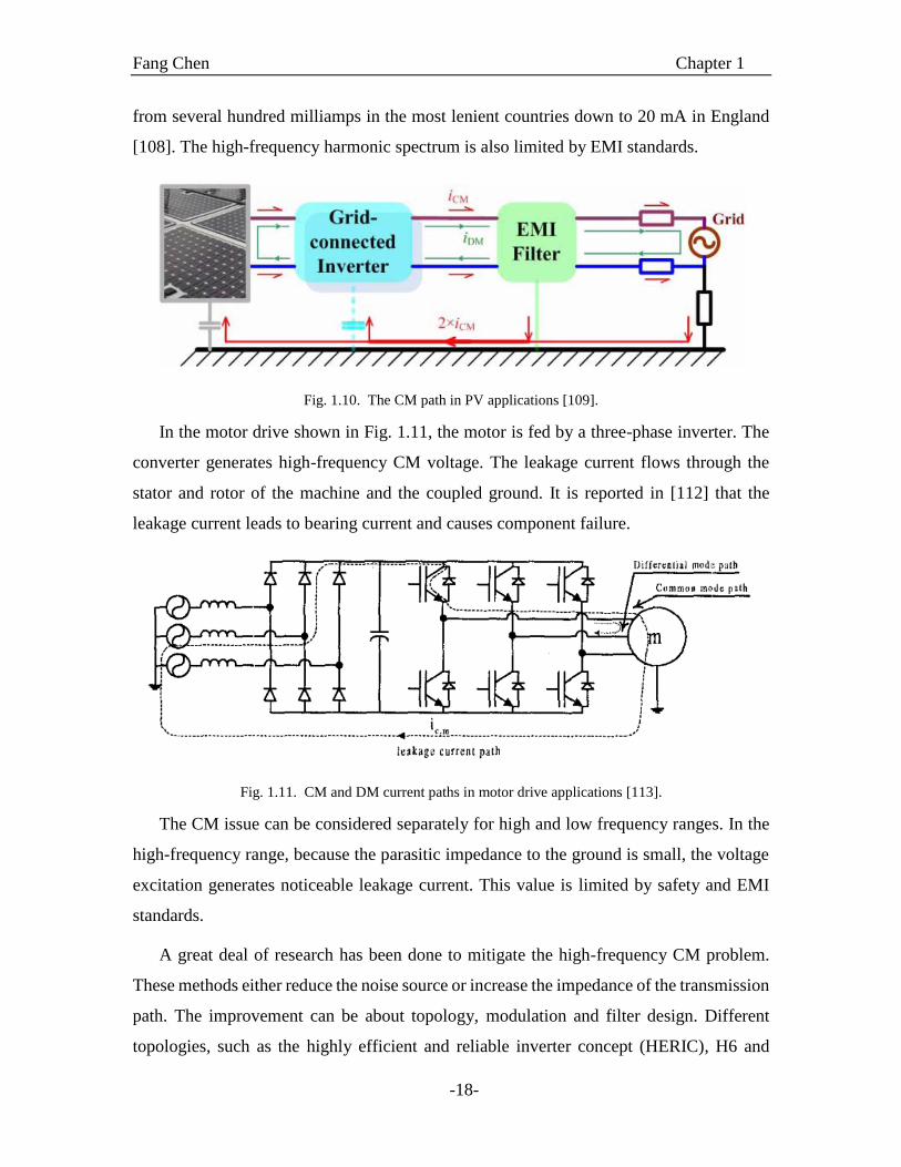
Fang Chen Chapter 1
-18-
from several hundred milliamps in the most lenient countries down to 20 mA in England
[108]. The high-frequency harmonic spectrum is also limited by EMI standards.
Fig. 1.10. The CM path in PV applications [109].
In the motor drive shown in Fig. 1.11, the motor is fed by a three-phase inverter. The
converter generates high-frequency CM voltage. The leakage current flows through the
stator and rotor of the machine and the coupled ground. It is reported in [112] that the
leakage current leads to bearing current and causes component failure.
Fig. 1.11. CM and DM current paths in motor drive applications [113].
The CM issue can be considered separately for high and low frequency ranges. In the
high-frequency range, because the parasitic impedance to the ground is small, the voltage
excitation generates noticeable leakage current. This value is limited by safety and EMI
standards.
A great deal of research has been done to mitigate the high-frequency CM problem.
These methods either reduce the noise source or increase the impedance of the transmission
path. The improvement can be about topology, modulation and filter design. Different
topologies, such as the highly efficient and reliable inverter concept (HERIC), H6 and

Fang Chen Chapter 1
-19-
neutral-point-clamped (NPC) inverter, have been invented or applied to reduce the CM
noise generation in PV applications [116]. In [117], an active CM filter circuit is added to
the main circuit to reduce the ground leakage current. In [118]–[120], different modulation
schemes are proposed to reduce the CM noise by using improved modulation strategies
and limiting the variations of the CM voltage. The closed-loop gate voltage control has
also been used to control the switching speed and limit the EMI [121], [122].
Changing the CM transmission path is another way to limit the noise spectrum. The
traditional filter tries to increase the path impedance so the measured output noise is
reduced. On the other hand, [114], [115] propose using a floating filter in motor drive
applications, which creates a low impedance path within the converter so the noise is
trapped instead of emitting to the output.
Compared to the high-frequency attenuation, research on the low-frequency CM
voltage control is not extensive. The parasitic impedance from the converter to ground at
low frequencies is usually high, so the leakage current is not as severe. But this issue
becomes important when two grounded systems are connected, especially through a non-
isolated power converter. If the low-frequency CM voltage is not properly controlled, a
continuous dc or low-frequency current circulates between the two systems through the
common ground. Moreover, the bipolar dc system requires a symmetric dc bus to ground
voltage, which means the CM voltage needs to be zero.
It is mentioned in [105] that one can use a high pass filter (HPF) and feedback loop to
suppress the 120 Hz CM voltage ripple. However, it neglects the asymmetric dc bus voltage.
The operating range and CM circuit modeling are not discussed. It also fails to mention the
effect of the CM voltage control on the reduction of the low-frequency leakage current.
To connect ac and dc grids, the grounding scheme is critical. In [104], [105], [123]–
[125], a transformerless two-stage bidirectional ac-dc converter is proposed to connect the
380 V residential dc nanogrid and the single-phase ac utility. Compared with isolated
topologies, the non-isolated topology is simpler and usually more efficient. One main
concern is the circulating CM current, which is also called the leakage or stray current. It
flows between the ac and dc systems through the common ground. The leakage current
introduces extra loss and accelerates part aging. As discussed in [84], [126], the CM voltage
Fang Chen Chapter 1
-20-
and stray current are related to each other by the grounding resistance. For a very high
ground impedance, there will be no stray current, but the CM voltage will take its maximum
value. In contrast, if the system is solidly grounded, there will be no CM voltage, but the
stray current will be the highest. A proper grounding design needs to consider this trade-
off.
1.3. Challenges and research objectives
1.3.1. Challenges in the deployment of dc power distribution
Though dc distribution systems have been implemented in numerous applications from
laptops to HVdc transmissions, the transition from ac systems to dc systems is moving
slowly. Based on the literature review, the challenges of implementing dc distribution
systems are summarized in this section, including both technical and marketing factors.
1.3.1.1. Various system architectures and voltage levels
Since the development of LVdc distribution is still in the early stage, the system power
architecture and voltage level lack standards. For example, the power distribution structure
can be either a single zonal bus or a meshed network. The bus structure is simpler and has
been discussed in many places, while the meshed structure can achieve higher reliability
with more cost and system complexity. Different grounding schemes also exist for different
power distribution layouts and the choice of grounding scheme impacts the system
protection and fault location.
The voltage level can have a very broad range, from several volts to hundreds of volts.
Generally speaking, the voltage level is increasing to improve the efficiency in the power
distribution. A voltage of 48V dc used to be the standard in the telecommunication industry,
but now data centers have started to use 380 V or 400 V dc [17]. Even the standard USB
voltage is changing from 5 V to 20 V, as described in the USB Type-C and Power Delivery
(PD) standards. The latter can deliver up to 100 W (20 V, 5 A) of power. However, in other
potential applications, like residential homes, distributed energy storage systems and EV
charge stations, a common voltage agreement is still missing. Furthermore, the concern
about the safety of using higher voltage dc still exists. As pointed out by [127], the selection
of voltage level for future LVdc girds could be a compromise between compatibility, safety,
and efficiency.

Fang Chen Chapter 1
-21-
1.3.1.2. System-level control and communication
For a distributed system, the control can be centralized or distributed. It is difficult to
say which one is better without considering the specific application. Centralized control
has been used in traditional power system, but it requires dedicated communication links,
which not only increases the cost but reduces the system reliability. If the central controller
fails for any reason, the whole system may stop working. Even if this issue is alleviated by
using redundancy, the ability to allow for the plug-and-play of distributed sources is still
missing. Plug-and-play operation is a desired feature for distributed generations.
The distributed control is more reliable and does not need communication. With
properly designed source and load characteristics, different components can be connected
to the system without communication links, but the system performance is usually not as
good as a centralized system, because of the missing of a system optimizer. In extreme
cases, for large scale systems, the system load sharing can be unbalanced, leading to a local
overload.
To better utilize the energy harvested from renewable sources, system power
management is crucial. An optimized management can achieve higher system efficiency
and lower cost, while a bad strategy may lead to performance that is inferior to the ac
counterpart. When an energy storage device like a battery or flywheel is incorporated to
buffer the fluctuation power from renewables, determining how to choose their capacity
and designing proper charging/discharging profiles are challenging tasks.
1.3.1.3. Stability
Electric loads using regulated power electronics converters act as constant power loads.
In small-signal analysis, constant power loads have negative input resistance. Negative
impedance with passive components in a distribution network may cause instability. Some
impedance-based and state-space based criteria have been proposed to analyze such
problems [128]. Though these stability criteria can be used to analyze a simple system, it
is difficult to apply these methods to a large and complex system. Furthermore, the
distributed system has nontrivial parasitics, like the cable impedance and parasitic
capacitance. These factors add extra challenges in analyzing the system stability.

Fang Chen Chapter 1
-22-
The dynamic of the emerging dc systems differs from the traditional ac system due to
the smaller system inertia. The inertia of a system depends on the stored energy in the
passive components, mostly capacitors; or on how fast the converters respond to
perturbations. In traditional ac systems, the generator stores a lot of energy, so the system
inertia is large. For dc systems, the impact of the lack of inertia needs further exploration.
1.3.1.4. Current interruption and protection
One big concern about dc systems is how to design a circuit breaker. Unlike ac, the dc
current does not have zero crossing. When a fault occurs, determining how to disconnect
the circuit is a problem that still needs maneuvering. Based on the working principle, dc
circuit breakers can be classified into three categories: mechanical circuit breaker (MCB),
solid-state circuit breaker (SCB) and hybrid circuit breaker (HCB).
The MCB works like normal ac breakers. It uses high-dielectric-strength materials to
quench the arc that occurs during a break. The cost of a MCB is usually low. However, the
response time of the mechanical structure is long so it cannot be used for high-speed
applications. For applications that require the circuit breaker to act quickly, one possible
solution is to use the power electronic switches, resulting in the SCB technology. Since
there are no moving parts, no arcing exists in SCBs. The drawback is the requirement for
an energy absorbing device in the circuit. Additionally, the conduction loss of the
semiconductor is much larger than the MCB. The loss and thermal issues limit the
application of SCBs to low-current applications. The HCB combines the benefits of low
loss from MCBs and fast action from SCBs. It uses both mechanical switch and
semiconductor devices and puts them in parallel. In normal operation, the mechanical
switch carries the main current. The breaking process is done by the power semiconductor
devices. Due to the complicated structure, the HCB requires a match between the
mechanical and semiconductor switches, both in voltage/current ratings and reaction times.
In the literature, [129]–[131] discuss different circuit breaker structures and their
applications in high-power dc grids. References [132]–[136] discuss how to locate the fault
in distributed dc systems and use the dc breaker for system protection. Though many
methods have been proposed and implemented, the reliability, efficiency and cost of dc
circuit breakers are still not satisfactory.

Fang Chen Chapter 1
-23-
1.3.1.5. Missing dc standards and lack of dc-ready appliances
AC distribution has been used for more than one hundred years. Standards have been
developed for different aspects, like voltage and frequency requirement, harmonic and
power quality, EMI spectrum, when and how to connect and disconnect from the utility.
For dc distribution, standards are still missing in many respects. Fortunately a lot of
organizations all over the world are working on this, and some preliminary standards are
being published.
On the market side, right now there are not many dc-ready home appliances that
consumers can buy. Though for appliances like computers, washing machines, and
refrigerators, the switch from ac to dc can be as easy as removing the front-end ac-dc stage,
the manufacturers are reluctant to change because of the immature dc market.
1.3.1.6. Interconnection of dc distribution systems with low-voltage ac grid
It is apparent that dc and ac systems will co-exist for a long time. They each have their
individual advantages and will be used in different applications. At certain locations, they
need to be connected together, forming a bigger grid and exchanging energy. For example,
a group of batteries can be connected to a dc bus to construct an energy storage system.
Renewables can be also connected to the bus to provide local energy generation. When
renewable energy is unavailable or insufficient, the necessary energy to feed the local load
can come from the ac utility. To fulfill this function, a high-efficiency bus-interface
converter needs to be developed to connect the ac and dc grids.
Similar applications include EV chargers, utility-scale energy storage, and PV systems
that need to be connected to the ac grid. Traditionally, power electronics engineers focus
more on the design for a specific load rather than considering two systems that need to be
connected. Designing the bus-interface converter, however, requires deeper understanding
of the connected systems on both sides of the interface converter.
1.3.2. Research objectives
This dissertation addresses several challenges in deploying LVdc power distribution
and focuses on the control of a distributed dc power distribution system and its
interconnection to the low-voltage ac grid. The research objectives include:

Fang Chen Chapter 1
-24-
1. Investigating the droop design procedure for a generic dc distribution system. The
system voltage should stay within the designed range while the load sharing accuracy is
satisfied.
2. Improving the performance of traditional droop control under the impact of practical
factors, like cable resistance and sensing errors. The improvement should be fully
distributed and do not require communication.
3. Developing a communication-based dc microgrid control strategy to further improve
the voltage regulation, load sharing and system efficiency. The communication burden
needs to be minimized.
4. Designing a high-efficiency grid-interface converter to connect the LVdc microgrid
with a low-voltage ac grid. The converter needs to satisfy the requirement from both ac
and dc grids.
5. Exploring the common-mode voltage attenuation strategy for transformerless
interface converters. The target is symmetric dc bus voltages for the bipolar dc microgrid
and suppressed ground leakage current to address safety concerns.
1.4. Dissertation outline
Chapter 1 introduces the research background and motivation of this work. After the
literature review, challenges in deploying LVdc power distribution are identified, and the
research focus and objectives of this dissertation are presented.
In Chapter 2, the impact of line resistance and sensor discrepancy is analyzed. The
quantitative relation between the droop voltage range and load sharing accuracy is derived
for two-source systems. The worst scenarios for three-source and multi-source multi-load
systems are identified. A droop design guideline is proposed for dc systems. The dc system
designers can use the conclusion to choose a proper droop voltage range and guarantee the
sharing error within the defined range.
In Chapter 3, a novel nonlinear droop method is proposed. Different second-order
droop functions are evaluated and compared. Experimental results show that the nonlinear
droop achieves better load sharing under heavy loads and tighter bus voltage regulation

Fang Chen Chapter 1
-25-
under light loads. The required droop voltage range can be also reduced while maintaining
the same system rating.
In Chapter 4, a generic dc microgrid is modeled based on a cluster of dc nodes,
including constant power generation by renewables, droop-controlled voltage sources, and
different kinds of loads. A secondary control system is presented and achieves better
system performance, including restored bus voltage, enhanced load sharing and improved
system efficiency.
In Chapter 5, a high-efficiency two-stage single-phase ac-dc converter is designed to
connect a 380 V bipolar dc microgrid to a 240 V split-phase single-phase ac system. A
high-efficiency design is achieved by using a two-level interleaved topology with state-of-
the-art SiC MOSFETs. A 10 kW converter prototype is built and achieves an efficiency
higher than 97% for the first time.
In Chapter 6, an active common-mode (CM) duty cycle injection method is proposed
to control the dc and low-frequency CM voltages. The dc and low-frequency CM voltages
are successfully controlled to render symmetric dc bus voltages and effectively mitigate
the ground leakage current. This feature is crucial for bipolar dc systems. Experiments with
resistive and constant power loads in rectification and regeneration modes validate the
performance and stability of the control method.
Chapter 7 summarizes the main conclusions of this dissertation and identifies future
work.

Fang Chen Chapter 2
-26-
Chapter 2. DESIGN OF DROOP CONTROL FOR DC POWER
DISTRIBUTION SYSTEMS
Droop control is broadly used to coordinate multiple sources that are paralleled to a
common bus in a dc grid. By introducing a virtual output resistance to each source, the
circulating current can be suppressed, and load sharing among sources is realized.
Though the principle of droop has been discussed extensively in literature, the
procedure for choosing a proper droop voltage range in dc systems is still not clear,
especially with the consideration of the impact from line resistance. In practical
applications, the transmission line resistance and measurement error impact the load
sharing performance of droop control. Thus the voltage distribution within the dc system
will be different from the calculated result under ideal cases. In practical droop design, a
trade-off has to be made between the load sharing accuracy and bus voltage regulation. A
larger droop voltage range suppresses the sharing unbalance from cable resistance, but
sacrifices the tightness of voltage regulation.
In this chapter, the quantitative relation between the designed droop voltage range and
current unbalance is derived for two-source systems. The worst scenarios for three-source
and multi-source multi-load systems are also identified. DC system designers can use the
derived relation between the droop voltage range and current sharing error in this chapter
to choose a proper droop voltage range and guarantee the load sharing error within a
predefined range.
2.1. The benefit and realization of droop control in dc systems
Initially, droop control is used in ac power systems to balance the active and reactive
power when multiple generators are connected to an ac grid. Each generator senses the
frequency and amplitude of its output voltage to adjust its output active and reactive power,
as shown in Fig. 2.1(a) and (b). In Fig. 2.1(a), fNL is the generator output frequency with no
load, and fFL is the generator output frequency with full load. When the generator detects a
voltage frequency drop, it increases its output power. This makes sense since a falling
frequency indicates an increase in loading and a requirement for more active power.
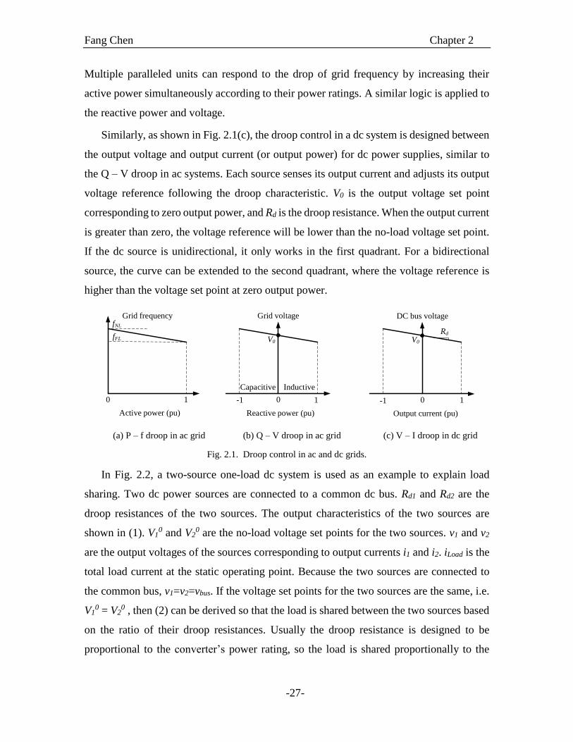
Fang Chen Chapter 2
-27-
Multiple paralleled units can respond to the drop of grid frequency by increasing their
active power simultaneously according to their power ratings. A similar logic is applied to
the reactive power and voltage.
Similarly, as shown in Fig. 2.1(c), the droop control in a dc system is designed between
the output voltage and output current (or output power) for dc power supplies, similar to
the Q – V droop in ac systems. Each source senses its output current and adjusts its output
voltage reference following the droop characteristic. V0 is the output voltage set point
corresponding to zero output power, and Rd is the droop resistance. When the output current
is greater than zero, the voltage reference will be lower than the no-load voltage set point.
If the dc source is unidirectional, it only works in the first quadrant. For a bidirectional
source, the curve can be extended to the second quadrant, where the voltage reference is
higher than the voltage set point at zero output power.
Grid frequency
Active power (pu)
0 1
fNL
fFL
Grid voltage
Reactive power (pu)
0
InductiveCapacitive
V0
DC bus voltage
Output current (pu)
0
V0
1-1
Rd
1-1
(a) P – f droop in ac grid (b) Q – V droop in ac grid (c) V – I droop in dc grid
Fig. 2.1. Droop control in ac and dc grids.
In Fig. 2.2, a two-source one-load dc system is used as an example to explain load
sharing. Two dc power sources are connected to a common dc bus. Rd1 and Rd2 are the
droop resistances of the two sources. The output characteristics of the two sources are
shown in (1). V10 and V2
0 are the no-load voltage set points for the two sources. v1 and v2
are the output voltages of the sources corresponding to output currents i1 and i2. iLoad is the
total load current at the static operating point. Because the two sources are connected to
the common bus, v1=v2=vbus. If the voltage set points for the two sources are the same, i.e.
V10 = V2
0 , then (2) can be derived so that the load is shared between the two sources based
on the ratio of their droop resistances. Usually the droop resistance is designed to be
proportional to the converter’s power rating, so the load is shared proportionally to the
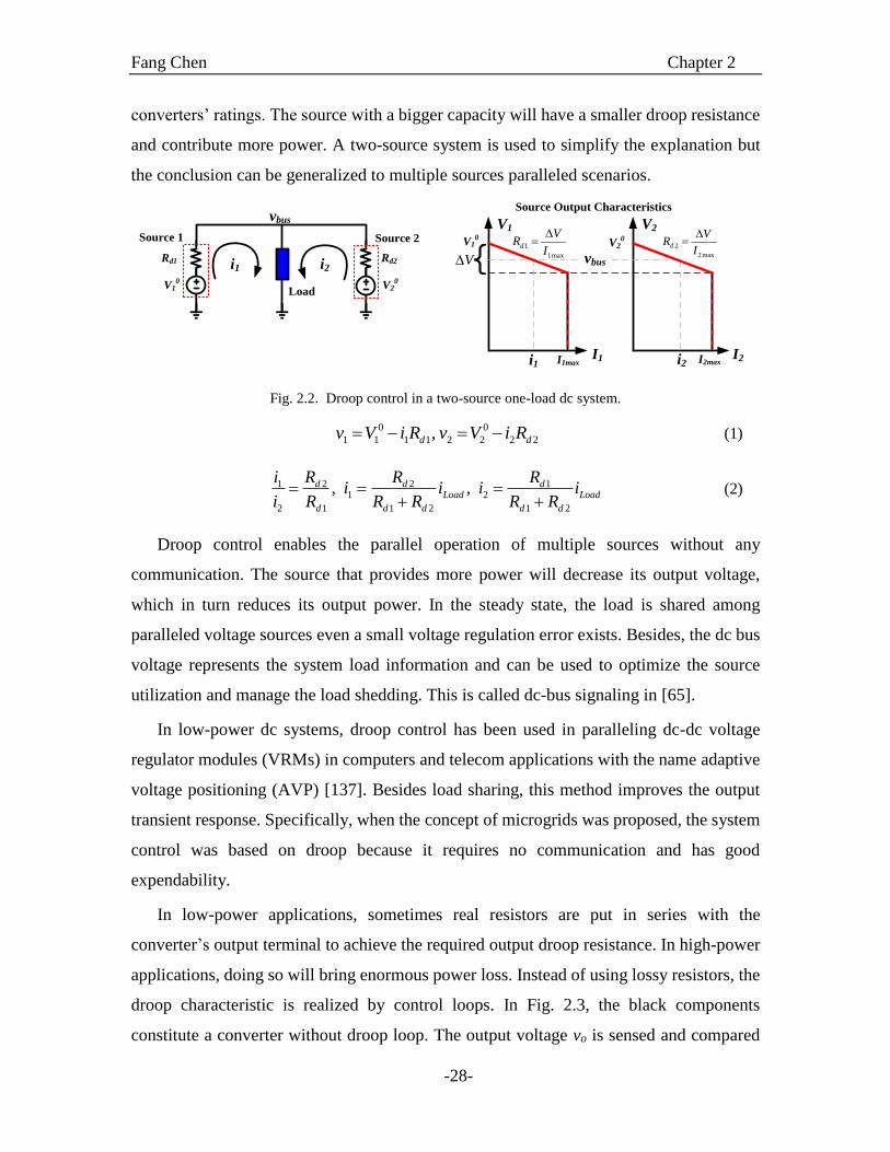
Fang Chen Chapter 2
-28-
converters’ ratings. The source with a bigger capacity will have a smaller droop resistance
and contribute more power. A two-source system is used to simplify the explanation but
the conclusion can be generalized to multiple sources paralleled scenarios.
LoadV1
0
i1 i2Rd1 Rd2
vbus
Source 1 Source 2
V20
Source Output Characteristics
V1
I1I1max
V10
V2
I2max
V20
I2
vbus
i1 i2
V1
1max
d
VR
I
2
2 max
d
VR
I
Fig. 2.2. Droop control in a two-source one-load dc system.
0 0
1 1 1 1 2 2 2 2,d dv V i R v V i R (1)
1 2 2 11 2
2 1 1 2 1 2
, ,d d dLoad Load
d d d d d
i R R Ri i i i
i R R R R R
(2)
Droop control enables the parallel operation of multiple sources without any
communication. The source that provides more power will decrease its output voltage,
which in turn reduces its output power. In the steady state, the load is shared among
paralleled voltage sources even a small voltage regulation error exists. Besides, the dc bus
voltage represents the system load information and can be used to optimize the source
utilization and manage the load shedding. This is called dc-bus signaling in [65].
In low-power dc systems, droop control has been used in paralleling dc-dc voltage
regulator modules (VRMs) in computers and telecom applications with the name adaptive
voltage positioning (AVP) [137]. Besides load sharing, this method improves the output
transient response. Specifically, when the concept of microgrids was proposed, the system
control was based on droop because it requires no communication and has good
expendability.
In low-power applications, sometimes real resistors are put in series with the
converter’s output terminal to achieve the required output droop resistance. In high-power
applications, doing so will bring enormous power loss. Instead of using lossy resistors, the
droop characteristic is realized by control loops. In Fig. 2.3, the black components
constitute a converter without droop loop. The output voltage vo is sensed and compared
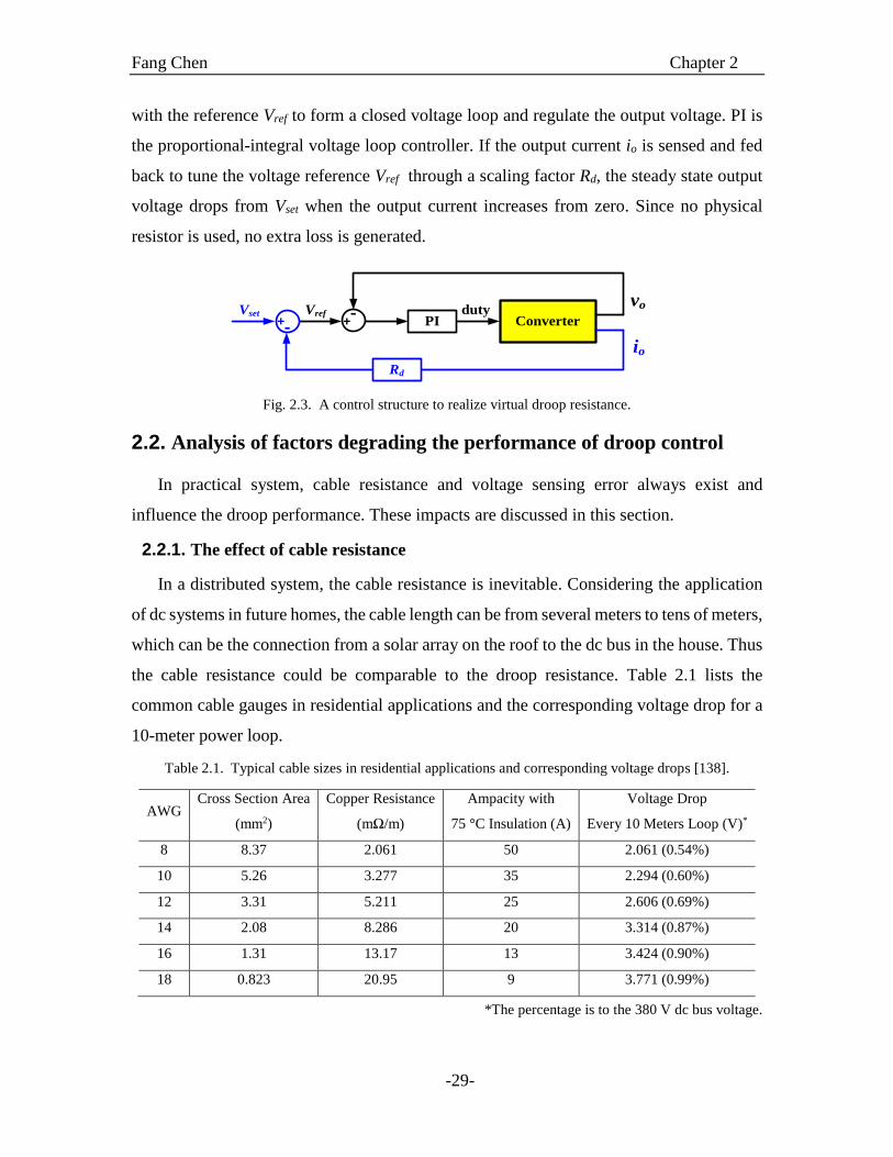
Fang Chen Chapter 2
-29-
with the reference Vref to form a closed voltage loop and regulate the output voltage. PI is
the proportional-integral voltage loop controller. If the output current io is sensed and fed
back to tune the voltage reference Vref through a scaling factor Rd, the steady state output
voltage drops from Vset when the output current increases from zero. Since no physical
resistor is used, no extra loss is generated.
dutyConverterPI
voVref+- +-Vset
io
Rd
Fig. 2.3. A control structure to realize virtual droop resistance.
2.2. Analysis of factors degrading the performance of droop control
In practical system, cable resistance and voltage sensing error always exist and
influence the droop performance. These impacts are discussed in this section.
2.2.1. The effect of cable resistance
In a distributed system, the cable resistance is inevitable. Considering the application
of dc systems in future homes, the cable length can be from several meters to tens of meters,
which can be the connection from a solar array on the roof to the dc bus in the house. Thus
the cable resistance could be comparable to the droop resistance. Table 2.1 lists the
common cable gauges in residential applications and the corresponding voltage drop for a
10-meter power loop.
Table 2.1. Typical cable sizes in residential applications and corresponding voltage drops [138].
AWG Cross Section Area
(mm2)
Copper Resistance
(mΩ/m)
Ampacity with
75 °C Insulation (A)
Voltage Drop
Every 10 Meters Loop (V)*
8 8.37 2.061 50 2.061 (0.54%)
10 5.26 3.277 35 2.294 (0.60%)
12 3.31 5.211 25 2.606 (0.69%)
14 2.08 8.286 20 3.314 (0.87%)
16 1.31 13.17 13 3.424 (0.90%)
18 0.823 20.95 9 3.771 (0.99%)
*The percentage is to the 380 V dc bus voltage.
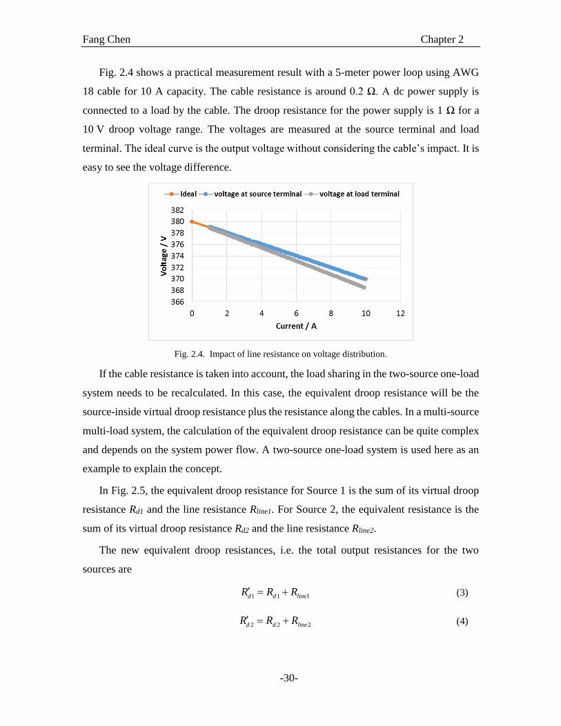
Fang Chen Chapter 2
-30-
Fig. 2.4 shows a practical measurement result with a 5-meter power loop using AWG
18 cable for 10 A capacity. The cable resistance is around 0.2 Ω. A dc power supply is
connected to a load by the cable. The droop resistance for the power supply is 1 Ω for a
10 V droop voltage range. The voltages are measured at the source terminal and load
terminal. The ideal curve is the output voltage without considering the cable’s impact. It is
easy to see the voltage difference.
Fig. 2.4. Impact of line resistance on voltage distribution.
If the cable resistance is taken into account, the load sharing in the two-source one-load
system needs to be recalculated. In this case, the equivalent droop resistance will be the
source-inside virtual droop resistance plus the resistance along the cables. In a multi-source
multi-load system, the calculation of the equivalent droop resistance can be quite complex
and depends on the system power flow. A two-source one-load system is used here as an
example to explain the concept.
In Fig. 2.5, the equivalent droop resistance for Source 1 is the sum of its virtual droop
resistance Rd1 and the line resistance Rline1. For Source 2, the equivalent resistance is the
sum of its virtual droop resistance Rd2 and the line resistance Rline2.
The new equivalent droop resistances, i.e. the total output resistances for the two
sources are
1 1 1d d lineR R R (3)
2 2 2d d lineR R R (4)
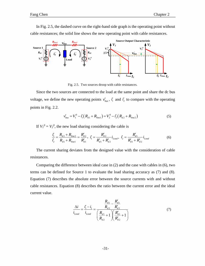
Fang Chen Chapter 2
-31-
In Fig. 2.5, the dashed curve on the right-hand side graph is the operating point without
cable resistances; the solid line shows the new operating point with cable resistances.
Load
Source Output Characteristic
V1
I1I1max
V10
V2
I2max
V20
I2
vbus
i1 i2
V
V10
i1 i2Rd1 Rd2
vbus
Source 1 Source 2
V20
Rline1 Rline2
' '
'
' '
'
Fig. 2.5. Two sources droop with cable resistances.
Since the two sources are connected to the load at the same point and share the dc bus
voltage, we define the new operating points busv , 1i and 2i to compare with the operating
points in Fig. 2.2.
0 0
1 1 1 1 2 2 2 2bus d line d linev V i R R V i R R (5)
If V10 = V2
0, the new load sharing considering the cable is
1 2 2 2 2 11 2
2 1 1 1 1 2 1 2
,d line d d dLoad Load
d line d d d d d
i R R R R Ri i i i
i R R R R R R R
, (6)
The current sharing deviates from the designed value with the consideration of cable
resistances.
Comparing the difference between ideal case in (2) and the case with cables in (6), two
terms can be defined for Source 1 to evaluate the load sharing accuracy as (7) and (8).
Equation (7) describes the absolute error between the source currents with and without
cable resistances. Equation (8) describes the ratio between the current error and the ideal
current value.
1 1
1 1 2 2
1 1
2 2
1 1
d d
d d
Load Load d d
d d
R R
i i i R R
i i R R
R R
(7)
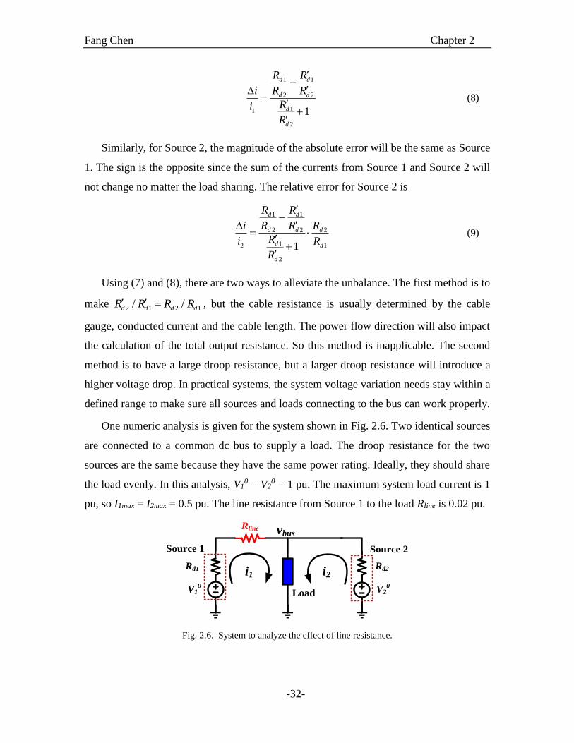
Fang Chen Chapter 2
-32-
1 1
2 2
11
2
1
d d
d d
d
d
R R
i R R
Ri
R
(8)
Similarly, for Source 2, the magnitude of the absolute error will be the same as Source
1. The sign is the opposite since the sum of the currents from Source 1 and Source 2 will
not change no matter the load sharing. The relative error for Source 2 is
1 1
22 2
12 1
2
1
d d
dd d
d d
d
R R
i RR R
Ri R
R
(9)
Using (7) and (8), there are two ways to alleviate the unbalance. The first method is to
make 2 1 2 1/ /d d d dR R R R , but the cable resistance is usually determined by the cable
gauge, conducted current and the cable length. The power flow direction will also impact
the calculation of the total output resistance. So this method is inapplicable. The second
method is to have a large droop resistance, but a larger droop resistance will introduce a
higher voltage drop. In practical systems, the system voltage variation needs stay within a
defined range to make sure all sources and loads connecting to the bus can work properly.
One numeric analysis is given for the system shown in Fig. 2.6. Two identical sources
are connected to a common dc bus to supply a load. The droop resistance for the two
sources are the same because they have the same power rating. Ideally, they should share
the load evenly. In this analysis, V10 = V2
0 = 1 pu. The maximum system load current is 1
pu, so I1max = I2max = 0.5 pu. The line resistance from Source 1 to the load Rline is 0.02 pu.
LoadV10
i1 i2Rd1 Rd2
vbus
Source 1 Source 2
V20
Rline
Fig. 2.6. System to analyze the effect of line resistance.
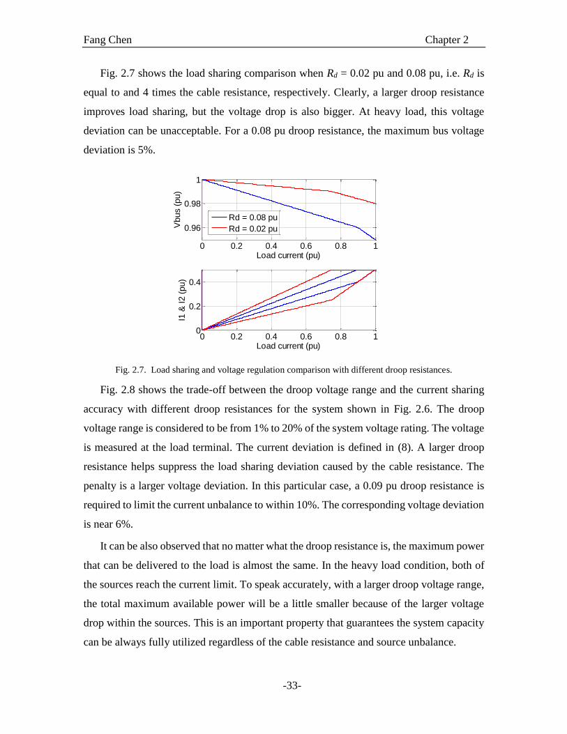
Fang Chen Chapter 2
-33-
Fig. 2.7 shows the load sharing comparison when Rd = 0.02 pu and 0.08 pu, i.e. Rd is
equal to and 4 times the cable resistance, respectively. Clearly, a larger droop resistance
improves load sharing, but the voltage drop is also bigger. At heavy load, this voltage
deviation can be unacceptable. For a 0.08 pu droop resistance, the maximum bus voltage
deviation is 5%.
Fig. 2.7. Load sharing and voltage regulation comparison with different droop resistances.
Fig. 2.8 shows the trade-off between the droop voltage range and the current sharing
accuracy with different droop resistances for the system shown in Fig. 2.6. The droop
voltage range is considered to be from 1% to 20% of the system voltage rating. The voltage
is measured at the load terminal. The current deviation is defined in (8). A larger droop
resistance helps suppress the load sharing deviation caused by the cable resistance. The
penalty is a larger voltage deviation. In this particular case, a 0.09 pu droop resistance is
required to limit the current unbalance to within 10%. The corresponding voltage deviation
is near 6%.
It can be also observed that no matter what the droop resistance is, the maximum power
that can be delivered to the load is almost the same. In the heavy load condition, both of
the sources reach the current limit. To speak accurately, with a larger droop voltage range,
the total maximum available power will be a little smaller because of the larger voltage
drop within the sources. This is an important property that guarantees the system capacity
can be always fully utilized regardless of the cable resistance and source unbalance.
0 0.2 0.4 0.6 0.8 1
0.96
0.98
1
Load current (pu)
Vbus (
pu)
Rd = 0.08 pu
Rd = 0.02 pu
0 0.2 0.4 0.6 0.8 10
0.2
0.4
Load current (pu)
I1 &
I2 (
pu)
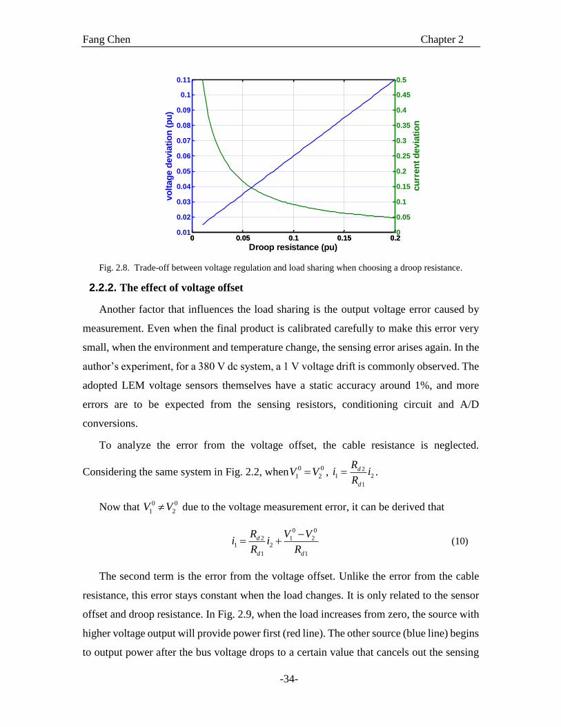
Fang Chen Chapter 2
-34-
Fig. 2.8. Trade-off between voltage regulation and load sharing when choosing a droop resistance.
2.2.2. The effect of voltage offset
Another factor that influences the load sharing is the output voltage error caused by
measurement. Even when the final product is calibrated carefully to make this error very
small, when the environment and temperature change, the sensing error arises again. In the
author’s experiment, for a 380 V dc system, a 1 V voltage drift is commonly observed. The
adopted LEM voltage sensors themselves have a static accuracy around 1%, and more
errors are to be expected from the sensing resistors, conditioning circuit and A/D
conversions.
To analyze the error from the voltage offset, the cable resistance is neglected.
Considering the same system in Fig. 2.2, when0 0
1 2V V , 21 2
1
d
d
Ri i
R .
Now that 0 0
1 2V V due to the voltage measurement error, it can be derived that
0 0
2 1 21 2
1 1
d
d d
R V Vi i
R R
(10)
The second term is the error from the voltage offset. Unlike the error from the cable
resistance, this error stays constant when the load changes. It is only related to the sensor
offset and droop resistance. In Fig. 2.9, when the load increases from zero, the source with
higher voltage output will provide power first (red line). The other source (blue line) begins
to output power after the bus voltage drops to a certain value that cancels out the sensing
0 0.05 0.1 0.15 0.20.01
0.02
0.03
0.04
0.05
0.06
0.07
0.08
0.09
0.1
0.11
Droop resistance (pu)
vo
ltag
e d
evia
tio
n (
pu
)
0 0.05 0.1 0.15 0.20
0.05
0.1
0.15
0.2
0.25
0.3
0.35
0.4
0.45
0.5
cu
rren
t d
evia
tio
n
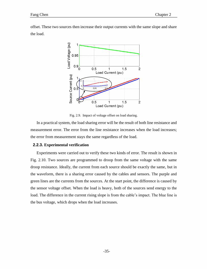
Fang Chen Chapter 2
-35-
offset. These two sources then increase their output currents with the same slope and share
the load.
Fig. 2.9. Impact of voltage offset on load sharing.
In a practical system, the load sharing error will be the result of both line resistance and
measurement error. The error from the line resistance increases when the load increases;
the error from measurement stays the same regardless of the load.
2.2.3. Experimental verification
Experiments were carried out to verify these two kinds of error. The result is shown in
Fig. 2.10. Two sources are programmed to droop from the same voltage with the same
droop resistance. Ideally, the current from each source should be exactly the same, but in
the waveform, there is a sharing error caused by the cables and sensors. The purple and
green lines are the currents from the sources. At the start point, the difference is caused by
the sensor voltage offset. When the load is heavy, both of the sources send energy to the
load. The difference in the current rising slope is from the cable’s impact. The blue line is
the bus voltage, which drops when the load increases.

Fang Chen Chapter 2
-36-
DC bus voltage (5V/div)
5V
Start point difference
Source 1&2 current (5A/div)
Slope difference
Fig. 2.10. Load sharing experiment with line resistance and measurement error.
2.3. Quantitative analysis for two-source systems
As discussed above, the droop voltage range and cable resistance impact the steady-
state load sharing among sources. It is important for a system designer to choose proper
cables and design a corresponding droop voltage range. In practice, the cable size is usually
chosen based on the maximum current, so the main task for the designer is to choose a
proper droop voltage range. It has been shown that a larger droop range helps reduce the
load sharing unbalance, but the trade-off is a bigger voltage deviation on the dc bus. There
exists a compromise between the two targets. It is thus useful to have the worst case
analyzed so that the designer can then use the result to choose a droop voltage range and
guarantee the required sharing accuracy, even under the worst conditions.
2.3.1. Identification of the worst source and load locations
To analyze the worst-case scenario for a two-source system, the worst load and source
placement need to be identified first. Looking at (7) and (8), in a practical system, the droop
resistance ratio 1 2/d dR R is designed by the power ratings of sources to ensure the load is
shared between sources according to their power ratings. Thus the only variable is the ratio
1 2/d dR R . If we calculate the derivative of (7) and (8) with respect to 1 2/d dR R , we find both
of them are smaller than zero, which means they are decreasing functions. Thus the worst
case can be identified as shown in Fig. 2.11. In the graph, Rs1-b and Rs2-b are the cable
resistances from the two sources to the points where they connect the bus, Rbus is the total
bus resistance from one terminal to the other, and Rb-l is the resistance from the bus to the
load. This result is reasonable and easy to understand. The worst case occurs when the two
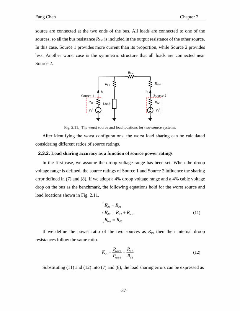
Fang Chen Chapter 2
-37-
source are connected at the two ends of the bus. All loads are connected to one of the
sources, so all the bus resistance Rbus is included in the output resistance of the other source.
In this case, Source 1 provides more current than its proportion, while Source 2 provides
less. Another worst case is the symmetric structure that all loads are connected near
Source 2.
V10
Load
i1 i2
Rd1 Rd2
Source 1 Source 2
V20
Rs2-b
Rbus
Rb-l
Fig. 2.11. The worst source and load locations for two-source systems.
After identifying the worst configurations, the worst load sharing can be calculated
considering different ratios of source ratings.
2.3.2. Load sharing accuracy as a function of source power ratings
In the first case, we assume the droop voltage range has been set. When the droop
voltage range is defined, the source ratings of Source 1 and Source 2 influence the sharing
error defined in (7) and (8). If we adopt a 4% droop voltage range and a 4% cable voltage
drop on the bus as the benchmark, the following equations hold for the worst source and
load locations shown in Fig. 2.11.
1 1
2 2
2
d d
d d bus
bus d
R R
R R R
R R
(11)
If we define the power ratio of the two sources as Kp, then their internal droop
resistances follow the same ratio.
1 2
2 1
rate dP
rate d
P RK
P R (12)
Substituting (11) and (12) into (7) and (8), the load sharing errors can be expressed as
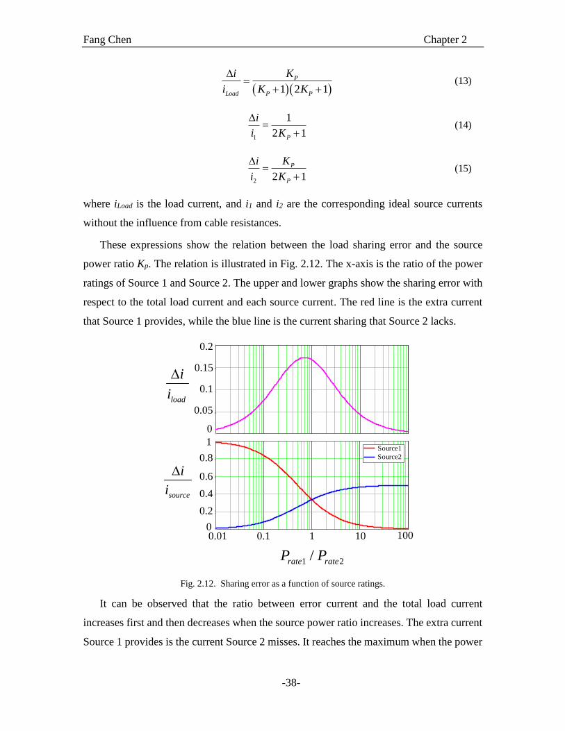
Fang Chen Chapter 2
-38-
1 2 1
P
Load P P
i K
i K K
(13)
1
1
2 1P
i
i K
(14)
2 2 1
P
P
i K
i K
(15)
where iLoad is the load current, and i1 and i2 are the corresponding ideal source currents
without the influence from cable resistances.
These expressions show the relation between the load sharing error and the source
power ratio Kp. The relation is illustrated in Fig. 2.12. The x-axis is the ratio of the power
ratings of Source 1 and Source 2. The upper and lower graphs show the sharing error with
respect to the total load current and each source current. The red line is the extra current
that Source 1 provides, while the blue line is the current sharing that Source 2 lacks.
0
0.05
0.1
0.15
0.2
dI/
Ilo
ad
0.01 0.1 1 10 1000
0.2
0.4
0.6
0.8
Source1
Source2
P1max/P2max
dI/
Is
0
0.05
0.1
0.15
0.2
dI/
Ilo
ad
0.01 0.1 1 10 1000
0.2
0.4
0.6
0.8
Source1
Source2
P1max/P2max
dI/
Is
1 2/rate rateP P
0.01 0.1 1 10 1000
0.2
0.4
0.6
0.8
1
0
0.05
0.1
0.15
0.2
source
i
i
load
i
i
Fig. 2.12. Sharing error as a function of source ratings.
It can be observed that the ratio between error current and the total load current
increases first and then decreases when the source power ratio increases. The extra current
Source 1 provides is the current Source 2 misses. It reaches the maximum when the power

Fang Chen Chapter 2
-39-
ratio is a certain value between negative infinity and positive infinity. In this case, the error
reaches the maximum when P1/P2 equals to 0.707, and the error is 0.172, i.e. 17.2%.
On the other hand, the relative error for Source 1 reduces from 100% to 0% when the
power ratio between Sources 1 and 2 increases. This makes sense, since the base value i1
increases when the Source 1 rating increases. In the worst case, when Source 1 is very
small, it can take almost 100% more current than the value it should take. Source 2 loses
50% of its current sharing in the worst case.
In conclusion, to evaluate the load sharing of a multiple source system, the error current
as a percent of the total current, i.e. Δi/iLoad, is a good indicator.
2.3.3. Load sharing accuracy as a function of droop voltage range
Now we can look at the original problem of how to choose a proper droop voltage range
so the unbalance is within a designed range. Assume the droop voltage range Vdroop is KV
times higher than the maximum possible line voltage drop Vline such that
droop V lineV K V (16)
Then the following resistance relation exists for the worst case shown in Fig. 2.11.
2d V lineR K R (17)
Following the same procedure, we can derive the function about the sharing error. The
ratio between the current error and the total load current is
,
1 1
P V P
Load P V P V
i K K K
i K K K K
(18)
Making ,
0P V
P
i K K
K
, the maximum of Δi/iLoad occurs when
1
VP
V
KK
K
. The
maximum value is
2
1
1
V
LoadV V
i K
i K K
(19)
Then we can draw the current error as a function of droop voltage range and
corresponding source power in Fig. 2.13. In the top graph, the picture shows the error
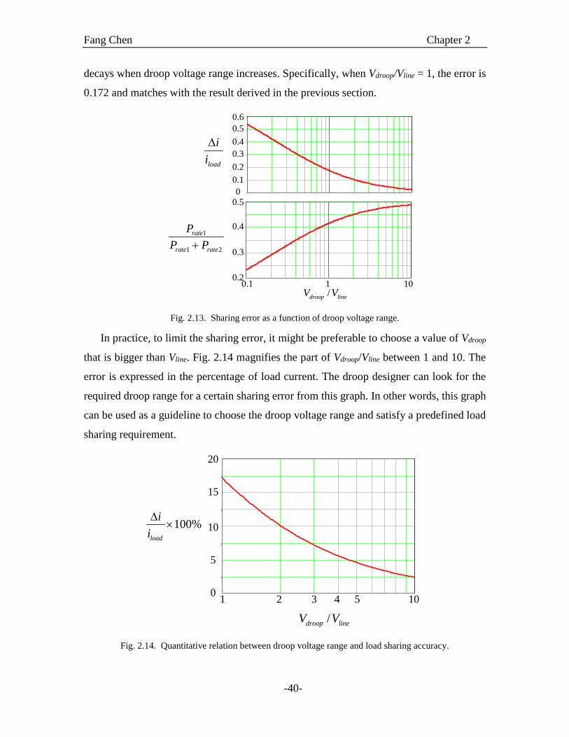
Fang Chen Chapter 2
-40-
decays when droop voltage range increases. Specifically, when Vdroop/Vline = 1, the error is
0.172 and matches with the result derived in the previous section.
0
0.1
0.2
0.3
0.4
0.5
0.6
dI_
max
(p
.u.)
0.1 1 100.2
0.25
0.3
0.35
0.4
0.45
0.5
V_droop/V_line
P_s
ou
rce
(p.u
.)
0.1 1 10/droop lineV V
0
0.1
0.2
0.3
0.4
0.5
0.6
0.2
0.3
0.4
0.5
load
i
i
1
1 2
rate
rate rate
P
P P
Fig. 2.13. Sharing error as a function of droop voltage range.
In practice, to limit the sharing error, it might be preferable to choose a value of Vdroop
that is bigger than Vline. Fig. 2.14 magnifies the part of Vdroop/Vline between 1 and 10. The
error is expressed in the percentage of load current. The droop designer can look for the
required droop range for a certain sharing error from this graph. In other words, this graph
can be used as a guideline to choose the droop voltage range and satisfy a predefined load
sharing requirement.
1 100
2.5
5
7.5
10
12.5
15
17.5
20
dI_
max
(p.
u.)
/droop lineV V
1 102 3 4 50
5
10
15
20
100%load
i
i
Fig. 2.14. Quantitative relation between droop voltage range and load sharing accuracy.
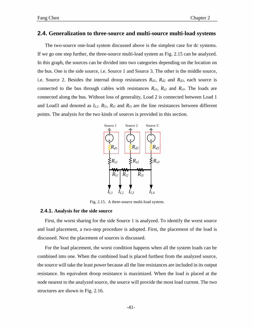
Fang Chen Chapter 2
-41-
2.4. Generalization to three-source and multi-source multi-load systems
The two-source one-load system discussed above is the simplest case for dc systems.
If we go one step further, the three-source multi-load system as Fig. 2.15 can be analyzed.
In this graph, the sources can be divided into two categories depending on the location on
the bus. One is the side source, i.e. Source 1 and Source 3. The other is the middle source,
i.e. Source 2. Besides the internal droop resistances Rd1, Rd2 and Rd3, each source is
connected to the bus through cables with resistances Rs1, Rs2 and Rs3. The loads are
connected along the bus. Without loss of generality, Load 2 is connected between Load 1
and Load3 and denoted as IL2. Rl1, Rl2 and Rl3 are the line resistances between different
points. The analysis for the two kinds of sources is provided in this section.
Rd1
Rs1
IL1
Source 1
Rd2
Rs2
Source 2
Rd3
Rs3
Source 3
IL2 IL3 IL4
Rl1 Rl2 Rl3
Fig. 2.15. A three-source multi-load system.
2.4.1. Analysis for the side source
First, the worst sharing for the side Source 1 is analyzed. To identify the worst source
and load placement, a two-step procedure is adopted. First, the placement of the load is
discussed. Next the placement of sources is discussed.
For the load placement, the worst condition happens when all the system loads can be
combined into one. When the combined load is placed furthest from the analyzed source,
the source will take the least power because all the line resistances are included in its output
resistance. Its equivalent droop resistance is maximized. When the load is placed at the
node nearest to the analyzed source, the source will provide the most load current. The two
structures are shown in Fig. 2.16.

Fang Chen Chapter 2
-42-
Rd1
Rs1
IL1
Source 1
Rd2
Rs2
Source 2
Rd3
Rs3
Source 3
Rl1 Rl2 Rl3
Rd1
Rs1
Source 1
Rd2
Rs2
Source 2
Rd3
Rs3
Source 3
IL4
Rl1 Rl2 Rl3
(a) More current sharing (b) Less current sharing
Fig. 2.16. Two extreme cases for side Source 1.
In the case of Fig. 2.16(a), Source 1 takes more current than its power proportion. The
graph can be further simplified by analyzing the source and cable placement. First, to
maximize the current for Source 1, its output resistance should be minimized, which means
Rs1 equals zero. On the other hand, the total output resistance for Source 2 and Source 3
should be maximized, so Rs2 and Rs3 should be maximized. To maximize the total output
resistance of Source 2 paralleled with Source 3, it can be proved that both the sources
should be connected to the furthest end of the bus as Fig. 2.17(a). Using Thevenin’s
theorem, the circuit can be simplified as Fig. 2.17(b). After combining the two sources, the
new droop resistance of the combined source is Rd2 paralleled with Rd3. The new source
branch resistance is Rs2 paralleled with Rs3. Moreover, the simplified circuit still complies
with the load sharing property, so that
2 3 2 3
2 3 2 31/ 1/ 1/ ||
s s s s
d d d d
I I I I
R R R R
(20)
where Is2 and Is3 are the steady-state load sharing of the two sources.
This means that in the worst case, the three-source system can actually be simplified as
the two-source system that has been discussed above. Thus the worst-case analysis results
and design guidelines for the two-source system can be used for this three-source system.

Fang Chen Chapter 2
-43-
Rd1
IL1
Source 1
Rd2
Rs2
Source 2
Rd3
Rs3
Source 3
Rl1 Rl2 Rl3
Rd1
IL1
Source 1
Rd2||Rd3
Rs2||Rs3
Source 2+3
Rl1 Rl2 Rl3
Is2+Is3
(a) The worst source placement (b) Thevenin’s equivalent circuit
Fig. 2.17. Source placement and combination for the most current sharing from Source 1.
In the case of Fig. 2.16(b), Source 1 takes less current. This scenario can be analyzed
in a similar way and has the same worst-case result.
2.4.2. Analysis for the middle source
For analysis of the middle source, the result is a little different. The two extreme cases
for the middle source are shown in Fig. 2.18. For the case in Fig. 2.18(a), where the load
is connected close to Source 2, Source 2 will take more load current. The analysis is
identical as the side source. For the case in Fig. 2.18(b), Source 2 will take less load current.
The worst-case analysis is shown below.
Rd1
Rs1
Source 1
Rd2
Rs2
Source 2
Rd3
Rs3
Source 3
IL3
Rl1 Rl2 Rl3
Rd1
Rs1
IL1
Source 1
Rd2
Rs2
Source 2
Rd3
Rs3
Source 3
Rl1 Rl2 Rl3
(a) More current sharing (b) Less current sharing
Fig. 2.18. Two worst cases for the middle source.
In Fig. 2.18(b), in order to let Source 2 take the least current, it can be seen that Rs1
needs to be eliminated and Rs2 needs to be maximized, but the evaluation of Rs3 is not
obvious. Having the largest Rs3 means the total current from Source 2 and Source 3 is
minimized. However, comparing Sources 2 and 3, Source 2 takes the most current. Thus

Fang Chen Chapter 2
-44-
in this case, using the largest Rs3 does not guarantee that Source 2 takes the least current.
In fact, the current from Source 2 can be expressed as
1 3 12
1 2 3 2 3 21 2
3
||1
sd sd sds
sd l sd sd sd sd sdsd l sd
sd
R R RI
R R R R R R RR R R
R
(21)
where
1 2 3
, 1, 2, 3sdi di si
l l l l
R R R i
R R R R
Is2 is minimized when Rsd3 is minimized. In other words, Rs3 is zero. Hence the worst
scenario is identified in Fig. 2.19. In this case, the error current will not be as large as the
worst case for side sources because the total output resistance for Source 1 and Source 3 is
not minimized.
Rd1
IL1
Source 1
Rd2
Rs2
Source 2
Rd3
Rs3
Source 3
Rl1 Rl2 Rl3
Rd1
IL1
Source 1
Rd2
Rs2
Source 2
Rd3
Source 3
Rl1 Rl2 Rl3
(a) Worst-case source placement (b) Worst-case cable arrangement
Fig. 2.19. The worst source and cable placement for the middle source to take the least load.
In all, the most severe unbalance in a three-source system occurs for the side source
and the result is the same as the two-source analysis.
2.4.3. Generalization to multi-source system
For a general multi-source multi-load system, the methodology is the same. The worst
load distribution occurs when all loads are connected to the same point and the connection
point should be either nearest or furthest to the analyzed source. For the source distribution,
the worst case occurs for the side source when all the other sources are connected to the

Fang Chen Chapter 2
-45-
other end of the bus. Under this condition, the worst case occurs, and the result is the same
as the two-source one-load system shown in Fig. 2.20.
Source 1 Source 2 Source m
Load 1 Load 2 Load n
Source 1 Source 2
Load
(a) General structure of a multi-source multi-load system (b) Worst scenario
Fig. 2.20. A multi-source multi-load system and its worst case.
2.5. Proposed droop design guidelines for dc systems
As discussed in the previous sections, the worst-case scenario of two-source systems
can be used to typify the worst case of multi-source, multi-load systems. The quantitative
relation between the droop voltage range and load sharing accuracy in Fig. 2.13 and Fig.
2.14 can thus be used for a general dc system droop design.
In a dc system, the voltage drop from source to load terminals consists of two parts:
Total voltage drop = cable voltage drop + droop voltage drop
Based on the National Electric Code (NEC) recommendation, “the maximum
combined voltage drop for both the feeder and branch circuit shouldn't exceed 5%” [139].
Considering the normal length for cabling, it is reasonable to assign this 5% voltage drop
to different cable segments like the following ratio so the total bus voltage drop is limited.
Total 5% cable voltage drop = 2% (source to bus) + 2% (along bus) + 1% (bus to
load)
The choice of the size for each segment of cable can follow a two-step procedure. The
bottom line is to satisfy the current capability, i.e. the thermal requirement. The cable needs
to be able to carry the designed maximum current. Then the voltage drop during the
heaviest load condition needs to be checked. If the voltage drop requirement is not satisfied,
then a thicker wire needs to be chosen. In practice, unless the transmission distance is very
long, the voltage drop requirement is usually weaker than the size decided by thermal
constraints.
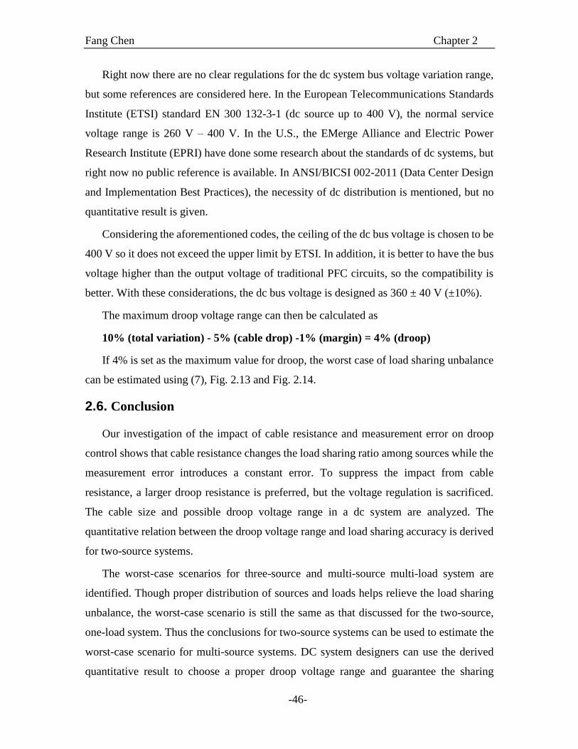
Fang Chen Chapter 2
-46-
Right now there are no clear regulations for the dc system bus voltage variation range,
but some references are considered here. In the European Telecommunications Standards
Institute (ETSI) standard EN 300 132-3-1 (dc source up to 400 V), the normal service
voltage range is 260 V – 400 V. In the U.S., the EMerge Alliance and Electric Power
Research Institute (EPRI) have done some research about the standards of dc systems, but
right now no public reference is available. In ANSI/BICSI 002-2011 (Data Center Design
and Implementation Best Practices), the necessity of dc distribution is mentioned, but no
quantitative result is given.
Considering the aforementioned codes, the ceiling of the dc bus voltage is chosen to be
400 V so it does not exceed the upper limit by ETSI. In addition, it is better to have the bus
voltage higher than the output voltage of traditional PFC circuits, so the compatibility is
better. With these considerations, the dc bus voltage is designed as 360 ± 40 V (±10%).
The maximum droop voltage range can then be calculated as
10% (total variation) - 5% (cable drop) -1% (margin) = 4% (droop)
If 4% is set as the maximum value for droop, the worst case of load sharing unbalance
can be estimated using (7), Fig. 2.13 and Fig. 2.14.
2.6. Conclusion
Our investigation of the impact of cable resistance and measurement error on droop
control shows that cable resistance changes the load sharing ratio among sources while the
measurement error introduces a constant error. To suppress the impact from cable
resistance, a larger droop resistance is preferred, but the voltage regulation is sacrificed.
The cable size and possible droop voltage range in a dc system are analyzed. The
quantitative relation between the droop voltage range and load sharing accuracy is derived
for two-source systems.
The worst-case scenarios for three-source and multi-source multi-load system are
identified. Though proper distribution of sources and loads helps relieve the load sharing
unbalance, the worst-case scenario is still the same as that discussed for the two-source,
one-load system. Thus the conclusions for two-source systems can be used to estimate the
worst-case scenario for multi-source systems. DC system designers can use the derived
quantitative result to choose a proper droop voltage range and guarantee the sharing

Fang Chen Chapter 2
-47-
accuracy within a required range. If necessary, the detailed load sharing result and voltage
distribution for a particular configuration can be calculated using numerical methods.
Fang Chen Chapter 3
-48-
Chapter 3. A NONLINEAR DROOP CONTROL TO IMPROVE
LOAD SHARING AND VOLTAGE REGULATION
The traditional droop design requires the trade-off between voltage regulation and load
sharing. Using a larger droop resistance improves the load sharing but requires a larger dc
bus voltage range. Reducing the droop resistance improves the bus regulation but sacrifices
the accuracy of load sharing. In a practical design, the designer needs to evaluate the
requirements and make a compromise. To solve this issue, instead of using constant droop
resistance, this chapter proposes using a nonlinear droop method.
In the proposed nonlinear droop, the value of the droop resistance is a function of the
output current, which increases automatically when the converter’s output current increases.
By doing so, the impacts from the sensor and cable are greatly reduced and the load sharing
is better under heavy load. Furthermore, the dc bus voltage regulation is improved and has
smaller deviation. As a result, the voltage variation on the dc bus is reduced, while load
sharing is still guaranteed. The proposed method needs only the local output current
information, so the advantage of traditional droop control is preserved.
In this chapter, different second-order droop functions are evaluated and compared.
The effectiveness of the proposed droop methods is verified by simulation and experiment.
The experimental results prove the nonlinear droop method has better load sharing under
heavy load and tighter bus voltage regulation under light load.
To evaluate the impact of nonlinear droop control on system dynamic and stability, a
detailed output impedance model is derived for dc-dc converters. Using a buck converter
as an example, the output impedances with different droop profiles are modeled and
measured by experiment. The measurement results match with the model very well.
3.1. Review of techniques to improve the load sharing and voltage
regulation of droop control
To improve the load sharing and voltage regulation of droop control, a lot of research
has been done. Generally speaking, these improvements can be classified into
communication-less and communication-based methods.
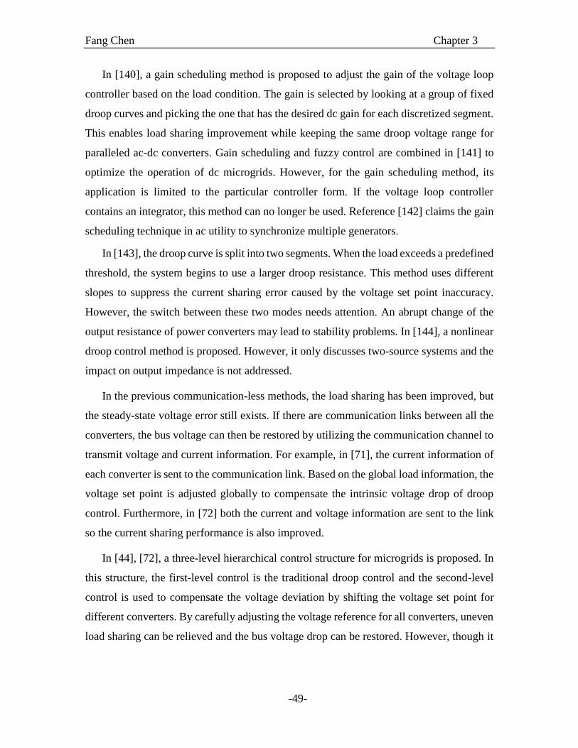
Fang Chen Chapter 3
-49-
In [140], a gain scheduling method is proposed to adjust the gain of the voltage loop
controller based on the load condition. The gain is selected by looking at a group of fixed
droop curves and picking the one that has the desired dc gain for each discretized segment.
This enables load sharing improvement while keeping the same droop voltage range for
paralleled ac-dc converters. Gain scheduling and fuzzy control are combined in [141] to
optimize the operation of dc microgrids. However, for the gain scheduling method, its
application is limited to the particular controller form. If the voltage loop controller
contains an integrator, this method can no longer be used. Reference [142] claims the gain
scheduling technique in ac utility to synchronize multiple generators.
In [143], the droop curve is split into two segments. When the load exceeds a predefined
threshold, the system begins to use a larger droop resistance. This method uses different
slopes to suppress the current sharing error caused by the voltage set point inaccuracy.
However, the switch between these two modes needs attention. An abrupt change of the
output resistance of power converters may lead to stability problems. In [144], a nonlinear
droop control method is proposed. However, it only discusses two-source systems and the
impact on output impedance is not addressed.
In the previous communication-less methods, the load sharing has been improved, but
the steady-state voltage error still exists. If there are communication links between all the
converters, the bus voltage can then be restored by utilizing the communication channel to
transmit voltage and current information. For example, in [71], the current information of
each converter is sent to the communication link. Based on the global load information, the
voltage set point is adjusted globally to compensate the intrinsic voltage drop of droop
control. Furthermore, in [72] both the current and voltage information are sent to the link
so the current sharing performance is also improved.
In [44], [72], a three-level hierarchical control structure for microgrids is proposed. In
this structure, the first-level control is the traditional droop control and the second-level
control is used to compensate the voltage deviation by shifting the voltage set point for
different converters. By carefully adjusting the voltage reference for all converters, uneven
load sharing can be relieved and the bus voltage drop can be restored. However, though it

Fang Chen Chapter 3
-50-
is claimed only low-speed communication is necessary, physical communication lines are
still needed between the sources.
Compared with the communication-less control strategies, communication-based
methods increase the system cost. Besides, the system modularity is degraded, and plug-
and-play operation is difficult to implement.
In this chapter, the focus is on the approach that does not require any communication.
The proposed droop curve is much more smooth than the piecewise changing approach.
The droop curve is directly generated by using a nonlinear function; e.g. a parabola or
ellipse. Moreover, the realization and benefits of zero and infinite droop resistance have
not been discussed in prior literature. Thus the load sharing improvement by prior art is
limited because they only relieve the unbalance by employing larger dc gains for certain
segments. In the discussed approach, the droop resistance at full load approaches infinity,
which means the impact from the cable is basically eliminated.
3.2. The proposed nonlinear droop control
3.2.1. The principle of the proposed nonlinear droop control
From the above discussion, we know that a larger droop resistance has the advantage
of better load sharing, but sacrifices the voltage regulation. A smaller droop resistance
requires a smaller droop voltage range but is more sensitive to the impact from cables and
sensors. In a traditional droop design with a constant droop resistance, a trade-off has to be
made between voltage regulation and sharing accuracy.
If we reconsider the process of the traditional droop design for a power converter, it
usually follows the following steps:
(1) Choose the droop curve start point as the no-load voltage set point.
(2) Choose the droop curve end point based on the maximum source current and the
lower limit of the dc bus voltage.
(3) The straight line connecting the start point and the end point will be the designed
output droop curve.
In practice, the source rating and dc bus voltage range are predetermined by the system
specifications. In other words, the start point and end point of the droop curve are
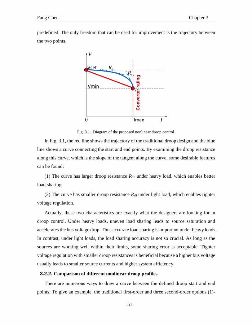
Fang Chen Chapter 3
-51-
predefined. The only freedom that can be used for improvement is the trajectory between
the two points.
Fig. 3.1. Diagram of the proposed nonlinear droop control.
In Fig. 3.1, the red line shows the trajectory of the traditional droop design and the blue
line shows a curve connecting the start and end points. By examining the droop resistance
along this curve, which is the slope of the tangent along the curve, some desirable features
can be found:
(1) The curve has larger droop resistance Rd2 under heavy load, which enables better
load sharing.
(2) The curve has smaller droop resistance Rd1 under light load, which enables tighter
voltage regulation.
Actually, these two characteristics are exactly what the designers are looking for in
droop control. Under heavy loads, uneven load sharing leads to source saturation and
accelerates the bus voltage drop. Thus accurate load sharing is important under heavy loads.
In contrast, under light loads, the load sharing accuracy is not so crucial. As long as the
sources are working well within their limits, some sharing error is acceptable. Tighter
voltage regulation with smaller droop resistances is beneficial because a higher bus voltage
usually leads to smaller source currents and higher system efficiency.
3.2.2. Comparison of different nonlinear droop profiles
There are numerous ways to draw a curve between the defined droop start and end
points. To give an example, the traditional first-order and three second-order options (1)-
0 I
Vset
Vmin
V
Imax
Co
nve
rte
r ra
tin
g
1dR
2dR
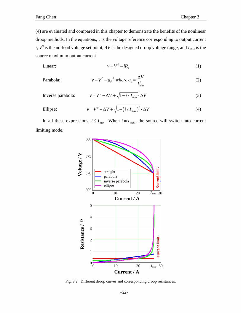
Fang Chen Chapter 3
-52-
(4) are evaluated and compared in this chapter to demonstrate the benefits of the nonlinear
droop methods. In the equations, v is the voltage reference corresponding to output current
i, V0 is the no-load voltage set point, ΔV is the designed droop voltage range, and Imax is the
source maximum output current.
Linear: 0
dv V iR (1)
Parabola: 0 2
1v V a i 1 2
max
Vwhere a
I
(2)
Inverse parabola: 0
max1 /v V V i I V (3)
Ellipse: 20
max1 /v V V i I V (4)
In all these expressions, maxi I . When
maxi I , the source will switch into current
limiting mode.
0
1
2
3
4
5
Current / A
Res
ista
nce
/ Ω
Cu
rre
nt
limit
Imax0 10 20 30
365
370
375
380
straight
parabola
inverse parabolaellipse
Current / A
Imax
Cu
rre
nt
limit
Volt
age
/ V
0 10 20 30
Fig. 3.2. Different droop curves and corresponding droop resistances.

Fang Chen Chapter 3
-53-
In Fig. 3.2, three different droop trajectories and their droop resistances are plotted
against the traditional straight-line droop. Their droop resistances at no load and full load
are summarized in Table 3.1. In this example, the bus voltage range is chosen as 370 V to
380 V, the source rating is 10 kW, and the maximum output current at 370 V is around
27 A. It can be observed that the traditional linear droop has a fixed droop resistance for
the whole load range. The parabola has zero slope under no-load condition. This means
that under very light-load conditions, the line resistance determines how the load is shared
among multiple sources. Under full-load conditions, the droop resistance of the parabola is
limited. The value is bigger than the constant output resistance of the traditional linear
droop, but still not infinite. The inverse parabola and ellipse both have infinite droop
resistance under full load, which theoretically can eliminate the impact from cables. The
transition between voltage regulation mode and current limiting mode is also smooth in
inverse parabola and ellipse droop methods because there is no abrupt slope change. The
difference between the two droop methods is that the ellipse has zero resistance at no load
while the inverse parabola has some limited value.
Table 3.1. Comparison and evaluation of different droops.
Type No-load droop
resistance
Full-load droop
resistance
Metrics
Linear Fixed Fixed X
Parabola 0 Limted X
Inverse Parabola Limited ∞ √
Ellipse 0 ∞ √
3.2.3. Performance comparison between linear and nonlinear droops
Fig. 3.3 and Fig. 3.4 present the schematic and time domain simulation results between
the traditional droop and the inverse parabola droop methods. Two sources are paralleled
to a bus to provide power to a load. Some cable resistance is inserted between Source 2
and the load. As the analysis implies, the inverse parabola droop method has relatively
larger current unbalance under light load but better load sharing under heavy load. In
addition, the necessary droop voltage range to fully utilize the sources’ capability is smaller.
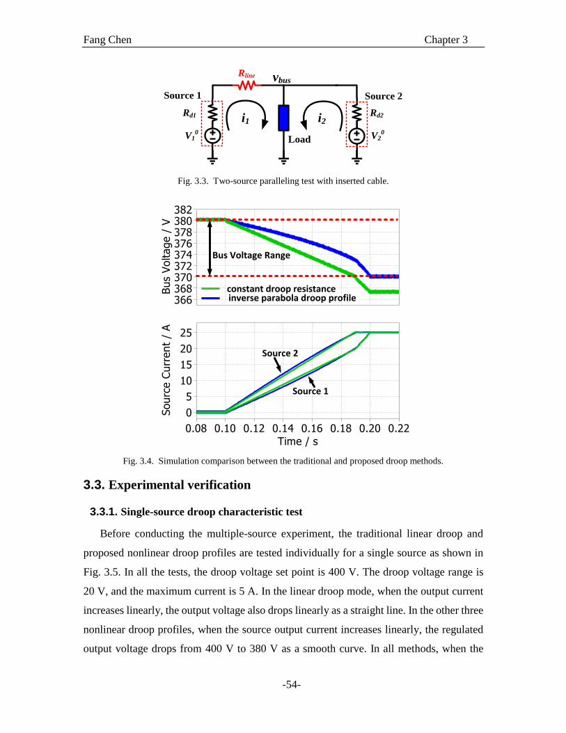
Fang Chen Chapter 3
-54-
LoadV10
i1 i2Rd1 Rd2
vbus
Source 1 Source 2
V20
Rline
Fig. 3.3. Two-source paralleling test with inserted cable.
Bus Voltage Range
constant droop resistanceinverse parabola droop profile
Source 2
Source 1
Fig. 3.4. Simulation comparison between the traditional and proposed droop methods.
3.3. Experimental verification
3.3.1. Single-source droop characteristic test
Before conducting the multiple-source experiment, the traditional linear droop and
proposed nonlinear droop profiles are tested individually for a single source as shown in
Fig. 3.5. In all the tests, the droop voltage set point is 400 V. The droop voltage range is
20 V, and the maximum current is 5 A. In the linear droop mode, when the output current
increases linearly, the output voltage also drops linearly as a straight line. In the other three
nonlinear droop profiles, when the source output current increases linearly, the regulated
output voltage drops from 400 V to 380 V as a smooth curve. In all methods, when the
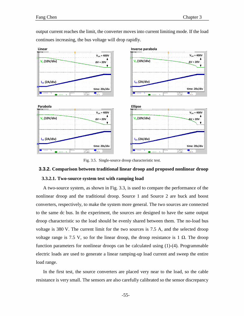
Fang Chen Chapter 3
-55-
output current reaches the limit, the converter moves into current limiting mode. If the load
continues increasing, the bus voltage will drop rapidly.
Vo (10V/div)
Io1 (2A/div)
Vset = 400V
time: 20s/div
V = 20V
Linear Inverse parabola
Parabola Ellipse
Vo (10V/div)
Io1 (2A/div)
Vset = 400V
time: 20s/div
V = 20V
Vo (10V/div)
Io1 (2A/div)
Vset = 400V
time: 20s/div
V = 20V Vo (10V/div)
Io1 (2A/div)
Vset = 400V
time: 20s/div
V = 20V
Fig. 3.5. Single-source droop characteristic test.
3.3.2. Comparison between traditional linear droop and proposed nonlinear droop
3.3.2.1. Two-source system test with ramping load
A two-source system, as shown in Fig. 3.3, is used to compare the performance of the
nonlinear droop and the traditional droop. Source 1 and Source 2 are buck and boost
converters, respectively, to make the system more general. The two sources are connected
to the same dc bus. In the experiment, the sources are designed to have the same output
droop characteristic so the load should be evenly shared between them. The no-load bus
voltage is 380 V. The current limit for the two sources is 7.5 A, and the selected droop
voltage range is 7.5 V, so for the linear droop, the droop resistance is 1 Ω. The droop
function parameters for nonlinear droops can be calculated using (1)-(4). Programmable
electric loads are used to generate a linear ramping-up load current and sweep the entire
load range.
In the first test, the source converters are placed very near to the load, so the cable
resistance is very small. The sensors are also carefully calibrated so the sensor discrepancy
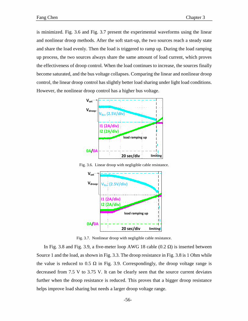
Fang Chen Chapter 3
-56-
is minimized. Fig. 3.6 and Fig. 3.7 present the experimental waveforms using the linear
and nonlinear droop methods. After the soft start-up, the two sources reach a steady state
and share the load evenly. Then the load is triggered to ramp up. During the load ramping
up process, the two sources always share the same amount of load current, which proves
the effectiveness of droop control. When the load continues to increase, the sources finally
become saturated, and the bus voltage collapses. Comparing the linear and nonlinear droop
control, the linear droop control has slightly better load sharing under light load conditions.
However, the nonlinear droop control has a higher bus voltage.
VBus (2.5V/div)
I2 (2A/div)
Vset
limiting20 sec/div
I1 (2A/div)
load ramping up
0A/0A
Vdroop
Fig. 3.6. Linear droop with negligible cable resistance.
VBus (2.5V/div)
I2 (2A/div)
Vset
0A/0A20 sec/div
I1 (2A/div)
load ramping up
limiting
Vdroop
Fig. 3.7. Nonlinear droop with negligible cable resistance.
In Fig. 3.8 and Fig. 3.9, a five-meter loop AWG 18 cable (0.2 Ω) is inserted between
Source 1 and the load, as shown in Fig. 3.3. The droop resistance in Fig. 3.8 is 1 Ohm while
the value is reduced to 0.5 Ω in Fig. 3.9. Correspondingly, the droop voltage range is
decreased from 7.5 V to 3.75 V. It can be clearly seen that the source current deviates
further when the droop resistance is reduced. This proves that a bigger droop resistance
helps improve load sharing but needs a larger droop voltage range.
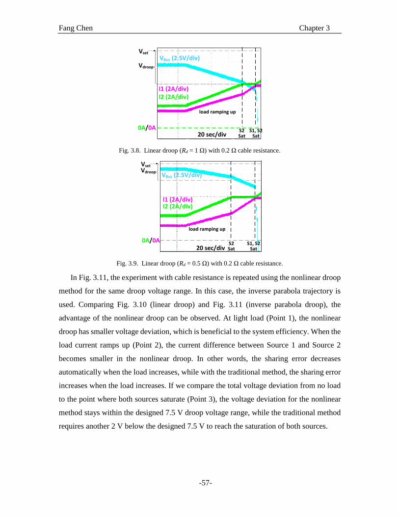
Fang Chen Chapter 3
-57-
VBus (2.5V/div)
I2 (2A/div)
20 sec/div
I1 (2A/div)
load ramping up
S2Sat
S1, S2Sat
0A/0A
Vset
Vdroop
Fig. 3.8. Linear droop (Rd = 1 Ω) with 0.2 Ω cable resistance.
VBus (2.5V/div)
I2 (2A/div)
20 sec/div
I1 (2A/div)
load ramping up
S2Sat
S1, S2Sat
0A/0A
VsetVdroop
Fig. 3.9. Linear droop (Rd = 0.5 Ω) with 0.2 Ω cable resistance.
In Fig. 3.11, the experiment with cable resistance is repeated using the nonlinear droop
method for the same droop voltage range. In this case, the inverse parabola trajectory is
used. Comparing Fig. 3.10 (linear droop) and Fig. 3.11 (inverse parabola droop), the
advantage of the nonlinear droop can be observed. At light load (Point 1), the nonlinear
droop has smaller voltage deviation, which is beneficial to the system efficiency. When the
load current ramps up (Point 2), the current difference between Source 1 and Source 2
becomes smaller in the nonlinear droop. In other words, the sharing error decreases
automatically when the load increases, while with the traditional method, the sharing error
increases when the load increases. If we compare the total voltage deviation from no load
to the point where both sources saturate (Point 3), the voltage deviation for the nonlinear
method stays within the designed 7.5 V droop voltage range, while the traditional method
requires another 2 V below the designed 7.5 V to reach the saturation of both sources.
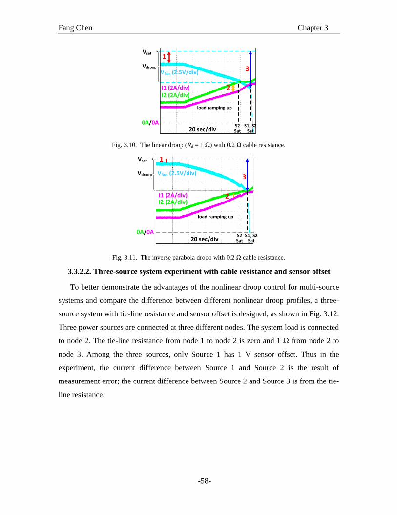
Fang Chen Chapter 3
-58-
VBus (2.5V/div)
I2 (2A/div)
Vset
0A/0A20 sec/div
I1 (2A/div)
load ramping up
S2Sat
S1, S2Sat
1
2
3Vdroop
Fig. 3.10. The linear droop (Rd = 1 Ω) with 0.2 Ω cable resistance.
VBus (2.5V/div)
I2 (2A/div)
Vset
0A/0A20 sec/div
I1 (2A/div)
S2Sat
S1, S2Sat
1
2
3
load ramping up
Vdroop
Fig. 3.11. The inverse parabola droop with 0.2 Ω cable resistance.
3.3.2.2. Three-source system experiment with cable resistance and sensor offset
To better demonstrate the advantages of the nonlinear droop control for multi-source
systems and compare the difference between different nonlinear droop profiles, a three-
source system with tie-line resistance and sensor offset is designed, as shown in Fig. 3.12.
Three power sources are connected at three different nodes. The system load is connected
to node 2. The tie-line resistance from node 1 to node 2 is zero and 1 Ω from node 2 to
node 3. Among the three sources, only Source 1 has 1 V sensor offset. Thus in the
experiment, the current difference between Source 1 and Source 2 is the result of
measurement error; the current difference between Source 2 and Source 3 is from the tie-
line resistance.
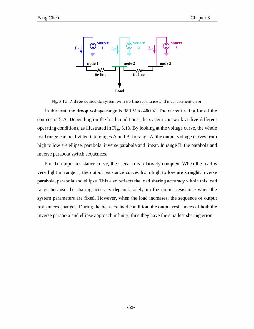
Fang Chen Chapter 3
-59-
node 1 node 2 node 3
tie line tie line
Load
Is1 Is2 Is3
Source
1
Source
2
Source
3
Fig. 3.12. A three-source dc system with tie-line resistance and measurement error.
In this test, the droop voltage range is 380 V to 400 V. The current rating for all the
sources is 5 A. Depending on the load conditions, the system can work at five different
operating conditions, as illustrated in Fig. 3.13. By looking at the voltage curve, the whole
load range can be divided into ranges A and B. In range A, the output voltage curves from
high to low are ellipse, parabola, inverse parabola and linear. In range B, the parabola and
inverse parabola switch sequences.
For the output resistance curve, the scenario is relatively complex. When the load is
very light in range 1, the output resistance curves from high to low are straight, inverse
parabola, parabola and ellipse. This also reflects the load sharing accuracy within this load
range because the sharing accuracy depends solely on the output resistance when the
system parameters are fixed. However, when the load increases, the sequence of output
resistances changes. During the heaviest load condition, the output resistances of both the
inverse parabola and ellipse approach infinity; thus they have the smallest sharing error.
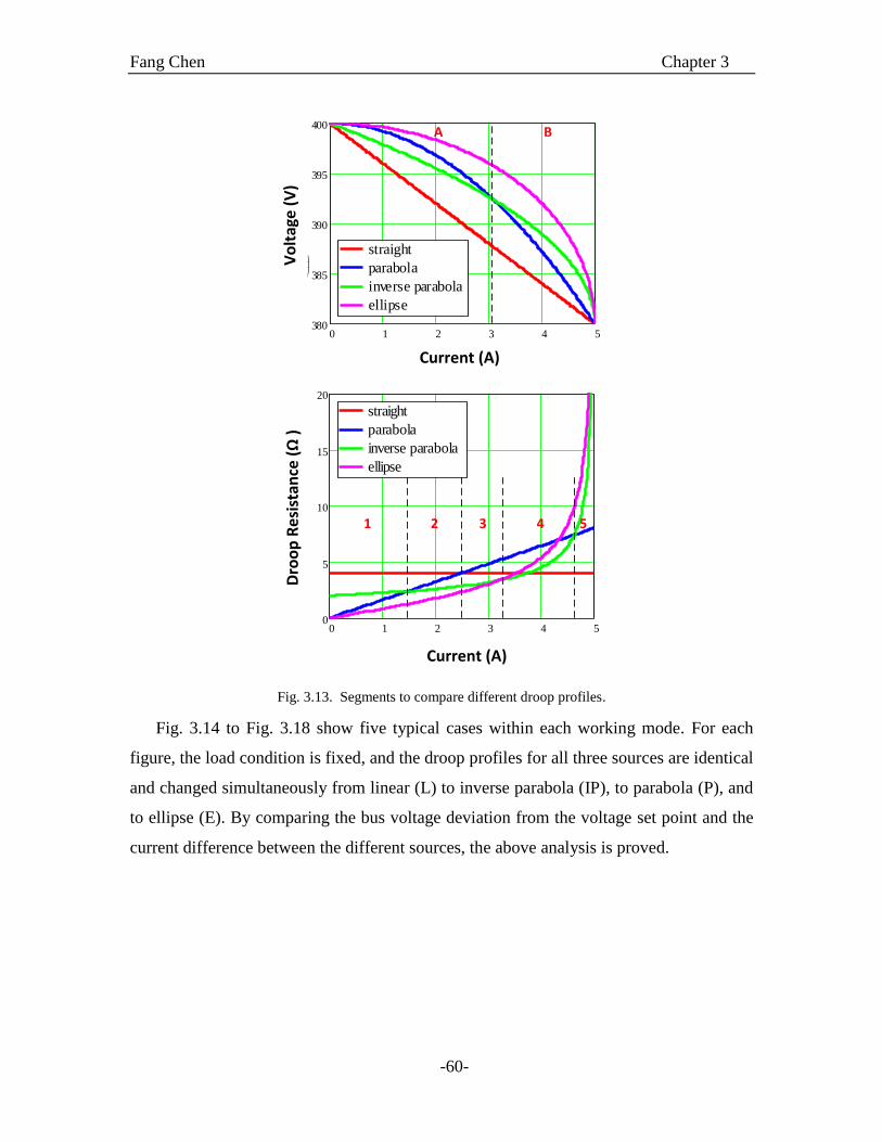
Fang Chen Chapter 3
-60-
0 1 2 3 4 50
5
10
15
20
straight
parabola
inverse parabola
ellipse
x400 4x( )
d
d
x400 0.8 x
2 d
d
x380 20 1 0.2 x d
d
x380 20 1
x
5
2
d
d
xCurrent (A)
Dro
op
Re
sist
ance
( )
0 1 2 3 4 5380
385
390
395
400
straight
parabola
inverse parabola
ellipse
400 4x
400 0.8 x2
380 20 1 0.2 x
380 20 1x
5
2
xCurrent (A)
Vo
ltag
e (
V)
1 2 3 4 5
A B
Fig. 3.13. Segments to compare different droop profiles.
Fig. 3.14 to Fig. 3.18 show five typical cases within each working mode. For each
figure, the load condition is fixed, and the droop profiles for all three sources are identical
and changed simultaneously from linear (L) to inverse parabola (IP), to parabola (P), and
to ellipse (E). By comparing the bus voltage deviation from the voltage set point and the
current difference between the different sources, the above analysis is proved.
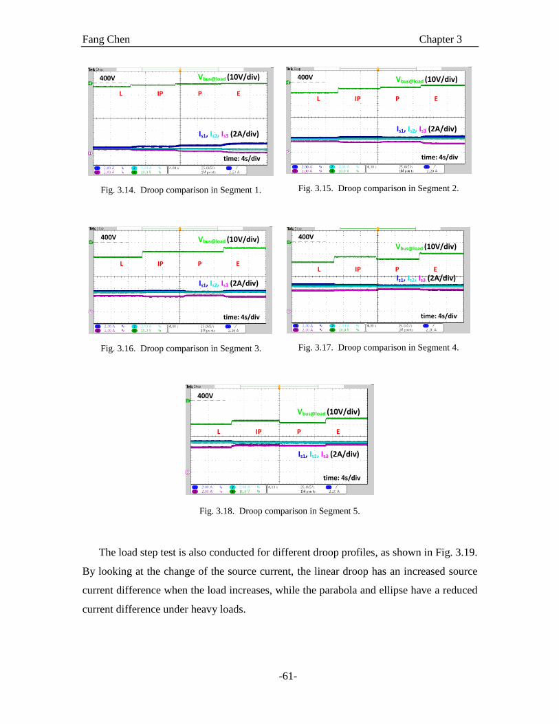
Fang Chen Chapter 3
-61-
Vbus@load (10V/div)
Is1, Is2, Is3 (2A/div)
L IP P E
time: 4s/div
400V
Fig. 3.14. Droop comparison in Segment 1.
Vbus@load (10V/div)
Is1, Is2, Is3 (2A/div)
time: 4s/div
400V
L IP P E
Fig. 3.15. Droop comparison in Segment 2.
Vbus@load (10V/div)
Is1, Is2, Is3 (2A/div)
time: 4s/div
400V
L IP P E
Fig. 3.16. Droop comparison in Segment 3.
Vbus@load (10V/div)
Is1, Is2, Is3 (2A/div)
time: 4s/div
400V
L IP P E
Fig. 3.17. Droop comparison in Segment 4.
Vbus@load (10V/div)
Is1, Is2, Is3 (2A/div)
time: 4s/div
400V
L IP P E
Fig. 3.18. Droop comparison in Segment 5.
The load step test is also conducted for different droop profiles, as shown in Fig. 3.19.
By looking at the change of the source current, the linear droop has an increased source
current difference when the load increases, while the parabola and ellipse have a reduced
current difference under heavy loads.
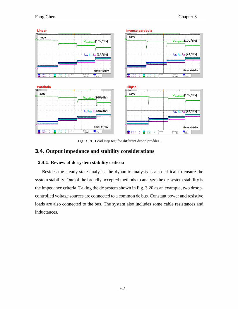
Fang Chen Chapter 3
-62-
Vbus@load (10V/div)
Is1, Is2, Is3 (2A/div)
time: 4s/div
400VVbus@load (10V/div)
Is1, Is2, Is3 (2A/div)
time: 4s/div
400V
Vbus@load (10V/div)
Is1, Is2, Is3 (2A/div)
time: 4s/div
400V Vbus@load (10V/div)
Is1, Is2, Is3 (2A/div)
time: 4s/div
400V
Linear Inverse parabola
Parabola Ellipse
Fig. 3.19. Load step test for different droop profiles.
3.4. Output impedance and stability considerations
3.4.1. Review of dc system stability criteria
Besides the steady-state analysis, the dynamic analysis is also critical to ensure the
system stability. One of the broadly accepted methods to analyze the dc system stability is
the impedance criteria. Taking the dc system shown in Fig. 3.20 as an example, two droop-
controlled voltage sources are connected to a common dc bus. Constant power and resistive
loads are also connected to the bus. The system also includes some cable resistances and
inductances.
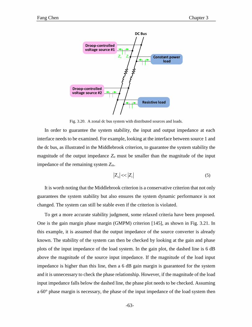
Fang Chen Chapter 3
-63-
Fig. 3.20. A zonal dc bus system with distributed sources and loads.
In order to guarantee the system stability, the input and output impedance at each
interface needs to be examined. For example, looking at the interface between source 1 and
the dc bus, as illustrated in the Middlebrook criterion, to guarantee the system stability the
magnitude of the output impedance Zo must be smaller than the magnitude of the input
impedance of the remaining system Zin.
Zo iZ (5)
It is worth noting that the Middlebrook criterion is a conservative criterion that not only
guarantees the system stability but also ensures the system dynamic performance is not
changed. The system can still be stable even if the criterion is violated.
To get a more accurate stability judgment, some relaxed criteria have been proposed.
One is the gain margin phase margin (GMPM) criterion [145], as shown in Fig. 3.21. In
this example, it is assumed that the output impedance of the source converter is already
known. The stability of the system can then be checked by looking at the gain and phase
plots of the input impedance of the load system. In the gain plot, the dashed line is 6 dB
above the magnitude of the source input impedance. If the magnitude of the load input
impedance is higher than this line, then a 6 dB gain margin is guaranteed for the system
and it is unnecessary to check the phase relationship. However, if the magnitude of the load
input impedance falls below the dashed line, the phase plot needs to be checked. Assuming
a 60° phase margin is necessary, the phase of the input impedance of the load system then
DC Bus
Droop-controlledvoltage source #1
Constant powerload
Droop-controlledvoltage source #2
Resistive load
Zo Zi
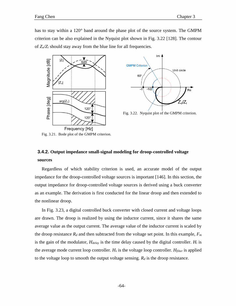
Fang Chen Chapter 3
-64-
has to stay within a 120° band around the phase plot of the source system. The GMPM
criterion can be also explained in the Nyquist plot shown in Fig. 3.22 [128]. The contour
of Zo/Zi should stay away from the blue line for all frequencies.
Fig. 3.21. Bode plot of the GMPM criterion.
Fig. 3.22. Nyquist plot of the GMPM criterion.
3.4.2. Output impedance small-signal modeling for droop-controlled voltage
sources
Regardless of which stability criterion is used, an accurate model of the output
impedance for the droop-controlled voltage sources is important [146]. In this section, the
output impedance for droop-controlled voltage sources is derived using a buck converter
as an example. The derivation is first conducted for the linear droop and then extended to
the nonlinear droop.
In Fig. 3.23, a digital controlled buck converter with closed current and voltage loops
are drawn. The droop is realized by using the inductor current, since it shares the same
average value as the output current. The average value of the inductor current is scaled by
the droop resistance Rd and then subtracted from the voltage set point. In this example, Fm
is the gain of the modulator, Hdelay is the time delay caused by the digital controller. Hi is
the average mode current loop controller. Hv is the voltage loop controller. Hfilter is applied
to the voltage loop to smooth the output voltage sensing. Rd is the droop resistance.
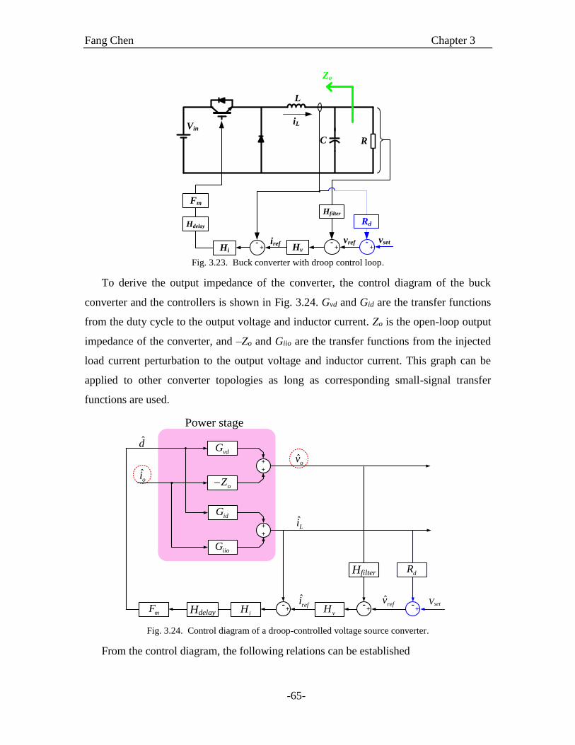
Fang Chen Chapter 3
-65-
iL
L
Vin
C R
Zo
HvHi
Rd
-+
-+
-+
Hfilter
vsetvrefiref
Fm
Hdelay
Fig. 3.23. Buck converter with droop control loop.
To derive the output impedance of the converter, the control diagram of the buck
converter and the controllers is shown in Fig. 3.24. Gvd and Gid are the transfer functions
from the duty cycle to the output voltage and inductor current. Zo is the open-loop output
impedance of the converter, and –Zo and Giio are the transfer functions from the injected
load current perturbation to the output voltage and inductor current. This graph can be
applied to other converter topologies as long as corresponding small-signal transfer
functions are used.
+
+
+
+
ˆoi
d
ˆov
ˆLi
vdG
idG
oZ
iioG
-+
vH-
+iHmF -
+
dR
ˆrefvˆ
refi
Power stage
Hfilter
Hdelay
Vset
Fig. 3.24. Control diagram of a droop-controlled voltage source converter.
From the control diagram, the following relations can be established
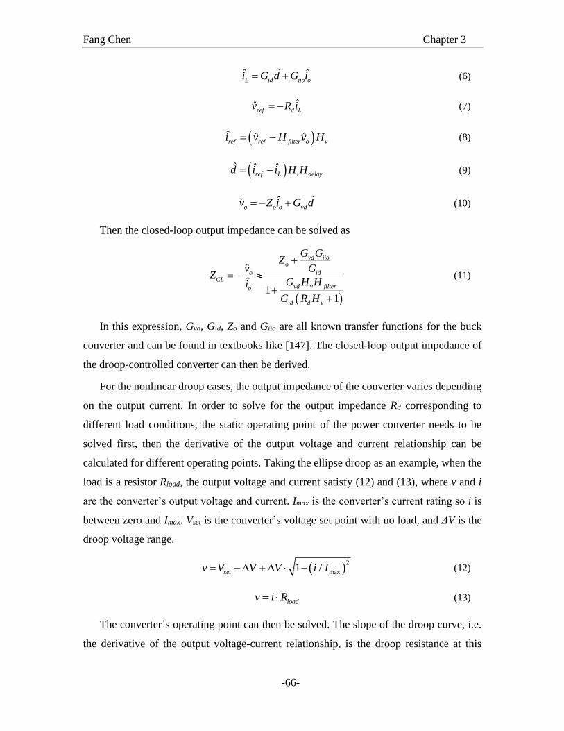
Fang Chen Chapter 3
-66-
ˆˆ ˆL id iio oi G d G i (6)
ˆˆref d Lv R i (7)
ˆ ˆ ˆref ref filter o vi v H v H (8)
ˆ ˆ ˆref L i delayd i i H H (9)
ˆˆˆo o o vdv Z i G d (10)
Then the closed-loop output impedance can be solved as
ˆ
ˆ1
1
vd iioo
o idCL
vd v filtero
id d v
G GZ
v GZ
G H Hi
G R H
(11)
In this expression, Gvd, Gid, Zo and Giio are all known transfer functions for the buck
converter and can be found in textbooks like [147]. The closed-loop output impedance of
the droop-controlled converter can then be derived.
For the nonlinear droop cases, the output impedance of the converter varies depending
on the output current. In order to solve for the output impedance Rd corresponding to
different load conditions, the static operating point of the power converter needs to be
solved first, then the derivative of the output voltage and current relationship can be
calculated for different operating points. Taking the ellipse droop as an example, when the
load is a resistor Rload, the output voltage and current satisfy (12) and (13), where v and i
are the converter’s output voltage and current. Imax is the converter’s current rating so i is
between zero and Imax. Vset is the converter’s voltage set point with no load, and ΔV is the
droop voltage range.
2
max1 /setv V V V i I (12)
loadv i R (13)
The converter’s operating point can then be solved. The slope of the droop curve, i.e.
the derivative of the output voltage-current relationship, is the droop resistance at this
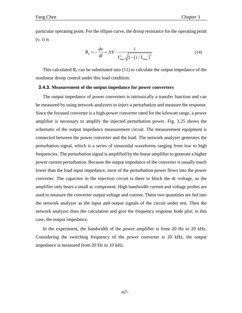
Fang Chen Chapter 3
-67-
particular operating point. For the ellipse curve, the droop resistance for the operating point
(v, i) is
22
max max1 /d
dv iR V
di I i I
(14)
This calculated Rd can be substituted into (11) to calculate the output impedance of the
nonlinear droop control under this load condition.
3.4.3. Measurement of the output impedance for power converters
The output impedance of power converters is intrinsically a transfer function and can
be measured by using network analyzers to inject a perturbation and measure the response.
Since the focused converter is a high-power converter rated for the kilowatt range, a power
amplifier is necessary to amplify the injected perturbation power. Fig. 3.25 shows the
schematic of the output impedance measurement circuit. The measurement equipment is
connected between the power converter and the load. The network analyzer generates the
perturbation signal, which is a series of sinusoidal waveforms ranging from low to high
frequencies. The perturbation signal is amplified by the linear amplifier to generate a higher
power current perturbation. Because the output impedance of the converter is usually much
lower than the load input impedance, most of the perturbation power flows into the power
converter. The capacitor in the injection circuit is there to block the dc voltage, so the
amplifier only bears a small ac component. High bandwidth current and voltage probes are
used to measure the converter output voltage and current. These two quantities are fed into
the network analyzer as the input and output signals of the circuit under test. Then the
network analyzer does the calculation and give the frequency response bode plot; in this
case, the output impedance.
In the experiment, the bandwidth of the power amplifier is from 20 Hz to 20 kHz.
Considering the switching frequency of the power converter is 20 kHz, the output
impedance is measured from 20 Hz to 10 kHz.
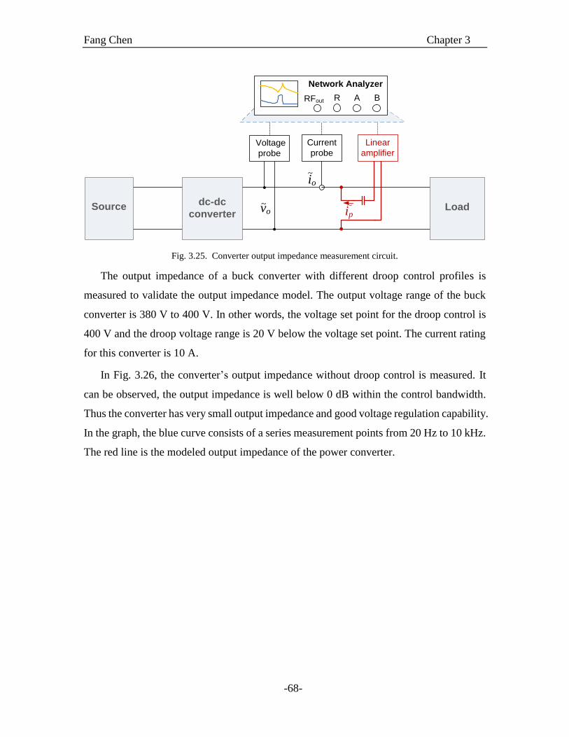
Fang Chen Chapter 3
-68-
Vo
Zs
YLdc-dc
converterSource Loadvo
~
Voltage
probe
Current
probe
io~
ip~
Linear
amplifier
RFout R A B
Network Analyzer
Fig. 3.25. Converter output impedance measurement circuit.
The output impedance of a buck converter with different droop control profiles is
measured to validate the output impedance model. The output voltage range of the buck
converter is 380 V to 400 V. In other words, the voltage set point for the droop control is
400 V and the droop voltage range is 20 V below the voltage set point. The current rating
for this converter is 10 A.
In Fig. 3.26, the converter’s output impedance without droop control is measured. It
can be observed, the output impedance is well below 0 dB within the control bandwidth.
Thus the converter has very small output impedance and good voltage regulation capability.
In the graph, the blue curve consists of a series measurement points from 20 Hz to 10 kHz.
The red line is the modeled output impedance of the power converter.
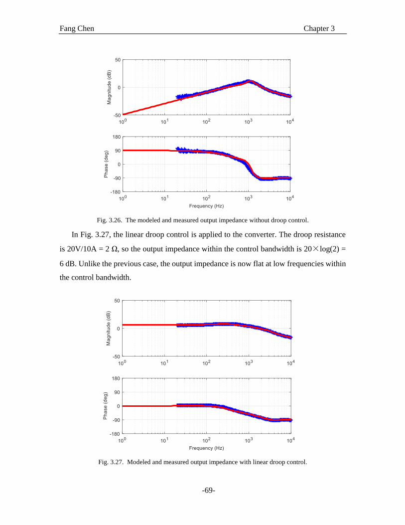
Fang Chen Chapter 3
-69-
Fig. 3.26. The modeled and measured output impedance without droop control.
In Fig. 3.27, the linear droop control is applied to the converter. The droop resistance
is 20V/10A = 2 Ω, so the output impedance within the control bandwidth is 20×log(2) =
6 dB. Unlike the previous case, the output impedance is now flat at low frequencies within
the control bandwidth.
Fig. 3.27. Modeled and measured output impedance with linear droop control.
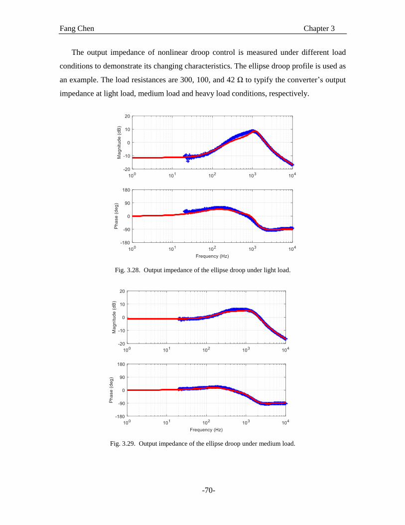
Fang Chen Chapter 3
-70-
The output impedance of nonlinear droop control is measured under different load
conditions to demonstrate its changing characteristics. The ellipse droop profile is used as
an example. The load resistances are 300, 100, and 42 Ω to typify the converter’s output
impedance at light load, medium load and heavy load conditions, respectively.
Fig. 3.28. Output impedance of the ellipse droop under light load.
Fig. 3.29. Output impedance of the ellipse droop under medium load.
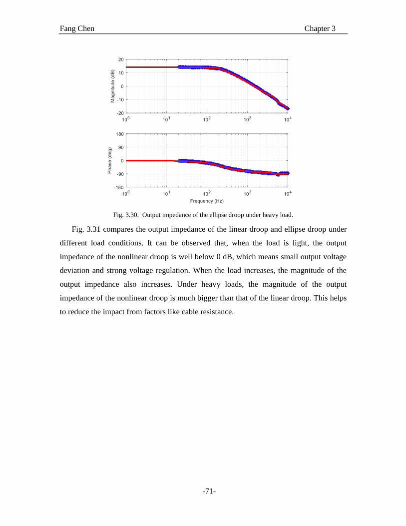
Fang Chen Chapter 3
-71-
Fig. 3.30. Output impedance of the ellipse droop under heavy load.
Fig. 3.31 compares the output impedance of the linear droop and ellipse droop under
different load conditions. It can be observed that, when the load is light, the output
impedance of the nonlinear droop is well below 0 dB, which means small output voltage
deviation and strong voltage regulation. When the load increases, the magnitude of the
output impedance also increases. Under heavy loads, the magnitude of the output
impedance of the nonlinear droop is much bigger than that of the linear droop. This helps
to reduce the impact from factors like cable resistance.
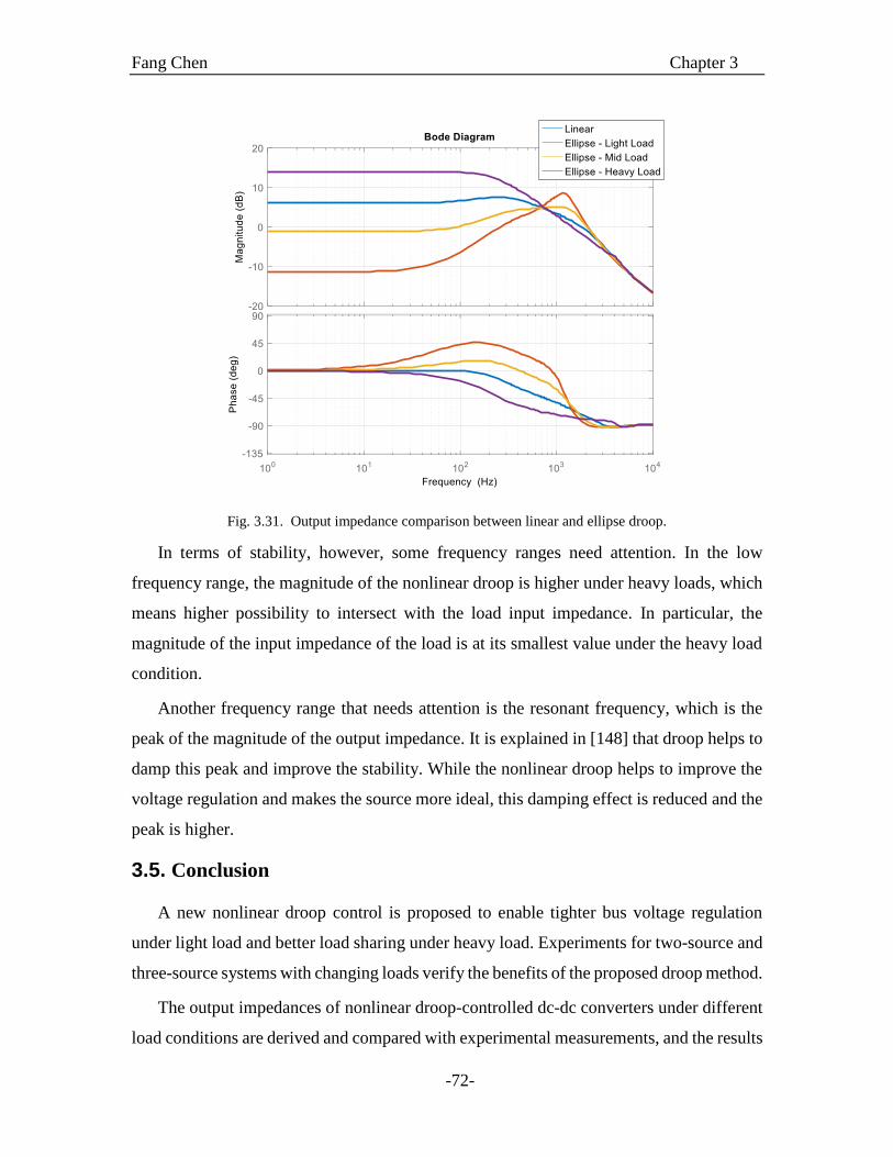
Fang Chen Chapter 3
-72-
Fig. 3.31. Output impedance comparison between linear and ellipse droop.
In terms of stability, however, some frequency ranges need attention. In the low
frequency range, the magnitude of the nonlinear droop is higher under heavy loads, which
means higher possibility to intersect with the load input impedance. In particular, the
magnitude of the input impedance of the load is at its smallest value under the heavy load
condition.
Another frequency range that needs attention is the resonant frequency, which is the
peak of the magnitude of the output impedance. It is explained in [148] that droop helps to
damp this peak and improve the stability. While the nonlinear droop helps to improve the
voltage regulation and makes the source more ideal, this damping effect is reduced and the
peak is higher.
3.5. Conclusion
A new nonlinear droop control is proposed to enable tighter bus voltage regulation
under light load and better load sharing under heavy load. Experiments for two-source and
three-source systems with changing loads verify the benefits of the proposed droop method.
The output impedances of nonlinear droop-controlled dc-dc converters under different
load conditions are derived and compared with experimental measurements, and the results

Fang Chen Chapter 3
-73-
match well. While improving the static performance, the nonlinear droop control increases
the magnitude of the output impedance in certain frequency ranges. This needs to be
considered when evaluating the system stability.

Fang Chen Chapter 4
-74-
Chapter 4. DC SYSTEM POWER FLOW ANALYSIS AND
PERFORMANCE IMPROVEMENT USING NEAREST-NODE
COMMUNICATION
The dc microgrid has attained popularity for integrating renewable energy sources and
batteries. It also has the potential to achieve higher efficiency than the ac power grid. In
this chapter, a generic dc microgrid is modeled based on a cluster of generic dc nodes,
which include constant power generation by renewables, droop-controlled voltage sources,
and different kinds of loads. The static dc power flow is solved. A voltage restoration
method based on nearest-node communication is used to restore the voltage deviation
caused by droop characteristics. An enhanced current regulator guarantees accurate load
sharing even under the influence of sensor drift and line resistance. A tie-line power flow
control method is proposed to regulate the tie-line power and increase the system efficiency
under light-load conditions. All of the considered methods only need the local information
and the information from its neighbor; hence the system expendability is guaranteed.
Simulation and experimental results are provided to validate the proposed methods.
4.1. Review of microgrid control strategies with communication links
DC microgrids are increasingly gaining attention because of the simplicity in
integrating different renewable sources and energy storage devices, no need for
synchronization, and the possibility to achieve higher efficiency than ac grids [3]. Droop
control is broadly used to coordinate multiple sources paralleled to a common bus in dc
grids. By introducing a virtual output resistance to each source, the circulating current is
suppressed and load sharing among sources is realized.
To better predict the power flow and load sharing in dc systems, some dc system models
have been discussed in [71], [149]–[153]; however, the systems in these works are either
too small or too simplified. In a practical system, the loads can be constant resistance,
constant power or constant current. The sources can also have different characteristics. A
generic dc system model is necessary to predict the system power flow and voltage
distribution.
Fang Chen Chapter 4
-75-
Besides voltage regulation and current sharing, droop control has been also discussed
from other perspectives. A cost-based droop strategy is discussed in [154] to reduce the
operation cost. Dynamic load sharing is considered in [155]–[158], in which the load
dynamic is dispatched to different sources, i.e. supercapacitors for high-frequency load
power and batteries for low-frequency load power. Efficiency optimization by changing
the droop parameters is discussed in [159]–[163]. Harmonic sharing is discussed in [164].
In [165], the State-of-Charge (SoC) of batteries is monitored to adjust the droop parameters
online so that the SoC of different batteries can be balanced.
Though the droop principle has been used in many applications, it is still unclear how
to analyze and optimize the power flow in dc grids that include a variety of different kinds
of power nodes. In [149], the steady-state performance and sensitivity of dc microgrids are
analyzed, but only droop-controlled voltage sources and constant current loads are
considered. In [138], the design of the droop voltage range and the cable’s impact on dc
system performance are analyzed quantitatively, but the analyzed system is small and has
a limited number of nodes. In [71]–[74], different secondary-control methods are proposed
to restore the dc bus voltage deviation from droop control and ensure a proportional load
sharing. However, all these methods rely on dedicated communication links, which reduce
the system reliability and expandability. Furthermore, though these methods reduce the
steady-state bus voltage deviation and make the load sharing proportional to the source
ratings, the outcome and benefits of these improvements are still unclear. In [163], a
hierarchical control structure is used to optimize the efficiency of dc microgrids. It is
reported that uneven load sharing is more efficient under light-load conditions, while
proportional load sharing is more efficient under heavy load. However, the discussed
algorithm is very complicated, and is only demonstrated for a two-source system where the
source efficiency curves are known.
To save the communication links in distributed control, a consensus-based control
method is introduced to the field of microgrids from multi-agent systems in [78]–[80], [83].
This method enables bus voltage restoration and load sharing with communication between
only adjacent nodes. This also makes it possible to achieve system optimization without
complicated communication networks.
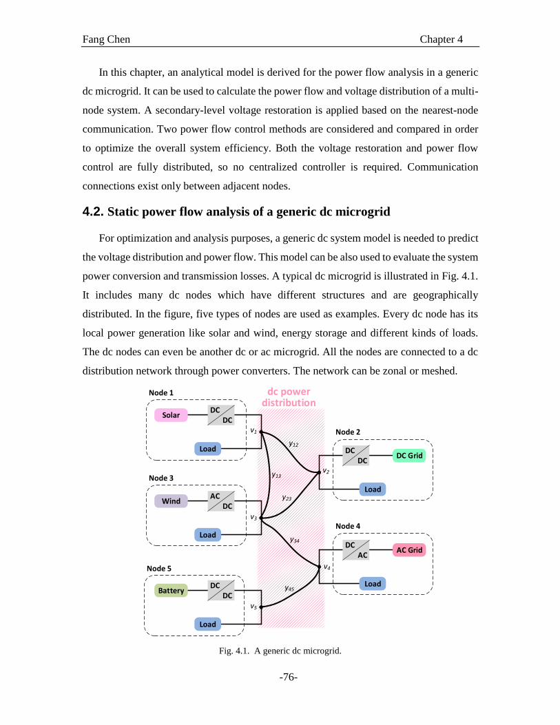
Fang Chen Chapter 4
-76-
In this chapter, an analytical model is derived for the power flow analysis in a generic
dc microgrid. It can be used to calculate the power flow and voltage distribution of a multi-
node system. A secondary-level voltage restoration is applied based on the nearest-node
communication. Two power flow control methods are considered and compared in order
to optimize the overall system efficiency. Both the voltage restoration and power flow
control are fully distributed, so no centralized controller is required. Communication
connections exist only between adjacent nodes.
4.2. Static power flow analysis of a generic dc microgrid
For optimization and analysis purposes, a generic dc system model is needed to predict
the voltage distribution and power flow. This model can be also used to evaluate the system
power conversion and transmission losses. A typical dc microgrid is illustrated in Fig. 4.1.
It includes many dc nodes which have different structures and are geographically
distributed. In the figure, five types of nodes are used as examples. Every dc node has its
local power generation like solar and wind, energy storage and different kinds of loads.
The dc nodes can even be another dc or ac microgrid. All the nodes are connected to a dc
distribution network through power converters. The network can be zonal or meshed.
Node 4
Node 5
Node 3
DCDC
Solar
Load
ACDC
Wind
Load
DCDC
Battery
Load
DCDC
DC Grid
Load
DCAC
AC Grid
Load
Node 1
Node 2
y12
y23
y34
y45
v2
v1
v3
v4
v5
y13
dc power distribution
Fig. 4.1. A generic dc microgrid.
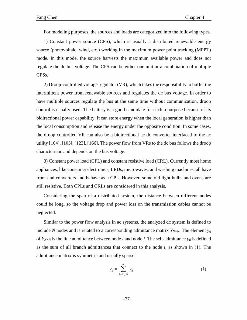
Fang Chen Chapter 4
-77-
For modeling purposes, the sources and loads are categorized into the following types.
1) Constant power source (CPS), which is usually a distributed renewable energy
source (photovoltaic, wind, etc.) working in the maximum power point tracking (MPPT)
mode. In this mode, the source harvests the maximum available power and does not
regulate the dc bus voltage. The CPS can be either one unit or a combination of multiple
CPSs.
2) Droop-controlled voltage regulator (VR), which takes the responsibility to buffer the
intermittent power from renewable sources and regulates the dc bus voltage. In order to
have multiple sources regulate the bus at the same time without communication, droop
control is usually used. The battery is a good candidate for such a purpose because of its
bidirectional power capability. It can store energy when the local generation is higher than
the local consumption and release the energy under the opposite condition. In some cases,
the droop-controlled VR can also be a bidirectional ac-dc converter interfaced to the ac
utility [104], [105], [123], [166]. The power flow from VRs to the dc bus follows the droop
characteristic and depends on the bus voltage.
3) Constant power load (CPL) and constant resistive load (CRL). Currently most home
appliances, like consumer electronics, LEDs, microwaves, and washing machines, all have
front-end converters and behave as a CPL. However, some old light bulbs and ovens are
still resistive. Both CPLs and CRLs are considered in this analysis.
Considering the span of a distributed system, the distance between different nodes
could be long, so the voltage drop and power loss on the transmission cables cannot be
neglected.
Similar to the power flow analysis in ac systems, the analyzed dc system is defined to
include N nodes and is related to a corresponding admittance matrix YN×N. The element yij
of YN×N is the line admittance between node i and node j. The self-admittance yii is defined
as the sum of all branch admittances that connect to the node i, as shown in (1). The
admittance matrix is symmetric and usually sparse.
1,
N
ii ij
j j i
y y
(1)
Fang Chen Chapter 4
-78-
For a given node i, we define the total generation of CPS as PCPSi and total CPL
consumption as PCPLi. The VR follows the droop output characteristic in (2) to share the
load, where vi is the voltage of node i. *
iv is the voltage set point of the VR, rdi is the droop
resistance and ioi is the output current of the VR.
*
i i di oiv v r i (2)
The injected power from the VR is
*
i iVRi i oi i
di
v vP v i v
r
(3)
The power consumed by a CRL is
2
iCRLi
CRLi
vP
R (4)
For the CPS and CPL,
CPSiP constant (5)
CPLiP constant (6)
The power injected into node i from other nodes by the transmission lines is (7). If there
is no connection between node i and j, then yij equals zero.
1, 1,
N N
INi i ij i j i ij
j j i j j i
P v i v v v y
(7)
Due to the power balance for every node, (8) needs to be satisfied.
0CPSi VRi CPLi CRLi INiP P P P P (8)
Substituting the expression of each term, (9) can be obtained.
* 2
1,
0N
i i iCPSi CPLi i i j i ij
j j idi CRLi
v v vP P v v v v y
r R
(9)
If we put the above equation into matrix form, then the system power description can
be expressed by (10). If a node does not have CPS, CPL, or VR, then the corresponding
terms disappear and the equations can be simplified.

Fang Chen Chapter 4
-79-
*1 1 1 1 1
*2 2 2 2 2
*
1 11 1 1 12 1
2 21 22 2
0 0 0 /
0 0 0 /
0 0 0
0 0 0 /
0 0 0 1/ 1 /
0 0 0 1/ 1 /
0 0 0
0 0 0
CPS CPL d
CPS CPL d
CPSn CPLn n n dn
d CRL n
d CRL
n
P P v v r
P P v v r
P P v v r
v y r R y y
v y y r R
v
1
2 2 2
1 2
0
1/ 1 /
n
n n nn dn CRLn n
v
y v
y y y r R v
(10)
In this equation, the node voltage v1 to vn are unknowns. By solving the n equations,
the node voltages can be solved. The values PCPSi and PCPLi are usually fixed and depend
on the available renewable source power and the load conditions, but the droop voltage set
point *
iv and droop resistance rdi are controllable, and can be finely tuned to control the
power flow between different nodes and enable an optimized power flow. Since the droop
resistance is usually designed to be inversely proportional to the source ratings to guarantee
the load is shared among sources according to their power capability, the voltage set point
is used as the control variable to achieve different optimization targets in the following
discussion.
4.3. DC system efficiency analysis and optimization
In order to maximize the system efficiency, the system loss needs to be analyzed and
minimized. For a dc power distribution system, the system loss mainly consists of power
conversion loss and transmission loss. The power conversion loss is the energy lost on
power converters when transforming the electricity from ac to dc, or from one voltage to
another. The transmission loss is the energy lost on cables when delivering the electricity
from one location to another. For a small-scale power system, the power conversion loss
is dominant and the transmission loss can be reduced by using thicker cables. However, for
a large spanned, high-power system, both of these kinds of losses need to be considered.
Furthermore, the cable is usually designed by the conducted current and thermal
requirements. Increasing the size of the cables means additional system cost.
Taking the two-source system shown in Fig. 4.2 as an example, two sources feed the
common load and regulate the dc bus voltage together. In the first case, the impact from
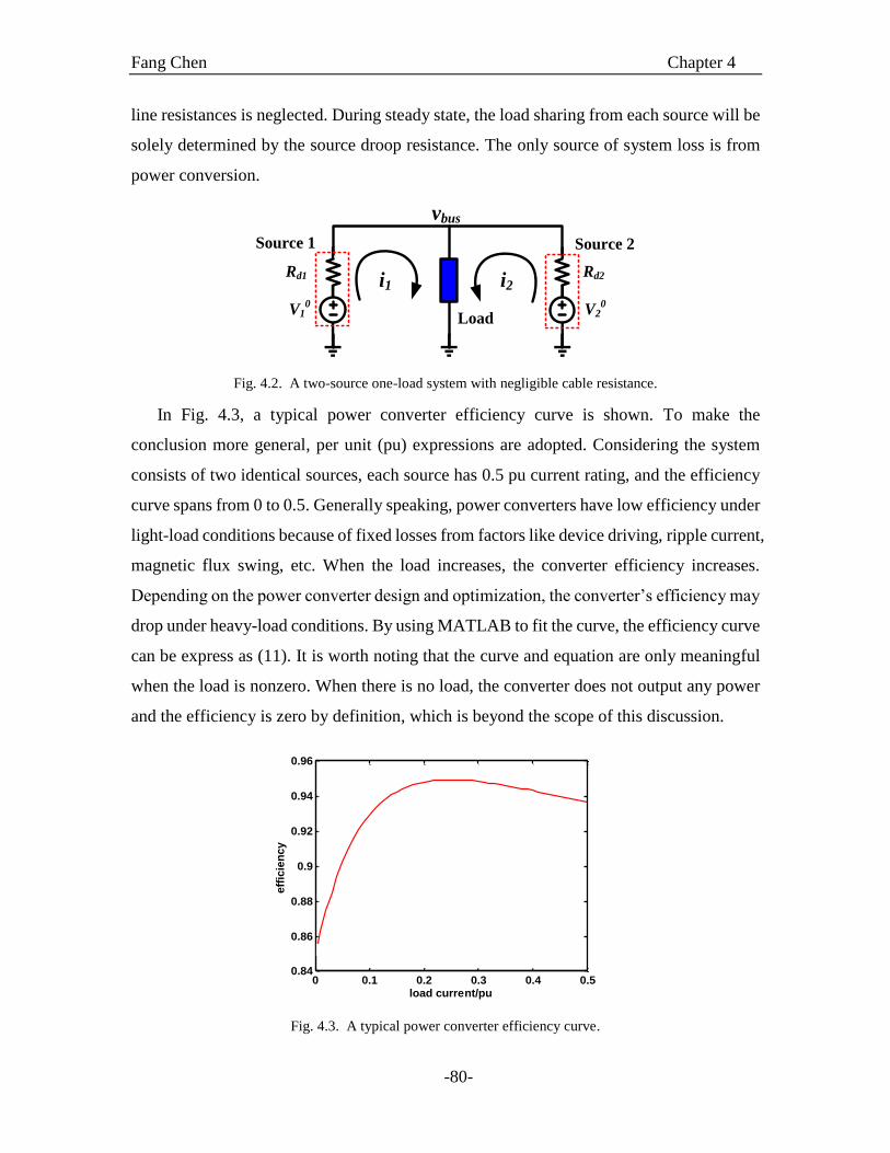
Fang Chen Chapter 4
-80-
line resistances is neglected. During steady state, the load sharing from each source will be
solely determined by the source droop resistance. The only source of system loss is from
power conversion.
LoadV1
0
i1 i2Rd1 Rd2
vbus
Source 1 Source 2
V20
Fig. 4.2. A two-source one-load system with negligible cable resistance.
In Fig. 4.3, a typical power converter efficiency curve is shown. To make the
conclusion more general, per unit (pu) expressions are adopted. Considering the system
consists of two identical sources, each source has 0.5 pu current rating, and the efficiency
curve spans from 0 to 0.5. Generally speaking, power converters have low efficiency under
light-load conditions because of fixed losses from factors like device driving, ripple current,
magnetic flux swing, etc. When the load increases, the converter efficiency increases.
Depending on the power converter design and optimization, the converter’s efficiency may
drop under heavy-load conditions. By using MATLAB to fit the curve, the efficiency curve
can be express as (11). It is worth noting that the curve and equation are only meaningful
when the load is nonzero. When there is no load, the converter does not output any power
and the efficiency is zero by definition, which is beyond the scope of this discussion.
0 0.1 0.2 0.3 0.4 0.50.84
0.86
0.88
0.9
0.92
0.94
0.96
load current/pu
eff
icie
ncy
Fig. 4.3. A typical power converter efficiency curve.

Fang Chen Chapter 4
-81-
28 10 120.975 0.1257i ii e e (11)
For a certain load current iLoad, it can be arbitrarily distributed between the two sources
by adjusting the droop parameters. If the currents from the two sources are i1 and i2, then
1 2 1 2, 0 , 0.5Loadi i i where i i (12)
The system efficiency η can then be expressed as a function of the load distribution:
1 2 1 2
1 2 1 1 2 2
1 2
1 1 2 2
1 2
1 1 2 2
/ /
/ /
/ /
o o o o
in in o o
bus bus
bus bus
P P P P
P P P P
v i v i
v i i v i i
i i
i i i i
(13)
Pin1, Pin2, Po1 and Po2 are the input and output power of the two sources, and η is the
power conversion efficiency for each source, which is a function of the output current.
Thus when the load distribution changes, the system efficiency will also change.
The higher and lower limits of the system efficiency are calculated by scanning
different load distributions, and they are illustrated with the corresponding load sharing in
Fig. 4.4 and Fig. 4.5. It can be seen that to achieve higher system efficiency, under light-
load conditions, uneven load distribution is preferred. When the load increases above a
certain threshold, even distribution is better. When the source efficiency curve changes, the
threshold also changes.
0 0.2 0.4 0.6 0.8 10.84
0.86
0.88
0.9
0.92
0.94
0.96
load current/pu
eff
icie
ncy
Higher limit
Lower limit
Fig. 4.4. Two-source paralleling efficiency.
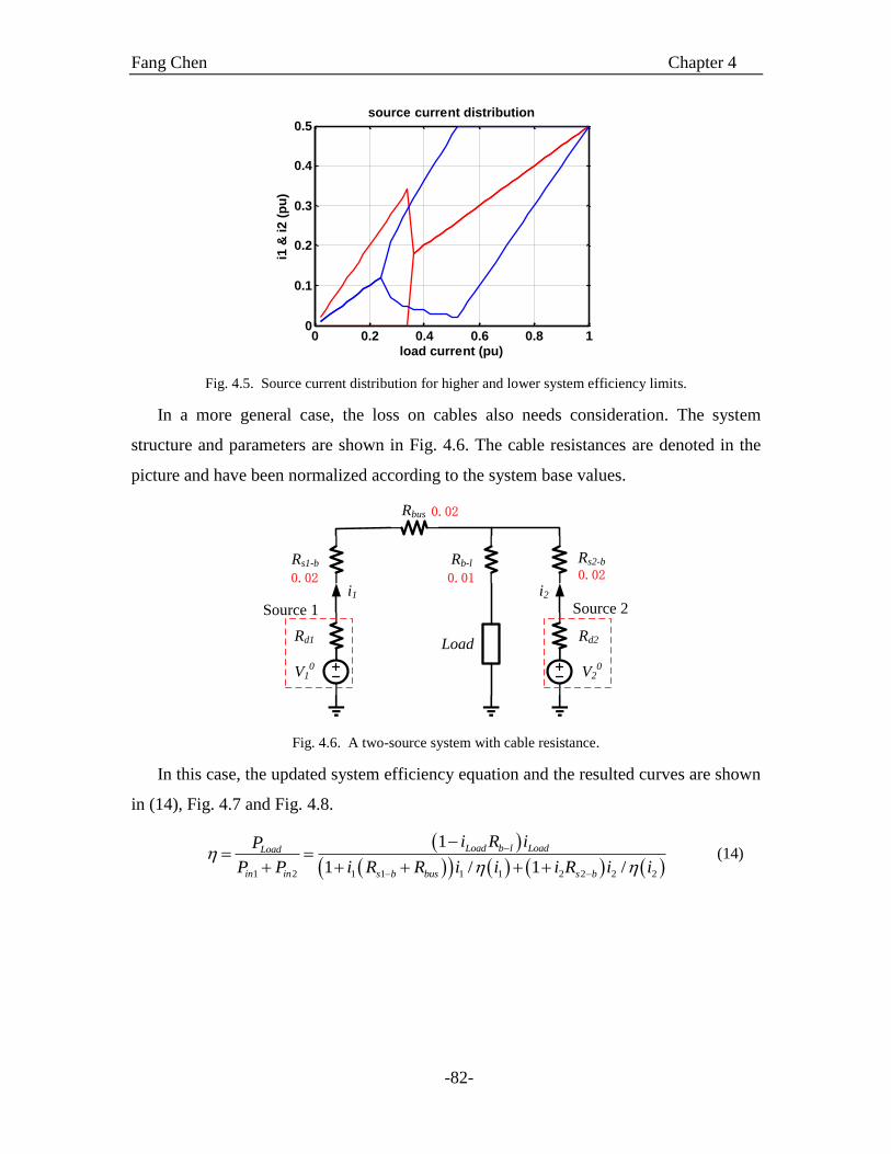
Fang Chen Chapter 4
-82-
Fig. 4.5. Source current distribution for higher and lower system efficiency limits.
In a more general case, the loss on cables also needs consideration. The system
structure and parameters are shown in Fig. 4.6. The cable resistances are denoted in the
picture and have been normalized according to the system base values.
V10
Load
i1 i2
Rd1 Rd2
Source 1 Source 2
V20
Rs1-b Rs2-b
Rbus
Rb-l
0.02
0.02
0.020.01
Fig. 4.6. A two-source system with cable resistance.
In this case, the updated system efficiency equation and the resulted curves are shown
in (14), Fig. 4.7 and Fig. 4.8.
1 2 1 1 1 1 2 2 2 2
1
1 / 1 /
Load b l LoadLoad
in in s b bus s b
i R iP
P P i R R i i i R i i
(14)
0 0.2 0.4 0.6 0.8 10
0.1
0.2
0.3
0.4
0.5
load current (pu)
i1 &
i2
(p
u)
source current distribution
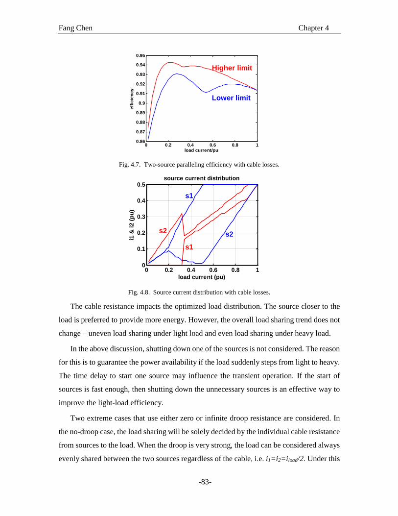
Fang Chen Chapter 4
-83-
0 0.2 0.4 0.6 0.8 10.86
0.87
0.88
0.89
0.9
0.91
0.92
0.93
0.94
0.95
load current/pu
eff
icie
ncy
Higher limit
Lower limit
Fig. 4.7. Two-source paralleling efficiency with cable losses.
0 0.2 0.4 0.6 0.8 10
0.1
0.2
0.3
0.4
0.5source current distribution
load current (pu)
i1 &
i2 (
pu
)
s2
s1
s1
s2
Fig. 4.8. Source current distribution with cable losses.
The cable resistance impacts the optimized load distribution. The source closer to the
load is preferred to provide more energy. However, the overall load sharing trend does not
change – uneven load sharing under light load and even load sharing under heavy load.
In the above discussion, shutting down one of the sources is not considered. The reason
for this is to guarantee the power availability if the load suddenly steps from light to heavy.
The time delay to start one source may influence the transient operation. If the start of
sources is fast enough, then shutting down the unnecessary sources is an effective way to
improve the light-load efficiency.
Two extreme cases that use either zero or infinite droop resistance are considered. In
the no-droop case, the load sharing will be solely decided by the individual cable resistance
from sources to the load. When the droop is very strong, the load can be considered always
evenly shared between the two sources regardless of the cable, i.e. i1=i2=iload/2. Under this
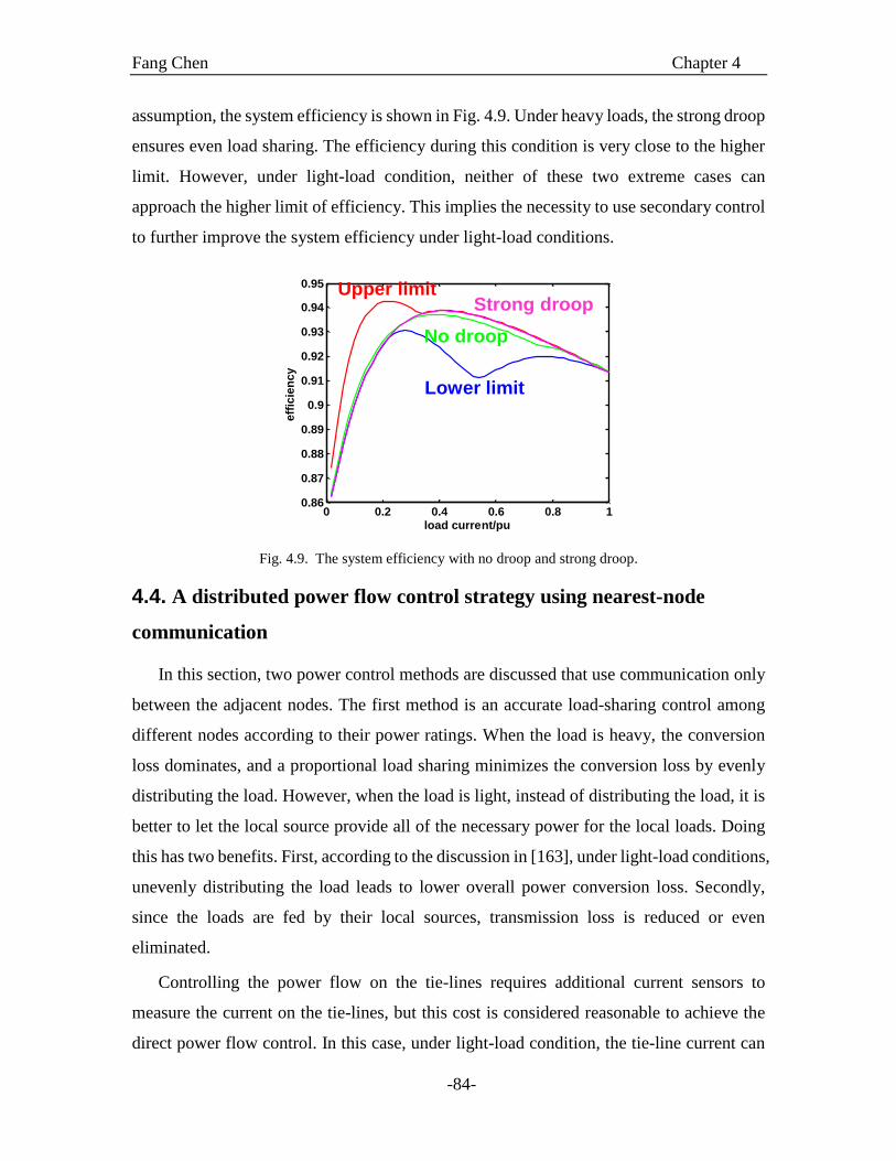
Fang Chen Chapter 4
-84-
assumption, the system efficiency is shown in Fig. 4.9. Under heavy loads, the strong droop
ensures even load sharing. The efficiency during this condition is very close to the higher
limit. However, under light-load condition, neither of these two extreme cases can
approach the higher limit of efficiency. This implies the necessity to use secondary control
to further improve the system efficiency under light-load conditions.
0 0.2 0.4 0.6 0.8 10.86
0.87
0.88
0.89
0.9
0.91
0.92
0.93
0.94
0.95
load current/pu
eff
icie
ncy
Upper limit
Lower limit
No droop
Strong droop
Fig. 4.9. The system efficiency with no droop and strong droop.
4.4. A distributed power flow control strategy using nearest-node
communication
In this section, two power control methods are discussed that use communication only
between the adjacent nodes. The first method is an accurate load-sharing control among
different nodes according to their power ratings. When the load is heavy, the conversion
loss dominates, and a proportional load sharing minimizes the conversion loss by evenly
distributing the load. However, when the load is light, instead of distributing the load, it is
better to let the local source provide all of the necessary power for the local loads. Doing
this has two benefits. First, according to the discussion in [163], under light-load conditions,
unevenly distributing the load leads to lower overall power conversion loss. Secondly,
since the loads are fed by their local sources, transmission loss is reduced or even
eliminated.
Controlling the power flow on the tie-lines requires additional current sensors to
measure the current on the tie-lines, but this cost is considered reasonable to achieve the
direct power flow control. In this case, under light-load condition, the tie-line current can

Fang Chen Chapter 4
-85-
be controlled to be zero. The transmission loss on the lines is eliminated. Under heavy-load
conditions, e.g., when the load is above 60% of the source rating, the control can switch to
the proportional sharing mode to guarantee the system availability.
Because of the droop characteristic of VRs, the steady-state bus voltage will be lower
than the nominal voltage, which may deteriorate the system performance and lower the
system efficiency due to the relatively larger current and transmission loss. Hence for both
control methods, a voltage restoration method is applied to compensate the steady-state
error. Again, this requires communication only between adjacent nodes.
The summarized system power and communication graph is shown in Fig. 4.10. The
information transmitted between adjacent nodes includes only the local voltage and current
values in pu. Each node also senses its local tie-line current for the tie-line power control.
All the measurements are localized and the communication can be low-speed. By such
means, the following three performance improvements can be achieved: (1) bus voltage
restoration; (2) load sharing enhancement; (3) tie-line current control. It is worth
mentioning that, except for the first or the last node, the communication between adjacent
nodes can be either bidirectional or unidirectional. In this chapter, to demonstrate the
simplicity of the proposed method, unidirectional communication is used. This means the
voltage and current information can be transferred from node i-1 to node i, and then to node
i+1, but not in the reverse direction.
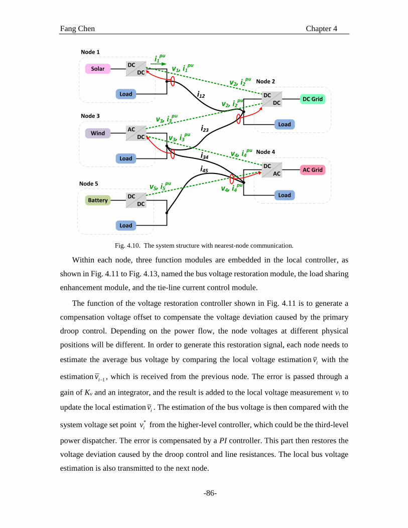
Fang Chen Chapter 4
-86-
Node 4
Node 5
Node 3
DCDC
Solar
Load
ACDC
Wind
Load
DCDC
Battery
Load
DCDC
DC Grid
Load
DCAC
AC Grid
Load
Node 1
Node 2
v1, i1pu
v4, i4puv5, i5
pu
i12
i23
i34
i45
i1pu
v2, i2pu
v3, i3pu
v4, i4pu
v2, i2pu
v3, i3pu
Fig. 4.10. The system structure with nearest-node communication.
Within each node, three function modules are embedded in the local controller, as
shown in Fig. 4.11 to Fig. 4.13, named the bus voltage restoration module, the load sharing
enhancement module, and the tie-line current control module.
The function of the voltage restoration controller shown in Fig. 4.11 is to generate a
compensation voltage offset to compensate the voltage deviation caused by the primary
droop control. Depending on the power flow, the node voltages at different physical
positions will be different. In order to generate this restoration signal, each node needs to
estimate the average bus voltage by comparing the local voltage estimationiv with the
estimation1iv , which is received from the previous node. The error is passed through a
gain of Kv and an integrator, and the result is added to the local voltage measurement vi to
update the local estimation iv . The estimation of the bus voltage is then compared with the
system voltage set point *
iv from the higher-level controller, which could be the third-level
power dispatcher. The error is compensated by a PI controller. This part then restores the
voltage deviation caused by the droop control and line resistances. The local bus voltage
estimation is also transmitted to the next node.
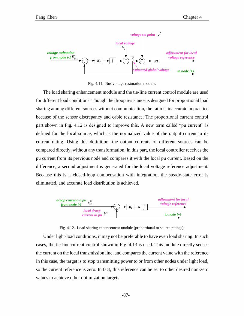
Fang Chen Chapter 4
-87-
voltage estimation
from node i-1iv
Kv
1iv
iv
-+ ++
*
iv
+- PI
voltage set point
local voltage
estimated global voltage to node i+1
adjustment for local
voltage reference
Fig. 4.11. Bus voltage restoration module.
The load sharing enhancement module and the tie-line current control module are used
for different load conditions. Though the droop resistance is designed for proportional load
sharing among different sources without communication, the ratio is inaccurate in practice
because of the sensor discrepancy and cable resistance. The proportional current control
part shown in Fig. 4.12 is designed to improve this. A new term called “pu current” is
defined for the local source, which is the normalized value of the output current to its
current rating. Using this definition, the output currents of different sources can be
compared directly, without any transformation. In this part, the local controller receives the
pu current from its previous node and compares it with the local pu current. Based on the
difference, a second adjustment is generated for the local voltage reference adjustment.
Because this is a closed-loop compensation with integration, the steady-state error is
eliminated, and accurate load distribution is achieved.
Ki
1
pu
ii
pu
ii
droop current in pu
from node i-1
local droop
current in pu
adjustment for local
voltage reference
to node i+1
-+
Fig. 4.12. Load sharing enhancement module (proportional to source ratings).
Under light-load conditions, it may not be preferable to have even load sharing. In such
cases, the tie-line current control shown in Fig. 4.13 is used. This module directly senses
the current on the local transmission line, and compares the current value with the reference.
In this case, the target is to stop transmitting power to or from other nodes under light load,
so the current reference is zero. In fact, this reference can be set to other desired non-zero
values to achieve other optimization targets.
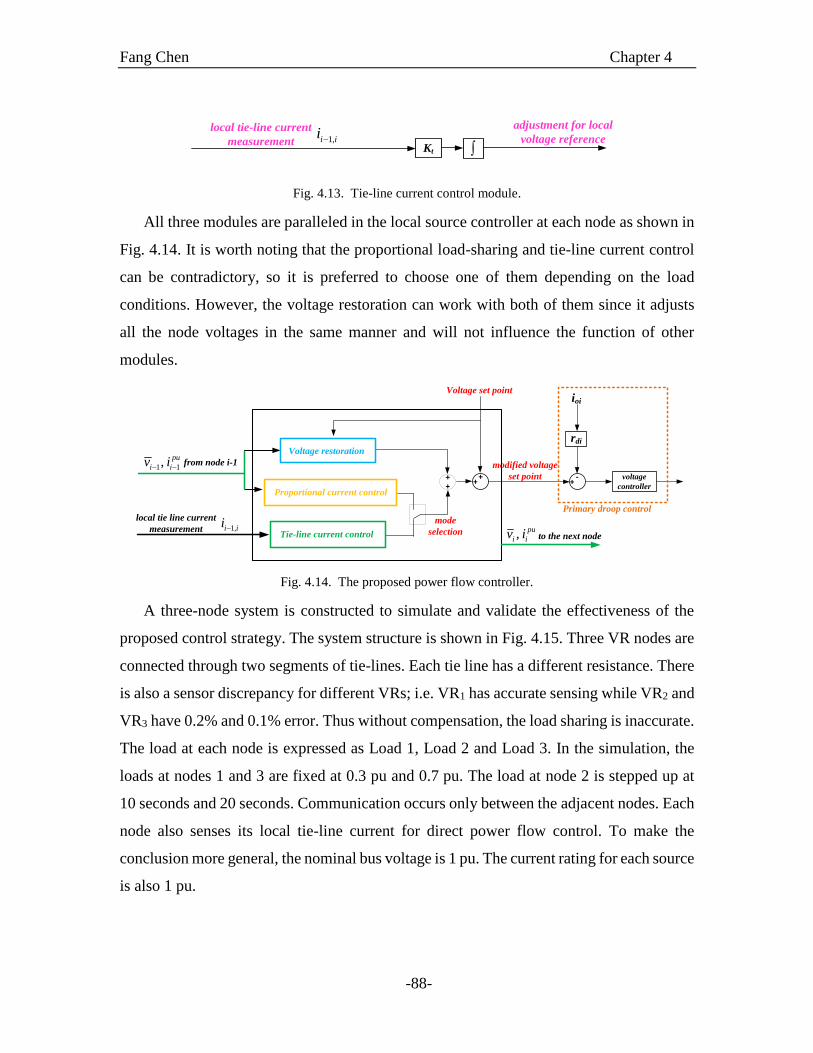
Fang Chen Chapter 4
-88-
Kt
local tie-line current
measurement
adjustment for local
voltage reference1,i ii
Fig. 4.13. Tie-line current control module.
All three modules are paralleled in the local source controller at each node as shown in
Fig. 4.14. It is worth noting that the proportional load-sharing and tie-line current control
can be contradictory, so it is preferred to choose one of them depending on the load
conditions. However, the voltage restoration can work with both of them since it adjusts
all the node voltages in the same manner and will not influence the function of other
modules.
++ +
+
modified voltage
set point -+
rdi
ioi
voltage
controller
Primary droop control
Voltage restoration
Proportional current control
Tie-line current control
Voltage set point
from node i-1
local tie line current
measurementto the next node
mode
selection
1 1, pu
i iv i
1,i ii , pu
i iv i
Fig. 4.14. The proposed power flow controller.
A three-node system is constructed to simulate and validate the effectiveness of the
proposed control strategy. The system structure is shown in Fig. 4.15. Three VR nodes are
connected through two segments of tie-lines. Each tie line has a different resistance. There
is also a sensor discrepancy for different VRs; i.e. VR1 has accurate sensing while VR2 and
VR3 have 0.2% and 0.1% error. Thus without compensation, the load sharing is inaccurate.
The load at each node is expressed as Load 1, Load 2 and Load 3. In the simulation, the
loads at nodes 1 and 3 are fixed at 0.3 pu and 0.7 pu. The load at node 2 is stepped up at
10 seconds and 20 seconds. Communication occurs only between the adjacent nodes. Each
node also senses its local tie-line current for direct power flow control. To make the
conclusion more general, the nominal bus voltage is 1 pu. The current rating for each source
is also 1 pu.
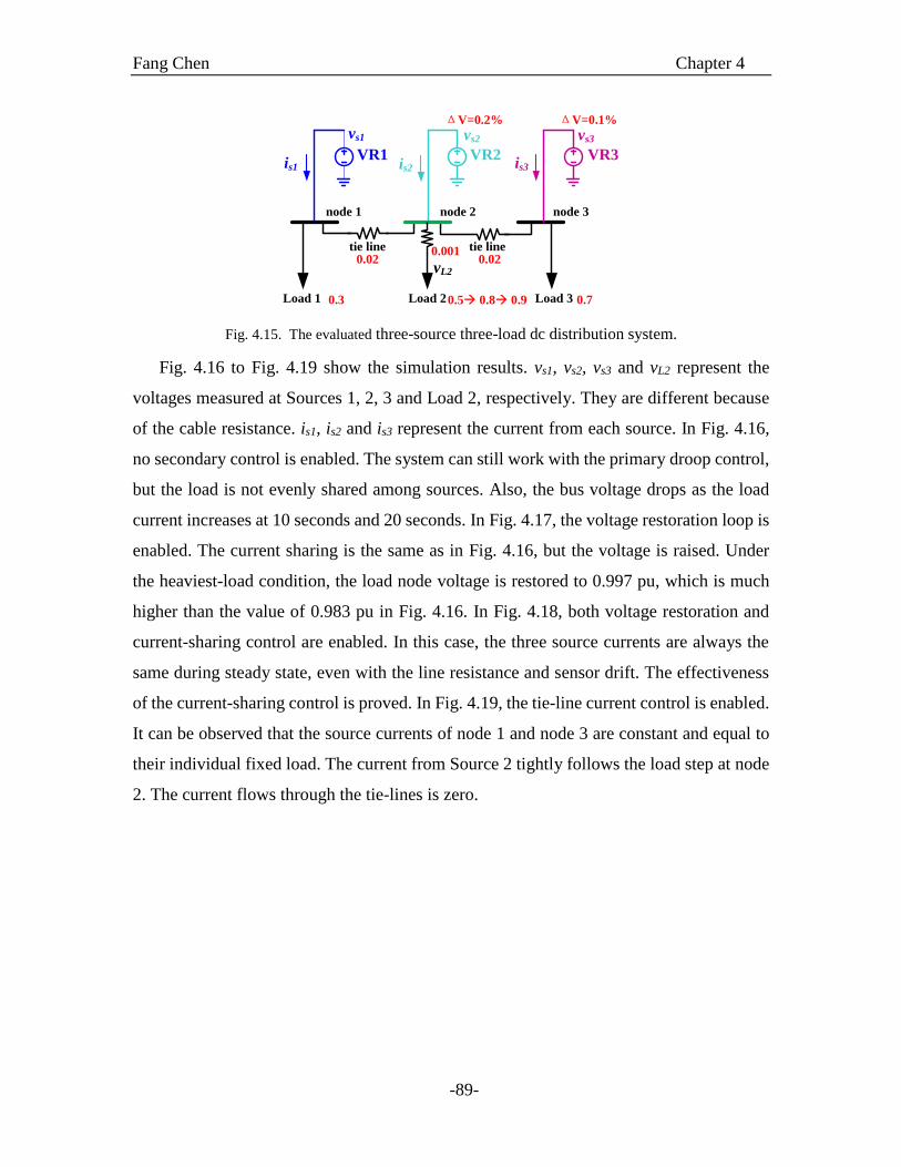
Fang Chen Chapter 4
-89-
node 1 node 2 node 3
tie line tie line
Load 1 Load 2 Load 3
is1 is2 is3VR1 VR2 VR3
0.02 0.02
0.3 0.70.5à 0.8à 0.9
ΔV=0.2% ΔV=0.1%
0.001
vs1 vs2 vs3
vL2
Fig. 4.15. The evaluated three-source three-load dc distribution system.
Fig. 4.16 to Fig. 4.19 show the simulation results. vs1, vs2, vs3 and vL2 represent the
voltages measured at Sources 1, 2, 3 and Load 2, respectively. They are different because
of the cable resistance. is1, is2 and is3 represent the current from each source. In Fig. 4.16,
no secondary control is enabled. The system can still work with the primary droop control,
but the load is not evenly shared among sources. Also, the bus voltage drops as the load
current increases at 10 seconds and 20 seconds. In Fig. 4.17, the voltage restoration loop is
enabled. The current sharing is the same as in Fig. 4.16, but the voltage is raised. Under
the heaviest-load condition, the load node voltage is restored to 0.997 pu, which is much
higher than the value of 0.983 pu in Fig. 4.16. In Fig. 4.18, both voltage restoration and
current-sharing control are enabled. In this case, the three source currents are always the
same during steady state, even with the line resistance and sensor drift. The effectiveness
of the current-sharing control is proved. In Fig. 4.19, the tie-line current control is enabled.
It can be observed that the source currents of node 1 and node 3 are constant and equal to
their individual fixed load. The current from Source 2 tightly follows the load step at node
2. The current flows through the tie-lines is zero.
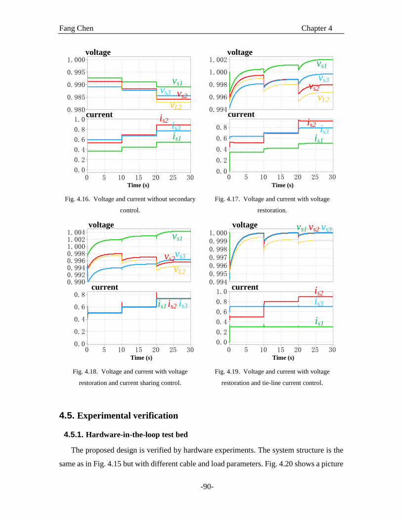
Fang Chen Chapter 4
-90-
vs1
vs2vs3
vL2
Time (s)
voltage
current
is1
is3
is2
Fig. 4.16. Voltage and current without secondary
control.
voltage
current
Time (s)
is1
is3
is2
vs1
vs3vs2
vL2
Fig. 4.17. Voltage and current with voltage
restoration.
Time (s)
voltage
current
vs1
vs2vs3
vL2
is1 is3is2
Fig. 4.18. Voltage and current with voltage
restoration and current sharing control.
Time (s)
voltage
current
vs1 vs2 vs3
is2
is3
is1
Fig. 4.19. Voltage and current with voltage
restoration and tie-line current control.
4.5. Experimental verification
4.5.1. Hardware-in-the-loop test bed
The proposed design is verified by hardware experiments. The system structure is the
same as in Fig. 4.15 but with different cable and load parameters. Fig. 4.20 shows a picture
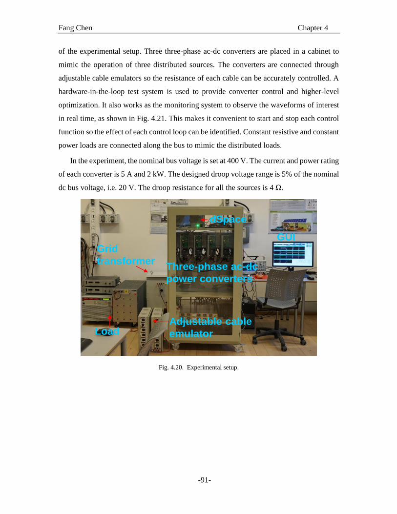
Fang Chen Chapter 4
-91-
of the experimental setup. Three three-phase ac-dc converters are placed in a cabinet to
mimic the operation of three distributed sources. The converters are connected through
adjustable cable emulators so the resistance of each cable can be accurately controlled. A
hardware-in-the-loop test system is used to provide converter control and higher-level
optimization. It also works as the monitoring system to observe the waveforms of interest
in real time, as shown in Fig. 4.21. This makes it convenient to start and stop each control
function so the effect of each control loop can be identified. Constant resistive and constant
power loads are connected along the bus to mimic the distributed loads.
In the experiment, the nominal bus voltage is set at 400 V. The current and power rating
of each converter is 5 A and 2 kW. The designed droop voltage range is 5% of the nominal
dc bus voltage, i.e. 20 V. The droop resistance for all the sources is 4 Ω.
dSpace
LoadAdjustable cable
emulator
GUIGrid
transformerThree-phase ac-dc
power converters
Fig. 4.20. Experimental setup.
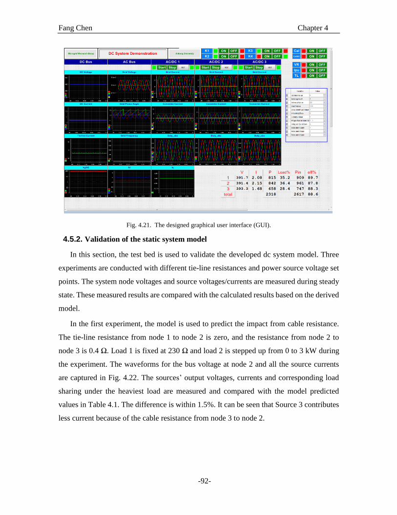
Fang Chen Chapter 4
-92-
Fig. 4.21. The designed graphical user interface (GUI).
4.5.2. Validation of the static system model
In this section, the test bed is used to validate the developed dc system model. Three
experiments are conducted with different tie-line resistances and power source voltage set
points. The system node voltages and source voltages/currents are measured during steady
state. These measured results are compared with the calculated results based on the derived
model.
In the first experiment, the model is used to predict the impact from cable resistance.
The tie-line resistance from node 1 to node 2 is zero, and the resistance from node 2 to
node 3 is 0.4 Ω. Load 1 is fixed at 230 Ω and load 2 is stepped up from 0 to 3 kW during
the experiment. The waveforms for the bus voltage at node 2 and all the source currents
are captured in Fig. 4.22. The sources’ output voltages, currents and corresponding load
sharing under the heaviest load are measured and compared with the model predicted
values in Table 4.1. The difference is within 1.5%. It can be seen that Source 3 contributes
less current because of the cable resistance from node 3 to node 2.
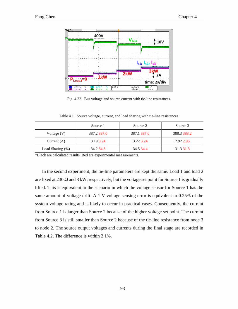
Fang Chen Chapter 4
-93-
Vbus
Is1, Is2, Is3
400V
time: 2s/div
2A
10V
PLoad2=01kW
2kW3kW
Fig. 4.22. Bus voltage and source current with tie-line resistances.
Table 4.1. Source voltage, current, and load sharing with tie-line resistances.
Source 1 Source 2 Source 3
Voltage (V) 387.2 387.0 387.1 387.0 388.3 388.2
Current (A) 3.19 3.24 3.22 3.24 2.92 2.95
Load Sharing (%) 34.2 34.3 34.5 34.4 31.3 31.3
*Black are calculated results. Red are experimental measurements.
In the second experiment, the tie-line parameters are kept the same. Load 1 and load 2
are fixed at 230 Ω and 3 kW, respectively, but the voltage set point for Source 1 is gradually
lifted. This is equivalent to the scenario in which the voltage sensor for Source 1 has the
same amount of voltage drift. A 1 V voltage sensing error is equivalent to 0.25% of the
system voltage rating and is likely to occur in practical cases. Consequently, the current
from Source 1 is larger than Source 2 because of the higher voltage set point. The current
from Source 3 is still smaller than Source 2 because of the tie-line resistance from node 3
to node 2. The source output voltages and currents during the final stage are recorded in
Table 4.2. The difference is within 2.1%.
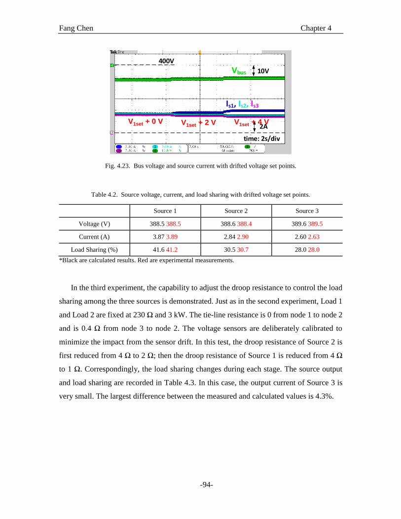
Fang Chen Chapter 4
-94-
Vbus
Is1, Is2, Is3
400V
time: 2s/div
2A
10V
V1set + 0 V V1set + 2 V V1set + 4 V
Fig. 4.23. Bus voltage and source current with drifted voltage set points.
Table 4.2. Source voltage, current, and load sharing with drifted voltage set points.
Source 1 Source 2 Source 3
Voltage (V) 388.5 388.5 388.6 388.4 389.6 389.5
Current (A) 3.87 3.89 2.84 2.90 2.60 2.63
Load Sharing (%) 41.6 41.2 30.5 30.7 28.0 28.0
*Black are calculated results. Red are experimental measurements.
In the third experiment, the capability to adjust the droop resistance to control the load
sharing among the three sources is demonstrated. Just as in the second experiment, Load 1
and Load 2 are fixed at 230 Ω and 3 kW. The tie-line resistance is 0 from node 1 to node 2
and is 0.4 Ω from node 3 to node 2. The voltage sensors are deliberately calibrated to
minimize the impact from the sensor drift. In this test, the droop resistance of Source 2 is
first reduced from 4 Ω to 2 Ω; then the droop resistance of Source 1 is reduced from 4 Ω
to 1 Ω. Correspondingly, the load sharing changes during each stage. The source output
and load sharing are recorded in Table 4.3. In this case, the output current of Source 3 is
very small. The largest difference between the measured and calculated values is 4.3%.
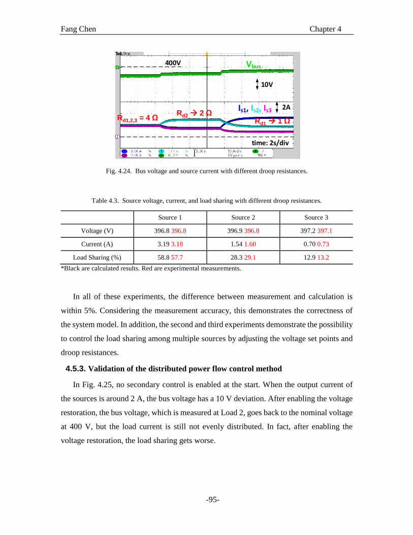
Fang Chen Chapter 4
-95-
Vbus
Is1, Is2, Is3
400V
time: 2s/div
10V
2A
Rd1 à 1 ΩRd2 à 2 Ω
Rd1,2,3 = 4 Ω
Fig. 4.24. Bus voltage and source current with different droop resistances.
Table 4.3. Source voltage, current, and load sharing with different droop resistances.
Source 1 Source 2 Source 3
Voltage (V) 396.8 396.8 396.9 396.8 397.2 397.1
Current (A) 3.19 3.18 1.54 1.60 0.70 0.73
Load Sharing (%) 58.8 57.7 28.3 29.1 12.9 13.2
*Black are calculated results. Red are experimental measurements.
In all of these experiments, the difference between measurement and calculation is
within 5%. Considering the measurement accuracy, this demonstrates the correctness of
the system model. In addition, the second and third experiments demonstrate the possibility
to control the load sharing among multiple sources by adjusting the voltage set points and
droop resistances.
4.5.3. Validation of the distributed power flow control method
In Fig. 4.25, no secondary control is enabled at the start. When the output current of
the sources is around 2 A, the bus voltage has a 10 V deviation. After enabling the voltage
restoration, the bus voltage, which is measured at Load 2, goes back to the nominal voltage
at 400 V, but the load current is still not evenly distributed. In fact, after enabling the
voltage restoration, the load sharing gets worse.
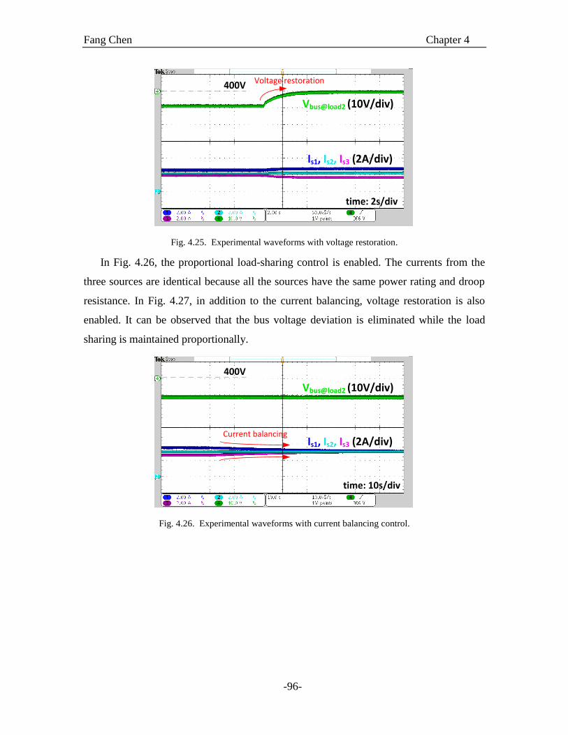
Fang Chen Chapter 4
-96-
Vbus@load2 (10V/div)
Is1, Is2, Is3 (2A/div)
400V
time: 2s/div
Voltage restoration
Fig. 4.25. Experimental waveforms with voltage restoration.
In Fig. 4.26, the proportional load-sharing control is enabled. The currents from the
three sources are identical because all the sources have the same power rating and droop
resistance. In Fig. 4.27, in addition to the current balancing, voltage restoration is also
enabled. It can be observed that the bus voltage deviation is eliminated while the load
sharing is maintained proportionally.
Vbus@load2 (10V/div)
Is1, Is2, Is3 (2A/div)
400V
time: 10s/div
Current balancing
Fig. 4.26. Experimental waveforms with current balancing control.
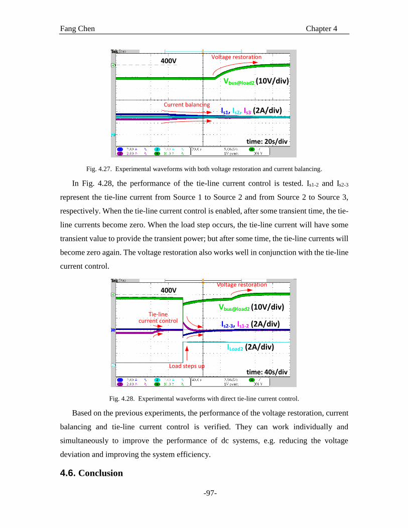
Fang Chen Chapter 4
-97-
Vbus@load2 (10V/div)
Is1, Is2, Is3 (2A/div)
400V
time: 20s/div
Current balancing
Voltage restoration
Fig. 4.27. Experimental waveforms with both voltage restoration and current balancing.
In Fig. 4.28, the performance of the tie-line current control is tested. Is1-2 and Is2-3
represent the tie-line current from Source 1 to Source 2 and from Source 2 to Source 3,
respectively. When the tie-line current control is enabled, after some transient time, the tie-
line currents become zero. When the load step occurs, the tie-line current will have some
transient value to provide the transient power; but after some time, the tie-line currents will
become zero again. The voltage restoration also works well in conjunction with the tie-line
current control.
Vbus@load2 (10V/div)
Is2-3, Is1-2 (2A/div)
400V
time: 40s/div
ILoad2 (2A/div)
Tie-line current control
Load steps up
Voltage restoration
Fig. 4.28. Experimental waveforms with direct tie-line current control.
Based on the previous experiments, the performance of the voltage restoration, current
balancing and tie-line current control is verified. They can work individually and
simultaneously to improve the performance of dc systems, e.g. reducing the voltage
deviation and improving the system efficiency.
4.6. Conclusion

Fang Chen Chapter 4
-98-
In this chapter, the analytical solution for power flow in a generic dc system is derived.
Based on it, the power flow optimization can be realized. This chapter focuses on the
secondary control to improve system efficiency, which prefers even load sharing under
heavy-load conditions and uneven load sharing under light-load conditions. A voltage
restoration method based on nearest-node communication is used to restore the voltage
deviation caused by the droop characteristic. A proportional current regulator is adopted to
accurately control the load sharing with realistic sensor drifts and line resistances. A tie-
line power flow control method is proposed to regulate the tie-line current and reduce the
power transmission loss. All of the considered methods need only the local measurements
and information from its nearest node; thus system expandability is guaranteed.

Fang Chen Chapter 5
-99-
Chapter 5. A HIGH-EFFICIENCY TRANSFORMER-LESS SINGLE-
PHASE UTILITY-INTERFACE CONVERTER FOR 380 V DC
MICROGRIDS
In this chapter, a high-efficiency two-stage single-phase ac-dc converter is designed to
connect a 380 V bipolar dc microgrid with a 240 V split-phase single-phase ac system. The
design requirements on the ac and dc interfaces are summarized. The efficiency of the
converters using different phase-leg structures is evaluated, based on which a two-level
interleaved topology using state-of-the-art Silicon Carbide (SiC) MOSFETs is chosen. A
pluggable phase-leg module with embedded driving and protection circuit is designed and
tested. Interleaving angles are selected to achieve an optimized magnetics design. A 10 kW
converter prototype is built and achieves an efficiency higher than 97%.
Besides the high efficiency, a common-mode (CM) equivalent circuit is established for
the converter systems. A CM voltage controller is designed for the dc-dc stage to control
the dc bus CM voltages. The resultant dc bus voltages are symmetric to the ground and
suitable for bipolar dc power distribution systems.
5.1. Design application and requirements
5.1.1. Gird-interface converter for future residential houses
To connect renewable sources and energy storage, dc power distribution has arisen as
an attractive solution because of the higher efficiency and reliability when compared with
ac distribution [3], [46], [167]–[170]. DC grids can be connected to the ac utility through
interface converters and exchange only the extra or insufficient energy [104], [105], [123].
Fig. 5.1 shows the schematic of a possible future residential dc power distribution system.
Renewables, energy storage, and different kinds of loads are connected to a common 380 V
dc bus through power converters. Then the dc system is interfaced to the ac utility through
a bidirectional ac-dc interface converter. This converter provides bidirectional power flow,
regulates the ac current and dc voltage, and decouples the dynamics of both systems. To
cover the power consumption of a normal U.S. family, the target converter power rating is
10 kVA.
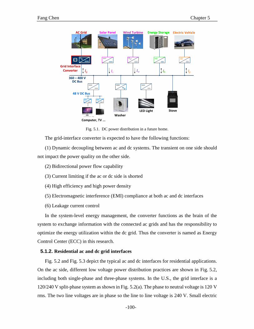
Fang Chen Chapter 5
-100-
AC Grid
μC
Grid Interface Converter Ig Is Ib
360 – 400 V DC Bus
Iw
Solar Panel Wind Turbine Energy Storage Electric Vehicle
Ip
Washer
Stove
48 V DC Bus
Computer, TV ...
μCLED Light
M
μC
Fig. 5.1. DC power distribution in a future home.
The grid-interface converter is expected to have the following functions:
(1) Dynamic decoupling between ac and dc systems. The transient on one side should
not impact the power quality on the other side.
(2) Bidirectional power flow capability
(3) Current limiting if the ac or dc side is shorted
(4) High efficiency and high power density
(5) Electromagnetic interference (EMI) compliance at both ac and dc interfaces
(6) Leakage current control
In the system-level energy management, the converter functions as the brain of the
system to exchange information with the connected ac grids and has the responsibility to
optimize the energy utilization within the dc grid. Thus the converter is named as Energy
Control Center (ECC) in this research.
5.1.2. Residential ac and dc grid interfaces
Fig. 5.2 and Fig. 5.3 depict the typical ac and dc interfaces for residential applications.
On the ac side, different low voltage power distribution practices are shown in Fig. 5.2,
including both single-phase and three-phase systems. In the U.S., the grid interface is a
120/240 V split-phase system as shown in Fig. 5.2(a). The phase to neutral voltage is 120 V
rms. The two line voltages are in phase so the line to line voltage is 240 V. Small electric
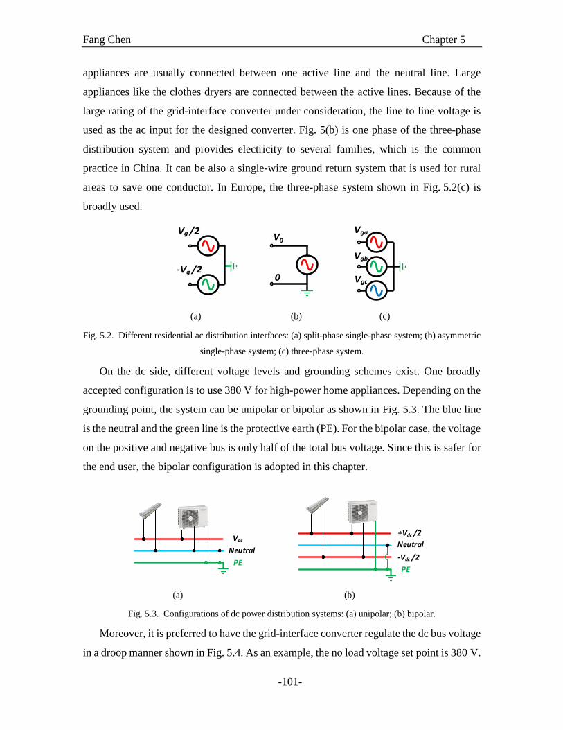
Fang Chen Chapter 5
-101-
appliances are usually connected between one active line and the neutral line. Large
appliances like the clothes dryers are connected between the active lines. Because of the
large rating of the grid-interface converter under consideration, the line to line voltage is
used as the ac input for the designed converter. Fig. 5(b) is one phase of the three-phase
distribution system and provides electricity to several families, which is the common
practice in China. It can be also a single-wire ground return system that is used for rural
areas to save one conductor. In Europe, the three-phase system shown in Fig. 5.2(c) is
broadly used.
Vg /2Vg
Vga
Vgb
Vgc
-Vg /20
(a) (b) (c)
Fig. 5.2. Different residential ac distribution interfaces: (a) split-phase single-phase system; (b) asymmetric
single-phase system; (c) three-phase system.
On the dc side, different voltage levels and grounding schemes exist. One broadly
accepted configuration is to use 380 V for high-power home appliances. Depending on the
grounding point, the system can be unipolar or bipolar as shown in Fig. 5.3. The blue line
is the neutral and the green line is the protective earth (PE). For the bipolar case, the voltage
on the positive and negative bus is only half of the total bus voltage. Since this is safer for
the end user, the bipolar configuration is adopted in this chapter.
+Vdc /2
-Vdc /2
PE
Vdc
PE
NeutralNeutral
(a) (b)
Fig. 5.3. Configurations of dc power distribution systems: (a) unipolar; (b) bipolar.
Moreover, it is preferred to have the grid-interface converter regulate the dc bus voltage
in a droop manner shown in Fig. 5.4. As an example, the no load voltage set point is 380 V.
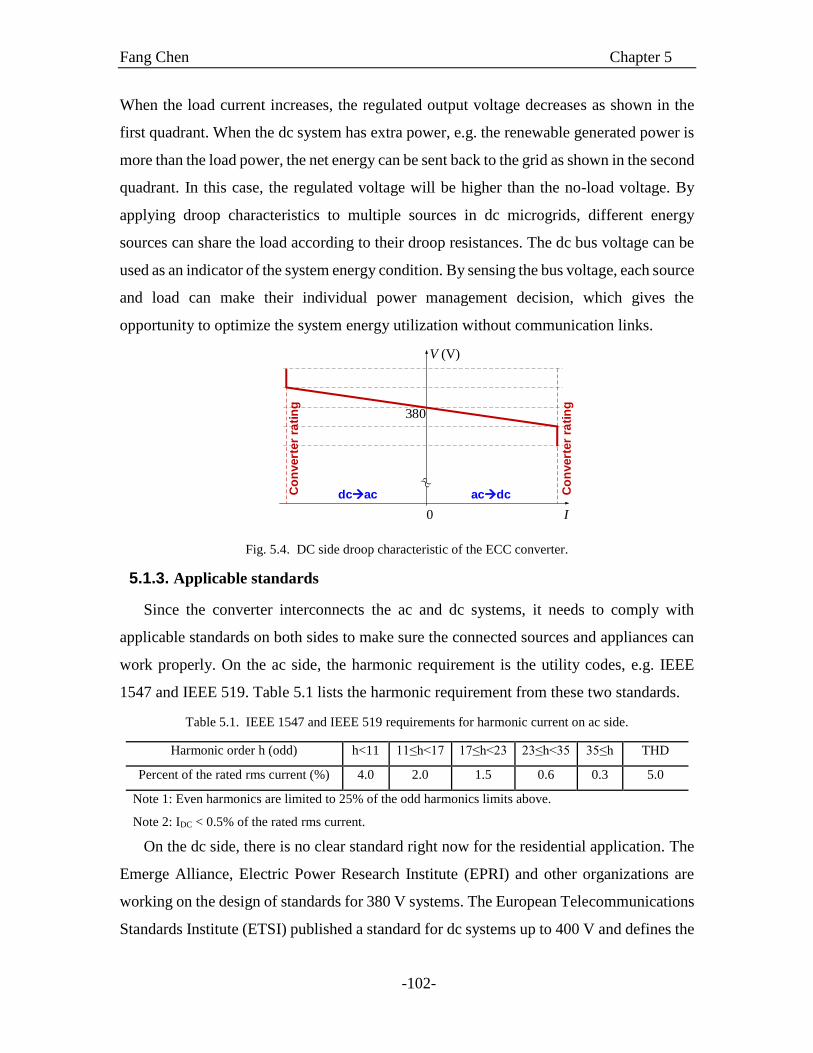
Fang Chen Chapter 5
-102-
When the load current increases, the regulated output voltage decreases as shown in the
first quadrant. When the dc system has extra power, e.g. the renewable generated power is
more than the load power, the net energy can be sent back to the grid as shown in the second
quadrant. In this case, the regulated voltage will be higher than the no-load voltage. By
applying droop characteristics to multiple sources in dc microgrids, different energy
sources can share the load according to their droop resistances. The dc bus voltage can be
used as an indicator of the system energy condition. By sensing the bus voltage, each source
and load can make their individual power management decision, which gives the
opportunity to optimize the system energy utilization without communication links.
Co
nvert
er
rati
ng
Co
nvert
er
rati
ng
V (V)
0 I
380
acàdcdcàac
Fig. 5.4. DC side droop characteristic of the ECC converter.
5.1.3. Applicable standards
Since the converter interconnects the ac and dc systems, it needs to comply with
applicable standards on both sides to make sure the connected sources and appliances can
work properly. On the ac side, the harmonic requirement is the utility codes, e.g. IEEE
1547 and IEEE 519. Table 5.1 lists the harmonic requirement from these two standards.
Table 5.1. IEEE 1547 and IEEE 519 requirements for harmonic current on ac side.
Harmonic order h (odd) h<11 11≤h<17 17≤h<23 23≤h<35 35≤h THD
Percent of the rated rms current (%) 4.0 2.0 1.5 0.6 0.3 5.0
Note 1: Even harmonics are limited to 25% of the odd harmonics limits above.
Note 2: IDC < 0.5% of the rated rms current.
On the dc side, there is no clear standard right now for the residential application. The
Emerge Alliance, Electric Power Research Institute (EPRI) and other organizations are
working on the design of standards for 380 V systems. The European Telecommunications
Standards Institute (ETSI) published a standard for dc systems up to 400 V and defines the
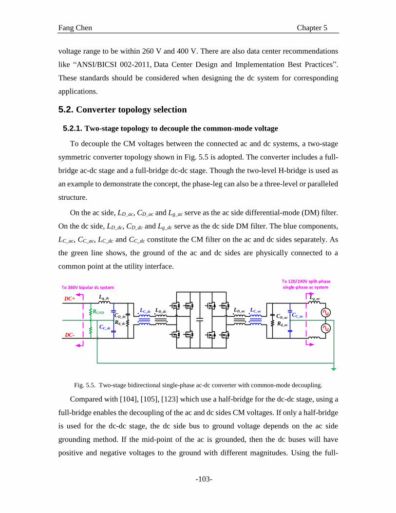
Fang Chen Chapter 5
-103-
voltage range to be within 260 V and 400 V. There are also data center recommendations
like “ANSI/BICSI 002-2011, Data Center Design and Implementation Best Practices”.
These standards should be considered when designing the dc system for corresponding
applications.
5.2. Converter topology selection
5.2.1. Two-stage topology to decouple the common-mode voltage
To decouple the CM voltages between the connected ac and dc systems, a two-stage
symmetric converter topology shown in Fig. 5.5 is adopted. The converter includes a full-
bridge ac-dc stage and a full-bridge dc-dc stage. Though the two-level H-bridge is used as
an example to demonstrate the concept, the phase-leg can also be a three-level or paralleled
structure.
On the ac side, LD_ac, CD_ac and Lg_ac serve as the ac side differential-mode (DM) filter.
On the dc side, LD_dc, CD_dc and Lg_dc serve as the dc side DM filter. The blue components,
LC_ac, CC_ac, LC_dc and CC_dc constitute the CM filter on the ac and dc sides separately. As
the green line shows, the ground of the ac and dc sides are physically connected to a
common point at the utility interface.
LD_ac LC_ac
To 120/240V split-phase single-phase ac system
CC_acCD_ac
Rd_ac
Lg_ac
LD_dcLC_dc
DC+
DC-
To 380V bipolar dc system
CD_dc
Rd_dcCC_dc
RGND
Lg_dc
Fig. 5.5. Two-stage bidirectional single-phase ac-dc converter with common-mode decoupling.
Compared with [104], [105], [123] which use a half-bridge for the dc-dc stage, using a
full-bridge enables the decoupling of the ac and dc sides CM voltages. If only a half-bridge
is used for the dc-dc stage, the dc side bus to ground voltage depends on the ac side
grounding method. If the mid-point of the ac is grounded, then the dc buses will have
positive and negative voltages to the ground with different magnitudes. Using the full-

Fang Chen Chapter 5
-104-
bridge, both the positive and negative dc bus voltages are modulated and can be any value
between the positive and negative dc-link voltages. Thus the converter has more flexibility
in controlling the dc bus to ground CM voltages.
5.2.2. Selection of the phase-leg structure to achieve high efficiency
An important requirement for the interface converter is high efficiency. The interface
converter functions as an energy router to balance the power between the ac and dc grids.
The router itself should be very efficient, especially under light load since that is where the
converter operates most of the time. To achieve a high-efficiency power stage design, the
converter efficiency is evaluated by using different phase-leg structures and state-of-the-
art semiconductor devices.
5.2.2.1. Phase-leg structure and modulation method
As shown in Fig. 5.5, the converter features a symmetric structure. In practice, the
front-end ac-dc stage contributes more loss because the ac side has a lower rms voltage and
a higher rms current than the dc side. Most of the effort in this part is to optimize the ac-dc
stage. However, the same procedure can be applied to the dc-dc stage. In fact, if the ac-dc
stage is designed to achieve a very high efficiency, the dc-dc stage that adopts the same
design will also have a high efficiency.
The simplest and broadly used topology to fulfill the bidirectional ac-dc conversion is
the two-level (2L) full-bridge topology shown in Fig. 5.6(a). The modulation method can
be unipolar, bipolar or discontinuous. The details and harmonic analysis for these
modulation methods can be found in [171]. Compared with bipolar modulation, unipolar
modulation has current harmonics at twice the switching frequency, which allows the use
of a smaller inductance to maintain the same inductor current ripple, and is used in this
comparison. To reduce the conduction loss of state-of-the-art SiC MOSFETs, a 2L full-
bridge phase-leg with paralleled devices shown in Fig. 5.6(b) is also considered. The two-
phase interleaved topology is considered to have similar efficiency to the paralleled
topology if the converter loss is mainly from the switching devices.
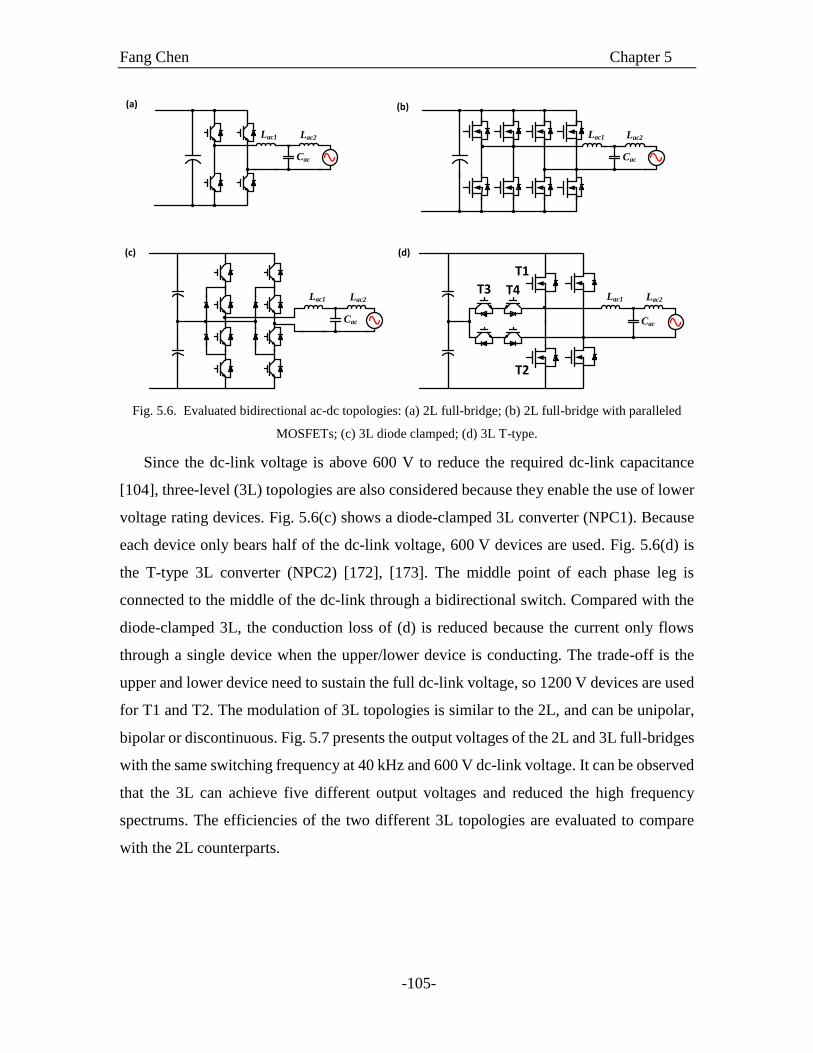
Fang Chen Chapter 5
-105-
Lac1 Lac2
Cac
(a) (b)
Lac1 Lac2
Cac
(c) (d)
Lac1 Lac2
Cac
Lac1 Lac2
Cac
T1
T2
T3 T4
Fig. 5.6. Evaluated bidirectional ac-dc topologies: (a) 2L full-bridge; (b) 2L full-bridge with paralleled
MOSFETs; (c) 3L diode clamped; (d) 3L T-type.
Since the dc-link voltage is above 600 V to reduce the required dc-link capacitance
[104], three-level (3L) topologies are also considered because they enable the use of lower
voltage rating devices. Fig. 5.6(c) shows a diode-clamped 3L converter (NPC1). Because
each device only bears half of the dc-link voltage, 600 V devices are used. Fig. 5.6(d) is
the T-type 3L converter (NPC2) [172], [173]. The middle point of each phase leg is
connected to the middle of the dc-link through a bidirectional switch. Compared with the
diode-clamped 3L, the conduction loss of (d) is reduced because the current only flows
through a single device when the upper/lower device is conducting. The trade-off is the
upper and lower device need to sustain the full dc-link voltage, so 1200 V devices are used
for T1 and T2. The modulation of 3L topologies is similar to the 2L, and can be unipolar,
bipolar or discontinuous. Fig. 5.7 presents the output voltages of the 2L and 3L full-bridges
with the same switching frequency at 40 kHz and 600 V dc-link voltage. It can be observed
that the 3L can achieve five different output voltages and reduced the high frequency
spectrums. The efficiencies of the two different 3L topologies are evaluated to compare
with the 2L counterparts.
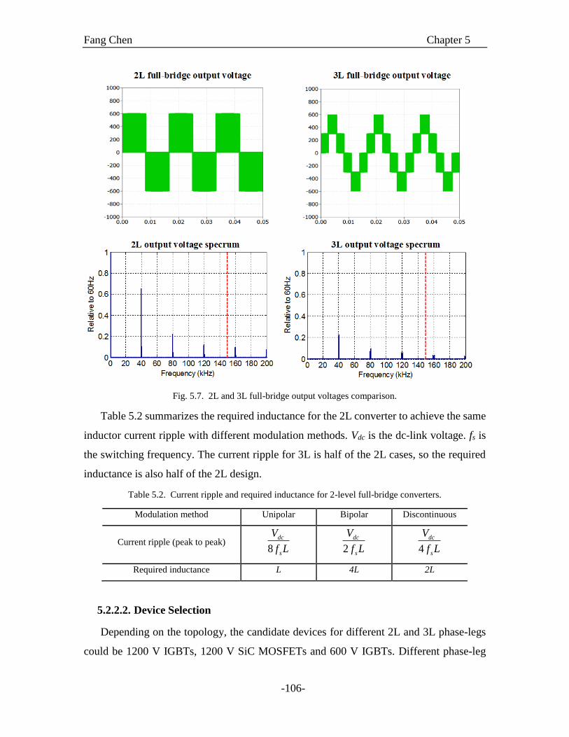
Fang Chen Chapter 5
-106-
Fig. 5.7. 2L and 3L full-bridge output voltages comparison.
Table 5.2 summarizes the required inductance for the 2L converter to achieve the same
inductor current ripple with different modulation methods. Vdc is the dc-link voltage. fs is
the switching frequency. The current ripple for 3L is half of the 2L cases, so the required
inductance is also half of the 2L design.
Table 5.2. Current ripple and required inductance for 2-level full-bridge converters.
Modulation method Unipolar Bipolar Discontinuous
Current ripple (peak to peak) 8
dc
s
V
f L
2
dc
s
V
f L
4
dc
s
V
f L
Required inductance L 4L 2L
5.2.2.2. Device Selection
Depending on the topology, the candidate devices for different 2L and 3L phase-legs
could be 1200 V IGBTs, 1200 V SiC MOSFETs and 600 V IGBTs. Different phase-leg
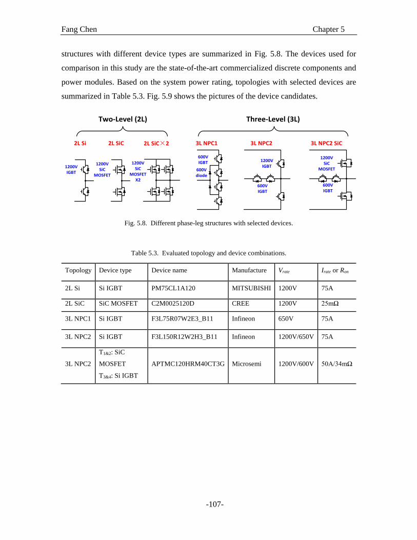
Fang Chen Chapter 5
-107-
structures with different device types are summarized in Fig. 5.8. The devices used for
comparison in this study are the state-of-the-art commercialized discrete components and
power modules. Based on the system power rating, topologies with selected devices are
summarized in Table 5.3. Fig. 5.9 shows the pictures of the device candidates.
1200V IGBT
1200VSiC
MOSFET
1200VSiC
MOSFETX2
600V IGBT
1200VSiC
MOSFET
600V IGBT
600V IGBT
1200V IGBT
2L Si 2L SiC 2L SiC×2 3L NPC1 3L NPC2 3L NPC2 SiC
Two-Level (2L) Three-Level (3L)
600V diode
Fig. 5.8. Different phase-leg structures with selected devices.
Table 5.3. Evaluated topology and device combinations.
Topology Device type Device name Manufacture Vrate Irate or Ron
2L Si Si IGBT PM75CL1A120 MITSUBISHI 1200V 75A
2L SiC SiC MOSFET C2M0025120D CREE 1200V 25mΩ
3L NPC1 Si IGBT F3L75R07W2E3_B11 Infineon 650V 75A
3L NPC2 Si IGBT F3L150R12W2H3_B11 Infineon 1200V/650V 75A
3L NPC2
T1&2: SiC
MOSFET
T3&4: Si IGBT
APTMC120HRM40CT3G Microsemi 1200V/600V 50A/34mΩ
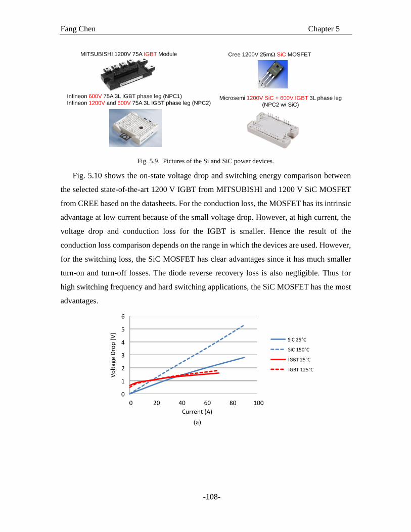
Fang Chen Chapter 5
-108-
MITSUBISHI 1200V 75A IGBT Module Cree 1200V 25mΩ SiC MOSFET
Infineon 600V 75A 3L IGBT phase leg (NPC1)
Infineon 1200V and 600V 75A 3L IGBT phase leg (NPC2)Microsemi 1200V SiC + 600V IGBT 3L phase leg
(NPC2 w/ SiC)
Fig. 5.9. Pictures of the Si and SiC power devices.
Fig. 5.10 shows the on-state voltage drop and switching energy comparison between
the selected state-of-the-art 1200 V IGBT from MITSUBISHI and 1200 V SiC MOSFET
from CREE based on the datasheets. For the conduction loss, the MOSFET has its intrinsic
advantage at low current because of the small voltage drop. However, at high current, the
voltage drop and conduction loss for the IGBT is smaller. Hence the result of the
conduction loss comparison depends on the range in which the devices are used. However,
for the switching loss, the SiC MOSFET has clear advantages since it has much smaller
turn-on and turn-off losses. The diode reverse recovery loss is also negligible. Thus for
high switching frequency and hard switching applications, the SiC MOSFET has the most
advantages.
0
1
2
3
4
5
6
0 20 40 60 80 100
Vo
ltag
e D
rop
(V
)
Current (A)
SiC 25°C
SiC 150°C
IGBT 25°C
IGBT 125°C
(a)
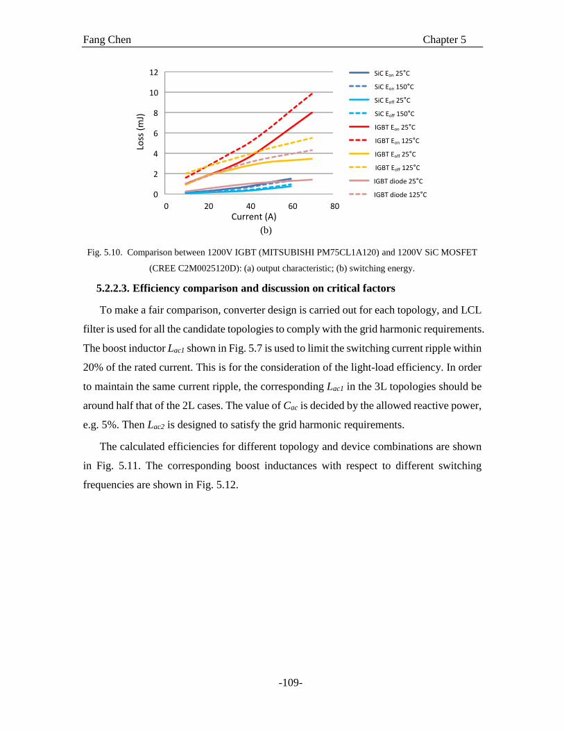
Fang Chen Chapter 5
-109-
0
2
4
6
8
10
12
0 20 40 60 80
Loss
(m
J)
Current (A)
SiC Eon 25°C
SiC Eon 150°C
SiC Eoff 25°C
SiC Eoff 150°C
IGBT Eon 25°C
IGBT Eon 125°C
IGBT Eoff 25°C
IGBT Eoff 125°C
IGBT diode 25°C
IGBT diode 125°C
(b)
Fig. 5.10. Comparison between 1200V IGBT (MITSUBISHI PM75CL1A120) and 1200V SiC MOSFET
(CREE C2M0025120D): (a) output characteristic; (b) switching energy.
5.2.2.3. Efficiency comparison and discussion on critical factors
To make a fair comparison, converter design is carried out for each topology, and LCL
filter is used for all the candidate topologies to comply with the grid harmonic requirements.
The boost inductor Lac1 shown in Fig. 5.7 is used to limit the switching current ripple within
20% of the rated current. This is for the consideration of the light-load efficiency. In order
to maintain the same current ripple, the corresponding Lac1 in the 3L topologies should be
around half that of the 2L cases. The value of Cac is decided by the allowed reactive power,
e.g. 5%. Then Lac2 is designed to satisfy the grid harmonic requirements.
The calculated efficiencies for different topology and device combinations are shown
in Fig. 5.11. The corresponding boost inductances with respect to different switching
frequencies are shown in Fig. 5.12.
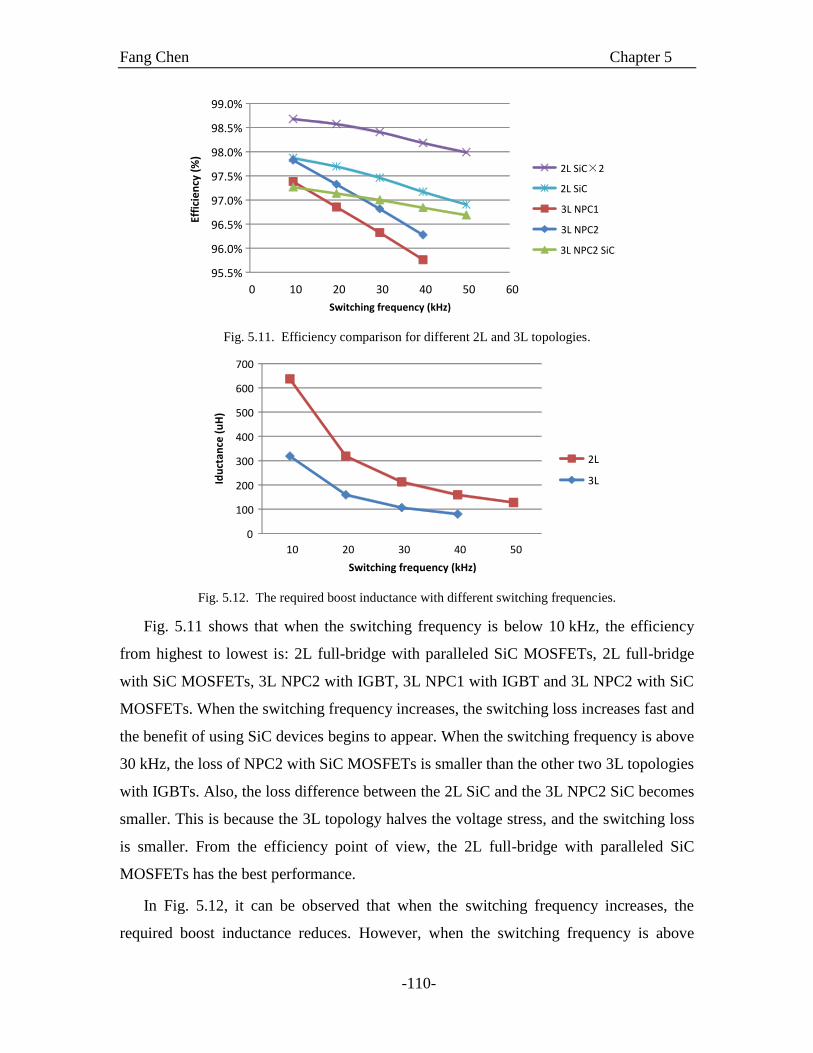
Fang Chen Chapter 5
-110-
95.5%
96.0%
96.5%
97.0%
97.5%
98.0%
98.5%
99.0%
0 10 20 30 40 50 60
Effi
cie
ncy
(%
)
Switching frequency (kHz)
2L SiC×2
2L SiC
3L NPC1
3L NPC2
3L NPC2 SiC
Fig. 5.11. Efficiency comparison for different 2L and 3L topologies.
0
100
200
300
400
500
600
700
10 20 30 40 50
Idu
ctan
ce (
uH
)
Switching frequency (kHz)
2L
3L
Fig. 5.12. The required boost inductance with different switching frequencies.
Fig. 5.11 shows that when the switching frequency is below 10 kHz, the efficiency
from highest to lowest is: 2L full-bridge with paralleled SiC MOSFETs, 2L full-bridge
with SiC MOSFETs, 3L NPC2 with IGBT, 3L NPC1 with IGBT and 3L NPC2 with SiC
MOSFETs. When the switching frequency increases, the switching loss increases fast and
the benefit of using SiC devices begins to appear. When the switching frequency is above
30 kHz, the loss of NPC2 with SiC MOSFETs is smaller than the other two 3L topologies
with IGBTs. Also, the loss difference between the 2L SiC and the 3L NPC2 SiC becomes
smaller. This is because the 3L topology halves the voltage stress, and the switching loss
is smaller. From the efficiency point of view, the 2L full-bridge with paralleled SiC
MOSFETs has the best performance.
In Fig. 5.12, it can be observed that when the switching frequency increases, the
required boost inductance reduces. However, when the switching frequency is above
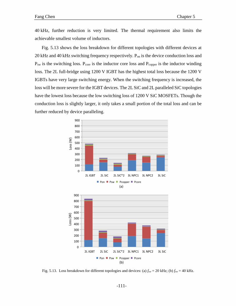
Fang Chen Chapter 5
-111-
40 kHz, further reduction is very limited. The thermal requirement also limits the
achievable smallest volume of inductors.
Fig. 5.13 shows the loss breakdown for different topologies with different devices at
20 kHz and 40 kHz switching frequency respectively. Pon is the device conduction loss and
Psw is the switching loss. Pcore is the inductor core loss and Pcopper is the inductor winding
loss. The 2L full-bridge using 1200 V IGBT has the highest total loss because the 1200 V
IGBTs have very large switching energy. When the switching frequency is increased, the
loss will be more severe for the IGBT devices. The 2L SiC and 2L paralleled SiC topologies
have the lowest loss because the low switching loss of 1200 V SiC MOSFETs. Though the
conduction loss is slightly larger, it only takes a small portion of the total loss and can be
further reduced by device paralleling.
0
100
200
300
400
500
600
700
800
900
2L IGBT 2L SiC 2L SiC*2 3L NPC1 3L NPC2 3L SiC
Loss
(W
)
Pon Psw Pcopper Pcore
(a)
0
100
200
300
400
500
600
700
800
900
2L IGBT 2L SiC 2L SiC*2 3L NPC1 3L NPC2 3L SiC
Loss
(W
)
Pon Psw Pcopper Pcore
(b)
Fig. 5.13. Loss breakdown for different topologies and devices: (a) fsw = 20 kHz; (b) fsw = 40 kHz.
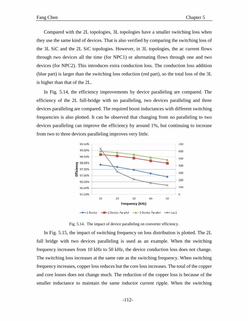
Fang Chen Chapter 5
-112-
Compared with the 2L topologies, 3L topologies have a smaller switching loss when
they use the same kind of devices. That is also verified by comparing the switching loss of
the 3L SiC and the 2L SiC topologies. However, in 3L topologies, the ac current flows
through two devices all the time (for NPC1) or alternating flows through one and two
devices (for NPC2). This introduces extra conduction loss. The conduction loss addition
(blue part) is larger than the switching loss reduction (red part), so the total loss of the 3L
is higher than that of the 2L.
In Fig. 5.14, the efficiency improvements by device paralleling are compared. The
efficiency of the 2L full-bridge with no paralleling, two devices paralleling and three
devices paralleling are compared. The required boost inductances with different switching
frequencies is also plotted. It can be observed that changing from no paralleling to two
devices paralleling can improve the efficiency by around 1%, but continuing to increase
from two to three devices paralleling improves very little.
Fig. 5.14. The impact of device paralleling on converter efficiency.
In Fig. 5.15, the impact of switching frequency on loss distribution is plotted. The 2L
full bridge with two devices paralleling is used as an example. When the switching
frequency increases from 10 kHz to 50 kHz, the device conduction loss does not change.
The switching loss increases at the same rate as the switching frequency. When switching
frequency increases, copper loss reduces but the core loss increases. The total of the copper
and core losses does not change much. The reduction of the copper loss is because of the
smaller inductance to maintain the same inductor current ripple. When the switching

Fang Chen Chapter 5
-113-
frequency is higher, the volume of the inductor is smaller and the total length and resistance
of the wire is also smaller.
Fig. 5.15. The impact of switching frequency on loss distribution.
In summary, the 2L full-bridge with two paralleled SiC MOSFETs working at 40 kHz
strikes a good balance between conduction and switching losses. Since interleaving has the
benefit of reduced size of passive components when compared with device paralleling.
Two phase interleaving is chosen as the final design to achieve high efficiency and power
density. The device used is the state-of-art commercialized SiC MOSFET C2M0025120D.
5.3. Power stage design
5.3.1. Pluggable phase-leg module design
Under interleaving, the converter requires a total of eight phase-legs. The concept of
modular design is adopted to achieve better maintainability and scalability. A pluggable
high-efficiency phase-leg card is designed as the basic unit to construct the whole converter.
Fig. 5.16 shows the components of each phase-leg card. Two isolated power supplies and
gate drivers are included into each card for the upper and lower devices of one phase-leg.
The gate driver ICs accept the PWM signals from the controller and drive the MOSFETs.
Besides the basic driving circuit, the card also includes the desaturation protection for over-
current and active clamping to prevent the false turn-on during switching transient. When
an error happens, the protection circuit turns off the driving signals and issues a fault signal
to notify the controller. Some small decoupling capacitors are put near the MOSFETs to
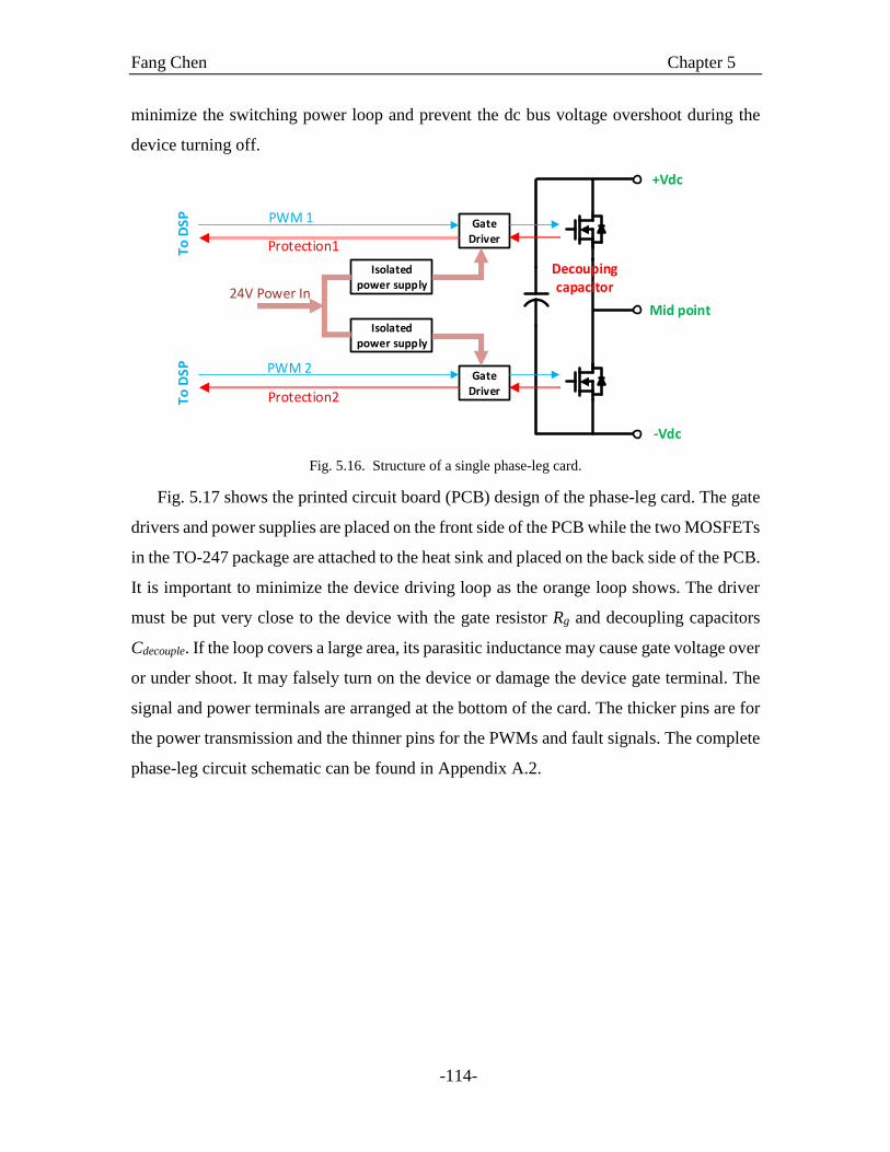
Fang Chen Chapter 5
-114-
minimize the switching power loop and prevent the dc bus voltage overshoot during the
device turning off.
Gate Driver
Isolated power supply
Gate Driver
Isolated power supply
PWM 1
PWM 2
Protection1
Protection2
24V Power In
+Vdc
-Vdc
Mid point
To
DS
PT
o D
SP
Decouping capacitor
Fig. 5.16. Structure of a single phase-leg card.
Fig. 5.17 shows the printed circuit board (PCB) design of the phase-leg card. The gate
drivers and power supplies are placed on the front side of the PCB while the two MOSFETs
in the TO-247 package are attached to the heat sink and placed on the back side of the PCB.
It is important to minimize the device driving loop as the orange loop shows. The driver
must be put very close to the device with the gate resistor Rg and decoupling capacitors
Cdecouple. If the loop covers a large area, its parasitic inductance may cause gate voltage over
or under shoot. It may falsely turn on the device or damage the device gate terminal. The
signal and power terminals are arranged at the bottom of the card. The thicker pins are for
the power transmission and the thinner pins for the PWMs and fault signals. The complete
phase-leg circuit schematic can be found in Appendix A.2.
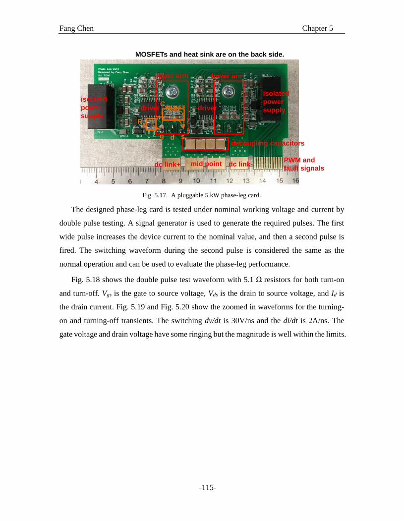
Fang Chen Chapter 5
-115-
MOSFETs and heat sink are on the back side.
upper arm lower arm
decoupling capacitors
dc link+ dc link-mid pointPWM and
fault signals
driver driver
isolated
power
supply
isolated
power
supply
Rg
Cdecouple
dg s
Fig. 5.17. A pluggable 5 kW phase-leg card.
The designed phase-leg card is tested under nominal working voltage and current by
double pulse testing. A signal generator is used to generate the required pulses. The first
wide pulse increases the device current to the nominal value, and then a second pulse is
fired. The switching waveform during the second pulse is considered the same as the
normal operation and can be used to evaluate the phase-leg performance.
Fig. 5.18 shows the double pulse test waveform with 5.1 Ω resistors for both turn-on
and turn-off. Vgs is the gate to source voltage, Vds is the drain to source voltage, and Id is
the drain current. Fig. 5.19 and Fig. 5.20 show the zoomed in waveforms for the turning-
on and turning-off transients. The switching dv/dt is 30V/ns and the di/dt is 2A/ns. The
gate voltage and drain voltage have some ringing but the magnitude is well within the limits.
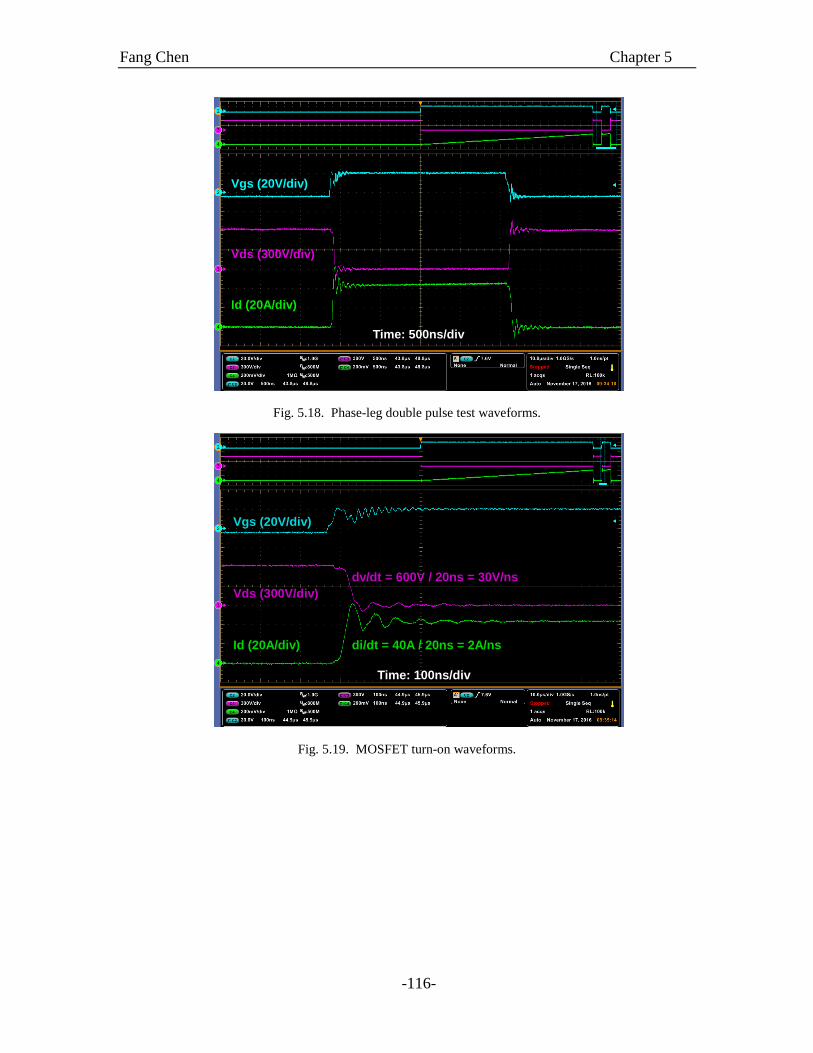
Fang Chen Chapter 5
-116-
Vgs (20V/div)
Vds (300V/div)
Id (20A/div)
Time: 500ns/div
Fig. 5.18. Phase-leg double pulse test waveforms.
Vgs (20V/div)
Vds (300V/div)
Id (20A/div)
Time: 100ns/div
dv/dt = 600V / 20ns = 30V/ns
di/dt = 40A / 20ns = 2A/ns
Fig. 5.19. MOSFET turn-on waveforms.
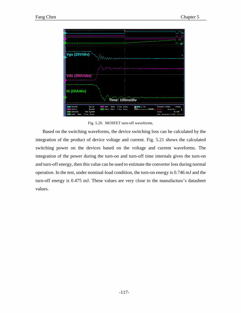
Fang Chen Chapter 5
-117-
Vgs (20V/div)
Vds (300V/div)
Id (20A/div)
Time: 100ns/div
Fig. 5.20. MOSFET turn-off waveforms.
Based on the switching waveforms, the device switching loss can be calculated by the
integration of the product of device voltage and current. Fig. 5.21 shows the calculated
switching power on the devices based on the voltage and current waveforms. The
integration of the power during the turn-on and turn-off time internals gives the turn-on
and turn-off energy, then this value can be used to estimate the converter loss during normal
operation. In the test, under nominal-load condition, the turn-on energy is 0.746 mJ and the
turn-off energy is 0.475 mJ. These values are very close to the manufacture’s datasheet
values.
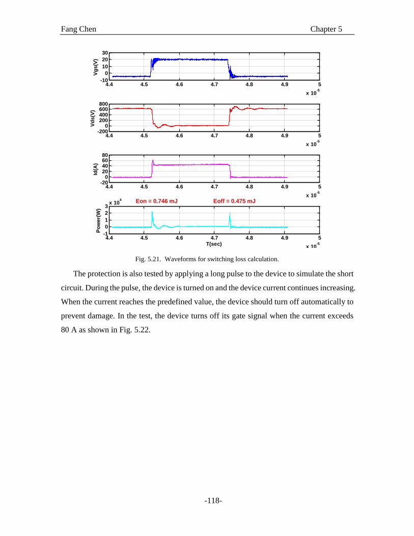
Fang Chen Chapter 5
-118-
4.4 4.5 4.6 4.7 4.8 4.9 5
x 10-5
-10
0
10
20
30
Vg
s(V
)
4.4 4.5 4.6 4.7 4.8 4.9 5
x 10-5
-2000
200400600800
Vd
s(V
)
4.4 4.5 4.6 4.7 4.8 4.9 5
x 10-5
-200
20406080
Id(A
)
4.4 4.5 4.6 4.7 4.8 4.9 5
x 10-5
-1
0
1
2
3x 10
4
Po
we
r(W
)
T(sec)
Eon = 0.746 mJ Eoff = 0.475 mJ
Fig. 5.21. Waveforms for switching loss calculation.
The protection is also tested by applying a long pulse to the device to simulate the short
circuit. During the pulse, the device is turned on and the device current continues increasing.
When the current reaches the predefined value, the device should turn off automatically to
prevent damage. In the test, the device turns off its gate signal when the current exceeds
80 A as shown in Fig. 5.22.
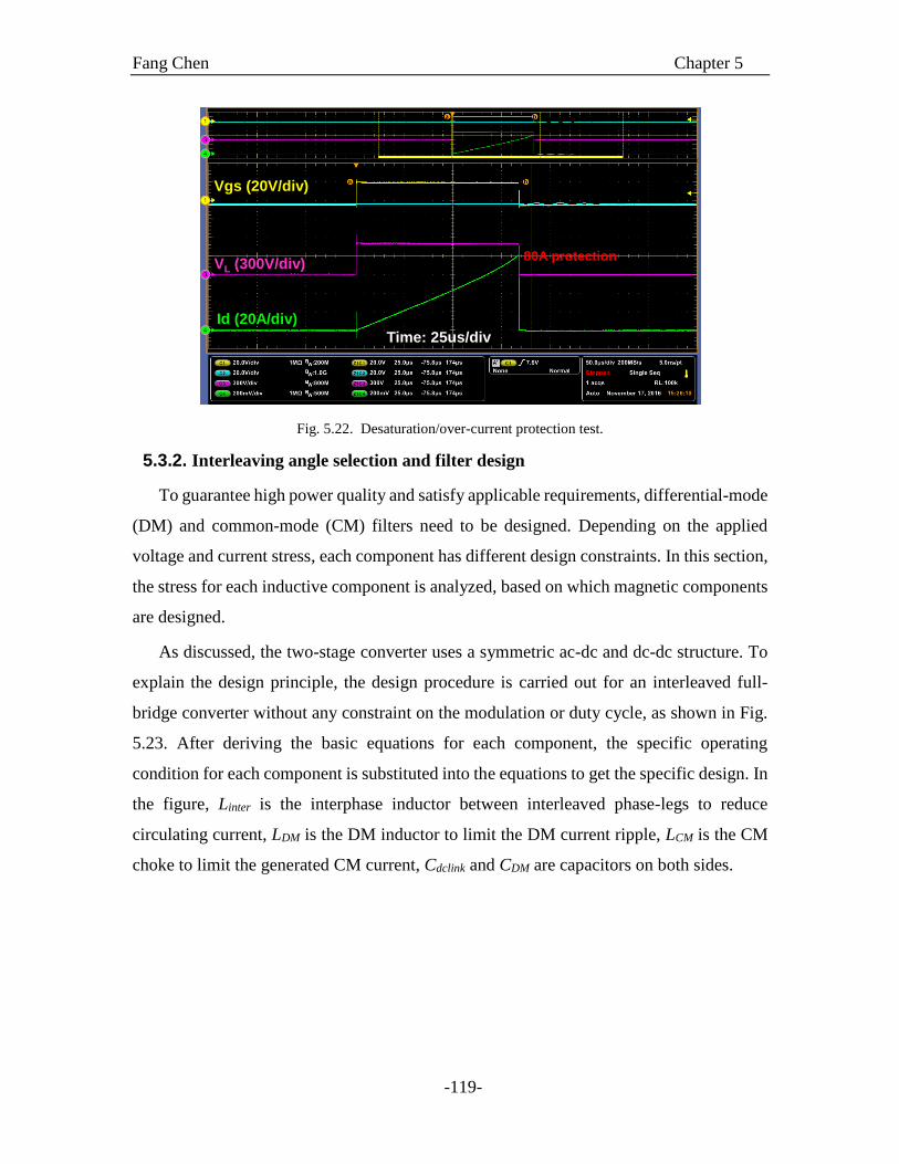
Fang Chen Chapter 5
-119-
Vgs (20V/div)
VL (300V/div)
Id (20A/div)
Time: 25us/div
80A protection
Fig. 5.22. Desaturation/over-current protection test.
5.3.2. Interleaving angle selection and filter design
To guarantee high power quality and satisfy applicable requirements, differential-mode
(DM) and common-mode (CM) filters need to be designed. Depending on the applied
voltage and current stress, each component has different design constraints. In this section,
the stress for each inductive component is analyzed, based on which magnetic components
are designed.
As discussed, the two-stage converter uses a symmetric ac-dc and dc-dc structure. To
explain the design principle, the design procedure is carried out for an interleaved full-
bridge converter without any constraint on the modulation or duty cycle, as shown in Fig.
5.23. After deriving the basic equations for each component, the specific operating
condition for each component is substituted into the equations to get the specific design. In
the figure, Linter is the interphase inductor between interleaved phase-legs to reduce
circulating current, LDM is the DM inductor to limit the DM current ripple, LCM is the CM
choke to limit the generated CM current, Cdclink and CDM are capacitors on both sides.
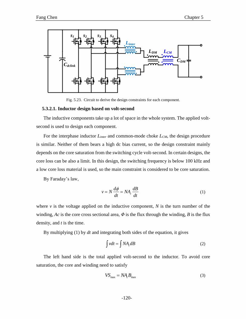
Fang Chen Chapter 5
-120-
Linter
LDM LCM
CDMCdclink
s1 s2 s3 s4
Fig. 5.23. Circuit to derive the design constraints for each component.
5.3.2.1. Inductor design based on volt-second
The inductive components take up a lot of space in the whole system. The applied volt-
second is used to design each component.
For the interphase inductor Linter and common-mode choke LCM, the design procedure
is similar. Neither of them bears a high dc bias current, so the design constraint mainly
depends on the core saturation from the switching cycle volt-second. In certain designs, the
core loss can be also a limit. In this design, the switching frequency is below 100 kHz and
a low core loss material is used, so the main constraint is considered to be core saturation.
By Faraday’s law,
c
d dBv N NA
dt dt
(1)
where v is the voltage applied on the inductive component, N is the turn number of the
winding, Ac is the core cross sectional area, Φ is the flux through the winding, B is the flux
density, and t is the time.
By multiplying (1) by dt and integrating both sides of the equation, it gives
cvdt NA dB (2)
The left hand side is the total applied volt-second to the inductor. To avoid core
saturation, the core and winding need to satisfy
max maxcVS NA B (3)

Fang Chen Chapter 5
-121-
where VSmax is the applied maximum volt-second during every switching cycle, Bmax is the
allowed maximum flux density for the core material.
Then the size of the inductor can be expressed as
max
max
c
VSNA
B (4)
or in the area product form
max
max
rmsa c
u
I VSW A
J K B
(5)
where Wa is the window area of the core, Irms is the rms value of the conducted current
through the winding, J is the current density for the wire, and Ku is the filling factor of the
core window area.
For the DM inductor, usually the maximum current going through the inductor decides
the maximum flux density and thus the volume, which means
max
max
c
L INA
B
(6)
where L is the inductance value and Imax is the maximum inductor current.
Since the current is decided by the load, if L is designed based on the maximum
inductor current ripple ΔImax due to light-load efficiency considerations, then the inductor
value satisfies:
max
max
VSL
I
(7)
The inductor volume can be also expressed in the form of volt-second
max max
max max
c
VS INA
B I
(8)
or
max max
max max
rmsa c
u
I VS IW A
J K B I
(9)
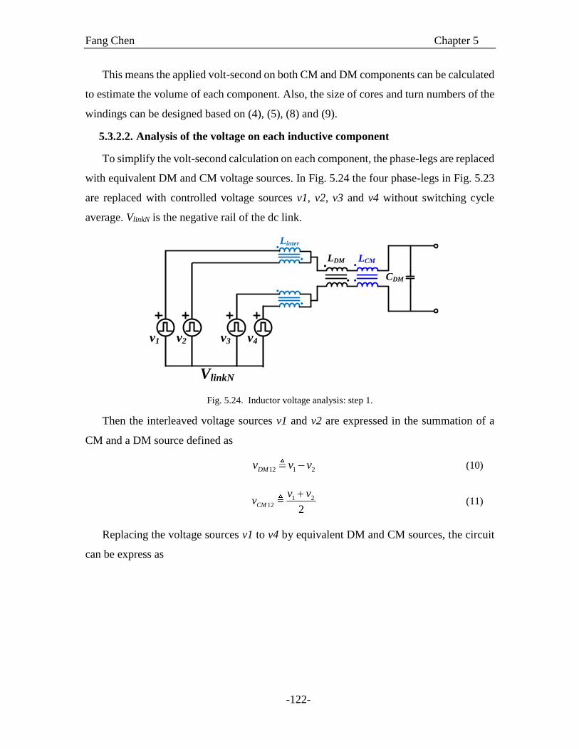
Fang Chen Chapter 5
-122-
This means the applied volt-second on both CM and DM components can be calculated
to estimate the volume of each component. Also, the size of cores and turn numbers of the
windings can be designed based on (4), (5), (8) and (9).
5.3.2.2. Analysis of the voltage on each inductive component
To simplify the volt-second calculation on each component, the phase-legs are replaced
with equivalent DM and CM voltage sources. In Fig. 5.24 the four phase-legs in Fig. 5.23
are replaced with controlled voltage sources v1, v2, v3 and v4 without switching cycle
average. VlinkN is the negative rail of the dc link.
Linter
LDM LCM
CDM
v4v3v2v1
VlinkN
Fig. 5.24. Inductor voltage analysis: step 1.
Then the interleaved voltage sources v1 and v2 are expressed in the summation of a
CM and a DM source defined as
12 1 2DMv v v (10)
1 212
2CM
v vv
(11)
Replacing the voltage sources v1 to v4 by equivalent DM and CM sources, the circuit
can be express as
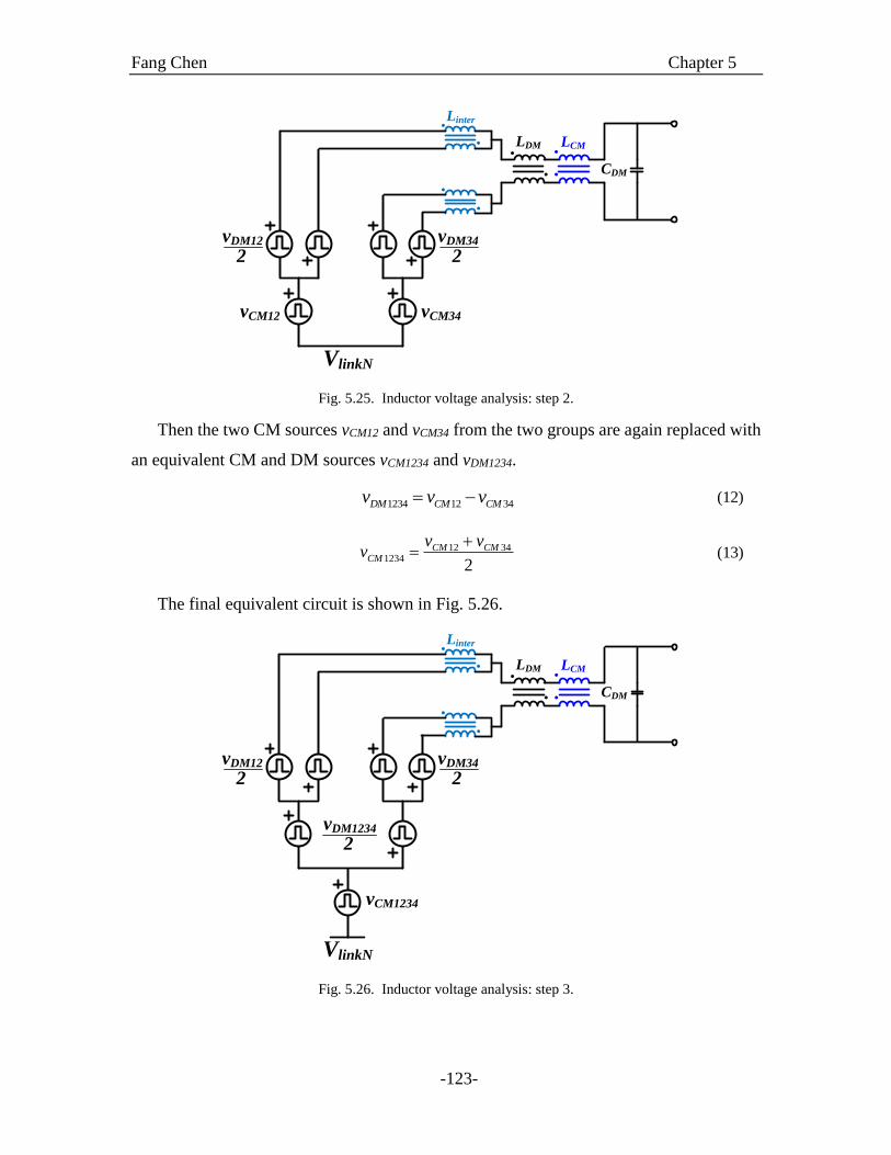
Fang Chen Chapter 5
-123-
Linter
LDM LCM
CDM
VlinkN
vCM12 vCM34
vDM12
2vDM34
2
Fig. 5.25. Inductor voltage analysis: step 2.
Then the two CM sources vCM12 and vCM34 from the two groups are again replaced with
an equivalent CM and DM sources vCM1234 and vDM1234.
1234 12 34DM CM CMv v v (12)
12 341234
2
CM CMCM
v vv
(13)
The final equivalent circuit is shown in Fig. 5.26.
Linter
LDM LCM
CDM
VlinkN
vDM12
2vDM34
2
vDM1234
2
vCM1234
Fig. 5.26. Inductor voltage analysis: step 3.

Fang Chen Chapter 5
-124-
If the circuit is balanced, then the DM and CM quantities are not coupled. The
switching cycle pulsating voltage applied on each component can be expressed as
12interL DMv v (14)
1234DML DMv v (15)
1234CML CMv v (16)
It is worth noting that these equations are only valid for switching cycle volt-second
analysis. The voltage appearing on the ac port will also influence the voltage waveform on
LDM. However, since this voltage is usually at low frequency, it will not influence the
switching cycle flux swing. Also, the voltage applied on LCM could be smaller than the
calculated value depending on how the power stage is grounded. However, this equation
shows the worst case where all the voltage is applied on the choke LCM. If LCM is designed
based on this criterion, it has the capability to work with flexible grounding schemes.
5.3.2.3. Effect of interleaving on volt-second
In general, the four interleaved phase-legs can be divided into two groups. The
interleaved phase-legs s1 and s2 are in one group; s3 and s4 are in the other group. Within
each group, the two phase-legs share the same duty cycle. If the duty cycles are considered
symmetric around 0.5 for the two groups, i.e. the duty cycles are 0.5+d/2 and 0.5-d/2
respectively, then the sum of the two duty cycles is always equal to one.
When the two groups of phase-legs are not phase shifted, the PWM signals for the four
phase-legs are drawn in Fig. 5.27. In the example, the driving signals for the upper switches
during one switching cycle are drawn. The driving signals for the lower switches are
complementary to the upper devices. The duty cycle is 0.8 for s1 and s2, 0.2 for s3 and s4.
When there is not phase shift, they are all center aligned.
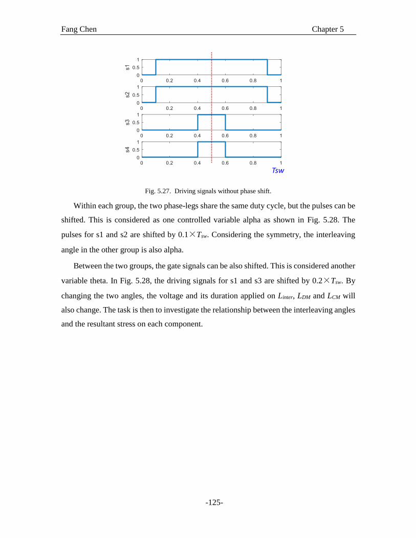
Fang Chen Chapter 5
-125-
Tsw
Fig. 5.27. Driving signals without phase shift.
Within each group, the two phase-legs share the same duty cycle, but the pulses can be
shifted. This is considered as one controlled variable alpha as shown in Fig. 5.28. The
pulses for s1 and s2 are shifted by 0.1×Tsw. Considering the symmetry, the interleaving
angle in the other group is also alpha.
Between the two groups, the gate signals can be also shifted. This is considered another
variable theta. In Fig. 5.28, the driving signals for s1 and s3 are shifted by 0.2×Tsw. By
changing the two angles, the voltage and its duration applied on Linter, LDM and LCM will
also change. The task is then to investigate the relationship between the interleaving angles
and the resultant stress on each component.
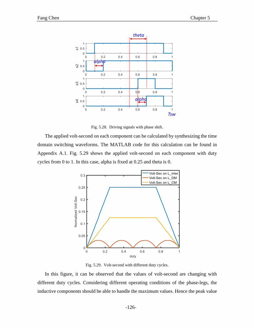
Fang Chen Chapter 5
-126-
alpha
alpha
theta
Tsw
Fig. 5.28. Driving signals with phase shift.
The applied volt-second on each component can be calculated by synthesizing the time
domain switching waveforms. The MATLAB code for this calculation can be found in
Appendix A.1. Fig. 5.29 shows the applied volt-second on each component with duty
cycles from 0 to 1. In this case, alpha is fixed at 0.25 and theta is 0.
Fig. 5.29. Volt-second with different duty cycles.
In this figure, it can be observed that the values of volt-second are changing with
different duty cycles. Considering different operating conditions of the phase-legs, the
inductive components should be able to handle the maximum values. Hence the peak value
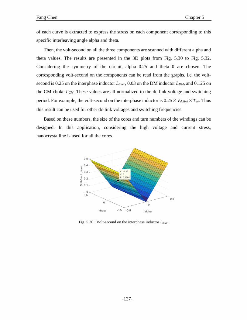
Fang Chen Chapter 5
-127-
of each curve is extracted to express the stress on each component corresponding to this
specific interleaving angle alpha and theta.
Then, the volt-second on all the three components are scanned with different alpha and
theta values. The results are presented in the 3D plots from Fig. 5.30 to Fig. 5.32.
Considering the symmetry of the circuit, alpha=0.25 and theta=0 are chosen. The
corresponding volt-second on the components can be read from the graphs, i.e. the volt-
second is 0.25 on the interphase inductor Linter, 0.03 on the DM inductor LDM, and 0.125 on
the CM choke LCM. These values are all normalized to the dc link voltage and switching
period. For example, the volt-second on the interphase inductor is 0.25×Vdclink×Tsw. Thus
this result can be used for other dc-link voltages and switching frequencies.
Based on these numbers, the size of the cores and turn numbers of the windings can be
designed. In this application, considering the high voltage and current stress,
nanocrystalline is used for all the cores.
Fig. 5.30. Volt-second on the interphase inductor Linter.
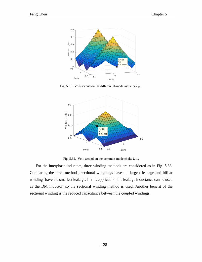
Fang Chen Chapter 5
-128-
Fig. 5.31. Volt-second on the differential-mode inductor LDM.
Fig. 5.32. Volt-second on the common-mode choke LCM.
For the interphase inductors, three winding methods are considered as in Fig. 5.33.
Comparing the three methods, sectional wingdings have the largest leakage and bifilar
windings have the smallest leakage. In this application, the leakage inductance can be used
as the DM inductor, so the sectional winding method is used. Another benefit of the
sectional winding is the reduced capacitance between the coupled windings.

Fang Chen Chapter 5
-129-
Lcouple = 18mH
Lleak = 11uH
Lcouple = 63mH
Lleak = 1.8uH
Lcouple = 46mH
Lleak = 0.42uH
sectional double layer bifilar
Fig. 5.33. Interphase inductor with different winding placements.
The CM choke is designed in a similar way as the interphase inductor except that the
conducted current is doubled so the winding wire size needs to be doubled as well. For the
DM inductor, an air gap is added to store the energy and adjust the inductance. To reduce
the high-frequency winding resistance, Litz wires are used for all the inductors. The final
ac and dc component parameters are listed in Table 5.4. The meaning of each symbol can
be found in the complete circuit schematic shown in Fig. 5.42.
Table 5.4. DM and CM filter parameters.
Symbol Value
AC filters
Li_ac 18 mH
LD_ac 187 μH
LC_ac 3 mH
CD_ac 20 μF
RD_ac 1 Ω
CC_ac 10 nF
DC filters
Li_dc 62 mH
LD_dc 160 μH
LC_dc 4.9 mH
CD_dc 10 μF
RD_dc 1 Ω
CC_dc 100 nF
RGND 100 kΩ
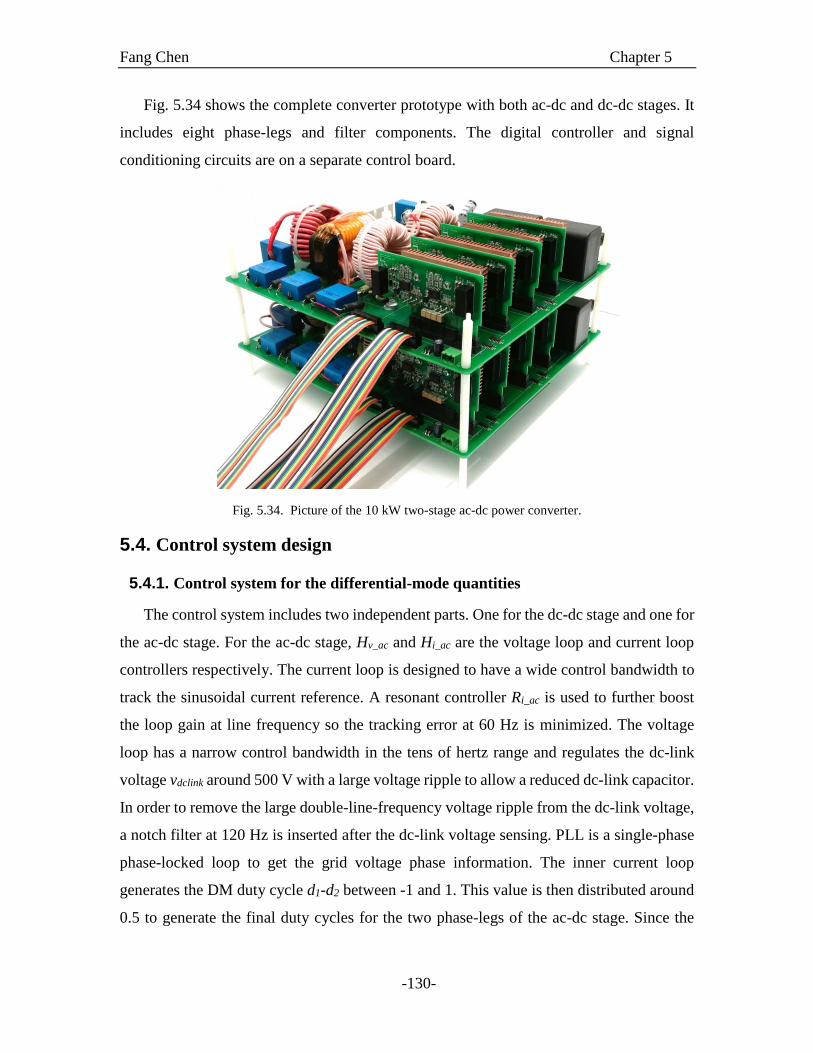
Fang Chen Chapter 5
-130-
Fig. 5.34 shows the complete converter prototype with both ac-dc and dc-dc stages. It
includes eight phase-legs and filter components. The digital controller and signal
conditioning circuits are on a separate control board.
Fig. 5.34. Picture of the 10 kW two-stage ac-dc power converter.
5.4. Control system design
5.4.1. Control system for the differential-mode quantities
The control system includes two independent parts. One for the dc-dc stage and one for
the ac-dc stage. For the ac-dc stage, Hv_ac and Hi_ac are the voltage loop and current loop
controllers respectively. The current loop is designed to have a wide control bandwidth to
track the sinusoidal current reference. A resonant controller Ri_ac is used to further boost
the loop gain at line frequency so the tracking error at 60 Hz is minimized. The voltage
loop has a narrow control bandwidth in the tens of hertz range and regulates the dc-link
voltage vdclink around 500 V with a large voltage ripple to allow a reduced dc-link capacitor.
In order to remove the large double-line-frequency voltage ripple from the dc-link voltage,
a notch filter at 120 Hz is inserted after the dc-link voltage sensing. PLL is a single-phase
phase-locked loop to get the grid voltage phase information. The inner current loop
generates the DM duty cycle d1-d2 between -1 and 1. This value is then distributed around
0.5 to generate the final duty cycles for the two phase-legs of the ac-dc stage. Since the
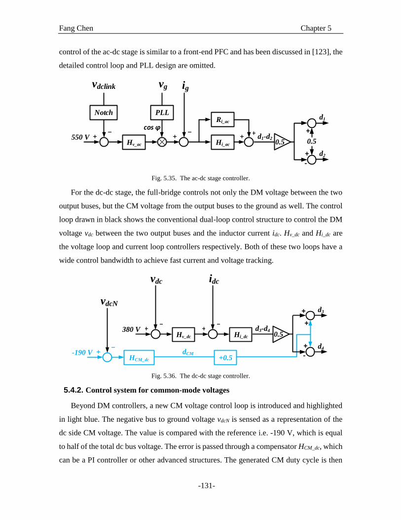
Fang Chen Chapter 5
-131-
control of the ac-dc stage is similar to a front-end PFC and has been discussed in [123], the
detailed control loop and PLL design are omitted.
550 VHv_ac Hi_ac
PLL
cos ϕ
d2
d1-d2
-+
0.5
+
0.5
d1
vgvdclink ig
NotchRi_ac
Fig. 5.35. The ac-dc stage controller.
For the dc-dc stage, the full-bridge controls not only the DM voltage between the two
output buses, but the CM voltage from the output buses to the ground as well. The control
loop drawn in black shows the conventional dual-loop control structure to control the DM
voltage vdc between the two output buses and the inductor current idc. Hv_dc and Hi_dc are
the voltage loop and current loop controllers respectively. Both of these two loops have a
wide control bandwidth to achieve fast current and voltage tracking.
380 VHv_dc
-190 VHCM_dc
Hi_dc
d3-d4
dCM
d3
d4
-+
+
+
0.5
+0.5
vdcN
vdc idc
Fig. 5.36. The dc-dc stage controller.
5.4.2. Control system for common-mode voltages
Beyond DM controllers, a new CM voltage control loop is introduced and highlighted
in light blue. The negative bus to ground voltage vdcN is sensed as a representation of the
dc side CM voltage. The value is compared with the reference i.e. -190 V, which is equal
to half of the total dc bus voltage. The error is passed through a compensator HCM_dc, which
can be a PI controller or other advanced structures. The generated CM duty cycle is then
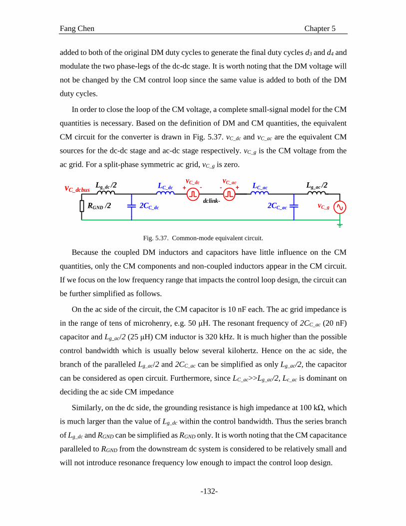
Fang Chen Chapter 5
-132-
added to both of the original DM duty cycles to generate the final duty cycles d3 and d4 and
modulate the two phase-legs of the dc-dc stage. It is worth noting that the DM voltage will
not be changed by the CM control loop since the same value is added to both of the DM
duty cycles.
In order to close the loop of the CM voltage, a complete small-signal model for the CM
quantities is necessary. Based on the definition of DM and CM quantities, the equivalent
CM circuit for the converter is drawn in Fig. 5.37. vC_dc and vC_ac are the equivalent CM
sources for the dc-dc stage and ac-dc stage respectively. vC_g is the CM voltage from the
ac grid. For a split-phase symmetric ac grid, vC_g is zero.
LC_ac Lg_ac /2
vC_g
- +Lg_dc /2
RGND /2
- +LC_dc
vC_ac vC_dc
dclink-
vC_dcbus
2CC_ac2CC_dc
Fig. 5.37. Common-mode equivalent circuit.
Because the coupled DM inductors and capacitors have little influence on the CM
quantities, only the CM components and non-coupled inductors appear in the CM circuit.
If we focus on the low frequency range that impacts the control loop design, the circuit can
be further simplified as follows.
On the ac side of the circuit, the CM capacitor is 10 nF each. The ac grid impedance is
in the range of tens of microhenry, e.g. 50 μH. The resonant frequency of 2CC_ac (20 nF)
capacitor and Lg_ac/2 (25 μH) CM inductor is 320 kHz. It is much higher than the possible
control bandwidth which is usually below several kilohertz. Hence on the ac side, the
branch of the paralleled Lg_ac/2 and 2CC_ac can be simplified as only Lg_ac/2, the capacitor
can be considered as open circuit. Furthermore, since LC_ac>>Lg_ac/2, Lc_ac is dominant on
deciding the ac side CM impedance
Similarly, on the dc side, the grounding resistance is high impedance at 100 kΩ, which
is much larger than the value of Lg_dc within the control bandwidth. Thus the series branch
of Lg_dc and RGND can be simplified as RGND only. It is worth noting that the CM capacitance
paralleled to RGND from the downstream dc system is considered to be relatively small and
will not introduce resonance frequency low enough to impact the control loop design.
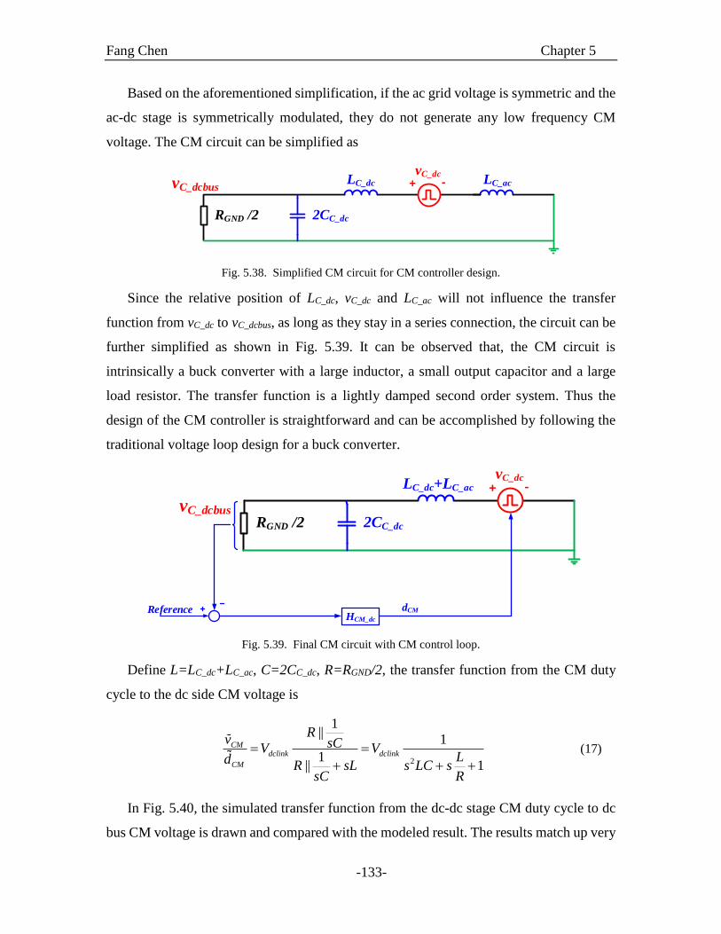
Fang Chen Chapter 5
-133-
Based on the aforementioned simplification, if the ac grid voltage is symmetric and the
ac-dc stage is symmetrically modulated, they do not generate any low frequency CM
voltage. The CM circuit can be simplified as
LC_ac
RGND /2
- +LC_dc
vC_dc
vC_dcbus
2CC_dc
Fig. 5.38. Simplified CM circuit for CM controller design.
Since the relative position of LC_dc, vC_dc and LC_ac will not influence the transfer
function from vC_dc to vC_dcbus, as long as they stay in a series connection, the circuit can be
further simplified as shown in Fig. 5.39. It can be observed that, the CM circuit is
intrinsically a buck converter with a large inductor, a small output capacitor and a large
load resistor. The transfer function is a lightly damped second order system. Thus the
design of the CM controller is straightforward and can be accomplished by following the
traditional voltage loop design for a buck converter.
RGND /2
- +LC_dc+LC_ac
vC_dc
vC_dcbus2CC_dc
ReferenceHCM_dc
dCM
Fig. 5.39. Final CM circuit with CM control loop.
Define L=LC_dc+LC_ac, C=2CC_dc, R=RGND/2, the transfer function from the CM duty
cycle to the dc side CM voltage is
2
1||
1
1|| 1
CMdclink dclink
CM
Rv sCV V
Ld R sL s LC ssC R
(17)
In Fig. 5.40, the simulated transfer function from the dc-dc stage CM duty cycle to dc
bus CM voltage is drawn and compared with the modeled result. The results match up very
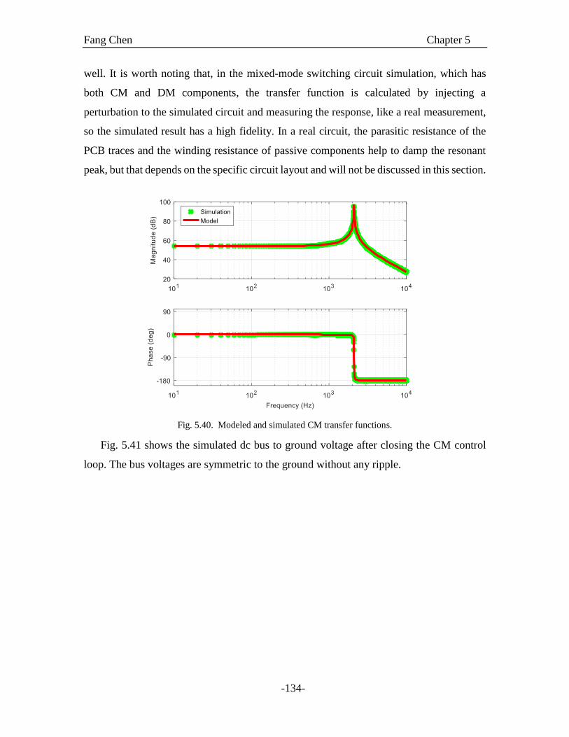
Fang Chen Chapter 5
-134-
well. It is worth noting that, in the mixed-mode switching circuit simulation, which has
both CM and DM components, the transfer function is calculated by injecting a
perturbation to the simulated circuit and measuring the response, like a real measurement,
so the simulated result has a high fidelity. In a real circuit, the parasitic resistance of the
PCB traces and the winding resistance of passive components help to damp the resonant
peak, but that depends on the specific circuit layout and will not be discussed in this section.
Fig. 5.40. Modeled and simulated CM transfer functions.
Fig. 5.41 shows the simulated dc bus to ground voltage after closing the CM control
loop. The bus voltages are symmetric to the ground without any ripple.
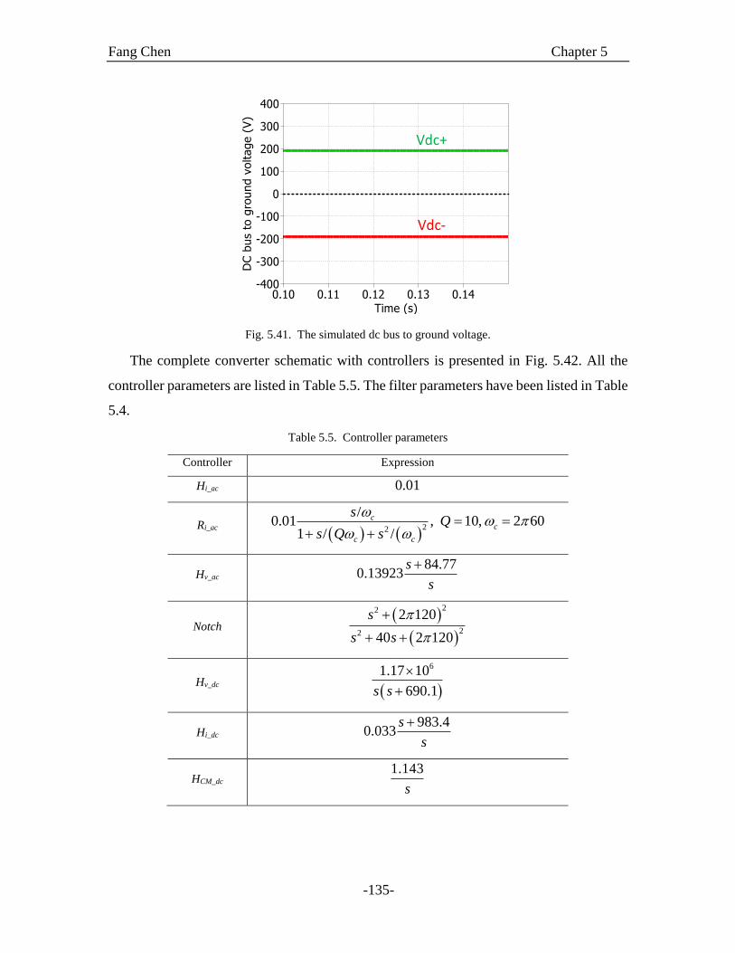
Fang Chen Chapter 5
-135-
Vdc+
Vdc-
Fig. 5.41. The simulated dc bus to ground voltage.
The complete converter schematic with controllers is presented in Fig. 5.42. All the
controller parameters are listed in Table 5.5. The filter parameters have been listed in Table
5.4.
Table 5.5. Controller parameters
Controller Expression
Hi_ac 0.01
Ri_ac
22
/0.01 , 10, 2 60
1 / /
cc
c c
sQ
s Q s
Hv_ac 84.77
0.13923s
s
Notch
22
22
2 120
40 2 120
s
s s
Hv_dc
61.17 10
690.1s s
Hi_dc 983.4
0.033s
s
HCM_dc 1.143
s
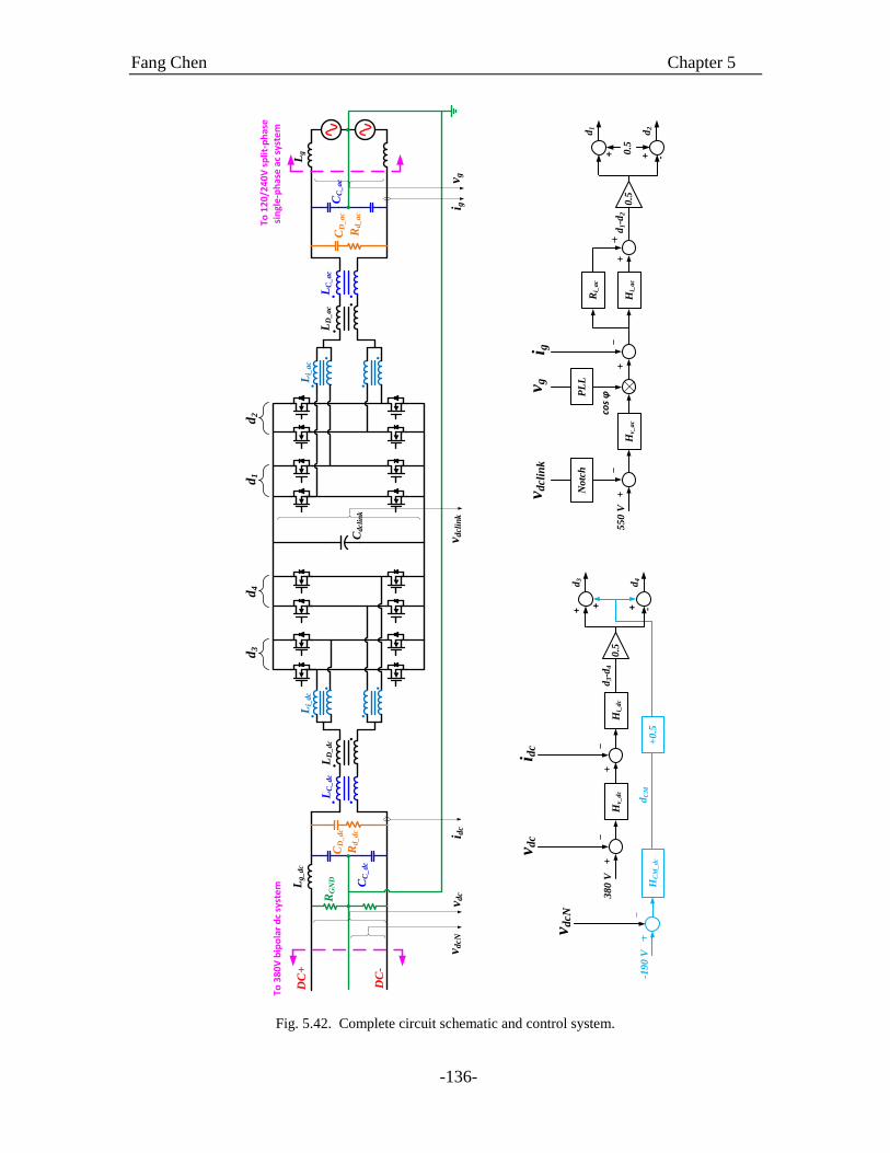
Fang Chen Chapter 5
-136-
Li_
ac
Li_
dc
LD
_dc
LC
_dc
LD
_ac
LC
_ac
DC
+
DC
-
To
12
0/2
40
V s
plit
-ph
ase
si
ngl
e-p
has
e a
c sy
ste
mTo
38
0V
bip
ola
r d
c sy
ste
m
CD
_dc
Rd
_dc
CC
_dc
CC
_ac
RG
ND
CD
_ac
Rd
_ac
Cdcl
ink
v dcl
ink
v dc
v dcN
v gi g
Lg
_dc
Lg
i dc
d1
d2
d3
d4
38
0 V
Hv_
dc
-19
0 V
HC
M_
dc
Hi_
dc
d3-d
4
dC
M
d3
d4
-+++
0.5
+0
.5
v dcN
v dc
i dc
55
0 V
Hv_
ac
Hi_
ac
PL
L
cos ϕ
d2
d1-d
2
-+0.5
+
0.5
d1
v gv d
clin
ki g
No
tch
Ri_
ac
Fig. 5.42. Complete circuit schematic and control system.
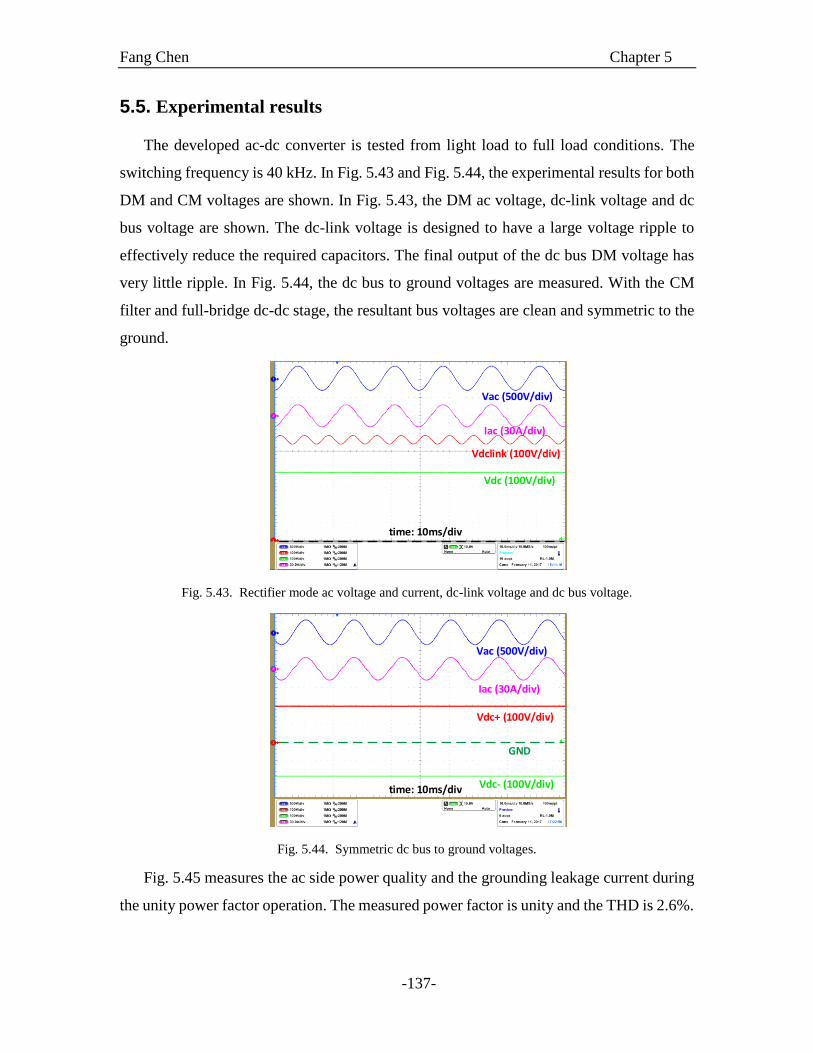
Fang Chen Chapter 5
-137-
5.5. Experimental results
The developed ac-dc converter is tested from light load to full load conditions. The
switching frequency is 40 kHz. In Fig. 5.43 and Fig. 5.44, the experimental results for both
DM and CM voltages are shown. In Fig. 5.43, the DM ac voltage, dc-link voltage and dc
bus voltage are shown. The dc-link voltage is designed to have a large voltage ripple to
effectively reduce the required capacitors. The final output of the dc bus DM voltage has
very little ripple. In Fig. 5.44, the dc bus to ground voltages are measured. With the CM
filter and full-bridge dc-dc stage, the resultant bus voltages are clean and symmetric to the
ground.
Vac (500V/div)
Iac (30A/div)
Vdc (100V/div)
Vdclink (100V/div)
time: 10ms/div
Fig. 5.43. Rectifier mode ac voltage and current, dc-link voltage and dc bus voltage.
Vac (500V/div)
Iac (30A/div)
Vdc- (100V/div)
Vdc+ (100V/div)
GND
time: 10ms/div
Fig. 5.44. Symmetric dc bus to ground voltages.
Fig. 5.45 measures the ac side power quality and the grounding leakage current during
the unity power factor operation. The measured power factor is unity and the THD is 2.6%.
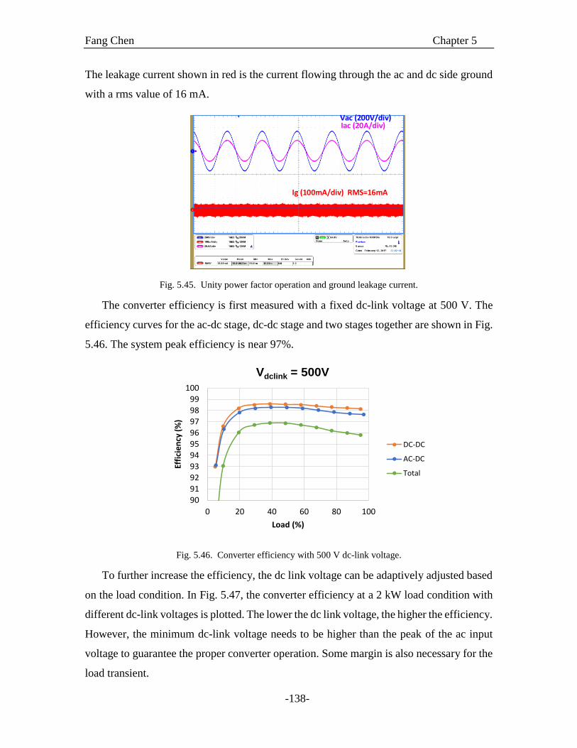
Fang Chen Chapter 5
-138-
The leakage current shown in red is the current flowing through the ac and dc side ground
with a rms value of 16 mA.
Fig. 5.45. Unity power factor operation and ground leakage current.
The converter efficiency is first measured with a fixed dc-link voltage at 500 V. The
efficiency curves for the ac-dc stage, dc-dc stage and two stages together are shown in Fig.
5.46. The system peak efficiency is near 97%.
Vdclink = 500V
90
91
92
93
94
95
96
97
98
99
100
0 20 40 60 80 100
Effi
cien
cy (
%)
Load (%)
DC-DC
AC-DC
Total
Fig. 5.46. Converter efficiency with 500 V dc-link voltage.
To further increase the efficiency, the dc link voltage can be adaptively adjusted based
on the load condition. In Fig. 5.47, the converter efficiency at a 2 kW load condition with
different dc-link voltages is plotted. The lower the dc link voltage, the higher the efficiency.
However, the minimum dc-link voltage needs to be higher than the peak of the ac input
voltage to guarantee the proper converter operation. Some margin is also necessary for the
load transient.
Vac (200V/div)Iac (20A/div)
Ig (100mA/div) RMS=16mA
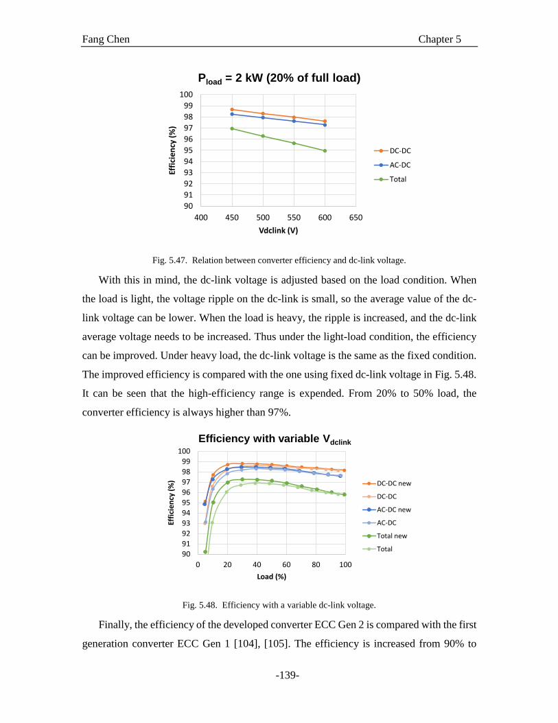
Fang Chen Chapter 5
-139-
Pload = 2 kW (20% of full load)
90
91
92
93
94
95
96
97
98
99
100
400 450 500 550 600 650
Effi
cie
ncy
(%
)
Vdclink (V)
DC-DC
AC-DC
Total
Fig. 5.47. Relation between converter efficiency and dc-link voltage.
With this in mind, the dc-link voltage is adjusted based on the load condition. When
the load is light, the voltage ripple on the dc-link is small, so the average value of the dc-
link voltage can be lower. When the load is heavy, the ripple is increased, and the dc-link
average voltage needs to be increased. Thus under the light-load condition, the efficiency
can be improved. Under heavy load, the dc-link voltage is the same as the fixed condition.
The improved efficiency is compared with the one using fixed dc-link voltage in Fig. 5.48.
It can be seen that the high-efficiency range is expended. From 20% to 50% load, the
converter efficiency is always higher than 97%.
Efficiency with variable Vdclink
90
91
92
93
94
95
96
97
98
99
100
0 20 40 60 80 100
Effi
cien
cy (
%)
Load (%)
DC-DC new
DC-DC
AC-DC new
AC-DC
Total new
Total
Fig. 5.48. Efficiency with a variable dc-link voltage.
Finally, the efficiency of the developed converter ECC Gen 2 is compared with the first
generation converter ECC Gen 1 [104], [105]. The efficiency is increased from 90% to
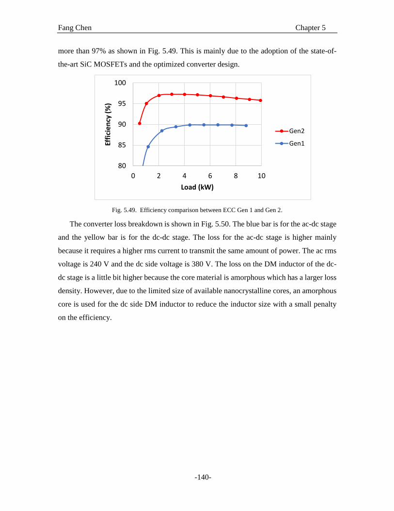
Fang Chen Chapter 5
-140-
more than 97% as shown in Fig. 5.49. This is mainly due to the adoption of the state-of-
the-art SiC MOSFETs and the optimized converter design.
Fig. 5.49. Efficiency comparison between ECC Gen 1 and Gen 2.
The converter loss breakdown is shown in Fig. 5.50. The blue bar is for the ac-dc stage
and the yellow bar is for the dc-dc stage. The loss for the ac-dc stage is higher mainly
because it requires a higher rms current to transmit the same amount of power. The ac rms
voltage is 240 V and the dc side voltage is 380 V. The loss on the DM inductor of the dc-
dc stage is a little bit higher because the core material is amorphous which has a larger loss
density. However, due to the limited size of available nanocrystalline cores, an amorphous
core is used for the dc side DM inductor to reduce the inductor size with a small penalty
on the efficiency.
80
85
90
95
100
0 2 4 6 8 10
Effi
cien
cy (
%)
Load (kW)
Gen2
Gen1
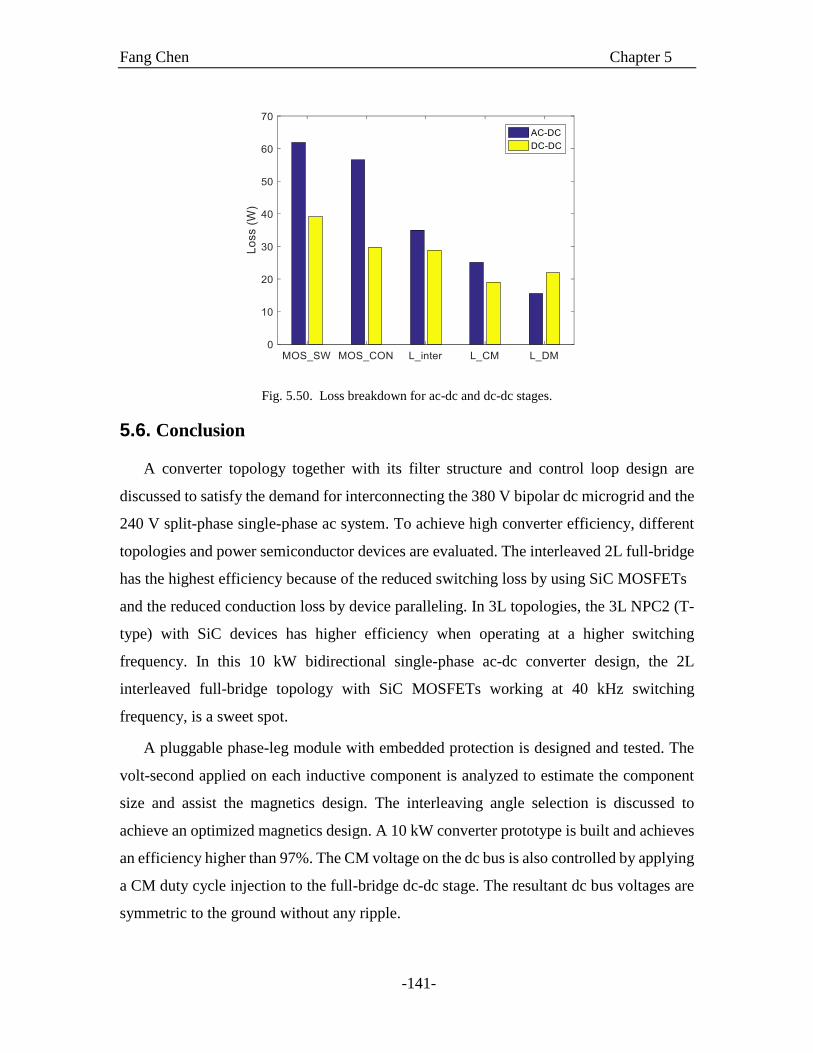
Fang Chen Chapter 5
-141-
Fig. 5.50. Loss breakdown for ac-dc and dc-dc stages.
5.6. Conclusion
A converter topology together with its filter structure and control loop design are
discussed to satisfy the demand for interconnecting the 380 V bipolar dc microgrid and the
240 V split-phase single-phase ac system. To achieve high converter efficiency, different
topologies and power semiconductor devices are evaluated. The interleaved 2L full-bridge
has the highest efficiency because of the reduced switching loss by using SiC MOSFETs
and the reduced conduction loss by device paralleling. In 3L topologies, the 3L NPC2 (T-
type) with SiC devices has higher efficiency when operating at a higher switching
frequency. In this 10 kW bidirectional single-phase ac-dc converter design, the 2L
interleaved full-bridge topology with SiC MOSFETs working at 40 kHz switching
frequency, is a sweet spot.
A pluggable phase-leg module with embedded protection is designed and tested. The
volt-second applied on each inductive component is analyzed to estimate the component
size and assist the magnetics design. The interleaving angle selection is discussed to
achieve an optimized magnetics design. A 10 kW converter prototype is built and achieves
an efficiency higher than 97%. The CM voltage on the dc bus is also controlled by applying
a CM duty cycle injection to the full-bridge dc-dc stage. The resultant dc bus voltages are
symmetric to the ground without any ripple.

Fang Chen Chapter 6
-142-
Chapter 6. LOW-FREQUENCY COMMON-MODE VOLTAGE
CONTROL FOR SYSTEMS INTERCONNECTED WITH POWER
CONVERTERS
In this chapter, an active common-mode (CM) duty cycle injection method is proposed
to control the dc and low-frequency CM voltages in grounded systems interconnected with
power converters. Specifically, a 380 V dc nanogrid and a single-phase ac distribution
system interfaced with a transformer-less ac-dc converter is considered. In such
architecture, the ac and dc CM quantities are coupled through ground. While the high-
frequency noise is filtered by passive components, the dc and low-frequency CM voltage
needs to be controlled to generate symmetric dc bus voltages and effectively mitigate the
leakage current. Using a low cost two-stage bidirectional ac-dc converter as an example,
the operating range of the proposed method is identified under different ac and dc voltages
and alternative grounding schemes. Further, a CM equivalent circuit is derived and
experimentally validated, and is used to design the controller of the proposed control
system. Experiments with resistive and constant power loads in rectification and
regeneration modes are used to validate the performance and stability of the control method.
As a result, the dc bus voltages are rendered symmetric with respect to ground, and the
leakage current is suppressed. Lastly, the control method is generalized to three-phase ac-
dc converters for larger power systems.
6.1. Problems when grounded systems are connected by non-isolated
converters
To connect ac and dc grids, the grounding scheme is critical. Fig. 6.1 presents the
typical structure of the ac power distribution systems in North America and Europe. In the
U.S., the medium-voltage distribution uses a 3-phase 4-wire system. The low-voltage
distribution is fed from one phase of the medium voltage distribution. The residential
interface is the 120 V split-phase system. The phase to neutral voltage is 120 V rms which
feeds lighting and plug loads. The line to line voltage is 240 V rms for heavy loads such as
heaters, electric ranges, and air conditioner units. The neutral line is grounded at the
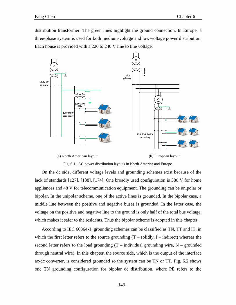
Fang Chen Chapter 6
-143-
distribution transformer. The green lines highlight the ground connection. In Europe, a
three-phase system is used for both medium-voltage and low-voltage power distribution.
Each house is provided with a 220 to 240 V line to line voltage.
12.47 kV
120/240 V secondary
primary
220, 230, 240 V secondary
120V 120V240V
11 kV
primary
(a) North American layout (b) European layout
Fig. 6.1. AC power distribution layouts in North America and Europe.
On the dc side, different voltage levels and grounding schemes exist because of the
lack of standards [127], [138], [174]. One broadly used configuration is 380 V for home
appliances and 48 V for telecommunication equipment. The grounding can be unipolar or
bipolar. In the unipolar scheme, one of the active lines is grounded. In the bipolar case, a
middle line between the positive and negative buses is grounded. In the latter case, the
voltage on the positive and negative line to the ground is only half of the total bus voltage,
which makes it safer to the residents. Thus the bipolar scheme is adopted in this chapter.
According to IEC 60364-1, grounding schemes can be classified as TN, TT and IT, in
which the first letter refers to the source grounding (T – solidly, I – indirect) whereas the
second letter refers to the load grounding (T – individual grounding wire, N – grounded
through neutral wire). In this chapter, the source side, which is the output of the interface
ac-dc converter, is considered grounded so the system can be TN or TT. Fig. 6.2 shows
one TN grounding configuration for bipolar dc distribution, where PE refers to the
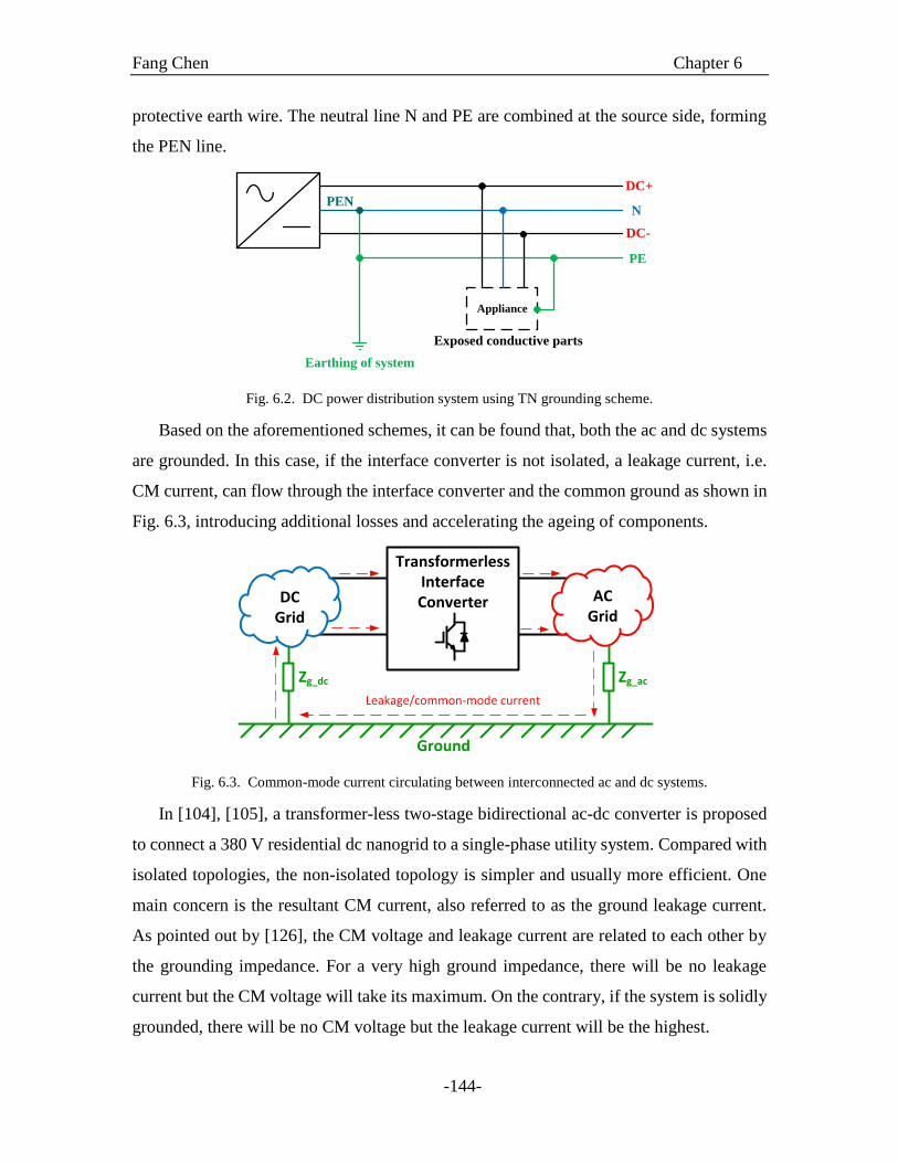
Fang Chen Chapter 6
-144-
protective earth wire. The neutral line N and PE are combined at the source side, forming
the PEN line.
DC+
DC-
N
PE
Appliance
PEN
Exposed conductive parts
Earthing of system
Fig. 6.2. DC power distribution system using TN grounding scheme.
Based on the aforementioned schemes, it can be found that, both the ac and dc systems
are grounded. In this case, if the interface converter is not isolated, a leakage current, i.e.
CM current, can flow through the interface converter and the common ground as shown in
Fig. 6.3, introducing additional losses and accelerating the ageing of components.
TransformerlessInterfaceConverter AC
GridDC
Grid
Zg_dc Zg_ac
Leakage/common-mode current
Ground
Fig. 6.3. Common-mode current circulating between interconnected ac and dc systems.
In [104], [105], a transformer-less two-stage bidirectional ac-dc converter is proposed
to connect a 380 V residential dc nanogrid to a single-phase utility system. Compared with
isolated topologies, the non-isolated topology is simpler and usually more efficient. One
main concern is the resultant CM current, also referred to as the ground leakage current.
As pointed out by [126], the CM voltage and leakage current are related to each other by
the grounding impedance. For a very high ground impedance, there will be no leakage
current but the CM voltage will take its maximum. On the contrary, if the system is solidly
grounded, there will be no CM voltage but the leakage current will be the highest.
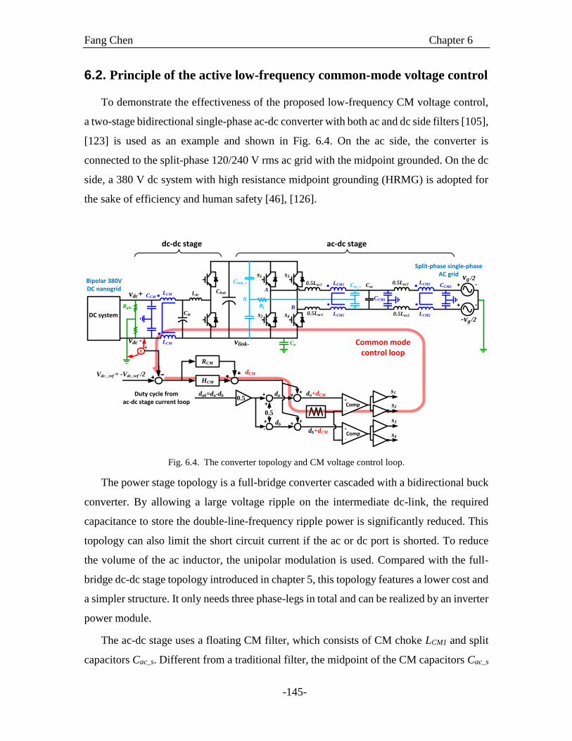
Fang Chen Chapter 6
-145-
6.2. Principle of the active low-frequency common-mode voltage control
To demonstrate the effectiveness of the proposed low-frequency CM voltage control,
a two-stage bidirectional single-phase ac-dc converter with both ac and dc side filters [105],
[123] is used as an example and shown in Fig. 6.4. On the ac side, the converter is
connected to the split-phase 120/240 V rms ac grid with the midpoint grounded. On the dc
side, a 380 V dc system with high resistance midpoint grounding (HRMG) is adopted for
the sake of efficiency and human safety [46], [126].
V
Vdc-_ref = -Vdc_ref /2HCM
RCM
dCM
+
-
+
-
+
+ +
-+
dab=da-db
0.5
Comp
Comp
+ da+dCM
+
+ da
db
db+dCM
0.5s1
s2
s3
s4
DC system
Ldcvdc+
0.5Lac2Cac
Cdc 0.5Lac1
Clink
vg0.5Lac1 LCM1
Clink_sCac_s
Cp
N
vlink-
A
B
CCM2
CCMLCM
Rgdc
0.5Lac2
vdc -
s1
s2
s3
s4
Bipolar 380V DC nanogrid
Split-phase single-phaseAC grid
LCM2
CCM1
Rf
Duty cycle from ac-dc stage current loop
ac-dc stagedc-dc stage
Common mode control loop
LCM
LCM1 LCM2
/2
-vg /2
+ -
+ -
Fig. 6.4. The converter topology and CM voltage control loop.
The power stage topology is a full-bridge converter cascaded with a bidirectional buck
converter. By allowing a large voltage ripple on the intermediate dc-link, the required
capacitance to store the double-line-frequency ripple power is significantly reduced. This
topology can also limit the short circuit current if the ac or dc port is shorted. To reduce
the volume of the ac inductor, the unipolar modulation is used. Compared with the full-
bridge dc-dc stage topology introduced in chapter 5, this topology features a lower cost and
a simpler structure. It only needs three phase-legs in total and can be realized by an inverter
power module.
The ac-dc stage uses a floating CM filter, which consists of CM choke LCM1 and split
capacitors Cac_s. Different from a traditional filter, the midpoint of the CM capacitors Cac_s
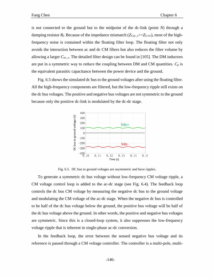
Fang Chen Chapter 6
-146-
is not connected to the ground but to the midpoint of the dc-link (point N) through a
damping resistor Rf. Because of the impedance mismatch (ZCac_s<<ZLCM2), most of the high-
frequency noise is contained within the floating filter loop. The floating filter not only
avoids the interaction between ac and dc CM filters but also reduces the filter volume by
allowing a larger Cac_s. The detailed filter design can be found in [105]. The DM inductors
are put in a symmetric way to reduce the coupling between DM and CM quantities. Cp is
the equivalent parasitic capacitance between the power device and the ground.
Fig. 6.5 shows the simulated dc bus to the ground voltages after using the floating filter.
All the high-frequency components are filtered, but the low-frequency ripple still exists on
the dc bus voltages. The positive and negative bus voltages are not symmetric to the ground
because only the positive dc-link is modulated by the dc-dc stage.
Vdc+
Vdc-
DC
bu
s to
gro
un
d v
olt
age
(V
)
Time (s)
Fig. 6.5. DC bus to ground voltages are asymmetric and have ripples.
To generate a symmetric dc bus voltage without low-frequency CM voltage ripple, a
CM voltage control loop is added to the ac-dc stage (see Fig. 6.4). The feedback loop
controls the dc bus CM voltage by measuring the negative dc bus to the ground voltage
and modulating the CM voltage of the ac-dc stage. When the negative dc bus is controlled
to be half of the dc bus voltage below the ground, the positive bus voltage will be half of
the dc bus voltage above the ground. In other words, the positive and negative bus voltages
are symmetric. Since this is a closed-loop system, it also suppresses the low-frequency
voltage ripple that is inherent in single-phase ac-dc conversion.
In the feedback loop, the error between the sensed negative bus voltage and its
reference is passed through a CM voltage controller. The controller is a multi-pole, multi-
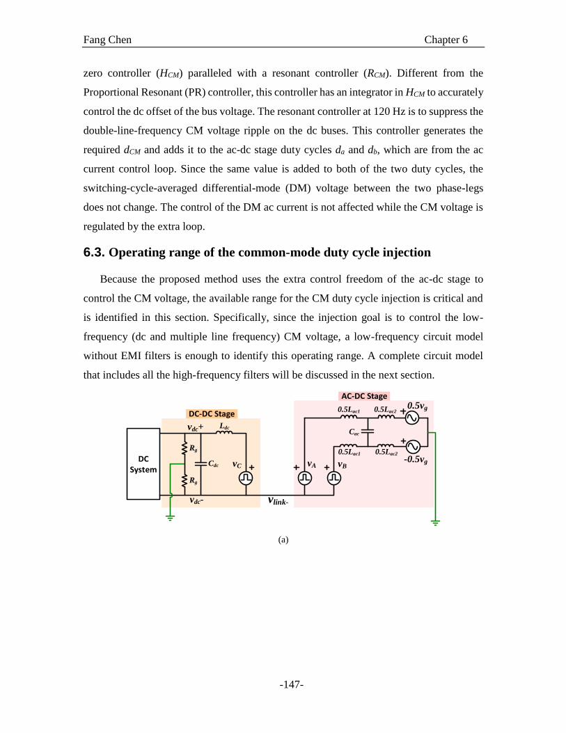
Fang Chen Chapter 6
-147-
zero controller (HCM) paralleled with a resonant controller (RCM). Different from the
Proportional Resonant (PR) controller, this controller has an integrator in HCM to accurately
control the dc offset of the bus voltage. The resonant controller at 120 Hz is to suppress the
double-line-frequency CM voltage ripple on the dc buses. This controller generates the
required dCM and adds it to the ac-dc stage duty cycles da and db, which are from the ac
current control loop. Since the same value is added to both of the two duty cycles, the
switching-cycle-averaged differential-mode (DM) voltage between the two phase-legs
does not change. The control of the DM ac current is not affected while the CM voltage is
regulated by the extra loop.
6.3. Operating range of the common-mode duty cycle injection
Because the proposed method uses the extra control freedom of the ac-dc stage to
control the CM voltage, the available range for the CM duty cycle injection is critical and
is identified in this section. Specifically, since the injection goal is to control the low-
frequency (dc and multiple line frequency) CM voltage, a low-frequency circuit model
without EMI filters is enough to identify this operating range. A complete circuit model
that includes all the high-frequency filters will be discussed in the next section.
0.5vg0.5Lac1
vlink-
0.5Lac2
Cac
DC System
Ldc
Cdc
Rg
Rg
vdc+
vdc-
vB
AC-DC Stage
DC-DC Stage
vC vA
0.5Lac1 0.5Lac2
-0.5vg
(a)
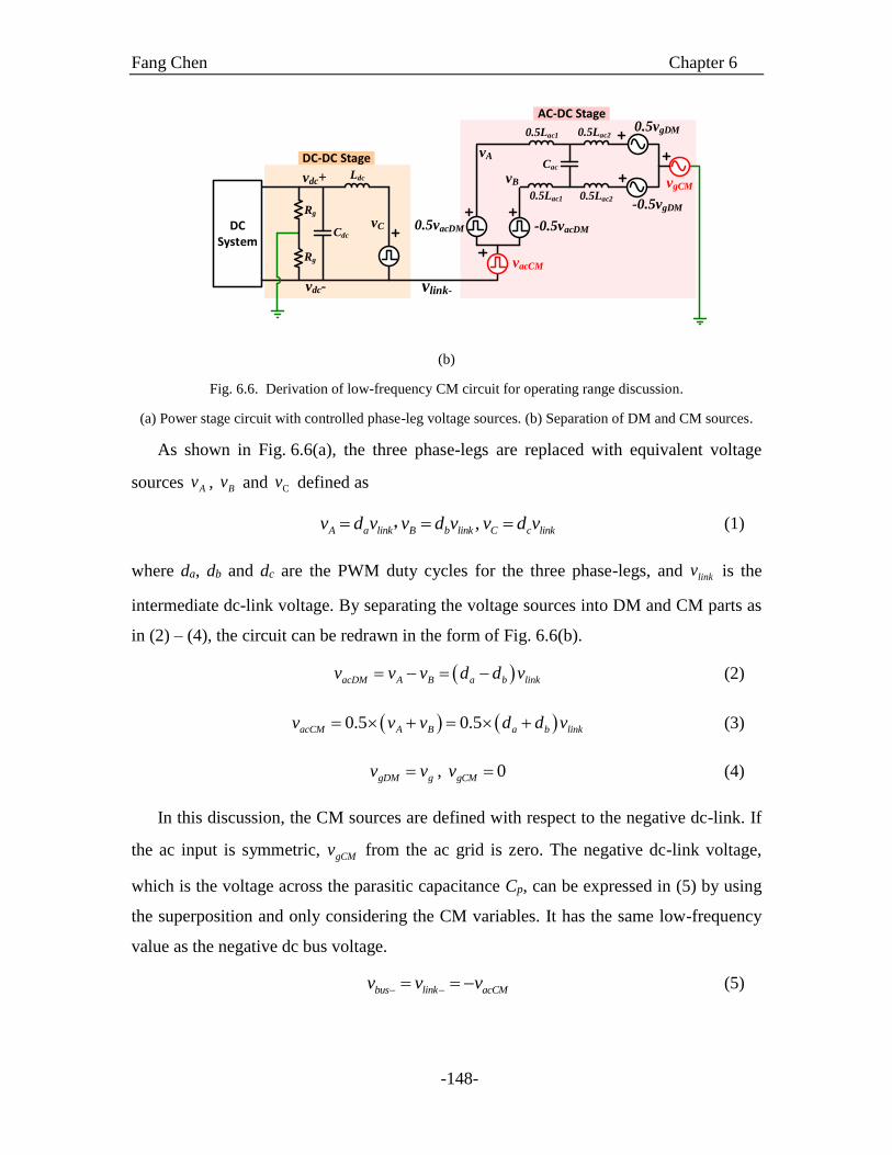
Fang Chen Chapter 6
-148-
0.5vgDM0.5Lac1
vlink-
0.5Lac2
Cac
DC System
Ldc
Cdc
Rg
Rg
vdc+
vdc-
vB
AC-DC Stage
DC-DC Stage
vC
vA
0.5Lac1 0.5Lac2
vacCM
0.5vacDM -0.5vacDM
-0.5vgDM
vgCM
(b)
Fig. 6.6. Derivation of low-frequency CM circuit for operating range discussion.
(a) Power stage circuit with controlled phase-leg voltage sources. (b) Separation of DM and CM sources.
As shown in Fig. 6.6(a), the three phase-legs are replaced with equivalent voltage
sources Av , Bv and Cv defined as
,A a link B b link C c linkv d v v d v v d v , (1)
where da, db and dc are the PWM duty cycles for the three phase-legs, and linkv is the
intermediate dc-link voltage. By separating the voltage sources into DM and CM parts as
in (2) – (4), the circuit can be redrawn in the form of Fig. 6.6(b).
acDM A B a b linkv v v d d v (2)
0.5 0.5acCM A B a b linkv v v d d v (3)
gDM gv v , 0gCMv (4)
In this discussion, the CM sources are defined with respect to the negative dc-link. If
the ac input is symmetric, gCMv from the ac grid is zero. The negative dc-link voltage,
which is the voltage across the parasitic capacitance Cp, can be expressed in (5) by using
the superposition and only considering the CM variables. It has the same low-frequency
value as the negative dc bus voltage.
bus link acCMv v v (5)
Fang Chen Chapter 6
-149-
Eq. (5) indicates that the negative dc bus voltage can be regulated by controlling the
ac-dc stage CM voltage, which is a function of the ac-dc stage duty cycles. It also shows
that the dc-dc stage does not influence the negative dc bus voltage.
Based on the control targets of the DM and CM voltage, we have the following two
expressions for the ac-dc stage
acDM gDMv v (6)
2
dcbus acCM
vv v (7)
Eq. (6) means the ac DM voltage roughly tracks the ac grid voltage to generate a
sinusoidal ac current. Eq. (7) on the other hand evinces that the CM control loop regulates
the negative dc bus voltage by controlling the CM voltage of the ac-dc stage. If the original
duty cycles from the ac current loop are defined as
0.5a DMd d (8)
0.5b DMd d (9)
After adding dCM to both da and db they can be rewritten as
0.5a DM CMd d d (10)
0.5b DM CMd d d (11)
Combining (2), (3), (6), (7), (10), (11) finally yields
1
2 2
g
DM a b
link
vd d d
v (12)
1
0.5 0.52 2
dcCM a b
link
vd d d
v (13)
Eq. (12) defines the required DM duty cycle to control the ac current, while (13) defines
the necessary CM duty cycle to control the dc bus voltages to be symmetric with respect
to ground. The duty cycle for each phase-leg is limited between 0 and 1, which is captured
by the following inequality:
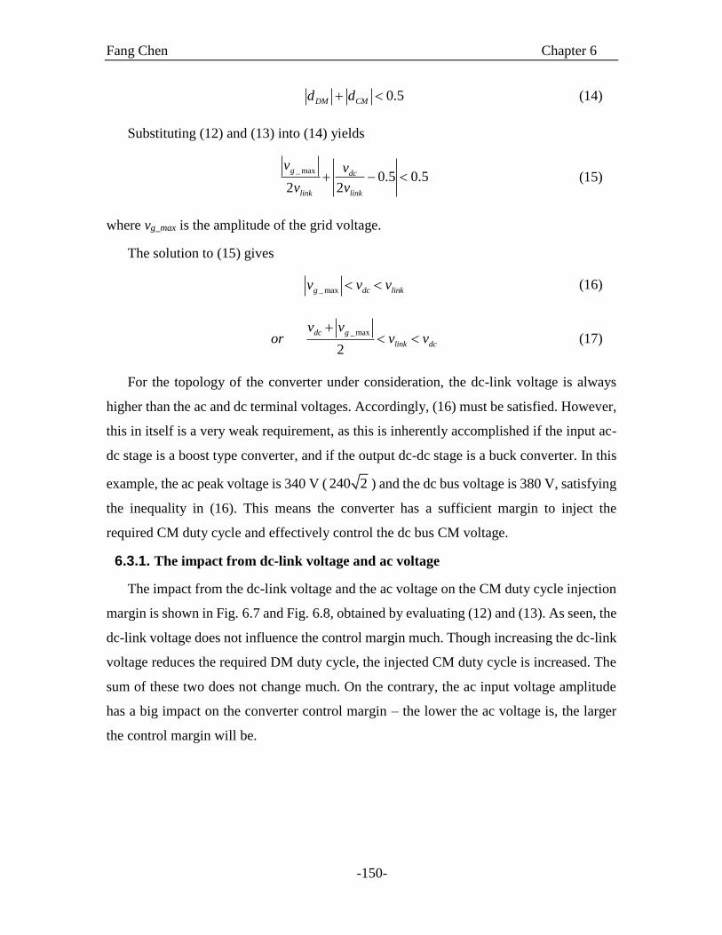
Fang Chen Chapter 6
-150-
0.5DM CMd d (14)
Substituting (12) and (13) into (14) yields
_ max
0.5 0.52 2
g dc
link link
v v
v v (15)
where vg_max is the amplitude of the grid voltage.
The solution to (15) gives
_ maxg dc linkv v v (16)
_ max
2
dc g
link dc
v vor v v
(17)
For the topology of the converter under consideration, the dc-link voltage is always
higher than the ac and dc terminal voltages. Accordingly, (16) must be satisfied. However,
this in itself is a very weak requirement, as this is inherently accomplished if the input ac-
dc stage is a boost type converter, and if the output dc-dc stage is a buck converter. In this
example, the ac peak voltage is 340 V ( 240 2 ) and the dc bus voltage is 380 V, satisfying
the inequality in (16). This means the converter has a sufficient margin to inject the
required CM duty cycle and effectively control the dc bus CM voltage.
6.3.1. The impact from dc-link voltage and ac voltage
The impact from the dc-link voltage and the ac voltage on the CM duty cycle injection
margin is shown in Fig. 6.7 and Fig. 6.8, obtained by evaluating (12) and (13). As seen, the
dc-link voltage does not influence the control margin much. Though increasing the dc-link
voltage reduces the required DM duty cycle, the injected CM duty cycle is increased. The
sum of these two does not change much. On the contrary, the ac input voltage amplitude
has a big impact on the converter control margin – the lower the ac voltage is, the larger
the control margin will be.
Fang Chen Chapter 6
-151-
400 500 600 700 800-0.3
-0.2
-0.1
0
0.1
0.2
0.3
0.4
0.5
Vlink
Du
ty c
yc
le
Ddm
Dcm
|Ddm|+|Dcm|
|Ddm|
|Dcm|
margin
Fig. 6.7. Impact from the dc-link voltage on the CM control margin.
50 100 150 200 250-0.2
-0.1
0
0.1
0.2
0.3
0.4
0.5
Vac
Du
ty c
yc
le
Ddm
Dcm
|Ddm|+|Dcm||Dcm|
|Ddm|
margin
Fig. 6.8. Impact from the ac voltage on the CM control margin.
Fig. 6.9 shows the time domain simulation with a 550 V dc-link voltage and a 240 V
split-phase ac input. After enabling the low-frequency CM voltage control, the dc bus is
controlled symmetric to the ground. Fig. 6.10 shows the duty cycles for the two phase-legs
of the ac-dc stage before and after enabling the CM control. As it is observed, a CM duty
cycle with some small ripple is injected.
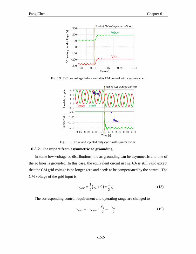
Fang Chen Chapter 6
-152-
Vdc+
Vdc-
Start of CM voltage control loop
DC
bu
s to
gro
un
d v
olt
age
(V)
Time (s)
Fig. 6.9. DC bus voltage before and after CM control with symmetric ac.
dutyA dutyB
Fin
al d
uty
cyc
le
Time (s)
dCM
dDM
Inje
cte
d d
CM
Start of CM voltage control
Fig. 6.10. Total and injected duty cycle with symmetric ac.
6.3.2. The impact from asymmetric ac grounding
In some low-voltage ac distributions, the ac grounding can be asymmetric and one of
the ac lines is grounded. In this case, the equivalent circuit in Fig. 6.6 is still valid except
that the CM grid voltage is no longer zero and needs to be compensated by the control. The
CM voltage of the grid input is
g
1 10
2 2CM g gv v v (18)
The corresponding control requirement and operating range are changed to
2 2
g dclink CMac
v vv v (19)
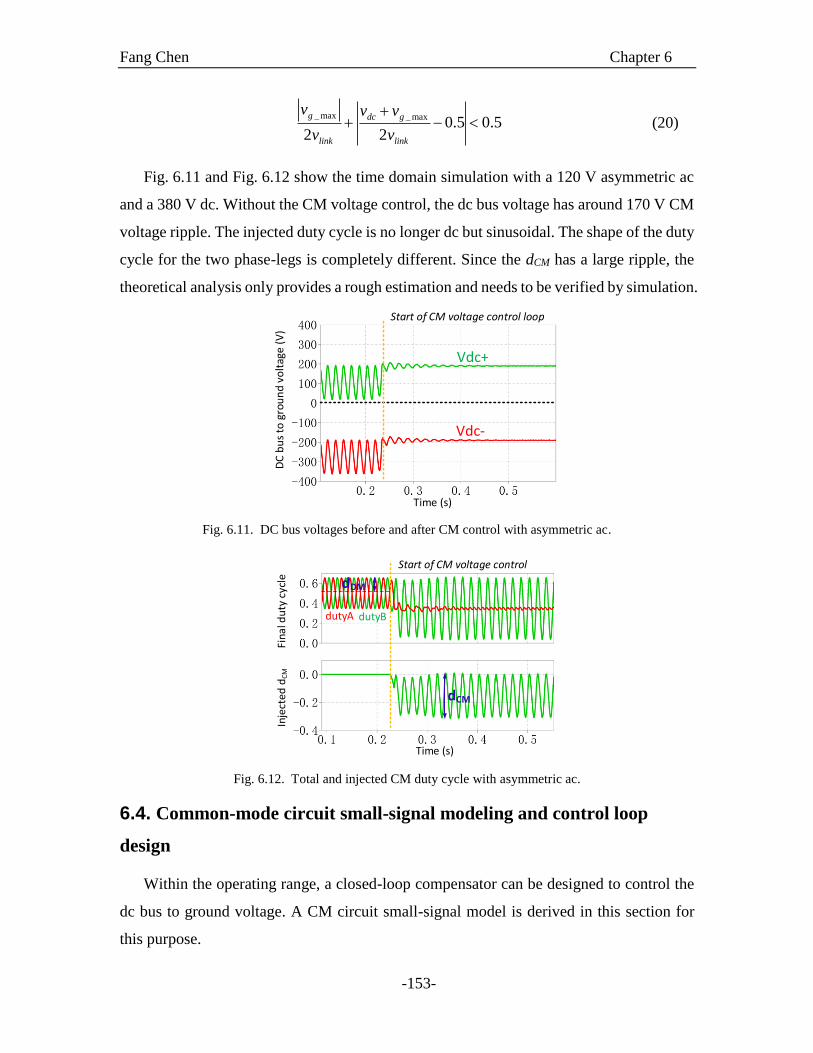
Fang Chen Chapter 6
-153-
_ max _ max
0.5 0.52 2
g dc g
link link
v v v
v v
(20)
Fig. 6.11 and Fig. 6.12 show the time domain simulation with a 120 V asymmetric ac
and a 380 V dc. Without the CM voltage control, the dc bus voltage has around 170 V CM
voltage ripple. The injected duty cycle is no longer dc but sinusoidal. The shape of the duty
cycle for the two phase-legs is completely different. Since the dCM has a large ripple, the
theoretical analysis only provides a rough estimation and needs to be verified by simulation.
Vdc+
Vdc-
Start of CM voltage control loop
Time (s)
DC
bu
s to
gro
un
d v
olt
age
(V)
Fig. 6.11. DC bus voltages before and after CM control with asymmetric ac.
dutyA dutyB
Time (s)
dCM
dDM
Inje
cte
d d
CM
Fin
al d
uty
cyc
le
Start of CM voltage control
Fig. 6.12. Total and injected CM duty cycle with asymmetric ac.
6.4. Common-mode circuit small-signal modeling and control loop
design
Within the operating range, a closed-loop compensator can be designed to control the
dc bus to ground voltage. A CM circuit small-signal model is derived in this section for
this purpose.

Fang Chen Chapter 6
-154-
2Clink_s
LCM1 LCM2
2Cac_s
vgCM
- +
LCM
0.5RgdcZCMbus 2CCM
Cp1 CCM2CCM1Cp2
Rf
LISN
RCM2RCM1RCM
LLISN
CLISN
RLISN
dcv acCM CM linkv d v
Z0 Z1 Z2
Zf
ZLISN
Zgdc
Fig. 6.13. Complete CM equivalent circuit with floating filter.
Based on the definition of the CM quantities, the complete CM equivalent circuit with
the floating filter is shown in Fig. 6.13. The physical meaning of each component can be
found in Fig. 6.4. A line stabilization network (LISN) is placed between the converter and
the ac grid to bypass the uncertainty of the line impedance from the ac side transformer
and utility. Cp1 and Cp2 are the parasitic capacitance from the semiconductor package to
ground. To simplify the derivation of small-signal transfer functions, equivalent
impedances are defined in Fig. 6.13 using red labels.
Defining
2 0total LISN gdcZ Z Z Z Z (21)
The transfer function from the controllable CM source to the negative dc bus voltage
can be expressed as
1
||
||
f total gdc
dc acCM
f total total
Z Z Zv v
Z Z Z Z
(22)
Combining (3) and (13), the transfer function from CM duty cycle to CM voltage
source can be expressed as
acCM CM linkv d v (23)
Then the transfer function from injected CM duty cycle to the negative bus voltage is
1
||
||
f total gdc
dc CM link
f total total
Z Z Zv d v
Z Z Z Z
(24)
To validate the model, online transfer function measurements are executed on the
hardware prototype with a digital processor. The switching frequency is 20 kHz. The
passive parameters are listed in Table 6.1. In the measurement, the DSP injects a series of
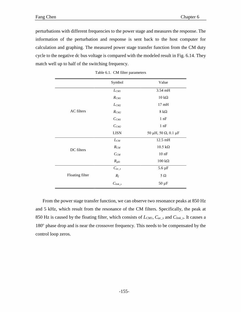
Fang Chen Chapter 6
-155-
perturbations with different frequencies to the power stage and measures the response. The
information of the perturbation and response is sent back to the host computer for
calculation and graphing. The measured power stage transfer function from the CM duty
cycle to the negative dc bus voltage is compared with the modeled result in Fig. 6.14. They
match well up to half of the switching frequency.
Table 6.1. CM filter parameters
Symbol Value
AC filters
LCM1 3.54 mH
RCM1 10 kΩ
LCM2 17 mH
RCM2 8 kΩ
CCM1 1 nF
CCM2 1 nF
LISN 50 µH, 50 Ω, 0.1 µF
DC filters
LCM 12.5 mH
RCM 10.5 kΩ
CCM 10 nF
Rgdc 100 kΩ
Floating filter
Cac_s 5.6 µF
Rf 5 Ω
Clink_s 50 µF
From the power stage transfer function, we can observe two resonance peaks at 850 Hz
and 5 kHz, which result from the resonance of the CM filters. Specifically, the peak at
850 Hz is caused by the floating filter, which consists of LCM1, Cac_s and Clink_s. It causes a
180 phase drop and is near the crossover frequency. This needs to be compensated by the
control loop zeros.
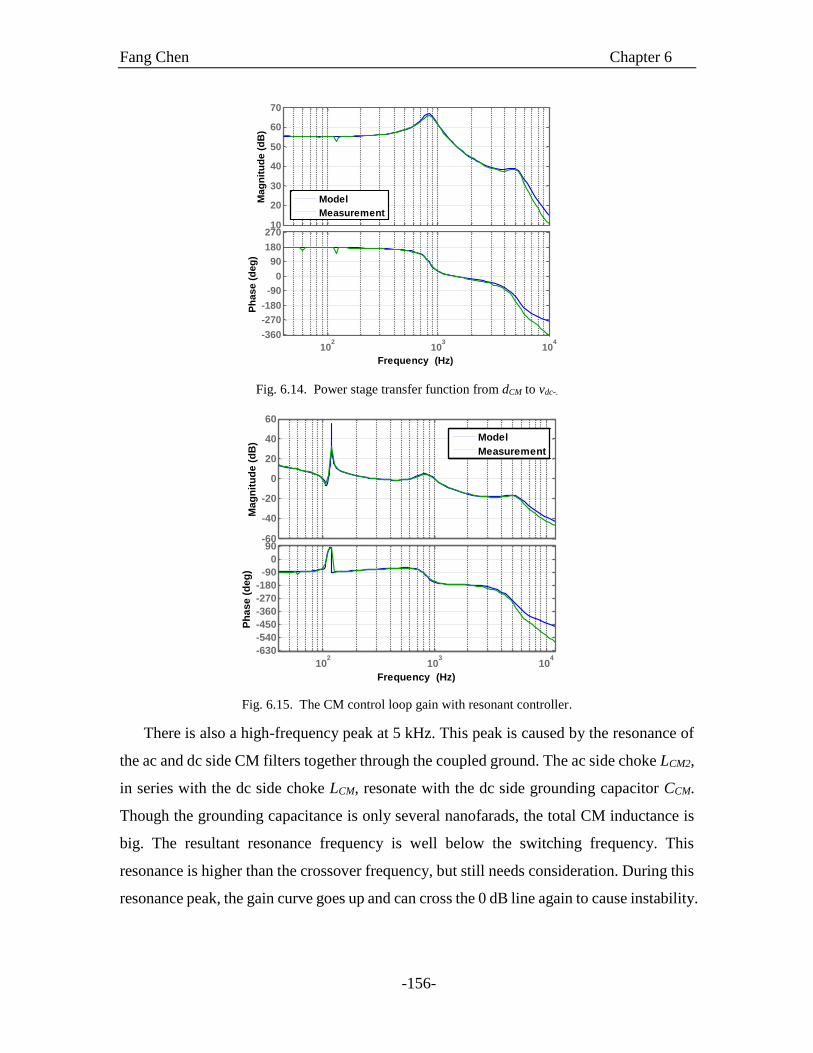
Fang Chen Chapter 6
-156-
Fig. 6.14. Power stage transfer function from dCM to vdc-.
Fig. 6.15. The CM control loop gain with resonant controller.
There is also a high-frequency peak at 5 kHz. This peak is caused by the resonance of
the ac and dc side CM filters together through the coupled ground. The ac side choke LCM2,
in series with the dc side choke LCM, resonate with the dc side grounding capacitor CCM.
Though the grounding capacitance is only several nanofarads, the total CM inductance is
big. The resultant resonance frequency is well below the switching frequency. This
resonance is higher than the crossover frequency, but still needs consideration. During this
resonance peak, the gain curve goes up and can cross the 0 dB line again to cause instability.
10
20
30
40
50
60
70
Mag
nit
ud
e (
dB
)
102
103
104
-360
-270
-180
-90
0
90
180
270
Ph
ase (
deg
)
Frequency (Hz)
Model
Measurement
-60
-40
-20
0
20
40
60
Mag
nit
ud
e (
dB
)
102
103
104
-630
-540
-450
-360
-270
-180
-90
0
90
Ph
ase (
deg
)
Frequency (Hz)
Model
Measurement
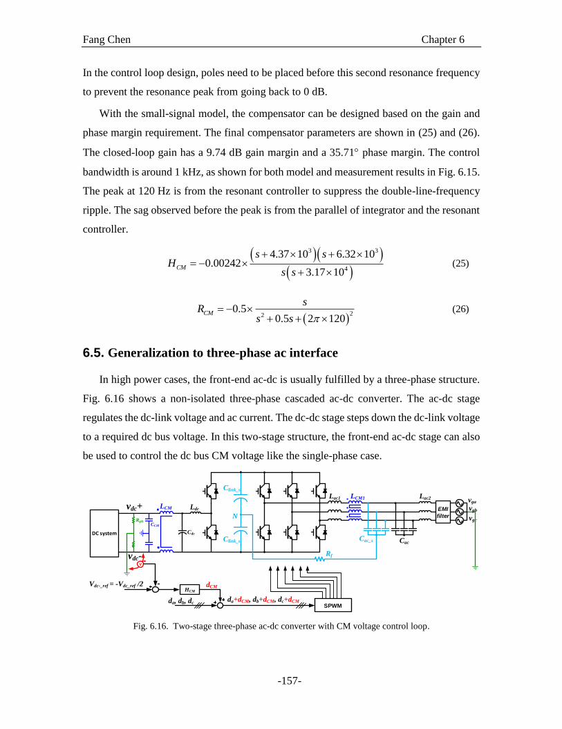
Fang Chen Chapter 6
-157-
In the control loop design, poles need to be placed before this second resonance frequency
to prevent the resonance peak from going back to 0 dB.
With the small-signal model, the compensator can be designed based on the gain and
phase margin requirement. The final compensator parameters are shown in (25) and (26).
The closed-loop gain has a 9.74 dB gain margin and a 35.71 phase margin. The control
bandwidth is around 1 kHz, as shown for both model and measurement results in Fig. 6.15.
The peak at 120 Hz is from the resonant controller to suppress the double-line-frequency
ripple. The sag observed before the peak is from the parallel of integrator and the resonant
controller.
3 3
4
4.37 10 6.32 100.00242
3.17 10CM
s sH
s s
(25)
220.5
0.5 2 120CM
sR
s s
(26)
6.5. Generalization to three-phase ac interface
In high power cases, the front-end ac-dc is usually fulfilled by a three-phase structure.
Fig. 6.16 shows a non-isolated three-phase cascaded ac-dc converter. The ac-dc stage
regulates the dc-link voltage and ac current. The dc-dc stage steps down the dc-link voltage
to a required dc bus voltage. In this two-stage structure, the front-end ac-dc stage can also
be used to control the dc bus CM voltage like the single-phase case.
N
LCM1Lac1
Cac_s
Clink_s
Clink_s
Lac2
EMI
filter
vga
vgb
vgc
Cac
Rf
DC system
Ldcvdc+
Cdc
CCM
LCM
Rgdc
vdc-V
Vdc-_ref = -Vdc_ref /2HCM
dCM
da, db, dcSPWM
da+dCM, db+dCM, dc+dCM
Fig. 6.16. Two-stage three-phase ac-dc converter with CM voltage control loop.
Fang Chen Chapter 6
-158-
The modulation scheme for three-phase converters can be either carrier-based SPWM
or space vector modulation (SVM). The benefits of SVM are better dc-link voltage
utilization and the possibility of reducing switching loss. However, it generates a low-
frequency CM voltage on the dc-link and dc bus, e.g. third order harmonic, which is not
good for the connection of the dc grid. On the other hand, SPWM shows a symmetric and
constant CM voltage.
Similar to the single-phase case, the control scheme for the three-phase front-end is
shown in Fig. 6.16. The CM voltage control loop generates the required dCM by comparing
the negative dc bus voltage with the reference. The injected duty cycle dCM is added to duty
cycles da, db and dc. In the three-phase case, there is no double-line-frequency voltage ripple
on the dc bus, so the resonant controller is unnecessary. The final dc bus voltage will be
symmetric to the ground.
6.6. Experimental results and impact on ac current
The proposed low-frequency CM voltage control method is verified using a 10 kW
single-phase bidirectional ac-dc converter. The experiment configuration is shown in Fig.
6.17. To accomplish the bidirectional power flow test, sources and loads are connected at
both sides of the ac-dc converter. On the ac side, the converter is connected to the ac grid
and some ac loads. On the dc side, a resistor bank is paralleled with electronic loads. The
electronic loads can be programmed to work in either constant resistive load (CRL) or
constant power load (CPL) mode. A current source is connected to the dc side to mimic
the output energy from renewable sources which usually work in maximum power point
tracking mode and do not regulate the bus voltage. When the injected current is smaller
than the local dc load consumption, the converter works in rectification mode. When the
renewable energy is greater than the local load, the extra energy is sent back to the grid,
and the converter works in regeneration mode. The converter topology and the CM filter
parameters are shown in Fig. 6.4 and Table 6.1.
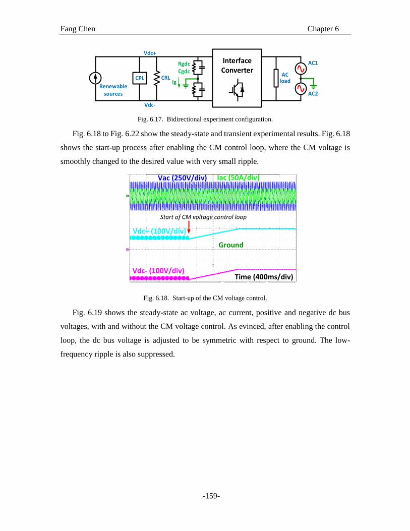
Fang Chen Chapter 6
-159-
InterfaceConverter
Vdc+
Vdc-
AC load
CRLCPLIg
RgdcCgdc
AC1
AC2Renewable
sources
Fig. 6.17. Bidirectional experiment configuration.
Fig. 6.18 to Fig. 6.22 show the steady-state and transient experimental results. Fig. 6.18
shows the start-up process after enabling the CM control loop, where the CM voltage is
smoothly changed to the desired value with very small ripple.
Vdc- (100V/div)
Vdc+ (100V/div)
Time (400ms/div)
Vac (250V/div) Iac (50A/div)
Start of CM voltage control loop
Ground
Fig. 6.18. Start-up of the CM voltage control.
Fig. 6.19 shows the steady-state ac voltage, ac current, positive and negative dc bus
voltages, with and without the CM voltage control. As evinced, after enabling the control
loop, the dc bus voltage is adjusted to be symmetric with respect to ground. The low-
frequency ripple is also suppressed.
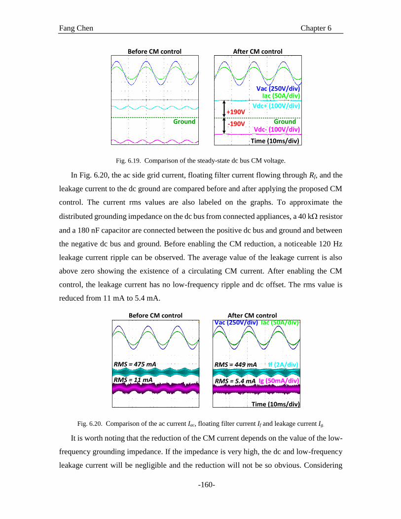
Fang Chen Chapter 6
-160-
Before CM control After CM control
+190V
-190V
Time (10ms/div)
Vdc- (100V/div)
Vdc+ (100V/div)
Vac (250V/div)Iac (50A/div)
Ground Ground
Fig. 6.19. Comparison of the steady-state dc bus CM voltage.
In Fig. 6.20, the ac side grid current, floating filter current flowing through Rf, and the
leakage current to the dc ground are compared before and after applying the proposed CM
control. The current rms values are also labeled on the graphs. To approximate the
distributed grounding impedance on the dc bus from connected appliances, a 40 k resistor
and a 180 nF capacitor are connected between the positive dc bus and ground and between
the negative dc bus and ground. Before enabling the CM reduction, a noticeable 120 Hz
leakage current ripple can be observed. The average value of the leakage current is also
above zero showing the existence of a circulating CM current. After enabling the CM
control, the leakage current has no low-frequency ripple and dc offset. The rms value is
reduced from 11 mA to 5.4 mA.
Before CM control After CM controlVac (250V/div) Iac (50A/div)
RMS = 11 mA
RMS = 475 mA
Time (10ms/div)
RMS = 5.4 mA
RMS = 449 mA
Ig (50mA/div)
If (2A/div)
Fig. 6.20. Comparison of the ac current Iac, floating filter current If and leakage current Ig.
It is worth noting that the reduction of the CM current depends on the value of the low-
frequency grounding impedance. If the impedance is very high, the dc and low-frequency
leakage current will be negligible and the reduction will not be so obvious. Considering
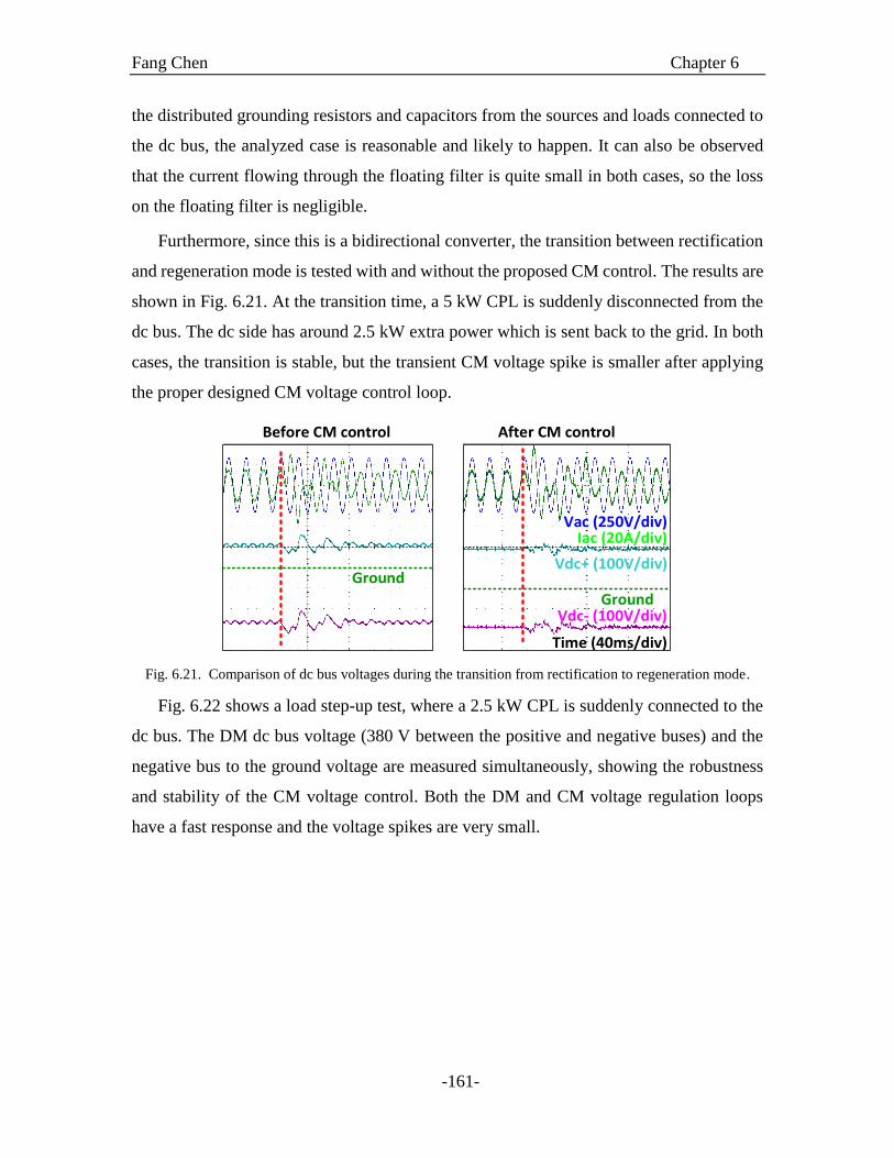
Fang Chen Chapter 6
-161-
the distributed grounding resistors and capacitors from the sources and loads connected to
the dc bus, the analyzed case is reasonable and likely to happen. It can also be observed
that the current flowing through the floating filter is quite small in both cases, so the loss
on the floating filter is negligible.
Furthermore, since this is a bidirectional converter, the transition between rectification
and regeneration mode is tested with and without the proposed CM control. The results are
shown in Fig. 6.21. At the transition time, a 5 kW CPL is suddenly disconnected from the
dc bus. The dc side has around 2.5 kW extra power which is sent back to the grid. In both
cases, the transition is stable, but the transient CM voltage spike is smaller after applying
the proper designed CM voltage control loop.
Vac (250V/div)Iac (20A/div)
Vdc- (100V/div)
Vdc+ (100V/div)
Time (40ms/div)
Before CM control After CM control
Ground
Ground
Fig. 6.21. Comparison of dc bus voltages during the transition from rectification to regeneration mode.
Fig. 6.22 shows a load step-up test, where a 2.5 kW CPL is suddenly connected to the
dc bus. The DM dc bus voltage (380 V between the positive and negative buses) and the
negative bus to the ground voltage are measured simultaneously, showing the robustness
and stability of the CM voltage control. Both the DM and CM voltage regulation loops
have a fast response and the voltage spikes are very small.
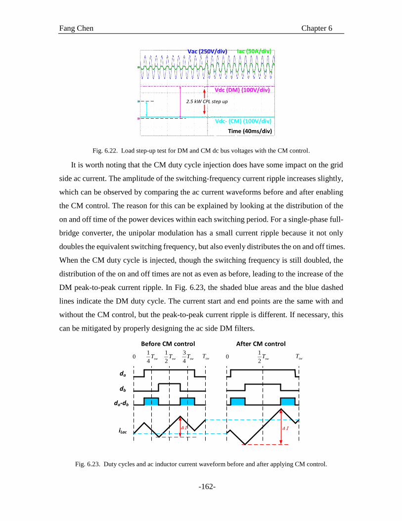
Fang Chen Chapter 6
-162-
Vac (250V/div) Iac (50A/div)
Vdc (DM) (100V/div)
Vdc- (CM) (100V/div)
Time (40ms/div)
2.5 kW CPL step up
Fig. 6.22. Load step-up test for DM and CM dc bus voltages with the CM control.
It is worth noting that the CM duty cycle injection does have some impact on the grid
side ac current. The amplitude of the switching-frequency current ripple increases slightly,
which can be observed by comparing the ac current waveforms before and after enabling
the CM control. The reason for this can be explained by looking at the distribution of the
on and off time of the power devices within each switching period. For a single-phase full-
bridge converter, the unipolar modulation has a small current ripple because it not only
doubles the equivalent switching frequency, but also evenly distributes the on and off times.
When the CM duty cycle is injected, though the switching frequency is still doubled, the
distribution of the on and off times are not as even as before, leading to the increase of the
DM peak-to-peak current ripple. In Fig. 6.23, the shaded blue areas and the blue dashed
lines indicate the DM duty cycle. The current start and end points are the same with and
without the CM control, but the peak-to-peak current ripple is different. If necessary, this
can be mitigated by properly designing the ac side DM filters.
da
db
da-db
iLacΔI ΔI
1
4swT
1
2swT
3
4swT swT0
1
2swT swT0
Before CM control After CM control
Fig. 6.23. Duty cycles and ac inductor current waveform before and after applying CM control.
Fang Chen Chapter 6
-163-
6.7. Conclusion
In this chapter, a transformer-less two-stage ac-dc converter is used as an example to
interconnect dc and ac power distribution systems, where the symmetry of the dc bus
voltage and ground leakage current are of big concern. A CM duty cycle injection method
is proposed to actively control the dc bus to ground voltage. As a result, the dc bus voltage
is rendered symmetric, and the low-frequency voltage ripple is fully suppressed. The
operating range of the proposed method is identified and shown to be feasible and practical;
an evaluation that also considers the impact of the ac and dc voltage levels as well as the
ac grounding schemes. To this end, a detailed CM circuit model is derived and validated,
and then used to design the closed-loop controller. Experimental results are presented to
verify the proposed control method under both steady-state and transient conditions, in the
presence of constant power loads, and under bidirectional power flow. The results obtained
also show how the ground leakage current is effectively reduced. Lastly, the control method
is generalized to three-phase ac-dc converters.

Fang Chen Chapter 7
-164-
Chapter 7. SUMMARY, CONCLUSIONS AND FUTURE WORK
7.1. Summary
1. A worst-case analysis is carried out for distributed dc systems to derive the
quantitative relation between the droop voltage range and the load sharing accuracy when
the line resistance cannot be neglected. DC system designers can use this relation to choose
a proper droop voltage range while guaranteeing the load sharing accuracy within a defined
range. Droop design guidelines are proposed for 380 V dc distribution systems.
2. A novel nonlinear droop method is proposed to improve the voltage regulation, load
sharing and system efficiency. By changing the droop resistance according to load
conditions, tighter voltage regulation under light load and better load sharing under heavy
load are achieved. These features also benefit the efficiency of dc systems. The output
impedance of droop-controlled power converters is also modeled and measured for system
stability analysis.
3. A secondary controller based on nearest-node communication is proposed to achieve
restored dc bus voltage, enhanced load sharing, and controllable tie-line power flow. With
the controller, the static bus voltage deviation from droop control is eliminated. The dc
system can achieve a higher efficiency under both light and heavy load conditions.
4. A high-efficiency bidirectional ac-dc converter is designed to connect the 380 V dc
and 240 V ac grids. A high-efficiency pluggable phase-leg structure is designed and tested.
Passive filters are also optimized based on the volt-second calculation. The resultant
converter can reach 97% efficiency for a wide load range. This is an increase of more than
7% over the previous design.
5. An active common-mode voltage control method is proposed to generate a
symmetric dc bus voltage for bipolar dc grids and reduce the leakage current. The common-
mode equivalent circuit modeling is presented and the control droop design is discussed.
The control method is applied to a two-stage ac-dc converter and tested under both rectifier
and inverter modes. Besides the generated symmetric dc bus voltage, the leakage current
is reduced by 50%.
7.2. Conclusions

Fang Chen Chapter 7
-165-
DC power distribution has simpler structure and is used in renewable energy systems
and microgrids. To achieve better performance, system level control is critical. Distributed
control is preferred due to the benefit of high reliability and flexibility. Droop control needs
no communication thus is suitable for the primary level control. But it suffers from the
impact of line resistance and measurement error. Worst-case analysis provides an
estimation of the lowest bus voltage and worst load sharing. Nonlinear droop and
secondary control with communication can improve the voltage regulation, load sharing,
and achieve higher system efficiency.
The interface converter between dc and ac grids processes the net energy of the dc
microgrid. Besides bidirectional power flow, the common-mode voltage and leakage
current control is important, especially for non-isolated topologies. Both passive filters and
control methods can be used to attenuate the common-mode quantities. The development
of wide-bandgap power devices enables the opportunity to achieve higher efficiency and
better manufacturability.
7.3. Future work
DC power distribution is an attractive and broad topic. Besides the work accomplished
in this dissertation, future research may concentrate on the following aspects:
1. EMI filter design for the interface converter. This dissertation mainly focuses on the
low-frequency common-mode attenuation. It is also important to comply with the EMI
standards required by the connected dc and ac systems. A special challenge in this
application is the interaction between the common-mode filters on both sides, since they
are coupled by the ground.
2. DC system stability with multiple sources and loads. With the development of dc
grids, different kinds of sources and loads will be connected to the bus. Determining how
to guarantee system stability and maintain system performance is an interesting and
important work.
3. DC circuit breakers and protection. As introduced in the first chapter, right now there
is still no satisfactory solution to interrupt the dc current. Mechanical switches respond
slowly while solid-state switches have large losses. As an indispensable part of the dc
distribution, research on the dc breaker is needed.

Fang Chen Chapter 7
-166-
4. Continuous improvement of the grid-interface converter. With the rapid
development of semiconductor techniques, the performance of wide-band-gap power
devices keeps improving. With better power devices, not only is the semiconductor loss
reduced, magnetic integration is also possible at higher switching frequency to achieve a
higher converter power density.
Fang Chen References
-167-
References
[1] Renewable Energy Policy Network for the 21st Century (REN21), “REN21 10 Year
Report,” [Online]. Available: http://www.ren21.net/spotlight/10-years-report/.
[2] S. Dasgupta, S. N. Mohan, S. K. Sahoo, and S. K. Panda, “A Plug and Play
Operational Approach for Implementation of an Autonomous-Micro-Grid System,”
IEEE Trans. Ind. Inform., vol. 8, no. 3, pp. 615–629, Aug. 2012.
[3] D. Boroyevich, I. Cvetković, D. Dong, R. Burgos, F. Wang, and F. Lee, “Future
electronic power distribution systems a contemplative view,” in Optimization of
Electrical and Electronic Equipment (OPTIM), 2010 12th International Conference
on, 2010, pp. 1369–1380.
[4] M. A. Maldonado and G. J. Korba, “Power management and distribution system for
a more-electric aircraft (MADMEL),” Aerosp. Electron. Syst. Mag. IEEE, vol. 14,
no. 12, pp. 3–8, 1999.
[5] H. Zhang, F. Mollet, C. Saudemont, and B. Robyns, “Experimental Validation of
Energy Storage System Management Strategies for a Local DC Distribution System
of More Electric Aircraft,” IEEE Trans. Ind. Electron., vol. 57, no. 12, pp. 3905–
3916, Dec. 2010.
[6] X. Roboam, B. Sareni, and A. Andrade, “More Electricity in the Air: Toward
Optimized Electrical Networks Embedded in More-Electrical Aircraft,” IEEE Ind.
Electron. Mag., vol. 6, no. 4, pp. 6–17, Dec. 2012.
[7] F. Wang, Z. Zhang, T. Ericsen, R. Raju, R. Burgos, and D. Boroyevich, “Advances
in Power Conversion and Drives for Shipboard Systems,” Proc. IEEE, vol. 103, no.
12, pp. 2285–2311, Dec. 2015.
[8] M. Farasat, A. Arabali, and A. M. Trzynadlowski, “Flexible-Voltage DC-Bus
Operation for Reduction of Switching Losses in All-Electric Ship Power Systems,”
IEEE Trans. Power Electron., vol. 29, no. 11, pp. 6151–6161, Nov. 2014.
[9] C.-L. Su, K.-L. Lin, and C.-J. Chen, “Power Flow and Generator-Converter Schemes
Studies in Ship MVDC Distribution Systems,” IEEE Trans. Ind. Appl., vol. 52, no.
1, pp. 50–59, Jan. 2016.
Fang Chen References
-168-
[10] M. Cupelli et al., “Power Flow Control and Network Stability in an All-Electric Ship,”
Proc. IEEE, vol. 103, no. 12, pp. 2355–2380, Dec. 2015.
[11] S. Jung, H. Lee, C. S. Song, J.-H. Han, W.-K. Han, and G. Jang, “Optimal Operation
Plan of the Online Electric Vehicle System Through Establishment of a DC
Distribution System,” IEEE Trans. Power Electron., vol. 28, no. 12, pp. 5878–5889,
Dec. 2013.
[12] M. Tariq et al., “Battery integration with more electric aircraft DC distribution
network using phase shifted high power bidirectional DC-DC converter,” in Power
and Energy Engineering Conference (APPEEC), 2015 IEEE PES Asia-Pacific, 2015,
pp. 1–5.
[13] E. B. Gietl, E. W. Gholdston, F. Cohen, B. A. Manners, and R. A. Delventhal, “The
architecture of the electric power system of the international space station and its
application as a platform for power technology development,” in Energy Conversion
Engineering Conference and Exhibit, 2000.(IECEC) 35th Intersociety, 2000, vol. 2,
pp. 855–864.
[14] S. Krauthamer, M. Gangal, and R. Das, “State of the art of DC components for
secondary power distribution of Space Station Freedom,” Power Electron. IEEE
Trans. On, vol. 6, no. 3, pp. 548–561, 1991.
[15] D. Salomonsson, L. Soder, and A. Sannino, “An Adaptive Control System for a DC
Microgrid for Data Centers,” IEEE Trans. Ind. Appl., vol. 44, no. 6, pp. 1910–1917,
2008.
[16] K. Hirose, “Dc power demonstrations in japan,” in Power Electronics and ECCE
Asia (ICPE & ECCE), 2011 IEEE 8th International Conference on, 2011, pp. 242–
247.
[17] A. Pratt, P. Kumar, and T. V. Aldridge, “Evaluation of 400V DC distribution in telco
and data centers to improve energy efficiency,” in Telecommunications Energy
Conference, 2007. INEC 2007. 29th International, 2007, pp. 32–39.
[18] P. Torcellini, S. Pless, M. Deru, and D. Crawley, “Zero energy buildings: a critical
look at the definition,” Natl. Renew. Energy Lab. Dep. Energy US, 2006.
[19] J. W. Baek, H. S. Kim, M. H. Ryu, J. H. Kim, and T. J. Kim, “A study on the DC
distribution system for small scale residential buildings,” in Power Electronics and

Fang Chen References
-169-
ECCE Asia (ICPE-ECCE Asia), 2015 9th International Conference on, 2015, pp.
2527–2531.
[20] T. Samad, E. Koch, and P. Stluka, “Automated Demand Response for Smart
Buildings and Microgrids: The State of the Practice and Research Challenges,” Proc.
IEEE, vol. 104, no. 4, pp. 726–744, Apr. 2016.
[21] H. Kakigano, Y. Miura, and T. Ise, “Configuration and control of a DC microgrid
for residential houses,” in Transmission & Distribution Conference & Exposition:
Asia and Pacific, 2009, 2009, pp. 1–4.
[22] B. T. Patterson, “DC, Come Home: DC Microgrids and the Birth of the ‘Enernet,’”
IEEE Power Energy Mag., vol. 10, no. 6, pp. 60–69, Nov. 2012.
[23] D. J. Becker and B. J. Sonnenberg, “DC microgrids in buildings and data centers,”
in Telecommunications Energy Conference (INEC), 2011 IEEE 33rd
International, 2011, pp. 1–7.
[24] V. Vossos, K. Garbesi, and H. Shen, “Energy savings from direct-DC in U.S.
residential buildings,” Energy Build., vol. 68, pp. 223–231, Jan. 2014.
[25] H. Kakigano, Y. Miura, T. Ise, T. Momose, and H. Hayakawa, “Fundamental
characteristics of DC microgrid for residential houses with cogeneration system in
each house,” in Power and Energy Society General Meeting-Conversion and
Delivery of Electrical Energy in the 21st Century, 2008 IEEE, 2008, pp. 1–8.
[26] E. Rodriguez Diaz, X. Su, M. Savaghebi, J. C. Vasquez, M. Han, and J. M. Guerrero,
“Intelligent DC Microgrid living Laboratories-A Chinese-Danish cooperation
project,” in DC Microgrids (ICDCM), 2015 IEEE First International Conference on,
2015, pp. 365–370.
[27] H. Kakigano, M. Nomura, and T. Ise, “Loss evaluation of DC distribution for
residential houses compared with AC system,” in Power Electronics Conference
(IPEC), 2010 International, 2010, pp. 480–486.
[28] W. Li, X. Mou, Y. Zhou, and C. Marnay, “On voltage standards for DC home
microgrids energized by distributed sources,” in Power Electronics and Motion
Control Conference (IPEMC), 2012 7th International, 2012, vol. 3, pp. 2282–2286.
Fang Chen References
-170-
[29] C. Marnay, G. Venkataramanan, M. Stadler, A. S. Siddiqui, R. Firestone, and B.
Chandran, “Optimal Technology Selection and Operation of Commercial-Building
Microgrids,” IEEE Trans. Power Syst., vol. 23, no. 3, pp. 975–982, Aug. 2008.
[30] T. Kaipia et al., “Field test environment for LVDC distribution — Implementation
experiences,” in CIRED 2012 Workshop: Integration of Renewables into the
Distribution Grid, 2012, pp. 1–4.
[31] A. Lana, A. Pinomaa, P. Nuutinen, T. Kaipia, and J. Partanen, “Control and
monitoring solution for the LVDC power distribution network research site,” in 2015
IEEE First International Conference on DC Microgrids (ICDCM), 2015, pp. 7–12.
[32] T. Dragicevic, H. Pandzic, D. Skrlec, I. Kuzle, J. M. Guerrero, and D. S. Kirschen,
“Capacity Optimization of Renewable Energy Sources and Battery Storage in an
Autonomous Telecommunication Facility,” IEEE Trans. Sustain. Energy, vol. 5, no.
4, pp. 1367–1378, Oct. 2014.
[33] S. Vazquez, S. M. Lukic, E. Galvan, L. G. Franquelo, and J. M. Carrasco, “Energy
Storage Systems for Transport and Grid Applications,” IEEE Trans. Ind. Electron.,
vol. 57, no. 12, pp. 3881–3895, Dec. 2010.
[34] D. Van Hertem and M. Ghandhari, “Multi-terminal VSC HVDC for the European
supergrid: Obstacles,” Renew. Sustain. Energy Rev., vol. 14, no. 9, pp. 3156–3163,
Dec. 2010.
[35] I. Cvetkovic et al., “A testbed for experimental validation of a low-voltage DC
nanogrid for buildings,” in Power Electronics and Motion Control Conference
(EPE/PEMC), 2012 15th International, 2012, p. LS7c–5.
[36] D. Boroyevich, R. Burgos, L. Arnedo, and F. Wang, “Synthesis and integration of
future electronic power distribution systems,” in Power Conversion Conference-
Nagoya, 2007. PCC’07, 2007, p. K–1.
[37] A. Q. Huang, M. L. Crow, G. T. Heydt, J. P. Zheng, and S. J. Dale, “The Future
Renewable Electric Energy Delivery and Management (FREEDM) System: The
Energy Internet,” Proc. IEEE, vol. 99, no. 1, pp. 133–148, Jan. 2011.
[38] A. Q. Huang, L. Wang, Q. Tian, Q. Zhu, D. Chen, and W. Yu, “Medium voltage
solid state transformers based on 15 kV SiC MOSFET and JBS diode,” in IECON
Fang Chen References
-171-
2016 - 42nd Annual Conference of the IEEE Industrial Electronics Society, 2016,
pp. 6996–7002.
[39] L. Wang, Q. Zhu, W. Yu, and A. Q. Huang, “A Medium-Voltage Medium-
Frequency Isolated DC–DC Converter Based on 15-kV SiC MOSFETs,” IEEE J.
Emerg. Sel. Top. Power Electron., vol. 5, no. 1, pp. 100–109, Mar. 2017.
[40] L. Wang, Q. Zhu, W. Yu, and A. Q. Huang, “A medium voltage bidirectional DC-
DC converter combining resonant and dual active bridge converters,” in 2015 IEEE
Applied Power Electronics Conference and Exposition (APEC), 2015, pp. 1104–
1111.
[41] L. Wang, Q. Zhu, W. Yu, and A. Q. Huang, “A study of dynamic high voltage output
charge measurement for 15 kV SiC MOSFET,” in 2016 IEEE Energy Conversion
Congress and Exposition (ECCE), 2016, pp. 1–7.
[42] H. Nikkhajoei and R. H. Lasseter, “Distributed Generation Interface to the CERTS
Microgrid,” IEEE Trans. Power Deliv., vol. 24, no. 3, pp. 1598–1608, Jul. 2009.
[43] L. Meng et al., “Flexible System Integration and Advanced Hierarchical Control
Architectures in the Microgrid Research Laboratory of Aalborg University,” IEEE
Trans. Ind. Appl., pp. 1–1, 2015.
[44] J. M. Guerrero, J. C. Vasquez, J. Matas, L. G. de Vicuna, and M. Castilla,
“Hierarchical Control of Droop-Controlled AC and DC Microgrids-A General
Approach Toward Standardization,” IEEE Trans. Ind. Electron., vol. 58, no. 1, pp.
158–172, Jan. 2011.
[45] M.-H. Ryu, H.-S. Kim, J.-W. Baek, H.-G. Kim, and J.-H. Jung, “Effective Test Bed
of 380-V DC Distribution System Using Isolated Power Converters,” IEEE Trans.
Ind. Electron., vol. 62, no. 7, pp. 4525–4536, Jul. 2015.
[46] H. Kakigano, Y. Miura, and T. Ise, “Low-Voltage Bipolar-Type DC Microgrid for
Super High Quality Distribution,” IEEE Trans. Power Electron., vol. 25, no. 12, pp.
3066–3075, Dec. 2010.
[47] B. K. Johnson and R. Lasseter, “An industrial power distribution system featuring
UPS properties,” in Power Electronics Specialists Conference, 1993. PESC’93
Record., 24th Annual IEEE, 1993, pp. 759–765.
Fang Chen References
-172-
[48] R. H. Lasseter, “Microgrids,” in Power Engineering Society Winter Meeting, 2002.
IEEE, 2002, vol. 1, pp. 305–308.
[49] Y. Ito, Y. Zhongqing, and H. Akagi, “DC microgrid based distribution power
generation system,” in Power Electronics and Motion Control Conference, 2004.
IPEMC 2004. The 4th International, 2004, vol. 3, pp. 1740–1745.
[50] M. Brenna, E. Tironi, and G. Ubezio, “Proposal of a local dc distribution network
with distributed energy resources,” in Harmonics and Quality of Power, 2004. 11th
International Conference on, 2004, pp. 397–402.
[51] M. H. Nehrir et al., “A Review of Hybrid Renewable/Alternative Energy Systems
for Electric Power Generation: Configurations, Control, and Applications,” IEEE
Trans. Sustain. Energy, vol. 2, no. 4, pp. 392–403, Oct. 2011.
[52] K. Miettinen, Nonlinear Multiobjective Optimization, vol. 12. Boston, MA: Springer
US, 1998.
[53] M. A. Abido, “Environmental/economic power dispatch using multiobjective
evolutionary algorithms,” IEEE Trans. Power Syst., vol. 18, no. 4, pp. 1529–1537,
Nov. 2003.
[54] Caisheng Wang and M. H. Nehrir, “Power Management of a Stand-Alone
Wind/Photovoltaic/Fuel Cell Energy System,” IEEE Trans. Energy Convers., vol.
23, no. 3, pp. 957–967, Sep. 2008.
[55] F. Valenciaga and P. F. Puleston, “Supervisor Control for a Stand-Alone Hybrid
Generation System Using Wind and Photovoltaic Energy,” IEEE Trans. Energy
Convers., vol. 20, no. 2, pp. 398–405, Jun. 2005.
[56] Y. Panov, J. Rajagopalan, and F. C. Lee, “Analysis and design of N paralleled DC-
DC converters with master-slave current-sharing control,” in Applied Power
Electronics Conference and Exposition, 1997. APEC’97 Conference Proceedings
1997., Twelfth Annual, 1997, vol. 1, pp. 436–442.
[57] M. E. Torres-Hernandez and M. Velez-Reyes, “Hierarchical control of Hybrid
Power Systems,” in Power Electronics Congress, 2008. CIEP 2008. 11th IEEE
International, 2008, pp. 169–176.
Fang Chen References
-173-
[58] K. De Brabandere, K. Vanthournout, J. Driesen, G. Deconinck, and R. Belmans,
“Control of microgrids,” in Power Engineering Society General Meeting, 2007.
IEEE, 2007, pp. 1–7.
[59] Liang Che and M. Shahidehpour, “DC Microgrids: Economic Operation and
Enhancement of Resilience by Hierarchical Control,” IEEE Trans. Smart Grid, vol.
5, no. 5, pp. 2517–2526, Sep. 2014.
[60] Q. Shafiee, T. Dragicevic, J. C. Vasquez, and J. M. Guerrero, “Hierarchical control
for multiple dc-microgrids clusters,” Energy Convers. IEEE Trans. On, vol. 29, no.
4, pp. 922–933, 2014.
[61] T. Dragicevic, J. M. Guerrero, J. C. Vasquez, and D. Skrlec, “Supervisory Control
of an Adaptive-Droop Regulated DC Microgrid With Battery Management
Capability,” IEEE Trans. Power Electron., vol. 29, no. 2, pp. 695–706, Feb. 2014.
[62] C. Jin, P. Wang, J. Xiao, Y. Tang, and F. H. Choo, “Implementation of Hierarchical
Control in DC Microgrids,” IEEE Trans. Ind. Electron., vol. 61, no. 8, pp. 4032–
4042, Aug. 2014.
[63] X. Lu, J. M. Guerrero, K. Sun, J. C. Vasquez, R. Teodorescu, and L. Huang,
“Hierarchical Control of Parallel AC-DC Converter Interfaces for Hybrid
Microgrids,” IEEE Trans. Smart Grid, vol. 5, no. 2, pp. 683–692, Mar. 2014.
[64] J. Bryan, R. Duke, and S. Round, “Decentralized generator scheduling in a nanogrid
using DC bus signaling,” in Power Engineering Society General Meeting, 2004.
IEEE, 2004, pp. 977–982.
[65] J. Schonbergerschonberger, R. Duke, and S. D. Round, “DC-Bus Signaling: A
Distributed Control Strategy for a Hybrid Renewable Nanogrid,” IEEE Trans. Ind.
Electron., vol. 53, no. 5, pp. 1453–1460, Oct. 2006.
[66] Kai Sun, Li Zhang, Yan Xing, and J. M. Guerrero, “A Distributed Control Strategy
Based on DC Bus Signaling for Modular Photovoltaic Generation Systems With
Battery Energy Storage,” IEEE Trans. Power Electron., vol. 26, no. 10, pp. 3032–
3045, Oct. 2011.
[67] L. Zhang, T. Wu, Y. Xing, K. Sun, and J. M. Gurrero, “Power control of DC
microgrid using DC bus signaling,” in Applied Power Electronics Conference and
Exposition (APEC), 2011 Twenty-Sixth Annual IEEE, 2011, pp. 1926–1932.

Fang Chen References
-174-
[68] Y. Gu, X. Xiang, W. Li, and X. He, “Mode-Adaptive Decentralized Control for
Renewable DC Microgrid With Enhanced Reliability and Flexibility,” IEEE Trans.
Power Electron., vol. 29, no. 9, pp. 5072–5080, Sep. 2014.
[69] D. J. Perreault, R. L. Selders, and J. G. Kassakian, “Frequency-based current-sharing
techniques for paralleled power converters,” IEEE Trans. Power Electron., vol. 13,
no. 4, pp. 626–634, Jul. 1998.
[70] W. Stefanutti, S. Saggini, P. Mattavelli, and M. Ghioni, “Power Line
Communication in Digitally Controlled DC-DC Converters Using Switching
Frequency Modulation,” IEEE Trans. Ind. Electron., vol. 55, no. 4, pp. 1509–1518,
Apr. 2008.
[71] S. Anand, B. G. Fernandes, and J. Guerrero, “Distributed Control to Ensure
Proportional Load Sharing and Improve Voltage Regulation in Low-Voltage DC
Microgrids,” IEEE Trans. Power Electron., vol. 28, no. 4, pp. 1900–1913, Apr. 2013.
[72] X. Lu, J. M. Guerrero, K. Sun, and J. C. Vasquez, “An Improved Droop Control
Method for DC Microgrids Based on Low Bandwidth Communication With DC Bus
Voltage Restoration and Enhanced Current Sharing Accuracy,” IEEE Trans. Power
Electron., vol. 29, no. 4, pp. 1800–1812, Apr. 2014.
[73] P.-H. Huang, P.-C. Liu, W. Xiao, and M. S. El Moursi, “A Novel Droop-Based
Average Voltage Sharing Control Strategy for DC Microgrids,” IEEE Trans. Smart
Grid, vol. 6, no. 3, pp. 1096–1106, May 2015.
[74] P. Wang, X. Lu, X. Yang, W. Wang, and D. Xu, “An Improved Distributed
Secondary Control Method for DC Microgrids With Enhanced Dynamic Current
Sharing Performance,” IEEE Trans. Power Electron., vol. 31, no. 9, pp. 6658–6673,
Sep. 2016.
[75] H. M. Kelash, H. M. Faheem, and M. Amoon, “It takes a multiagent system to
manage distributed systems,” IEEE Potentials, vol. 26, no. 2, pp. 39–45, Mar. 2007.
[76] A. L. Dimeas and N. D. Hatziargyriou, “Operation of a Multiagent System for
Microgrid Control,” IEEE Trans. Power Syst., vol. 20, no. 3, pp. 1447–1455, Aug.
2005.

Fang Chen References
-175-
[77] K. Huang, D. A. Cartes, and S. K. Srivastava, “A Multiagent-Based Algorithm for
Ring-Structured Shipboard Power System Reconfiguration,” IEEE Trans. Syst. Man
Cybern. Part C Appl. Rev., vol. 37, no. 5, pp. 1016–1021, Sep. 2007.
[78] V. Nasirian, A. Davoudi, F. L. Lewis, and J. M. Guerrero, “Distributed Adaptive
Droop Control for DC Distribution Systems,” IEEE Trans. Energy Convers., vol. 29,
no. 4, pp. 944–956, Dec. 2014.
[79] F. Guo, C. Wen, J. Mao, and Y.-D. Song, “Distributed Secondary Voltage and
Frequency Restoration Control of Droop-Controlled Inverter-Based Microgrids,”
IEEE Trans. Ind. Electron., vol. 62, no. 7, pp. 4355–4364, Jul. 2015.
[80] L. Meng, T. Dragicevic, J. Roldan-Perez, J. C. Vasquez, and J. M. Guerrero,
“Modeling and Sensitivity Study of Consensus Algorithm-Based Distributed
Hierarchical Control for DC Microgrids,” IEEE Trans. Smart Grid, vol. 7, no. 3, pp.
1504–1515, May 2016.
[81] V. Nasirian, Q. Shafiee, J. M. Guerrero, F. L. Lewis, and A. Davoudi, “Droop-Free
Distributed Control for AC Microgrids,” IEEE Trans. Power Electron., vol. 31, no.
2, pp. 1600–1617, Feb. 2016.
[82] R. Olfati-Saber and R. M. Murray, “Consensus problems in networks of agents with
switching topology and time-delays,” IEEE Trans. Autom. Control, vol. 49, no. 9,
pp. 1520–1533, Sep. 2004.
[83] R. Olfati-Saber, J. A. Fax, and R. M. Murray, “Consensus and Cooperation in
Networked Multi-Agent Systems,” Proc. IEEE, vol. 95, no. 1, pp. 215–233, Jan.
2007.
[84] T. Dragičević, X. Lu, J. C. Vasquez, and J. M. Guerrero, “DC Microgrids—Part I:
A Review of Control Strategies and Stabilization Techniques,” IEEE Trans. Power
Electron., vol. 31, no. 7, pp. 4876–4891, Jul. 2016.
[85] Y. Xue, L. Chang, S. B. Kjaer, J. Bordonau, and T. Shimizu, “Topologies of single-
phase inverters for small distributed power generators: an overview,” IEEE Trans.
Power Electron., vol. 19, no. 5, pp. 1305–1314, Sep. 2004.
[86] S. B. Kjaer, J. K. Pedersen, and F. Blaabjerg, “A review of single-phase grid-
connected inverters for photovoltaic modules,” IEEE Trans. Ind. Appl., vol. 41, no.
5, pp. 1292–1306, Sep. 2005.
Fang Chen References
-176-
[87] J. Walter and R. W. D. Doncker, “High-power galvanically isolated DC/DC
converter topology for future automobiles,” in Power Electronics Specialist
Conference, 2003. PESC ’03. 2003 IEEE 34th Annual, 2003, vol. 1, pp. 27–32 vol.1.
[88] K. Wang, F. C. Lee, and J. Lai, “Operation principles of bi-directional full-bridge
DC/DC converter with unified soft-switching scheme and soft-starting capability,”
in Fifteenth Annual IEEE Applied Power Electronics Conference and Exposition,
2000. APEC 2000, 2000, vol. 1, pp. 111–118 vol.1.
[89] R. Gonzalez, J. Lopez, P. Sanchis, and L. Marroyo, “Transformerless Inverter for
Single-Phase Photovoltaic Systems,” IEEE Trans. Power Electron., vol. 22, no. 2,
pp. 693–697, Mar. 2007.
[90] T. Kerekes, R. Teodorescu, M. Liserre, C. Klumpner, and M. Sumner, “Evaluation
of Three-Phase Transformerless Photovoltaic Inverter Topologies,” IEEE Trans.
Power Electron., vol. 24, no. 9, pp. 2202–2211, Sep. 2009.
[91] M. Chen, X. Lee, and Y. Tsutomu, “A novel soft-switching grid-connected PV
inverter and its implementation,” in 2011 IEEE Ninth International Conference on
Power Electronics and Drive Systems (PEDS), 2011, pp. 373–378.
[92] B. K. Bose and D. Kastha, “Electrolytic capacitor elimination in power electronic
system by high frequency active filter,” in , Conference Record of the 1991 IEEE
Industry Applications Society Annual Meeting, 1991, 1991, pp. 869–878 vol.1.
[93] P. N. Enjeti and W. Shireen, “A new technique to reject DC-link voltage ripple for
inverters operating on programmed PWM waveforms,” Power Electron. IEEE Trans.
On, vol. 7, no. 1, pp. 171–180, 1992.
[94] T. Shimizu, T. Fujita, G. Kimura, and J. Hirose, “A unity power factor PWM rectifier
with DC ripple compensation,” Ind. Electron. IEEE Trans. On, vol. 44, no. 4, pp.
447–455, 1997.
[95] P. T. Krein and R. S. Balog, “Cost-effective hundred-year life for single-phase
inverters and rectifiers in solar and LED lighting applications based on minimum
capacitance requirements and a ripple power port,” in Applied Power Electronics
Conference and Exposition, 2009. APEC 2009. Twenty-Fourth Annual IEEE, 2009,
pp. 620–625.
Fang Chen References
-177-
[96] R. Wang, F. Wang, R. Lai, P. Ning, R. Burgos, and D. Boroyevich, “Study of energy
storage capacitor reduction for single phase PWM rectifier,” in Applied Power
Electronics Conference and Exposition, 2009. APEC 2009. Twenty-Fourth Annual
IEEE, 2009, pp. 1177–1183.
[97] P. T. Krein, R. S. Balog, and M. Mirjafari, “Minimum Energy and Capacitance
Requirements for Single-Phase Inverters and Rectifiers Using a Ripple Port,” IEEE
Trans. Power Electron., vol. 27, no. 11, pp. 4690–4698, Nov. 2012.
[98] Ruxi Wang et al., “A High Power Density Single-Phase PWM Rectifier With Active
Ripple Energy Storage,” IEEE Trans. Power Electron., vol. 26, no. 5, pp. 1430–1443,
May 2011.
[99] Huai Wang, H. S.-H. Chung, and Wenchao Liu, “Use of a Series Voltage
Compensator for Reduction of the DC-Link Capacitance in a Capacitor-Supported
System,” IEEE Trans. Power Electron., vol. 29, no. 3, pp. 1163–1175, Mar. 2014.
[100]R. S. Balog and P. T. Krein, “Coupled-Inductor Filter: A Basic Filter Building Block,”
IEEE Trans. Power Electron., vol. 28, no. 1, pp. 537–546, Jan. 2013.
[101] H. Hu, S. Harb, N. Kutkut, I. Batarseh, and Z. J. Shen, “A Review of Power
Decoupling Techniques for Microinverters With Three Different Decoupling
Capacitor Locations in PV Systems,” IEEE Trans. Power Electron., vol. 28, no. 6,
pp. 2711–2726, Jun. 2013.
[102] Y. Tang, F. Blaabjerg, P. C. Loh, C. Jin, and P. Wang, “Decoupling of Fluctuating
Power in Single-Phase Systems Through a Symmetrical Half-Bridge Circuit,” IEEE
Trans. Power Electron., vol. 30, no. 4, pp. 1855–1865, Apr. 2015.
[103] S. Li, G.-R. Zhu, S.-C. Tan, and S. Y. R. Hui, “Direct AC/DC Rectifier With
Mitigated Low-Frequency Ripple Through Inductor-Current Waveform Control,”
IEEE Trans. Power Electron., vol. 30, no. 8, pp. 4336–4348, Aug. 2015.
[104] D. Dong, I. Cvetkovic, D. Boroyevich, W. Zhang, R. Wang, and P. Mattavelli, “Grid-
Interface Bidirectional Converter for Residential DC Distribution Systems—Part
One: High-Density Two-Stage Topology,” IEEE Trans. Power Electron., vol. 28,
no. 4, pp. 1655–1666, Apr. 2013.
[105] D. Dong, F. Luo, X. Zhang, D. Boroyevich, and P. Mattavelli, “Grid-Interface
Bidirectional Converter for Residential DC Distribution Systems—Part 2: AC and
Fang Chen References
-178-
DC Interface Design With Passive Components Minimization,” IEEE Trans. Power
Electron., vol. 28, no. 4, pp. 1667–1679, Apr. 2013.
[106] G. Meyer-Brotz and A. Kley, “The Common-Mode Rejection of Transistor
Differential Amplifiers,” IEEE Trans. Circuit Theory, vol. 13, no. 2, pp. 171–175,
Jun. 1966.
[107] D. E. Bockelman and W. R. Eisenstadt, “Combined differential and common-mode
scattering parameters: theory and simulation,” IEEE Trans. Microw. Theory Tech.,
vol. 43, no. 7, pp. 1530–1539, Jul. 1995.
[108] R. Gonzalez, E. Gubia, J. Lopez, and L. Marroyo, “Transformerless Single-Phase
Multilevel-Based Photovoltaic Inverter,” IEEE Trans. Ind. Electron., vol. 55, no. 7,
pp. 2694–2702, Jul. 2008.
[109] H. Xiao and S. Xie, “Leakage Current Analytical Model and Application in Single-
Phase Transformerless Photovoltaic Grid-Connected Inverter,” IEEE Trans.
Electromagn. Compat., vol. 52, no. 4, pp. 902–913, Nov. 2010.
[110] L. Zhang, K. Sun, Y. Xing, and M. Xing, “H6 Transformerless Full-Bridge PV Grid-
Tied Inverters,” IEEE Trans. Power Electron., vol. 29, no. 3, pp. 1229–1238, Mar.
2014.
[111] Y. Tang, W. Yao, P. C. Loh, and F. Blaabjerg, “Highly Reliable Transformerless
Photovoltaic Inverters With Leakage Current and Pulsating Power Elimination,”
IEEE Trans. Ind. Electron., vol. 63, no. 2, pp. 1016–1026, Feb. 2016.
[112] S. Chen, T. A. Lipo, and D. Fitzgerald, “Source of induction motor bearing currents
caused by PWM inverters,” IEEE Trans. Energy Convers., vol. 11, no. 1, pp. 25–32,
Mar. 1996.
[113] D. Rendusara and P. Enjeti, “New inverter output filter configuration reduces
common mode and differential mode dv/dt at the motor terminals in PWM drive
systems,” in , 28th Annual IEEE Power Electronics Specialists Conference, 1997.
PESC ’97 Record, 1997, vol. 2, pp. 1269–1275 vol.2.
[114] H. Akagi and T. Doumoto, “An approach to eliminating high-frequency shaft voltage
and ground leakage current from an inverter-driven motor,” IEEE Trans. Ind. Appl.,
vol. 40, no. 4, pp. 1162–1169, Jul. 2004.
Fang Chen References
-179-
[115] H. Akagi and S. Tamura, “A Passive EMI Filter for Eliminating Both Bearing
Current and Ground Leakage Current From an Inverter-Driven Motor,” IEEE Trans.
Power Electron., vol. 21, no. 5, pp. 1459–1469, Sep. 2006.
[116] N. Vázquez, M. Rosas, C. Hernández, E. Vázquez, and F. J. Perez-Pinal, “A New
Common-Mode Transformerless Photovoltaic Inverter,” IEEE Trans. Ind. Electron.,
vol. 62, no. 10, pp. 6381–6391, Oct. 2015.
[117] D. Barater, G. Buticchi, E. Lorenzani, and C. Concari, “Active Common-Mode Filter
for Ground Leakage Current Reduction in Grid-Connected PV Converters Operating
With Arbitrary Power Factor,” IEEE Trans. Ind. Electron., vol. 61, no. 8, pp. 3940–
3950, Aug. 2014.
[118] M. Cacciato, A. Consoli, G. Scarcella, and A. Testa, “Reduction of common-mode
currents in PWM inverter motor drives,” IEEE Trans. Ind. Appl., vol. 35, no. 2, pp.
469–476, Mar. 1999.
[119] E. Un and A. M. Hava, “Performance analysis and comparison of reduced common
mode voltage PWM and standard PWM techniques for three-phase voltage source
inverters,” in Twenty-First Annual IEEE Applied Power Electronics Conference and
Exposition, 2006. APEC ’06., 2006, p. 7 pp.-.
[120] M. C. Cavalcanti, K. C. de Oliveira, A. M. de Farias, F. A. S. Neves, G. M. S.
Azevedo, and F. C. Camboim, “Modulation Techniques to Eliminate Leakage
Currents in Transformerless Three-Phase Photovoltaic Systems,” IEEE Trans. Ind.
Electron., vol. 57, no. 4, pp. 1360–1368, Apr. 2010.
[121] A. Consoli, S. Musumeci, G. Oriti, and A. Testa, “An innovative EMI reduction
design technique in power converters,” IEEE Trans. Electromagn. Compat., vol. 38,
no. 4, pp. 567–575, Nov. 1996.
[122] Y. Lobsiger and J. W. Kolar, “Closed-Loop di/dt and dv/dt IGBT Gate Driver,” IEEE
Trans. Power Electron., vol. 30, no. 6, pp. 3402–3417, Jun. 2015.
[123] F. Chen, R. Burgos, D. Boroyevich, and D. Dong, “Control loop design of a two-
stage bidirectional AC/DC converter for renewable energy systems,” in 2014 IEEE
Applied Power Electronics Conference and Exposition - APEC 2014, 2014, pp.
2177–2183.
Fang Chen References
-180-
[124] F. Chen, R. Burgos, D. Boroyevich, and X. Zhang, “Active control of low frequency
common mode voltage to connect AC utility and 380 V DC grid,” in 2016 IEEE
Applied Power Electronics Conference and Exposition (APEC), 2016, pp. 177–184.
[125] F. Chen, R. Burgos, D. Boroyevich, and X. Zhang, “Low-Frequency Common-Mode
Voltage Control for Systems Interconnected With Power Converters,” IEEE Trans.
Ind. Electron., vol. 64, no. 1, pp. 873–882, Jan. 2017.
[126] T. Dragičević, X. Lu, J. C. Vasquez, and J. M. Guerrero, “DC Microgrids—Part II:
A Review of Power Architectures, Applications, and Standardization Issues,” IEEE
Trans. Power Electron., vol. 31, no. 5, pp. 3528–3549, May 2016.
[127] E. Rodriguez-Diaz, F. Chen, J. C. Vasquez, J. M. Guerrero, R. Burgos, and D.
Boroyevich, “Voltage-Level Selection of Future Two-Level LVdc Distribution
Grids: A Compromise Between Grid Compatibiliy, Safety, and Efficiency,” IEEE
Electrification Mag., vol. 4, no. 2, pp. 20–28, Jun. 2016.
[128] A. Riccobono and E. Santi, “Comprehensive Review of Stability Criteria for DC
Power Distribution Systems,” IEEE Trans. Ind. Appl., vol. 50, no. 5, pp. 3525–3535,
Sep. 2014.
[129] R. Kapoor, A. Shukla, and G. Demetriades, “State of art of power electronics in
circuit breaker technology,” in Energy Conversion Congress and Exposition (ECCE),
2012 IEEE, 2012, pp. 615–622.
[130] C. Meyer, M. Kowal, and R. W. De Doncker, “Circuit breaker concepts for future
high-power DC-applications,” in Industry Applications Conference, 2005. Fourtieth
IAS Annual Meeting. Conference Record of the 2005, 2005, vol. 2, pp. 860–866.
[131] C. Meyer, S. Schroder, and R. W. DeDoncker, “Solid-State Circuit Breakers and
Current Limiters for Medium-Voltage Systems Having Distributed Power Systems,”
IEEE Trans. Power Electron., vol. 19, no. 5, pp. 1333–1340, Sep. 2004.
[132] M. E. Baran and N. R. Mahajan, “Overcurrent Protection on Voltage-Source-
Converter-Based Multiterminal DC Distribution Systems,” IEEE Trans. Power
Deliv., vol. 22, no. 1, pp. 406–412, Jan. 2007.
[133] R. M. Cuzner and G. Venkataramanan, “The status of DC micro-grid protection,” in
Industry Applications Society Annual Meeting, 2008. IAS’08. IEEE, 2008, pp. 1–8.
Fang Chen References
-181-
[134] D. Salomonsson, L. Soder, and A. Sannino, “Protection of Low-Voltage DC
Microgrids,” IEEE Trans. Power Deliv., vol. 24, no. 3, pp. 1045–1053, Jul. 2009.
[135] H. J. Laaksonen, “Protection Principles for Future Microgrids,” IEEE Trans. Power
Electron., vol. 25, no. 12, pp. 2910–2918, Dec. 2010.
[136] J.-D. Park, J. Candelaria, L. Ma, and K. Dunn, “DC Ring-Bus Microgrid Fault
Protection and Identification of Fault Location,” IEEE Trans. Power Deliv., vol. 28,
no. 4, pp. 2574–2584, Oct. 2013.
[137] A. Waizman and C.-Y. Chung, “Resonant free power network design using extended
adaptive voltage positioning (EAVP) methodology,” IEEE Trans. Adv. Packag., vol.
24, no. 3, pp. 236–244, Aug. 2001.
[138] F. Chen, W. Zhang, R. Burgos, and D. Boroyevich, “Droop voltage range design in
DC micro-grids considering cable resistance,” in 2014 IEEE Energy Conversion
Congress and Exposition (ECCE), 2014, pp. 770–777.
[139] N. E. C. Committee and N. F. P. Association, Nfpa 70: National Electrical Code
2014. National Fire Protection Association, 2013.
[140] Z. Ye, D. Boroyevich, K. Xing, and F. C. Lee, “Design of parallel sources in DC
distributed power systems by using gain-scheduling technique,” in Power
Electronics Specialists Conference, 1999. PESC 99. 30th Annual IEEE, 1999, vol.
1, pp. 161–165.
[141] H. Kakigano, Y. Miura, and T. Ise, “Distribution Voltage Control for DC Microgrids
Using Fuzzy Control and Gain-Scheduling Technique,” IEEE Trans. Power
Electron., vol. 28, no. 5, pp. 2246–2258, May 2013.
[142] D. O. Neacsu, “United States Patent: 7577006 - Non-linear droop control system and
method for isochronous frequency operation,” 7577006, 18-Aug-2009.
[143] J.-W. Kim, H.-S. Choi, and B. H. Cho, “A novel droop method for converter parallel
operation,” Power Electron. IEEE Trans. On, vol. 17, no. 1, pp. 25–32, 2002.
[144] F. Chen, R. Burgos, D. Boroyevich, and W. Zhang, “A nonlinear droop method to
improve voltage regulation and load sharing in DC systems,” in DC Microgrids
(ICDCM), 2015 IEEE First International Conference on, 2015, pp. 45–50.
Fang Chen References
-182-
[145] C. M. Wildrick, F. C. Lee, B. H. Cho, and B. Choi, “A method of defining the load
impedance specification for a stable distributed power system,” IEEE Trans. Power
Electron., vol. 10, no. 3, pp. 280–285, May 1995.
[146] F. Chen, R. Burgos, and D. Boroyevich, “Output impedance comparison of different
droop control realizations in DC systems,” in 2016 IEEE 17th Workshop on Control
and Modeling for Power Electronics (COMPEL), 2016, pp. 1–6.
[147] R. W. Erickson and D. Maksimovic, Fundamentals of Power Electronics. Springer
Science & Business Media, 2001.
[148] A. M. Rahimi and A. Emadi, “Active Damping in DC/DC Power Electronic
Converters: A Novel Method to Overcome the Problems of Constant Power Loads,”
IEEE Trans. Ind. Electron., vol. 56, no. 5, pp. 1428–1439, May 2009.
[149] S. Anand and B. G. Fernandes, “Steady state performance analysis for load sharing
in DC distributed generation system,” in Environment and Electrical Engineering
(EEEIC), 2011 10th International Conference on, 2011, pp. 1–4.
[150] J. Beerten and R. Belmans, “Analysis of power sharing and voltage deviations in
droop-controlled DC grids,” Power Syst. IEEE Trans. On, vol. 28, no. 4, pp. 4588–
4597, 2013.
[151] C. Li, S. K. Chaudhary, T. Dragicevic, J. C. Vasquez, and J. M. Guerrero, “Power
flow analysis for DC voltage droop controlled DC microgrids,” in Systems, Signals
& Devices (SSD), 2014 11th International Multi-Conference on, 2014, pp. 1–5.
[152] K. Rouzbehi, A. Miranian, A. Luna, and P. Rodriguez, “DC Voltage Control and
Power Sharing in Multiterminal DC Grids Based on Optimal DC Power Flow and
Voltage-Droop Strategy,” IEEE J. Emerg. Sel. Top. Power Electron., vol. 2, no. 4,
pp. 1171–1180, Dec. 2014.
[153] V. Nasirian, S. Moayedi, A. Davoudi, and F. L. Lewis, “Distributed Cooperative
Control of DC Microgrids,” IEEE Trans. Power Electron., vol. 30, no. 4, pp. 2288–
2303, Apr. 2015.
[154] I. U. Nutkani, P. C. Loh, P. Wang, and F. Blaabjerg, “Cost-Prioritized Droop
Schemes for Autonomous AC Microgrids,” IEEE Trans. Power Electron., vol. 30,
no. 2, pp. 1109–1119, Feb. 2015.
Fang Chen References
-183-
[155] J. M. Guerrero, L. GarciadeVicuna, J. Matas, M. Castilla, and J. Miret, “A Wireless
Controller to Enhance Dynamic Performance of Parallel Inverters in Distributed
Generation Systems,” IEEE Trans. Power Electron., vol. 19, no. 5, pp. 1205–1213,
Sep. 2004.
[156] N. Soni, S. Doolla, and M. C. Chandorkar, “Improvement of Transient Response in
Microgrids Using Virtual Inertia,” IEEE Trans. Power Deliv., vol. 28, no. 3, pp.
1830–1838, Jul. 2013.
[157] M. Hamzeh, M. Ashourloo, and K. Sheshyekani, “Dynamic performance
improvement of dc microgrids using virtual inductive impedance loop,” in Power
Electronics, Drive Systems and Technologies Conference (PEDSTC), 2014 5th, 2014,
pp. 452–457.
[158] Y. Gu, W. Li, and X. He, “Frequency-Coordinating Virtual Impedance for
Autonomous Power Management of DC Microgrid,” IEEE Trans. Power Electron.,
vol. 30, no. 4, pp. 2328–2337, Apr. 2015.
[159] X. Yu, A. M. Khambadkone, H. Wang, and S. T. S. Terence, “Control of Parallel-
Connected Power Converters for Low-Voltage Microgrid—Part I: A Hybrid Control
Architecture,” IEEE Trans. Power Electron., vol. 25, no. 12, pp. 2962–2970, Dec.
2010.
[160] H. Wang, A. M. Khambadkone, and X. Yu, “Control of Parallel Connected Power
Converters for Low Voltage Microgrid—Part II: Dynamic Electrothermal Modeling,”
IEEE Trans. Power Electron., vol. 25, no. 12, pp. 2971–2980, Dec. 2010.
[161] F. Blaabjerg, P. C. Loh, D. Li, and Y. K. Chai, “Autonomous operation of ac–dc
microgrids with minimised interlinking energy flow,” IET Power Electron., vol. 6,
no. 8, pp. 1650–1657, Sep. 2013.
[162] H. Renaudineau et al., “Efficiency Optimization Through Current-Sharing for
Paralleled DC–DC Boost Converters With Parameter Estimation,” IEEE Trans.
Power Electron., vol. 29, no. 2, pp. 759–767, Feb. 2014.
[163] L. Meng, T. Dragicevic, J. C. Vasquez, and J. M. Guerrero, “Tertiary and Secondary
Control Levels for Efficiency Optimization and System Damping in Droop
Controlled DC–DC Converters,” IEEE Trans. Smart Grid, vol. 6, no. 6, pp. 2615–
2626, Nov. 2015.
Fang Chen References
-184-
[164] M. Hamzeh, A. Ghazanfari, Y. A.-R. I. Mohamed, and Y. Karimi, “Modeling and
Design of an Oscillatory Current-Sharing Control Strategy in DC Microgrids,” IEEE
Trans. Ind. Electron., vol. 62, no. 11, pp. 6647–6657, Nov. 2015.
[165] X. Lu, K. Sun, J. M. Guerrero, J. C. Vasquez, and L. Huang, “State-of-Charge
Balance Using Adaptive Droop Control for Distributed Energy Storage Systems in
DC Microgrid Applications,” IEEE Trans. Ind. Electron., vol. 61, no. 6, pp. 2804–
2815, Jun. 2014.
[166] F. Chen, R. Burgos, and D. Boroyevich, “Efficiency comparison of a single-phase
grid-interface bidirectional AC/DC converter for DC distribution systems,” in 2015
IEEE Energy Conversion Congress and Exposition (ECCE), 2015, pp. 6261–6268.
[167] A. Sannino, G. Postiglione, and M. H. J. Bollen, “Feasibility of a DC network for
commercial facilities,” IEEE Trans. Ind. Appl., vol. 39, no. 5, pp. 1499–1507, Sep.
2003.
[168] D. Salomonsson and A. Sannino, “Low-Voltage DC Distribution System for
Commercial Power Systems With Sensitive Electronic Loads,” IEEE Trans. Power
Deliv., vol. 22, no. 3, pp. 1620–1627, Jul. 2007.
[169] C. Li, F. de Bosio, F. Chen, S. K. Chaudhary, J. C. Vasquez, and J. M. Guerrero,
“Economic Dispatch for Operating Cost Minimization Under Real-Time Pricing in
Droop-Controlled DC Microgrid,” IEEE J. Emerg. Sel. Top. Power Electron., vol.
5, no. 1, pp. 587–595, Mar. 2017.
[170] F. Chen et al., “Analysis and distributed control of power flow in DC microgrids to
improve system efficiency,” in 2016 4th International Symposium on Environmental
Friendly Energies and Applications (EFEA), 2016, pp. 1–6.
[171] D. G. Holmes and T. A. Lipo, Pulse Width Modulation for Power Converters:
Principles and Practice. John Wiley & Sons, 2003.
[172] M. Schweizer and J. W. Kolar, “Design and Implementation of a Highly Efficient
Three-Level T-Type Converter for Low-Voltage Applications,” IEEE Trans. Power
Electron., vol. 28, no. 2, pp. 899–907, Feb. 2013.
[173] E. Gurpinar and A. Castellazzi, “Single-Phase T-Type Inverter Performance
Benchmark Using Si IGBTs, SiC MOSFETs, and GaN HEMTs,” IEEE Trans.
Power Electron., vol. 31, no. 10, pp. 7148–7160, Oct. 2016.

Fang Chen References
-185-
[174] S. Anand and B. G. Fernandes, “Optimal voltage level for DC microgrids,” in
IECON 2010 - 36th Annual Conference on IEEE Industrial Electronics Society, 2010,
pp. 3034–3039.
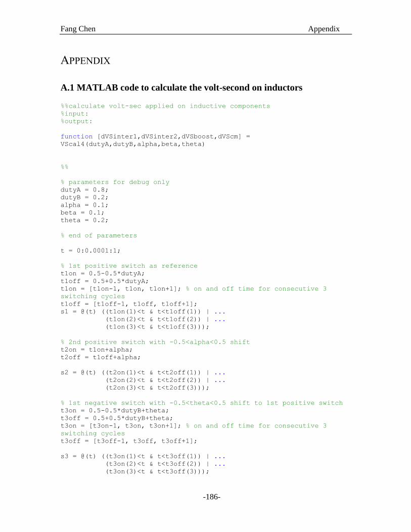
Fang Chen Appendix
-186-
APPENDIX
A.1 MATLAB code to calculate the volt-second on inductors
%%calculate volt-sec applied on inductive components
%input:
%output:
function [dVSinter1,dVSinter2,dVSboost,dVScm] =
VScal4(dutyA,dutyB,alpha,beta,theta)
%%
% parameters for debug only
dutyA = 0.8;
dutyB = 0.2;
alpha = 0.1;
beta = 0.1;
theta = 0.2;
% end of parameters
t = 0:0.0001:1;
% 1st positive switch as reference
t1on = 0.5-0.5*dutyA;
t1off = 0.5+0.5*dutyA;
t1on = [t1on-1, t1on, t1on+1]; % on and off time for consecutive 3
switching cycles
t1off = [t1off-1, t1off, t1off+1];
s1 = @(t) ((t1on(1)<t & t<t1off(1)) | ...
(t1on(2)<t & t<t1off(2)) | ...
(t1on(3)<t & t<t1off(3)));
% 2nd positive switch with -0.5<alpha<0.5 shift
t2on = t1on+alpha;
t2off = t1off+alpha;
s2 = @(t) ((t2on(1)<t & t<t2off(1)) | ...
(t2on(2)<t & t<t2off(2)) | ...
(t2on(3)<t & t<t2off(3)));
% 1st negative switch with -0.5<theta<0.5 shift to 1st positive switch
t3on = 0.5-0.5*dutyB+theta;
t3off = 0.5+0.5*dutyB+theta;
t3on = [t3on-1, t3on, t3on+1]; % on and off time for consecutive 3
switching cycles
t3off = [t3off-1, t3off, t3off+1];
s3 = @(t) ((t3on(1)<t & t<t3off(1)) | ...
(t3on(2)<t & t<t3off(2)) | ...
(t3on(3)<t & t<t3off(3)));
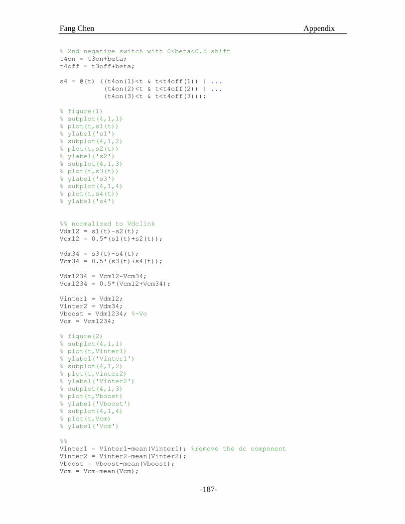
Fang Chen Appendix
-187-
% 2nd negative switch with 0<beta<0.5 shift
t4on = t3on+beta;
t4off = t3off+beta;
s4 = @(t) ((t4on(1)<t & t<t4off(1)) | ...
(t4on(2)<t & t<t4off(2)) | ...
(t4on(3)<t & t<t4off(3)));
% figure(1)
% subplot(4,1,1)
% plot(t,s1(t))
% ylabel('s1')
% subplot(4,1,2)
% plot(t,s2(t))
% ylabel('s2')
% subplot(4,1,3)
% plot(t,s3(t))
% ylabel('s3')
% subplot(4,1,4)
% plot(t,s4(t))
% ylabel('s4')
%% normalized to Vdclink
Vdm12 = s1(t)-s2(t);
Vcm12 = 0.5*(s1(t)+s2(t));
Vdm34 = s3(t)-s4(t);
Vcm34 = 0.5*(s3(t)+s4(t));
Vdm1234 = Vcm12-Vcm34;
Vcm1234 = 0.5*(Vcm12+Vcm34);
Vinter1 = Vdm12;
Vinter2 = Vdm34;
Vboost = Vdm1234; %-Vo
Vcm = Vcm1234;
% figure(2)
% subplot(4,1,1)
% plot(t,Vinter1)
% ylabel('Vinter1')
% subplot(4,1,2)
% plot(t,Vinter2)
% ylabel('Vinter2')
% subplot(4,1,3)
% plot(t,Vboost)
% ylabel('Vboost')
% subplot(4,1,4)
% plot(t,Vcm)
% ylabel('Vcm')
%%
Vinter1 = Vinter1-mean(Vinter1); %remove the dc component
Vinter2 = Vinter2-mean(Vinter2);
Vboost = Vboost-mean(Vboost);
Vcm = Vcm-mean(Vcm);
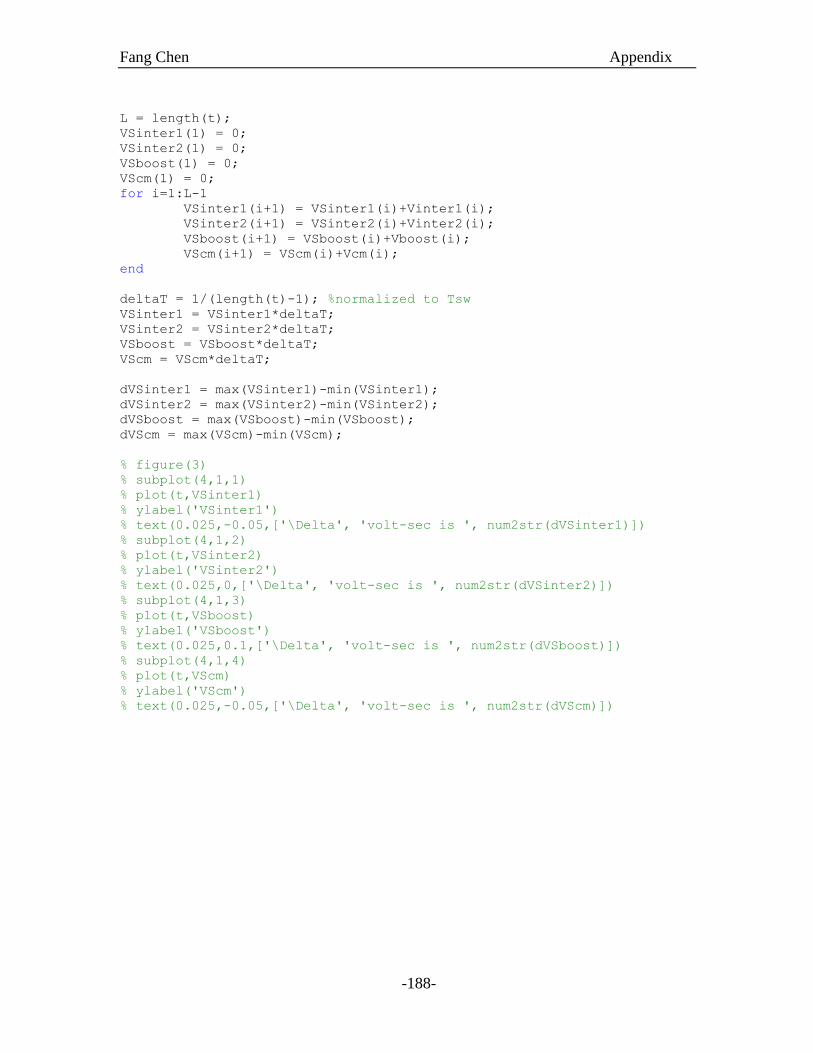
Fang Chen Appendix
-188-
L = length(t);
VSinter1(1) = 0;
VSinter2(1) = 0;
VSboost(1) = 0;
VScm(1) = 0;
for i=1:L-1
VSinter1(i+1) = VSinter1(i)+Vinter1(i);
VSinter2(i+1) = VSinter2(i)+Vinter2(i);
VSboost(i+1) = VSboost(i)+Vboost(i);
VScm(i+1) = VScm(i)+Vcm(i);
end
deltaT = 1/(length(t)-1); %normalized to Tsw
VSinter1 = VSinter1*deltaT;
VSinter2 = VSinter2*deltaT;
VSboost = VSboost*deltaT;
VScm = VScm*deltaT;
dVSinter1 = max(VSinter1)-min(VSinter1);
dVSinter2 = max(VSinter2)-min(VSinter2);
dVSboost = max(VSboost)-min(VSboost);
dVScm = max(VScm)-min(VScm);
% figure(3)
% subplot(4,1,1)
% plot(t,VSinter1)
% ylabel('VSinter1')
% text(0.025,-0.05,['\Delta', 'volt-sec is ', num2str(dVSinter1)])
% subplot(4,1,2)
% plot(t,VSinter2)
% ylabel('VSinter2')
% text(0.025,0,['\Delta', 'volt-sec is ', num2str(dVSinter2)])
% subplot(4,1,3)
% plot(t,VSboost)
% ylabel('VSboost')
% text(0.025,0.1,['\Delta', 'volt-sec is ', num2str(dVSboost)])
% subplot(4,1,4)
% plot(t,VScm)
% ylabel('VScm')
% text(0.025,-0.05,['\Delta', 'volt-sec is ', num2str(dVScm)])
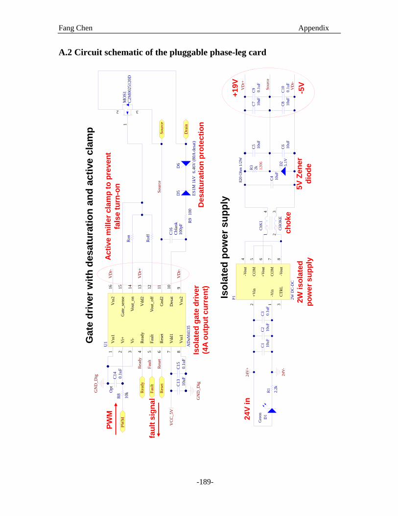
Fang Chen Appendix
-189-
A.2 Circuit schematic of the pluggable phase-leg card
AD
uM
41
35
Vi+
2
Rea
dy
4
Vd
d1
7
Vss
18
Vi-
3V
ou
t_o
n1
4
Vss
29
Des
at1
0
Gn
d2
11
Vd
d2
13
Vss
21
6V
ss1
1
Res
et6
Fau
lt5
Vo
ut_
off
12
Gat
e_se
nse
15
U1
GN
D_
Dig
VC
C_
5V
0.1
uF
C15
10
uF
C13
GN
D_
Dig
VD
r-
VD
r-
Sourc
e
VD
r+
Ron
Ro
ff
10
0p
F
C16
Cbla
nk
D5
ES
1M
1k
V1
00
R9
Dra
in
D6
6.4
6V
(8
0A
des
at)
10
k
R8
0.1
uF
C14
Op
t
Rea
dy
Fau
lt
Res
et
PW
M
Rea
dy
Fau
lt
Sourc
e
2 3
1M
OS
1C
2M
0025120D
Res
et
10
uF
C4
1 234
ChK
1
CH
OK
E
2k
R3
82
0 O
hm
1/2
W
D2
5.1
V1
0u
F
C6
10
uF
C5
VD
r-
VD
r+
10
uF
C2
10
uF
C7
10
uF
C8
0.1
uF
C9
0.1
uF
C10
0.1
uF
C3
Sourc
e
+V
in2
-Vo
ut
4
CO
M5
+V
ou
t6
CO
M7
-Vin
1
CT
RL
3-V
ou
t8
P1
2W
DC
-DC
24
V-
24
V+
10
uF
C1
2.2
k
R1
D1
Gre
en1
20
6
Ga
te d
rive
r w
ith
de
sa
tura
tio
n a
nd
ac
tive
cla
mp
Iso
late
d p
ow
er
su
pp
ly
Acti
ve m
ille
r cla
mp
to
pre
ven
t
fals
e t
urn
-on
Desatu
rati
on
pro
tecti
on
Iso
late
d g
ate
dri
ve
r
(4A
ou
tpu
t cu
rren
t)
24V
in
2W
iso
late
d
po
wer
su
pp
ly
+1
9V
-5V
5V
Zen
er
dio
de
ch
oke
fau
lt s
ign
al
PW
M