Embed Size (px)
Citation preview
Control of Active Component of Current
in Dual Active Bridge Converter
Suyash Sushilkumar Shah∗ and Subhashish Bhattacharya†
Department of Electrical and Computer Engineering
North Carolina State University, Raleigh, NC 27695, USA
Email: ∗[email protected], †[email protected]
Abstract—The paper presents a control strategy based onimproved first harmonic approximation model of the single-phasedual active bridge (DAB) converter. The model consists ofthree state-variables: output DC voltage and two orthogonalcomponents of first harmonic of transformer current, equivalentto active and circulating powers. Foremost, a strategy based onthe conventional output voltage control is designed to regulate theoutput voltage. Subsequently, the first harmonic current controlstrategy, which aims to control the active power component of thecurrent to regulate the output DC voltage, is introduced. Based onthis strategy, a method to design the control system is suggestedand its implementation in digital domain is described. The twocontrol strategies are validated through time-domain simulations.Finally, the schemes are implemented for a prototype 500V/270VDC/DC converter. The experimental results are reported andcompared against the developed control models for verification.
Keywords—Bidirectional dc-dc converter, current control,DAB control, dual active bridge, first harmonic approximation.
NOMENCLATURE
n Turns-ratio of the transformerω Switching frequency (rad/s)Ts Switching cycle period (s)φ Phase-shift between converter-bridge voltagesL Power transfer and leakage inductance (H)C DC-side output capacitance (F)R Load resistance (Ω)vin Input voltage (V)vC Output capacitor voltage (V)iL Secondary side transformer current (A)ℑ〈iL〉1 Active power component of inductor currentℜ〈iL〉1 Circulating power component of inductor currentγ Correction factorGvcφ Plant for output voltage to phase-shift angle, φGvc,ℑ〈iL〉1 Plant for output voltage to ℑ〈iL〉1Gℑ〈iL〉1,φ Plant for ℑ〈iL〉1 to phase-shift angle, φ
I. INTRODUCTION
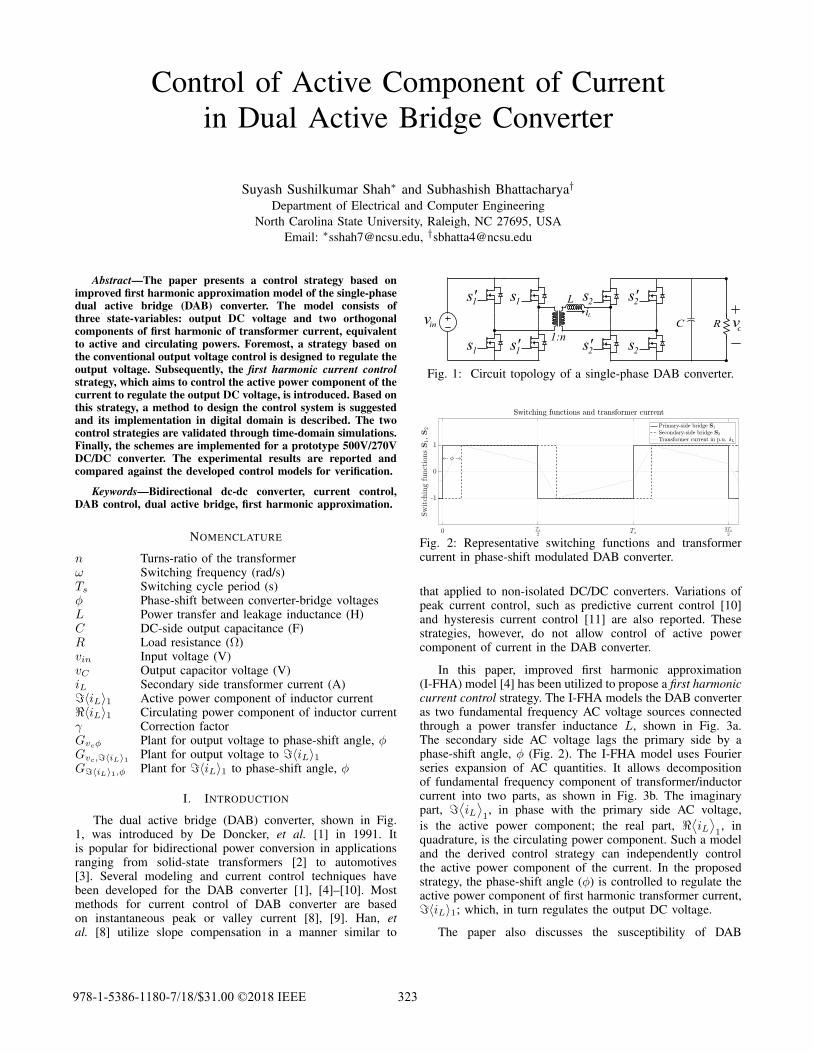
The dual active bridge (DAB) converter, shown in Fig.1, was introduced by De Doncker, et al. [1] in 1991. Itis popular for bidirectional power conversion in applicationsranging from solid-state transformers [2] to automotives[3]. Several modeling and current control techniques havebeen developed for the DAB converter [1], [4]–[10]. Mostmethods for current control of DAB converter are basedon instantaneous peak or valley current [8], [9]. Han, etal. [8] utilize slope compensation in a manner similar to
c v R Cin
v
1 s'
2 s
1s'
1 s
1 s
2 s
2 s'
2 s'
L
L i
1:n
Fig. 1: Circuit topology of a single-phase DAB converter.
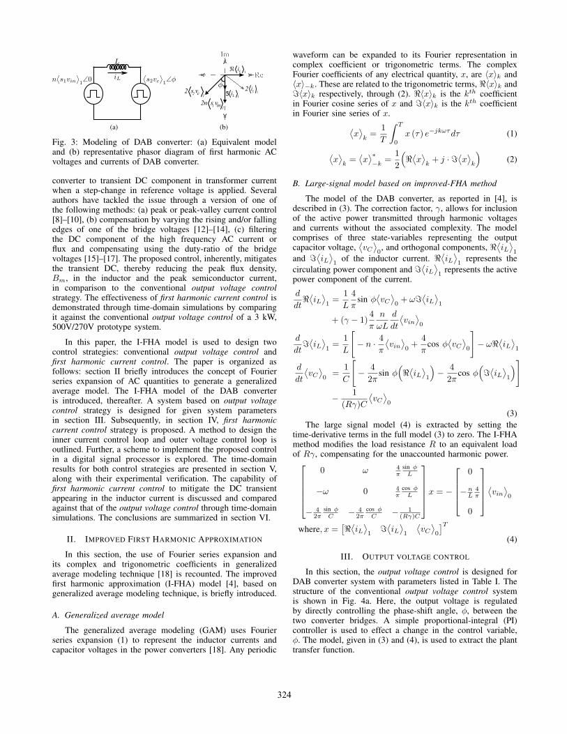
Fig. 2: Representative switching functions and transformercurrent in phase-shift modulated DAB converter.
that applied to non-isolated DC/DC converters. Variations ofpeak current control, such as predictive current control [10]and hysteresis current control [11] are also reported. Thesestrategies, however, do not allow control of active powercomponent of current in the DAB converter.
In this paper, improved first harmonic approximation(I-FHA) model [4] has been utilized to propose a first harmoniccurrent control strategy. The I-FHA models the DAB converteras two fundamental frequency AC voltage sources connectedthrough a power transfer inductance L, shown in Fig. 3a.The secondary side AC voltage lags the primary side by aphase-shift angle, φ (Fig. 2). The I-FHA model uses Fourierseries expansion of AC quantities. It allows decompositionof fundamental frequency component of transformer/inductorcurrent into two parts, as shown in Fig. 3b. The imaginarypart, ℑ
⟨
iL⟩
1, in phase with the primary side AC voltage,
is the active power component; the real part, ℜ⟨
iL⟩
1, in
quadrature, is the circulating power component. Such a modeland the derived control strategy can independently controlthe active power component of the current. In the proposedstrategy, the phase-shift angle (φ) is controlled to regulate theactive power component of first harmonic transformer current,ℑ〈iL〉1; which, in turn regulates the output DC voltage.
The paper also discusses the susceptibility of DAB
978-1-5386-1180-7/18/$31.00 ©2018 IEEE 323
(a)
1in
n s v1
2
2
2 1Li
1Liℑ
1Liℜ
1c
s v2
Im
Re
(b)
Fig. 3: Modeling of DAB converter: (a) Equivalent modeland (b) representative phasor diagram of first harmonic ACvoltages and currents of DAB converter.
converter to transient DC component in transformer currentwhen a step-change in reference voltage is applied. Severalauthors have tackled the issue through a version of one ofthe following methods: (a) peak or peak-valley current control[8]–[10], (b) compensation by varying the rising and/or fallingedges of one of the bridge voltages [12]–[14], (c) filteringthe DC component of the high frequency AC current orflux and compensating using the duty-ratio of the bridgevoltages [15]–[17]. The proposed control, inherently, mitigatesthe transient DC, thereby reducing the peak flux density,Bm, in the inductor and the peak semiconductor current,in comparison to the conventional output voltage controlstrategy. The effectiveness of first harmonic current control isdemonstrated through time-domain simulations by comparingit against the conventional output voltage control of a 3 kW,500V/270V prototype system.
In this paper, the I-FHA model is used to design twocontrol strategies: conventional output voltage control andfirst harmonic current control. The paper is organized asfollows: section II briefly introduces the concept of Fourierseries expansion of AC quantities to generate a generalizedaverage model. The I-FHA model of the DAB converteris introduced, thereafter. A system based on output voltagecontrol strategy is designed for given system parametersin section III. Subsequently, in section IV, first harmoniccurrent control strategy is proposed. A method to design theinner current control loop and outer voltage control loop isoutlined. Further, a scheme to implement the proposed controlin a digital signal processor is explored. The time-domainresults for both control strategies are presented in section V,along with their experimental verification. The capability offirst harmonic current control to mitigate the DC transientappearing in the inductor current is discussed and comparedagainst that of the output voltage control through time-domainsimulations. The conclusions are summarized in section VI.
II. IMPROVED FIRST HARMONIC APPROXIMATION
In this section, the use of Fourier series expansion andits complex and trigonometric coefficients in generalizedaverage modeling technique [18] is recounted. The improvedfirst harmonic approximation (I-FHA) model [4], based ongeneralized average modeling technique, is briefly introduced.
A. Generalized average model
The generalized average modeling (GAM) uses Fourierseries expansion (1) to represent the inductor currents andcapacitor voltages in the power converters [18]. Any periodic
waveform can be expanded to its Fourier representation incomplex coefficient or trigonometric terms. The complexFourier coefficients of any electrical quantity, x, are 〈x〉k and〈x〉−k. These are related to the trigonometric terms, ℜ〈x〉k andℑ〈x〉k respectively, through (2). ℜ〈x〉k is the kth coefficientin Fourier cosine series of x and ℑ〈x〉k is the kth coefficientin Fourier sine series of x.
⟨
x⟩
k=
1
T
∫ T
0
x (τ) e−jkωτdτ (1)
⟨
x⟩
k=
⟨
x⟩∗
−k=
1
2
(
ℜ⟨
x⟩
k+ j · ℑ
⟨
x⟩
k
)
(2)
B. Large-signal model based on improved-FHA method
The model of the DAB converter, as reported in [4], isdescribed in (3). The correction factor, γ, allows for inclusionof the active power transmitted through harmonic voltagesand currents without the associated complexity. The modelcomprises of three state-variables representing the outputcapacitor voltage,
⟨
vC⟩
0, and orthogonal components, ℜ
⟨
iL⟩
1and ℑ
⟨
iL⟩
1of the inductor current. ℜ
⟨
iL⟩
1represents the
circulating power component and ℑ⟨
iL⟩
1represents the active
power component of the current.
d
dtℜ⟨
iL⟩
1=
1
L
4
πsin φ
⟨
vC⟩
0+ ωℑ
⟨
iL⟩
1
+ (γ − 1)4
π
n
ωL
d
dt
⟨
vin⟩
0
d
dtℑ⟨
iL⟩
1=
1
L
[
− n ·4
π
⟨
vin⟩
0+
4
πcos φ
⟨
vC⟩
0
]
− ωℜ⟨
iL⟩
1
d
dt
⟨
vC⟩
0=
1
C
[
−4
2πsin φ
(
ℜ⟨
iL⟩
1
)
−4
2πcos φ
(
ℑ⟨
iL⟩
1
)
]
−1
(Rγ)C
⟨
vC⟩
0
(3)
The large signal model (4) is extracted by setting thetime-derivative terms in the full model (3) to zero. The I-FHAmethod modifies the load resistance R to an equivalent loadof Rγ, compensating for the unaccounted harmonic power.
0 ω 4π
sin φL
−ω 0 4π
cos φL
− 42π
sin φC
− 42π
cos φC
− 1(Rγ)C
x = −
0
−nL
4π
0
⟨
vin⟩
0
where, x =[
ℜ⟨
iL⟩
1ℑ⟨
iL⟩
1
⟨
vC⟩
0
]T
(4)
III. OUTPUT VOLTAGE CONTROL
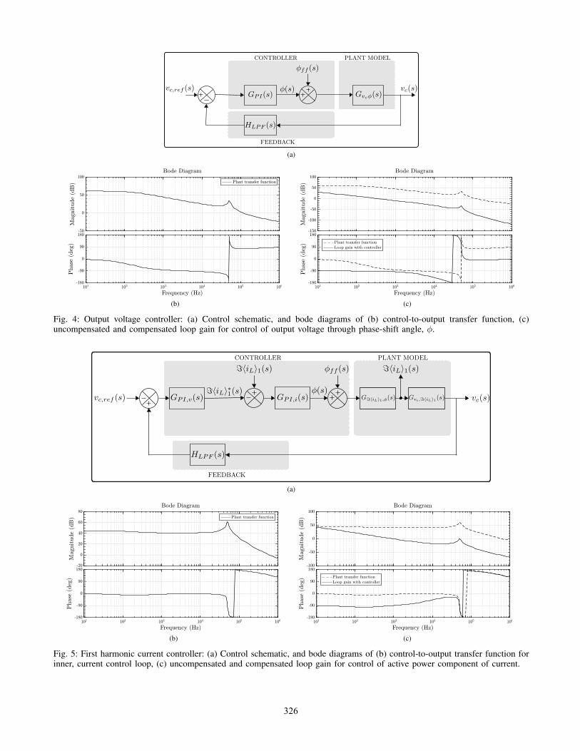
In this section, the output voltage control is designed forDAB converter system with parameters listed in Table I. Thestructure of the conventional output voltage control systemis shown in Fig. 4a. Here, the output voltage is regulatedby directly controlling the phase-shift angle, φ, between thetwo converter bridges. A simple proportional-integral (PI)controller is used to effect a change in the control variable,φ. The model, given in (3) and (4), is used to extract the planttransfer function.
324
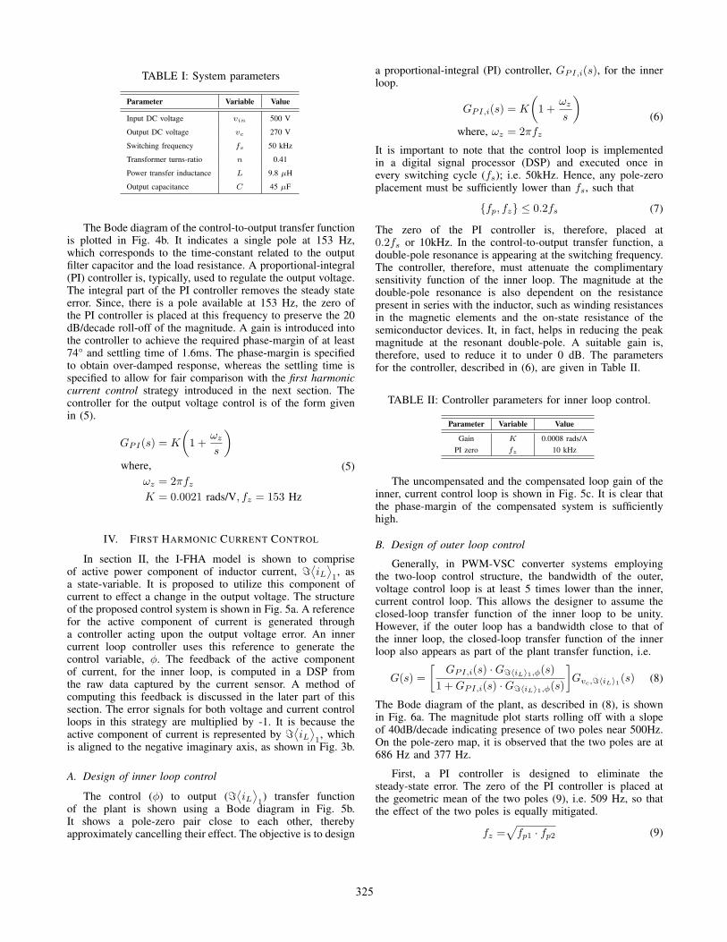
TABLE I: System parameters
Parameter Variable Value
Input DC voltage vin 500 V
Output DC voltage vc 270 V
Switching frequency fs 50 kHz
Transformer turns-ratio n 0.41
Power transfer inductance L 9.8 µH
Output capacitance C 45 µF
The Bode diagram of the control-to-output transfer functionis plotted in Fig. 4b. It indicates a single pole at 153 Hz,which corresponds to the time-constant related to the outputfilter capacitor and the load resistance. A proportional-integral(PI) controller is, typically, used to regulate the output voltage.The integral part of the PI controller removes the steady stateerror. Since, there is a pole available at 153 Hz, the zero ofthe PI controller is placed at this frequency to preserve the 20dB/decade roll-off of the magnitude. A gain is introduced intothe controller to achieve the required phase-margin of at least74° and settling time of 1.6ms. The phase-margin is specifiedto obtain over-damped response, whereas the settling time isspecified to allow for fair comparison with the first harmoniccurrent control strategy introduced in the next section. Thecontroller for the output voltage control is of the form givenin (5).
GPI(s) = K
(
1 +ωz
s
)
where,
ωz = 2πfzK = 0.0021 rads/V, fz = 153 Hz
(5)
IV. FIRST HARMONIC CURRENT CONTROL
In section II, the I-FHA model is shown to compriseof active power component of inductor current, ℑ
⟨
iL⟩
1, as
a state-variable. It is proposed to utilize this component ofcurrent to effect a change in the output voltage. The structureof the proposed control system is shown in Fig. 5a. A referencefor the active component of current is generated througha controller acting upon the output voltage error. An innercurrent loop controller uses this reference to generate thecontrol variable, φ. The feedback of the active componentof current, for the inner loop, is computed in a DSP fromthe raw data captured by the current sensor. A method ofcomputing this feedback is discussed in the later part of thissection. The error signals for both voltage and current controlloops in this strategy are multiplied by -1. It is because theactive component of current is represented by ℑ
⟨
iL⟩
1, which
is aligned to the negative imaginary axis, as shown in Fig. 3b.
A. Design of inner loop control
The control (φ) to output (ℑ⟨
iL⟩
1) transfer function
of the plant is shown using a Bode diagram in Fig. 5b.It shows a pole-zero pair close to each other, therebyapproximately cancelling their effect. The objective is to design
a proportional-integral (PI) controller, GPI,i(s), for the innerloop.
GPI,i(s) = K
(
1 +ωz
s
)
where, ωz = 2πfz
(6)
It is important to note that the control loop is implementedin a digital signal processor (DSP) and executed once inevery switching cycle (fs); i.e. 50kHz. Hence, any pole-zeroplacement must be sufficiently lower than fs, such that
fp, fz ≤ 0.2fs (7)
The zero of the PI controller is, therefore, placed at0.2fs or 10kHz. In the control-to-output transfer function, adouble-pole resonance is appearing at the switching frequency.The controller, therefore, must attenuate the complimentarysensitivity function of the inner loop. The magnitude at thedouble-pole resonance is also dependent on the resistancepresent in series with the inductor, such as winding resistancesin the magnetic elements and the on-state resistance of thesemiconductor devices. It, in fact, helps in reducing the peakmagnitude at the resonant double-pole. A suitable gain is,therefore, used to reduce it to under 0 dB. The parametersfor the controller, described in (6), are given in Table II.
TABLE II: Controller parameters for inner loop control.
Parameter Variable Value
Gain K 0.0008 rads/A
PI zero fz 10 kHz
The uncompensated and the compensated loop gain of theinner, current control loop is shown in Fig. 5c. It is clear thatthe phase-margin of the compensated system is sufficientlyhigh.
B. Design of outer loop control
Generally, in PWM-VSC converter systems employingthe two-loop control structure, the bandwidth of the outer,voltage control loop is at least 5 times lower than the inner,current control loop. This allows the designer to assume theclosed-loop transfer function of the inner loop to be unity.However, if the outer loop has a bandwidth close to that ofthe inner loop, the closed-loop transfer function of the innerloop also appears as part of the plant transfer function, i.e.
G(s) =
[
GPI,i(s) ·Gℑ〈iL〉1,φ(s)
1 +GPI,i(s) ·Gℑ〈iL〉1,φ(s)
]
Gvc,ℑ〈iL〉1(s) (8)
The Bode diagram of the plant, as described in (8), is shownin Fig. 6a. The magnitude plot starts rolling off with a slopeof 40dB/decade indicating presence of two poles near 500Hz.On the pole-zero map, it is observed that the two poles are at686 Hz and 377 Hz.
First, a PI controller is designed to eliminate thesteady-state error. The zero of the PI controller is placed atthe geometric mean of the two poles (9), i.e. 509 Hz, so thatthe effect of the two poles is equally mitigated.
fz =√
fp1 · fp2 (9)
325
CONTROLLER PLANT MODEL
FEEDBACK
(a)
(b) (c)
Fig. 4: Output voltage controller: (a) Control schematic, and bode diagrams of (b) control-to-output transfer function, (c)uncompensated and compensated loop gain for control of output voltage through phase-shift angle, φ.
CONTROLLER PLANT MODEL
FEEDBACK
(a)
(b) (c)
Fig. 5: First harmonic current controller: (a) Control schematic, and bode diagrams of (b) control-to-output transfer function forinner, current control loop, (c) uncompensated and compensated loop gain for control of active power component of current.
326

(a) (b)
(c) (d)
Fig. 6: Outer voltage loop controller design: Bode diagrams of (a) plant transfer function for outer voltage control loop, consideringthe closed loop transfer function of inner current loop, (b) plant transfer function and compensated loop gain with elementaryPI control, (c) control output response to measurement noise with a PI controller followed by a unity gain lead compensator,and (d) plant transfer function and overall compensated loop gain.
The PI control, in conjunction with the poles of the plant,reduces the phase-margin to 21°. A lead compensator is,therefore, used to improve the phase-margin to 60° at across-over frequency of 1 kHz, as shown in Fig. 6b.
The pole and zero for the lead compensator, fp,ld and fz,ld,can be calculated from the following equations.
fm =√
fp,ld · fz,ld
sinφ =fp,ld − fz,ldfp,ld + fz,ld
(10)
Therefore, a lead compensator to increase the phase at fm of1000Hz by φ of 39° with an unity gain magnitude is given by:
Gld(s) =
√
ωz,ld
ωp,ld
1 + s/ωz,ld
1 + s/ωp,ld
where, ωp,ld = 2πfp,ld, ωz,ld = 2πfz,ldand, fp,ld = 2006 Hz, fz,ld = 498 Hz
(11)
The control systems are, generally, designed usingthe compensated loop gain, sensitivity and complementarysensitivity functions. In Fig. 6c, the control output responseto measurement noise is also examined. It shows a magnituderesponse exceeding unity at frequencies in the range of 1-10kHz. It indicates that any measurement noise in the frequencyrange may result in amplified response at the controller
output. If the attenuation due to the plant at this frequency isinsufficient, it may result in unstable or oscillatory response.A suitable gain is, therefore, used to reduce the peak responseof this transfer function to lower than -10dB.
The controller for the outer, voltage loop is given in (12)and the compensated loop gain response is shown in Fig. 6d.
GPI,v(s) = K
(
1 +ωz
s
)(1 + sωz, ld
1 + sωp, ld
)
where, ωz = 2πfz;
ωz,ld = 2πfz,ld and ωp,ld = 2πfp,ld
(12)
TABLE III: Controller parameters for outer loop control.
Parameter Variable Value
Gain K 0.0775 A/V
PI zero fz 509 Hz
Lead zero fz,ld 498 Hz
Lead pole fp,ld 2006 Hz
C. Implementation of inner loop control
The outer voltage control loop is implemented in a DSPin discrete domain using Tustin’s transformation. The innercurrent loop, however, requires extraction of active power
327
(a) (b)
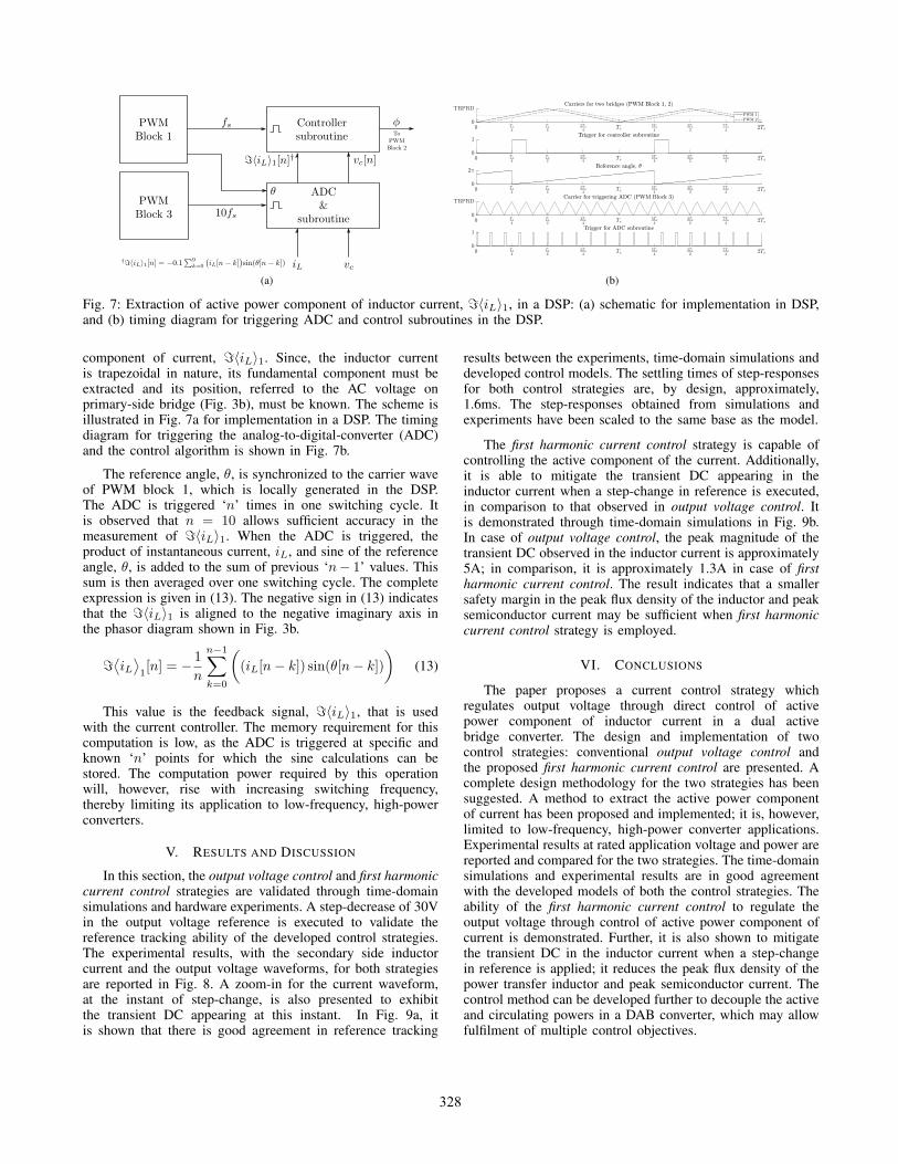
Fig. 7: Extraction of active power component of inductor current, ℑ〈iL〉1, in a DSP: (a) schematic for implementation in DSP,and (b) timing diagram for triggering ADC and control subroutines in the DSP.
component of current, ℑ〈iL〉1. Since, the inductor currentis trapezoidal in nature, its fundamental component must beextracted and its position, referred to the AC voltage onprimary-side bridge (Fig. 3b), must be known. The scheme isillustrated in Fig. 7a for implementation in a DSP. The timingdiagram for triggering the analog-to-digital-converter (ADC)and the control algorithm is shown in Fig. 7b.
The reference angle, θ, is synchronized to the carrier waveof PWM block 1, which is locally generated in the DSP.The ADC is triggered ‘n’ times in one switching cycle. Itis observed that n = 10 allows sufficient accuracy in themeasurement of ℑ〈iL〉1. When the ADC is triggered, theproduct of instantaneous current, iL, and sine of the referenceangle, θ, is added to the sum of previous ‘n− 1’ values. Thissum is then averaged over one switching cycle. The completeexpression is given in (13). The negative sign in (13) indicatesthat the ℑ〈iL〉1 is aligned to the negative imaginary axis inthe phasor diagram shown in Fig. 3b.
ℑ⟨
iL⟩
1[n] = −
1
n
n−1∑
k=0
(
(iL[n− k]) sin(θ[n− k])
)
(13)
This value is the feedback signal, ℑ〈iL〉1, that is usedwith the current controller. The memory requirement for thiscomputation is low, as the ADC is triggered at specific andknown ‘n’ points for which the sine calculations can bestored. The computation power required by this operationwill, however, rise with increasing switching frequency,thereby limiting its application to low-frequency, high-powerconverters.
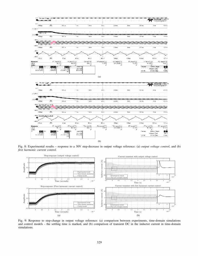
V. RESULTS AND DISCUSSION
In this section, the output voltage control and first harmoniccurrent control strategies are validated through time-domainsimulations and hardware experiments. A step-decrease of 30Vin the output voltage reference is executed to validate thereference tracking ability of the developed control strategies.The experimental results, with the secondary side inductorcurrent and the output voltage waveforms, for both strategiesare reported in Fig. 8. A zoom-in for the current waveform,at the instant of step-change, is also presented to exhibitthe transient DC appearing at this instant. In Fig. 9a, itis shown that there is good agreement in reference tracking
results between the experiments, time-domain simulations anddeveloped control models. The settling times of step-responsesfor both control strategies are, by design, approximately,1.6ms. The step-responses obtained from simulations andexperiments have been scaled to the same base as the model.
The first harmonic current control strategy is capable ofcontrolling the active component of the current. Additionally,it is able to mitigate the transient DC appearing in theinductor current when a step-change in reference is executed,in comparison to that observed in output voltage control. Itis demonstrated through time-domain simulations in Fig. 9b.In case of output voltage control, the peak magnitude of thetransient DC observed in the inductor current is approximately5A; in comparison, it is approximately 1.3A in case of firstharmonic current control. The result indicates that a smallersafety margin in the peak flux density of the inductor and peaksemiconductor current may be sufficient when first harmoniccurrent control strategy is employed.
VI. CONCLUSIONS
The paper proposes a current control strategy whichregulates output voltage through direct control of activepower component of inductor current in a dual activebridge converter. The design and implementation of twocontrol strategies: conventional output voltage control andthe proposed first harmonic current control are presented. Acomplete design methodology for the two strategies has beensuggested. A method to extract the active power componentof current has been proposed and implemented; it is, however,limited to low-frequency, high-power converter applications.Experimental results at rated application voltage and power arereported and compared for the two strategies. The time-domainsimulations and experimental results are in good agreementwith the developed models of both the control strategies. Theability of the first harmonic current control to regulate theoutput voltage through control of active power component ofcurrent is demonstrated. Further, it is also shown to mitigatethe transient DC in the inductor current when a step-changein reference is applied; it reduces the peak flux density of thepower transfer inductor and peak semiconductor current. Thecontrol method can be developed further to decouple the activeand circulating powers in a DAB converter, which may allowfulfilment of multiple control objectives.
328
(a)
(b)
Fig. 8: Experimental results – response to a 30V step-decrease in output voltage reference: (a) output voltage control, and (b)first harmonic current control.
(a) (b)
Fig. 9: Response to step-change in output voltage reference: (a) comparison between experiments, time-domain simulationsand control models - the settling time is marked, and (b) comparison of transient DC in the inductor current in time-domainsimulations.
329

REFERENCES
[1] R. W. A. A. D. Doncker, D. M. Divan, and M. H. Kheraluwala,“A three-phase soft-switched high-power-density DC/DC converter forhigh-power applications,” IEEE Transactions on Industry Applications,vol. 27, no. 1, pp. 63–73, Jan. 1991.
[2] T. Zhao, J. Zeng, S. Bhattacharya, M. E. Baran, and A. Q. Huang,“An average model of solid state transformer for dynamic systemsimulation,” in 2009 IEEE Power Energy Society General Meeting, Jul.2009, pp. 1–8.
[3] J. Walter and R. W. D. Doncker, “High-power galvanically isolatedDC/DC converter topology for future automobiles,” in Power
Electronics Specialist Conference, 2003. PESC ’03. 2003 IEEE 34th
Annual, vol. 1, Jun. 2003, pp. 27–32 vol.1.
[4] S. S. Shah and S. Bhattacharya, “Large & small signal modeling of dualactive bridge converter using improved first harmonic approximation,”in 2017 IEEE Applied Power Electronics Conference and Exposition
(APEC), Mar. 2017, pp. 1175–1182.
[5] N. Soltau, H. A. B. Siddique, and R. W. D. Doncker, “Comprehensivemodeling and control strategies for a three-phase dual-active bridge,”in 2012 International Conference on Renewable Energy Research and
Applications (ICRERA), Nov. 2012, pp. 1–6.
[6] H. Qin and J. Kimball, “Generalized Average Modeling of Dual ActiveBridge DC-DC Converter,” IEEE Transactions on Power Electronics,vol. 27, no. 4, pp. 2078–2084, Apr. 2012.
[7] K. Zhang, Z. Shan, and J. Jatskevich, “Large- and Small-Signal AverageValue Modeling of Dual-active-bridge DC-DC Converter ConsideringPower Losses,” IEEE Transactions on Power Electronics, vol. PP,no. 99, pp. 1–1, 2016.
[8] S. Han, I. Munuswamy, and D. Divan, “Preventing transformersaturation in bi-directional dual active bridge buck-boost DC/DCconverters,” in 2010 IEEE Energy Conversion Congress and Exposition
(ECCE), Sep. 2010, pp. 1450–1457.
[9] J. Huang, Y. Wang, Z. Li, and W. Lei, “Predictive valley-peak currentcontrol of isolated bidirectional dual active bridge DC-DC converter,”in 2015 IEEE Energy Conversion Congress and Exposition (ECCE),Sep. 2015, pp. 1467–1472.
[10] S. Dutta, S. Hazra, and S. Bhattacharya, “A Digital PredictiveCurrent-Mode Controller for a Single-Phase High-FrequencyTransformer-Isolated Dual-Active Bridge DC-to-DC Converter,”IEEE Transactions on Industrial Electronics, vol. 63, no. 9, pp.5943–5952, Sep. 2016.
[11] G. Kunov, I. Iatcheva, D. Marinov, E. Gadjeva, and I. Yatchev,“Bidirectional DAB DC-DC converter with hysteresis current modecontrol,” in 2016 IEEE International Power Electronics and Motion
Control Conference (PEMC), Sep. 2016, pp. 69–74.
[12] K. Takagi and H. Fujita, “Dynamic control and performance of anisolated dual-active-bridge DC-DC converter,” in 2015 9th International
Conference on Power Electronics and ECCE Asia (ICPE-ECCE Asia),Jun. 2015, pp. 1521–1527.
[13] B. Zhao, Q. Song, W. Liu, and Y. Zhao, “Transient DC Bias and CurrentImpact Effects of High-Frequency-Isolated Bidirectional DC-DCConverter in Practice,” IEEE Transactions on Power Electronics,vol. 31, no. 4, pp. 3203–3216, Apr. 2016.
[14] X. Li and Y. F. Li, “An Optimized Phase-Shift Modulation ForFast Transient Response in a Dual-Active-Bridge Converter,” IEEE
Transactions on Power Electronics, vol. 29, no. 6, pp. 2661–2665, Jun.2014.
[15] B. P. Baddipadiga and M. Ferdowsi, “Dual loop control for eliminatingDC-bias in a DC-DC dual active bridge converter,” in 2014 International
Conference on Renewable Energy Research and Application (ICRERA),Oct. 2014, pp. 490–495.
[16] Y. Panov, M. M. Jovanovi, and B. T. Irving, “Noveltransformer-flux-balancing control of dual-active-bridge bidirectionalconverters,” in 2015 IEEE Applied Power Electronics Conference and
Exposition (APEC), Mar. 2015, pp. 42–49.
[17] G. Ortiz, L. Fssler, J. W. Kolar, and O. Apeldoorn, “Flux Balancingof Isolation Transformers and Application of ‘The Magnetic Ear’; forClosed-Loop Volt-Second Compensation,” IEEE Transactions on Power
Electronics, vol. 29, no. 8, pp. 4078–4090, Aug. 2014.
[18] S. R. Sanders, J. M. Noworolski, X. Z. Liu, and G. C. Verghese,“Generalized averaging method for power conversion circuits,” in , 21st
Annual IEEE Power Electronics Specialists Conference, 1990. PESC
’90 Record, 1990, pp. 333–340.
330