Embed Size (px)
Citation preview

Control Interfaces andProcessing System v3.1
LogiCORE IP Product GuideVivado Design Suite
PG352 (v3.1) October 27, 2021
Xilinx is creating an environment where employees, customers, andpartners feel welcome and included. To that end, we’re removing non-inclusive language from our products and related collateral. We’velaunched an internal initiative to remove language that could excludepeople or reinforce historical biases, including terms embedded in oursoftware and IPs. You may still find examples of non-inclusivelanguage in our older products as we work to make these changes andalign with evolving industry standards. Follow this link for moreinformation.

Table of ContentsChapter 1: Introduction.............................................................................................. 4
Features........................................................................................................................................4IP Facts..........................................................................................................................................5
Chapter 2: Overview......................................................................................................6Navigating Content by Design Process.................................................................................... 6Core Overview..............................................................................................................................6Licensing and Ordering.............................................................................................................. 6
Chapter 3: Product Specification........................................................................... 8I/O Peripheral and Flash Memory Controllers........................................................................ 8
Chapter 4: Design Flow Steps.................................................................................10Customizing and Generating the Core...................................................................................10Automation................................................................................................................................ 12CIPS Presets............................................................................................................................... 16CPM............................................................................................................................................. 18Device Integrity......................................................................................................................... 20PS-NoC Interfaces..................................................................................................................... 29Clocking Configuration.............................................................................................................35I/O Configuration...................................................................................................................... 40PL-PS Configuration.................................................................................................................. 44Programmable Logic Interrupts..............................................................................................46Power Configuration.................................................................................................................48Debug Settings.......................................................................................................................... 49Boot Mode..................................................................................................................................53
Appendix A: Upgrading............................................................................................. 55
Appendix B: Debugging.............................................................................................56Finding Help on Xilinx.com...................................................................................................... 56Debug Tools............................................................................................................................... 57
PG352 (v3.1) October 27, 2021 www.xilinx.comCIPS IP Core 2Send Feedback

Appendix C: Additional Resources and Legal Notices............................. 59Xilinx Resources.........................................................................................................................59Documentation Navigator and Design Hubs.........................................................................59References..................................................................................................................................59Revision History......................................................................................................................... 60Please Read: Important Legal Notices................................................................................... 61
PG352 (v3.1) October 27, 2021 www.xilinx.comCIPS IP Core 3Send Feedback

Chapter 1
IntroductionThe Xilinx® Versal® platform Control, Interfaces and Processing System IP is the softwareinterface around the Versal processing system. The Versal family consists of a system-on-chip(SoC) style integrated processing system (PS) and a programmable logic (PL) unit, NoC, and AIEngine providing an extensible and flexible SoC solution on a single die.
Features• Enable/Disable I/O peripherals (IOP)
• Enable/Disable AXI Interfaces
• Multiplexed I/O (MIO) configuration
• Extended multiplexed I/Os (EMIO)
• PL clocks, interrupts, and resets
• Internal clocking (PMC/LPD/FPD)
• Generation of system level configuration registers (SLCRs)
• Enable/Disable PS to/from NoC Interface
• PCIe® and CCIX configuration
• SYSMON configuration
• Debug configuration
Chapter 1: Introduction
PG352 (v3.1) October 27, 2021 www.xilinx.comCIPS IP Core 4Send Feedback

IP FactsLogiCORE™ IP Facts Table
Core Specifics
Supported Device Family Versal® ACAP
Supported User Interfaces AXI4, AXI4-Lite, AXI4-Stream, Native, and NoC
Provided with Core
Design Files Verilog
Example Design Refer block automation for DDR/CPM reference designs
Test Bench N/A
Constraints File N/A
Simulation Model N/A
Supported S/W Driver N/A
Tested Design Flows
Design Entry Vivado® Design Suite
Simulation For supported simulators, see the Xilinx Design Tools: Release Notes Guide.
Synthesis Vivado Synthesis
Support
All Vivado IP Change Logs Master Vivado IP Change Logs: 72775
Xilinx Support web page
Notes:1. For a complete list of supported devices, see the Vivado® IP catalog.2. For the supported versions of the tools, see the Xilinx Design Tools: Release Notes Guide.
Chapter 1: Introduction
PG352 (v3.1) October 27, 2021 www.xilinx.comCIPS IP Core 5Send Feedback

Chapter 2
Overview
Navigating Content by Design ProcessXilinx® documentation is organized around a set of standard design processes to help you findrelevant content for your current development task. All Versal® ACAP design process DesignHubs can be found on the Xilinx.com website. This document covers the following designprocesses:
• Hardware, IP, and Platform Development: Creating the PL IP blocks for the hardwareplatform, creating PL kernels, functional simulation, and evaluating the Vivado® timing,resource use, and power closure. Also involves developing the hardware platform for systemintegration. Topics in this document that apply to this design process include:
• I/O Peripheral and Flash Memory Controllers
• Chapter 4: Design Flow Steps
• Clocking
Core OverviewThe Control Interfaces and Processing System IP core instantiates, boots, and configures theprocessing system section of the Xilinx® Versal® platform.
CIPS is architected as a hierarchical IP encapsulating two sub-IPs namely PS-PMC and CPM IPs.Designing for Versal® always requires at the least the PMC involvement and therefore CIPS to beconfigured.
Licensing and OrderingThis Xilinx® LogiCORE™ IP module is provided at no additional cost with the Xilinx Vivado®
Design Suite under the terms of the Xilinx End User License.
Chapter 2: Overview
PG352 (v3.1) October 27, 2021 www.xilinx.comCIPS IP Core 6Send Feedback

Note: To verify that you need a license, check the License column of the IP Catalog. Included means that alicense is included with the Vivado® Design Suite; Purchase means that you have to purchase a license touse the core.
Information about other Xilinx® LogiCORE™ IP modules is available at the Xilinx IntellectualProperty page. For information about pricing and availability of other Xilinx LogiCORE IP modulesand tools, contact your local Xilinx sales representative.
Chapter 2: Overview
PG352 (v3.1) October 27, 2021 www.xilinx.comCIPS IP Core 7Send Feedback
Chapter 3
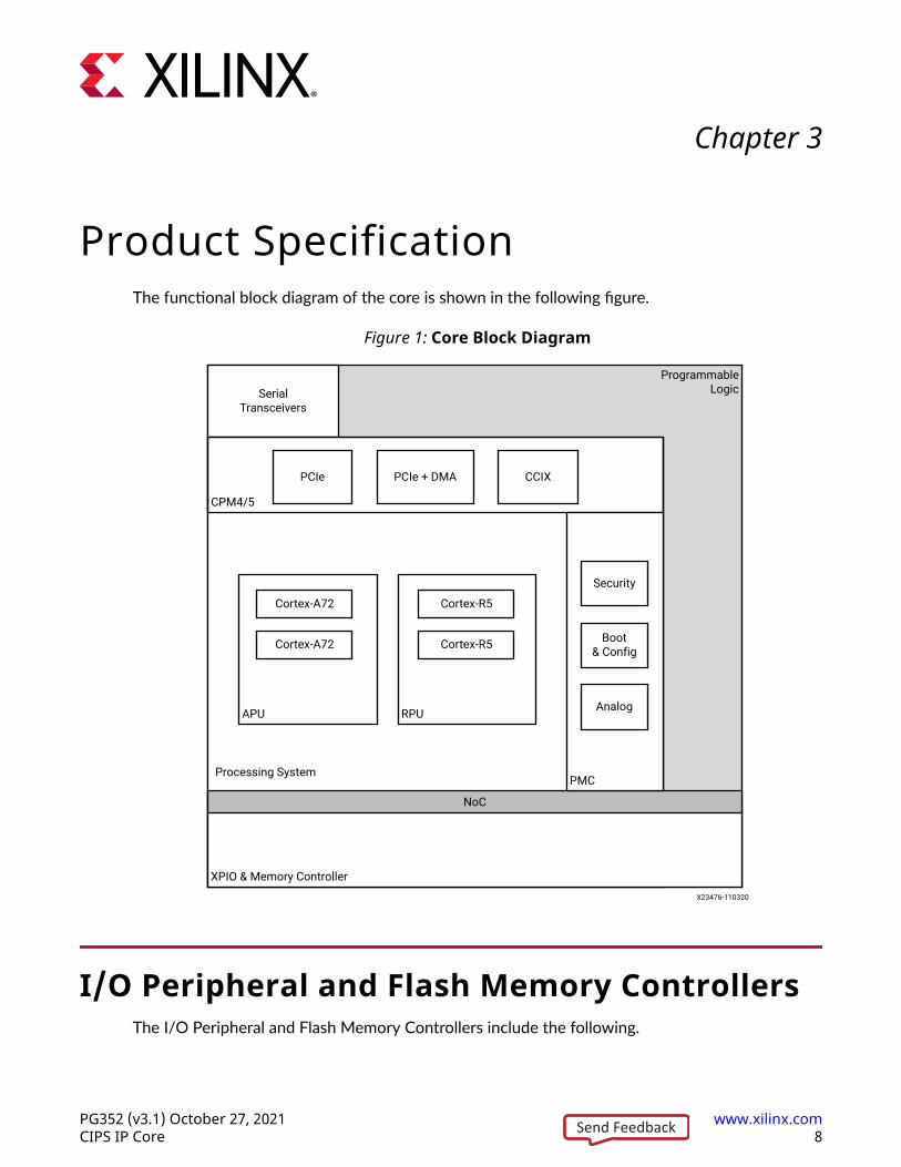
Product SpecificationThe functional block diagram of the core is shown in the following figure.
Figure 1: Core Block Diagram
ProgrammableLogicSerial
Transceivers
XPIO & Memory Controller
NoC
Processing System
CPM4/5
PCIe PCIe + DMA CCIX
PMC
Security
Boot& Config
AnalogAPU RPU
Cortex-A72
Cortex-A72
Cortex-R5
Cortex-R5
X23476-110320
I/O Peripheral and Flash Memory ControllersThe I/O Peripheral and Flash Memory Controllers include the following.
Chapter 3: Product Specification
PG352 (v3.1) October 27, 2021 www.xilinx.comCIPS IP Core 8Send Feedback

• Quad Serial Peripheral Interface (QSPI) flash memory
• Octal Serial Peripheral Interface (OSPI) flash memory
• UART
• I2C
• Serial Peripheral Interface (SPI) flash memory
• SD/eMMC
• General purpose I/O (GPIO)
• Controller Area Network Flexible Data rates (CAN-FD)
• USB 2.0
• Gigabit Ethernet MAC (GEM)
Note: The interfaces for these I/O peripherals (IOPs) can be routed to MIO ports and the extendedmultiplexed I/O (EMIO) interfaces as described in the Versal ACAP Technical Reference Manual (AM011).
• PMC domain peripheral
○ QSPI
○ OSPI
○ 2xSD/eMMC
○ I2C
○ SelectMAP (SMAP)
○ GPIOs
• Low power domain (LPD) peripherals available in PS:
○ 2 X Gigabit Ethernet
○ 1 X USB 2.0
○ 2 X SPI
○ 2 X CAN
○ 2 X I2C
○ 2 X UART
○ GPIOs
Chapter 3: Product Specification
PG352 (v3.1) October 27, 2021 www.xilinx.comCIPS IP Core 9Send Feedback

Chapter 4
Design Flow StepsThis section describes customizing and generating the core, constraining the core, and thesimulation, synthesis, and implementation steps that are specific to this IP core. More detailedinformation about the standard Vivado® design flows and the IP integrator can be found in thefollowing Vivado Design Suite user guides:
• Vivado Design Suite User Guide: Designing IP Subsystems using IP Integrator (UG994)
• Vivado Design Suite User Guide: Designing with IP (UG896)
• Vivado Design Suite User Guide: Getting Started (UG910)
• Vivado Design Suite User Guide: Logic Simulation (UG900)
Customizing and Generating the CoreThis section includes information about using Xilinx® tools to customize and generate the core inthe Vivado® Design Suite.
If you are customizing and generating the core in the Vivado IP integrator, see the Vivado DesignSuite User Guide: Designing IP Subsystems using IP Integrator (UG994) for detailed information. IPintegrator might auto-compute certain configuration values when validating or generating thedesign. To check whether the values do change, see the description of the parameter in thischapter. To view the parameter value, run the validate_bd_design command in the Tclconsole.
You can customize the IP for use in your design by specifying values for the various parametersassociated with the IP core using the following steps:
1. Select the IP from the IP catalog.
2. Double-click the selected IP or select the Customize IP command from the toolbar or right-click menu.
For details, see the Vivado Design Suite User Guide: Designing with IP (UG896) and the VivadoDesign Suite User Guide: Getting Started (UG910).
Figures in this chapter are illustrations of the Vivado IDE. The layout depicted here might varyfrom the current version.
Chapter 4: Design Flow Steps
PG352 (v3.1) October 27, 2021 www.xilinx.comCIPS IP Core 10Send Feedback

CIPS IP Core Block DesignYou can customize the Control Interfaces and Processing System IP core by clicking on the CIPSIP. The block diagram on selecting the customization is shown in the following figure.
Figure 2: CIPS IP Core Block Design
Choosing a Design FlowCIPS is a very flexible and can be configured in several different ways. CIPS IP enablesconfiguration of many operating parameters. There are two Design Flows available forconfiguring these parameters. The two flows, based on the archetype of the two traditional userpersona, guide the user as per the predetermined presets. These two flows do not alter theexpert users complete freedom in the configuration order and options. They are in fact anaddition to help and guide the user.
Chapter 4: Design Flow Steps
PG352 (v3.1) October 27, 2021 www.xilinx.comCIPS IP Core 11Send Feedback

Table 1: CIPS Design Flows
Design Flow DescriptionPL Subsystem This flow configures only the vital components to use the
programmable logic (PL) domain of the Versal device. Whenthis flow is selected, only the Platform ManagementController (PMC) is configured as it is necessary forinitialization of the Versal ACAP.
Note: All other device domains (For example, PS or CPM) aredisabled in this flow.
For example, if the design targets the programmable logicexclusively and does not use any other domain, select thisflow.
Full System This flow configures all domains on the Versal ACAP. Allavailable domains on the device will be shown and availablefor configuration.
AutomationThe CIPS IP is supported by Vivado IP integrator optional assistance to the designer such asBlock and Board Automation. Block Automation provides an initial configuration and connects toadditional related IP blocks. Board Automation applies a specific configuration preset to CIPS IPwhen a board part is chosen and has a preset. Therefore the CIPS IP settings are customized towork with the targeted board.
In addition, other IPs may provide Connection Automation for additional peripheral/connectivityto be connected to CIPS IP. Following are the automation limitations:
• Block, board, and connection automation are independent entities in the IP integrator. Usingmultiple automations may cause conflicts.
• Connection Automation may not recognize hardened interfaces.
• Block Automation is not reentrant. It cannot be invoked twice unless the IP is removed fromIP integrator and added again.
Block AutomationVivado® supports the Block Automation for Control, Interfaces and Processing System IP to aidin integrating it into the larger design. After adding the CIPS IP to the block diagram, the blockautomation banner pops up. Click Run Block Automation to open the block automation page.
Chapter 4: Design Flow Steps
PG352 (v3.1) October 27, 2021 www.xilinx.comCIPS IP Core 12Send Feedback
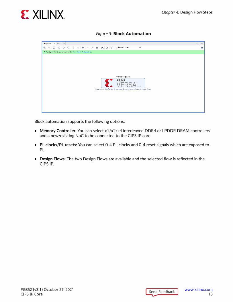
Figure 3: Block Automation
Block automation supports the following options:
• Memory Controller: You can select x1/x2/x4 interleaved DDR4 or LPDDR DRAM controllersand a new/existing NoC to be connected to the CIPS IP core.
• PL clocks/PL resets: You can select 0-4 PL clocks and 0-4 reset signals which are exposed toPL.
• Design Flows: The two Design Flows are available and the selected flow is reflected in theCIPS IP.
Chapter 4: Design Flow Steps
PG352 (v3.1) October 27, 2021 www.xilinx.comCIPS IP Core 13Send Feedback

Figure 4: Run Block Automation
When you click OK, a validate ready design is provided with input requirements.
Note: The block automation banner disappears when CIPS IP instance configuration is updated/changed.Thus, it must be the first configuration step if intended to be used.
Board AutomationWhen you create a Vivado® project targeting a board instead of a specific device, a board presetmay be available to initialize the CIPS IP core with board-specific settings.
After instantiating the CIPS IP in the block design, a green banner will appear indicating thatdesigner assistance is available. To access board automation, click Run Block Automation on thisbanner.
To set the board preset, set Apply Board Preset to Yes in the Run Block Automation window.
IMPORTANT! If Apply Board Preset is set to No and block automation is run, the board preset will not beapplied. Ensure to manually enable peripherals on the Peripherals and I/O Configuration pages.
Chapter 4: Design Flow Steps
PG352 (v3.1) October 27, 2021 www.xilinx.comCIPS IP Core 14Send Feedback

TIP: For ensuring flexibility, Vivado IP integrator provides a board tab available in the Data Windows Area,where the various board presets are also available and can be dragged and dropped on the canvas.
Figure 5: Applying the Board Automation Using Block Automation
IMPORTANT! Using the Board window in IP integrator to drag the External Memory DDR4 or LPDDR4interfaces onto the block design canvas does not applies the board preset and the connections to thememory controllers in the NoC are not external. Execute the following procedure to apply boardautomation to DDR4 or LPDDR4:
1. Open CIPS Block Automation window.
2. Select the desired Memory Controller Type and click Ok.
3. Verify that the selected memory controller is added to the block design canvas and the boardpreset is applied.
Chapter 4: Design Flow Steps
PG352 (v3.1) October 27, 2021 www.xilinx.comCIPS IP Core 15Send Feedback
CIPS PresetsCIPS is enabled with default configurations for CIPS parameters referred as Presets. The Presetsfacilitate design creation and block automation and enable users to quickly configure the IPthrough GUI without digging into parameter details. Different Presets are available based on theselected Design Flow. The default Presets represent the simplest and necessary options to setup. The options are based on traditional, most encountered use-cases, and on device minimalboot and run-time requirements.
There are two Design Flows available namely PL Subsystem and Full System. On the basis of theDesign Flow selected, the default Presets configurations are enabled into selected parameter.
TIP: It allows changing Presets value by user at later stage in PS PMC and CPM windows.
Clicking Apply Configuration in Presets enables user to import presets through Presets Tclfile.
Enabled Presets provides a summary of selected parameters for configuration.
Having Presets in CIPS ensures minimum amount of steps required to achieve the configurationneeded for their flow.
• PL Subsystem: It stands for PMC + PL where no Processing System is used. It is aimed attraditional FPGA designers, with no to limited interest in the Processing system. This is whysome presets are grayed out in PL Subsystem but enabled in Full System Configuration.
• Full System: It stands for PS + PMC + CPM + PL and is aimed at the Embedded designer witha definitive interest in PS and/or CPM configuration and interaction with DDR and potentialinteraction with PL. The advanced user can select the Full System Design Flow and potentiallysome presets, but can skip the presets. Click the Next button to access the PS PMC and CPMIPs within CIPS to configure them. It is aimed at an advanced user with knowledge above whatis expected as standard.
The presets configurations applied are then visible within the PS PMC IP by clicking Next andaccessing the detailed settings within the PS PMC Sub-IP.
Note: The Presets set to Custom do not apply any configuration.
The PS-PMC sub-IP exposes all the details and options hidden in the Presets. Presets can beused as a basis to then tune the configuration further. IO Pins allocations and conflicts resolutionare easily achieved through one and only one panel. The IO panel which provides a general viewof the interfaces currently selected to leverage MIOs and their respective MIO pins layout. AnyMIO conflict is highlighted in red.
Chapter 4: Design Flow Steps
PG352 (v3.1) October 27, 2021 www.xilinx.comCIPS IP Core 16Send Feedback

Figure 6: Presets in CIPS
The following are the Presets available in CIPS module:
• Board Interface Configures default boot mode and the default set of peripherals and clocksfound on the selected board part when ps pmc fixed io is selected.
TIP: This is only visible when Full System design flow is selected.
• Boot Configuration Selects boot configuration from Master, Slave, JTAG, or Custom.
• Clock Settings Sets the system reference clock frequency REF_CLK to 33.33 MHz.
• Connectivity to MC via NoC Enables the dedicated connectivity that can be used to connectto a NoC instance with a memory controller.
• IO Peripherals
TIP: This is not applicable when PL Subsystem is selected in the Design Flow.
Chapter 4: Design Flow Steps
PG352 (v3.1) October 27, 2021 www.xilinx.comCIPS IP Core 17Send Feedback

As JTAG is always available on Versal, the Debug preset set to custom or JTAG has no effectand defaults to JTAG support via DAP.
• Debug Selects one of the debug option from JTAG, HIGH Speed Debug Port (HSDP), orCustom.
• Device Integrity Enables you to monitor and respond to the system operating conditions andexceptional events.
• PS PL Connectivity Selects Single FPD and Master/Slave LPD clock.
TIP: This is not applicable when PL Subsystem is selected in the Design Flow.
CPMThe Control, Interfaces and Processing System IP core is also used to configure the PCIe®
module. There are direct interfaces to the CPM, which includes a complete subsystem for PCIe.Certain devices do not offer CPM, while others which do offer either a CPM4 or a CPM5 versionof this block.
Note: Currently, only the Full System (PS + PMC + CPM + PL) flow supports PCIe® configurations in theCPM block.
Chapter 4: Design Flow Steps
PG352 (v3.1) October 27, 2021 www.xilinx.comCIPS IP Core 18Send Feedback

Figure 7: CPM4 Basic Configuration
Chapter 4: Design Flow Steps
PG352 (v3.1) October 27, 2021 www.xilinx.comCIPS IP Core 19Send Feedback

Figure 8: CPM5 Basic Configuration
Note: For more information on CPM module, see Versal ACAP CPM Mode for PCI Express Product Guide(PG346), Versal ACAP CPM DMA and Bridge Mode for PCI Express Product Guide (PG347), and Versal ACAPCPM CCIX Architecture Manual (AM016).
Device IntegrityThe Device integrity feature enable users to monitor and respond to the system operatingconditions and exceptional events. Many of these features are broadly applicable to manydesigns, while others are provided in support of meeting stringent reliability, security, and safetyrequirements. Device integrity has three modules namely, SYSMON, XilSEM Library, and Tamperconfigurations as described in subsequent sections.
Chapter 4: Design Flow Steps
PG352 (v3.1) October 27, 2021 www.xilinx.comCIPS IP Core 20Send Feedback

System MonitorThe System Monitor (SYSMON) enables monitoring of the physical environment both within theVersal® ACAP itself and also within the wider system using the external inputs. It is used toensure that both the Versal ACAP and the overall system operate in a safe, secure, and reliableway. The SYSMON provides the customer with a digital measure of the temperature and appliedvoltage supplies as well as off-chip voltage measurements within the broader system context.Off-chip, its main uses are for board level monitoring of supply voltages/currents.
The Control, Interfaces and Processing System IP core can enable the following measurements:
• On-chip Supply Monitor
• Temperature Measurements
• External Supply Measurements
The Basic Configuration tab has Default and Custom options, as shown in the following figure.
Chapter 4: Design Flow Steps
PG352 (v3.1) October 27, 2021 www.xilinx.comCIPS IP Core 21Send Feedback

Figure 9: SYSMON Basic Configuration
The default window has different preset options to provide a common starting point for typicalSYSMON usage. Each measurement has associated threshold levels which control alarmassertion. The alarms are enabled by default. For external access to SYSMON measurements,I2C, and PMBus interfaces are supported.
The default window also provides the option for setting the voltage averaging levels of 2, 4, 8,and 16. The MIO pin allocation can be modified through the IO panel. Any MIO conflict ishighlighted with icon.
On-Chip Supply Monitor
The On-chip supply monitor tab supports different types of voltage measurements includingcustomer supply voltages and customer dedicated pad voltages.
Chapter 4: Design Flow Steps
PG352 (v3.1) October 27, 2021 www.xilinx.comCIPS IP Core 22Send Feedback

The On Chip Supply Monitor configuration is shown in the following figure.
Figure 10: On Chip Supply Monitor
The CIPS IP core allows you to enable averaging, define the ADC Mode (unipolar/bipolar), andenable alarms with user-defined upper and lower thresholds.
Temperature Measurements
The Temperature configuration tab configures device temperature monitoring options, includingover-temperature shutdown. Alarms are all specified in window mode, where the alarm isasserted above the upper threshold or blow the lower threshold. You can configure the lower andupper temperature value based on the design requirements.
Chapter 4: Design Flow Steps
PG352 (v3.1) October 27, 2021 www.xilinx.comCIPS IP Core 23Send Feedback

Figure 11: Temperature Configuration
External Supply Measurements
The Control, Interfaces and Processing System IP core allows up to 16 pins to be selected forexternal supply measurements. All AUXIOs should be assigned to the same bank.
For example, if AUX_IO_P is LPD Bank MIO0 (VCCO_502 rail), then AUX_IO_N should beassigned from LPD MIO Bank MIO (VCCO_502 rail).
The AUXIOs supports PMC MIOs, LPD MIOs, and HDIOs. But PMC and LPD MIOs may haveconflict based on PS-PMC IO Configuration page. To resolve the conflict, use other free availableIOs.
The External Supply monitor configuration tab is shown in the following figure:
Chapter 4: Design Flow Steps
PG352 (v3.1) October 27, 2021 www.xilinx.comCIPS IP Core 24Send Feedback

Figure 12: SYSMON External Supply Monitor
XilSEM Library ConfigurationThe Xilinx Soft Error Mitigation (XilSEM) library provides a pre-configured and pre-verifiedsolution to detect and optionally correct soft errors in Configuration Memory of Versal ACAPs.The fundamental feature of the XilSEM Library can be enabled in CIPS. This features soft errormitigation of Configuration RAM through a scan-based process automated by integrated logic. Itis managed by the XilSEM Library which reads back Configuration RAM and uses ECC and CRCto detect and correct soft errors. If this feature is enabled in CIPS, the default behavior is to beginoperation automatically after boot. The following figure shows the fundamental featureaccessible through the XilSEM Library configuration section of the CIPS GUI.
Chapter 4: Design Flow Steps
PG352 (v3.1) October 27, 2021 www.xilinx.comCIPS IP Core 25Send Feedback

Figure 13: XilSEM Library Configuration
Advanced features of the XilSEM Library can be accessed through properties applied to thedesign. The XilSEM Library provides an optional feature for the soft error mitigation of NPIRegisters, provided the supplemental hardware resources required for this feature are accessible.This feature is a scan-based process automated by integrated logic and managed by the XilSEMLibrary, which reads back NPI Registers and uses SHA to detect errors. For more information, seeOS and Libraries Document Collection (UG643).
Tamper Events/Response ConfigurationTamper events are interrupts from a tamper monitoring function and user can select differentresponses to each tamper events.
Chapter 4: Design Flow Steps
PG352 (v3.1) October 27, 2021 www.xilinx.comCIPS IP Core 26Send Feedback

Figure 14: Tamper Response System
Tamper monitoring system in CIPS generates interrupts as an when it detects below events.
• Supply Glitch: Whenever there is a glitch in power supply happens, then this event will getgenerated. Glitching the power supply (low or high) can cause insecurely designed statemachines to skip states. Glitches are injected at various points in time and vary in pulsewidths.
• Temperature Deviation: When device temperature goes out of specification (high or low) thenthis event will be generated. This is commonly done in conjunction with a voltage attack. Bothlow and high temperature cause race conditions that can trip just about any type of circuity.
• Debug (JTAG) toggle detect: Debug interfaces attack the Silicon devices, most frequently thisis the JTAG port but with the growing complexity of devices more advanced debug interfacesare becoming more prominent. This event would be generated when there is a toggle in debuginterfaces.
• Custom User (External MIO) event: This event is generated when Tamper monitoring systemdetects any interrupt (active-High) on external MIO.
• Tamper Register event: When you directly trigger the tamper system by writing to its specificregister, then this event would be generated.
CIPS has different responses to each of the above mentioned tamper events, which are describedbelow.
• BBRAM Zeroization: When a tamper event is detected, it is required that the you canimmediately erase the key stored in BBRAM. However, in high grade crypto applications, it isnot sufficient to simply delete the key when done or when a tamper event is detected. It isrequired to be zeroized (erase + verify). CIPS provides this response for all the tamper events.
Chapter 4: Design Flow Steps
PG352 (v3.1) October 27, 2021 www.xilinx.comCIPS IP Core 27Send Feedback

• Secure Lockdown: Upon detection of a tamper event, you want the system to go into someform of lockdown state. CIPS provides lockdown response for all the tamper events.
• Secure Lockdown (With IO Tristate): Some systems require a more severe response to atamper event and even secure lockdown is not enough. It such cases it is necessary to alsotristate all IO to the device. This makes it impossible for the adversary to gain any level ofaccess to the device after a tamper event. CIPS provides lockdown with IO Tristate responsefor all the tamper events.
• System Reset: You may want to only Reset the system, upon receiving the tamper event. CIPSprovides System Reset response for all the tamper events.
• System Interrupt: You may only want to know that the tamper event is occurred. Tamperresponse system generates an interrupt to system, upon receiving any tamper event.
You can select BBRAM Zeroization or Secure Lockdown or Secure Lockdown (With IO Tristate) orSystem Reset or System Interrupt for each Tamper Event as response in PCW.
Figure 15: Tamper Events/Response Configuration
Chapter 4: Design Flow Steps
PG352 (v3.1) October 27, 2021 www.xilinx.comCIPS IP Core 28Send Feedback

PS-NoC InterfacesThe PS-NoC Interfaces tab enables memory-mapped connectivity from the Control, Interfacesand Processing System processors to other Versal® device resources such as DDR, AI Engine, andPL.
The following table lists the NoC interfaces from which you can select in the customization core.
Table 2: List of NoC Interfaces
Interface Name Size Notes4 NoC Master Ports 128-bit channels PS-CCI → NoC channels
2 NoC Master Ports 128-bit channels PS-NCI → NoC channels
1 NoC Master Ports 128-bit channels PS-LPD (RPU) → NoC channels
1 NoC Master Ports 128-bit channels PMC/Debug → NoC channels(via LPD)
2 NoC Master Ports 128-bit channels CPM4/5 (PCIe/CCIX) → NoC channels (via LPD)
4 NoC Slave Ports 128-bit channels NoC → PS channels (2 go to CCI, 2 go to NCI)
1 NoC Slave Ports 128-bit channels NoC → PS-LPD/PMC channels
1 NoC Slave Ports 128-bit channels NoC → PCIe/CCIX/CPM4/5 channels (via LPD)
The CIPS IP core for the NoC interface selection is shown in the following figure.
Chapter 4: Design Flow Steps
PG352 (v3.1) October 27, 2021 www.xilinx.comCIPS IP Core 29Send Feedback

Figure 16: PS-NoC Interfaces
The following are a few recommendations on the usage of PS-NoC ports.
• If any design has AI Engine then you must enable PMC NoC port for AI Engine configuration.
• By default, the 32-bit RPU is unable to access or control the AI Engine at its >32-bit address.This access can be enabled by remapping the entire LPD_AXI_NOC_0 address range of theupper 1GB of DDR LOW0 region (0x40000000 to 0x7FFFFFFF) to the AI Engine for all LPDmasters with the Tcl command (assuming axi_noc_0 is the NoC instance name, andLPD_AXI_NOC is connected to S00_AXI, and the AI Engine IP is connected to M00_AXI):
set_property CONFIG.REMAPS {M00_AXI {0x4000_0000 0x200_0000_0000 1G}} [get_bd_intf_pins /axi_noc_0/S00_AXI]
If any LPD masters such as LPDMA, GEM, or USB DMA still want to access the full DDR atthis range, these masters transactions must be routed through the FPD.
Chapter 4: Design Flow Steps
PG352 (v3.1) October 27, 2021 www.xilinx.comCIPS IP Core 30Send Feedback

Note: Following is the Tcl command to enable the route through FPD support for LPD Masters:
set_property -dict [list CONFIG.PS_PMC_CONFIG {PMC_SD0_ROUTE_THROUGH_FPD 1 PMC_SD1_ROUTE_THROUGH_FPD 1 PMC_OSPI_ROUTE_THROUGH_FPD 1 PMC_QSPI_ROUTE_THROUGH_FPD 1 PS_USB_ROUTE_THROUGH_FPD 1 PS_GEM0_ROUTE_THROUGH_FPD 1 PS_GEM1_ROUTE_THROUGH_FPD 1 PS_LPDMA0_ROUTE_THROUGH_FPD 1 PS_LPDMA1_ROUTE_THROUGH_FPD 1 PS_LPDMA2_ROUTE_THROUGH_FPD 1 PS_LPDMA3_ROUTE_THROUGH_FPD 1 PS_LPDMA4_ROUTE_THROUGH_FPD 1 PS_LPDMA5_ROUTE_THROUGH_FPD 1 PS_LPDMA6_ROUTE_THROUGH_FPD 1 PS_LPDMA7_ROUTE_THROUGH_FPD 1}] [get_bd_cells versal_cips_0]
• All 4 PS to NoC CCI ports must connect to the NoC.
NoC InterfacesThe following is the list of interfaces between PS/PMC and NoC. You can select these in the NoCinterfaces section to communicate with the DDR/PL/AIE.
• Coherent (CCI) master ports: The CIPS IP core has four coherent master ports(FPD_CCI_NOC_0,1,2,3) connected from PS-CCI to NoC. CCI drives these ports ininterleaving mode (2 ports and 4 ports), so you must connect all 4 ports to NoC to access anyslave. The CIPS core masters A72/R5/PMC/DMA can make use of these ports. Also, PLmasters that are connected to CIPS on CCI slave ports can access these ports.
• Non-Coherent (NCI) master ports: The CIPS core has two non-Coherent master ports(FPD_AXI_NOC_0,1). Only PL masters which are connected to NCI slave ports of the CIPScore can access these ports.
TIP: Coherency is NOT enabled by default at boot on the CCI AXI-Lite ports.
• LPD (RPU) master port: There is one master port from LPD (NOC_LPD_AXI_0) to NoC. LPDmasters RPU/DMA can make use of this master port to access slaves.
• PMC master port: The CIPS core has one master port (PMC_NOC_AXI_0) from PMC domainto NoC. This port is used by PMC for debug/boot.
• CPM4/5 master ports: Two master ports (IF_PS_NOC_PCIE_0,1) are exposed from the CIPScore. One is connected to PCIe0 controller and the other is to CCIX module. CPM4/5 canaccess DDR/PL/AIE regions using these ports. You can select connected ports in the CPM4/5Configuration page.
Chapter 4: Design Flow Steps
PG352 (v3.1) October 27, 2021 www.xilinx.comCIPS IP Core 31Send Feedback

• Coherent (CCI) Slave ports: The CIPS core has two coherent slave ports (NOC_FPD_CCI_0,1).Masters connected to these ports can achieve coherency and virtualization. Mastersconnected to these ports can access DDR, PL slaves which are connected to CIPS via CCIports. Also PL masters have access to CIPS internal memory regions.
• Non-Coherent (NCI) Slave ports: The CIPS core has two non-coherent slave ports(NOC_FPD_AXI_0,1). Masters connected to these ports can achieve only virtualization. PLmasters connected to these ports can access DDR, PL slaves which are connected to CIPS viaNCI ports. Also PL masters have access to CIPS internal memory regions.
• PMC/LPD Slave port: There is one slave port (NOC_PMC_AXI_0) to LPD/PMC region. PLmasters connected to this port will get access to these regions.
• CPM4/5 Slave port: The CIPS core has one NoC slave port (IF_NOC_PS_PCIE_0) connectedto CPM4/5 module. External masters can connect to this port to configure the CPM4/5. Youcan select this port in the CPM4/5 Configuration page.
Figure 16: PS-NoC Interfaces shows different NoC master/slave port options to enable theseports.
The following table shows the addresses you can assign to DDR/AI Engine/PL slaves which areconnected to CIPS master NoC ports. For more information on NoC address ranges andconfiguration, see Versal ACAP Programmable Network on Chip and Integrated Memory ControllerLogiCORE IP Product Guide (PG313).
Table 3: NoC Region Address
Slave Region Start Address Size
DDR
Low0 0x0 2 GB
Low1 0x800000000 32 GB
Low2 0xC000000000 256 GB
Low3 0x10000000000 734 GB
CH1 0x50000000000 1 TB
CH2 0x60000000000 1 TB
CH3 0x70000000000 1 TB
PLPLNOC2 TB 0x20100000000 2044 GB
PLNOC8 TB 0x80000000000 8 TB
AI Engine AIE_0 0x20000000000 4 TB
The following figures describe CIPS + DDR + PL slave connections on NoC:
Chapter 4: Design Flow Steps
PG352 (v3.1) October 27, 2021 www.xilinx.comCIPS IP Core 32Send Feedback

Figure 17: CIPS NoC
Figure 18: NoC General Configuration
Chapter 4: Design Flow Steps
PG352 (v3.1) October 27, 2021 www.xilinx.comCIPS IP Core 33Send Feedback

Figure 19: NoC Slave Ports Configuration
Figure 20: NoC Master Ports Configuration
Chapter 4: Design Flow Steps
PG352 (v3.1) October 27, 2021 www.xilinx.comCIPS IP Core 34Send Feedback

Figure 21: NoC Connectivity Configuration
Clocking ConfigurationThis page enables you to configure the peripheral clocks, PL clocks, DDR memory, AI Engine, andCPU clocks. For an overview of the reference clocks used to generate the available clocks see theClock Distribution Diagram in the Versal ACAP Technical Reference Manual (AM011).
ClockingThere are three clock groups as follows.
• Main Clock Group (MCG). This group has the following PLLs:
○ RPU PLL
○ APU PLL
○ PMC PLL
○ NoC PLL
○ CPM4/5 PLL
• RTC Clock Group (RCG). This is a real-time clock, and a dedicated internal clock for RTC. Aclock divider is not required for this clock.
Chapter 4: Design Flow Steps
PG352 (v3.1) October 27, 2021 www.xilinx.comCIPS IP Core 35Send Feedback

• Interface Clock Group (ICG). This group has clocks that are provided externally, like the clocksfrom the physical-side interface (PHY) and PL.
Note: PL side peripherals can be operated through a PL clock (PL_REF_CLK).
Input Clocks
Following are the two input clocks.
• Input Reference frequency : This is the frequency of the clock that is coming from the on-board clock source (REF_CLK).
• Peripheral Reference frequency: This section lists the clock pins and the input frequencies forthe peripherals where the clock is driven by MIO pins.
Figure 22: Input Clocks Configuration
Chapter 4: Design Flow Steps
PG352 (v3.1) October 27, 2021 www.xilinx.comCIPS IP Core 36Send Feedback

Output Clocks
This section displays the default/user selected peripheral clocks which are allowed to update thefrequency. Also output clocks hold different domain PLLs.
PLLs in the PS and PMC are:
• APLL: APU PLL which is in FPD domain
• NPLL: NoC PLL which is in PMC domain
• RPLL: RPU PLL which is in LPD domain
• PPLL: PMC PLL which is in PMC domain
In the default mode (when the manual mode is turned off), the core automatically chooses thesource PLLs and calculates the M (Multiplier) and D (Divisor) values, to ensure that the toolmeets the requested frequency to the nearest possible value. The core might not achieve all therequested values, since each PLL caters to multiple peripherals. An internal algorithm creates thebest possible solution based on the following conditions.
The algorithm chooses source PLL on its own and the rule is the PMC domain PPLL, NPLL can beused to source in LPD and FPD. The LPD domain RPU PLL can be used to source in and FPD,vice-versa is possible only by setting cross domain PLL parameter.
• When Ethernet is enabled, the core tries to give the precedence to the solution which has theEthernet frequency of 125 MHz. In manual mode divisors should be made in order to obtaineither of 125/25/2.5 MHz.
• When Ethernet is enabled and if there are multiple clocking solutions with the identicalEthernet frequency of 125 MHz, then the tool will take the precedence of the solution thatwill have the least possible total error (sum of requested frequencies-sum of actualfrequencies) value of various peripherals.
• The LPD_TOP_SWITCH_CLK frequency must always be at least 1.5x faster than theLPD_LSBUS_CLK.
• The tool will also take the precedence of the solution with least possible total error value ofvarious peripherals even when the Ethernet is disabled.
• The tool will generate CAN clocks within 0.25 % tolerance and GEM clocks with +/- 100 ppmtolerance. If the tool unable to derive these with set of input clocks then it generates a DRC.
• Tool will generate SDIO ref clock and SD DLL clocks as mentioned below.
1. In auto mode fixed 200 MHz for SDIO0/1 and 1200 MHz for SD DLL.
2. In manual mode DRC is provided if you are not using the same PLL for SD DLL andSDIO0/1 ref clock.
3. In manual mode DRC is provided if SD DLL ref clock is not = 6 times SDIO0/1 ref clock.
Chapter 4: Design Flow Steps
PG352 (v3.1) October 27, 2021 www.xilinx.comCIPS IP Core 37Send Feedback

Figure 23: Output Clocks
Enable Manual Clocking Mode
When you select this mode, different options are displayed. You can directly input the SourcePLL, M and D values for various PLLs as well as individual peripheral clock divisor values enablingfiner control. In Manual clocking mode, the default divisor values are given for input Ref clockfrequency of 33.33 MHz. If you move to the manual mode with different ref clock frequency,then you will encounter DRC’s for divisor values which user need to resolve manually.
PMC Power Domain Clocks
• Processor/Memory Clocks: Clock configuration for the HSM0, which is source for AIE PLL.HSM1 which is source for DDR PLL.
• Peripherals/IO Clocks: Clock configuration for boot devices like OSPI, SD/eMMC and clocksfor NPI, NoC.
• Interconnect and Switch Clocks: Clock configuration for interconnects and switches in PMCdomain.
Chapter 4: Design Flow Steps
PG352 (v3.1) October 27, 2021 www.xilinx.comCIPS IP Core 38Send Feedback

Low Power Domain Clocks
• Processor/Memory Clocks: Clock configuration for the CPU_R5 Processor.
• Peripherals/IO Clocks: Clock configuration for low-speed peripheral devices.
• Interconnect and Switch Clocks: Clock configuration for interconnects and switches in LPDdomain.
• System Debug Clocks: Clock configuration for debug modules DBG_LPD, DBG_TSTMP.
Full Power Domain Clocks
• Processor/Memory Clocks : Clock configuration for APU, GPU, and DDR
• System Debug Clocks : Clock configuration for debug modules: DBG_FPD
• Interconnect and Switch Clocks : Clock configuration for interconnects and switches in FPDdomain
PL Clocks
The Versal Control, Interfaces and Processing System provides four clocks to the PL. Versal CIPSIP core enables the configuration of these clocks to be used in the PL. The Versal CIPS coreinserts a BUFG for each of the PL clocks. Also, PCW provide option to select IRO clock to enableand connect to PL peripherals.
You can use PMC domain PLL's in FPD and LPD but the reverse is not allowed because onlyforward path clocking is followed in CIPS.
Table 4: Output Clocks and their Descriptions
Output Clock DescriptionSource This is the source PLL for the corresponding peripheral
Requested Freq (MHz) This is the input frequency given to the corresponding peripheral
Divisor 0 Denotes the 6-bit programmable Divisor
Actual Freq (MHz) This is the actual frequency calculated by the Processor Configuration. Theclocking algorithm works with multiple factors, peripherals, PLLs, and priorities.Therefore, in certain cases, the actual frequency might be different than therequested frequency.
Range (MHz) This is the minimum/maximum range of the frequency that the correspondingperipheral can work with. In this mode, you must configure the M and D valuesto achieve the desired frequency. When this mode is enabled, the valuesrequested through the output mode will be overwritten.
Note: In order to modify the clock frequencies/divisors, the corresponding clock must be enabled.
Chapter 4: Design Flow Steps
PG352 (v3.1) October 27, 2021 www.xilinx.comCIPS IP Core 39Send Feedback

PLL Options for Output Clocks
There are four PLLs available in the Versal® PS and PMC that are spread across the 3 domains,PMC, LPD and FPD. There are two PLLs namely PPLL and NPLL in the PMC domain while theRPLL in the LPD domain and APLL in FPD domain. The Control, Interfaces and ProcessingSystem IP core provides an option to make use of the cross domain PLLs to be used to source thecross-over peripheral. This gives additional options to select from a pool of all PLLs.
Table 5: PLL Options
PLL Option DescriptionName One of the four PLLs available in APLL, RPLL, PPLL, and NPLL.
Source This is the source PLL for the corresponding peripheral.
Multiplier (FBDIV) Denotes the 6-bit Integer value which will be used as multiplier in calculating therespective PLL output frequency.
CLKOUTDIV Enable the divide by 2/4/8 function inside the PLL. The output of this will be theactual output frequency of respective PLL.
PLL output (MHz) Final output frequency of the respective PLL.
Cross domain Paths Denotes the cross-domain name as APLL_TO_LPD for FPD PLLs, NPLL/PPLL_TO_FPD for PMC PLL’s and RPLL_TO_FPD for LPD PLLs.
Divisors Denotes the 6-bit integer value. This value will be used as divisor in calculatingthe cross-domain output frequency for respective PLL.
Output frequency (MHz) PLL output frequency for cross domain.
In the Auto mode, you may not get the actual frequency that is requested due to the load ofdifferent clocks on the same source PLL. After instantiating the CIPS IP core, some clocks areenabled by default as per the clocking sheet of the respective part.
I/O ConfigurationThe I/O Configuration page reflects the peripherals and their I/O connectivity. You can assignattributes for the signals. The I/O peripherals are categorized into two domains PMC and PS.There are total 78 MIOs, 52 in PMC region (PMC MIO Bank0 and PMC MIO Bank1) and 26 in PSregion (LPD MIO Bank). Each IO can be assigned to any peripheral based on rules.
Alternatively, the same pins from each peripheral can be routed to EMIO signals which brings thesignal to PL section of the device for further processing. For more information on the MIO andEMIO, refer to the Multiplexed I/O in the Versal ACAP Technical Reference Manual (AM011). MIOsavailable for peripheral pinouts are divided into three Banks: PMC MIO Bank0 (MIO 0-25), PMCMIO Bank1 (MIO 26-51), and LPD MIO Bank (MIO 52-77). Each bank has a common I/O VoltageStandard for all its MIOs and the default value for this is LVCMOS1.8 and there are two moreoptions of LVCMOS2.5 and LVCMOS3.3 I/O voltage standard.
Chapter 4: Design Flow Steps
PG352 (v3.1) October 27, 2021 www.xilinx.comCIPS IP Core 40Send Feedback

You can select the peripherals, GPIOs, and tamper signals in core to make use of the MIOs. DRCmessages will be shown to alert if any MIO conflict occurs between multiple peripherals. Eachperipheral has different set of supported MIO where you can play between these to avoid theDRC of MIO conflict between peripherals. Also, you have EMIO option for each peripheral, thisoption also can be selected to resolve MIO conflicts.
Upon enabling the peripheral in I/O configuration page, you will able set the respectiveperipheral frequency in Clock Configuration.
For each MIO, there are set of pin pad attributes where user can set these attributes in the coreby clicking on respective MIO.
• Drive: MIO pin pad attribute Drive Strength in mA, used to select the drive strength. Possiblevalues are 2, 4, 8, and 12.
• Slew: MIO pin pad attribute Speed, specifies whether the device is fast or slow depending onthe slew rate.
• Pull: MIO pin pad attribute Pull Type, used to enable/disable a device along with pull-up orpull-down.
• Schmitt: MIO pin pad attribute I/O type, select CMOS or Schmitt as the input I/O voltagetype.
• Direction: MIO pin pad attribute Direction, the direction can be fixed for certain signals.
The following diagram shows the PS/PMC MIO banks and MIO pad attributes settings.
Chapter 4: Design Flow Steps
PG352 (v3.1) October 27, 2021 www.xilinx.comCIPS IP Core 41Send Feedback

Figure 24: I/O Configuration
MIO I/O ReservationThe MIO Reservation feature allows you to select the unused/unassigned MIO’s as GPIO/AUX-IO. To select these, you are required to click the MIO PIN view button from the toolbar andthen select GPIO/AUX-IO options in the External Usage column for the respected MIO. If anyMIO is allocated to a peripheral then that MIO cannot be set as GPIO/AUX-IO, so its ExternalUsage drop down is disabled.
If the MIO usage is GPIO, then you can set its output data as active-High or active-Low anddirection as In or Out. After boot, this value will be driven on IO when it is set in Out direction. Ifthe MIO usage is AUX-IO, only then you can set direction as In/Out.
Chapter 4: Design Flow Steps
PG352 (v3.1) October 27, 2021 www.xilinx.comCIPS IP Core 42Send Feedback

Figure 25: MIO I/O Reservation Settings
The IO-Configuration page also allows you to select 64 GPIO-EMIO pins in PMC domain and 32GPIO-EMIO pins in PS domain. Upon enabling this, these pins will be exposed to the PL region.
MIO PortsIn the Versal® design tools, Control, Interfaces and Processing System IP core is used to configurethe core Multi-Use IO (MIO) ports. There are up to 78 MIO ports available from the CIPS IP core.This core allows you to choose the different peripheral ports to be connected to the MIO ports.
Extended MIO Ports
Since there are only up to 78 MIO ports available, many peripheral I/O ports beyond these canstill be routed to the programmable logic through the Extended MIO (EMIO) interface.Alternative routing for IOP interfaces through programmable logic enables you to take fulladvantage of the IOP available in the CIPS IP core. The EMIO for I2C, SPI flash memory, GigabitEthernet Management Data Input/Output (MDIO), SD/eMMC, GPIO 3-state enable signals areinverted in the Versal CIPS IP core. The Versal CIPS IP core allows you to select GPIO up to 96signals. The Versal CIPS IP core has control logic to adjust user-selected width to flow into CIPSIP core.
Chapter 4: Design Flow Steps
PG352 (v3.1) October 27, 2021 www.xilinx.comCIPS IP Core 43Send Feedback
PL-PS ConfigurationThe PL-PS Configuration page controls which interfaces are exposed on the block to the PL. Figure 26: PL-PS Interfaces illustrates the PL-PS interfaces in Control, Interfaces and ProcessingSystem IP core, where we have two GP master ports to PL and three GP slave ports from the PL.Adding to that we have one ACE and one ACP ports from the PL. All of them have a maximumdata width of 128 bits.
AXI4 I/O Compliant InterfacesFollowing are the AMBA® AXI4 compliant interfaces:
• Two PS General Purpose Master interfaces user configurable as 32, 64, and 128 bits in width.The default width is 128.
• Three PL General Purpose Master interfaces user configurable as 32, 64, and 128 bits inwidth. The default width is 128.
• A 128-bit PL Master AXI coherency extension (ACE) interface for coherent I/O to CCI module.
• A 128-bit PL Master ACP interface to support L2 cache allocation from PL masters. Limited to64-byte cache line transfers.
Chapter 4: Design Flow Steps
PG352 (v3.1) October 27, 2021 www.xilinx.comCIPS IP Core 44Send Feedback
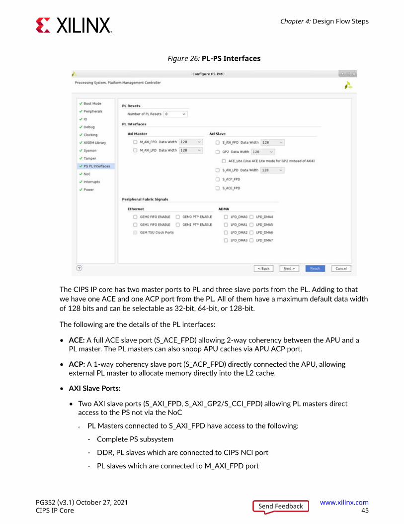
Figure 26: PL-PS Interfaces
The CIPS IP core has two master ports to PL and three slave ports from the PL. Adding to thatwe have one ACE and one ACP port from the PL. All of them have a maximum default data widthof 128 bits and can be selectable as 32-bit, 64-bit, or 128-bit.
The following are the details of the PL interfaces:
• ACE: A full ACE slave port (S_ACE_FPD) allowing 2-way coherency between the APU and aPL master. The PL masters can also snoop APU caches via APU ACP port.
• ACP: A 1-way coherency slave port (S_ACP_FPD) directly connected the APU, allowingexternal PL master to allocate memory directly into the L2 cache.
• AXI Slave Ports:
• Two AXI slave ports (S_AXI_FPD, S_AXI_GP2/S_CCI_FPD) allowing PL masters directaccess to the PS not via the NoC
○ PL Masters connected to S_AXI_FPD have access to the following:
- Complete PS subsystem
- DDR, PL slaves which are connected to CIPS NCI port
- PL slaves which are connected to M_AXI_FPD port
Chapter 4: Design Flow Steps
PG352 (v3.1) October 27, 2021 www.xilinx.comCIPS IP Core 45Send Feedback

○ PL Masters connected to GP2 port have access to the following:
- Complete PS subsystem
- DDR, PL slaves which are connected to CIPS CCI port
- PL slaves which are connected to M_AXI_FPD port
• One direct AXI slave port ( S_AXI_LPD) allowing PL masters access to LPD independent ofFPD power state. PL masters connected to this masters has access to complete LPDsubsystem.
Note: The GP2 port can be used as either an AXI4 port or as an ACE_Lite port. To enable ACE_Litemode, enable the GP2 port in the GUI and select the ACE_Lite mode.
• AXI Mater Ports:
• One AXI master port (M_AXI_FPD) allowing PS masters and PL masters (which areconnected to CIPS S_AXI_FPD, GP2 and CIPS NOC slave ports) access to PL slaves.
• One direct AXI master port (M_AXI_LPD) allowing LPD masters access to PL slavesindependent of FPD power state.
The Versal CIPS IP core provides four resets to the PL. It enables the configuration of theseresets to be used in the PL, which are asynchronous to any clock. These resets will be de-asserted after the PL configuration process.
Using this page, you can also configure the PS to PL interface signals related to Ethernet (FIFO,PTP and TSU) and LPD_DMA flow control support.
Masters have to choose different addresses for the connected PL slaves. Based on which AXIport the slaves are connected to CIPS, following table shows the possible addresses for PL slaves.
Table 6: AXI Region Addresses
Interface Region Start Address SizeM_AXI_LPD LPD_AFI_FS 0x80000000 512 MB
M_AXI_FPD
FPD_AFI_0 0xA4000000 192 MB
FPD_AFI_1 0xB0000000 256 MB
FPD_PL8GB 0x400000000 8 GB
FPD_PL1TB 0x4000000000 1 TB
Programmable Logic InterruptsThe Control Interfaces and Processing System IP core provides three PS to PL interrupt interfaces(in turn these has wide number of shared interrupts for each peripheral) and 16 PL to PSinterrupts. Also, the CIPS IP core has a list of Processor and Debug interrupts.
Chapter 4: Design Flow Steps
PG352 (v3.1) October 27, 2021 www.xilinx.comCIPS IP Core 46Send Feedback

The Interrupt Configuration tab is used to enable/disable the interrupts between the CIPS coreand the PL.
These are broadly categorized as the following:
• PS to PL : We have wide number of shared interrupts from different regions of PS (LPD,FPD,and PMC) to PL masters or slaves. You can enable these interrupts separately for eachdomain and can connect each peripheral interrupt signal to PL logic.
• PL to PS : There are 16 PL to PS interrupts that are supported. These are shared interruptsfrom PL logic to GICs of Real-time Processing Unit (RPU) and Application Processing Unit(APU).
• High priority PL to PS cores (Processor): These are Legacy FIQ/IRQ interrupts for RPU/APUfrom PL. One IRQ and FIQ per CPU will be routed from PL to GIC.
• Inter Processor Interrupt: The Inter Processor Interrupt Block provides the ability for anyprocessing unit to interrupt another processing unit by performing a register write. There areseven IPI channels (IPI 0 through IPI 6), which can be assigned to APU, RPU, and PL.
Figure 27: Interrupt Configuration
The interrupts from the Control, Interfaces and Processing System IP core I/O peripherals (IOP)are routed to the PL. The PL can asynchronously assert up to 20 interrupts to the PS cores likeAPU/RPU.
Chapter 4: Design Flow Steps
PG352 (v3.1) October 27, 2021 www.xilinx.comCIPS IP Core 47Send Feedback

• 16 interrupt signals are mapped to the interrupt controller as a peripheral interrupt whereeach interrupt signal is set to a priority level and mapped to one or both CPUs. To use morethan one interrupt signal, use a Concat block in the Vivado IP integrator to automatically sizethe width of the interrupt vector.
• The remaining four PL interrupt signals are inverted and routed to the nFIQ and nIRQinterrupt directly to the signals to the private peripheral interrupt (PPI) unit of the interruptcontroller. There is an nFIQ and nIRQ interrupt for each of two CPUs.
The Interrupt IDs are exported to SW and the same ID can be seen in xparameters.h file orsee the Versal ACAP Technical Reference Manual (AM011).
Power ConfigurationThis page enables you to select the Low Voltage Complementary Metal Oxide Semiconductor(LVCMOS) for Banks. Each bank has a common I/O Voltage Standard for all corresponding MIOs.The default value is LVCMOS1.8 and two more options of LVCMOS2.5 and LVCMOS3.3 I/Ovoltage standard.
This setting must reflect the board LVCMOS voltage used per MIO bank. These settings are notused to set up any register or the MIO voltage. They are used by Vivado report_power toestimate power consumption.
Chapter 4: Design Flow Steps
PG352 (v3.1) October 27, 2021 www.xilinx.comCIPS IP Core 48Send Feedback

Figure 28: MIO Voltage Standard
Debug SettingsFor information on debugging, see Vivado Design Suite User Guide: Programming and Debugging(UG908).
PS-PL Cross TriggerThe PL to PS Cross Trigger inputs are trigger inputs from PL. You can enable these ports to getthe trigger events from hardware and feed to ILA for analyzing/debugging hardware state.
The PS to PL Cross Trigger outputs can be used to set the debug break points in software to haltthe hardware. Once the trigger event is given to the hardware, the software accesses thehardware state for debug.
Chapter 4: Design Flow Steps
PG352 (v3.1) October 27, 2021 www.xilinx.comCIPS IP Core 49Send Feedback
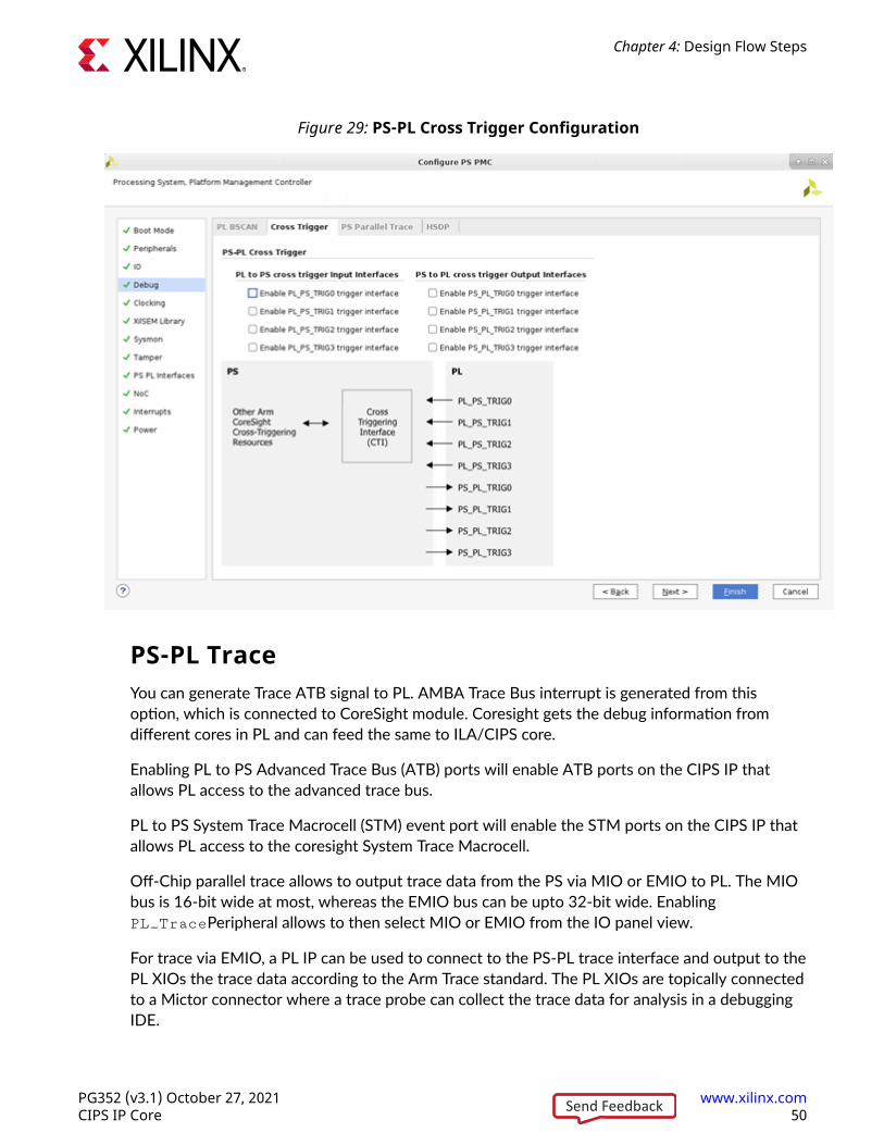
Figure 29: PS-PL Cross Trigger Configuration
PS-PL TraceYou can generate Trace ATB signal to PL. AMBA Trace Bus interrupt is generated from thisoption, which is connected to CoreSight module. Coresight gets the debug information fromdifferent cores in PL and can feed the same to ILA/CIPS core.
Enabling PL to PS Advanced Trace Bus (ATB) ports will enable ATB ports on the CIPS IP thatallows PL access to the advanced trace bus.
PL to PS System Trace Macrocell (STM) event port will enable the STM ports on the CIPS IP thatallows PL access to the coresight System Trace Macrocell.
Off-Chip parallel trace allows to output trace data from the PS via MIO or EMIO to PL. The MIObus is 16-bit wide at most, whereas the EMIO bus can be upto 32-bit wide. EnablingPL_TracePeripheral allows to then select MIO or EMIO from the IO panel view.
For trace via EMIO, a PL IP can be used to connect to the PS-PL trace interface and output to thePL XIOs the trace data according to the Arm Trace standard. The PL XIOs are topically connectedto a Mictor connector where a trace probe can collect the trace data for analysis in a debuggingIDE.
Chapter 4: Design Flow Steps
PG352 (v3.1) October 27, 2021 www.xilinx.comCIPS IP Core 50Send Feedback
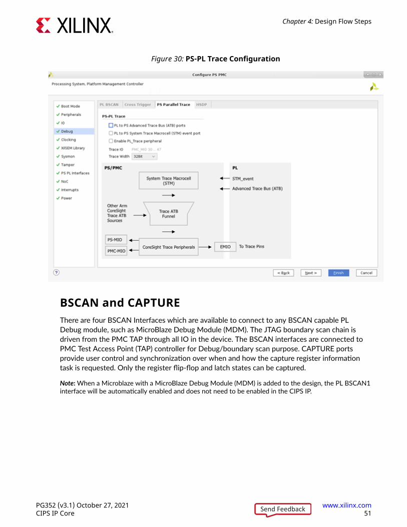
Figure 30: PS-PL Trace Configuration
BSCAN and CAPTUREThere are four BSCAN Interfaces which are available to connect to any BSCAN capable PLDebug module, such as MicroBlaze Debug Module (MDM). The JTAG boundary scan chain isdriven from the PMC TAP through all IO in the device. The BSCAN interfaces are connected toPMC Test Access Point (TAP) controller for Debug/boundary scan purpose. CAPTURE portsprovide user control and synchronization over when and how the capture register informationtask is requested. Only the register flip-flop and latch states can be captured.
Note: When a Microblaze with a MicroBlaze Debug Module (MDM) is added to the design, the PL BSCAN1interface will be automatically enabled and does not need to be enabled in the CIPS IP.
Chapter 4: Design Flow Steps
PG352 (v3.1) October 27, 2021 www.xilinx.comCIPS IP Core 51Send Feedback

Figure 31: BSCAN and CAPTURE Configuration
High-Speed Debug Port (HSDP)High-Speed Debug Port is a protocol that provides debug and trace for the programmable logic(PL), processing system (PS) and the AI Engines. HSDP can use gigabit transceivers on the deviceto provide better performance than the JTAG interface.
As HSDP is a protocol, the transaction layer is handled by the Debug Packet Controller (DPC) andthe link layer can be one of the four interfaces listed below:
• JTAG
• HSDP Aurora (hardened Aurora IP)
• CPM PCIe Controller
• PL Aurora (soft Aurora IP)
Chapter 4: Design Flow Steps
PG352 (v3.1) October 27, 2021 www.xilinx.comCIPS IP Core 52Send Feedback

WARNING! Be very careful when using the hardened HSDP Aurora as this can impose limitations on theGTY transceivers available to the rest of the design. For more information on the limitations, see XPIPEGTY Transceiver Channels table in Versal ACAP Technical Reference Manual (AM011). For moreinformation on high-speed debug port see Integrated Debug chapter in Versal ACAP Technical ReferenceManual (AM011).
Figure 32: High Speed Debug Port
Boot ModeVersal® device boots differently from traditional FPGAs. There is no longer a standalonebitstream, but instead in Versal device has a programmable device image (PDI) that includes a PLConfiguration Frame Data. The Configuration Frame Interface (CFI) is the interface used toconfigure the Configuration Frames with the Configuration Frame Data. The CFI belongs in thePMC. The PMC BootROM is responsible to read the PLM from the PDI via the boot mediumselected.
Chapter 4: Design Flow Steps
PG352 (v3.1) October 27, 2021 www.xilinx.comCIPS IP Core 53Send Feedback

The PLM includes boot device configuration. Select the boot devices in the Boot Mode page.Multiple boot devices can be selected as supported on the board. Clock settings such as requiredfrequency for boot peripherals and REF_CLK frequency can be set in this page. If you want touse only the PL section, you should use this page to configure boot peripherals.
QSPI, OSPI, SD0, SD1, eMMC1, and SelectMAP are all primary boot peripheral options. The SD0,SD1, and eMMC1 settings provide flags if the MIO selected is not supported for primary boot.An information message is shown in Vivado GUI for SD0/1 on usage as Storage or Boot (and/or)Storage.
STARTUP options are available to interface device pins and logic to the global asynchronous set/reset signal, the global 3-state dedicated routing, and the end of startup (EOS).
The STARTUP options supported in Tcl command prompt, you can setCONFIG.PS_PMC_CONFIG to one to get this primitive ports on CIPS.
set_property CONFIG.PS_PMC_CONFIG {PS_USE_STARTUP 1 } [get_bd_cells /versal_cips_0]
Figure 33: Boot Mode Configuration
Note: For more information on the Versal ACAP Technical Reference Manual (AM011) and Versal ACAPSystem Software Developers Guide (UG1304).
Chapter 4: Design Flow Steps
PG352 (v3.1) October 27, 2021 www.xilinx.comCIPS IP Core 54Send Feedback
Appendix A
UpgradingFor upgrade support from previous version(s), see AR76535.
Appendix A: Upgrading
PG352 (v3.1) October 27, 2021 www.xilinx.comCIPS IP Core 55Send Feedback

Appendix B
DebuggingThis appendix includes details about resources available on the Xilinx® Support website anddebugging tools.
If the IP requires a license key, the key must be verified. The Vivado® design tools have severallicense checkpoints for gating licensed IP through the flow. If the license check succeeds, the IPcan continue generation. Otherwise, generation halts with an error. License checkpoints areenforced by the following tools:
• Vivado Synthesis
• Vivado Implementation
• write_bitstream (Tcl command)
IMPORTANT! IP license level is ignored at checkpoints. The test confirms a valid license exists. It does notcheck IP license level.
Finding Help on Xilinx.comTo help in the design and debug process when using the core, the Xilinx Support web pagecontains key resources such as product documentation, release notes, answer records,information about known issues, and links for obtaining further product support. The XilinxCommunity Forums are also available where members can learn, participate, share, and askquestions about Xilinx solutions.
DocumentationThis product guide is the main document associated with the core. This guide, along withdocumentation related to all products that aid in the design process, can be found on the XilinxSupport web page or by using the Xilinx® Documentation Navigator. Download the XilinxDocumentation Navigator from the Downloads page. For more information about this tool andthe features available, open the online help after installation.
Appendix B: Debugging
PG352 (v3.1) October 27, 2021 www.xilinx.comCIPS IP Core 56Send Feedback

Answer RecordsAnswer Records include information about commonly encountered problems, helpful informationon how to resolve these problems, and any known issues with a Xilinx product. Answer Recordsare created and maintained daily ensuring that users have access to the most accurateinformation available.
Answer Records for this core can be located by using the Search Support box on the main Xilinxsupport web page. To maximize your search results, use keywords such as:
• Product name
• Tool message(s)
• Summary of the issue encountered
A filter search is available after results are returned to further target the results.
Technical SupportXilinx provides technical support on the Xilinx Community Forums for this LogiCORE™ IP productwhen used as described in the product documentation. Xilinx cannot guarantee timing,functionality, or support if you do any of the following:
• Implement the solution in devices that are not defined in the documentation.
• Customize the solution beyond that allowed in the product documentation.
• Change any section of the design labeled DO NOT MODIFY.
To ask questions, navigate to the Xilinx Community Forums.
Debug ToolsThere are many tools available to address CIPS design issues. It is important to know which toolsare useful for debugging various situations.
Vivado Design Suite Debug FeatureThe Vivado® Design Suite debug feature inserts logic analyzer and virtual I/O cores directly intoyour design. The debug feature also allows you to set trigger conditions to capture applicationand integrated block port signals in hardware. Captured signals can then be analyzed. Thisfeature in the Vivado IDE is used for logic debugging and validation of a design running in Xilinx®
devices.
Appendix B: Debugging
PG352 (v3.1) October 27, 2021 www.xilinx.comCIPS IP Core 57Send Feedback

The Vivado logic analyzer is used to interact with the logic debug LogiCORE IP cores, including:
• ILA 2.0 (and later versions)
• VIO 2.0 (and later versions)
See the Vivado Design Suite User Guide: Programming and Debugging (UG908).
Appendix B: Debugging
PG352 (v3.1) October 27, 2021 www.xilinx.comCIPS IP Core 58Send Feedback

Appendix C
Additional Resources and LegalNotices
Xilinx ResourcesFor support resources such as Answers, Documentation, Downloads, and Forums, see XilinxSupport.
Documentation Navigator and Design HubsXilinx® Documentation Navigator (DocNav) provides access to Xilinx documents, videos, andsupport resources, which you can filter and search to find information. To open DocNav:
• From the Vivado® IDE, select Help → Documentation and Tutorials.
• On Windows, select Start → All Programs → Xilinx Design Tools → DocNav.
• At the Linux command prompt, enter docnav.
Xilinx Design Hubs provide links to documentation organized by design tasks and other topics,which you can use to learn key concepts and address frequently asked questions. To access theDesign Hubs:
• In DocNav, click the Design Hubs View tab.
• On the Xilinx website, see the Design Hubs page.
Note: For more information on DocNav, see the Documentation Navigator page on the Xilinx website.
ReferencesThese documents provide supplemental material useful with this guide:
Appendix C: Additional Resources and Legal Notices
PG352 (v3.1) October 27, 2021 www.xilinx.comCIPS IP Core 59Send Feedback

1. OS and Libraries Document Collection (UG643)
2. Vivado Design Suite User Guide: Designing with IP (UG896)
3. Vivado Design Suite User Guide: Logic Simulation (UG900)
4. Vivado Design Suite User Guide: Getting Started (UG910)
5. Vivado Design Suite User Guide: Designing IP Subsystems using IP Integrator (UG994)
6. Vivado Design Suite User Guide: Programming and Debugging (UG908)
7. Versal ACAP System Software Developers Guide (UG1304)
8. Versal ACAP System Monitor Architecture Manual (AM006)
9. Versal ACAP Technical Reference Manual (AM011)
10. Versal ACAP Register Reference (AM012)
11. Versal ACAP CPM CCIX Architecture Manual (AM016)
12. Versal ACAP CPM Mode for PCI Express Product Guide (PG346)
13. Versal ACAP CPM DMA and Bridge Mode for PCI Express Product Guide (PG347)
14. Versal ACAP Programmable Network on Chip and Integrated Memory Controller LogiCORE IPProduct Guide (PG313)
Revision HistoryThe following table shows the revision history for this document.
Section Revision Summary10/27/2021 Version 3.1
Chapter 4: Design Flow Steps Updated screens for CIPS 3.1.
Output Clocks Added LPD Top switch clocking restriction.
AXI4 I/O Compliant Interfaces Added ACE-Lite GUI information.
Boot Mode • Added CONFIG.PS_PMC_CONFIG parameter.
• Deleted CONFIG.PS_USE_STARTUP parameter.
Appendix A: Upgrading Added appendix.
06/16/2021 Version 3.0
Chapter 4: Design Flow Steps • Updated screens from CIPS 3.0.• Added Choosing a Design Flow, CIPS Presets, and Power
Configuration sections.• Added support of CPM5.
Automation • Modified Board automation through Block automation.• Added support of LPDDR in Block Automation.
Tamper Events/Response Configuration Deleted Voltage Tamper event.
Appendix C: Additional Resources and Legal Notices
PG352 (v3.1) October 27, 2021 www.xilinx.comCIPS IP Core 60Send Feedback

Section Revision SummaryXilSEM Library Configuration Modified content for detect and correct soft errors.
12/04/2020 Version 2.1
Initial release. N/A
Please Read: Important Legal NoticesThe information disclosed to you hereunder (the "Materials") is provided solely for the selectionand use of Xilinx products. To the maximum extent permitted by applicable law: (1) Materials aremade available "AS IS" and with all faults, Xilinx hereby DISCLAIMS ALL WARRANTIES ANDCONDITIONS, EXPRESS, IMPLIED, OR STATUTORY, INCLUDING BUT NOT LIMITED TOWARRANTIES OF MERCHANTABILITY, NON-INFRINGEMENT, OR FITNESS FOR ANYPARTICULAR PURPOSE; and (2) Xilinx shall not be liable (whether in contract or tort, includingnegligence, or under any other theory of liability) for any loss or damage of any kind or naturerelated to, arising under, or in connection with, the Materials (including your use of theMaterials), including for any direct, indirect, special, incidental, or consequential loss or damage(including loss of data, profits, goodwill, or any type of loss or damage suffered as a result of anyaction brought by a third party) even if such damage or loss was reasonably foreseeable or Xilinxhad been advised of the possibility of the same. Xilinx assumes no obligation to correct anyerrors contained in the Materials or to notify you of updates to the Materials or to productspecifications. You may not reproduce, modify, distribute, or publicly display the Materialswithout prior written consent. Certain products are subject to the terms and conditions ofXilinx's limited warranty, please refer to Xilinx's Terms of Sale which can be viewed at https://www.xilinx.com/legal.htm#tos; IP cores may be subject to warranty and support terms containedin a license issued to you by Xilinx. Xilinx products are not designed or intended to be fail-safe orfor use in any application requiring fail-safe performance; you assume sole risk and liability foruse of Xilinx products in such critical applications, please refer to Xilinx's Terms of Sale which canbe viewed at https://www.xilinx.com/legal.htm#tos.
AUTOMOTIVE APPLICATIONS DISCLAIMER
AUTOMOTIVE PRODUCTS (IDENTIFIED AS "XA" IN THE PART NUMBER) ARE NOTWARRANTED FOR USE IN THE DEPLOYMENT OF AIRBAGS OR FOR USE IN APPLICATIONSTHAT AFFECT CONTROL OF A VEHICLE ("SAFETY APPLICATION") UNLESS THERE IS ASAFETY CONCEPT OR REDUNDANCY FEATURE CONSISTENT WITH THE ISO 26262AUTOMOTIVE SAFETY STANDARD ("SAFETY DESIGN"). CUSTOMER SHALL, PRIOR TO USINGOR DISTRIBUTING ANY SYSTEMS THAT INCORPORATE PRODUCTS, THOROUGHLY TESTSUCH SYSTEMS FOR SAFETY PURPOSES. USE OF PRODUCTS IN A SAFETY APPLICATIONWITHOUT A SAFETY DESIGN IS FULLY AT THE RISK OF CUSTOMER, SUBJECT ONLY TOAPPLICABLE LAWS AND REGULATIONS GOVERNING LIMITATIONS ON PRODUCTLIABILITY.
Appendix C: Additional Resources and Legal Notices
PG352 (v3.1) October 27, 2021 www.xilinx.comCIPS IP Core 61Send Feedback

Copyright
© Copyright 2020-2021 Xilinx, Inc. Xilinx, the Xilinx logo, Alveo, Artix, Kintex, Kria, Spartan,Versal, Vitis, Virtex, Vivado, Zynq, and other designated brands included herein are trademarks ofXilinx in the United States and other countries. AMBA, AMBA Designer, Arm, ARM1176JZ-S,CoreSight, Cortex, PrimeCell, Mali, and MPCore are trademarks of Arm Limited in the EU andother countries. PCI, PCIe, and PCI Express are trademarks of PCI-SIG and used under license. Allother trademarks are the property of their respective owners.
Appendix C: Additional Resources and Legal Notices
PG352 (v3.1) October 27, 2021 www.xilinx.comCIPS IP Core 62Send Feedback