Embed Size (px)
Citation preview
Contributions to the Evaluation of Ensembles of Combinational Logic Gates
R. P. R. P. RibasRibas, S. Bavaresco, N. Schuch, V. Callegaro, M. Lubaszewski, A. I. Reis
Institute of Informatics Institute of Informatics –– UFRGS, Brazil.UFRGS, Brazil.
ISCAS 2009 & Microelectronics Journal (Jan.2011)ISCAS 2009 & Microelectronics Journal (Jan.2011)

OUTLINEOUTLINE
• Introduction and motivation
• Goals of this work (design specification)
• Design of combinational blocks (key point)
• Circuit architecture and operation modes
• Conclusions and future works
2

3
• ASIC design: standard cellsstandard cells flow (based on cell libraries).
• Pre-designed cell librarieslibraries include in majority combinational
gates of different logic functionslogic functions and with different drive drive
strengthstrength options.
• Handcrafted gate design: prepre--defined librarydefined library composition.
•• Automatic generated cellsAutomatic generated cells (“liquid or soft cells”): library-free
technology mapping concept (promising possibility for “in-
place optimization” - IPO).
• “Liquid cells” (generated by software) must also be prepre--
characterizedcharacterized for using in IC design flow.
INTRODUCTIONINTRODUCTION
4
• On silicon standard cell library validationlibrary validation: for each new
process and library composition.
• Specific test structurestest structures: ring oscillators, mixed cell chains,
counters, ….
•• TapeTape--outsouts of benchmarks and application circuits.
•• Full library verificationFull library verification: functionality and performance.
•• Library providerLibrary provider: test engineering cost, use of ATE, time-to-
market, quality, confiability, responsibility and certification, …
INTRODUCTIONINTRODUCTION
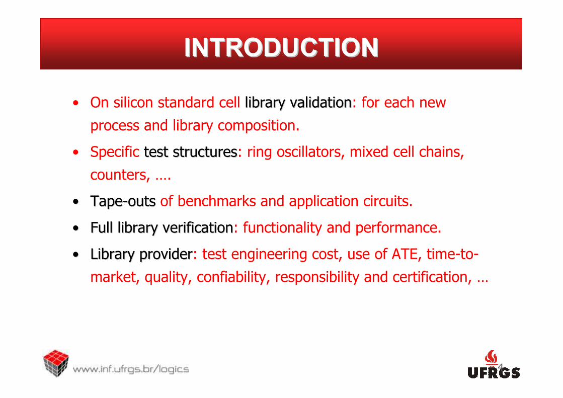
• Automatic generation provides fast and huge librarieshuge libraries.
•• SpecificSpecific test structurestest structures require handcraft design (design
time and costs proportional to the library composition).
• Ring oscillators and isolated cells under test
5
ringring oscillatorsoscillators
MOTIVATIONMOTIVATION
En
Vdd Vdd VddVdd
. . .. . .
. . .
isolatedisolated cellscells underunder testtest
tc t_outputt_input

•• Benchmark circuitsBenchmark circuits are not effective for fully functional
library verification and validation.
6
4328,089wb_conmax_top
64645,5945,594tv80_coretv80_core
586,245mc_top
439,203iu
42679i2c_master_top
411,311c7552
# different cells# cells in the circuitISCAS Benchmarks
Small Small librarylibrary withwith 64 64 combinationalcombinational cellscells
MOTIVATIONMOTIVATION
• There is no guarantee about complete functional stimulicomplete functional stimuli
of each different library cell instantiated.
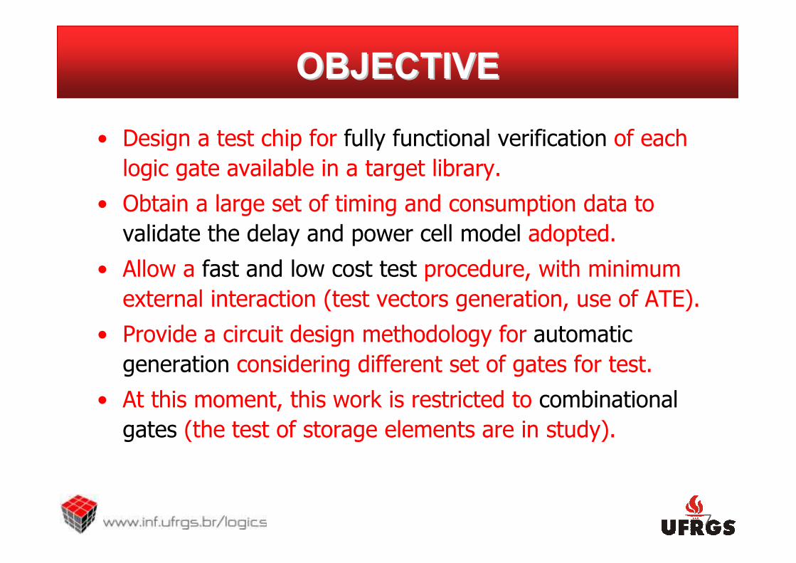
• Design a test chip for fully functional verification of each
logic gate available in a target library.
• Obtain a large set of timing and consumption data to
validate the delay and power cell model adopted.
• Allow a fast and low cost test procedure, with minimum
external interaction (test vectors generation, use of ATE).
• Provide a circuit design methodology for automatic
generation considering different set of gates for test.
• At this moment, this work is restricted to combinational
gates (the test of storage elements are in study).
7
OBJECTIVEOBJECTIVE

OUTLINEOUTLINE
• Introduction and motivation
• Goals of this work (design specification)
• Design of combinational blocks (key point)
• Circuit architecture and operation modes
• Conclusions and future works
8

9
COMBINATIONAL BLOCKSCOMBINATIONAL BLOCKS
Two stages can be identified:
•• FirstFirst: composed by a minimum number of different library
cells, directly connected to block inputs (one-level depth).
•• SecondSecond: circuit used to recreate the original combinational
block input at the block output (multi-level circuit).
n-outputsn-inputs
W1
W2
W3
Wm
C1
C2
Cm
C3
10
COMBINATIONAL BLOCKSCOMBINATIONAL BLOCKS
n-outputsn-inputs
W1
W2
W3
Wm
C1
C2
Cm
C3
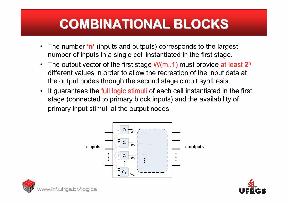
• The number ‘‘nn’’ (inputs and outputs) corresponds to the largest
number of inputs in a single cell instantiated in the first stage.
• The output vector of the first stage W(m..1)W(m..1) must provide at leastat least 22nn
different values in order to allow the recreation of the input data at
the output nodes through the second stage circuit synthesis.
• It guarantees the full logic stimulifull logic stimuli of each cell instantiated in the first
stage (connected to primary block inputs) and the availability of
primary input stimuli at the output nodes.
11
COMBINATIONAL BLOCKSCOMBINATIONAL BLOCKS
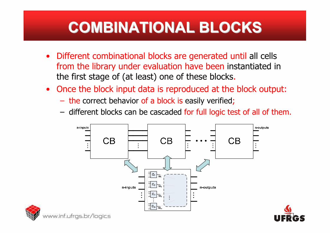
• Different combinational blocks are generated until all cellsfrom the library under evaluation have been instantiated in the first stage of (at least) one of these blocks.
• Once the block input data is reproduced at the block output:
– the correct behavior of a block is easily verified;
– different blocks can be cascaded for full logic test of all of them.
12
COMBINATIONAL BLOCKS GENERATIONCOMBINATIONAL BLOCKS GENERATION
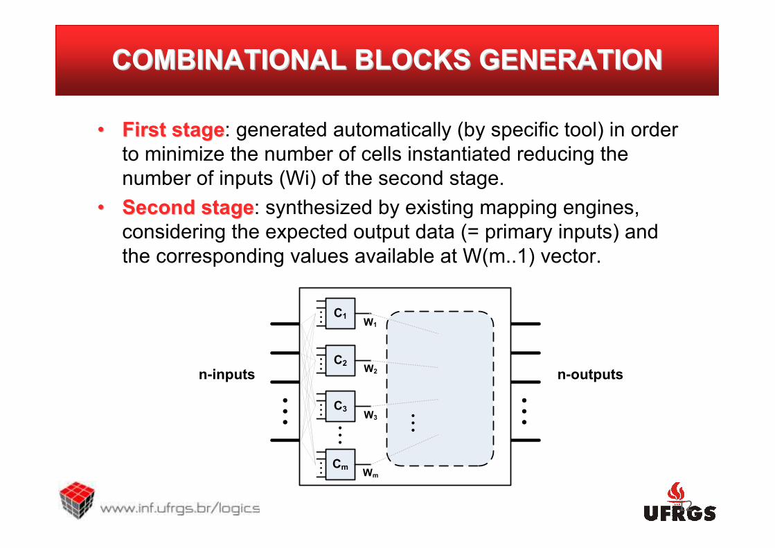
•• First stageFirst stage: generated automatically (by specific tool) in order
to minimize the number of cells instantiated reducing the
number of inputs (Wi) of the second stage.
•• Second stageSecond stage: synthesized by existing mapping engines,
considering the expected output data (= primary inputs) and
the corresponding values available at W(m..1) vector.
n-outputsn-inputs
W1
W2
W3
Wm
C1
C2
Cm
C3
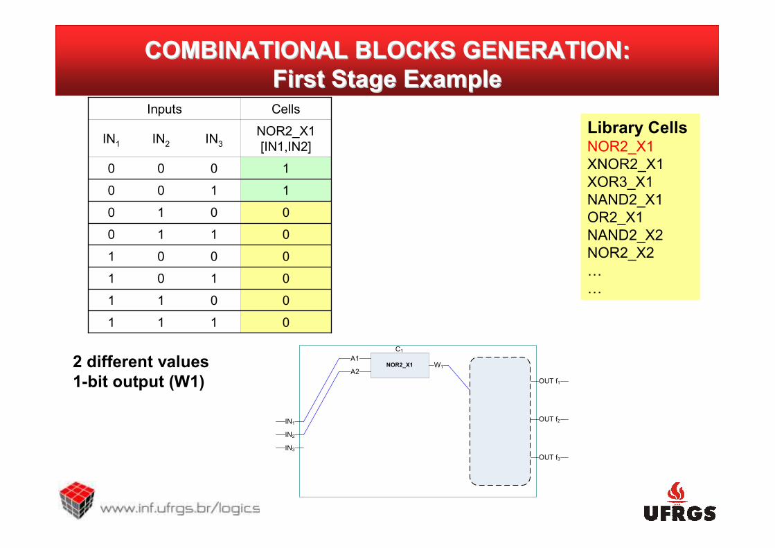
0111
0011
0101
0001
0110
0010
1100
1000
NOR2_X1
[IN1,IN2]IN3IN2IN1
CellsInputs
2 different values
1-bit output (W1)
NOR2_X1
A2
A1
IN1
IN2
IN3
W1
OUT f1
OUT f2
OUT f3
C1
Library CellsNOR2_X1
XNOR2_X1
XOR3_X1
NAND2_X1
OR2_X1
NAND2_X2
NOR2_X2
…
…
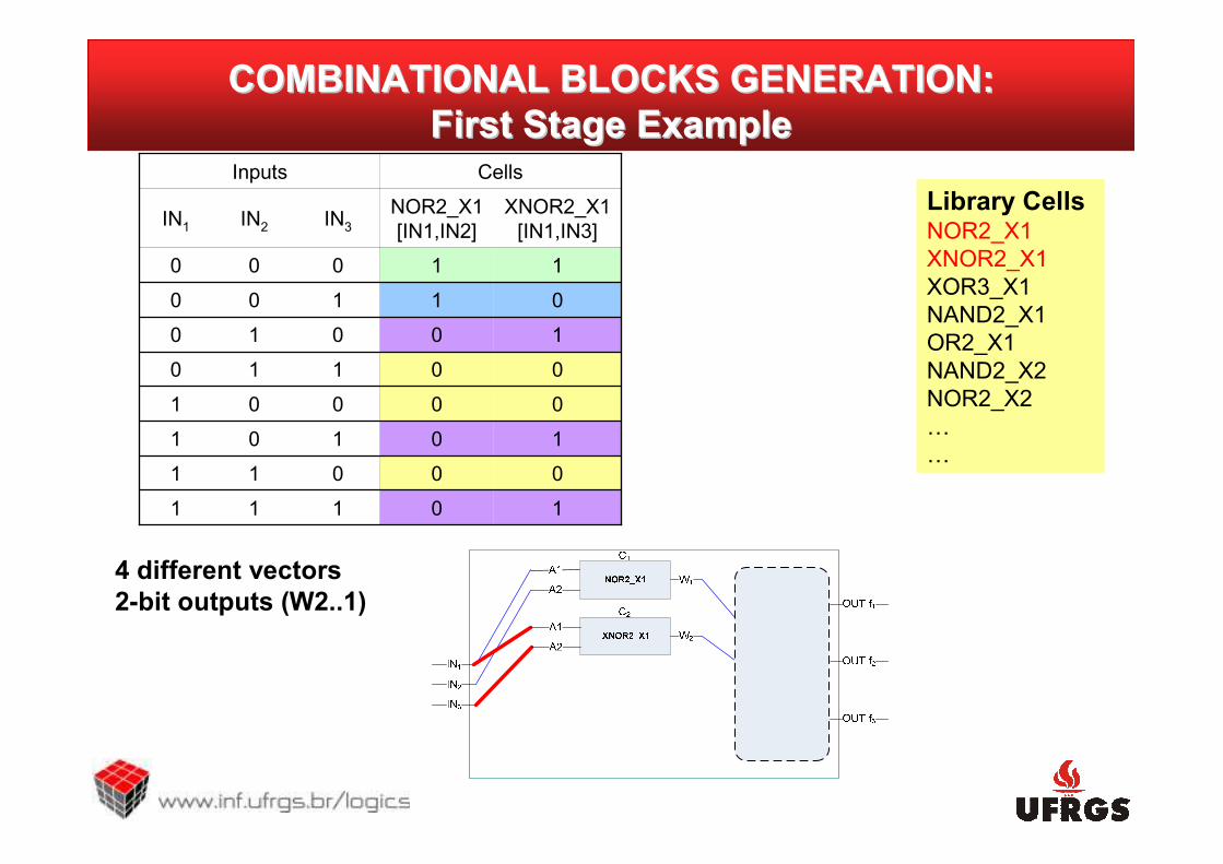
COMBINATIONAL BLOCKS GENERATION:COMBINATIONAL BLOCKS GENERATION:
First Stage ExampleFirst Stage Example
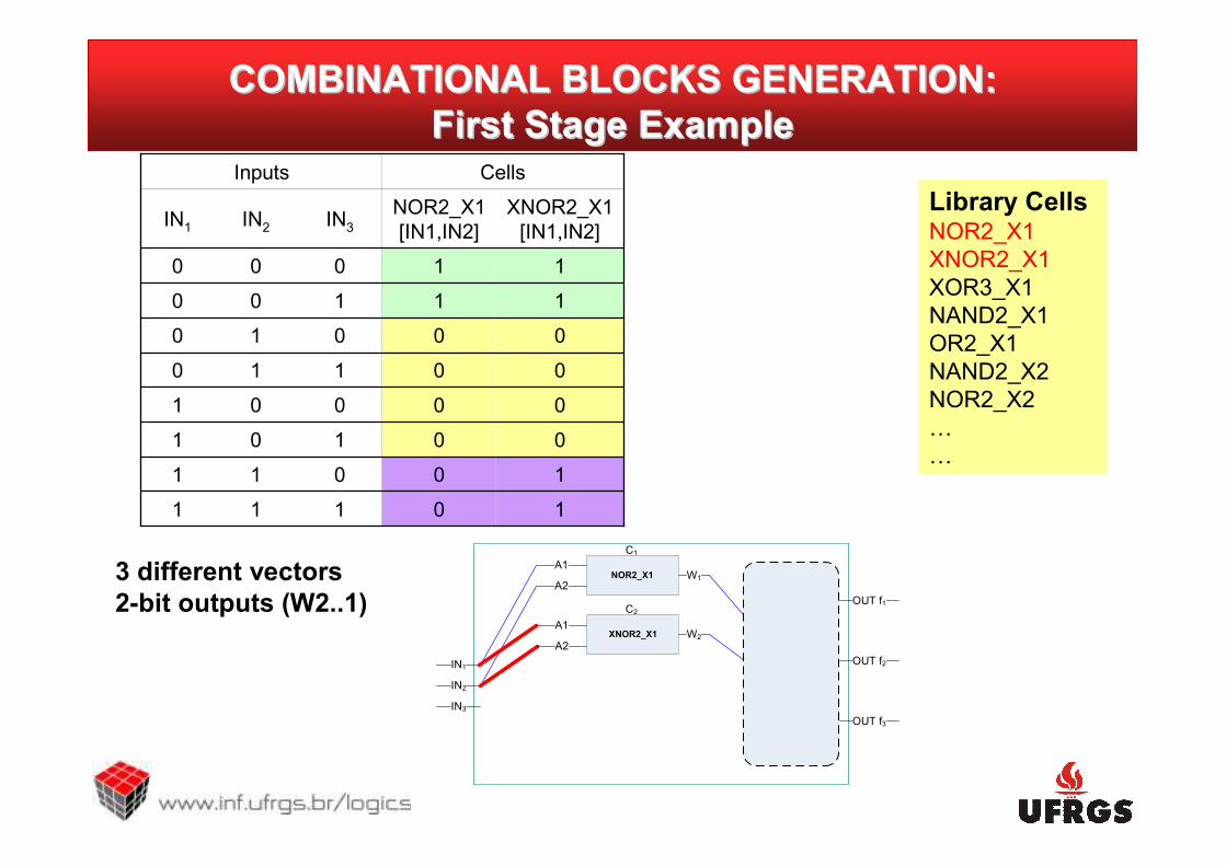
3 different vectors
2-bit outputs (W2..1)
10111
10011
00101
00001
00110
00010
11100
11000
XNOR2_X1
[IN1,IN2]
NOR2_X1
[IN1,IN2]IN3IN2IN1
CellsInputs
Library CellsNOR2_X1
XNOR2_X1
XOR3_X1
NAND2_X1
OR2_X1
NAND2_X2
NOR2_X2
…
…
NOR2_X1
A2
A1
IN1
IN2
IN3
W1
W2
OUT f1
OUT f2
OUT f3
A2
A1
C1
C2
XNOR2_X1
COMBINATIONAL BLOCKS GENERATION:COMBINATIONAL BLOCKS GENERATION:
First Stage ExampleFirst Stage Example
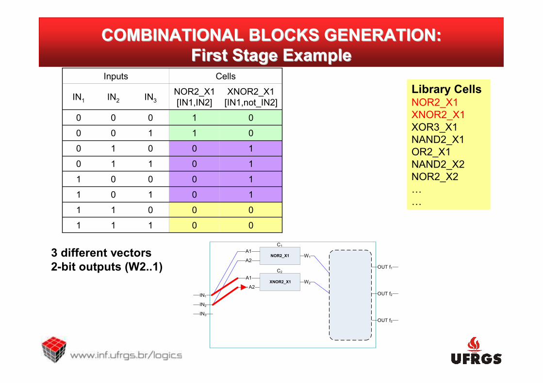
00111
00011
10101
10001
10110
10010
01100
01000
XNOR2_X1
[IN1,not_IN2]
NOR2_X1
[IN1,IN2]IN3IN2IN1
CellsInputs
Library CellsNOR2_X1
XNOR2_X1
XOR3_X1
NAND2_X1
OR2_X1
NAND2_X2
NOR2_X2
…
…
NOR2_X1
A2
A1
IN1
IN2
IN3
W1
W2
OUT f1
OUT f2
OUT f3
A1
C1
C2
XNOR2_X1
A2
3 different vectors
2-bit outputs (W2..1)
COMBINATIONAL BLOCKS GENERATION:COMBINATIONAL BLOCKS GENERATION:
First Stage ExampleFirst Stage Example

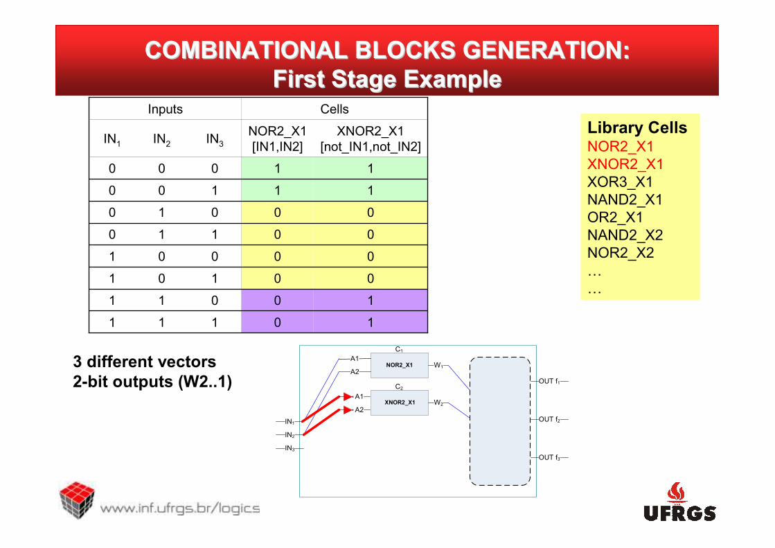
00111
00011
10101
10001
10110
10010
01100
01000
XNOR2_X1
[not_IN1,IN2]
NOR2_X1
[IN1,IN2]IN3IN2IN1
CellsInputs
Library CellsNOR2_X1
XNOR2_X1
XOR3_X1
NAND2_X1
OR2_X1
NAND2_X2
NOR2_X2
…
…
3 different vectors
2-bit outputs (W2..1)
COMBINATIONAL BLOCKS GENERATION:COMBINATIONAL BLOCKS GENERATION:
First Stage ExampleFirst Stage Example
10111
10011
00101
00001
00110
00010
11100
11000
XNOR2_X1
[not_IN1,not_IN2]
NOR2_X1
[IN1,IN2]IN3IN2IN1
CellsInputs
Library CellsNOR2_X1
XNOR2_X1
XOR3_X1
NAND2_X1
OR2_X1
NAND2_X2
NOR2_X2
…
…
NOR2_X1
A2
A1
IN1
IN2
IN3
W1
W2
OUT f1
OUT f2
OUT f3
C1
C2
XNOR2_X1A1
A2
3 different vectors
2-bit outputs (W2..1)
COMBINATIONAL BLOCKS GENERATION:COMBINATIONAL BLOCKS GENERATION:
First Stage ExampleFirst Stage Example

10111
10011
00101
00001
00110
00010
11100
11000
XNOR2_X1
[IN2,IN1]
NOR2_X1
[IN1,IN2]IN3IN2IN1
CellsInputs
Library CellsNOR2_X1
XNOR2_X1
XOR3_X1
NAND2_X1
OR2_X1
NAND2_X2
NOR2_X2
…
…
3 different vectors
2-bit outputs (W2..1)
COMBINATIONAL BLOCKS GENERATION:COMBINATIONAL BLOCKS GENERATION:
First Stage ExampleFirst Stage Example

00111
00011
10101
10001
10110
10010
01100
01000
XNOR2_X1
[IN2,not_IN1]
NOR2_X1
[IN1,IN2]IN3IN2IN1
CellsInputs
Library CellsNOR2_X1
XNOR2_X1
XOR3_X1
NAND2_X1
OR2_X1
NAND2_X2
NOR2_X2
…
…
NOR2_X1
A2
A1
IN1
IN2
IN3
W1
W2
OUT f1
OUT f2
OUT f3
A1
C1
C2
XNOR2_X1
A2
3 different vectors
2-bit outputs (W2..1)
COMBINATIONAL BLOCKS GENERATION:COMBINATIONAL BLOCKS GENERATION:
First Stage ExampleFirst Stage Example

00111
00011
10101
10001
10110
10010
01100
01000
XNOR2_X1
[not_IN2,IN1]
NOR2_X1
[IN1,IN2]IN3IN2IN1
CellsInputs
Library CellsNOR2_X1
XNOR2_X1
XOR3_X1
NAND2_X1
OR2_X1
NAND2_X2
NOR2_X2
…
…
NOR2_X1
A2
A1
IN1
IN2
IN3
W1
W2
OUT f1
OUT f2
OUT f3
A2
C1
C2
XNOR2_X1A1
3 different vectors
2-bit outputs (W2..1)
COMBINATIONAL BLOCKS GENERATION:COMBINATIONAL BLOCKS GENERATION:
First Stage ExampleFirst Stage Example

10111
10011
00101
00001
00110
00010
11100
11000
XNOR2_X1
[not_IN2,not_IN1]
NOR2_X1
[IN1,IN2]IN3IN2IN1
CellsInputs
Library CellsNOR2_X1
XNOR2_X1
XOR3_X1
NAND2_X1
OR2_X1
NAND2_X2
NOR2_X2
…
…
3 different vectors
2-bit outputs (W2..1)
COMBINATIONAL BLOCKS GENERATION:COMBINATIONAL BLOCKS GENERATION:
First Stage ExampleFirst Stage Example
10111
00011
10101
00001
00110
10010
01100
11000
XNOR2_X1
[IN1,IN3]
NOR2_X1
[IN1,IN2]IN3IN2IN1
CellsInputs
Library CellsNOR2_X1
XNOR2_X1
XOR3_X1
NAND2_X1
OR2_X1
NAND2_X2
NOR2_X2
…
…
4 different vectors
2-bit outputs (W2..1)
COMBINATIONAL BLOCKS GENERATION:COMBINATIONAL BLOCKS GENERATION:
First Stage ExampleFirst Stage Example
1
0
0
1
0
1
1
0
XOR3_X1
[IN1,IN2,IN3]
10111
00011
10101
00001
00110
10010
01100
11000
XNOR2_X1
[IN1,IN3]
NOR2_X1
[IN1,IN2]IN3IN2IN1
CellsInputs
Library CellsNOR2_X1
XNOR2_X1
XOR3_X1
NAND2_X1
OR2_X1
NAND2_X2
NOR2_X2
…
…
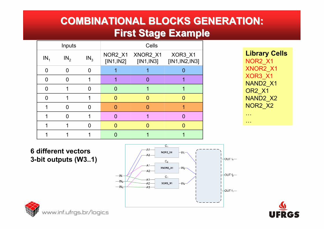
6 different vectors
3-bit outputs (W3..1)
COMBINATIONAL BLOCKS GENERATION:COMBINATIONAL BLOCKS GENERATION:
First Stage ExampleFirst Stage Example
0
0
1
1
1
1
1
1
NAND2_X1
[IN1,IN2]
1
0
0
1
0
1
1
0
XOR3_X1
[IN1,IN2,IN3]
10111
00011
10101
00001
00110
10010
01100
11000
XNOR2_X1
[IN1,IN3]
NOR2_X1
[IN1,IN2]IN3IN2IN1
CellsInputs
NAND2_X1
NOR2_X1
A2
A1
IN1
IN2
IN3
W1
W2
W3
W4
OUT f1
OUT f2
OUT f3
A1
A2
A1
C1
C2
C3
C4
XOR3_X1
XNOR2_X1
A2
A1
A3
A2
Library CellsNOR2_X1
XNOR2_X1
XOR3_X1
NAND2_X1
OR2_X1
NAND2_X2
NOR2_X2
…
…
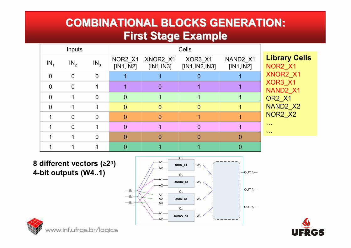
8 different vectors (≥2n)
4-bit outputs (W4..1)
COMBINATIONAL BLOCKS GENERATION:COMBINATIONAL BLOCKS GENERATION:
First Stage ExampleFirst Stage Example
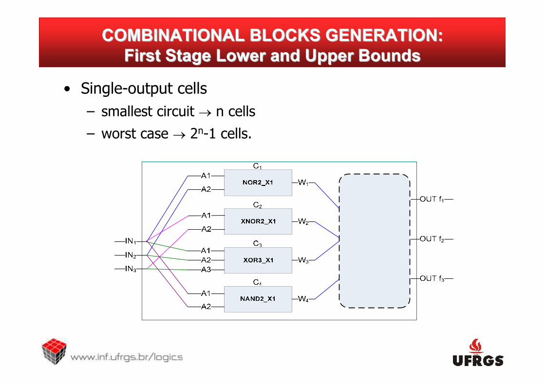
• Single-output cells
– smallest circuit → n cells
– worst case → 2n-1 cells.
COMBINATIONAL BLOCKS GENERATION:COMBINATIONAL BLOCKS GENERATION:
First Stage Lower and Upper BoundsFirst Stage Lower and Upper Bounds
001111
110011
010101
101001
100110
011010
111100
000000
XOR2_X2
(A,C)
XOR2_X1
(B,C)
XOR3_X1
(A,B,C)CBA
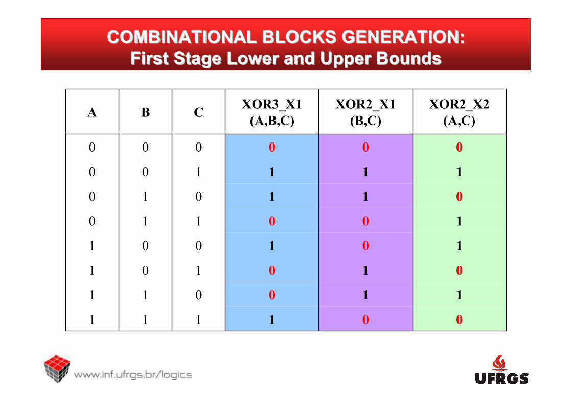
COMBINATIONAL BLOCKS GENERATION:COMBINATIONAL BLOCKS GENERATION:
First Stage Lower and Upper BoundsFirst Stage Lower and Upper Bounds

001111
110011
010101
101001
100110
011010
111100
000000
XOR2_X2
(A,C)
XOR2_X1
(B,C)
XOR3_X1
(A,B,C)CBA
COMBINATIONAL BLOCKS GENERATION:COMBINATIONAL BLOCKS GENERATION:
First Stage Lower and Upper BoundsFirst Stage Lower and Upper Bounds
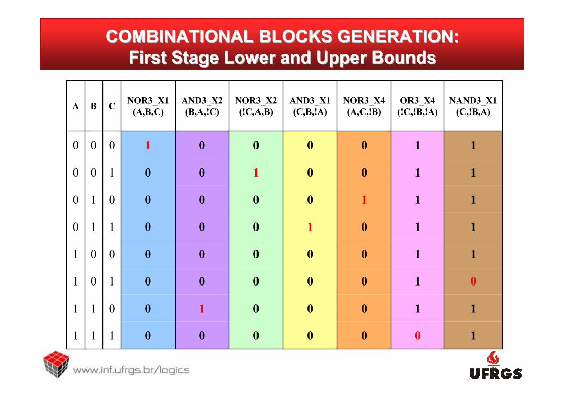
1000000111
1100010011
0100000101
1100000001
1101000110
1110000010
1100100100
1100001000
NAND3_X1
(C,!B,A)
OR3_X4
(!C,!B,!A)
NOR3_X4
(A,C,!B)
AND3_X1
(C,B,!A)
NOR3_X2
(!C,A,B)
AND3_X2
(B,A,!C)
NOR3_X1
(A,B,C)CBA
COMBINATIONAL BLOCKS GENERATION:COMBINATIONAL BLOCKS GENERATION:
First Stage Lower and Upper BoundsFirst Stage Lower and Upper Bounds
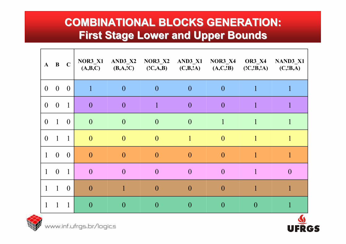
1000000111
1100010011
0100000101
1100000001
1101000110
1110000010
1100100100
1100001000
NAND3_X1
(C,!B,A)
OR3_X4
(!C,!B,!A)
NOR3_X4
(A,C,!B)
AND3_X1
(C,B,!A)
NOR3_X2
(!C,A,B)
AND3_X2
(B,A,!C)
NOR3_X1
(A,B,C)CBA
COMBINATIONAL BLOCKS GENERATION:COMBINATIONAL BLOCKS GENERATION:
First Stage Lower and Upper BoundsFirst Stage Lower and Upper Bounds
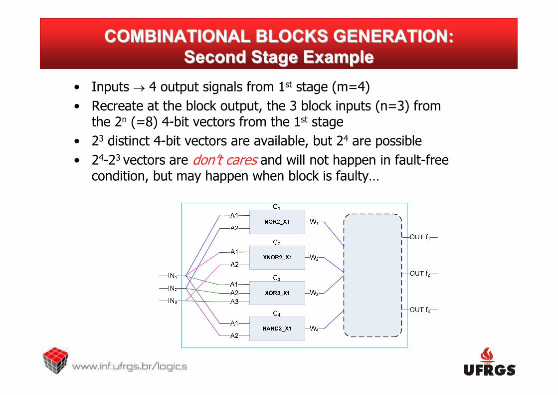
• Inputs → 4 output signals from 1st stage (m=4)
• Recreate at the block output, the 3 block inputs (n=3) from the 2n (=8) 4-bit vectors from the 1st stage
• 23 distinct 4-bit vectors are available, but 24 are possible
• 24-23 vectors are don’t cares and will not happen in fault-free condition, but may happen when block is faulty…
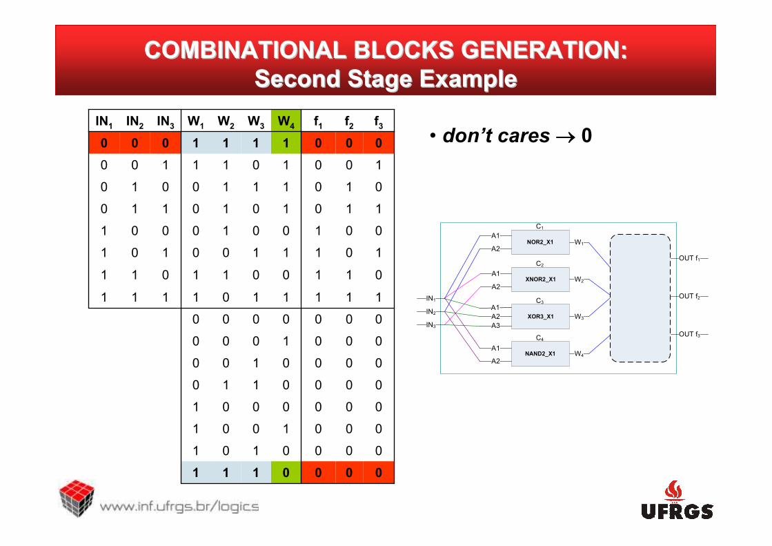
COMBINATIONAL BLOCKS GENERATION:COMBINATIONAL BLOCKS GENERATION:
Second Stage ExampleSecond Stage Example

XXX0111
XXX0101
XXX1001
XXX0001
XXX0110
XXX0100
XXX1000
XXX0000
1111101111
0110011011
1011100101
0010010001
1101010110
0101110010
1001011100
0001111000
f3f2f1W4W3W2W1IN3IN2IN1
COMBINATIONAL BLOCKS GENERATION:COMBINATIONAL BLOCKS GENERATION:
Second Stage ExampleSecond Stage Example
NAND2_X1
NOR2_X1
A2
A1
IN1
IN2
IN3
W1
W2
W3
W4
OUT f1
OUT f2
OUT f3
A1
A2
A1
C1
C2
C3
C4
XOR3_X1
XNOR2_X1
A2
A1
A3
A2
0000111
0000101
0001001
0000001
0000110
0000100
0001000
0000000
1111101111
0110011011
1011100101
0010010001
1101010110
0101110010
1001011100
0001111000
f3f2f1W4W3W2W1IN3IN2IN1
COMBINATIONAL BLOCKS GENERATION:COMBINATIONAL BLOCKS GENERATION:
Second Stage ExampleSecond Stage Example
NAND2_X1
NOR2_X1
A2
A1
IN1
IN2
IN3
W1
W2
W3
W4
OUT f1
OUT f2
OUT f3
A1
A2
A1
C1
C2
C3
C4
XOR3_X1
XNOR2_X1
A2
A1
A3
A2
• don’t cares→→→→ 0

0010111
0000101
0001001
0000001
0000110
0000100
0001000
0000000
1111101111
0110011011
1011100101
0010010001
1101010110
0101110010
1001011100
0001111000
f3f2f1W4W3W2W1IN3IN2IN1
COMBINATIONAL BLOCKS GENERATION:COMBINATIONAL BLOCKS GENERATION:
Second Stage ExampleSecond Stage Example
NAND2_X1
NOR2_X1
A2
A1
IN1
IN2
IN3
W1
W2
W3
W4
OUT f1
OUT f2
OUT f3
A1
A2
A1
C1
C2
C3
C4
XOR3_X1
XNOR2_X1
A2
A1
A3
A2
• don’t cares→→→→ 0
• single fault detection

34
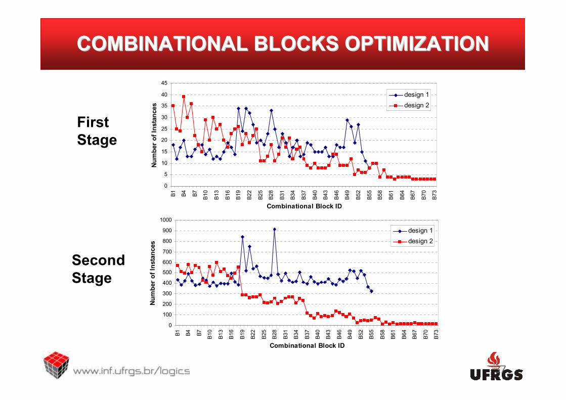
COMBINATIONAL BLOCKS OPTIMIZATIONCOMBINATIONAL BLOCKS OPTIMIZATION
•• Number of inputs/outputsNumber of inputs/outputs: reducing ‘n’ tends to reduce the
number of instantiated cells at the first stage ‘m’, and so the
W(m..1) vector size, which corresponds to the input data of
the second stage. It has impact in the second stage size.

35
COMBINATIONAL BLOCKS OPTIMIZATIONCOMBINATIONAL BLOCKS OPTIMIZATION
•• Number of inputs/outputsNumber of inputs/outputs: reducing ‘n’ tends to reduce the
number of instantiated cells at the first stage ‘m’, and so the
W(m..1) vector size, which corresponds to the input data of
the second stage. It has impact in the second stage size.
•• Cell orderingCell ordering: the cell list can be ordered by the number of
inputs in a decrescent way. Making so, the biggest cells are
used in the first blocks, and the inputs of blocks can decrease
at each new generation. The CB chain is still allowed.

36
COMBINATIONAL BLOCKS OPTIMIZATIONCOMBINATIONAL BLOCKS OPTIMIZATION
Design 1:
Design 2:
37
COMBINATIONAL BLOCKS OPTIMIZATIONCOMBINATIONAL BLOCKS OPTIMIZATION
0
100
200
300
400
500
600
700
800
900
1000
B1
B4
B7
B10
B13
B16
B19
B22
B25
B28
B31
B34
B37
B40
B43
B46
B49
B52
B55
B58
B61
B64
B67
B70
B73
Combinational Block ID
Number of Instances
design 1
design 2
0
5
10
15
20
25
30
35
40
45
B1
B4
B7
B10
B13
B16
B19
B22
B25
B28
B31
B34
B37
B40
B43
B46
B49
B52
B55
B58
B61
B64
B67
B70
B73
Combinational Block ID
Number of Instances
design 1
design 2
First
Stage
Second
Stage
38
COMBINATIONAL BLOCKS OPTIMIZATIONCOMBINATIONAL BLOCKS OPTIMIZATION
OUTLINEOUTLINE
• Introduction and motivation
• Goals of this work (design specification)
• Design of combinational blocks (key point)
• Circuit architecture and operation modes
• Conclusions and future works
39
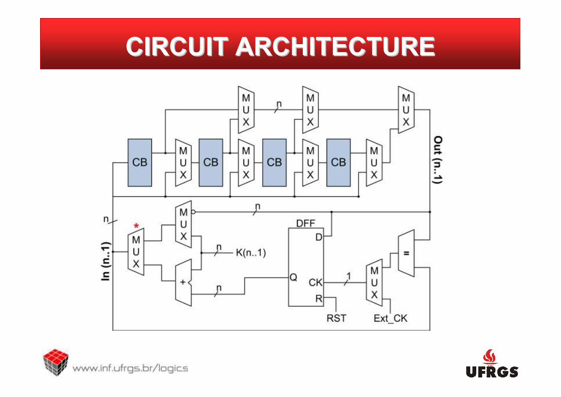
CIRCUIT ARCHITECTURECIRCUIT ARCHITECTURE
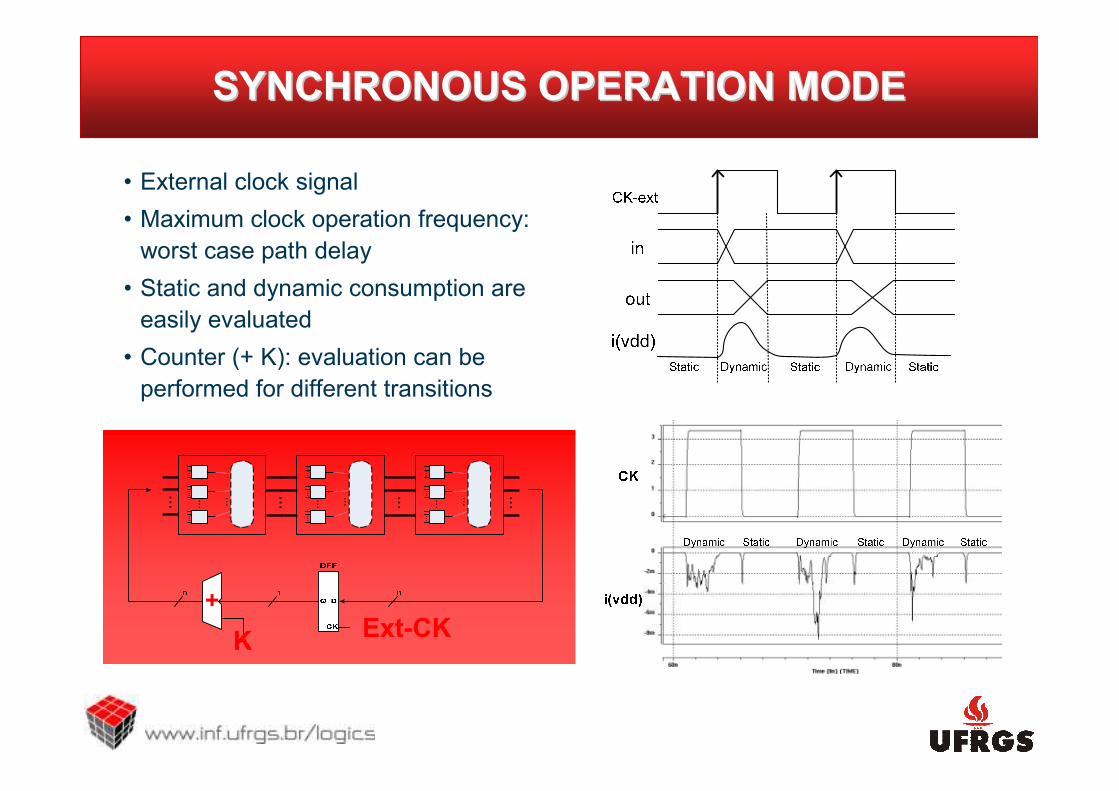
SYNCHRONOUS OPERATION MODESYNCHRONOUS OPERATION MODE
• External clock signal
• Maximum clock operation frequency:
worst case path delay
• Static and dynamic consumption are
easily evaluated
• Counter (+ K): evaluation can be
performed for different transitions
Ext-CKK
+

SELFSELF--TIMED OPERATION MODETIMED OPERATION MODE
n n n
DFF
Q D
K
CKn
n
1
Out(n..1)In(n..1)
M
U
X
Ext-CK
+
In(n..1)
Out(n..1)=
• Self-timed counter, no external stimuli
• X=Y → Ck=1 / X≠Y → Ck=0
• Functional cell verification
(self-checking: logic error → circuit stops)
• Aging effects: continuous operation (self-
timed performance degradation).
x y
x
y
synchronous mode self-timed mode
faultdetectio
n

OBIST OPERATION MODEOBIST OPERATION MODE
• No external stimulus needed
• Delay verification → like ring oscillator
• Delay propagation through a large number of different logic paths
• Logic and timing errors verification
• Particular MUX allows open chain test
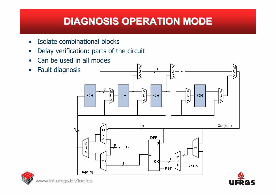
• Isolate combinational blocks
• Delay verification: parts of the circuit
• Can be used in all modes
• Fault diagnosis
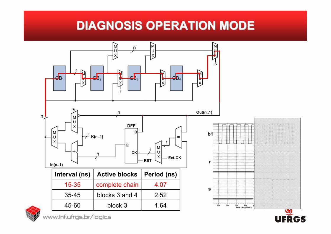
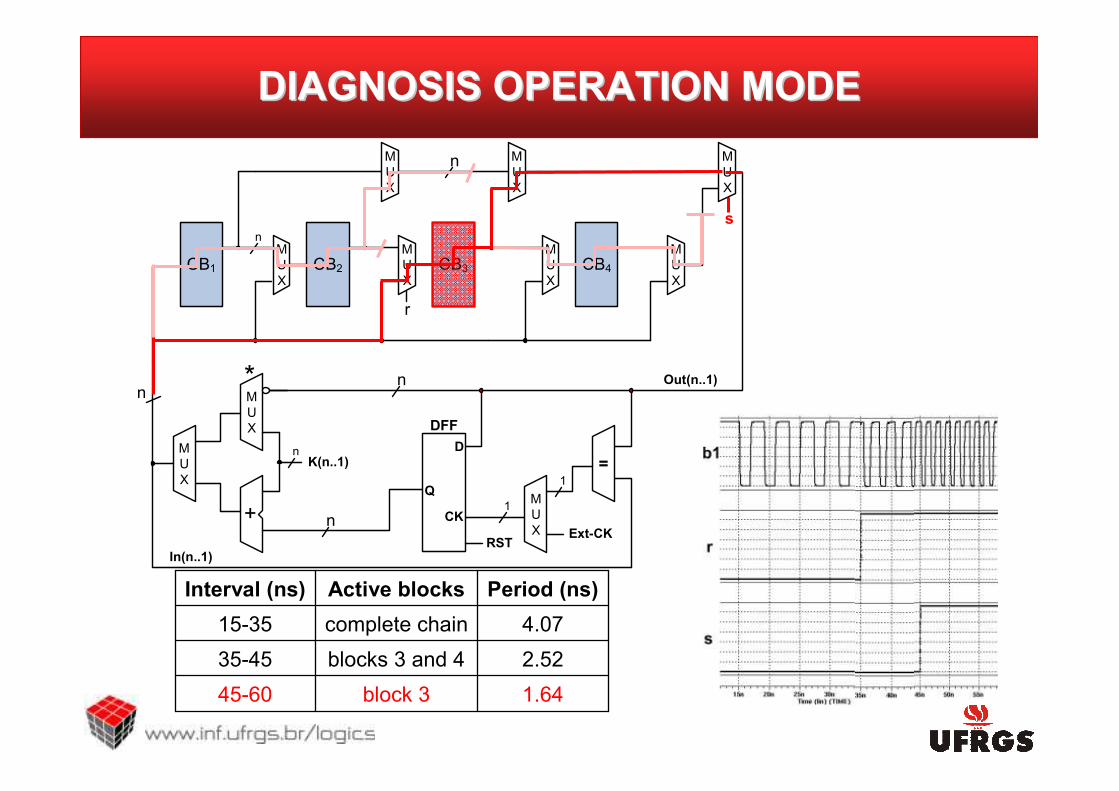
DIAGNOSIS OPERATION MODEDIAGNOSIS OPERATION MODE

1.64block 345-60
2.52blocks 3 and 435-45
4.07complete chain15-35
Period (ns)Active blocksInterval (ns)
DFF
M
U
X=
M
U
XCK
D
+
M
U
X
Q
Ext-CK
n
n
n
K(n..1)
1
1
n
RST
CB4CB3M
U
XCB2
M
U
XCB1
M
U
X
M
U
X
M
U
X
M
U
X
M
U
X
n
n
Out(n..1)
In(n..1)
*
r
s
DIAGNOSIS OPERATION MODEDIAGNOSIS OPERATION MODE
1.64block 345-60
2.52blocks 3 and 435-45
4.07complete chain15-35
Period (ns)Active blocksInterval (ns)
DFF
M
U
X=
M
U
XCK
D
+
M
U
X
Q
Ext-CK
n
n
n
K(n..1)
1
1
n
RST
CB4CB3M
U
XCB2
M
U
XCB1
M
U
X
M
U
X
M
U
X
M
U
X
M
U
X
n
n
Out(n..1)
In(n..1)
*
r
s
DIAGNOSIS OPERATION MODEDIAGNOSIS OPERATION MODE

1.64block 345-60
2.52blocks 3 and 435-45
4.07complete chain15-35
Period (ns)Active blocksInterval (ns)
DFF
M
U
X=
M
U
XCK
D
+
M
U
X
Q
Ext-CK
n
n
n
K(n..1)
1
1
n
RST
CB4CB3M
U
XCB2
M
U
XCB1
M
U
X
M
U
X
M
U
X
M
U
X
M
U
X
n
n
Out(n..1)
In(n..1)
*
r
s
r
DIAGNOSIS OPERATION MODEDIAGNOSIS OPERATION MODE
1.64block 345-60
2.52blocks 3 and 435-45
4.07complete chain15-35
Period (ns)Active blocksInterval (ns)
DFF
M
U
X=
M
U
XCK
D
+
M
U
X
Q
Ext-CK
n
n
n
K(n..1)
1
1
n
RST
CB4CB3M
U
XCB2
M
U
XCB1
M
U
X
M
U
X
M
U
X
M
U
X
M
U
X
n
n
Out(n..1)
In(n..1)
*
r
ss
DIAGNOSIS OPERATION MODEDIAGNOSIS OPERATION MODE
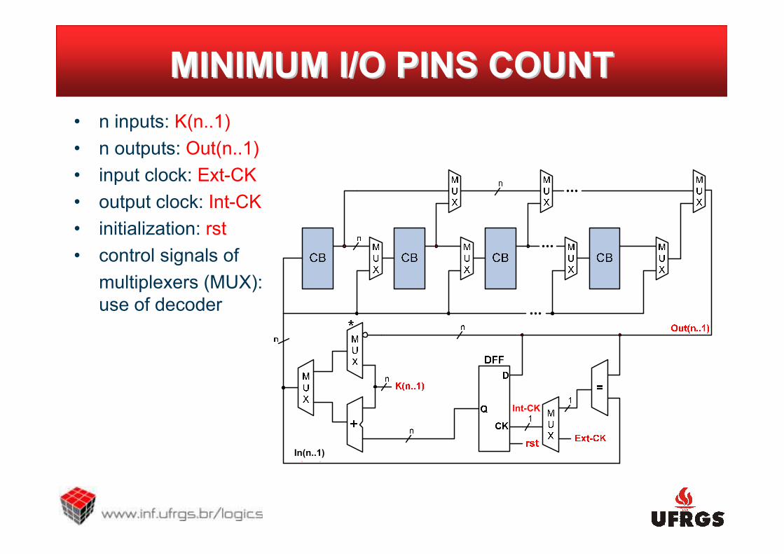
• n inputs: K(n..1)
• n outputs: Out(n..1)
• input clock: Ext-CK
• output clock: Int-CK
• initialization: rst
• control signals of
multiplexers (MUX):
use of decoder
In(n..1)
Int-CK
MINIMUM I/O PINS COUNTMINIMUM I/O PINS COUNT
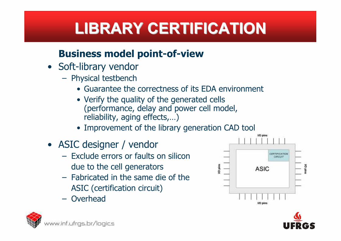
Business model point-of-view
• Soft-library vendor– Physical testbench
• Guarantee the correctness of its EDA environment
• Verify the quality of the generated cells (performance, delay and power cell model, reliability, aging effects,…)
• Improvement of the library generation CAD tool
• ASIC designer / vendor– Exclude errors or faults on silicon
due to the cell generators
– Fabricated in the same die of the
ASIC (certification circuit)
– Overhead
LIBRARY CERTIFICATIONLIBRARY CERTIFICATION
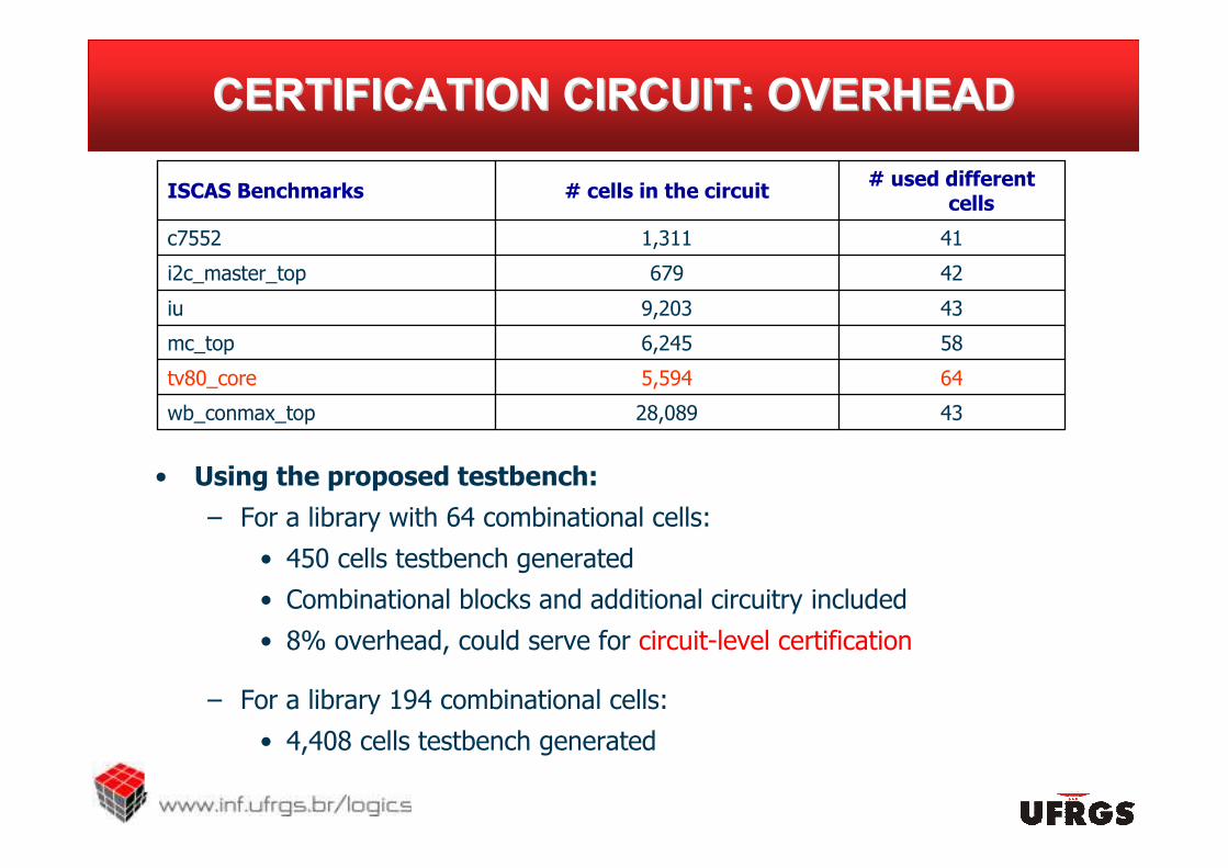
• Using the proposed testbench:
– For a library with 64 combinational cells:
• 450 cells testbench generated
• Combinational blocks and additional circuitry included
• 8% overhead, could serve for circuit-level certification
– For a library 194 combinational cells:
• 4,408 cells testbench generated
4328,089wb_conmax_top
645,594tv80_core
586,245mc_top
439,203iu
42679i2c_master_top
411,311c7552
# used differentcells
# cells in the circuitISCAS Benchmarks
CERTIFICATION CIRCUIT: OVERHEADCERTIFICATION CIRCUIT: OVERHEAD
• A test circuit (testbench) for IC design flow and on-
silicon for full verification and validation of an entire
set of combinational cells.
– CAD tool was developed in Java in order to automate the generation of combinational blocks.
– Different operating modes allow a large variety of timing and power measurements.
CONCLUSIONSCONCLUSIONS

For more information,contact:
AndrAndréé I. ReisI. Reis: [email protected]
RenatoRenato P. P. RibasRibas: [email protected]
www.inf.ufrgs.br/logics