Embed Size (px)
Citation preview

Content-aware Encoding for Improving Energy Efficiency in Multi-LevelCell Resistive Random Access Memory
Hadi Hajimiri, Prabhat MishraCISE, University of Florida{hadi, prabhat}@cise.ufl.edu
Swarup BhuniaEECS, Case Western Reserve University
Branden Long, Yibo Li, Rashmi JhaEECS, University of Toledo
Abstract— Memory is an integral and important component ofboth general-purpose and embedded systems. It is widely acknowl-edged that energy of the memory structure is a major contributor inoverall system energy. Recent advances with emerging non-volatilememory (NVM) technologies can potentially alleviate the issue ofmemory leakage power. However, they introduce new challengesand opportunities for dynamic power management in memory. Inthis paper, we consider resistive random access memory (RRAM),a promising NVM technology, and observe that a specific featureof the memory, namely, its multi-level cell (MLC) structure, canbe used to significantly reduce its read access energy. Unlike con-ventional CMOS static random access memory (SRAM), the readaccess energy in RRAM largely depend on the stored content. Basedon this observation, we present an efficient encoding technique forimproving the energy efficiency for multi-level cell RRAM. Oursimulation results with benchmark applications demonstrate anorder-of-magnitude energy reduction with modest area overhead.
I. INTRODUCTION
Power consumption has emerged as a primary designconstraint for both general-purpose and embedded systems.The active power in an integrated circuit (IC) comprises ofswitching (dynamic) power and active leakage in logic andmemory circuits. Reduction of active power has emergedas the primary design goal for the IC manufacturers andsystem designers to address the battery life issue in portablesystems and to mitigate the temperature induced reliabilityconcerns. Memory plays an important role in system energy,due to integration of increasingly larger memory closer to theprocessor in the memory hierarchy and faster memory clock.Hence, there is a critical need to significantly reduce activeenergy in memory. Memory active power has two components:1) active leakage (which is typically much higher than standbypower due to higher junction temperature in active mode); and2) the read/write access energy. In order to reduce memoryenergy significantly, one needs to address both the leakageand dynamic energy during read/write operations.
With CMOS technology rapidly approaching the end ofits roadmap [1], future computing systems are likely tobe built with emerging non-volatile memory (NVM) tech-nologies, such as resistive random access memory (RRAM)[7][8], spin torque transfer RAM (STTRAM) [11]-[13], phasechange memory (PCM) [10], which show promising density,read/write performance and endurance. Among these tech-nologies, RRAM has appeared highly promising primarilydue to the benefits in terms of its non-volatility, integrationdensity, read/write endurance, manufacturability, and accessperformance/energy. In recent times, various research efforts
This work was partially supported by NSF grants CNS-0746261, CCF-1218629, BRIGE 1125743, CCF-0964514 and ECCS-1002237.
have focused on RRAM fabrication, device modeling andoptimization, and circuit and system level performance/energyanalysis. However, circuit/architecture level design approachesfor minimizing memory energy for these devices have not beenadequately explored. In this paper, we study a specific charac-teristic of RRAM, namely its multi level cell (MLC) structurethat enables a cell to store more than one bit informationand is beneficial in greatly improving memory density. Next,we propose an architecture-level energy optimization approachthat exploits the MLC nature of the RRAM cells to drasticallyreduce the read access energy. This is in addition to the factthat the non-volatile nature of RRAM cells virtually eliminatesthe memory core leakage. This makes RRAM as an attractivechoice for implementing the memory arrays in a processormemory hierarchy.
Based on read/write process of RRAM memory cells, weexploit the intrinsically asymmetric nature of most NVM cellsin order to improve the energy efficiency while maintainingor improving access performance and integration density. Inparticular, we observe that MLC structures, which lead to largeimprovement in density, provide largely varying access energy.From the RRAM read operation we find that a smaller currentflows in the circuit corresponding to read “00” than read “11”.This is because the resistance of state “00” is higher than state“11”. A more resistive state with an identical voltage pulse willresult in a lower instantaneous power (V2/R) and therefore alower read energy. Our analysis with respect to read accessenergy in a resistive crossbar shows that reading “00” and “01”from MLC comes at several orders of magnitude less energythan reading “10” and “11” as shown in Fig. 1. In order toexploit the nature of MLC for improving energy-efficiency,we propose an efficient encoding technique based on bit flips.Our experimental results demonstrate an order-of-magnitudereduction in memory access energy.
The rest of the paper is organized as follows. SectionII presents an overview and contributions of our proposedapproach. We have surveyed the related work in Section III.In Section IV, we model energy consumption of RRAM cells.Section V describes our encoding-based energy optimizationtechnique. Section VI presents the experimental results fora set of benchmark applications. Section VII concludes thepaper.
II. OVERVIEW AND CONTRIBUTIONS
Fig. 2 shows the overall approach, which integrates memorycharacterization and power modeling with content-aware en-coding and subsequent system-level energy estimation steps.We study the effectiveness of the proposed encoding for MLC

10-20
10-18
10-16
10-14
10-12
-5 0 5 10 15 20
'00''01''10''11'
Ener
gy (J
)
Time (ns)
-0.10
0.10.20.30.40.50.6
10-7
10-6
10-5
0.0001
0.001
0.01
-5 0 5 10 15 20
Voltage (V) '00'
'01'
'10'
'11'
Volta
ge (V
) Current (A
)
Time (ns)
Fig. 1: Memory read access energy for RRAM MLC (2 bits percell) for four different states with a read-voltage pulse durationof 15ns. Read energy is calculated by first obtaining theresistance of the device in different states from experimentaldata (shown in Fig. 5 (a)) after programming the device indifferent states. These resistance values were then used alongwith the read-voltage pulse of amplitude 0.5 V, and width 15nsto get the instantaneous read currents, shown in the inset. Theinstantaneous read power was calculated and integrated alongthe pulse-width and plotted as read-energy vs. time over theentire 15ns pulse-width.
RRAM based main memory, although such an approach canbe used in other levels of memory hierarchy. As a by-product,RRAM array also helps to mitigate the memory leakageissue. Unlike alternative volatile memory technologies suchas SRAM and DRAM, which require constant connection toVDD to retain stored content, RRAM reduces the core leakagepower to virtually zero. This is consistent with other resistiveNVM technologies [17]. The leakage power of the read/writecircuitry remains comparable to that of a volatile memory.However, the leakage for a conventional SRAM-based memoryarray is typically dominated by the core. Hence, elimination ofcore leakage results in large saving in memory leakage. SinceRRAM does not incur any leakage overhead, reduction ofread energy consumption directly translates to overall energyefficiency for application binaries.
In a processor-based system, a large part of the memorydynamic energy is typically dissipated in reading data. Inparticular, for instructions of a program, there is no writingonce the program page is fetched to main memory from thelast level of memory. In our simulations with a set of mediabenchmarks, we observed 88.7% read operation comparedto 11.3% write operations in L2 cache. Hence, a system-level design approach that aims at minimizing the read accessenergy of embedded memory can translate to large savingin total energy. Based on the skewed content-dependent readenergy of RRAM devices, we infer that if the system is biasedfor reading more “00” than “11”s, we can have considerablesaving in total dynamic energy with RRAMs.
This analysis provides the motivation to encode information(both instruction and data) before storing them to memory in away that maximizes the “00” and “01” content in order to dra-matically improve the access energy. Interestingly, increasing
Characterize RRAM MLC Array
Develop Device Model &
Perform Power Analysis
Perform Content-Aware
Information Encoding
Perform System-Level Power
Simulations
Program
Benchmarks
Input
Dataset
MLC
Power
Model
Memory Access Energy,
Area Overhead
Processor
Config.
RRAM Array
Fig. 2: Overall flow for the proposed approach that leverageson intrinsic asymmetry of resistive memory.
“00” and “01” counts is also expected to have large positiveimpact in memory reliability. This is because storing a reducedrange of values improves the reliability of a multi-level cell,since variation-induced degradation in dynamic range (due toreduced ION /IOFF ) is not likely to cause failures in the cellsstoring “00” and “01”. We believe it would affect the read,write and data retention reliability of the memory cells. Inorder to exploit the nature of MLC in reliability and energy-efficiency simultaneously, we propose an efficient encodingtechnique based on bit flips at varying level of granularity. Itcan drastically reduce read access energy in RRAM array.
In particular, the paper makes following key contributions:1) It presents a study of read access energy of resistive
memory which shows a content-dependent variation inaccess energy due to corresponding variations in resistivestates. It models the access energy behavior for MLCRRAM cells for representative cell design.
2) Exploiting the skewed access energy pattern, it presentsa low-cost content-dependent information encoding ap-proach that aims at maximizing the memory accessenergy saving. To the best of our knowledge, this isthe first effort that aims at improving memory energyefficiency exploiting intrinsic asymmetry of MLC cells,which provide different read access energy depending onthe stored content.
III. RELATED WORK
Encoding techniques are widely used to achieve energy,area, reliability, and performance optimizations. Xie et al. [2]introduced a compression technique capable of compressingflexible instruction formats in VLIW architectures. Seong etal. [3] presented bitmask-based compression that improvesdictionary-based compression using bitmasks. Mirhoseini etal. [4] developed a novel coding method to minimize PhaseChange Memory (PCM) write energy. It minimizes the energyrequired for memory rewrites by utilizing the differencesbetween PCM read, set, and reset energies. S. Cho and Lee
[9] proposed Flip-N-Write to replace a PRAM write operationwith a more efficient read-modify-write operation. These tech-niques only consider write energy for single level cell PRAMmemory. In this work we present a content-aware encodingtechnique that optimizes the read energy (program and read-only data) utilizing the differences in energy of reading dif-ferent values in multilevel RRAM cells (MLC). The existingwrite-energy minimization techniques are complementary toour approach, and can be used together to reduce both readand write energy of memory in case of diverse datasets.
IV. RRAM POWER ANALYSIS
After an initial electroforming step by DC voltage sweep,the device was reset to high-resistance state (HRS) the statedenoted by 00. Fig. 3 (a) shows that low-resistance state (LRS)denoted by 11 can be achieved by setting the device using acompliance current of 5 mA and a different LRS denoted by10 can be achieved by setting the device using a compliancecurrent of 1 mA from an initial state of 00. Fig 3 (b) showsthat, HRS 00 and 01 could be achieved by resetting the devicefrom state 11 using reset voltages of -4.0 V and -2.6 V,respectively. The compliance currents were much higher thanthe desired values (< 100µA) due to larger dimensions ofthese devices.
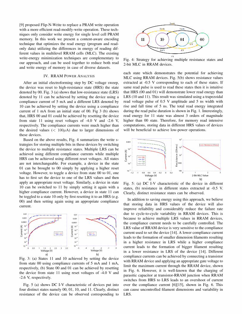
Based on the above results, Fig. 4 summarizes the write s-trategies for storing multiple bits in these devices by switchingthe device to multiple resistance states. Multiple LRS can beachieved using different compliance currents while multipleHRS can be achieved using different reset voltages. All statesare not interchangeable. For example, a device in the state01 can be brought to 00 simply by applying a higher resetvoltage. However, to toggle a device from state 00 to 01, onehas to first set the device to one of the LRS values and thenapply an appropriate reset voltage. Similarly, a device in state10 can be switched to 11 by simply setting it again with ahigher compliance current. However, a device in state 11 canbe toggled to a state 10 only by first resetting it to an HRS (e.g.00) and then setting again using an appropriate compliancecurrent.
10-10
10 -9
10 -8
10 -7
10 -6
10 -5
0.0001
0.001
0.01
0 0.5 1 1.5 2 2.5 3 3.5
1 mA5 mA
Curr
ent (
A)
Voltage (V)
10-10
10 -9
10 -8
10 -7
10 -6
10 -5
0.0001
0.001
0.01
-5 -4 -3 -2 -1 0
-4 V-2.6 V
Curr
ent (
A)
Voltage (V)
b)a)Fig. 3: (a) States 11 and 10 achieved by setting the devicefrom state 00 using compliance currents of 5 mA and 1 mA,respectively, (b) State 00 and 01 can be achieved by resettingthe device from state 11 using reset voltages of -4.0 V and-2.6 V, respectively.
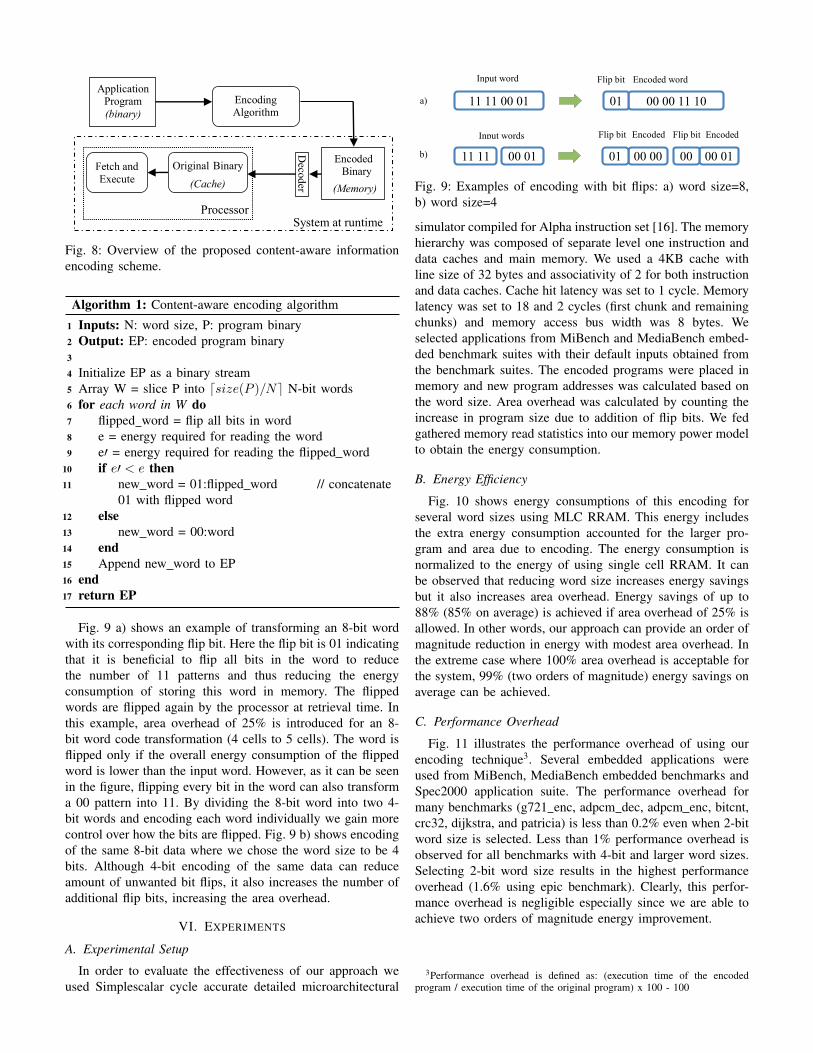
Fig. 5 (a) shows DC I-V characteristic of devices put intofour distinct states namely 00, 01, 10, and 11. Clearly, distinctresistance of the device can be observed corresponding to
Fig. 4: Strategy for achieving multiple resistance states and2-bit MLC in RRAM devices.
each state which demonstrates the potential for achievingMLC using RRAM devices. Fig. 5(b) shows resistance valuesextracted at -0.5 V corresponding to each of these states. Ifsame read pulse is used to read these states then it is intuitivethat HRS (00 and 01) will demonstrate lower read energy thanLRS (10 and 11). This result was simulated using a trapezoidalread voltage pulse of 0.5 V amplitude and 5 ns width withrise and fall time of 5 ns. The total read energy integratedduring the read pulse duration is shown in Fig. 1. Interestingly,read energy for 11 state was almost 3 orders of magnitudehigher than 00 state. Therefore, for memory read intensivecomputations, storing data in different HRS values of deviceswill be beneficial to achieve low-power operations.
10-11
10 -9
10 -7
10 -5
0.001
-1.2 -1 -0.8 -0.6 -0.4 -0.2 0 0.2
'00''01''10''11'
Curr
ent (
A)
Voltage (V)
100
1000
104
105
106
0 1 2 3
Resistance (Ohms))sm
hO( ec
natsiseR
2-Bit MLC Value
a) b)Fig. 5: (a) DC I-V characteristic of the device in differentstates, (b) resistance in different states extracted at -0.5 V.Clearly, distinct resistance states can be observed.
In addition to saving energy using this approach, we believethat storing data in HRS values of the device will alsoimprove reliability and considerably reduce the failure ratedue to cycle-to-cycle variability in RRAM devices. This isbecause to achieve multiple LRS values in RRAM devices,the compliance current needs to be carefully controlled. TheLRS value of RRAM device is very sensitive to the compliancecurrent used to set the device [14]. A lower compliance currentleads to the formation of smaller dimension filaments resultingin a higher resistance in LRS while a higher compliancecurrent leads to the formation of bigger filament resultingin a lower resistance in LRS of the device [14]. Differentcompliance currents can be achieved by connecting a transistorwith RRAM device and applying an appropriate gate voltage tolimit the maximum current through the RRAM device, shownin Fig. 6. However, it is well-known that the charging ofparasitic capacitor at transistor-RRAM junction when RRAMswitches from HRS to LRS leads to an overshoot of currentover the compliance current [6][15], shown in Fig. 6. Thiscan cause uncontrolled filament dimensions and variability inLRS.
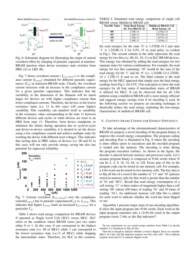
Fig. 6: Schematic diagram for illustrating the origin of currentovershoot effect by charging of parasitic capacitor at transitor-RRAM junction when device resistance state switches fromHRS (A) to LRS (B).
Fig. 7 shows overshoot current ( Iovershoot) vs. the compli-ance current (Icomp) simulated for different parasitic capaci-tances (Cp) at transistor-RRAM node. Clearly, the overshootcurrent increases with an increase in the compliance currentfor a given parasitic capacitance. This indicates that thevariability in the dimension of the filament will be muchlarger for devices set with higher compliance current thanlower compliance currents. Therefore, the devices in the lowestresistance states (i.e. 11 in this case) will cause highestvariability. This variability can manifest itself as variabilityin the resistance value corresponding to the state 11 betweendifferent devices and cycles or when devices are reset to anHRS from state 11. Therefore, from device standpoint, tominimize the failure during operation due to cycle-to-cycleand device-to-device variability, it is desired to set the deviceusing a low compliance current and achieve multiple states byresetting the device with different reset voltages. This indicatesthat storing data in HRS values of devices (i.e. 00 and 01 inthis case) will not only provide energy saving but also haspotential for improved reliability.
0
50
100
150
200
0 200 400 600 800 1000 1200
No Cp
Cp = 2.2 pF
Cp = 5 pF
Cp = 10 pF
Cp = 20 pF
Cp = 50 pF
Cp = 100 pF
I over
shoo
t (uA
)
Icomp
(uA)
SimulationV
set = 0.6 V
Fig. 7: Current overshoot (Iovershoot) over the compliancecurrent(Icomp) due to parasitic capacitance(Cp) vs. Icomp. Thisindicates that higher Icomp leads an increased Iovershoot for aparticular Cp.
Table I shows read energy comparison for RRAM devicesif operated as Single Level Cell (SLC) versus MLC. SLCrefers to the condition where RRAM stores just two stateseither 0 or 1. In this case, 0 can correspond to the highestresistance state (i.e. 00 of MLC) while 1 can correspond tothe lowest resistance state (i.e.11 of MLC) while skippingthe intermediate states. Therefore, for SLC in this scenario,
TABLE I: Simulated read energy comparison of single cellRRAM versus Multilevel RRAM cell.
Two-Bit Value Total Read Energy Multilevel RRAM Cellfor Two-RRAM (J) Read Energy (J)
‘00’ 2.54E-14 1.2702e-14‘01’ 1.25E-11 9.9770e-14‘10’ 1.25E-11 1.2577e-12‘11’ 2.49E-11 1.2438e-11
the read energies for the state ‘0’ is 1.2702E-14 J and state‘1’ is 1.2438E-11 J for 0.5V, 15 ns read pulse, as evidentin Fig.1. The second column in the table represents the readenergy for two-bits (i.e. 00, 01, 10, 11) in SLC RRAM devices.This energy was obtained by adding the read energies for twoseparate states for various combinations. For example, the readenergy for two bits containing ‘10’ would be the sum of theread energy for bit ‘1’ and bit ‘0’ (i.e. 1.2438E-11+1.2702E-14 = 1.25E-11 J) and so on. The third column is the readenergy for the MLC approach that simply uses the final energyreadings from Fig.1. for 0.5V, 15ns read-pulse to show the readenergies for all four states if intermediate states of RRAMis utilized for MLC. It can be observed that for all 2-bitpatterns using a multilevel RRAM cell is more energy efficientand suggests energy savings even if no encoding is used. Inthe following section we propose an encoding technique todrastically reduce the read energy exploiting the low-energycharacteristic of multilevel RRAM cell.
V. CONTENT-AWARE CODING FOR ENERGY EFFICIENCY
To take advantage of the aforementioned characteristics ofRRAM we propose a novel encoding of the program binary toimprove the overall energy consumption. The program codingand decoding flow is illustrated in Fig. 8 where the encodingis done offline (prior to execution) and the encoded programis loaded into the memory. The decoding is done duringthe program execution (online). As shown in the figure, thedecoder is placed between memory and processor cache. Let’sassume program binary is composed of N-bit words where Ncan be 2, 4, 8, 16, 32, 64, or 128. Every pair of bits in theprogram code can be stored in one memory cell. For example,a 4-bit word can be stored in two memory cells. The key idea isto flip all bits of a word if the number of ‘11’ and ‘10’ patternsstored in memory cells for that word is greater than the numberof ‘01 and ‘00’s1. Recall that read energy consumption of acell storing ‘11’ is three orders-of-magnitude higher than a cellstoring ‘00’ (about 100 times of reading ‘01’ and 10 times ofreading ‘10’). An additional memory cell (flip bit) is addedfor each word to indicate whether the word has been flippedor not.
Algorithm 1 presents major steps of our encoding algorithm.It slices the input program into N-bit words. Each word in theinput program translates into a (2+N)-bit word in the outputprogram (extra 2 bits as the flip indicator)2.
1In our experiments we use actual energy numbers from Table I to decidewhether it is beneficial to flip all bits.
2One bit is enough to indicate whether a word is flipped. Since we considerMLCs of 2 bits, the flip indicator requires two bits (one cell) – 00 to indicateoriginal word and 01 to indicate flipped word.
Application Program (binary)
Encoded Binary
(Memory)
Encoding Algorithm
Original Binary (Cache)
System at runtime
Fetch and Execute
Decoder
Processor
Fig. 8: Overview of the proposed content-aware informationencoding scheme.
Algorithm 1: Content-aware encoding algorithm
1 Inputs: N: word size, P: program binary2 Output: EP: encoded program binary3
4 Initialize EP as a binary stream5 Array W = slice P into dsize(P )/Ne N-bit words6 for each word in W do7 flipped word = flip all bits in word8 e = energy required for reading the word9 e′ = energy required for reading the flipped word
10 if e′ < e then11 new word = 01:flipped word // concatenate
01 with flipped word12 else13 new word = 00:word14 end15 Append new word to EP16 end17 return EP
Fig. 9 a) shows an example of transforming an 8-bit wordwith its corresponding flip bit. Here the flip bit is 01 indicatingthat it is beneficial to flip all bits in the word to reducethe number of 11 patterns and thus reducing the energyconsumption of storing this word in memory. The flippedwords are flipped again by the processor at retrieval time. Inthis example, area overhead of 25% is introduced for an 8-bit word code transformation (4 cells to 5 cells). The word isflipped only if the overall energy consumption of the flippedword is lower than the input word. However, as it can be seenin the figure, flipping every bit in the word can also transforma 00 pattern into 11. By dividing the 8-bit word into two 4-bit words and encoding each word individually we gain morecontrol over how the bits are flipped. Fig. 9 b) shows encodingof the same 8-bit data where we chose the word size to be 4bits. Although 4-bit encoding of the same data can reduceamount of unwanted bit flips, it also increases the number ofadditional flip bits, increasing the area overhead.
VI. EXPERIMENTS
A. Experimental Setup
In order to evaluate the effectiveness of our approach weused Simplescalar cycle accurate detailed microarchitectural
11 11 00 01 00 00 11 10 01 01
Input word Flip bit Encoded word
00 01 00 00 01 01
Input words Flip bit Encoded
a)
11 11 00 01 00 01
Flip bit Encoded b)
Fig. 9: Examples of encoding with bit flips: a) word size=8,b) word size=4
simulator compiled for Alpha instruction set [16]. The memoryhierarchy was composed of separate level one instruction anddata caches and main memory. We used a 4KB cache withline size of 32 bytes and associativity of 2 for both instructionand data caches. Cache hit latency was set to 1 cycle. Memorylatency was set to 18 and 2 cycles (first chunk and remainingchunks) and memory access bus width was 8 bytes. Weselected applications from MiBench and MediaBench embed-ded benchmark suites with their default inputs obtained fromthe benchmark suites. The encoded programs were placed inmemory and new program addresses was calculated based onthe word size. Area overhead was calculated by counting theincrease in program size due to addition of flip bits. We fedgathered memory read statistics into our memory power modelto obtain the energy consumption.
B. Energy Efficiency
Fig. 10 shows energy consumptions of this encoding forseveral word sizes using MLC RRAM. This energy includesthe extra energy consumption accounted for the larger pro-gram and area due to encoding. The energy consumption isnormalized to the energy of using single cell RRAM. It canbe observed that reducing word size increases energy savingsbut it also increases area overhead. Energy savings of up to88% (85% on average) is achieved if area overhead of 25% isallowed. In other words, our approach can provide an order ofmagnitude reduction in energy with modest area overhead. Inthe extreme case where 100% area overhead is acceptable forthe system, 99% (two orders of magnitude) energy savings onaverage can be achieved.
C. Performance Overhead
Fig. 11 illustrates the performance overhead of using ourencoding technique3. Several embedded applications wereused from MiBench, MediaBench embedded benchmarks andSpec2000 application suite. The performance overhead formany benchmarks (g721 enc, adpcm dec, adpcm enc, bitcnt,crc32, dijkstra, and patricia) is less than 0.2% even when 2-bitword size is selected. Less than 1% performance overhead isobserved for all benchmarks with 4-bit and larger word sizes.Selecting 2-bit word size results in the highest performanceoverhead (1.6% using epic benchmark). Clearly, this perfor-mance overhead is negligible especially since we are able toachieve two orders of magnitude energy improvement.
3Performance overhead is defined as: (execution time of the encodedprogram / execution time of the original program) x 100 - 100
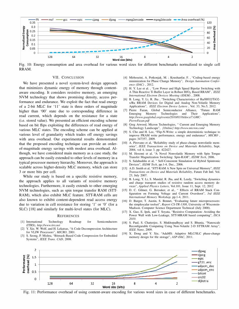
Fig. 10: Energy consumption and area overhead for various word sizes for different benchmarks normalized to single cellRRAM.
VII. CONCLUSION
We have presented a novel system-level design approachthat minimizes dynamic energy of memory through content-aware encoding. It considers resistive memory, an emergingNVM technology that shows promising density, access per-formance and endurance. We exploit the fact that read energyof a 2-bit MLC for ‘11’ state is three orders of magnitudehigher than ‘00’ state due to corresponding difference inread current, which depends on the resistance for a state(i.e. stored value). We presented an efficient encoding schemebased on bit flips exploiting the differences of read energy ofvarious MLC states. The encoding scheme can be applied atvarious level of granularity which trades off energy savingswith area overhead. Our experimental results demonstratedthat the proposed encoding technique can provide an order-of-magnitude energy savings with modest area overhead. Al-though, we have considered main memory as a case study, theapproach can be easily extended to other levels of memory in atypical processor memory hierarchy. Moreover, the approach isscalable across higher-density MLC memory, which can store3 or more bits per cell.
While our study is based on a specific resistive memory,the approach applies to all variants of resistive memorytechnologies. Furthermore, it easily extends to other emergingNVM technologies, such as spin torque transfer RAM (STT-RAM), which also exhibit MLC feature. STT-RAM cells arealso known to exhibit content-dependent read access energydue to variation in cell resistance for storing ‘1’ or ‘0’ (for aSLC) [18] and similarly for multi-level states (for MLC).
REFERENCES
[1] International Technology Roadmap for Semiconductors(ITRS), http://www.itrs.net
[2] Y. Xie, W. Wolf, and H. Lekatsas, “A Code Decompression Architecturefor VLIW Processors”, MICRO, 2001.
[3] S. Seong, P. Mishra, “Bitmask-Based Code Compression for EmbeddedSystems”, IEEE Trans. CAD, 2008.
[4] Mirhoseini, A. Potkonjak, M. ; Koushanfar, F. , “Coding-based energyminimization for Phase Change Memory”, Design Automation Confer-ence (DAC) , 2012.
[5] H. Y. Lee et al. , “Low Power and High Speed Bipolar Switching withA Thin Reactive Ti Buffer Layer in Robust HfO2 Based RRAM”, IEEEInternational Electron Devices Meeting (IDEM) , 2008.
[6] B. Long, Y. Li, R. Jha , “Switching Characteristics of Ru/HfO2/TiO2-x/Ru RRAM Devices for Digital and Analog Non-Volatile MemoryApplications”, IEEE Electron Device Letters , Vol. 33, No.5, 2012.
[7] Pierre Fazan, Global Semiconductor Alliance, “Future RAMEmerging Memory Technologies and Their Applications”,http://www.gsaglobal.org/events/2010/0316/docs/7.GMC-PierreFazan.pdf
[8] Greg Atwood, Micron Technologies, “ Current and Emerging MemoryTechnology Landscape”, [Online] http://www.micron.com/
[9] S. Cho and H. Lee, “Flip-N-Write: a simple deterministic technique toimprove PRAM write performance, energy and endurance”, MICRO ,pages 347357, 2009.
[10] A. Pirovano et al, “Reliability study of phase-change nonvolatile mem-ories”, IEEE Transactions on Device and Materials Reliability, Sept.2004, vol 4, issue 3, pp. 422427.
[11] M. Hosomi et al, “A Novel Nonvolatile Memory with Spin TorqueTransfer Magnetization Switching: Spin-RAM”, IEDM Tech, 2006.
[12] S. Salahuddin et al, “ Self-Consistent Simulation of Hybrid SpintronicDevices”, IEDM Tech, pp.1-4, Dec., 2006.
[13] A.D. Smith et al, “STT-RAM A New Spin on Universal Memory”, IEEETransactions on Device and Materials Reliability, Future Fab Intl. Vol.23, July 2007.
[14] B. Long, Y. Li, S. Mandal, R. Jha, and K. Leedy, “Switching dynamicsand charge transport studies of resistive random access memory de-vices”, Applied Physics Letters, Vol.101, Issue 11, Sept. 12, 2012
[15] D. C. Gilmer, G. Bersuker, et al., “ Effects of RRAM Stack Con-figuration on Forming Voltage and Current Overshoot”, 3rd IEEEInternational Memory Workshop, pp.1-4, 2011.
[16] D. Burger, T. Austin, S. Bennet, “Evaluating future microprocessors:the simplescalar toolset”, Report CS-TR-1308, University of Wisconsin-Madison. Computer Science Department Technical (July 2000).
[17] X. Guo, E. Ipek, and T. Soyata, “Resistive Computation: Avoiding thePower Wall with Low-Leakage, STT-MRAM based computing”, ISCA2010.
[18] S. Paul, S. Chatterjee, S. Mukhopadhyay and S. Bhunia, “NanoscaleReconfigurable Computing Using Non-Volatile 2-D STTRAM Array”,IEEE Nano, 2009.
[19] X. Dong and Y. Xie, “AdaMS: Adaptive MLC/SLC phase-changememory design for file storage”, ASP-DAC, 2011.
Fig. 11: Performance overhead of using content-aware encoding for various word sizes in case of different benchmarks.