Embed Size (px)
Citation preview
Construction Guide of High-Performance 4-Band Backpack
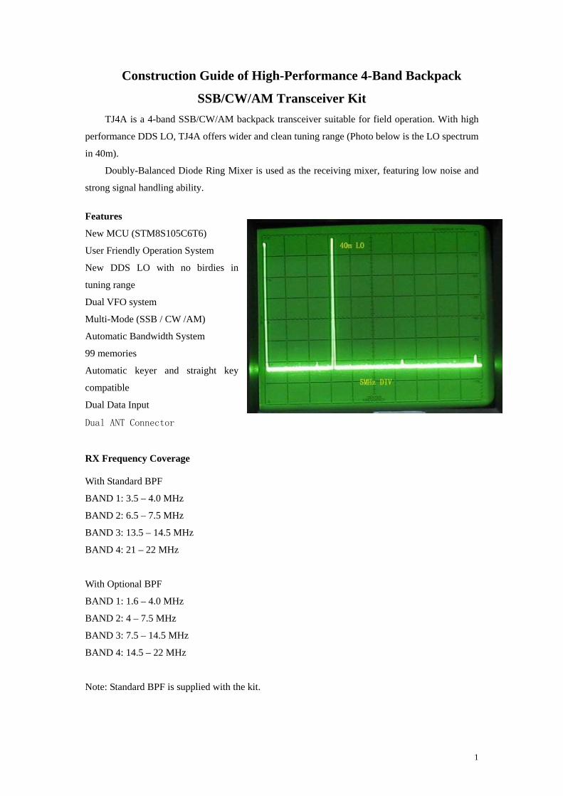
SSB/CW/AM Transceiver Kit TJ4A is a 4-band SSB/CW/AM backpack transceiver suitable for field operation. With high
performance DDS LO, TJ4A offers wider and clean tuning range (Photo below is the LO spectrum
in 40m).
Doubly-Balanced Diode Ring Mixer is used as the receiving mixer, featuring low noise and
strong signal handling ability.
Features
New MCU (STM8S105C6T6)
User Friendly Operation System
New DDS LO with no birdies in
tuning range
Dual VFO system
Multi-Mode (SSB / CW /AM)
Automatic Bandwidth System
99 memories
Automatic keyer and straight key
compatible
Dual Data Input
Dual ANT Connector
RX Frequency Coverage With Standard BPF
BAND 1: 3.5 – 4.0 MHz
BAND 2: 6.5 – 7.5 MHz
BAND 3: 13.5 – 14.5 MHz
BAND 4: 21 – 22 MHz
With Optional BPF
BAND 1: 1.6 – 4.0 MHz
BAND 2: 4 – 7.5 MHz
BAND 3: 7.5 – 14.5 MHz
BAND 4: 14.5 – 22 MHz
Note: Standard BPF is supplied with the kit.
1
TX Frequency Coverage With Standard BPF
BAND 1: 3.5 – 4.0 MHz
BAND 2: 7 – 7.5 MHz
BAND 3: 14 – 14.5 MHz
BAND 4: 21 – 21.5 MHz
Sensitivity
0.3 uV
Band Width
SSB: 2.1 KHz
CW: 1 KHz
AM: 6 KHz
Power Output
20 W
Note: Output power is adjustable.
Power Supply
10 V – 12.5 V
2
Construction
Coils
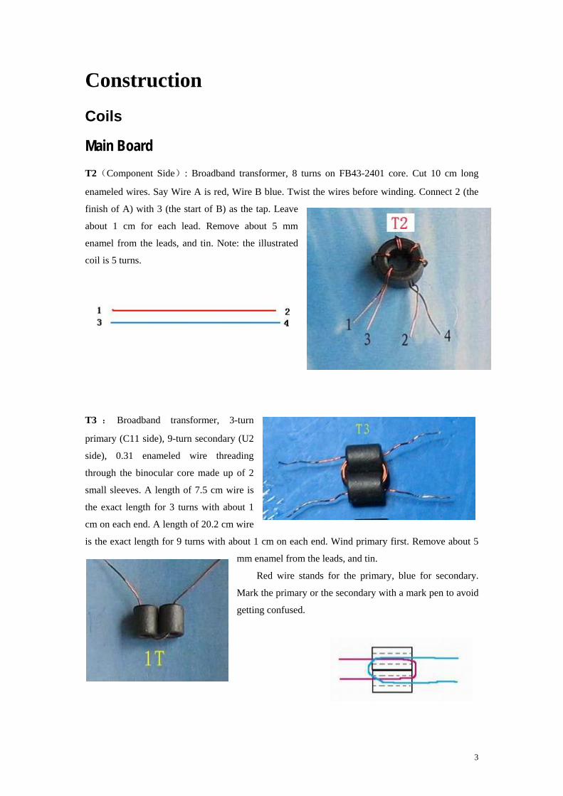
Main Board T2(Component Side): Broadband transformer, 8 turns on FB43-2401 core. Cut 10 cm long
enameled wires. Say Wire A is red, Wire B blue. Twist the wires before winding. Connect 2 (the
finish of A) with 3 (the start of B) as the tap. Leave
about 1 cm for each lead. Remove about 5 mm
enamel from the leads, and tin. Note: the illustrated
coil is 5 turns.
T3 : Broadband transformer, 3-turn
primary (C11 side), 9-turn secondary (U2
side), 0.31 enameled wire threading
through the binocular core made up of 2
small sleeves. A length of 7.5 cm wire is
the exact length for 3 turns with about 1
cm on each end. A length of 20.2 cm wire
is the exact length for 9 turns with about 1 cm on each end. Wind primary first. Remove about 5
mm enamel from the leads, and tin.
Red wire stands for the primary, blue for secondary.
Mark the primary or the secondary with a mark pen to avoid
getting confused.
3
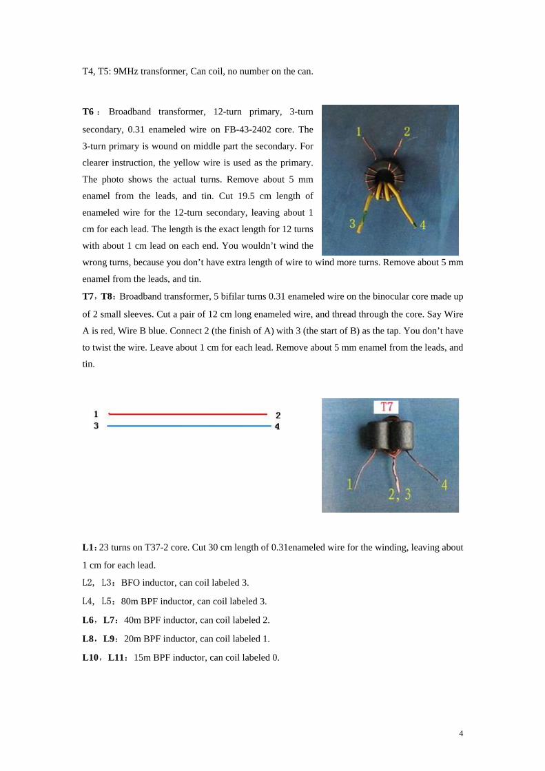
T4, T5: 9MHz transformer, Can coil, no number on the can.
T6 : Broadband transformer, 12-turn primary, 3-turn
secondary, 0.31 enameled wire on FB-43-2402 core. The
3-turn primary is wound on middle part the secondary. For
clearer instruction, the yellow wire is used as the primary.
The photo shows the actual turns. Remove about 5 mm
enamel from the leads, and tin. Cut 19.5 cm length of
enameled wire for the 12-turn secondary, leaving about 1
cm for each lead. The length is the exact length for 12 turns
with about 1 cm lead on each end. You wouldn’t wind the
wrong turns, because you don’t have extra length of wire to wind more turns. Remove about 5 mm
enamel from the leads, and tin.
T7,T8:Broadband transformer, 5 bifilar turns 0.31 enameled wire on the binocular core made up
of 2 small sleeves. Cut a pair of 12 cm long enameled wire, and thread through the core. Say Wire
A is red, Wire B blue. Connect 2 (the finish of A) with 3 (the start of B) as the tap. You don’t have
to twist the wire. Leave about 1 cm for each lead. Remove about 5 mm enamel from the leads, and
tin.
L1:23 turns on T37-2 core. Cut 30 cm length of 0.31enameled wire for the winding, leaving about
1 cm for each lead.
L2, L3:BFO inductor, can coil labeled 3.
L4, L5:80m BPF inductor, can coil labeled 3.
L6,L7:40m BPF inductor, can coil labeled 2.
L8,L9:20m BPF inductor, can coil labeled 1.
L10,L11:15m BPF inductor, can coil labeled 0.
4
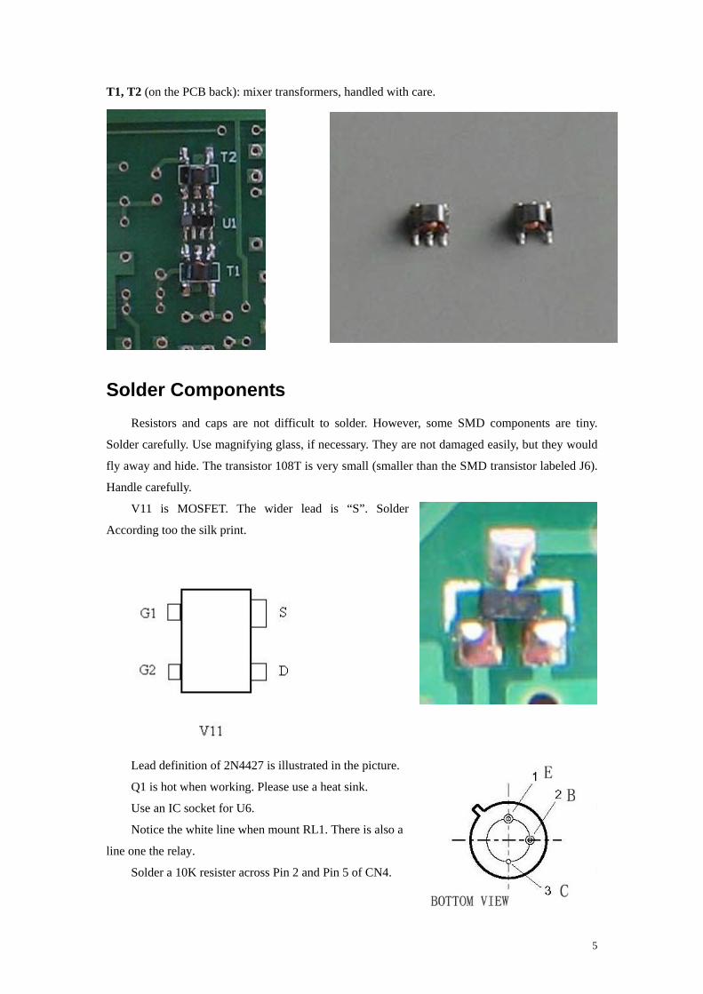
T1, T2 (on the PCB back): mixer transformers, handled with care.
Solder Components Resistors and caps are not difficult to solder. However, some SMD components are tiny.
Solder carefully. Use magnifying glass, if necessary. They are not damaged easily, but they would
fly away and hide. The transistor 108T is very small (smaller than the SMD transistor labeled J6).
Handle carefully.
V11 is MOSFET. The wider lead is “S”. Solder
According too the silk print.
Lead definition of 2N4427 is illustrated in the picture.
Q1 is hot when working. Please use a heat sink.
Use an IC socket for U6.
Notice the white line when mount RL1. There is also a
line one the relay.
Solder a 10K resister across Pin 2 and Pin 5 of CN4.
5
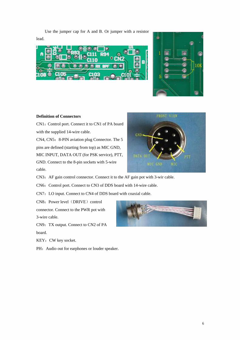
Use the jumper cap for A and B. Or jumper with a resistor
lead.
Definition of Connectors
CN1:Control port. Connect it to CN1 of PA board
with the supplied 14-wire cable.
CN4, CN5:8-PIN aviation plug Connector. The 5
pins are defined (starting from top) as MIC GND,
MIC INPUT, DATA OUT (for PSK service), PTT,
GND. Connect to the 8-pin sockets with 5-wire
cable.
CN3:AF gain control connector. Connect it to the AF gain pot with 3-wir cable.
CN6:Control port. Connect to CN3 of DDS board with 14-wire cable.
CN7:LO input. Connect to CN4 of DDS board with coaxial cable.
CN8:Power level(DRIVE)control
connector. Connect to the PWR pot with
3-wire cable.
CN9:TX output. Connect to CN2 of PA
board.
KEY:CW key socket.
PH:Audio out for earphones or louder speaker.
6
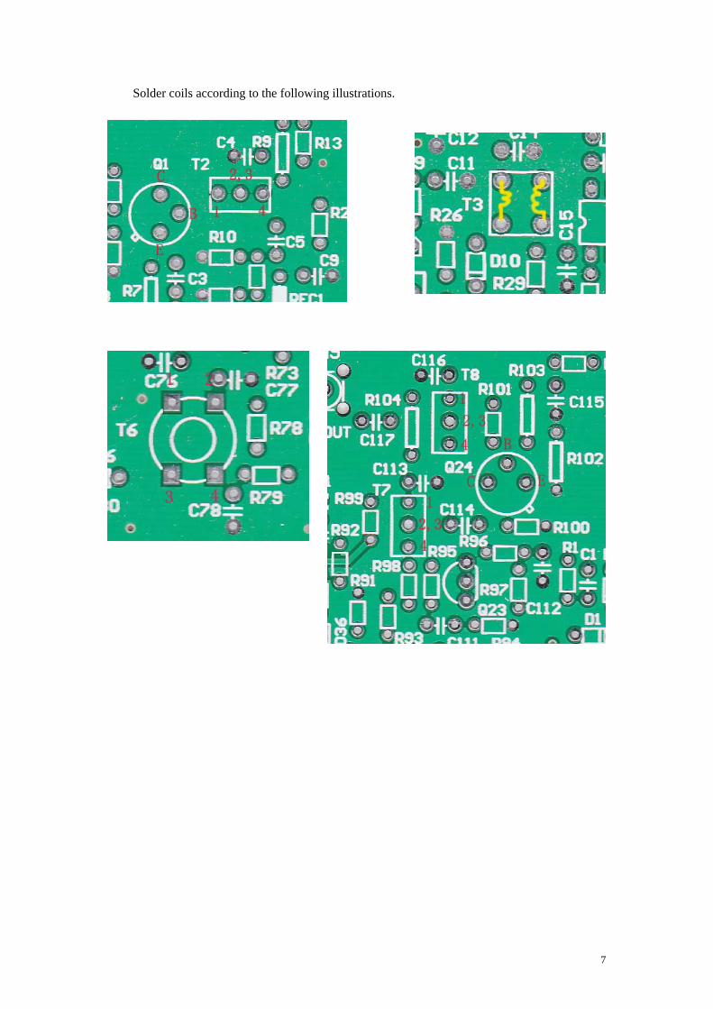
Solder coils according to the following illustrations.
7
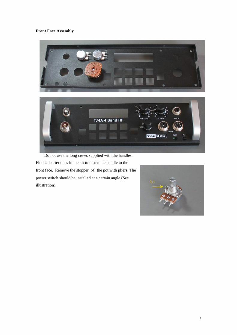
Front Face Assembly
nd
Do not use the long crews supplied with the handles.
Fi 4 shorter ones in the kit to fasten the handle to the
front face. Remove the stopper of the pot with pliers. The
power switch should be installed at a certain angle (See
illustration).
8
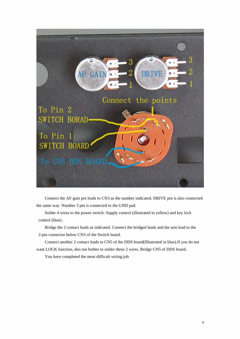
Connect the AF gain pot leads to CN3 as the number indicated. DRIVE pot is also connected
the same way. Number 3 pin is connected to the GND pad.
Solder 4 wires to the power switch: Supply control (illustrated in yellow) and key lock
control (blue) .
Bridge the 2 contact leads as indicated. Connect the bridged leads and the arm lead to the
2-pin connector below CN3 of the Switch board.
Connect another 2 contact leads to CN5 of the DDS board(Illustrated in blue).If you do not
want LOCK function, doo not bother to solder these 2 wires. Bridge CN5 of DDS board.
You have completed the most difficult wiring job.
9
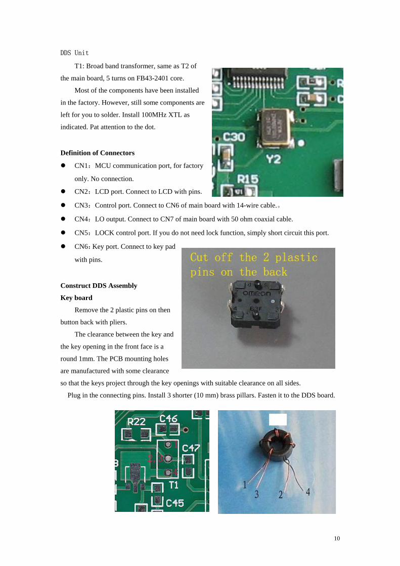
DDS Unit
T1: Broad band transformer, same as T2 of
the main board, 5 turns on FB43-2401 core.
Most of the components have been installed
in the factory. However, still some components are
left for you to solder. Install 100MHz XTL as
indicated. Pat attention to the dot.
Definition of Connectors
CN1:MCU communication port, for factory
only. No connection.
CN2:LCD port. Connect to LCD with pins.
CN3:Control port. Connect to CN6 of main board with 14-wire cable.。
CN4:LO output. Connect to CN7 of main board with 50 ohm coaxial cable.
CN5:LOCK control port. If you do not need lock function, simply short circuit this port.
CN6:Key port. Connect to key pad
with pins.
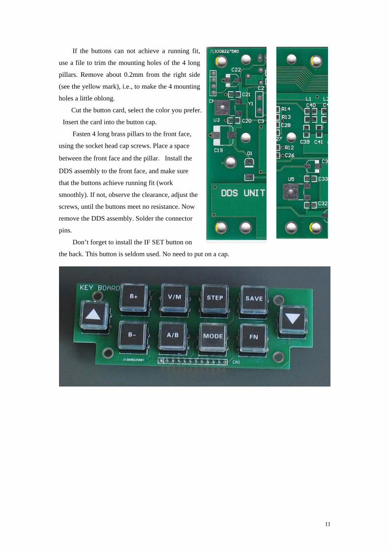
Construct DDS Assembly
Key board
Remove the 2 plastic pins on then
button back with pliers.
The clearance between the key and
the key opening in the front face is a
round 1mm. The PCB mounting holes
are manufactured with some clearance
so that the keys project through the key openings with suitable clearance on all sides.
Plug in the connecting pins. Install 3 shorter (10 mm) brass pillars. Fasten it to the DDS board.
10
If the buttons can not achieve a running fit,
use a file to trim the mounting holes of the 4 long
pillars. Remove about 0.2mm from the right side
(see the yellow mark), i.e., to make the 4 mounting
holes a little oblong.
Cut the button card, select the color you prefer.
Insert the card into the button cap.
Fasten 4 long brass pillars to the front face,
using the socket head cap screws. Place a space
between the front face and the pillar. Install the
DDS assembly to the front face, and make sure
that the buttons achieve running fit (work
smoothly). If not, observe the clearance, adjust the
screws, until the buttons meet no resistance. Now
remove the DDS assembly. Solder the connector
pins.
Don’t forget to install the IF SET button on
the back. This button is seldom used. No need to put on a cap.
11
Now, let’s move to SWITCH board construction.
12
Switch Board This board has only a few components. It is mounted to the back of the DDS board (Note: R2
is a 4.7K resistor.)
Definition of the
connectors.
CN1:External
power input
connector.
CN2:Battery
input connector.
CN3:Charging
connector.
Important! CN3
directly routes to
the external
power, and does not have current limiting device. This connector only suits the battery
pack with charging management. Insert a diode between the connector and the battery
charging port, if necessary, to prevent the current flow back.
CN4:Power supply output. The power to operate the rig is from this connector. Connect to
CN3 of PA with the heavy duty wires supplied with the kit. Turn the power switch to OFF
before plug in or disconnect external power.
13
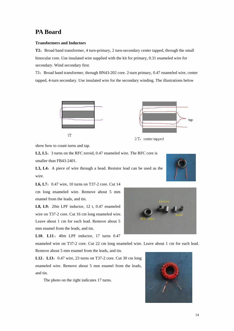
PA Board
Transformers and Inductors
T2:Broad band transformer, 4 turn-primary, 2 turn-secondary center tapped, through the small
binocular core. Use insulated wire supplied with the kit for primary, 0.31 enameled wire for
secondary. Wind secondary first.
T3:Broad band transformer, through BN43-202 core. 2-turn primary, 0.47 enameled wire, center
tapped, 4-turn secondary. Use insulated wire for the secondary winding. The illustrations below
show how to count turns and tap.
L2, L5:3 turns on the RFC toroid, 0.47 enameled wire. The RFC core is
smaller than FB43-2401.
L3, L4:A piece of wire through a bead. Resistor lead can be used as the
wire.
L6, L7:0.47 wire, 10 turns on T37-2 core. Cut 14
cm long enameled wire. Remove about 5 mm
enamel from the leads, and tin.
L8, L9:20m LPF inductor, 12 t, 0.47 enameled
wire on T37-2 core. Cut 16 cm long enameled wire.
Leave about 1 cm for each lead. Remove about 5
mm enamel from the leads, and tin.
L10, L11:40m LPF inductor, 17 turns 0.47
enameled wire on T37-2 core. Cut 22 cm long enameled wire. Leave about 1 cm for each lead.
Remove about 5 mm enamel from the leads, and tin.
L12、L13:0.47 wire, 23 turns on T37-2 core. Cut 30 cm long
enameled wire. Remove about 5 mm enamel from the leads,
and tin.
The photo on the right indicates 17 turns.
14
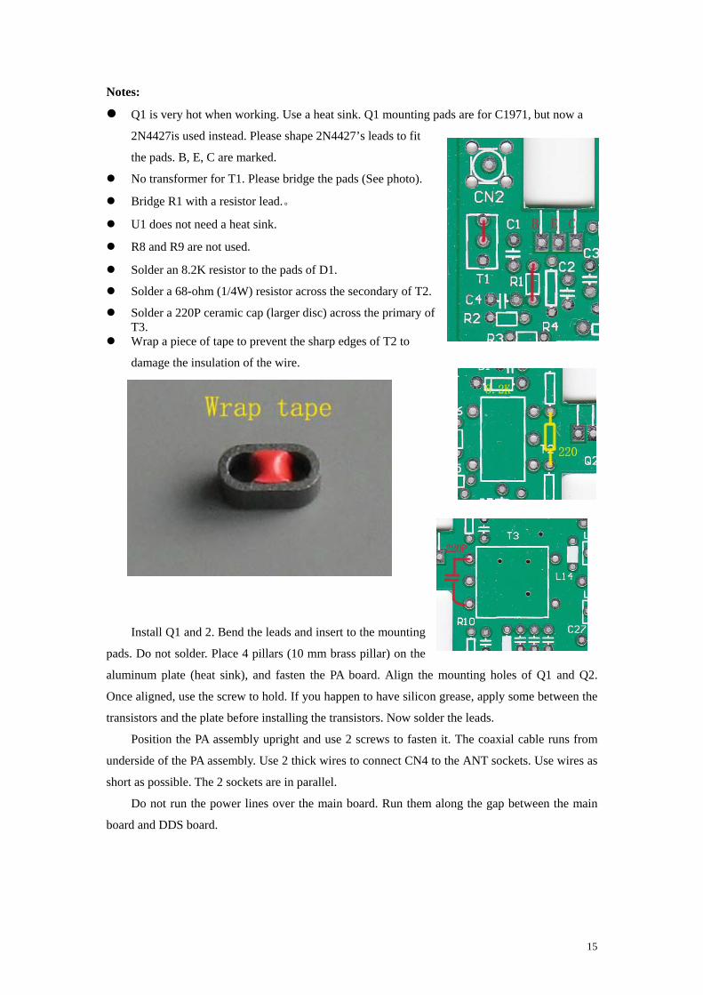
Notes:
Q1 is very hot when working. Use a heat sink. Q1 mounting pads are for C1971, but now a
2N4427is used instead. Please shape 2N4427’s leads to fit
the pads. B, E, C are marked. No transformer for T1. Please bridge the pads (See photo).
Bridge R1 with a resistor lead.。
U1 does not need a heat sink.
R8 and R9 are not used.
Solder an 8.2K resistor to the pads of D1.
Solder a 68-ohm (1/4W) resistor across the secondary of T2.
Solder a 220P ceramic cap (larger disc) across the primary of T3.
Wrap a piece of tape to prevent the sharp edges of T2 to
damage the insulation of the wire.
Install Q1 and 2. Bend the leads and insert to the mounting
pads. Do not solder. Place 4 pillars (10 mm brass pillar) on the
aluminum plate (heat sink), and fasten the PA board. Align the mounting holes of Q1 and Q2.
Once aligned, use the screw to hold. If you happen to have silicon grease, apply some between the
transistors and the plate before installing the transistors. Now solder the leads.
Position the PA assembly upright and use 2 screws to fasten it. The coaxial cable runs from
underside of the PA assembly. Use 2 thick wires to connect CN4 to the ANT sockets. Use wires as
short as possible. The 2 sockets are in parallel.
Do not run the power lines over the main board. Run them along the gap between the main
board and DDS board.
15
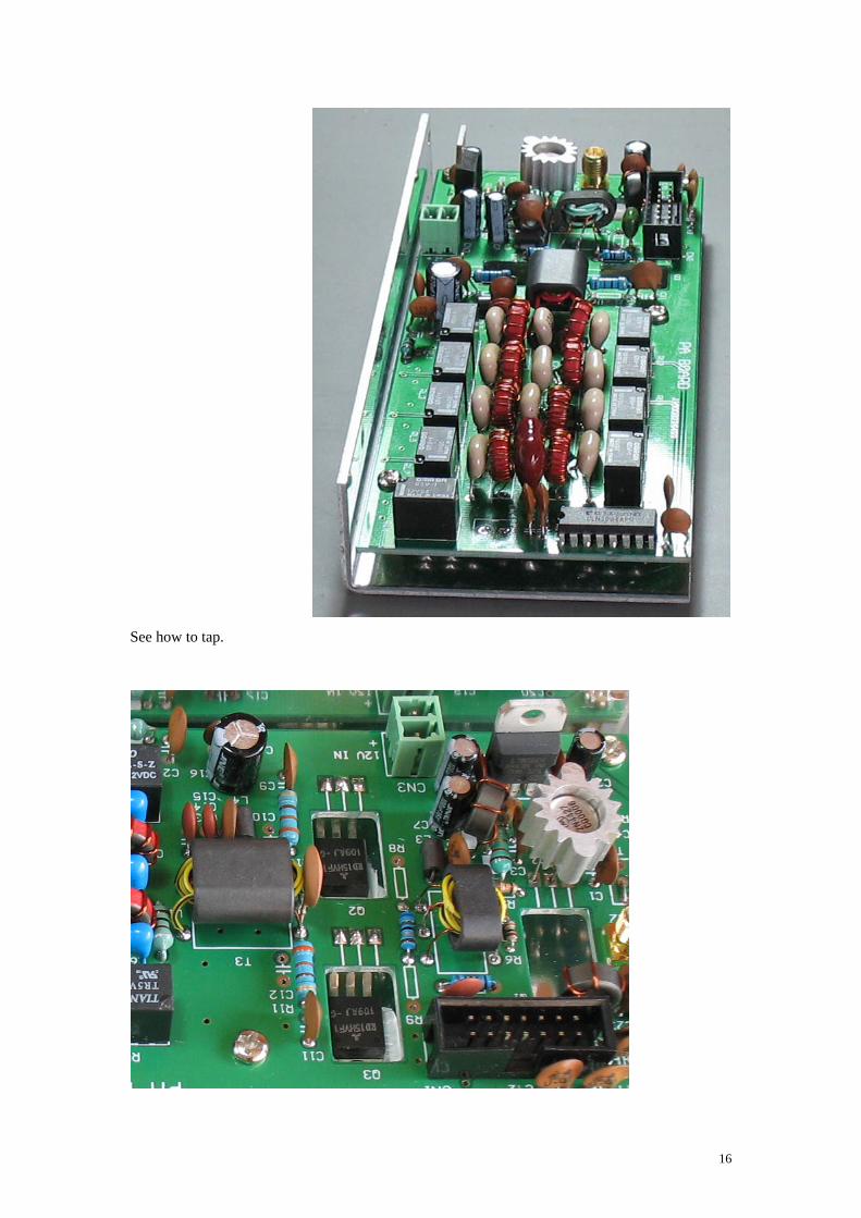
See how to tap.
16
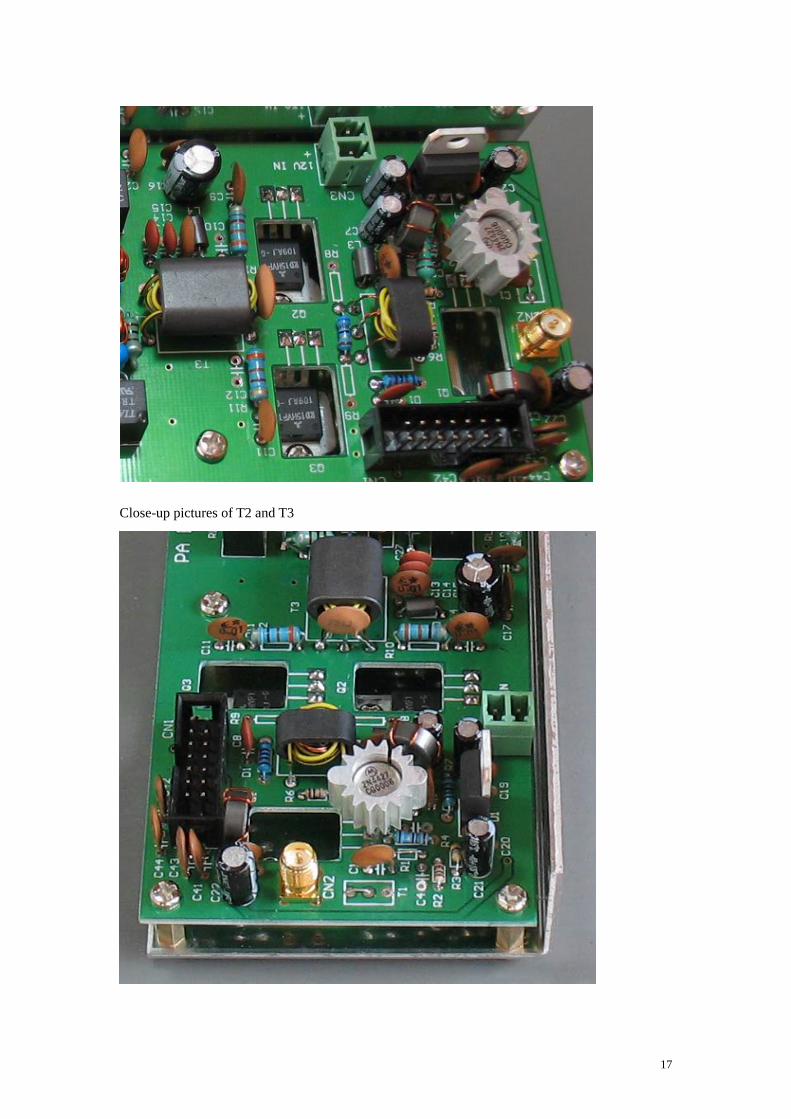
Close-up pictures of T2 and T3
17
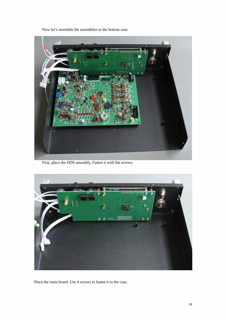
Now let’s assemble the assemblies to the bottom case.
First, place the DDS assembly. Fasten it with flat screws.
Place the main board. Use 4 screws to fasten it to the case.
18
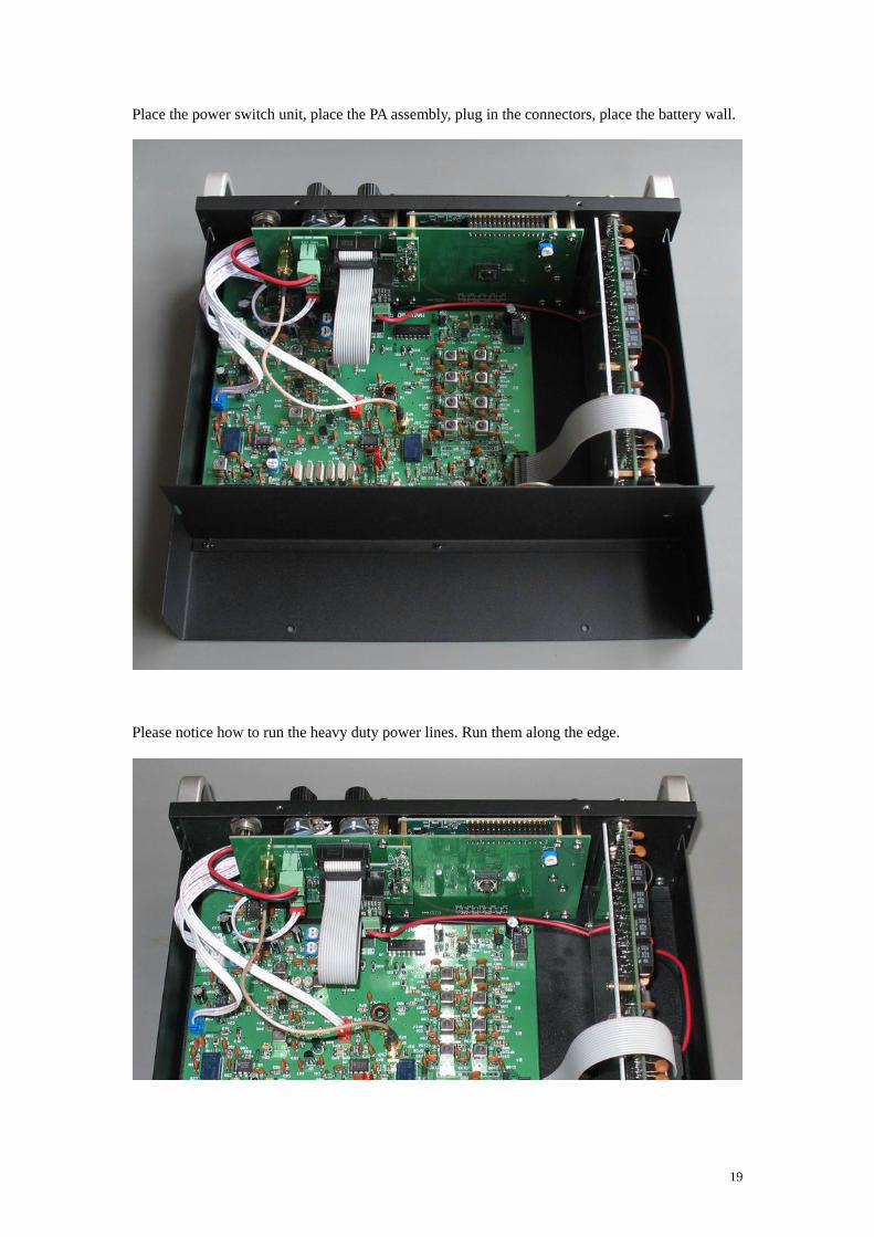
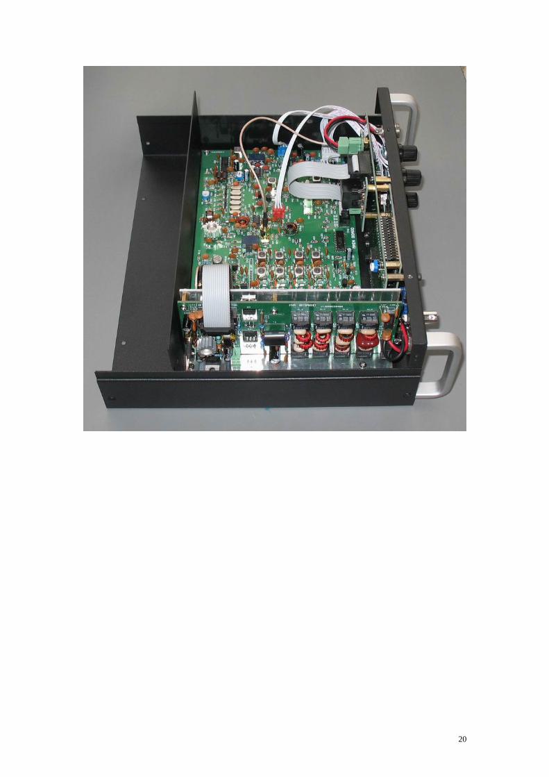
Place the power switch unit, place the PA assembly, plug in the connectors, place the battery wall.
Please notice how to run the heavy duty power lines. Run them along the edge.
19
20
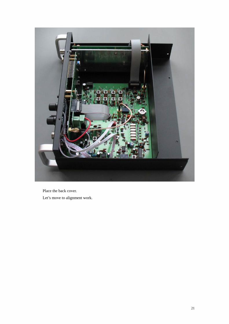
Place the back cover.
Let’s move to alignment work.
21
Alignment not very complicated. However, you need a frequency counter. Plug in
earphones, and antenna. Plug in power connector. Double check the polarity of the plug. Turn the
w
appear.
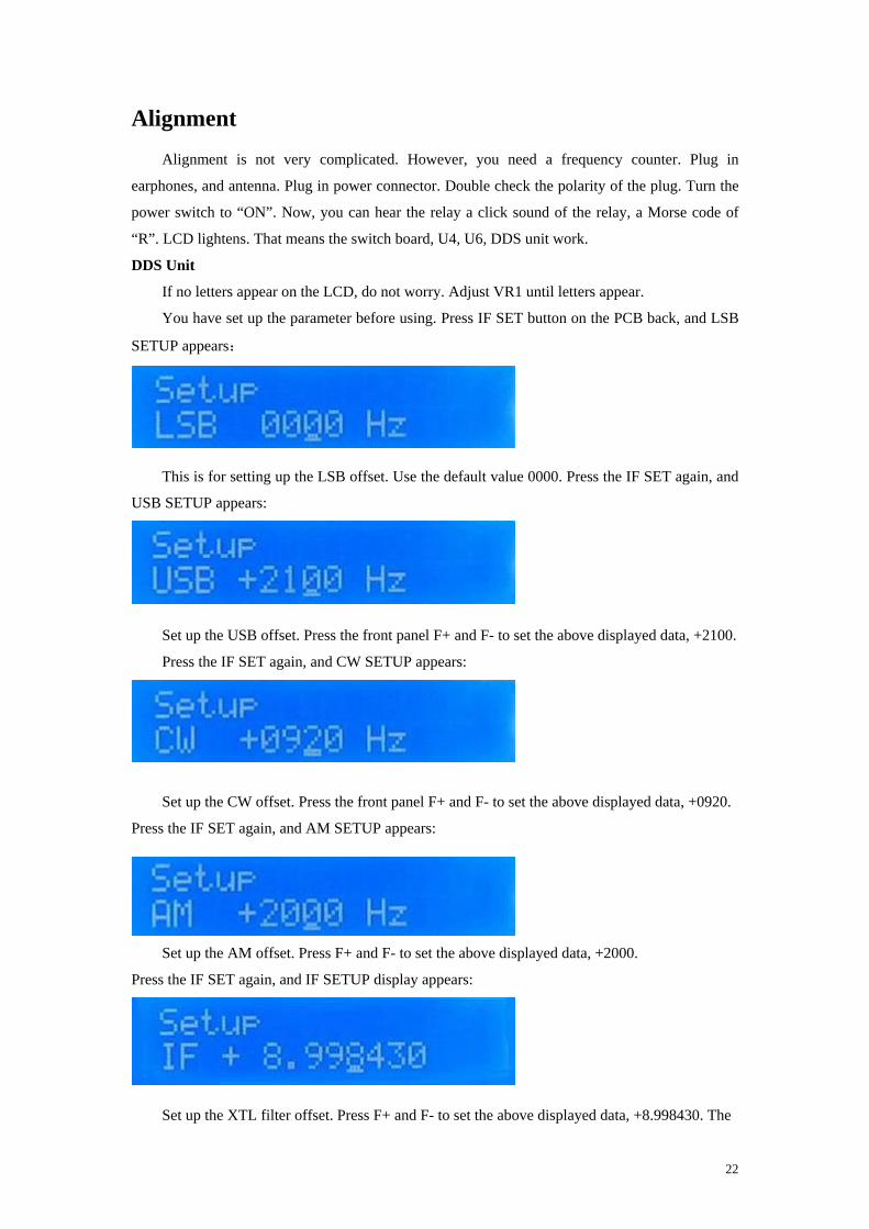
e set up the parameter before using. Press IF SET button on the PCB back, and LSB
SET
e 0000. ress the IF SET again, and
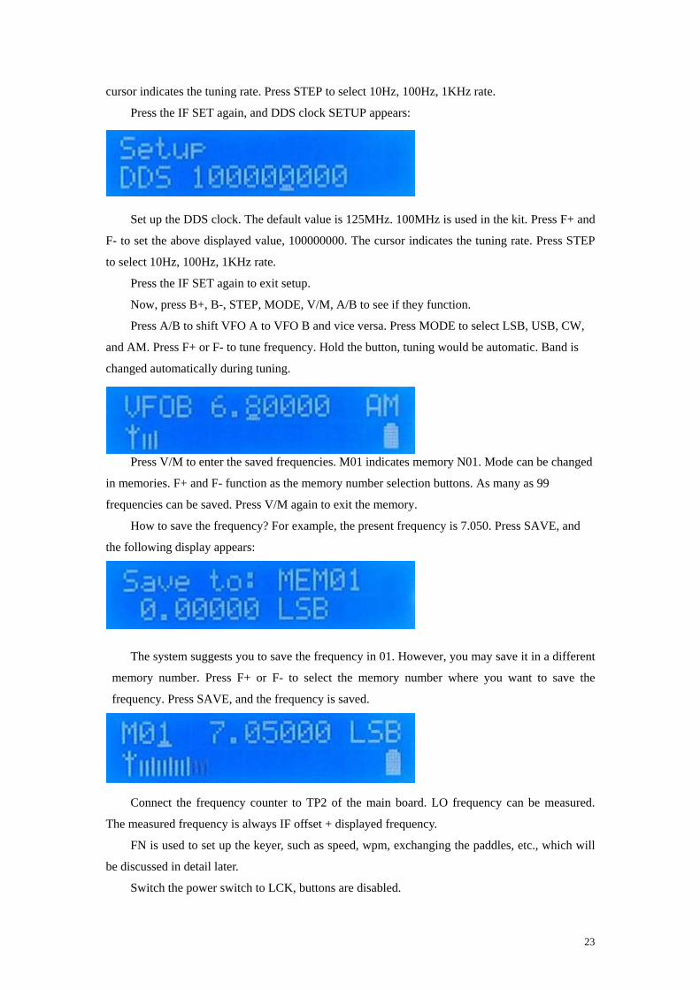
USB SETUP appears:
set the ove displayed data, +2100.
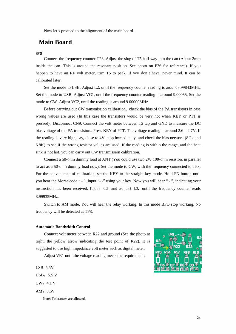
Press the IF SET again, and CW SETUP appears:
e above displayed data, +0920.
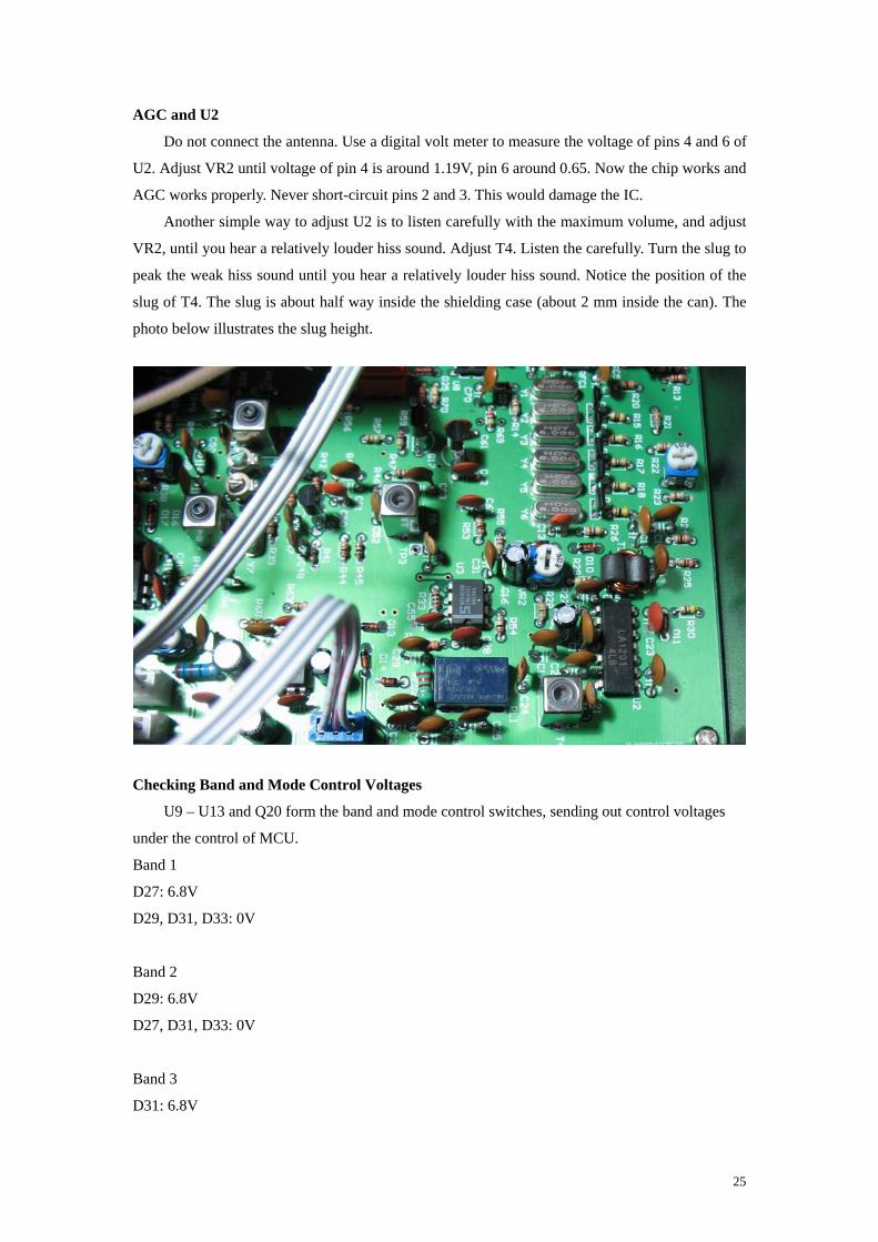
ess the IF SET again, and AM SETUP appears:
ed data, +2000.
Press the IF SET again, and IF SETUP display appears:
ve displayed data, +8.998430. The
Alignment is
po er switch to “ON”. Now, you can hear the relay a click sound of the relay, a Morse code of
“R”. LCD lightens. That means the switch board, U4, U6, DDS unit work.
DDS Unit
If no letters appear on the LCD, do not worry. Adjust VR1 until letters
You hav
UP appears:
This is for setting up the LSB offset. Use the default valu P
Set up the USB offset. Press the front panel F+ and F- to ab
Set up the CW offset. Press the front panel F+ and F- to set th
Pr
Set up the AM offset. Press F+ and F- to set the above display
Set up the XTL filter offset. Press F+ and F- to set the abo
22
cursor indicates the tuning rate. Press STEP to select 10Hz, 100Hz, 1KHz rate.
ress the IF SET again, and DDS clock SETUP appears:
MHz is sed in the kit. Press F+ and
F- to set the above displayed value, 100000000. The cursor indicate tuning rate. Press STEP
to select 10Hz, 100Hz, 1KHz rate.
O B and vice versa. Press MODE to select LSB, USB, CW,
and Hold the button, tuning would be automatic. Band is
chan
e ory N01. Mode can be changed
in memories. F+ and F- function as the memory number selectio ttons. As many as 99
frequencies can be saved. Press V/M again to exit the memory.
How to save the frequency? For example, the present frequ cy
e r, you may save it in a different
memory number. Press F+ or F- to select the memory number where you want to save the
frequency. Press SAVE, and the frequency is saved.
cy can be measured.
The measured frequency is always IF offset + displayed frequency.
FN is used to set up the keyer, such as speed, wpm, excha he paddles, etc., which will
be discussed in detail later.
P
Set up the DDS clock. The default value is 125MHz. 100 u
s the
Press the IF SET again to exit setup.
Now, press B+, B-, STEP, MODE, V/M, A/B to see if they function.
Press A/B to shift VFO A to VF
AM. Press F+ or F- to tune frequency.
ged automatically during tuning.
Press V/M to enter the saved frequencies. M01 indicates m m
n bu
en is 7.050. Press SAVE, and
the following display appears:
The system suggests you to save the frequency in 01. How ve
Connect the frequency counter to TP2 of the main board
Switch the power switch to LCK, buttons are disabled.
. LO frequen
nging t
23
Now let’s proceed to the alignment of the main board.
Main Board
BFO T5 half way into the can (About 2mm
insi around the resonant position. See photo on P26 for reference). If you
h volt meter, trim T5 to peak. If you don’t have, never mind. It can be
rated later.
g out CW transmission calibration, check the bias of the PA transistors in case
wron
ding is around 2.6 – 2.7V. If
hear “.-.”, indicating your
width Control
the test point of R22). It is
sugge o use high impedance volt meter such as digital meter.
reading meets the requirement:
CW:
AM:8.5V
lerances are allowed.
Connect the frequency counter TP3. Adjust the slug of
de the can. This is
appen to have an RF
calib
Set the mode to LSB. Adjust L2, until the frequency counter reading is around8.99843MHz.
Set the mode to USB. Adjust VC1, until the frequency counter reading is around 9.00055. Set the
mode to CW. Adjust VC2, until the reading is around 9.00000MHz.
Before carryin
g values are used (In this case the transistors would be very hot when KEY or PTT is
pressed). Disconnect CN9. Connect the volt meter between T2 tap and GND to measure the DC
bias voltage of the PA transistors. Press KEY of PTT. The voltage rea
the reading is very high, say, close to 4V, stop immediately, and check the bias network (8.2k and
6.8K) to see if the wrong resistor values are used. If the reading is within the range, and the heat
sink is not hot, you can carry out CW transmission calibration.
Connect a 50-ohm dummy load at ANT (You could use two 2W 100-ohm resistors in parallel
to act as a 50-ohm dummy load now). Set the mode to CW, with the frequency connected to TP3.
For the convenience of calibration, set the KEY to the straight key mode. Hold FN button until
you hear the Morse code “.-.”, input “-.-” using your key. Now you will
instruction has been received. Press KEY and adjust L3, until the frequency counter reads
8.99935MHz。
Switch to AM mode. You will hear the relay working. In this mode BFO stop working. No
frequency will be detected at TP3.
Automatic Band
Connect volt meter between R22 and ground (See the photo at
right, the yellow arrow indicating
sted t
Adjust VR1 until the voltage
LSB: 5.5V
USB:5.5 V
4.1 V
Note: To
24
AGC and U2
nnect the antenna. Use a digital volt meter to measure the voltage of pins 4 and 6 of
R2 until voltage of pin 4 is around 1.19V, pin 6 around 0.65. Now the chip works and
AG ort-circuit pins 2 and 3. This would damage the IC.
imple way to adjust U2 is to listen carefully with the maximum volume, and adjust
VR2
the can). The
phot
nd 1
D29
Do not co
U2. Adjust V
C works properly. Never sh
Another s
, until you hear a relatively louder hiss sound. Adjust T4. Listen the carefully. Turn the slug to
peak the weak hiss sound until you hear a relatively louder hiss sound. Notice the position of the
slug of T4. The slug is about half way inside the shielding case (about 2 mm inside
o below illustrates the slug height.
Checking Band and Mode Control Voltages
U9 – U13 and Q20 form the band and mode control switches, sending out control voltages
under the control of MCU.
Ba
D27: 6.8V
, D31, D33: 0V
Band 2
D29: 6.8V
D27, D31, D33: 0V
Band 3
D31: 6.8V
25
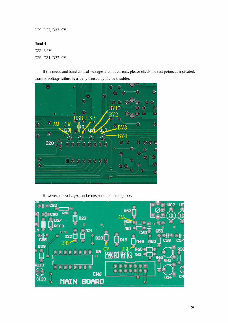
D29, D27, D33: 0V
Band 4
D33: 6.8V
D29, D31, D27: 0V
26
e mode and band control voltages are not correct, please check the test points as indicated.
tage failure is usually caused by the cold solder.
If th
Control vol
However, the voltages can be measured on the top side:
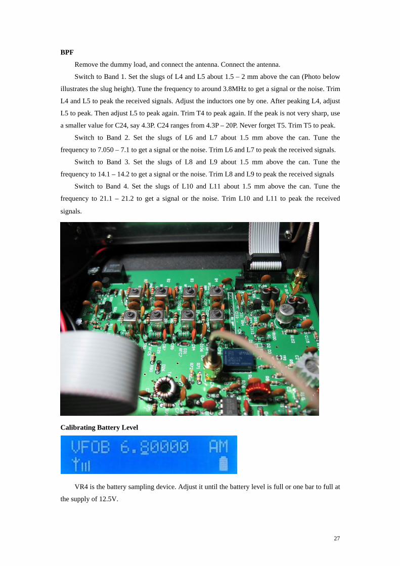
BPF emove the dummy load, and connect the antenna. Connect the antenna.
can (Photo below
illus
frequ
frequ
frequ
ttery level is full or one bar to full at
the s
R
Switch to Band 1. Set the slugs of L4 and L5 about 1.5 – 2 mm above the
trates the slug height). Tune the frequency to around 3.8MHz to get a signal or the noise. Trim
L4 and L5 to peak the received signals. Adjust the inductors one by one. After peaking L4, adjust
L5 to peak. Then adjust L5 to peak again. Trim T4 to peak again. If the peak is not very sharp, use
a smaller value for C24, say 4.3P. C24 ranges from 4.3P – 20P. Never forget T5. Trim T5 to peak.
Switch to Band 2. Set the slugs of L6 and L7 about 1.5 mm above the can. Tune the
ency to 7.050 – 7.1 to get a signal or the noise. Trim L6 and L7 to peak the received signals.
Switch to Band 3. Set the slugs of L8 and L9 about 1.5 mm above the can. Tune the
ency to 14.1 – 14.2 to get a signal or the noise. Trim L8 and L9 to peak the received signals
Switch to Band 4. Set the slugs of L10 and L11 about 1.5 mm above the can. Tune the
ency to 21.1 – 21.2 to get a signal or the noise. Trim L10 and L11 to peak the received
signals.
Calibrating Battery Level
VR4 is the battery sampling device. Adjust it until the ba
upply of 12.5V.
27
Calibrating S Meter
CD left corner represent the signal strength, each long bar representing 1S,
.,
ransmission
0-ohm dummy load.
e the frequency to 7.050, switch the mode to CW, with
POW
e microphone, LCD S meter bars also work, indicating
trans
e.
120(1uF)determines QSK delay. For full QSK, C120 is not necessary. In this case, the
16V could be used.
ic disc can be used.
distorted when very strong
eyer
has no backup battery. When the rig is turned off, all the settings of the keyer, such as
ee
The bars at the L
i.e S2 – S59+30dB. Receive a very strong signal, and adjust VR3 until all the bars appear.
T
Connect a 5
Let’s take 40m for example. Tun
ER to LOW POWER (Counter-clockwise to the end). Press the key, around 1W will be
measured. If you happen to have an oscilloscope, 20V p-p will be measured. Trim L6 and l7 to
peak. Now Increase the drive by PWR LEVEL, 18 – 20W will be obtained. Warning: If you use
two 2W 100-ohm resistor as the dummy load, do not use too much power. Or measure instantly.
Otherwise the resistors would be burned.
Switch to LSB, press PTT, speak to th
mission condition, and the output is around 18 – 20W at the HIGH power level.
If the output power is more than 20W, increase R72 to 470 ohms to reduce the driv QSK C
relays release as soon as the key is up. However, the TR relays have to withstand the frequent
switching. With C120 in position, there will be a short delay, i.e., the relay does not release at the
short key-up intervals to avoid the frequent relay contact motion.
Miscellaneous C122 -- Optional. A 470uF/
C121 -- absorbs interferences. 821 or 103 ceram
C24 -- This capacitor ranges from 4.3P – 20P. If the sound is a little
signal is tuned in, use a smaller value, say, 4.3P ceramic. The value is not very strict.
K
U6
sp d, WPM, call sign, etc. would not be remembered. Next you turn on the rig, keyer will be
loaded with the default values.
28
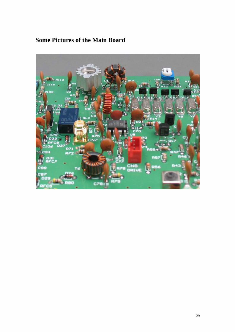
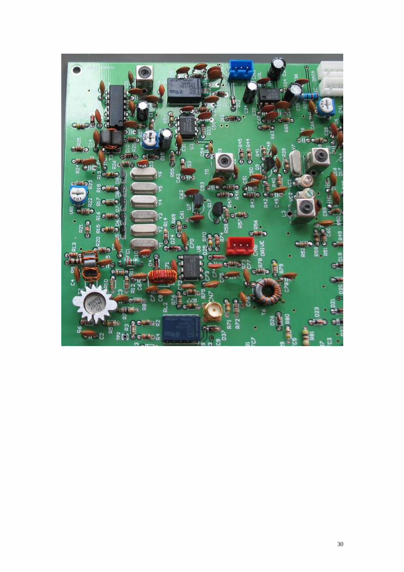
Some Pictures of the Main Board
29
30
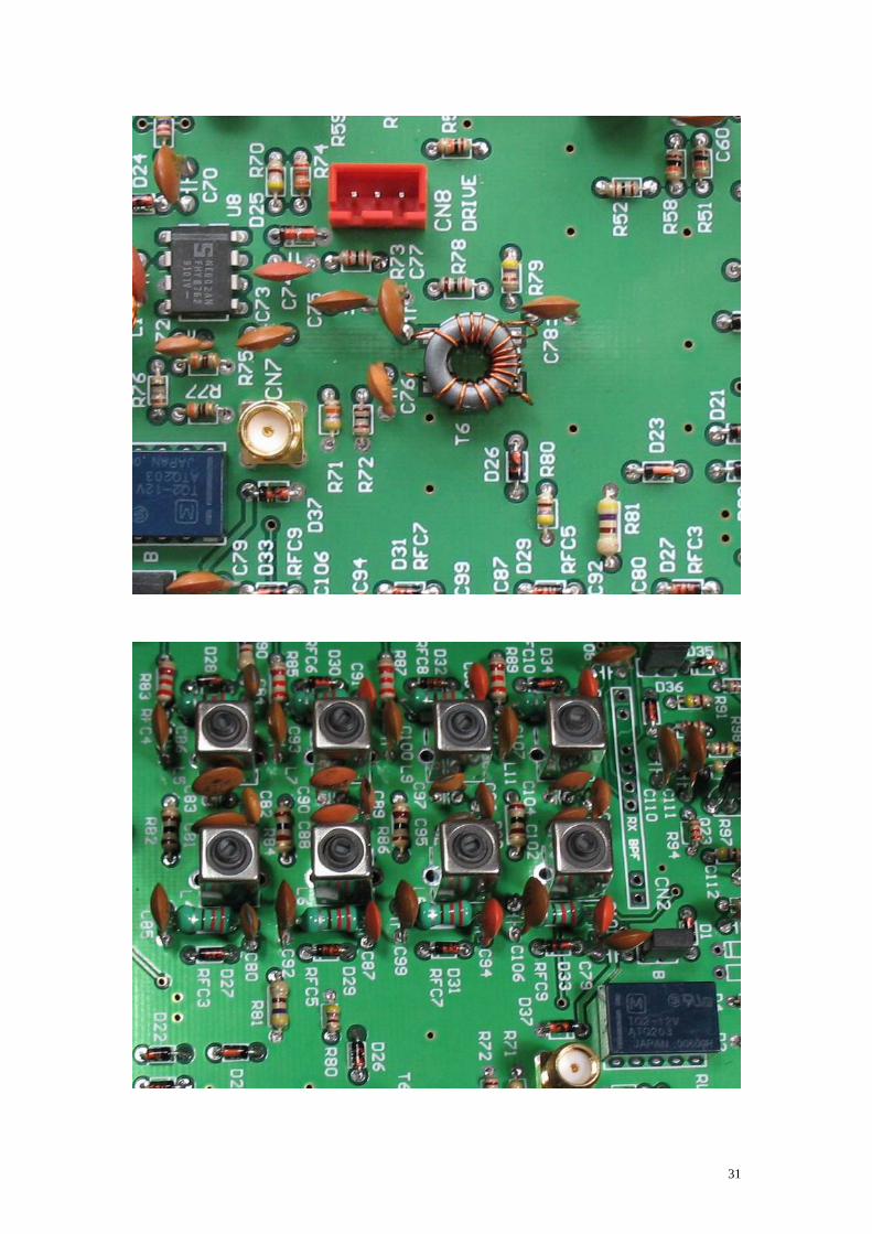
31
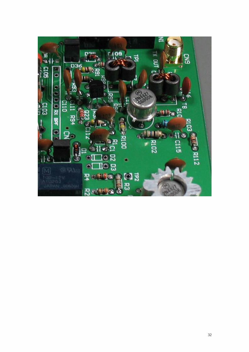
32
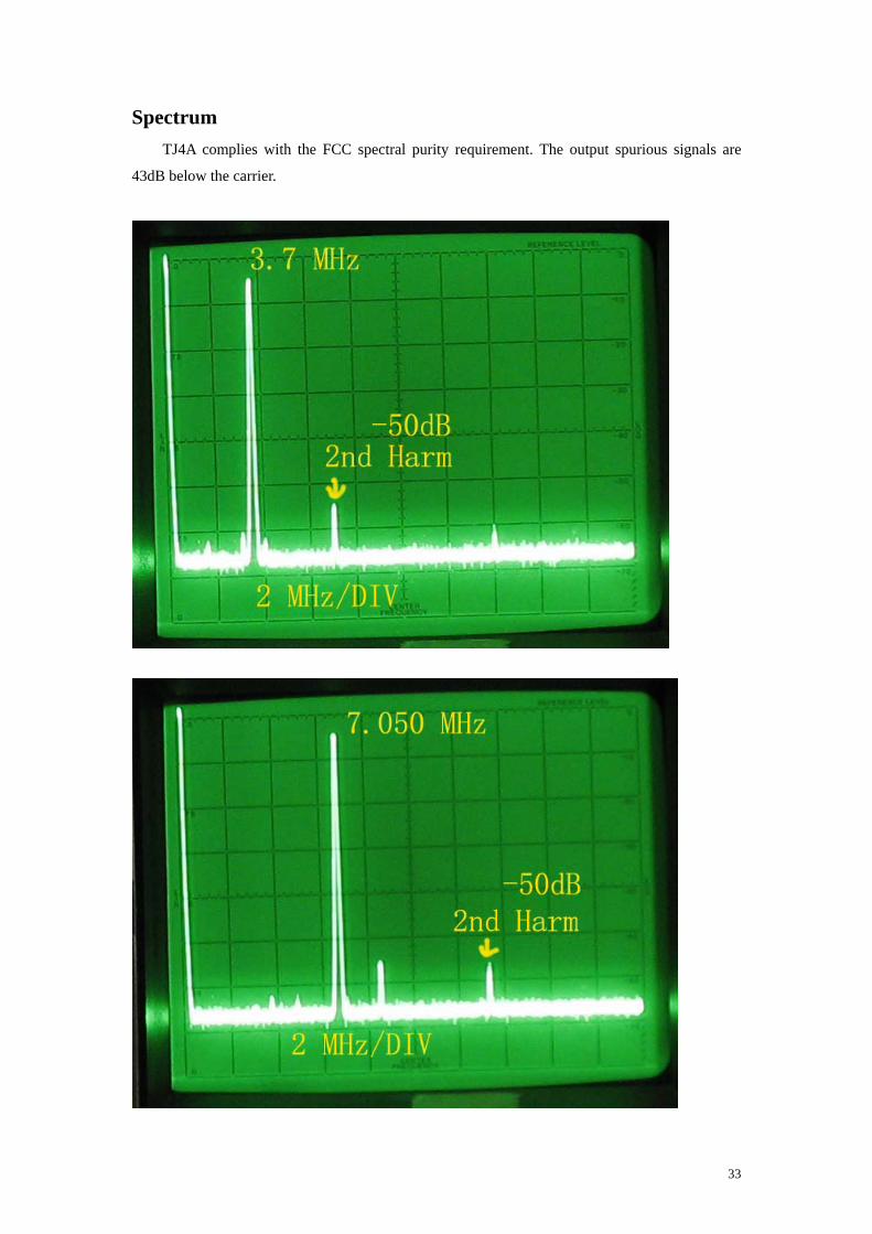
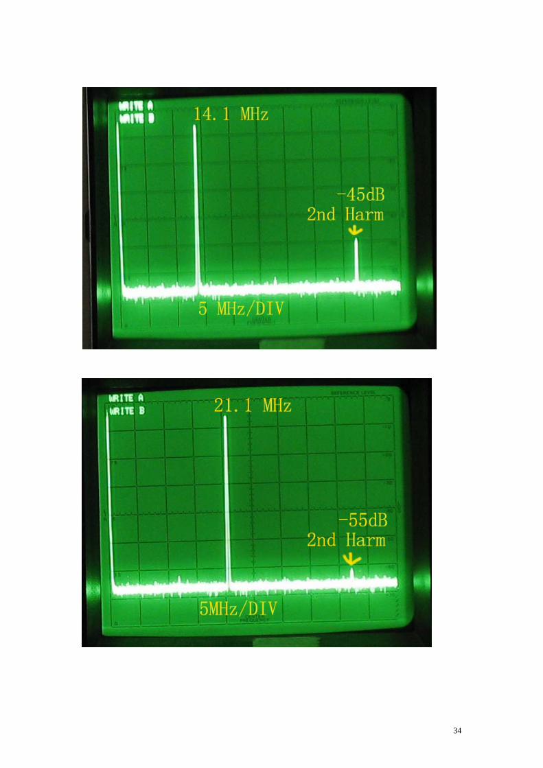
Spectrum TJ4A complies with the FCC spectral purity requirement. The output spurious signals are
43dB below the carrier.
33
34


![Suspended Metasurface Loaded Dual Band Dual Polarized ... › proceedings › procAP19 › papers2019 › PID5638363.pdf · filter. In [9], a dual band dual polarized antenna is](https://img.pdfslide.us/doc/110x75/5f14de5c84dbd949e06a47a4/suspended-metasurface-loaded-dual-band-dual-polarized-a-proceedings-a-procap19.jpg)