Embed Size (px)
Citation preview

September 2008 Altera Corporation Constraining and Analyzing Timing for External Mem
September 2008
Constraining and Analyzing Timing forExternal Memory Interfaces in Stratix IV,
Stratix III, and Cyclone III Devices
AN-438-4.0IntroductionEnsuring that your external memory interface meets the various timing requirements of today’s high-speed memory devices can be a challenge. Altera addresses this challenge by offering an external memory physical layer interface (PHY), the ALTMEMPHY megafunction, which employs a combination of source-synchronous and self-calibrating circuits to maximize system timing margin. This physical layer interface is a plug-and-play solution that is timing constrained and analyzed using the powerful Quartus® II TimeQuest Timing Analyzer. This PHY megafunction, along with the numerous device features offered by Stratix® IV, Stratix III, and Cyclone® III FPGAs, greatly simplifies the implementation of an external memory interface. All the information presented in this document for Stratix IV and Stratix III devices is applicable to HardCopy IV and HardCopy III devices, respectively.
This application note details the various timing paths that determine overall external memory interface performance, and describes the timing constraints and timing analyses used by the ALTMEMPHY megafunction to analyze these paths. Descriptions in this document are applicable to Stratix IV, Stratix III, and Cyclone III devices.
1 This application note focuses on timing constraints for ALTMEMPHY-based external memory interfaces. For information about timing constraints and analysis of external memory interfaces based on the ALTDQ_DQS megafunction and other source synchronous interfaces, refer to AN 433: Constraining and Analyzing Source Synchronous Interfaces. and the Quartus II TimeQuest Timing Analyzer chapter in volume 3 of the Quartus II Handbook.
1 This application note is not applicable to ALTMEMPHY memory interfaces implemented in Stratix II, Stratix II GX, or Arria® GX devices. For timing methodology information about these implementations, refer to AN 328: Interfacing DDR2 SDRAM with Stratix II, Stratix II GX, and Arria GX Devices.
Use this document in conjunction with the following literature:
■ AN 435: Using DDR and DDR2 SDRAM in Stratix III and Stratix IV Devices
■ AN 436: Using DDR3 SDRAM in Stratix III and Stratix IV Devices
■ AN 445: Design Guidelines for Implementing DDR and DDR2 SDRAM Interfaces in Cyclone III Devices
■ AN 461: Design Guidelines for Implementing QDRII+ and QDRII SRAM Interfaces in Stratix III Devices
■ External Memory Interfaces chapter of the Cyclone III Device Handbook
ory Interfaces in Stratix IV, Stratix III, and Cyclone III Devices

Page 2 Memory Interface Performance
■ External Memory Interfaces chapter of the Cyclone III Device Handbook
■ External Memory Interfaces chapter of the Stratix III Device Handbook
■ External Memory Interfaces chapter of the Stratix IV Device Handbook
Memory Interface PerformanceThe performance of an FPGA interface to an external memory device is dependent on the following:
■ Read data path timing
■ Write data path timing
■ Address/command path timing
■ Clock to strobe timing (tDQSS in DDR3/DDR2/DDR SDRAM, and tKHK#H in QDRII+/QDRII SRAM
■ Read resynchronization path timing (applicable for DDR3/DDR2/DDR SDRAM in Stratix IV and Stratix III devices)
■ Read postamble path timing (applicable for DDR3/DDR2/DDR SDRAM in Stratix IV and Stratix III devices)
■ PHY timing paths between IOE and core registers
■ PHY and controller internal timing paths (core fMAX and reset recovery/removal)
■ I/O toggle rate
■ Output clock specifications
1 External memory interface performance is dependent on various timing components, and overall system level performance is limited by performance of the slowest link (that is, the path with the smallest timing margins).
Constraining and Analyzing Timing for External Memory Interfaces in Stratix IV, Stratix III, and Cyclone III DevicesSeptember 2008 Altera Corporation

Memory Interface Performance Page 3
Figure 1 shows the external memory interface PHY for Stratix IV and Stratix III FPGAs.
Memory Interface Timing Components Memory interface timing components can be categorized into source-synchronous timing paths, calibrated timing paths, internal FPGA timing paths, and other FPGA timing parameters.
A closer look at all the register transfers occurring in the Stratix IV and Stratix III input data path reveals many source-synchronous and calibrated circuits. Figure 2 shows a block diagram of this input path with some of these paths identified. The output data path contains a similar set of circuits.
Figure 1. Stratix IV and Stratix III External Memory Interface PHY Block Diagram Notes (1), (2)
Notes to Figure 1:(1) This logical block diagram represents the Stratix IV and Stratix III external memory interface PHY interfacing with an SDRAM memory device.
While the DQ and DQS pins are bidirectional, this diagram represents separate signals for illustration purposes.(2) The blocks highlighted in blue are located inside the I/O element of each DQ/DQS pin.
DDR Outputand Output
Enable Registers
MemoryStratix IV FPGA
DLL
DDR Input Registers
Alignment & Synchronization
Registers
Half Data Rate Output Registers
Clock Management & Reset
4n 2nn
n
2n4n
DPRAM(2)
DQ (Read) (3)
DQ (Write) (3)
DQS Logic Block
DQS (Read) (3)
Half Data Rate Input Registers
2n
Half Data Rate Output Registers
4 2 DQS (Write) (3)
Resynchronization Clock
Alignment Clock
DQS Write Clock
Half-Rate Resynchronization
Clock
Half-Rate Clock
AlignmentRegisters
AlignmentRegisters
2n
2
DQ Write Clock
DQS EnableCircuit
PostambleControlCircuit
Postamble Enable
Postamble Clock
DDR Outputand Output
Enable Registers
September 2008 Altera Corporation Constraining and Analyzing Timing for External Memory Interfaces in Stratix IV, Stratix III, and Cyclone III Devices

Page 4 Memory Interface Performance
■ Source-synchronous paths
These are timing paths where clock and data signals are forwarded from the transmitting device to the receiving device.
An example of such a path is the FPGA-to-memory write data path. The FPGA device transmits DQ output data signals to the memory along with a center-aligned DQS output strobe signal. The memory device utilizes the DQS signal to clock the data on the DQ pins into its internal registers.
■ Calibrated paths
These are timing paths where the clock used to capture data is dynamically positioned within the data valid window (DVW) to maximize timing margin.
In Stratix IV and Stratix III FPGAs, the resynchronization of read data from the DQS-based capture registers to the FPGA system clock domain is implemented using a self-calibrating circuit. Upon initialization, the ALTMEMPHY megafunction’s sequencer block analyzes all path delays between the read capture and resynchronization registers to set up the resynchronization clock phase for optimal timing margin.
In Cyclone III FPGAs, the initial data capture from the memory device is performed by the ALTMEMPHY megafunction using a self-calibrating circuit. The DQS strobes from the memory are not used for capture. Instead, a dynamic PLL clock signal is used to capture DQ data signals into core LE registers.
Figure 2. Stratix IV and Stratix III Input Path Registers and Circuit Types in SDRAM Interface
DFF
I
DFF
Input Reg A
Input Reg B
neg_reg_out
I
DQ
DQ
DQS
DQ
Input Reg CI
DFF
DQ
DFF
DFF
DQ
DQ
DFF
DQ
DFF
DFF
DQ
DQ
DFF
DQ
I/O Clock Divider
Resynchronization Clock
Alignment &Synchronization
Registers
Double Data Rate Input Registers
Half Data Rate Registers
to core
to core
to core
to core
to core
Half-Rate Resynchronization Clock
FIFO in FPGA Core
Calibrated
I/O Source Synchronous
Internal Source Synchronous
Stratix IV or III FPGA SDRAM Memory
Constraining and Analyzing Timing for External Memory Interfaces in Stratix IV, Stratix III, and Cyclone III DevicesSeptember 2008 Altera Corporation

Memory Interface Performance Page 5
f For more details about calibrated circuits, refer to the Calibration section in the External DDR Memory PHY Interface Megafunction User Guide (ALTMEMPHY).
■ Internal FPGA timing paths
Other timing paths that impact memory interface timing include FPGA internal fM AX paths for PHY and controller logic. This timing analysis is common to all FPGA designs. With appropriate timing constraints on the design (such as clock settings), the TimeQuest Timing Analyzer reports the corresponding timing margins.
f For more information about the TimeQuest Timing Analyzer, refer to the Quartus II TimeQuest Timing Analyzer chapter in volume 3 of the Quartus II Handbook.
■ Other FPGA timing parameters
Certain FPGA data sheet parameters, such as I/O toggle rate and output clock specifications, can limit memory interface performance.
I/O toggle rates vary based on speed grade, loading, and I/O bank location— top/bottom versus left/right. The I/O pins on the top/bottom generally provide the highest toggle rates for SSTL and HSTL I/O standards due to their lower pin capacitance. This toggle rate is also a function of the termination used (OCT or external termination) and other settings such as drive strength and slew rate.
1 Be sure to check the I/O performance in the overall system performance calculation. The Quartus® II design software checks the toggle rate of all your I/O pins against your constraints during compilation and reports minimum pulse width violation warning messages as necessary.
Output clock specifications include clock period jitter, half-period jitter, cycle-to-cycle jitter, and skew between FPGA clock outputs (for example, skew between complementary clock outputs K and K# in QDRII and QDRII+ SRAM memory interfaces). These specifications can be obtained from the FPGA data sheet and the TimeQuest Timing Analyzer, and must meet memory device requirements. They are also used to determine the overall data valid window for signals transmitted between the memory and FPGA device.
September 2008 Altera Corporation Constraining and Analyzing Timing for External Memory Interfaces in Stratix IV, Stratix III, and Cyclone III Devices

Page 6 Memory Interface Performance
Stratix IV and Stratix III PHY Timing PathsTable 1 categorizes all Stratix IV and Stratix III external memory interface timing paths.
Cyclone III PHY Timing PathsTable 2 categorizes the various timing paths in a Cyclone III memory interface. Cyclone III devices use a calibrated PLL output clock for data capture and ignore the DQS strobe from the memory. Therefore, read resynchronization and postamble timing paths are not applicable to Cyclone III designs. The read capture is implemented in LE registers specially placed next to the data pin with fixed routing, and data is transferred from the capture clock domain to the system clock domain using a FIFO block. Figure 3 shows the Cyclone III input data path registers and circuit types.
Table 1. Stratix IV and Stratix III External Memory Interface Timing Paths (Note 1)
Timing Path Circuit Category Source Destination
Read Data (2) Source-Synchronous Memory DQ, DQS Pins DQ Capture Registers in IOE
Write Data (2) Source-Synchronous FPGA DQ, DQS Pins Memory DQ, DM, and DQS Pins
Address/Command (2) Source-Synchronous FPGA CK/CK# and Addr/Cmd Pins
Memory Input Pins
Clock-to-Strobe (2) Source-Synchronous FPGA CK/CK# and DQS Output Pins
Memory Input Pins
Read Resynchronization (2) Calibrated IOE Capture Registers IOE Alignment and Resynchronization Registers
Read Postamble Calibrated IOE Postamble Alignment Registers
IOE Postamble Registers
PHY IOE-Core Paths (2) Source-Synchronous IOE Half Data Rate Registers and Half-Rate Resynchronization Clock
FIFO in FPGA Core
PHY & Controller Internal Paths (2)
Internal Clock fMAX Core registers Core registers
I/O Toggle Rate I/O – Data sheet I/O Timing section
See the Maximum Input and Output Clock Toggle Rate section in the Stratix III Device Datasheet: DC and Switching Characteristics
FPGA Output Pin Memory Input Pins
Output Clock Specifications (Jitter, DCD)
I/O – Data sheet see the Switching Characteristics section in the Stratix III Device Datasheet: DC and Switching Characteristics
FPGA Output Pin Memory Input Pins
Notes to Table 1:
(1) Table 1 lists the timing paths applicable for an interface between Stratix IV and Stratix III devices and SDRAM memory devices.(2) Timing margins for this path are reported by the TimeQuest Timing Analyzer Report DDR function.
Constraining and Analyzing Timing for External Memory Interfaces in Stratix IV, Stratix III, and Cyclone III DevicesSeptember 2008 Altera Corporation

Memory Interface Performance Page 7
Understanding the nature of the timing path enables you to use an appropriate timing analysis methodology and constraints. The following section examines these aspects of memory interface timing paths.
Table 2. Cyclone III SDRAM External Memory Interface Timing Paths (Note 1)
Timing Path Circuit Category Source Destination
Read Data (2) Calibrated Memory DQ, DQS Pins DQ Capture Registers in LEs
Write Data (2) Source-Synchronous FPGA DQ, DQS Pins Memory DQ, DM, and DQS Pins
Address/Command (2) Source-Synchronous FPGA CK/CK# and Addr/Cmd Pins
Memory Input Pins
Clock-to-Strobe (2) Source-Synchronous FPGA CK/CK# and DQS Output Pins
Memory Input Pins
PHY Internal Timing (2) Internal Clock fMAX LE Half Data Rate Registers FIFO in FPGA Core
I/O Toggle Rate I/O – Data sheet I/O Timing section
FPGA Output Pin Memory Input Pins
Output Clock Specifications (Jitter, DCD)
I/O – Data sheetSwitching Characteristics section
FPGA Output Pin Memory Input Pins
Notes to Table 2:
(1) Table 2 lists the timing paths applicable for an interface between Cyclone III devices and SDRAM memory.(2) Timing margins for this path are reported by the TimeQuest Timing Analyzer Report DDR function.
Figure 3. Cyclone III Input Data Path Registers and Circuit Types in SDRAM Interface
Capture and Resynchronization Clock
FIFO
PLL
DQ
Cyclone III FPGA SDRAM MEMORY
Q
Q
D
D
Internal Source Synchronous
Calibrated
Q Q
Q
D D
D
Double Data Rate Input Registers
LE Register
LE Register
LE Register
September 2008 Altera Corporation Constraining and Analyzing Timing for External Memory Interfaces in Stratix IV, Stratix III, and Cyclone III Devices

Page 8 Timing Analysis Methodology for External Memory Interfaces
Timing Analysis Methodology for External Memory InterfacesThis section details the timing analysis methodology employed by the ALTMEMPHY megafunction for external timing paths between the FPGA and memory device, such as the read data and write data timing paths. Timing paths internal to the FPGA are either guaranteed by design and tested on silicon, or analyzed by the TimeQuest Timing Analyzer using corresponding timing constraints.
f For more details about the PHY, refer to the External DDR Memory PHY Interface Megafunction User Guide (ALTMEMPHY). For design guidelines about implementing and analyzing your external memory interface using the PHY in Stratix IV, Stratix III, or Cyclone III devices, refer to the following documents:
■ AN 435: Using DDR and DDR2 SDRAM in Stratix III and Stratix IV Devices
■ AN 436: Using DDR3 SDRAM in Stratix III and Stratix IV Devices
■ AN 445: Design Guidelines for Implementing DDR and DDR2 SDRAM Interfaces in Cyclone III Devices
■ AN 461: Design Guidelines for Implementing QDRII+ and QDRII SRAM Interfaces in Stratix III Devices
Timing Analysis MethodologyTiming margins for chip-to-chip data transfers can be defined as:
Margin = bit period – transmitter uncertainties – receiver requirements
Terminology:
■ Transmitter (TX) Channel-to-Channel Skew (TCCS) = sum of all TX uncertainties.
The timing difference between the fastest and slowest output edges on data signals, including tCO variation, clock skew, and jitter. The clock is included in the TCCS measurement and serves as the time reference.
■ Receiver (RX) Sampling Window (SW) requirement = sum of all RX requirements.
The period of time during which the data must be valid to capture it correctly. The setup and hold times determine the ideal strobe position within the sampling window.
■ Receiver Skew Margin (RSKM) = margin or slack at the receiver capture register.
f Refer to the DC and Switching Characteristics chapter of the Stratix IV Device Handbook, Stratix III Device Handbook, or Cyclone III Device Handbook for TCCS and SW specifications.
Constraining and Analyzing Timing for External Memory Interfaces in Stratix IV, Stratix III, and Cyclone III DevicesSeptember 2008 Altera Corporation

Timing Analysis Methodology for External Memory Interfaces Page 9
Figure 4 relates this terminology to a timing budget diagram.
The timing budget regions marked “½ × TCCS” represent the latest data valid time and earliest data invalid times. The region marked sampling window is the time required by the receiver during which data must stay stable. This sampling window is made up of the following:
■ Internal register setup and hold requirements
■ Skew on the data and clock nets within the receiver device
■ Jitter and uncertainty on the internal capture clock
1 Note that sampling window is not the capture margin or slack, but instead the requirement from the receiver. The margin available is denoted as RSKM.
The simple example illustrated in Figure 4 does not consider any board level uncertainties, assumes a center-aligned capture clock at the middle of the receiver sampling window region, and assumes an evenly distributed TCCS with respect to the transmitter clock pin. In this example, the left end of the bit period corresponds to time t = 0, and the right end of the bit period corresponds to time t = TUI (where TUI stands for time unit interval). Therefore, the center-aligned capture clock at the receiver is best placed at time t = TUI/2.
Therefore, the total margin = 2 × RSKM = TUI – TCCS – SW.
Consider the case where the clock is not center-aligned within the bit period (clock phase shift = P), and/or the transmitter uncertainties are unbalanced (TCCSLEAD
and TCCSLAG). TCCSLEAD is defined as the skew between the clock signal and latest data valid signal. TCCSLAG is defined as the skew between the clock signal and earliest data invalid signal. Also, the board level skew across data and clock traces are specified as tEXT. For this condition, you should compute independent setup and hold margins at the receiver (RSKMSETUP and RSKMHOLD). In this example, the sampling window requirement is split into a setup side requirement (SWSETUP) and hold side (SWHOLD) requirement. Figure 5 illustrates the timing budget for this condition. A timing budget similar to that shown in Figure 5 is used for Stratix IV and Stratix III FPGA read and write data timing paths.
Figure 4. Sample Timing Budget Diagram
½ × TCCS
Bit Period (TUI)
Setup + Hold + S kew + Jitter Data Skew with respect to Clock
Sampling Window (SW)
RSKM
RSKM
½ × TCCS
September 2008 Altera Corporation Constraining and Analyzing Timing for External Memory Interfaces in Stratix IV, Stratix III, and Cyclone III Devices

Page 10 Timing Analysis Methodology for External Memory Interfaces
Therefore, setup margin = RSKMSETUP = P – TCCSLEAD – SWSETUP – tEXT and hold margin = RSKMHOLD = (TUI – P) – TCCSLAG – SWHOLD – tEXT
The timing budget illustrated in Figure 4 with balanced timing parameters is applicable for calibrated paths where the clock is dynamically center-aligned within the data valid window. The timing budget illustrated in Figure 5 with unbalanced timing parameters is applicable for circuits that employ a static phase shift using a DLL or PLL to place the clock within the data valid window.
Read Data TimingMemory devices provide edge-aligned DQ and DQS outputs to the FPGA during read operations. The Stratix IV and Stratix III FPGAs center-aligns the DQS strobe using static DLL-based delays, and the Cyclone III FPGA uses a calibrated PLL clock output to capture the read data in LE registers without using DQS. While Stratix IV and Stratix III devices use a source synchronous circuit for data capture and Cyclone III devices use a calibrated circuit, the timing analysis methodology is quite similar, as shown in the following section.
Timing Analysis MethodologyWhen applying this methodology to read data timing, the memory device is the transmitter and the FPGA device is the receiver.
The transmitter channel-to-channel skew on outputs from the memory device can be obtained from the corresponding device data sheet. Let us examine the TCCS parameters for a DDR2 SDRAM device.
For DQS-based capture:
■ The time between DQS strobe and latest data valid is defined as tDQSQ
■ The time between earliest data invalid and next strobe is defined as tQHS
■ Based on earlier definitions, TCCSLEAD = tDQ SQ and TCCSLAG = tQHS
The sampling window at the receiver, the FPGA, includes several timing parameters:
■ Capture register micro setup and micro hold time requirements
■ DQS clock uncertainties due to DLL phase shift error and phase jitter
Figure 5. Sample Timing Budget with Unbalanced (TCCS and SW) Timing Parameters
TCCSLEAD
Bit Period (TUI)
Sampling Window (SW)
SWSETUP SWHOLD
RSKMSETUP
RSKMHOLD
TCCSLAG
Clock Phase Shift = P
tEXTtEXT
Constraining and Analyzing Timing for External Memory Interfaces in Stratix IV, Stratix III, and Cyclone III DevicesSeptember 2008 Altera Corporation

Timing Analysis Methodology for External Memory Interfaces Page 11
■ Clock skew across the DQS bus feeding DQ capture registers
■ Data skew on DQ paths from pin to input register including package skew
f Refer to the DC and Switching Characteristics chapter of the Stratix IV Device Handbook, the Stratix III Device Handbook, or the Cyclone III Device Handbook for TCCS and SW specifications.
Figure 6 shows the timing budget for a read data timing path.
Sample CalculationTable 3 details a read data timing analysis for a Stratix IV and Stratix III -2 speed grade device interfacing with a 400-MHz DDR2 SDRAM device.
Figure 6. Timing Budget for Read Data Timing Path
tDQSQ
Half-Period (min)
tSW_SETUP tSW_HOLD
DQ Skew + DQS Uncertainty + µTsu + µTh
Read Setup Margin
Read Hold Margin
tQHS
DQS Delay Shift
Duty Cycle Distortion (tDCD)
tEXT tEXT
Table 3. Read Data Timing Analysis for Stratix IV and Stratix III -2 Device with a 400-MHz DDR2 SDRAM (Part 1 of 2)
Parameter Specifications Value (ps) Description
Memory Specifications (1)
tHP 1250 Average half period as specified by the memory datasheet, tHP = 1/2 * tCK
tDCD 150 Duty cycle distortion = 2% × tCK + tJITdty = 0.02 × 2500 + 100 ps
tDQSQ 200 Skew between DQS and DQ from memory
tQHS 300 Data hold skew factor as specified by memory
FPGA Specifications (2)
tSW_SETUP 250 FPGA sampling window specifications for a given configuration (DLL mode, width, location, and so on.) tSW_HOLD 250
Board Specifications
tEXT 20 Maximum board trace variation allowed between any two signal traces (user specified parameter)
Timing Calculations
tDVW 560 tHP – tDCD – tDQSQ – tQHS – 2 × tEXT
tDQS_PHASE_DELAY 500 Ideal phase shift delay on DQS capture strobe
= (DLL phase resolution × number of delay stages × tCK) / 360° = (36° × 2 stages × 2500 ps)/360° = 500 ps
September 2008 Altera Corporation Constraining and Analyzing Timing for External Memory Interfaces in Stratix IV, Stratix III, and Cyclone III Devices

Page 12 Timing Analysis Methodology for External Memory Interfaces
Table 4 details a read data timing analysis for a Cyclone III -6 speed grade device interfacing with a DDR2 SDRAM device at 200 MHz using the SSTL18 Class I I/O standard and termination. A 267-MHz DDR2 SDRAM device is required to ensure positive timing margins for the 200-MHz memory interface clock frequency for the 200 MHz operation.
f For more information about DRAM device speed grade requirements, refer to AN 445: Design Guidelines for Implementing DDR and DDR2 SDRAM Interfaces in Cyclone III Devices.
Write Data TimingDuring write operations, the FPGA generates a DQS strobe and a center-aligned DQ data bus using multiple PLL driven clock outputs. These signals are received by the memory device and internally captured. The Stratix IV, Stratix III, and Cyclone III device families contain dedicated DDIO (double data rate I/O) blocks inside their I/O elements (IOE). The timing analysis for these device families on the write data path is identical.
Results Setup margin 30 RSKMSETUP = tDQSQ_PHASE_DELAY – tDQSQ – tSW_SETUP – tEXT
Hold margin 30 RSKMHOLD = tHP – tDCD – tDQS_PHASE_DELAY – tQHS – tSW_HOLD – tEXT
Notes to Table 3:
(1) This sample calculation uses memory timing parameters from a 72-bit wide 256-MB micron MT9HTF3272AY-80E 400-MHz DDR2 SDRAM DIMM.
(2) The sampling window specifications used in this sample calculation are obtained from the Stratix III FPGA data sheet for a -2 speed grade device and the 1.8-V SSTL I/O standard, and are preliminary until device characterization is complete.
Table 3. Read Data Timing Analysis for Stratix IV and Stratix III -2 Device with a 400-MHz DDR2 SDRAM (Part 2 of 2)
Parameter Specifications Value (ps) Description
Table 4. Read Data Timing Analysis for a 200-MHz DDR2 SDRAM on a Cyclone III -6 Speed Grade Device
Parameter SpecificationsValue (ps) Description
Memory Specifications
tHP 2500 Average half period as specified by the memory data sheet
tDCD 225 Duty cycle distortion = 2% × tCK + tJITdty = 0.02 × 5000 + 125 ps
tAC ± 500 Data (DQ) output access time for a 267-MHz DDR2 SDRAM device
FPGA Specifications
tSW_SETUP 580 FPGA sampling window specification for a given configuration (interface width, location, and so on). tSW_HOLD 550
Board Specifications
tEXT 20 Maximum board trace variation allowed between any two signal traces (user specified parameter)
Timing Calculations
tDVW 1235 tHP - tDCD - 2 × tAC – 2 × tEXT
Results Total margin 105 tDVW - tSW_SETUP - tSW_HOLD
Constraining and Analyzing Timing for External Memory Interfaces in Stratix IV, Stratix III, and Cyclone III DevicesSeptember 2008 Altera Corporation

Timing Analysis Methodology for External Memory Interfaces Page 13
Timing Analysis MethodologyFor write operations, the FPGA device is the transmitter and the memory device is the receiver. The memory device’s datasheet specifies data setup and data hold time requirements based on the input slew rate on the DQ/DQS pins. These requirements make up the memory sampling window, and include all timing uncertainties internal to the memory.
Output skew across the DQ and DQS output pins on the FPGA make up the TCCS specification. TCCS includes contributions from numerous internal FPGA circuits, including:
■ Location of the DQ and DQS output pins
■ Width of the DQ group
■ PLL clock uncertainties, including phase jitter between different output taps used to center-align DQS with respect to DQ
■ Clock skew across the DQ output pins, and between DQ and DQS output pins
■ Package skew on DQ and DQS output pins
f Refer to the DC and Switching Characteristics chapter of the Stratix IV Device Handbook, Stratix III Device Handbook, or Cyclone III Device Handbook for TCCS and SW specifications.
Figure 7 illustrates the timing budget for a write data timing path.
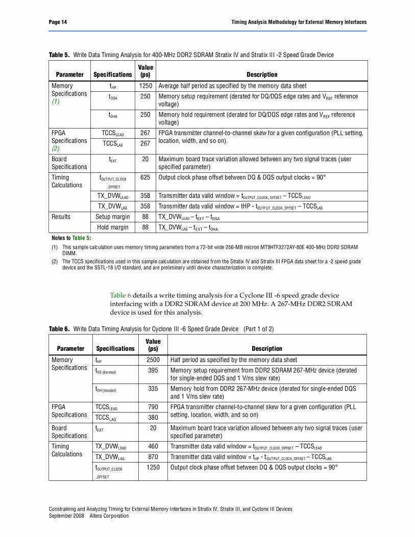
Sample CalculationTable 5 details a write data timing analysis for a Stratix IV and Stratix III -2 speed grade device interfacing with a DDR2 SDRAM device at 400 MHz. This timing analysis assumes the use of a differential DQS strobe with 2.0-V/ns edge rates on DQS, and 1.0-V/ns edge rate on DQ output pins. Consult your memory device’s data sheet for derated setup and hold requirements based on the DQ/DQS output edge rates from your FPGA.
Figure 7. Timing Budget for Write Data Timing Path
TCCSLEAD (DQS to late DQ)
Memory Sampling Window
tDS
Write Setup Margin
Write Hold Margin
TX_DVWLEAD
tEXTtEXT
TCCSLAG(early DQ to late DQS)
TX_DVWLAG
TCO /Clock skew
DQ-DQS Output Clock Offset
tDH
September 2008 Altera Corporation Constraining and Analyzing Timing for External Memory Interfaces in Stratix IV, Stratix III, and Cyclone III Devices
Page 14 Timing Analysis Methodology for External Memory Interfaces
.
Table 6 details a write timing analysis for a Cyclone III -6 speed grade device interfacing with a DDR2 SDRAM device at 200 MHz. A 267-MHz DDR2 SDRAM device is used for this analysis.
Table 5. Write Data Timing Analysis for 400-MHz DDR2 SDRAM Stratix IV and Stratix III -2 Speed Grade Device
Parameter SpecificationsValue (ps) Description
Memory Specifications (1)
tHP 1250 Average half period as specified by the memory data sheet
tDSA 250 Memory setup requirement (derated for DQ/DQS edge rates and VREF reference voltage)
tDHA 250 Memory hold requirement (derated for DQ/DQS edge rates and VREF reference voltage)
FPGA Specifications (2)
TCCSLEAD 267 FPGA transmitter channel-to-channel skew for a given configuration (PLL setting, location, width, and so on).TCCSLAG 267
Board Specifications
tEXT 20 Maximum board trace variation allowed between any two signal traces (user specified parameter)
Timing Calculations
tOUTPUT_CLOCK
_OFFSET
625 Output clock phase offset between DQ & DQS output clocks = 90°
TX_DVWLEAD 358 Transmitter data valid window = tOUTPUT_CLOCK_OFFSET – TCCSLEAD
TX_DVWLAG 358 Transmitter data valid window = tHP - tOUTPUT_CLOCK_OFFSET – TCCSLAG
Results Setup margin 88 TX_DVWLEAD – tEXT – tDSA
Hold margin 88 TX_DVWLAG – tEXT – tDHA
Notes to Table 5:
(1) This sample calculation uses memory timing parameters from a 72-bit wide 256-MB micron MT9HTF3272AY-80E 400-MHz DDR2 SDRAM DIMM.
(2) The TCCS specifications used in this sample calculation are obtained from the Stratix IV and Stratix III FPGA data sheet for a -2 speed grade device and the SSTL-18 I/O standard, and are preliminary until device characterization is complete.
Table 6. Write Data Timing Analysis for Cyclone III -6 Speed Grade Device (Part 1 of 2)
Parameter SpecificationsValue (ps) Description
Memory Specifications
tHP 2500 Half period as specified by the memory data sheet
tDS (derated) 395 Memory setup requirement from DDR2 SDRAM 267-MHz device (derated for single-ended DQS and 1 V/ns slew rate)
tDH (derated) 335 Memory hold from DDR2 267-MHz device (derated for single-ended DQS and 1 V/ns slew rate)
FPGA Specifications
TCCSLEAD 790 FPGA transmitter channel-to-channel skew for a given configuration (PLL setting, location, width, and so on)TCCSLAG 380
Board Specifications
tEXT 20 Maximum board trace variation allowed between any two signal traces (user specified parameter)
Timing Calculations
TX_DVWLEAD 460 Transmitter data valid window = tOUTPUT_CLOCK_OFFSET – TCCSLEAD
TX_DVWLAG 870 Transmitter data valid window = tHP - tOUTPUT_CLOCK_OFFSET – TCCSLAG
tOUTPUT_CLOCK
_OFFSET
1250 Output clock phase offset between DQ & DQS output clocks = 90°
Constraining and Analyzing Timing for External Memory Interfaces in Stratix IV, Stratix III, and Cyclone III DevicesSeptember 2008 Altera Corporation

Timing Constraints Used by the ALTMEMPHY Megafunction Page 15
Timing Constraints Used by the ALTMEMPHY MegafunctionTo ensure successful operation of your external memory interface, the ALTMEMPHY megafunction generates timing constraints for the PHY and the TimeQuest Timing Analyzer analyzes timing margins for the PHY. The timing constraints are generated while creating your custom megafunction variation and saved to an industry-standard Synopsys Design Constraints (SDC) file.
The SDC file is named <controller_variation_name>_phy_ddr_timing.sdc when the ALTMEMPHY megafunction is instantiated within the Altera® memory controller MegaCore®, and named <phy_variation_name>_ddr_timing.sdc when the ALTMEMPHY megafunction is instantiated stand-alone. You should add this SDC file to your Quartus II project. This allows the Quartus II Fitter to use timing driven compilation to optimize the timing margins. To add your SDC file, on the Assignments menu, click Settings. In the Settings dialog box, under Timing Analysis Settings, select TimeQuest Timing Analyzer and add the SDC file.
The timing margins for all ALTMEMPHY megafunction timing paths are analyzed by executing the Report DDR function in the TimeQuest Timing Analyzer, as described in the next section.
No timing constraints are required (or specified in the SDC file) for Stratix IV and Stratix III read capture and write data paths. This is because all DQ and DQS pins are pre-defined; the capture/output registers are built into the IOE, and signals use dedicated routing connections. No timing constraints are required for the Cyclone III read and write paths for similar reasons. Timing constraints have no impact on the read and write timing margins. However, the timing margins for these paths are analyzed using FPGA datasheet specifications and the user-specified memory data sheet parameters, as described in the next section.
The following SDC constraints are used by the ALTMEMPHY megafunction for internal FPGA timing paths, address/command paths, and clock-to-strobe timing paths. These include:
■ Creating clocks on PLL inputs.
■ Creating generated clocks using derive_pll_clocks. This includes all full-rate and half-rate PLL outputs, PLL reconfiguration clock, and I/O scan clocks.
■ Calling derive_clock_uncertainty.
■ Cutting timing paths for double-rate-rate I/O, calibrated paths, and most reset paths.
■ Setting output delays on address/command outputs (versus CK/CK# outputs).
■ Setting 2T or two clock-period multicycle setup for all half-rate address/command outputs, except nCS and ODT (versus CK/CK# outputs).
Results Setup margin 45 TX_DVWLEAD – tEXT – tDS
Hold margin 515 TX_DVWLAG – tEXT – tDH
Table 6. Write Data Timing Analysis for Cyclone III -6 Speed Grade Device (Part 2 of 2)
Parameter SpecificationsValue (ps) Description
September 2008 Altera Corporation Constraining and Analyzing Timing for External Memory Interfaces in Stratix IV, Stratix III, and Cyclone III Devices

Page 16 Timing Constraints Used by the ALTMEMPHY Megafunction
■ Setting output delays on DQS strobe outputs (versus CK/CK# outputs for DDR2 and DDR SDRAM)
As an example, timing constraints for address/command timing paths are described in detail. Similar constraints are generated for half-rate address/command timing paths as well as clock-to-strobe timing paths.
Address/Command Timing ConstraintsAddress/command signals are single data rate signals latched by the memory device using the FPGA output clock. Some of the address/command signals are half-data rate signals, while others, such as the chip select, are full-data rate.
The address/command timing paths are analyzed by the TimeQuest Timing Analyzer using the set_output_delay (max and min) constraints shown in the following example. For a Stratix IV and Stratix III memory interface with 400-MHz DDR2 SDRAM, the following constraints ensure address/command timing margin:
set_output_delay -add_delay -max -clock_fall -clock [get_clocks {avr_ddr2_phy_ddr_ck_mem_clk[0]}] 0.395 [get_ports mem_cs_n[0]]
set_output_delay -add_delay -min -clock_fall -clock [get_clocks {avr_ddr2_phy_ddr_ck_mem_clk[0]}] -0.395 [get_ports mem_cs_n[0]]
The set_output_delay -max value is computed as:
= Memory setup requirement + worst-case board skew between CK and address pins= tIS + tEXT = 0.375 + 0.020= 0.395 ns
The set_output_delay -min value is computed as:
= Memory hold requirement + worst-case board skew between CK and address pins= tIH + tEXT
= 0.375 + 0.020= 0.395 ns
The memory chip select pin, mem_cs_n[0], has a min and a max set_output_delay constraint with the CK memory clock pin, mem_clk[0]. Because memory clock output pins are differential, similar constraints exist for the chip select pin with respect to the CK# pin, mem_clk_n[0]. In DIMM interfaces that require three memory clock pairs, the chip select pin is constrained against all six mem_clk[]/mem_clk_n[] pins.
Constraining and Analyzing Timing for External Memory Interfaces in Stratix IV, Stratix III, and Cyclone III DevicesSeptember 2008 Altera Corporation

Timing Margin Report for the ALTMEMPHY Megafunction Page 17
Timing Margin Report for the ALTMEMPHY MegafunctionThe Report DDR task in the TimeQuest Timing Analyzer generates custom timing margin reports for all ALTMEMPHY instances in your design. This custom report is generated by the TimeQuest Timing Analyzer by sourcing the <variation>_report_timing.tcl script generated by the ALTMEMPHY MegaWizard® Plug-In Manager when the PHY was first instantiated.
1 ALTMEMPHY-based memory interface designs do not support the use of Report Data sheet timing specifications for analyzing margins on double-data rate I/O timing paths (read and write data paths). Instead, Report DDR must be used to perform I/O timing analysis with the TCCS and SW timing specifications described in the “Timing Analysis Methodology” on page 8. Report Datasheet results are based on the micro-timing model of the FPGA, and do not use the memory interface TCCS/SW specifications.
After compiling your design in the Quartus II software, launch the TimeQuest Timing Analyzer window and double-click Report DDR from the Tasks pane, as shown in Figure 8. This automatically executes the Create Timing Netlist, Read SDC File, and Update Timing Netlist tasks for your project.
The Report DDR feature creates a new DDR folder in the TimeQuest Timing Analyzer Report pane. Expanding the DDR folder reveals the detailed timing information for each PHY timing path, in addition to an overall timing margin summary for the ALTMEMPHY instance, as shown in Figure 9 and Figure 10.
Figure 8. Generating the Report DDR Timing Report in the TimeQuest Tasks Pane
September 2008 Altera Corporation Constraining and Analyzing Timing for External Memory Interfaces in Stratix IV, Stratix III, and Cyclone III Devices

Page 18 Timing Margin Report for the ALTMEMPHY Megafunction
Figure 9. DDR Timing Report in the TimeQuest Window Report Pane
Figure 10. Timing Margin Summary Window Generated by the Report DDR Task
Constraining and Analyzing Timing for External Memory Interfaces in Stratix IV, Stratix III, and Cyclone III DevicesSeptember 2008 Altera Corporation
Timing Closure in ALTMEMPHY Designs Page 19
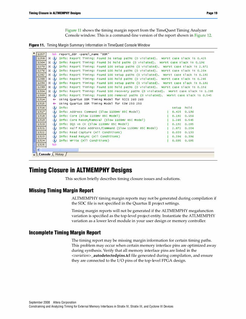
Figure 11 shows the timing margin report from the TimeQuest Timing Analyzer Console window. This is a command-line version of the report shown in Figure 12.
Timing Closure in ALTMEMPHY DesignsThis section briefly describes timing closure issues and solutions.
Missing Timing Margin ReportALTMEMPHY timing margin reports may not be generated during compilation if the SDC file is not specified in the Quartus II project settings.
Timing margin reports will not be generated if the ALTMEMPHY megafunction variation is specified as the top-level project entity. Instantiate the ATLMEMPHY variation as a lower level module in your user design or memory controller.
Incomplete Timing Margin ReportThe timing report may be missing margin information for certain timing paths. This problem may occur when certain memory interface pins are optimized away during synthesis. Verify that all memory interface pins are listed in the <variation>_autodetectedpins.tcl file generated during compilation, and ensure they are connected to the I/O pins of the top-level FPGA design.
Figure 11. Timing Margin Summary Information in TimeQuest Console Window
September 2008 Altera Corporation Constraining and Analyzing Timing for External Memory Interfaces in Stratix IV, Stratix III, and Cyclone III Devices

Page 20 Timing Closure in ALTMEMPHY Designs
Read Capture TimingIn Stratix IV and Stratix III devices, read capture timing may fail if the DQS phase shift selected is not optimal or if the board skew specified is large.
■ The effective DQS phase shift implemented by the DLL can be adjusted to balance setup and hold margins on the read timing path. The DQS phase shift can be adjusted in coarse PVT-compensated steps of 22.5°, 30°, 36°, or 45° by changing the number of delay buffers (range 1 to 4), or in fine steps using the DQS phase offset feature that supports uncompensated delay addition and subtraction in approximately 12 ps steps.
■ To adjust the coarse phase shift selection, determine the supported DLL modes for your chosen memory interface frequency by referencing the DLL and DQS Logic Block Specifications tables in the Switching Characteristics section of the device datasheet. For example, a 400 MHz DDR2 interface on a -2 speed grade device can use DLL mode 5 (resolution 36°, range 290 – 450 MHz) to implement a 72° phase shift, or DLL mode 6 (resolution 45°, range 360–560 MHz) to implement a 90° phase shift.
■ The phase_shift.tcl script and README files available for download with this application note can be used to adjust this DQS phase shift. Note that the script only supports phase shift adjustments for Stratix IV and Stratix III devices.
In Cyclone III devices, the read capture is implemented using a calibrated clock and therefore, no clock phase-shift adjustment is possible. Additionally, the capture registers are routed to specific LE registers in the LABs adjacent to the IOE using predefined routing. Therefore, no timing optimization is possible for this path. Ensure that the correct memory device speed grade is selected for the FPGA speed grade and interface frequency (as specified in AN 445: Design Guidelines for Implementing DDR and DDR2 SDRAM Interfaces in Cyclone III Devices).
1 Ensure that the appropriate board-skew parameter is specified in the ALTMEMPHY or the DDR3/DDR2/DDR SDRAM High-Performance Controller MegaWizard PHY settings page. The default board trace length mismatch used is 20 ps.
Write TimingNegative timing margins may be reported for write timing paths if the PLL phase shift used to generate the write data signals is not optimal. Adjust the PLL phase shift selection on the write clock PLL output using the PLL MegaWizard Plug-In Manager. Refer to the External DDR Memory PHY Interface Megafunction User Guide (ALTMEMPHY) to determine the PLL output counter tap used to generate the write clock.
1 Regenerating the ALTMEMPHY or Controller will overwrite changes made using the PLL MegaWizard Plug-In Manager.
Address/Command TimingTiming margins on the address/command timing path can be optimized by changing the PLL phase shift used to generate these signals. Modify the Dedicated Clock Phase setting in the PHY Settings page of the ALTMEMPHY or Controller MegaWizard Plug-In Manager.
Constraining and Analyzing Timing for External Memory Interfaces in Stratix IV, Stratix III, and Cyclone III DevicesSeptember 2008 Altera Corporation

Timing Closure in ALTMEMPHY Designs Page 21
Use the Pin Planner feature in the Quartus II software to accurately specify the board trace model information for all your address/command and memory clock output pins. The far-end load value and board trace delay differences between address/command and memory clock pins can result in timing failures if they are not accounted for during timing analysis.
Output delay chains on the address/command pins may not be optimally set by the Quartus II Fitter. To ensure that any PLL phase-shift adjustments are not negated by delay chain adjustments, create logic assignments using the Assignment Editor to set all address/command output pin D5 delay chains to 0.
Core Reset Recovery/RemovalA common cause for reset timing violations in ALTMEMPHY designs is the selection of a global or regional clock network for a reset signal. ALTMEMPHY does not require any dedicated clock networks for reset signals. Only ALTMEMPHY PLL outputs require clock networks, and any other PHY signal using clock networks may result in timing violations.
Such timing violations can be corrected by:
■ Setting the Global Signal logic assignment to Off for the problem path (via the Assignment Editor), or
■ Adjusting the logic placement (via the Assignment Editor or Chip Editor)
Clock-to-Strobe (for DDR and DDR2 SDRAM Only)Memory output clock signals and DQS strobes are generated using the same PLL output clock. Therefore, no timing optimization is possible for this path and positive timing margins are expected for interfaces running at or below the FPGA datasheet specifications.
For DDR3 interfaces, the timing margin for this path is reported as Write Leveling.
Read Resynchronization, Postamble, and Write Leveling Timing (for SDRAM Only)These timing paths are only applicable to Stratix IV and Stratix III devices, and are implemented using calibrated clock signals driving dedicated IOE registers. Therefore, no timing optimization is possible for these paths, and positive timing margin is expected for interfaces running at or below the FPGA datasheet specifications.
Ensure that the correct memory device timing parameters (tDQSCK, tDSS, tDSH) and board skew (tEXT) are specified in the ALTMEMPHY or High-Performance Controller MegaWizard Plug-In Manager.
September 2008 Altera Corporation Constraining and Analyzing Timing for External Memory Interfaces in Stratix IV, Stratix III, and Cyclone III Devices

Page 22 Timing Model Assumptions and Design Rules
Timing Model Assumptions and Design RulesALTMEMPHY-based memory interfaces are optimized for highest performance, and utilize a high-performance timing model to analyze calibrated and source-synchronous, double-data rate I/O timing paths. This timing model is applicable to designs that adhere to a set of predefined assumptions. These timing model assumptions include memory interface pin-placement requirements, PLL and clock network usage, I/O assignments (including I/O standard, termination, and slew rate), and many others.
For example, the read/write data path timing analysis is based on the FPGA pin-level tTCCS (transmitter channel-to-channel skew) and tSW (sampling window) specifications, respectively. While calculating the read and write timing margins, the Quartus II software analyzes the design to ensure that all read/write timing model assumptions listed below are valid for your ALTMEMPHY variation instance.
When the Report DDR task or report_timing.tcl script is executed, the timing analysis assumptions checker is invoked with specific ALTMEMPHY variation configuration information. If a particular design rule is not met, the Quartus II software will report the failing assumption as a Critical Warning message. See Figure 12 for a sample set of messages generated when the memory interface DQ, DQS, and CK/CK# pins are not placed in the same edge of the device.
The following section provides information about the timing model assumptions and design rules for all ALTMEMPHY-based memory interface designs.
Timing Assumptions Common to all Device FamiliesThis section documents timing analysis assumptions that are common to Stratix IV, Stratix III, and Cyclone III devices. The following sections document assumptions specific to each device family.
Figure 12. Read and Write Timing Analysis Assumption Verification
Constraining and Analyzing Timing for External Memory Interfaces in Stratix IV, Stratix III, and Cyclone III DevicesSeptember 2008 Altera Corporation

Timing Model Assumptions and Design Rules Page 23
Memory Clock Output AssumptionsTo verify the quality of the FPGA clock output to the memory device (CK/CK# or K/K#), which affects FPGA performance and quality of the read clock/strobe used to read data from the memory device, the following assumptions are needed:
■ The slew rate setting must be set to Fast or an on-chip termination (OCT) setting must be used.
■ The output delay chains must all be set to 0 (the default value applied by the Quartus II software). These delay chains include the Cyclone III output register to pin delay chain and the Stratix III D5 and D6 output delay chains.
■ The output open-drain parameter on the memory clock pin’s IO_OBUF atom must be set to Off. The Output Open Drain logic option must not be enabled.
■ The weak pull-up on the CK and CK# pads must be set to Off. The Weak Pull-Up Resistor logic option must not be enabled.
■ The Bus Hold on the CK and CK# pads must be set to Off. The Enable Bus-Hold Circuitry logic option must not be enabled.
■ All CK and CK# pins must be declared as output-only pins or bi-directional pins with the output enable set to VCC.
Write Data AssumptionsTo verify that the ALTMEMPHY-based memory interface can use the FPGA TCCS output timing specifications, the following assumptions are needed:
■ For QDRII, QDRII+, and RLDRAM II SIO memory interfaces, the write clock output pins (such as K/K# or DK/DK#) must be placed in DQS/DQSn pin pairs.
■ The PLL clock used to generate the write-clock signals and the PLL clock used to generate the write-data signals must come from the same PLL.
■ The slew rate for all write clocks and write data pins must be set to Fast or OCT must be used.
■ When auto deskew is not enabled (or not supported by the ALTMEMPHY configuration), the output delay chains and output enable delay chains must all be set to the default values applied by Quartus II. These delay chains include the Cyclone III output register and output enable register-to-pin delay chains, and the Stratix III D5 and D6 delay chains.
■ The output open drain for all write clocks and write data pins’ IO_OBUF atom must be set to Off. The Output Open Drain logic option must not be enabled.
■ The weak pull-up for all write clocks and write data pins must be set to Off. The Weak Pull-Up Resistor logic option must not be enabled.
■ The Bus Hold for all write clocks and write data pins must be set to Off. The Enable Bus-Hold Circuitry logic option must not be enabled.
September 2008 Altera Corporation Constraining and Analyzing Timing for External Memory Interfaces in Stratix IV, Stratix III, and Cyclone III Devices

Page 24 Timing Model Assumptions and Design Rules
Read Data AssumptionsTo verify that the ALTMEMPHY-based memory interface can use the FPGA Sampling Window (SW) input timing specifications, the following assumptions are needed:
■ For all memory types, the read clocks input pins must be placed on DQS pins (DQS/DQS# and QK/QK# inputs must be placed on differential DQS/DQSn pins on the FPGA, and the QDRII and QDRII+ SRAM CQ/CQ# inputs must be placed on CQ/CQn pins).
■ Read data pins (DQ/QVLD) must be placed on the DQ pins related to the selected DQS pins.
■ For QDRII SRAM interfaces, the complementary read clocks must have a single-ended I/O standard setting of HSTL-18 Class I or HSTL-15 Class I. For QDRII+ SRAM interfaces, the complementary read clocks should have a single-ended I/O standard of HSTL-15 Class I.
Mimic Path AssumptionsTo verify that the ALTMEMPHY-based DDR3/DDR2/DDR memory interface’s mimic path is configured correctly, the following assumption is needed:
■ The mimic path input must be placed on the mem_clk[0] pin.
Stratix IV- and Stratix III-Specific Assumptions
Memory Clock AssumptionsThe following memory clock assumptions are needed:
■ All memory clock output pins must be placed on DIFFOUT pin pairs.
■ In all DDR3 designs and DDR2 using differential DQS/DQS# strobes, (mem_clk[0] and mem_clk_n[0]) must be placed on DIFFIO_RX p- and n- pins for VT tracking using the mimic path. The remaining memory output clock pins (mem_clk[i] and mem_clk_n[i], where i = 1 or greater), can be placed on the DIFFOUT p- and n- pins.
■ For all other cases (including when the CK pin is a mimic pin, but the design does not use true differential DQS), the memory clock output pins must be placed on DIFFOUT p- and n- pins.
■ The CK output pin must be fed by DDIO output registers.
■ The CK# output pin must be fed by a signal splitter from its associated CK pin.
■ All memory clock pins must be placed on the same edge of the device (top, bottom, left, or right).
■ For DDR3 interfaces, the CK pins must be placed on FPGA output pins marked DQ, DQS, or DQSn.
■ For DDR3 interfaces, the CK pin must be fed by an OUTPUT_PHASE_ALIGNMENT WYSIWYG with a 0° phase shift.
■ For DDR3 interfaces, the PLL clock driving CK pins must be the same as the clock driving the DQS pins.
■ The T4 (DDIO_MUX) delay chains must be set to 2.
Constraining and Analyzing Timing for External Memory Interfaces in Stratix IV, Stratix III, and Cyclone III DevicesSeptember 2008 Altera Corporation

Timing Model Assumptions and Design Rules Page 25
■ The memory output clock signals must be generated with the DDIO configuration shown in Figure 13, with a signal splitter to generate the n- pin pair and a regional clock network-to-clock to output DDIO block.
Write Data AssumptionsTable 7 lists I/O standards supported for the write clock and write data signals for each memory type and pin location.
Figure 13. DIDO Configuration with Signal Splitter
Notes to Figure 13:(1) The mem_clk[0] and mem_clk_n[0] pins for DDR3, DDR2, and DDR SDRAM interfaces use the I/O input
buffer for feedback, therefore bidirectional I/O buffers are used for these pins. For memory interfaces using a differential DQS input, the input feedback buffer is configured as differential input; for memory interfaces using a single-ended DQS input, the input buffer is configured as a single-ended input. Using a single-ended input feedback buffer requires that the I/O standard’s VREF voltage is provided to that I/O bank’s VREF pins.
(2) Regional QCLK (quadrant) networks are required for memory output clock generation to minimize jitter.
Table 7. I/O standards (Part 1 of 2)
MemoryType Placement Legal I/O Standards for DQS Legal I/O Standards for DQ
DDR3 SDRAM Row I/O Differential 1.5-V SSTL Class I 1.5-V SSTL Class I
DDR3 SDRAM Column I/O Differential 1.5-V SSTL Class I
Differential 1.5-V SSTL Class II
1.5-V SSTL Class I
1.5-V SSTL Class II
DDR2 SDRAM Any SSTL-18 Class I
SSTL-18 Class II
Differential 1.8V SSTL Class I
Differential 1.8V SSTL Class II
SSTL-18 Class I
SSTL-18 Class II
DDR SDRAM Any SSTL-2 Class I
SSTL-2 Class II
SSTL-2 Class I
SSTL-2 Class II
QDRII SRAM Any Differential 1.5-V HSTL Class I
Differential 1.5-V HSTL Class II
Differential 1.8-V HSTL Class I
Differential 1.8-V HSTL Class II
1.5-V HSTL Class I
1.5-V HSTL Class II
1.8-V HSTL Class I
1.8-V HSTL Class II
QDRII+ SRAM Column I/O Differential 1.5-V HSTL Class I
Differential 1.5-V HSTL Class II
1.5-V HSTL Class I
1.5-V HSTL Class II
mem_clk (1)
QD
QD
System Clock (2)
FPGA LEs I/O Elements
VCC
mem_clk_n (1)
1
0
September 2008 Altera Corporation Constraining and Analyzing Timing for External Memory Interfaces in Stratix IV, Stratix III, and Cyclone III Devices

Page 26 Timing Model Assumptions and Design Rules
■ Differential write clock signals (DQS/DQSn) must be generated using the signal splitter.
■ The write data pins (DQ/DM/BWS#) must be placed in related DQ pins associated with the chosen DQS pin. The only exception to this rule is for QDRII and QDRII+ ×36 interfaces emulated using two ×18 DQ groups. For such interfaces, all of the write data pins must be placed on the same edge of the device (left, right, top, or bottom). Also, the write clock K/K# pin pair should be placed on one of the DQS/DQSn pin pairs on the same edge.
■ All write clock pins must have similar circuit structure.
■ For DDR3 interfaces, all DQS/DQS# write strobes must be fed by DDIO output registers clocked by the write-leveling delay chain in the OUTPUT_PHASE_ALIGNMENT block.
■ For non-DDR3 memory interfaces, all write clock pins must be fed by DDIO output registers clocked by a global or regional clock network.
■ All write data pins must have similar circuit structure.
■ For DDR3 interfaces, all write data pins must be fed by either DDIO output registers clocked by the OUTPUT_PHASE_ALIGNMENT block, VCC, or GND.
■ For non-DDR3 memory interfaces, all write data pins must be fed by either DDIO output registers clocked by a global or regional clock network, VCC, or GND.
■ The write clock output must be 72,° 90°, or 108° more than the write data output.
■ For DDR3 interfaces, the write-leveling delay chain in the OUTPUT_PHASE_ALIGNMENT block must implement a phase shift of 72°, 90°, or 108° to center-align write clock with write data.
■ For non-DDR3 memory interfaces, the phase shift of the PLL clock used to clock the write clocks must be 72 to 108° more than the PLL clock used to clock the write data clocks to generated center-aligned clock and data.
■ The T4 (DDIO_MUX) delay chains must all be set to 3. When differential DQS (using splitter) is used, T4 must be set to 2.
QDRII+ SRAM Row I/O Differential 1.5-V HSTL Class I 1.5-V HSTL Class I
RLDRAM II Any 1.8-V HSTL Class I
1.8-V HSTL Class II
Differential 1.5-V HSTL Class I
Differential 1.5-V HSTL Class II
1.8-V HSTL Class I
1.8-V HSTL Class II
1.5-V HSTL Class I
1.5-V HSTL Class II
Table 7. I/O standards (Part 2 of 2)
MemoryType Placement Legal I/O Standards for DQS Legal I/O Standards for DQ
Constraining and Analyzing Timing for External Memory Interfaces in Stratix IV, Stratix III, and Cyclone III DevicesSeptember 2008 Altera Corporation

Timing Model Assumptions and Design Rules Page 27
Read Data and Mimic Pin AssumptionsThe following read data and mimic-pin assumptions are needed:
■ For DDR3, DDR2, and DDR SDRAM interfaces, the read clock pin can only drive a DQS bus clocking a ×4 or ×9 DQ group.
■ For QDRII, QDRII+, and RLDARM II memory interfaces, the read clock pin can only drive a DQS bus clocking a ×9, ×18, or ×36 DQ group.
■ For non-hybrid interfaces, the mimic pin, all read clock, and all read data pins must be placed on the same edge of the device (top, bottom, left, or right). For hybrid interfaces, these pins can be placed on adjacent Row I/O and Column I/O edges and operate at reduced frequencies. Note that hybrid interfaces are not supported in Stratix IV devices (all interface pins must be placed on the same edge).
■ All read data pins and the mimic pin must feed DDIO_IN registers.
■ DQS phase-shift setting must be either 72° or 90° (supports only one phase shift for each operating band and memory standard).
■ All read clock pins must have the dqs_ctrl_latches_enable parameter of its DQS_DELAY_CHAIN WYSIWYG set to false.
■ The read data pins and mimic pin must have their input delay chains D1, D2, and D3 set to the Quartus II defaults.
■ The read clocks pins must have their D4 delay chain set to the Quartus II default value of 0.
■ The read data pins must have their T8 delay chain set to the Quartus II default value of 0.
DLL AssumptionsThe following DLL assumptions are needed:
■ The DLL must directly feed its delayctrlout[] outputs to all DQS pins without intervening logic or inversions.
■ The DLL must be in a valid frequency band of operation as defined in the corresponding device data sheet.
■ The DLL must have jitter reduction mode and dual-phase comparators enabled.
PLL and Clock Network AssumptionsTo verify that the memory interface’s PLL is configured correctly, the following assumptions are needed:
■ The PLL used to generate the memory output clock signals and write data/clock signals must be set to No compensation mode in Stratix IV and Stratix III devices to minimize output clock jitter.
■ The reference input clock signal to the PLL must be driven by the dedicated clock input pin located adjacent to the PLL, or from the clock output signal from the adjacent PLL. To minimize output clock jitter, the reference input clock pin must not be routed through the core using global or regional clock networks. If the reference clock is cascaded from another PLL, that upstream PLL must be configured in No compensation mode and Low bandwidth mode.
September 2008 Altera Corporation Constraining and Analyzing Timing for External Memory Interfaces in Stratix IV, Stratix III, and Cyclone III Devices

Page 28 Timing Model Assumptions and Design Rules
■ For DDR3 and DDR2 SDRAM interfaces, use only regional or dual-regional clock networks to route PLL outputs that are used to generate the write data, write clock, and memory output clock signals. This requirement ensures that the memory output clocks (CK/CK#) meet the memory device input clock jitter specifications, and that output timing variations or skew are minimized.
For other memory types, the same clock tree type (global, regional, or dual-regional) is recommended for PLL clocks generating the write clock, write data, and memory clock signals to minimize timing variations or skew between these outputs.
Mimic Pin AssumptionsTo verify that the VT tracking mimic path in ALTMEMPHY designs is set up correctly, the following assumptions are needed:
■ When differential DQS strobes are used (DDR3 and DDR2), the mimic pin must feed a true-differential input buffer. Placing the memory clock pin on a DIFFIO_RX pin pair allows the mimic path to track timing variations on the DQS input path.
■ When single-ended DQS strobes are used, the mimic pin must feed a single-ended input buffer.
Cyclone III-Specific AssumptionsThis section documents timing analysis assumptions that are specific to Cyclone III devices.
Memory Clock Assumptions■ The memory clock output pins must be placed on DIFFIO p- and n- pin pairs.
■ All memory clock output pins (CK/CK# or K/K#) must be fed by DDIO output registers.
■ The memory output clock signals must be generated using the DDIO configuration shown in Figure 14. In this configuration, the high register is strapped to VCC and the low register is strapped to GND.
Constraining and Analyzing Timing for External Memory Interfaces in Stratix IV, Stratix III, and Cyclone III DevicesSeptember 2008 Altera Corporation

Timing Model Assumptions and Design Rules Page 29
■ CK and CK# pins must be fed by a DDIO_OUT WYSIWYG with datainhi connected to GND.
■ CK and CK# pins must be fed by a DDIO_OUT WYSIWYG with datainlo connected to VCC.
■ CK or K pins must be fed by a DDIO_OUT with its clock input from the PLL inverted.
■ CK# or K# pins must be fed by a DDIO_OUT with its clock input from the PLL uninverted.
■ The I/O standard and current strength settings on the memory clock output pins must be as follows:
■ SSTL-2 Class I and 12 mA, or SSTL-2 Class II and 16 mA for DDR SDRAM interfaces
■ SSTL-18 Class I and 12 mA, or SSTL-18 Class II and 16 mA for DDR2 SDRAM interfaces
Write Data Assumptions■ Write data pins (DQ/DM/BWS#) must be placed on DQ pins related to the
selected DQS pins.
■ All write clock pins (DQS/DQS#) must be fed by DDIO output registers.
■ All write data pins must be fed by DDIO output registers, VCC, or GND.
■ The phase shift of the PLL clock used to generate the write clocks must be 72° to 108° more than the PLL clock used to generate the write data (nominally 90° offset).
■ The I/O standard and current strength settings on the write data- and clock-output pins must be as follows:
■ SSTL-2 Class I and 12 mA, or SSTL-2 Class II and 16 mA for DDR SDRAM interfaces
■ SSTL-18 Class I and 12 mA, or SSTL-18 Class II and 16 mA for DDR2 SDRAM interfaces
Figure 14. DDIO Configuration
DDIO
ClkCK or K
CK# or K#
PLL
VCC
DDIO
mem_clk_2xPLL reference clock
Clk
VCC
September 2008 Altera Corporation Constraining and Analyzing Timing for External Memory Interfaces in Stratix IV, Stratix III, and Cyclone III Devices

Page 30 Conclusion
Read Data and Mimic Input AssumptionsThe I/O standard setting on read data and clock input pins must be as follows:
■ SSTL-2 Class I and Class II for DDR SDRAM interface
■ SSTL-18 Class I and Class II for DDR2 SDRAM interfaces
■ The read data and mimic input registers (flipflops fed by the read data pin’s io_ibufs) must be placed in the LAB adjacent to the read data pin. A read data pin can have 0 input registers.
■ Specific routing lines from the IOE to core read data/mimic registers must be used. The Quartus II Fitter ensures proper routing unless user-defined placement constraints or LogicLock™ assignments force non-optimal routing. User assignments that prevent input registers from being placed in the LAB adjacent to the IOE must be removed.
■ The read data and mimic input pins’ input pad to core/register delay chain must be set to 0.
■ If all read data pins are on Row I/Os or Column I/Os, the mimic pin must be placed in the same type of I/O (Row I/O for read-data Row I/Os, Column I/O for read-data Column I/Os). For hybrid cases, the mimic pin can be placed anywhere.
PLL AssumptionsTo verify that the memory interface’s PLL is configured correctly, the following assumptions are needed:
■ The PLL used to generate the memory output clock signals and write data/clock signals must be set to normal compensation mode in Cyclone III devices.
■ The reference input clock signal to the PLL must be driven by the dedicated clock input pin located adjacent to the PLL. The reference input clock pin must not be routed through the core using global or regional clock networks to minimize output clock jitter. If the reference clock is cascaded from another PLL, that upstream PLL must be configured in Low Bandwidth mode.
ConclusionStratix IV, Stratix III, and Cyclone III devices greatly simplify the implementation of external memory interfaces using the new ALTMEMPHY megafunction. This physical layer interface is fully timing constrained with SDC constraints and timing analyzed using the ASIC-strength Quartus II TimeQuest Timing Analyzer. Maximize your overall memory interface performance and reliability by taking advantage of this plug-and-play interface.
Referenced Documents This application note references the following documents:
■ AN 433: Constraining and Analyzing Source Synchronous Interfaces
■ AN 435: Using DDR and DDR2 SDRAM in Stratix III and Stratix IV Devices
■ AN 436: Using DDR3 SDRAM in Stratix III and Stratix IV Devices
Constraining and Analyzing Timing for External Memory Interfaces in Stratix IV, Stratix III, and Cyclone III DevicesSeptember 2008 Altera Corporation

Document Revision History Page 31
■ AN 445: Design Guidelines for Implementing DDR and DDR2 SDRAM Interfaces in Cyclone III Devices
■ AN 461: Design Guidelines for Implementing QDRII+ and QDRII SRAM Interfaces in Stratix III Devices
■ Cyclone III Device Handbook
■ External DDR Memory PHY Interface Megafunction User Guide (ALTMEMPHY)
■ Quartus II TimeQuest Timing Analyzer chapter in volume 3 of the Quartus II Handbook
■ Stratix III Device Datasheet: DC and Switching Characteristics in volume 2 of the Stratix III Device Handbook
■ DC and Switching Characteristics of the Stratix IV Device Family in volume 4 of the Stratix IV Device Handbook
■ External Memory Interfaces chapter of the Cyclone III Device Handbook
■ Stratix III Device Handbook
■ Stratix IV Device Handbook
Document Revision HistoryTable 8 shows the revision history for this application note.
Table 8. Document Revision History
Date and Document Version Changes Made
Summary of Changes
September 2008 v4.0 Updated to include Stratix IV information. —
October 2007 v3.0 ■ Minor edits to Timing Analysis for External Memory Interfaces and Timing Constraints Used by the ALTMEMPHY Megafunction sections.
■ Updated Timing Margin Report for the ALTMEMPHY Megafunction section.
■ Added TimeQuest screen captures.
—
March 2007 v2.0 Updated to include Cyclone III information. —
February 2007 v1.0 Initial release —
September 2008 Altera Corporation Constraining and Analyzing Timing for External Memory Interfaces in Stratix IV, Stratix III, and Cyclone III Devices

Page 32 Document Revision History
101 Innovation DriveSan Jose, CA 95134www.altera.comTechnical Supportwww.altera.com/support
Copyright © 2008 Altera Corporation. All rights reserved. Altera, The Programmable Solutions Company, the stylized Altera logo, specific device designations, and all other words and logos that are identified as trademarks and/or service marks are, unless noted otherwise, the trademarks and service marks of Altera Corporation in the U.S. and other countries. All other product or service names are the property of their respective holders. Altera products are protected under numerous U.S. and foreign patents and pending applications, maskwork rights, and copyrights. Altera warrants performance of its semiconductor products to current specifications in accordance with Altera's standard warranty, but reserves the right to make changes to any products and services at any time without notice. Altera assumes no responsibility or liability arising out of the application or use of any information, product, or service described herein except as expressly agreed to in writing by Altera Corporation. Altera customers are advised to obtain the latest version of device specifications before relying on any published information and before placing orders for products or services.