Embed Size (px)
Citation preview
COUPLED QUANTUM – SCATTERING MODELING OF THERMOELECTRIC
PERFORMANCE OF NANOSTRUCTURED MATERIALS USING THE NON-
EQUILIBRIUM GREEN’S FUNCTION METHOD
By
Anuradha Bulusu
Dissertation
Submitted to the Faculty of the
Graduate School of Vanderbilt University
in partial fulfillment of the requirements
for the degree of
DOCTOR OF PHILOSOPHY
in
Interdisciplinary Materials Science
August, 2007
Nashville, Tennessee
Approved:
Professor D. G. Walker
Professor L. C. Feldman
Professor D. Li
Professor R. D. Schrimpf
Professor N. H. Tolk
Copyright © 2007 by Anuradha Bulusu
All Rights Reserved

Dedicated to my parents, Kameswari and Deekshatulu Bulusu
and my sisters Kanchana and Uma, for teaching me to never give up
iii
ACKNOWLEDGEMENTS
This research would not have been possible without the support of my advisor Prof. Greg Walker, a great
teacher and mentor. I am indebted to him for his excellent guidance and support and for the countless hours
he dedicated to our brain-storming sessions. He fostered a fun, stress-free working relationship while
continuing to encourage my academic progress making it a real pleasure to work for him.
I would like to thank my committee members for their genuine interest and support during the course of
this research. Their valuable advice and comments truly helped shape this research. I am grateful to Prof.
Supriyo Datta of Purdue University for providing us with a manuscript of his book on which much of this
research is based. I would also like to thank the National Science Foundation and a Vanderbilt Discovery
Grant for financial support of this research.
Special thanks are due to Sameer Mahajan and Dongyan Xu for their friendship and time spent discussing
various research problems. I would also like to thank Saumitra Vajandar and Sriram Dixit for their
friendship and support throughout my time in Nashville.
Finally, there is a very special person who deserves my deepest thanks. My husband Nandan has always
supported me and encouraged me through all the time spent working on this research. His caring and fun-
loving nature provided a welcome respite on many long days.
iv
TABLE OF CONTENTS DEDICATION…...…...……………………………………………………………………...........................iii
ACKNOWLEDGEMENTS ...........................................................................................................................iv
LIST OF FIGURES...................................................................................................................................... vii
Chapter
I. MOTIVATION ........................................................................................................................................1
Organization of the Thesis .................................................................................................................3 Background ........................................................................................................................................4 Bandstructure of Confined Electrons .................................................................................................7 Electron-Phonon Scattering................................................................................................................9
II. REVIEW OF THERMOELECTRIC MATERIALS AND MODELS...................................................12
Thermoelectric Properties ...............................................................................................................12 Development of Semiconductor Thermoelectric Materials ............................................................13 Development of Modeling of Thermoelectric Coefficients ............................................................18 Development of Low-Dimensional Models for Thermoelectric Applications................................30 Nanostructured Thermoelectric Materials.......................................................................................35
III. THE NEGF FORMALISM....................................................................................................................37
Numerical Scheme ..........................................................................................................................42 Calculation of Subband Currents ....................................................................................................43 Incorporating Electron-Phonon Scattering in the NEGF.................................................................45
IV. RESULTS FOR SILICON NANO-FILMS AND NANO-WIRES........................................................47
Effect of Electron Confinement on Seebeck Coefficient of Silicon Films and Wires ....................48 Effect of Electron Confinement on Electrical Conductivity of Silicon Films and Wires................52 Effect of Electron-Phonon Scattering on the Power Factor of Silicon Films..................................53
V. TRANSPORT IN SI/GE/SI QUANTUM WELL SUPERLATTICES ..................................................58
Effect of Substrate Strain ................................................................................................................59 Thermoelectric Properties of Strained Si/Ge/Si Quantum Well Superlattices ................................61 Effect of Electron-Phonon Scattering on the Power Factor of Si/Ge/Si Superlattices ....................70
VI. CONCLUSIONS....................................................................................................................................72 Appendix A. MATLAB PROGRAM FOR I-V CHARACTERISTICS OF SILICON FILMS...................................75 B. MATLAB PROGRAM FOR I-V CHARACTERISTICS OF SILICON WIRES ..................................80
v
C. MATLAB PROGRAM FOR I-V CHARACTERISTICS OF STRAINED SI/GE/SI SUPERLATTICES.......................................................................................................................................................................87 REFERENCES..............................................................................................................................................95
vi
LIST OF FIGURES
Figure 1. Bandstructure of silicon. .........................................................................................................................6 Figure 2. Constant energy surface ellipsoids for silicon and germanium...............................................................7 Figure 3. (a) 2D film with confinement along z axis (b) 1D wire with confinement along y and z axes. ..............7 Figure 4. (a) Bandstructure of a bulk solid (b) bandstructure of a confined solid with discrete energies along the z axis. ......................................................................................................................................8 Figure 5. Ratio of electron mobility to thermal conductivity of thermoelectric materials. Reproduced from data in [22]....................................................................................................................................15 Figure 6. Price’s doping curve for thermoelectric power. Reproduced from [52]................................................23 Figure 7. Distribution of density of states per unit volume with respect to energy of 3D , 2D and 1D structures ...............................................................................................................................................36 Figure 8. (a) Single energy level of an isolated channel (b) Broadening of electron energy levels in the channel when connected to contacts......................................................................................................38 Figure 9. Schematic diagram of 2D thin film and 1D wire with 1D and 2D confinement. ..................................41 Figure 10. Current density vs. thickness of silicon films doped to 1018cm-3 for (a) ballistic electron transport and (b) electron transport with longitudinal optical-phonon scattering................................48 Figure 11. Current-voltage characteristics of a ballistic silicon 6 nm film with doping of 5x1018cm-3. Applied temperature gradient ranges from 0K to 30K. .......................................................................49 Figure 12. Seebeck coefficient of ballistic silicon films and wires calculated using NEGF and compared to experiments [88, 89]........................................................................................................................50 Figure 13. Change in conduction band edge with doping for silicon ...................................................................50 Figure 14. Seebeck coefficients for 6nm and 12nm ballistic silicon films for high doping values ......................51 Figure 15. Predicted and measured [90] electrical conductivity values for a ballistic Silicon 6nm and 12nm film and 6 nmx6 nm wire....................................................................................................53 Figure 16. Comparison of subband energies for 6nm and 12nm silicon films .....................................................53 Figure 17. Comparison of the energy current with optical-phonon scattering, entering from the source and leaving through the drain for a 6nm film doped to 1018cm-3.........................................................54 Figure 18. Decrease in the electrical conductivity of a 12nm silicon film due to scattering with optical phonons. ..............................................................................................................................................55 Figure 19. Power factor of a 6nm film with and without optical-phonon scattering predicted using the NEGF formalism. ................................................................................................................................56
vii
Figure 20. Comparison of the electrical conductivity predictions between the NEGF model and the CRTA model [2, 77] for a 6 nm silicon film .......................................................................................57 Figure 21. Schematic representation of a Si/Ge/Si quantum well superlattice modeled in the simulation...........58 Figure 22. Schematic of a commercially grown Si/Ge/Si superlattice structure. .................................................59 Figure 23. Change in bandstructure of silicon and germanium with strain for Si(001) and Si0.5Ge0.5 substrates .............................................................................................................................................61 Figure 24. Seebeck coefficient vs. doping for Si/Ge/Si superlattice for various substrates compared with experimental measurements taken from [9, 98, 99, 100 and 101]. ..............................................62 Figure 25. Band diagram of quantum well for a doping of 1x1018cm-3 for Si(001) and Si0.5Ge0.5 substrates.......62 Figure 26. (a) Available Density of states vs. energy for 1x1018cm-3 doping of the superlattice (b) Density of states vs. energy for 5x1018cm-3 doping of superlattice. The red line in each case is the Fermi level ........................................................................................................................65 Figure 27. Electrical conductivity vs. doping for Si/Ge/Si superlattice for various substrates compared with measured values taken from [98, 99]..........................................................................................66 Figure 28. Power factor vs. doping of Si/Ge/Si superlattice for various substrates.............................................67 Figure 29. Power factor of Si/Ge/Si superlattices with Si (001) substrate for varying thickness of germanium layer..................................................................................................................................68 Figure 30. Power factor of Si/Ge/Si superlattices with Si0.5Ge0.5 substrate for varying thickness of the
germanium layer .........................................................................................................................................68 Figure 31. Comparison of subband energies of Si(2nm)/Ge2nm/Si(2nm) and Si(2nm)/Ge(4nm)/Si(2nm) superlattices on Si(001) and Si0.5Ge0.5 substrates. ...............................................................................69 Figure 32. Comparison of thermoelectric performance with scattering for strained Si(2nm)/Ge(1nm)/Si(2nm) superlattices with Si0.5Ge0.5 and Si(001) substrates.................................71
viii
CHAPTER I
MOTIVATION
Thermoelectric effects in materials allow for direct energy conversion in devices where thermal energy is
converted into electricity through the Seebeck effect. Similar energy conversion occurs when a current
passed through two dissimilar materials cools the junction through the Peltier effect. Applications of
thermoelectricity include chip level electronics cooling, power generators for remote telecommunication,
temperature control systems in solid state lasers etc. The emergence of low-cost, high-efficiency
thermoelectric power generators will also help reduce our dependence on non-renewable energy resources.
Widespread commercial applications of thermoelectrics have been limited by their low efficiency which is
characterized by the dimensionless thermoelectric figure of merit ZT = S2σT/κ where S is the Seebeck
coefficient, σ is the electrical conductivity and κ is the thermal conductivity [1]. The Seebeck coefficient
and electrical conductivity depend only on the electronic properties of the material while the thermal
conductivity can be dominated by contributions from both the electronic component as well as lattice
vibrations. The best commercially available thermoelectric materials have ZT ≈ 0.9. Extensive research has
been focused towards developing materials that have a high Seebeck coefficient as well as structures that
will either have reduced thermal conductivity or enhanced electrical conductivity resulting in an increase in
ZT.
The advent of quantum well nanofilm and nanowire superlattice structures that improve the value of ZT due
to a number of advantages shifted the focus from bulk materials towards understanding carrier transport
behavior in nanostructures. Quantum confinement in nanostructures increases the local carrier density of
states per unit volume near the Fermi energy increasing the Seebeck coefficient [2] while the thermal
conductivity can be decreased due to phonon confinement [3, 4] and phonon scattering at the material
interfaces in the superlattices [4, 5, 6]. Normally, the electrical conductivity is assumed not to be
1
significantly affected due to the large semiconductor bandgap and the disparity between the electron and
phonon mean free paths [7, 8]. The combined benefits of reduced thermal conductivity and improved
Seebeck coefficient imply a theoretically higher ZT compared to the bulk structures. However,
experimental observations especially in the case of Si/Ge superlattices have not been able to achieve the
presumed benefits of superlattice thermoelectric devices despite theoretically predicted improvements in ZT
and experimentally observed reduction in the thermal conductivity of superlattices compared to their bulk
counterparts [2, 9]. Hence there is a need to better understand the effect of all the significant factors
contributing to the thermoelectric figure of merit of nanoscale devices. In this regard, the two main
phenomena that affect electron transport in nanostructures are 1) electron confinement and 2) electron
scattering effects such as electron-phonon scattering, electron-impurity scattering etc.
The most common method of predicting thermoelectric parameters is based on a semi-classical, relaxation
time approximation model where the system is assumed to be only slightly perturbed from equilibrium.
While the semi-classical models work well in predicting the performance of materials in the bulk regime,
wave effects that can not be captured naturally in particle-based models begin to dominate in
nanostructured materials. Reduced dimensionality results in electron confinement and the formation of
discrete subband energy levels in the confined direction. Tunneling of electrons and diffraction,
characteristic of wave behavior, begin to dominate at low dimensions. Reduced dimensionality also results
in phonon confinement and formation of phonon bandgaps that changes their dispersion relation. Although
most of these models use confined dispersion relations, transport and thermoelectric coefficients are still
calculated using the semi-classical relaxation time approximation model that cannot adequately capture
wave effects. Quantum effects such as subband formation and tunneling are usually introduced in semi-
classical models using correction terms [10, 11, 12]. On the other hand, purely quantum transport models
[13, 14] that involve the solution to the Schrödinger equation are limited to studying current flow where
transport is generally ballistic or includes very limited scattering.
A quantum transport model that can successfully couple wave effects and scattering effects to predict
thermoelectric performance is introduced in this research through the non-equilibrium Green's function
2
(NEGF) method. In addition to successfully coupling quantum and scattering effects, the NEGF method
allows us to seamlessly include various parameters that affect thermoelectric performance such as bandgap,
doping, and effective mass. We propose to use the NEGF method as a design tool to model thermoelectric
structures with optimized values of doping, effective mass and superlattice geometry taking into
consideration the effects of electron confinement and scattering to give the best value of ZT. In addition to
studying thermoelectric transport at nanoscales, the NEGF method will act as a framework for analysis of
other emerging technologies in the field of solid-state energy conversion devices where temperature effects
on carrier transport are strong. With the growing impact of nanotechnology in a broad range of fields such
as microelectronics, medical imaging, nanocomposite materials etc, the need for quantum modeling has
never been greater. The use of NEGF formalism to model electron transport represents a paradigm shift in
carrier transport modeling in nanoscale devices. This effort represents the first reported use of the
nonequilibrium Green’s function method to predict thermoelectric performance of nanoscale
structures.
Organization of the Thesis
The reminder of chapter 1 consists of a review of semiconductor solid state physics with an emphasis on
the change in bandstructure with electron confinement. A description of Fermi’s Golden Rule is provided
to explain the physics involved in modeling electron-phonon scattering in semiconductors. Chapter 2
provides a review of the progress made in thermoelectric material research since Seebeck first discovered
thermoelectricity in 1821. A review of the various analytical models used to identify and characterize
thermoelectric performance of materials and structures is also provided starting with Sommerfeld’s free
electron model. Chapter 3 introduces the NEGF model with a description of the numerical scheme involved
in calculating current-voltage characteristics for various materials and structures. Chapter 3 also contains a
description of the calculation of Seebeck coefficient and electrical conductivity from current-voltage
characteristics obtained using the NEGF model. The thermoelectric coefficients of ballistic silicon
nanofilms and nanowires are calculated and compared to experimental measurements in chapter 4. The
change in thermoelectric performance as a function of doping and film thickness is studied. The change in
3
thermoelectric performance when electron-phonon scattering is included in the NEGF model is analyzed
for silicon films. Chapter 5 consists of a study of the thermoelectric performance of Si/Ge/Si quantum well
superlattices. The change in thermoelectric performance with substrate strain is compared for superlattices
with varying thicknesses and doping levels. The change in the over all thermoelectric performance of
strained superlattices due to electron-phonon scattering is analyzed. Chapter 6 presents the conclusions
drawn from the various studies done towards demonstrating the efficiency of the NEGF method as a viable
tool for designing high-efficiency nanoscale structures for energy conversion.
Background
Electrons traveling in a semiconductor experience the periodic potential of the lattice UC [15]. These
electronic wave functions are known as Bloch waves and combine the periodicity of the lattice uk with the
plane wave.
ikxk ku eψ = (1)
The dependence of the electronic wave function on the crystal periodicity causes its momentum to vary
with position as the crystal momentum alternately speeds up and slows down the electrons. As a result the
crystal momentum k is commonly used to represent the electron momentum where k is the crystal wave
vector. The value of the periodic crystal potential is obtained by substituting the wave function in equation
1 in the one-electron Schrödinger wave equation and solving the wave equation by including the crystal
potential.
( ) ( )21
2 C kk U x u E k um i x
⎡ ⎤∂⎛ ⎞+ + =⎢ ⎥⎜ ⎟∂⎝ ⎠⎢ ⎥⎣ ⎦k (2)
Solving equation 2 for any crystal wave vector k will give a set of n eigen values En(k) and the
corresponding eigen functions unk. Hence for each n, E(k) forms a band of energies that vary with k. The
bandstructure is expanded using Taylor series as
( ) ( ) ( )2 2
2= =
k .....2k kk k
E kE kE k E kk k
∂∂= + + +
∂ ∂ (3)
4
At the band extrema for k = k, the slope dE(k)/dk goes to zero and hence the bandstructure (approximated
to second order) can be rewritten as
( ) ( ) ( )22
2=
k2 kk
E kkE k Ek
∂= +
∂ (4)
Equation 4, known as the dispersion relation, can also be written as
( ) ( )2 2
*k2
kE k Em
= + where ( )2
* 2 2
1 1 E km k
∂=
∂ is the equation for effective mass. (5)
The band extrema lies at the energy minima for conduction bands and energy maxima for valence bands.
When the band extrema occurs at k = 0, the dispersion relation may be written as
( ) ( )2 2
*02
kE k Em
= ± (6)
The second term in equation 6 represents the kinetic energy of the electron or hole in the band. In a three-
dimensional semiconductor the Brillouin zone is a volume with wave vectors extending in all three
directions and E(k) is a function of the direction of k. Equation 6 represents a three-dimensional isotropic
energy band whose constant energy surface in k-space is a sphere if the effective masses are equal in all
three directions of that surface.
5
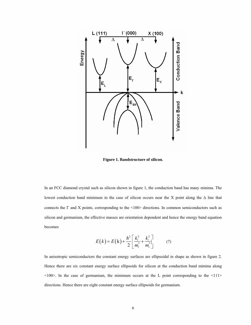
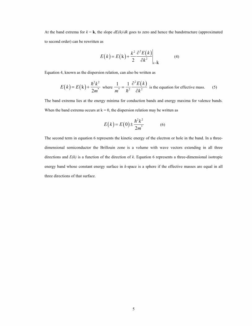
Figure 1. Bandstructure of silicon.
In an FCC diamond crystal such as silicon shown in figure 1, the conduction band has many minima. The
lowest conduction band minimum in the case of silicon occurs near the X point along the ∆ line that
connects the Γ and X points, corresponding to the <100> directions. In common semiconductors such as
silicon and germanium, the effective masses are orientation dependent and hence the energy band equation
becomes
( ) ( )2 22
* *k2
l t
l t
k kE k Em m
⎡ ⎤= + +⎢ ⎥
⎣ ⎦ (7)
In anisotropic semiconductors the constant energy surfaces are ellipsoidal in shape as shown in figure 2.
Hence there are six constant energy surface ellipsoids for silicon at the conduction band minima along
<100>. In the case of germanium, the minimum occurs at the L point corresponding to the <111>
directions. Hence there are eight constant energy surface ellipsoids for germanium.
6
ky
kx
kz
Silicon
kz
ky
kx
Germanium
Figure 2. Constant energy surface ellipsoids for silicon and germanium.
The energy relations in the valence band are more complex as the light and heavy hole valence bands are
degenerate at k = 0 leading to stronger interactions and complex bands. The parabolic approximation works
well in general for low energy electrons near the conduction band minima. In the case of high fields
electrons in the conduction band are accelerated and gain high energies. Under such circumstances the
higher order terms in the Taylor series cannot be ignored and the bandstructure becomes more complex.
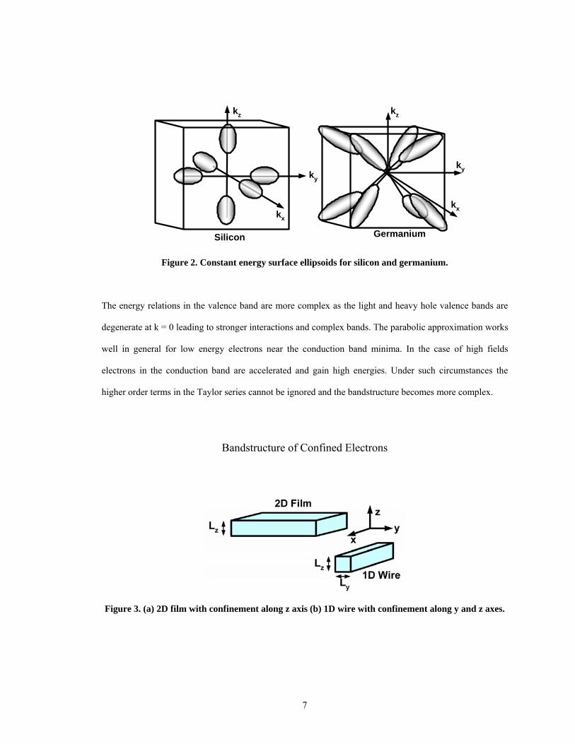
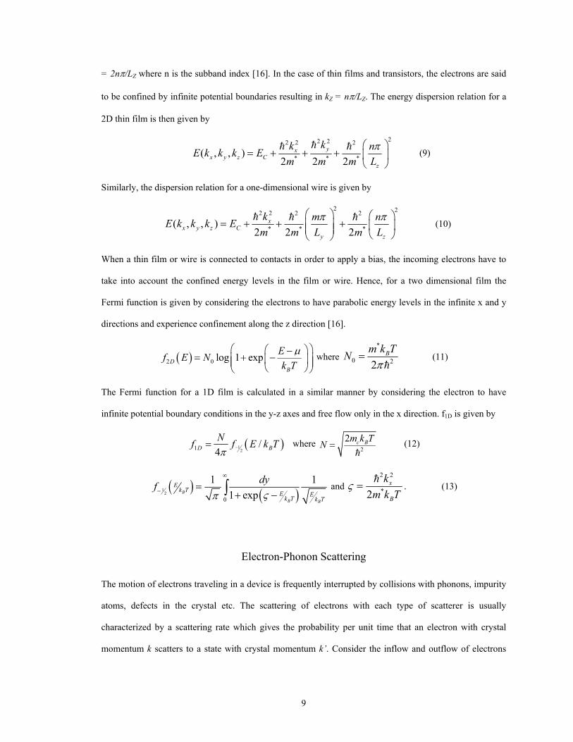
Bandstructure of Confined Electrons
Figure 3. (a) 2D film with confinement along z axis (b) 1D wire with confinement along y and z axes.
7
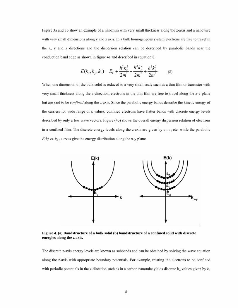
Figure 3a and 3b show an example of a nanofilm with very small thickness along the z-axis and a nanowire
with very small dimensions along y and z axis. In a bulk homogeneous system electrons are free to travel in
the x, y and z directions and the dispersion relation can be described by parabolic bands near the
conduction band edge as shown in figure 4a and described in equation 8.
2 22 2 2 2
* *( , , )2 2 2
yx zx y z C
kk kE k k k Em m m
= + + + * (8)
When one dimension of the bulk solid is reduced to a very small scale such as a thin film or transistor with
very small thickness along the z-direction, electrons in the thin film are free to travel along the x-y plane
but are said to be confined along the z-axis. Since the parabolic energy bands describe the kinetic energy of
the carriers for wide range of k values, confined electrons have flatter bands with discrete energy levels
described by only a few wave vectors. Figure (4b) shows the overall energy dispersion relation of electrons
in a confined film. The discrete energy levels along the z-axis are given by ε1, ε2 etc. while the parabolic
E(k) vs. kx-y curves give the energy distribution along the x-y plane.
Figure 4. (a) Bandstructure of a bulk solid (b) bandstructure of a confined solid with discrete energies along the z axis.
The discrete z-axis energy levels are known as subbands and can be obtained by solving the wave equation
along the z-axis with appropriate boundary potentials. For example, treating the electrons to be confined
with periodic potentials in the z-direction such as in a carbon nanotube yields discrete kZ values given by kZ
8
= 2nπ/LZ where n is the subband index [16]. In the case of thin films and transistors, the electrons are said
to be confined by infinite potential boundaries resulting in kZ = nπ/LZ. The energy dispersion relation for a
2D thin film is then given by
22 22 2 2
* * *( , , )2 2 2
yxx y z C
z
kk nE k k k Em m m L
π⎛ ⎞= + + + ⎜ ⎟
⎝ ⎠ (9)
Similarly, the dispersion relation for a one-dimensional wire is given by
2 22 2 2 2
* * *( , , )2 2 2
xx y z C
y z
k m nE k k k Em m L m L
π π⎛ ⎞ ⎛ ⎞= + + +⎜ ⎟ ⎜ ⎟⎜ ⎟ ⎝ ⎠⎝ ⎠
(10)
When a thin film or wire is connected to contacts in order to apply a bias, the incoming electrons have to
take into account the confined energy levels in the film or wire. Hence, for a two dimensional film the
Fermi function is given by considering the electrons to have parabolic energy levels in the infinite x and y
directions and experience confinement along the z direction [16].
( )2 0 log 1 expDB
Ef E Nk T
µ⎛ ⎞⎛ ⎞−= + −⎜ ⎟⎜⎜ ⎟⎝ ⎠⎝ ⎠
⎟ where *
0 22Bm k TN
π= (11)
The Fermi function for a 1D film is calculated in a similar manner by considering the electron to have
infinite potential boundary conditions in the y-z axes and free flow only in the x direction. f1D is given by
(121 /
4D BN )f f E k Tπ
−= where 2
2 c Bm k TN = (12)
( ) ( )12
0
1 11 expB
B B
Ek T E E
k T k T
dyfςπ
∞
− =+ −∫ and
2 2
*2x
B
km k T
ς = . (13)
Electron-Phonon Scattering
The motion of electrons traveling in a device is frequently interrupted by collisions with phonons, impurity
atoms, defects in the crystal etc. The scattering of electrons with each type of scatterer is usually
characterized by a scattering rate which gives the probability per unit time that an electron with crystal
momentum k scatters to a state with crystal momentum k’. Consider the inflow and outflow of electrons
9
into a specific energy level ε due to energy transitions from levels above ε2 and below this level ε1. The
energy levels are separated by an energy value of ω such that ε2 - ε = ε - ε1 = ω. In the early 20th century
Einstein proposed that if there are N photons present in a box each with energy ω, then the rate of
downward transitions is proportional to N+1 while the rate of upward transitions is proportional to N [17].
Einstein argued that this difference in the transition rates ensured that at equilibrium, the lower energy
states are more likely to be occupied than the higher energy states as predicted by the Fermi function. Since
photons and phonons are described by the Bose-Einstein distribution we can extend this argument to the
case of electron transitions due to phonon absorption and emission. The electrons and phonons are treated
as one big many-particle system whose dynamics are described by an equation similar to the Schrödinger
equation as
[ ] dH idt
ψ ψ= (14)
The vector ψ represents a state vector in a multi-particle Hilbert space that includes both electrons and
phonon systems [16]. In the many-particle system similar to a device connected to a source and drain
contacts, the N phonon subspace is coupled to the N+1 phonon subspace through phonon emission and to
the N-1 phonon subspace through phonon absorption. The emission and absorptions are peaked for phonon
energies of ω where εn - εm = ω. The transition of the electrons from εn to εm and vice versa is dependent
on the transition rate S(k, k’) which is obtained using Fermi’s Golden Rule [15]. This coupling can be
expressed through a broadening term Γ which is related to the transition rate S as
( , 'S k k )Γ= where
( ) ( ) ( ) ( )2 22 1 2em ab
nn mn n m mn n mK N K Nπ δ ε ε ω π δ ε ε ωΓ = + − − + − + (15)
The coupling constants K are expressed in the form of an interaction potential invoking the one-electron
viewpoint where a single electron feels the potential due to one phonon occupying a particular mode.
( ) ( )*em emmn m nK dr r U rφ φ= ∫ and ( ) ( )*ab ab
mn m nK dr r U rφ φ= ∫ (16)
Representing the phonon waves as plane waves with wave vector β, the interaction potential is written as
10
( ) ( ) ( ) ( ) ( ), exp . exp .ab ab em emSU r t K A r i r K A r i rβ β β ββ β= + − (17)
Substituting equation 17 into 16 and then into 15 yields the broadening matrix as
( ) ( ) ( ) ( )2 2 2 21 2em em ab ab
nm n m n mK A N K A Nβ β β βδ ε ε ω π δ ε ε ωΓ = + − − + − + (18)
Kβ is a function of the change in electronic potential energy per unit strain of the lattice. For acoustic
phonons that displace neighboring atoms in the same direction, lattice spacing is produced by the strain and
not the displacement. Optical phonons displace neighboring atoms in opposite directions and this
displacement produces a change in lattice spacing directly. Hence the scattering interaction potential for
acoustic phonons and optical phonons is written as
2 2 2AK Dβ β= and
2 2oKβ = D (19)
where DA is the acoustic deformation potential and is experimentally known for most bulk materials of
interest while Do is the optical phonons deformation potential.
|Aβ|2 is the square of the amplitude of lattice vibration. While classically the energy of vibration is
proportional to the square of its amplitude of oscillation, quantum mechanically this energy is quantized
and is given as
( )12E N ω= + where N = 0, 1, 2, ….. (20)
By equating the maximum kinetic energy of the oscillating wave to the quantum mechanical energy, the
value of |Aβ|2 is obtained as
2
2Aβ
βρ ω≈
Ω (21)
ρ is the mass density, ωβ the phonon frequency and Ω is the normalization volume. Depending on the type
of phonon that the electron interacts, the value of Kβ and Aβ can be used to calculate the broadening matrix
Γnm.
11
CHAPTER II
REVIEW OF THERMOELECTRIC MATERIALS AND MODELS
In general thermoelectric research is two-pronged with 1) experiments focused towards finding new
materials and structures with enhanced thermoelectric performance and 2) analytical models that predict
thermoelectric behavior to enable better design and optimization of materials and structures. In this paper
we present a review of the theoretical models that were developed since thermoelectricity was first
observed in 1821 by Seebeck and how these models have guided experimental materials search for
improved thermoelectric devices. A new quantum model is also presented, which provides opportunities
for optimization of nanostructured materials to enhance thermoelectric performance.
Thermoelectric Properties
When two wires of different metals are joined at both ends and the two junctions are kept at different
temperatures, a voltage develops across the two junctions. This effect is known as the Seebeck effect
which was discovered by Seebeck in 1821 and published in 1822 [18]. The voltage across the two
junctions is proportional to the temperature gradient across the junctions provided the temperature
gradient is small. The proportionality constant is defined as the Seebeck coefficient or thermoelectric
power and is obtained from the ratio of the voltage generated and the applied temperature gradient.
dVSdT
= (22)
In 1834, the Peltier effect was discovered [19]. When two metals are joined together and kept at constant
temperature while a current passes across the junction, heat is generated or absorbed at that junction in
addition to Joule heating. The Peltier coefficient Π12 is defined as the heat emitted per second when unit
current flows from conductor 1 to 2. This heat is directly proportional to the current passing through the
junction as described by equation 23.
dQ dI= ∏ (23)
12
The Thomson effect was predicted in 1854 and found experimentally in 1856 [20]. The Thomson effect
occurs when a current flows across two points of a homogeneous wire having a temperature gradient
along its length and heat is emitted or absorbed in addition to the Joule heat. The Thomson coefficient µT
is positive if heat is generated when positive current flows from a higher temperature to lower
temperature.
TTdQ dxdIx
µ ∂=
∂ (24)
These three thermal-electrical properties provide the basis for modern direct energy conversion devices and
their exploitation is the subject of considerable research.
Development of Semiconductor Thermoelectric Materials
Initial thermoelectric materials studied were metals which displayed Seebeck coefficients of a few tens of
µV/K. However, in the middle of the 20th century, interest turned towards semiconductors as thermoelectric
materials due to their high Seebeck coefficients and dominance of lattice heat conduction despite small
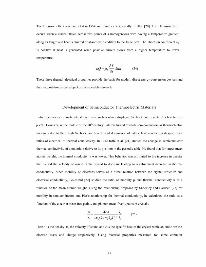
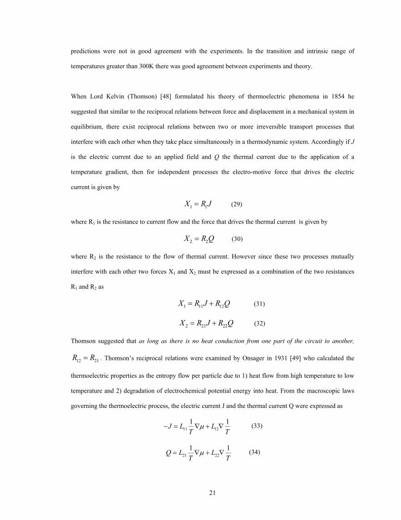
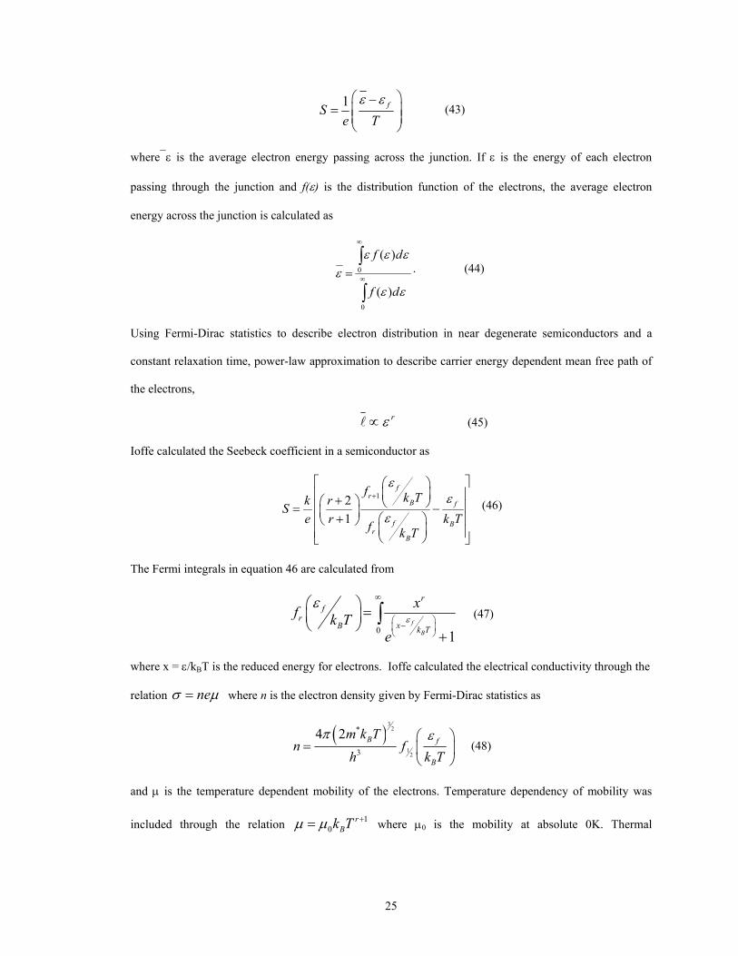
ratios of electrical to thermal conductivity. In 1952 Ioffe et al. [21] studied the change in semiconductor
thermal conductivity of a material relative to its position in the periodic table. He found that for larger mean
atomic weight, the thermal conductivity was lower. This behavior was attributed to the increase in density
that caused the velocity of sound in the crystal to decrease leading to a subsequent decrease in thermal
conductivity. Since mobility of electrons serves as a direct relation between the crystal structure and
electrical conductivity, Goldsmid [22] studied the ratio of mobility µ and thermal conductivity κ as a
function of the mean atomic weight. Using the relationship proposed by Shockley and Bardeen [23] for
mobility in semiconductors and Pierls relationship for thermal conductivity, he calculated the ratio as a
function of the electron mean free path ιe and phonon mean free ιp paths in crystals.
1
2
4(2 )
e
ps e B
lelc m k T
µ ρκ υ π
= (25)
Here ρ is the density; υs the velocity of sound and c is the specific heat of the crystal while me and e are the
electron mass and charge respectively. Using material properties measured for some common
13
semiconductors they plotted the above ratio against the mean atomic weight of the semiconductors seen in
figure 5. Applying the above mentioned selection rules of choosing materials with high Seebeck
coefficients and high atomic weights led to the discovery of Bi2Te3 in 1954 by Goldsmid and Douglas [24]
that provided cooling of 260C. Bismuth telluride has a hexagonal structure with mixed ionic-covalent
bonding along the lattice planes and the weak van der Waals bonding perpendicular to the planes. The
hexagonal structure ensures high anisotropy in the lattice conductivity with a factor of 2 decrease in the
thermal conductivity in the direction perpendicular to the planes. Bismuth telluride also has a multivalley
bandstructure with multiple anisotropic constant energy surfaces that have a small effective mass in one
direction and large effective masses in the other two directions. Since smaller effective mass lead to high
electron mobility, choosing the appropriate growth direction of bismuth telluride will ensure good
thermoelectric performance.
In 1956, Ioffe et al. [25] suggested that alloying a semiconducting thermoelectric material with an
isomorphous substance i.e. having the same crystalline structure, would enhance the figure of merit by
reducing lattice thermal conductivity without affecting carrier mobility. They suggested that phonons
would scatter due to the disturbances in the short-range order but the preservation of long-range order
would prevent scattering of electrons and holes. This led to an extensive study of the thermoelectric
performance of various semiconductor alloy systems over a wide range of temperatures.
14
1.E+03
1.E+04
1.E+05
1.E+06
0 40 80 120Mean Atomic Weight
Ele
ctro
n M
obili
ty/T
herm
al
Con
duct
ivity
( µ/ λ
)Diamond
Si
Cu2SZnO AgCl
Ge
Te
PbS
InSb
Figure 5. Ratio of electron mobility to thermal conductivity of thermoelectric materials. Reproduced from data in [22].
Birkholz in 1958 [26] and Rosi et al. in 1959 [27] showed that alloying Bi2Te3 with Sb2Te3 or Bi2Se3
greatly reduced the thermal conductivity. They also showed that adding even 5% of Sb2Se3 greatly
improved the figure of merit by raising the bandgap that reduced ambipolar conduction i.e. contribution due
to both electrons and holes to electrical conductivity and thermal conductivity. These studies led to the
formation of a pseudo-ternary Bi2Te3 - Sb2Te3 - Sb2Se3 system. The studies showed that the best n-type
material was the Bi2Te3 rich alloys while the best p-type performance was obtained from the Sb2Te3
pseudo-ternary alloys with an average figure of merit of 3.3x10⁻³K-1 from both types at room temperature
[28]. In general however, bismuth and bismuth telluride alloys are good thermoelectric materials only
below room temperature. At room temperature and above, the relatively small bandgap causes mixed
conduction due to both electrons and holes leading to reduced Seebeck coefficient.
At temperatures above those that bismuth telluride can be used, materials like lead telluride are found to
have very good thermoelectric properties in the range of 300K to 700K. Lead telluride belongs to the lead
chalcogenides system similar to materials such as PbS and PbSe. Lead chalcogenides have a cubic (NaCl)
rock-salt structure with a FCC unit cell. They are polar semiconductors with a mixed ionic-covalent bond
with the electrons traveling mainly in the cation (Pb) sublattice and the holes in the anion chalcogenide
sublattice. Similar to bismuth telluride PbTe has high mean atomic weight and a multivalley bandstructure.
Having slightly higher bandgap of 0.32eV at 300K it produces higher Seebeck coefficients. While it has
15
higher lattice thermal conductivity than bismuth telluride at room temperature, it eventually produces
higher ZT values as the temperature is raised. Lead telluride also forms isomorphous solid solutions with
lead selenide and tin telluride leading to lower thermal conductivities and improved ZT values. Rosi et al.
[28] in 1961 studied the bandgap of the PbTe-SnTe system and determined that band reversal effect
actually causes the bandgap to go to zero at the composition Pb0.4Sn0.6Te and hence recommended that
lower compositions of tin telluride would ensure sufficient bandgaps leading to ZT values near 1 for n-type
PbTe-SnTe alloys at 700K [29]. Another type of alloy system that gives ZT values around 1 for
temperature range around 700K are alloys between AgSbTe2 and GeTe called TAGS [30]. These alloys
posses the same rock-salt structure of PbTe over part of the compositional range. When the composition of
GeTe is greater than 70% it leads to a transition to rhombohedral structure. The lattice strain associated
with this phase transition is also believed to contribute to reduced lattice thermal conductivity values
around 1.5W/m-K. At higher temperature ranges of 600K to 1300K, silicon and germanium which are bad
thermoelectrics due to their high thermal conductivity at room temperature can be alloyed to obtain SiGe
alloy, a far superior material for thermoelectric generation [31]. The large bandgap of silicon makes silicon
rich alloys such as Si0.7Ge0.3 suitable for high temperature applications since problems with minority carrier
dominance do not arise. The large phonon scattering ensures low thermal conductivity without affecting the
electron mobility making it possible to obtain ZT values of 0.5 and higher [32].
Materials in general exhibit the best possible thermal conductivity in the crystalline state and the lowest
conductivity in the amorphous state. Based on this concept Slack in 1979 [33] proposed that the smallest
possible lattice conductivity can be predicted by setting the mean free path of the phonons equal to that in
the amorphous state. This observation prompted extensive research leading into materials that are termed as
phonon glass and electron crystal (PGEC). These materials have very complex structures such as
compounds of Borides (YB68) [34] and compounds of silver-thallium (TlAsSe3) [35]. These materials
contain groups of atoms or molecules that do not have precisely defined positions or orientations. The lack
of long-range order causes the atoms or molecules to rattle and act as phonon scattering sites reducing the
thermal conductivity to around 0.5W/m-K
16
Another class of materials is called Skutterudites, which are complex materials with a chemical formula of
ReTm4M12 where Re is a rare earth element such as lanthanum or cerium, Tm is a transition metal such as
cobalt, iron etc and M is metalloid such as phosphor, arsenic, or antimony. Binary skutterudites have the
chemical formula of TmM3, and its crystal structure has the unique feature of containing two large empty
spaces within each unit cell. While the binary structures have reasonably large Seebeck coefficients of
around 200µV/K, they still exhibit very high thermal conductivities [29]. When a rare earth element is
mixed with the binary skutterudite, the heavy atom of the rare earth element occupies the empty space of
the crystal [36]. In addition to causing large impurity scattering of phonons in these materials, the loosely
bound heavy atoms rattle in their cages enhancing scattering of phonons and reducing thermal conductivity
by an order of magnitude at room temperature. Skutterudites have been found to have a figure of merit
greater than one at temperatures around 700K.
Additional examples of PGEC materials are inorganic clathrates with the chemical formula A8B46 where B
represents for example either gallium or germanium or a combination of the two elements [29]. These
materials are found to be very promising for power generation at temperatures above 600ºC. Clathrates
consist of an open framework of gallium and germanium atoms that act as an electron crystal. Guest atoms
are selectively incorporated in nanocavities in the crystal. The guest atoms vibrate independent of the
crystal structure scattering phonons in the process. Clathrates can be made of tin, silicon, antimony etc.
Examples of some good thermoelectric clathrates are Sr8Ga16Ge30, Cs8Sn44 as well as well as Zn4Sb3 that
has been observed to give ZT values of 1.3 at 400K. More recently an alloy of Pb-Sb-Ag-Te abbreviated as
LAST was developed as n-type thermoelectric material having ZT values around 1.7 [37, 38]. These alloys
have nano-sized inclusions during synthesis that act as phonon scattering sites. A similar p-type alloy
dubbed as SALT was observed to have ZT values around 1.6, the highest known for p-type thermoelectric
materials.
In addition to the development of bulk materials with enhanced thermoelectric properties, the development
of superlattices to improve ZT has led to research in superlattices made from alloys that are good
thermoelectric materials to start with such as Bi2Te3/Sb2Te3, Bi2Te3/Bi2Se3 as well as PbSeTe/PbTe
17
quantum dot superlattices, Si/Si1-xGex and Si/Ge superlattices [8]. While fabrication of superlattice films
and wires can take advantage of the advances made in semiconductor manufacturing technology such as
molecular beam epitaxy, metallorganic chemical vapor deposition etc, significant challenges exist in
translating the high ZT performance of bulk materials into similar performance in nanoscale applications.
In this regard the biggest bottleneck is the electrical conductivity which is dominated by contact resistance.
The anisotropic nature of most nanoscale materials also makes their thermal conductivity performance
unpredictable and hard to measure. Measurement of thermoelectric properties at the nanoscale is especially
hard as the substrate and buffer layers can overwhelm the Seebeck coefficient and electrical conductivity
measurements. The challenges and high costs associated with nanoscale measurements places special
emphasis on the need to have a detailed understanding of electron-hole-phonon transport at the nanoscale
so as to better predict thermoelectric performance. Quantum confinement effects while increasing the
density of states per unit volume at the Fermi level can also lead to reduced electrical conductivity due to
the limited energy states available for electron transport. Similarly while phonon scattering and
confinement at the superlattice interfaces can lead to reduced thermal conductivity, its impact on electron
and hole transport through confined carrier-phonon scattering also has to be better understood. There has
never been a greater need for a strong model that can couple both quantum and scattering effects to predict
transport behavior in nanoscale devices.
Development of Modeling of Thermoelectric Coefficients
In 1928, A. Sommerfeld [39] put forth a comprehensive model on free electron theory in metals using
Fermi-Dirac statistics instead of Maxwellian statistics for the free electron theory in metals developed by
Lorentz. Sommerfeld assumed that only the valence electrons in a metal formed a free electron gas that
obeyed the Fermi-Dirac distribution. In 1931, Sommerfeld and Frank [40] studied thermoelectric
phenomena in metals studied where various combinations of the electric current and temperature gradient
∂T/∂x were applied on a wire. From their calculations they obtained equations for the electrical
conductivity σ, thermal conductivity κ and Thomson coefficient µT. In all the calculations Sommerfeld and
18
Frank assumed conditions of local equilibrium and the number of electrons to be independent of
temperature and the mean free path of the electrons to be independent of their velocity.
( )32
20
0
43
e m f v dvm h v
πσ∞ ∂⎛ ⎞= ⎜ ⎟ ∂⎝ ⎠ ∫ (26)
( )
( )
43 0
5 30 0 0
20 00
0
46
f v dvvf fm m v
h x xf v dv
v
πκ
∞
∞ ∞
∞
⎡ ⎤∂⎢ ⎥∂∂ ∂⎛ ⎞ ⎢ ⎥= −⎜ ⎟ ⎢ ⎥∂ ∂∂⎝ ⎠⎢ ⎥
∂⎣ ⎦
∫∫ ∫
∫v dv (27)
2 2
2
23
Bmk Teh
2π λµ = (28)
where λ is the de Broglie wavelength of electrons.
Bloch [41] solved the wave equation for periodic metallic lattice and showed that if the lattice is perfect,
the electron would travel infinitely through it and only by taking into consideration the thermal motion of
the lattice and the effect of impurities would finite conductivity be obtained. In addition, Bloch showed that
the application of Pauli’s exclusion principle eliminated the direct proportionality between the number of
free electrons and the electrical conductivity. Conduction under an applied field would then take place only
if the final energy levels are unoccupied such that the electrons near the Fermi level can make transitions
and take part in conduction. Bloch called these electrons conduction electrons. Based on these ideas Bloch
introduced temperature dependence of electronic conduction in metals where the electric resistance varied
directly with the absolute temperature for high temperatures and varies as T5 for low temperatures. Bloch’s
theory of electrical conduction could not be easily extended to semiconductors as it seemed to suggest that
a lattice should have nearly infinite conductance at low temperatures while in reality the conductivity of
semiconductors is very low at low temperatures due to limited number of free electrons. It also could not
explain the non-conductivity of insulators. In 1931, A. H. Wilson [42] extended Bloch’s theory to
semiconductors and developed a formal theory of electron transport in semiconductors and insulators with
emphasis on the temperature dependence of electrical conductivity. Wilson’s work was further extended to
study Hall coefficients and thermoelectric power of semiconductors by M. Bronstein [43] in 1932 and R. H.
19
Fowler [44] in 1933 but neither of the results by these authors were in a form suitable for comparison with
direct experimental data or predictions of thermoelectric power from measured Hall and resistivity data.
In his book The Theory of Metals in 1953 Wilson [45] gave a comprehensive analysis of the conduction
mechanism and thermoelectric performance of metals and semiconductors under the relaxation time
approximation taking into account the effect of electron scattering with acoustic and optical phonons and
electron-impurity scattering. Based on his calculations, the relaxation time in metals for electron-phonon
scattering was calculated to be proportional to E3/2T-1 which is the same result shown by Bloch for metals.
In the case of semiconductors the distribution of electrons is taken to be ( )ε-εfk TB
-0f =exp and restricting the
phonon energy range to values around the Fermi energy εf, Wilson calculated the electrical conductivity to
be proportional to nm*-5/2T-3/2. By arriving at a direct proportionality between the conductivity and number
of free electrons n, Wilson was able to show that semiconductors have very low conductivity at low
temperatures due to the very small number of free electrons available for conduction.
In 1953 Johnson and Horovitz [46] used Sommerfeld’s model of electric current and thermal current to
calculate thermoelectric coefficients for three different cases. 1) Impurity temperature range where all the
carriers are either n-type or p-type such that the concentration of carriers remains constant with temperature
until intrinsic carrier effects become important. 2) Transition temperature range where in addition to n and
p type carriers, intrinsic carriers also exist and hence ne ≠ nh. 3) Intrinsic temperature range where intrinsic
carrier dominate the electrons and holes from donors and acceptors such that ne = nh. The authors used
Maxwell statistics to describe the carrier distribution in the semiconductors. The mean free path was said to
be affected by lattice vibrations where similar to Sommerfeld, it was expressed to be independent of carrier
energy. In the impurity and transition range an additional mean free path due to impurities was included
where the mean free path was expressed as a function of carrier energy as limp = aε2. The thermoelectric
power for polycrystalline germanium having carrier concentrations ranging from 1015cm3 to 7x1018cm3 was
calculated using these equations and compared to experiments conducted by Lark-Horovitz, Middleton,
Miller Scanlon and Walerstein [47] over a temperature range of 78K to 925K. For impurity temperature
range of approximately 78K to 300K there was lot of scatter in the experimental data and the theoretical
20
predictions were not in good agreement with the experiments. In the transition and intrinsic range of
temperatures greater than 300K there was good agreement between experiments and theory.
When Lord Kelvin (Thomson) [48] formulated his theory of thermoelectric phenomena in 1854 he
suggested that similar to the reciprocal relations between force and displacement in a mechanical system in
equilibrium, there exist reciprocal relations between two or more irreversible transport processes that
interfere with each other when they take place simultaneously in a thermodynamic system. Accordingly if J
is the electric current due to an applied field and Q the thermal current due to the application of a
temperature gradient, then for independent processes the electro-motive force that drives the electric
current is given by
1 1X R J= (29)
where R1 is the resistance to current flow and the force that drives the thermal current is given by
2 2X R Q= (30)
where R2 is the resistance to the flow of thermal current. However since these two processes mutually
interfere with each other two forces X1 and X2 must be expressed as a combination of the two resistances
R1 and R2 as
1 11 12X R J R Q= + (31)
2 21 22X R J R Q= + (32)
Thomson suggested that as long as there is no heat conduction from one part of the circuit to another,
. Thomson’s reciprocal relations were examined by Onsager in 1931 [49] who calculated the
thermoelectric properties as the entropy flow per particle due to 1) heat flow from high temperature to low
temperature and 2) degradation of electrochemical potential energy into heat. From the macroscopic laws
governing the thermoelectric process, the electric current J and the thermal current Q were expressed as
12 21R R=
11 121J L LT T
µ 1− = ∇ + ∇ (33)
21 221 1Q L LT T
µ= ∇ + ∇ (34)
21
L11, L12 and L22 are called kinetic coefficients and are properties of the medium such as electrical
conductivity, thermal conductivity etc and in the absence of a magnetic field, Onsager stated that
12 21L L= (35)
Callen in 1948 [50] showed that while Onsager’s relations strictly referred to specific transient irreversible
processes, they could be extended to steady state processes by considering the system to be the limiting
case of many small sections, each in local equilibrium. This assumption is incorporated by treating the
temperature T and Fermi energy εf as functions of position. Callen pointed out that this assumption was
similar to the assumptions made while using the Boltzmann transport equation where the system is assumed
to be in local equilibrium by incorporating the deviation from equilibrium term in the calculations.
In 1953 Frederikse [51] noticed large anomalies in the predicted vs. measured thermoelectric power in
germanium below temperatures of 200K. They attributed these anomalies to the assumption of lattice
thermal equilibrium commonly made when calculating thermoelectric coefficients. The deviation from
equilibrium of the lattice at low temperatures results in a phonon current that interacts with the electron
current. Frederikse modified Horovitz’s model to include an additional term inversely proportional to
temperature that would account for the deviation from equilibrium of the lattice at lower temperatures.
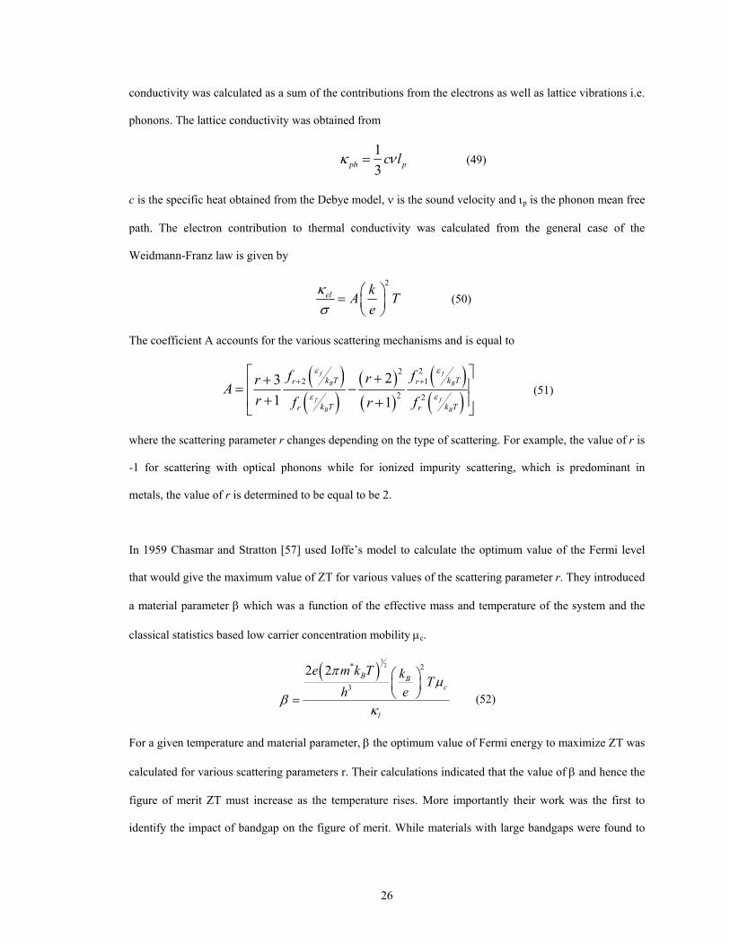
Onsager’s reciprocal relations were used by P. J. Price [52] in 1956 where he used a modification of the
Johnson-Horovitz model [53] to calculate the thermoelectric coefficients in isotropic semiconductors. The
thermoelectric parameters were calculated phenomenologically as a function of the electron and hole
conductivities using average values of the electric and thermal current.
.J Jσ = (36a)
1 .S JTσ
= Q (36b)
1 .e Q QT
κ = (36c)
The carrier energy was said to be affected by contributions from 1) electrostatic field 2) band edge energies
3) bandgap and at low temperatures 4) entrainment of the lattice energy due to carrier-lattice collisions
22
known as phonon-drag effect. The resulting expression for thermoelectric power was expressed in terms of
the electron and hole electrical conductivities as
( ) ln2
eBe h
h
kSe
σα σ σ σ σξσ σ
⎡ ⎤⎛ ⎞= − − −⎢ ⎥⎜ ⎟
⎢ ⎥⎝ ⎠⎣ ⎦ where e hσ σ σ= + and
32
log e e
h h
mm
µξµ
⎛ ⎞⎛ ⎞⎜ ⎟= ⎜ ⎟⎜ ⎟⎝ ⎠⎝ ⎠
(37)
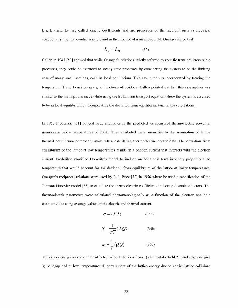
Price assumed that the electron and hole mobilities were independent of doping and used the S vs. σ plot to
graphically obtain the value of α, a function of the material bandgap, as shown in equation 38. Price
showed that the graph, seen in figure 6, formed a loop where n-type materials are at the bottom of the loop
and p-type materials at the top. The value where σe = σh corresponded to the minimum value of σ where
minimum thermoelectric power is obtained due to bipolar transport. In addition to the thermoelectric loop,
another notable contribution made by Price was the study of the change in thermoelectric power of
semiconductors under shear strain. He showed that shear strain would change the activation energy of the
impurity donor atom binding a carrier in a many-valley band by decoupling the orbitals associated with the
different valleys leading to a shift in the band edge energies. Price recognized that this shift in the band
edge energies of the donor atoms would appreciably change the thermoelectric power of semiconductors
especially at very low temperatures.
S
Sx= 0
logσ0 logσx logσ
Xp-type
n-type
Figure 6. Price’s doping curve for thermoelectric power. Reproduced from [52]
23
0
22 log 1Xσα ασ
⎛ ⎞= ⎜ ⎟
⎝ ⎠… . (38)
In 1912, Altenkirch [54, 55] introduced the concept of a figure of merit when he showed that good
thermoelectric materials should possess large Seebeck coefficients, high electrical conductivity to minimize
Joule heating and low thermal conductivity to retain heat at the junctions that will help maintain a large
temperature gradient. Ioffe in 1957 [56] presented the figure-of-merit in its present form Z= S2σ/κ which he
used to qualify the efficiency of thermoelectric materials. Ioffe gave a simple explanation to calculate the
Seebeck coefficient based on thermodynamic considerations. Consider a junction of two conductors
through which one coulomb of charge passes at an infinitesimally slow rate such that the current is very
small. The entire circuit is assumed to be at constant temperature T such that there is no heat conduction or
joule heat loss allowing the system to be treated to be in equilibrium. Since the two conductors are in
equilibrium their chemical potentials are equal such that1 2f f fε ε ε= = . For a reversible, open system,
the conservation of energy equation can be written as
fU Ts ε= + (39)
The average energy U as well as the entropy s of the electrons in the two conductors is different. Since the
chemical potential of the two conductors us equal, we can write
1 1 2U Ts U Ts2− = − (40)
When an electron passes through a junction of two conductors its average energy changes by U1-U2. This
difference in electron energy is generated in the form of Peltier heat Π1-2 at the junction.
1 2 1U U 2−− = ∏ (41)
The relation between Peltier heat and Seebeck coefficient is given by ST = Π1-2. From equations 40 and 41
the Seebeck coefficient is obtained as
1 2 1 21
U US ST T
−2S∏ −
= = = − (42)
Equation 42 describes the Seebeck coefficient as the flow of entropy per unit charge across a junction.
From this definition and equation 39, the Seebeck coefficient across the junction can be written as
24
1 fSe T
ε ε⎛ ⎞−= ⎜⎜
⎝ ⎠⎟⎟
(43)
where⎯ε is the average electron energy passing across the junction. If ε is the energy of each electron
passing through the junction and f(ε) is the distribution function of the electrons, the average electron
energy across the junction is calculated as
0
0
( )
( )
f d
f d
ε ε εε
ε ε
∞
∞=∫
∫. (44)
Using Fermi-Dirac statistics to describe electron distribution in near degenerate semiconductors and a
constant relaxation time, power-law approximation to describe carrier energy dependent mean free path of
the electrons,
rε∝ (45)
Ioffe calculated the Seebeck coefficient in a semiconductor as
121
fr
B f
f Br
B
f k Tk rSe r k Tf k T
εε
ε
+
⎡ ⎤⎛ ⎞⎜ ⎟⎢ ⎥+⎛ ⎞ ⎝ ⎠⎢ ⎥= −⎜ ⎟+ ⎛ ⎞⎢ ⎥⎝ ⎠
⎜ ⎟⎢ ⎥⎝ ⎠⎣ ⎦
(46)
The Fermi integrals in equation 46 are calculated from
0 1f
B
rf
rxB k T
xf k Te
ε
ε ∞
⎛ ⎞−⎜ ⎟⎝ ⎠
⎛ ⎞ =⎜ ⎟⎝ ⎠
+∫ (47)
where x = ε/kBT is the reduced energy for electrons. Ioffe calculated the electrical conductivity through the
relation neσ µ= where n is the electron density given by Fermi-Dirac statistics as
( )3
2
12
*
3
4 2 B f
B
m k Tn f
h k
π ε⎛ ⎞= ⎜
⎝ ⎠T ⎟ (48)
and µ is the temperature dependent mobility of the electrons. Temperature dependency of mobility was
included through the relation 10
rBk Tµ µ += where µ0 is the mobility at absolute 0K. Thermal
25
conductivity was calculated as a sum of the contributions from the electrons as well as lattice vibrations i.e.
phonons. The lattice conductivity was obtained from
13ph pc lκ ν= (49)
c is the specific heat obtained from the Debye model, ν is the sound velocity and ιp is the phonon mean free
path. The electron contribution to thermal conductivity was calculated from the general case of the
Weidmann-Franz law is given by
2
el kA Te
κσ
⎛ ⎞= ⎜ ⎟⎝ ⎠
(50)
The coefficient A accounts for the various scattering mechanisms and is equal to
( )( )
( )( )
( )( )
222 1
2 2
231 1
f f
B B
f f
B B
k T k Tr r
k T k Tr r
f frrAr f fr
ε ε
ε
+ +⎡ ⎤++⎢ ⎥= −
+⎢ ⎥+⎣ ⎦ε
(51)
where the scattering parameter r changes depending on the type of scattering. For example, the value of r is
-1 for scattering with optical phonons while for ionized impurity scattering, which is predominant in
metals, the value of r is determined to be equal to be 2.
In 1959 Chasmar and Stratton [57] used Ioffe’s model to calculate the optimum value of the Fermi level
that would give the maximum value of ZT for various values of the scattering parameter r. They introduced
a material parameter β which was a function of the effective mass and temperature of the system and the
classical statistics based low carrier concentration mobility µc.
( )3
2* 2
3
2 2 B Bc
l
e m k T k Th e
πµ
βκ
⎛ ⎞⎜ ⎟⎝ ⎠= (52)
For a given temperature and material parameter, β the optimum value of Fermi energy to maximize ZT was
calculated for various scattering parameters r. Their calculations indicated that the value of β and hence the
figure of merit ZT must increase as the temperature rises. More importantly their work was the first to
identify the impact of bandgap on the figure of merit. While materials with large bandgaps were found to
26
have low carrier mobility and high thermal conductivity, small bandgap materials would result in low ZT
values at high temperatures due to increased minority carrier contribution to thermal conductivity. In
addition ionic compounds were considered to be bad thermoelectric materials due to very high polar
scattering of electrons decreasing the mobility. Chasmar and Stratton combined their analysis with the
results of Goldsmid [22] whose studies on the ratio of mobility to thermal conductivity as a function of the
atomic weight led to the discovery of bismuth telluride. From their analysis semiconductors with best
values of β between 0.1 and 0.2 and high atomic weight comprised of sulphides, selenides and tellurides of
heavy metals such as lead or bismuth. Though these compounds have low bandgap at 0K (≤ 0.22eV), the
bandgap increases as the temperature increases. Cadmium telluride on the other hand has a large bandgap,
1.45eV at 300K but the material parameter β is only 0.03-0.06. Based on the above studies Chasmar and
Stratton proposed that a combination of cadmium telluride or selenide (large bandgap, small β) with a
telluride or selenide of small bandgap and large β would result in a good thermoelectric material.
Attempts to find an upper bound to the figure of merit were made by various researchers. Littman and
Davidson [58] used irreversible thermodynamics to show that no upper limit was imposed on ZT by the
second law. However, Rittner and Neumark [59] showed that it was important to employ a combination of
statistical or kinetic methods with a proper physical model of semiconductors to study the figure of merit.
Simon [60] studied the optimum ZT value in two band semiconductors as a function the minimum bandgap
ηg, material parameter β for electrons and holes and the scattering parameter r for electrons and holes. He
defined a parameter γ = (me/mh)3/4(µce/µch)1/2 that he varied by varying the material parameters βe and βh.
While he could not arrive at a definite upper limit to the value of ZT his theoretical studies of optimum ZT
vs. γ for ηg = 0 showed that very high values of ZT could be achieved in very small bandgap
semiconductors by doping.
Significant progress was made in the fifties and the sixties towards analytically calculating the scattering
parameters used in the Boltzmann transport equation. The most common modes of scattering included in
the BTE were acoustic phonon scattering through the deformation potential put forth by Bardeen and
Shockley [6] and the polar-optical mode scattering put forth by Callen in 1949 [61] and Frohlich in 1954
27
[62]. In the case of elastic scattering such as acoustic phonon scattering and ionized-impurity scattering,
the relaxation time approach that characterizes the rate at which momentum decays can be used to solve the
BTE. However in the case of inelastic scattering no relaxation time exists and hence other methods to solve
the BTE were developed such as the variational calculations approach put forth by Kohler in 1948 [63], the
iteration method by Rode in 1970 [64] and the matrix method by Kranzer in 1971 [65]. Meanwhile Kane in
1957 [66] determined accurately the structure of the lowest (000) conduction band minima at the center of
the Brillouin zone as well as the wave functions in that valley. Using Kane’s model of the band structure
and electron wave functions, Rode calculated the electron mobility in intrinsic, direct gap, polar, non-
degenerate semiconductors using Maxwellian statistics. He included the three scattering mechanisms i.e.
acoustic deformation potential scattering, polar optical phonon scattering and piezoelectric scattering which
he identified as the most important mode of scattering for lower lattice temperatures such as for e.g. below
60K in GaAs. The electron distribution function under the influence of a small electric field is described as
a linear finite-difference equation, which was solved using a numerical iteration method. The mobilities
resulting from using parabolic vs. non-parabolic bands described by Kane were compared. Non-
parabolicity affected the calculated mobility by only 10% in wide bandgap material such as GaAs while
small bandgap material such as InSb showed a 50% decrease in the calculated mobility when non-
parabolicity was included. Good match between the predicted and measured mobility data was seen for
GaAs between the temperature ranges of 150K to 400K. While the poor match with measured data at high
temperatures could not be explained, the results below 150K were attributed to the non-inclusion of
impurity scattering in the model which becomes prominent at low temperatures. In 1971 Rode [67]
extended the previous study to calculate mobility and thermoelectric power in degenerate direct-gap, polar
semiconductors using Fermi-Dirac statistics. In addition to piezoelectric scattering, longitudinal acoustic
phonon scattering and polar-optical phonon scattering, ionized-impurity scattering and heavy hole
scattering were also included in the calculations. Thermoelectric power was calculated from the short-
current calculated from the perturbation distribution where the field is set equal to zero.
1f
JeQ
T
εσ
⎛ ⎞∇ +⎜ ⎟⎝ ⎠= −
∇ (53)
28
Mobility and thermoelectric power were compared with experimental data for intrinsic InSb, InAs and InP.
There was good agreement with measured mobility data for all three semiconductors above room
temperature while below room temperature the mobility showed two orders of magnitude decrease
compared to experiments. Electron-hole scattering was prominent above room temperature, polar mode
inelastic scattering dominated at room temperature while impurity scattering was dominant below room
temperature. Below 60K in InSb and 80K in InAs, deformation potential acoustic mode scattering and
piezoelectric scattering dominate electron mobility. Good agreement with experimental data was also seen
in the case of thermoelectric power for various electron concentration levels at room temperature.
However, for higher temperatures, the thermoelectric power showed slight deviation from experiments
where multi-valley conduction was suspected to dominate electron transport.
Sofo and Mahan in 1994 [68] extended Rode’s work to study the optimum bandgap in direct bandgap
semiconductors. Non-parabolicity was included using the two-band Kane model and the solution to the
BTE was obtained using Rode’s iteration method in the Gauss-Siedel formulation because inelastic
scattering was included. Comparisons were made between ZT values for parabolic bands and non-parabolic
bands with either elastic ionized impurity scattering or inelastic polar optical phonon scattering. They found
that the dependence of ZT on the bandgap Eg fell into two regimes. For Eg < 6kBT the value of ZT
decreased with decreasing bandgap due to the increasing presence of minority carriers. For Eg > 10kBT the
value of ZT either increased or decreased depending upon the type of scattering involved. Additionally they
found that the most important effect of non-parabolicity was to modify the effective mass values that in
turn changed the value of the material parameter B0 present in the expression for ZT similar to the
parameter B in Chasmar and Stratton’s model. Mahan determined that in order to obtain higher ZT values
the value of B0 need to increase implying that materials with higher effective masses or reduced thermal
conductivity κ needed to be researched.
29
Development of Low-Dimensional Models for Thermoelectric Applications
The concept of monocrystalline semiconductor structures having a periodic potential in one-dimension was
proposed by Esaki and Tsu in 1970 [69] who called these structures superlattices. They suggested that the
periodic potential could be obtained by periodic variation of alloy composition or variation of impurity
density during epitaxial growth out of materials such as Si, Ge and their alloys, III-V, II-VI, compounds
and their alloys etc. The dispersion relation in the direction parallel to the superlattice planes was assumed
to be parabolic while in the cross-plane direction they used a sinusoidal approximation in the form of
Mathieu’s equation [70].
( ) ( )( )2 2
*, 1 cos2
kE k k t k d
m⊥ ⊥= + − (54)
where d is the superlattice period and t is the amplitude of the superlattice periodic potential. The authors
found that under moderate electric fields in the cross-plane direction the confined energy bands and wave
vector zones would result in a negative conductance that could lead to new ultra-high frequency oscillators.
The negative conductivity will arise from the fact that electrons traveling perpendicular to the superlattice
would experience negative effective mass beyond the inflection point in the sinusoidal dispersion relation.
In 1984 Friedman [71] proposed that the low temperature (kBT <µ) thermoelectric power S of a superlattice
as a function of dopant concentration can be used to provide information about the one-electron density of
states and the location and width of the mini-bands. Following Wilson’s model for calculating
thermoelectric power using Fermi-Dirac statistics in the BTE and assuming energy-independent momentum
scattering rates, they showed mathematically that the thermoelectric power tends to diverge at the mini-
band extrema. The divergence in S is smoothed out for energies greater than kBT but they were still
discernible for low temperatures. In addition, anisotropy in the thermoelectric power was predicted for in-
plane vs. cross-plane temperature gradient. For the next couple of years the low-temperature thermoelectric
power of superlattices was predominantly used as a tool to understand the electronic structure and transport
properties of superlattices [72, 73] as well as the scattering dynamics of electrons and phonons in solids
[74, 75].
30
In 1992, Mensah and Kangah [76] used the relaxation time approximation (RTA) model of the BTE with
the sinusoidal dispersion relation for the confined direction of superlattices to obtain analytical expressions
for the Seebeck coefficient and thermal conductivity of superlattices along the superlattice cross-plane
direction. Defining 2∆ as the width of the lowest energy mini-band in the E vs. k regime, the thermopower
and thermal conductivity are calculated for two ranges of ∆. For ∆ << kBT, the electrons in the superlattice
are said to behave as a 2D electron gas while for ∆ >> kBT the electrons behave as a 3D gas. They
suggested that by an optimal selection of ∆ and d, the superlattice period it is possible to obtain good-
quality and efficient thermoelements. In 1993, Dresselhaus and Hicks [77] proposed that by layering highly
anisotropic thermoelectric materials such as Bi2Te3 alloys in the form of superlattices would make it
possible to increase the figure of merit provided that the superlattice multilayers are made in a particular
orientation. The model of the superlattice proposed by the authors involved layers of thin films with no
barrier layers such that confinement effects originated only due to electron confinement in the thin films.
They theorized that in addition to confinement effects that cause electrons to behave as a 2D gas, the
layering would reduce thermal conductivity through phonon scattering and thus increase ZT. The layers
were assumed to be parallel to the x-y plane where they have a parabolic dispersion and a confined
dispersion in the z direction as shown in equation 55 which unlike the sinusoidal dispersion used in the
previous papers, treats the lowest subband in the well to be flat similar to electrons confined in an infinite
potential well.
( )2 22 2 2 2
* * *,2 2 2
yxx y
x y z
kkk km m m a2
πε = + + where a is the layer thickness. (55)
Using the dispersion relation and the equations for S, σ and κel and κph specified by Rittner [43] they
calculated the figure of merit ZT for transport along the x-axis in terms of the reduced Fermi energy εf* and
a material parameter B described in equation 56.
2 2
* 2* 2f
zf
B
m ak T
πεε
⎛ ⎞−⎜ ⎟
⎝ ⎠= and ( )1
22
2
212
B xBx y
ph
k Tk TB m ma e
µπ κ
⎛ ⎞= ⎜ ⎟⎝ ⎠
(56)
The authors analyzed that the value of Z2DT can be increased by using narrower layers that will ensure
increased phonon scattering and by choosing optimum current direction and layer orientation to maximize
31
mobility. The Z2DT values for Bi2Te3 were predicted for two orientations of the multilayers, the x-y planes
and the x-z planes. The results predicted an increase in ZT by a factor of 13 over the bulk value in the x-z
plane for current flow along the x-axis for layers that are 3.8D thick. In the case of the x-y plane results
predicted an increase in ZT by a factor of 3 over the bulk value for layers that are 10D thick. The dispersion
model used in the above paper treats the quantum wells as decoupled such that there is no tunneling
between the wells.
Sofo and Mahan [78] analyzed the ZT predictions of a superlattice put forth by Hicks and Dresselhaus by
incorporating alternating barrier layers having finite thermal conductivity in the superlattice and introduced
a tunneling probability between the quantum wells in their calculations. They argued that quantum mixing
between the wells due to tunneling leads to a broadening of the density of states from 2D to 3D. In
addition, the finite thermal conductivity of the barrier region produces a parasitic effect of backflow of heat
that would hinder the pumping of heat in the well. The authors used the RTA model to include electron
density dependence on the electrical conductivity through the expression given by Wilson [45].
2
x
en mτσ ⎛= ⎜
⎝ ⎠⎞⎟ (57)
The dependence of the electrical conductivity on electron density ensures that if the well width a and
chemical potential εf are kept constant, just by increasing the barrier width b, the electron density will
decrease due to reduced tunneling probability causing the electrical conductivity to decrease and decrease
ZT. Alternately, for a fixed barrier width, as the well width is reduced, the two-dimensional density of
states increases and proportionately increases the electrical conductivity as well as ZT. The thermal
conductivity equation was also modified to include heat backflow at the barriers in the thermal
conductivity. In addition they changed the value of B to be inversely proportional to the superlattice period
d and not the well thickness a. Sofo and Mahan used their model to predict the ZT vs. well width values for
Bi2Te3 layers in the x-y plane with transport along the x-axis. Using average values in the literature for the
mobility µx and thermal conductivity κ, they found that there was improvement in ZT due to the
enhancement of density of states at the bottom of the lowest subband with decreasing well width but the
amount of increase was not as high as originally predicted by Dresselhaus and Hicks. The change in ZT
32
with decreasing well width was studied as a function of the barrier width. In all cases except for a 20D wide
barrier the ZT values increase with decreasing well thickness. The decrease in ZT for the 20D barrier was
attributed to tunneling through the barrier that causes quantum coupling between the wells leading to
broadening of density of states making the 2D density of states to become 3D density of states and reduce
ZT. The authors also point out that the flat subband assumption works well when the Fermi level lies above
the subband at a distance greater than the value of kBT as electrons above and below the Fermi level have
opposite contribution to the thermopower. Similar studies on the effect of tunneling and finite thermal
conductivity contribution of the barrier material were done by Broido and Reinecke [79] in 1995 who
studied the effects of confinement on the figure of merit of Bi2Te3 superlattices using Kronig-Penny type
subband energy dispersion in the RTA model. They too found that the value of ZT2D increased as the well
width decreased until tunneling between wells caused the value of ZT2D to reduce for further decrease in
well width.
In 2001 Broido and Reinecke [80] extended the BTE model with Kronig-Penny subbands to calculate
thermoelectric coefficients in quantum well and quantum wire superlattices. The thermoelectric coefficients
were calculated for the occupied subbands in each conduction band valley neglecting inter valley
scattering. The results for each valley were summed over all the multiple ellipsoidal conduction band
valleys to obtain the overall thermoelectric coefficients. Elastic acoustic phonon scattering through the
deformation potential scattering and inelastic optical phonon scattering using the solution to the inelastic
3D Boltzmann transport equation were included in the calculations. Optical phonons were assumed to be
dispersionless with the dominant phonon energy to be the value of its zone center ω0. The BTE solution
for inelastic scattering was obtained by using an extension of Ritz’s iterative method [81]. The
thermoelectric coefficients were compared to the results of the constant relaxation time approximation
(CRTA) and bulk values as a function of decreasing well width. In general, solutions based on the CRTA
were found to predict much higher values for mobility compared to the inelastic solution. Power factor
predictions made by both CRTA and inelastic scattering methods predicted lower values than the bulk
which were attributed to electron confinement in the wells leading to reduced conductivity. The power
factor values increased with decreasing well width due to increase in the 2D density of states and
33
eventually matched the bulk power factor. However, further decrease led to electron tunneling that changed
the 2D density of states to 3D lowering the power factor. These effects as seen previously were not
captured by the CRTA model. The effect of scattering and bandstructure on the thermoelectric performance
was demonstrated through the power factor studies done on two materials, PbTe and GaAs. PbTe has an
anisotropic multivalley bandstructure while GaAs has a single isotropic conduction band valley. At room
temperature both acoustic-phonon and optical-phonon scattering dominate in PbTe while only optical-
phonon scattering dominates in GaAs. Accordingly the full solution of the BTE including elastic acoustic
phonon and inelastic optical-phonon scattering showed an increase of only a factor of two in the power
factor of PbTe compared to its bulk value while GaAs showed a factor of 9.5 increase in its power factor.
The ability to incorporate the full bandstructure information to calculate the thermoelectric coefficients was
demonstrated by Sofo et al. in 2003 [82] when they presented a method of calculating the electronic
structure from first principle calculations, which they included in the relaxation time approximation to
calculate the transport coefficients. They defined a kernel of all transport coefficients known as the
transport distribution that contains all the electronic information needed to obtain the thermoelectric
coefficients directly for any given material.
k k kk
v v τΞ = ∑ . (58)
The group velocity values are obtained using the linear augmented plane wave (LAPW) method while the
relaxation times are calculated for various scattering mechanisms using parameters found in literature.
Doping was included by changing the relative position of the Fermi level under the assumption that the
bandstructure remains unchanged as the Fermi level changes. The above method was used to calculate the
thermoelectric coefficients for Bi2Te3 using experimentally determined thermal conductivity values for the
various planes. The Seebeck coefficient for all doping levels was calculated using a constant relaxation
time that gave the best fit with experimental data in the intrinsic region. For all doping levels, the Seebeck
coefficient of the n-type material showed a better fit with experiments compared to the p-type. The model
also captured effectively the anisotropy in the electrical conductivity of Bi2Te3 where the conductivity
along the basal plane can be four times greater than the conductivity along the trigonal axis. The
34
predictions for the figure of merit however did not show very good match with experiments with results for
the n-type matching better than those for the p-type. Similar match with experimental data was obtained by
Lee and Allmen in 2006 [83] who calculated the thermoelectric coefficients using a tight-binding model
with sp3d5s* orbitals, nearest neighbor interactions and spin orbit coupling for Bi2Te3 in the constant
relaxation time approximation model.
Nanostructured Thermoelectric Materials
The interest in nanoscale structures for thermoelectric applications was motivated by the increase in density
of states per unit volume with shrinking device dimensions, seen here in figure 7, while the thermal
conductivity can be decreased due to phonon confinement [3, 4] and phonon scattering at the material
interfaces in the superlattices[4,5,6]. Semi-classical models used to predict the electrical conductivity
showed no significant decrease in the electrical conductivity of nanofilms and nanowires [2, 5, 7, 8, 77, 79].
However, experiments have not been able to match the predicted improvements in the figure of merit [2, 9].
Hence it is very evident that shrinking device dimensions present an increasing need for a quantum
transport model that can also effectively couple quantum effects and scattering effects. The need to
incorporate scattering stems from the fact that while electron-phonon scattering usually helps restore
thermodynamic equilibrium, shrinking device dimensions may not ensure enough scattering to restore
equilibrium. The simultaneous consideration of scattering effects, which is usually described as particle
behavior, and quantum effects, which are wave in nature, is confounding and computationally intensive. In
this regard the non-equilibrium Green’s function formalism provides a framework for coupling quantum
effects and thermal effects to model electron transport in thermoelectric devices. Open boundary conditions
allow the source and drain contacts to be coupled to the device through simple self-energy terms. In
addition, the NEGF formalism does not require a statistical distribution of carriers within the device thus
allowing for the rigorous incorporation of both elastic and inelastic scattering effects using the concept of
Buttiker probes [84]. A brief synopsis of the formalism is presented in the next chapter while a more
thorough and detailed development can be found in [16] and [84].
35
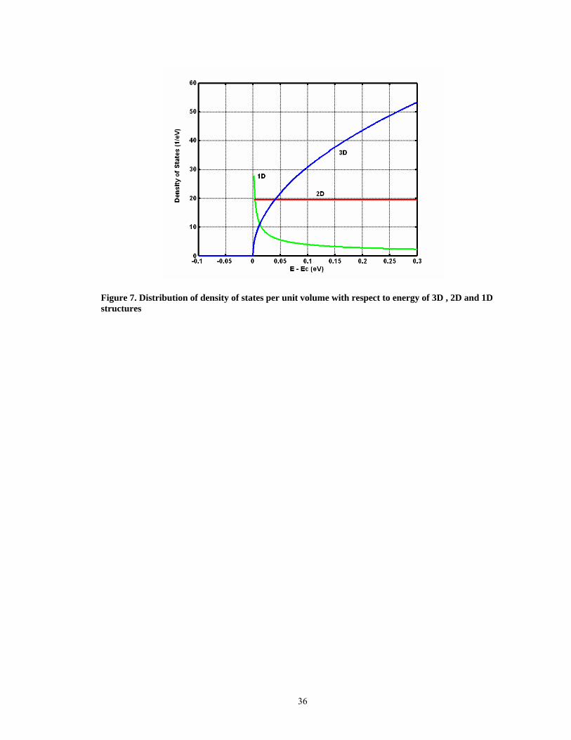
Figure 7. Distribution of density of states per unit volume with respect to energy of 3D , 2D and 1D structures
36
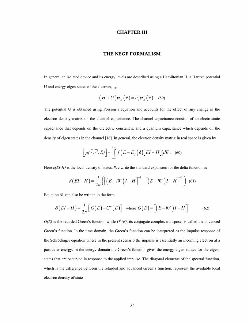
CHAPTER III
THE NEGF FORMALISM
In general an isolated device and its energy levels are described using a Hamiltonian H, a Hartree potential
U and energy eigen-states of the electron, εα.
( ) ( ) ( )H U rα α αψ ε ψ+ = r (59)
The potential U is obtained using Poisson’s equation and accounts for the effect of any change in the
electron density matrix on the channel capacitance. The channel capacitance consists of an electrostatic
capacitance that depends on the dielectric constant εr and a quantum capacitance which depends on the
density of eigen states in the channel [16]. In general, the electron density matrix in real space is given by
( ) [ ](+
f )ρ( r ,r';E) = f E E δ EI H dE∞
−∞
⎡ ⎤ − −⎣ ⎦ ∫ . (60)
Here δ(EI-H) is the local density of states. We write the standard expansion for the delta function as
( ) ( ) ( )1 10 0
2iEI H E i I H E i I Hδπ
− −+ +⎛ ⎞⎡ ⎤ ⎡ ⎤− = + − − − −⎜ ⎟⎣ ⎦ ⎣ ⎦⎝ ⎠
(61)
Equation 61 can also be written in the form
( ) ( ) ( )2iEI H G E G Eδπ
+⎡ ⎤− = −⎣ ⎦ where ( ) ( ) 10G E E i I H
−+⎡ ⎤= − −⎣ ⎦ (62)
G(E) is the retarded Green’s function while G+(E), its conjugate complex transpose, is called the advanced
Green’s function. In the time domain, the Green’s function can be interpreted as the impulse response of
the Schrödinger equation where in the present scenario the impulse is essentially an incoming electron at a
particular energy. In the energy domain the Green’s function gives the energy eigen-values for the eigen-
states that are occupied in response to the applied impulse. The diagonal elements of the spectral function,
which is the difference between the retarded and advanced Green’s function, represent the available local
electron density of states.
37
( ) ( ) ( ) ( )', ; 2A r r E EI H G E G Eπδ +⎡ ⎤= − = −⎣ ⎦ (63)
The electron density in the channel is the product of the Fermi function and the available density of states
and for an isolated device is written as
( ) ( ) ( )', ;2fdEr r E f E E A Eρπ
+∞
−∞
⎡ ⎤= − ⎣ ⎦∫ (64)
The real portion of the diagonal elements of the density matrix, represent the electron density distribution in
the channel. This electron density represented as n is used in the Poisson’s equation to self-consistently
solve for the potential in the channel where Nd is the donor density and εr is the permittivity of the channel.
(2d
r
qU Nε
)n∇ = − − (65)
Figure 8. (a) Single energy level of an isolated channel (b) Broadening of electron energy levels in the channel when connected to contacts
To understand the process of current flow, consider an isolated device having a single energy level ε as
seen in figure 8a. The source and drain contacts have an infinite distribution of electronic energy states.
When the isolated device with single energy level ε is connected to the source and drain contacts, some of
the density of states around this energy level ε will spill over from the contacts into the channel. This
process is known as energy level broadening and is shown in figure 8b. Since the Fermi levels in the source
and drain are equal, the amount of broadening will be equal on both sides and hence the net current flow in
38
the channel will be zero. When a positive bias is applied on the drain side, the Fermi level on the drain side
is lowered according to equation 66, opening up states below the channel energy level ε in the drain.
2 1f f DE E qV= − (66)
The electrons entering the channel with energy ε now have states with lower energies available in the drain
to escape to. This causes the channel current to become non-zero. As the applied bias is increased linearly,
more and more states between ε and εf2 become available to remove electrons from the channel causing the
source to increase its supply of electrons into the channel. This phenomenon results in a linear increase of
current in the channel. Eventually, the difference in the channel energy level ε and the drain Fermi level εf2
is so great that there are no additional states around the energy ε in the drain for the channel electrons to
escape. The current reaches saturation such that the number of electrons leaving the drain will equal the
number of electrons entering from the source. This process also explains why experimental measurements
[85] have shown that the maximum measured conductance of a one-energy level channel approaches a
limiting value G0= 2q2/ ħ = 51.6(KΩ)-1.The above analogy of a one-energy level system is applicable to
nanoscale thin films and wires where available energy levels along the confined dimension are very limited
in addition to being spaced far apart from adjacent energy levels.
In the NEGF formalism the coupling of the device to the source and drain contacts is described using self-
energy matrices Σ1 and Σ2. The self-energy term can be viewed as a modification to the Hamiltonian to
incorporate the boundary conditions. Accordingly, equation 59 and 62 can be rewritten as
( ) ( ) ( )1 2H U rα α αψ ε ψ+ + ∑ + ∑ = r (67)
( ) ( ) 1
1 20G E E i I H−
+⎡ ⎤= − − − ∑ − ∑⎣ ⎦ (68)
The self-energy terms Σ1 and Σ2 originate from the solution of the contact Hamiltonian. In this semi-infinite
system, which is connected to the channel, there will be an incident wave from the channel as well as a
reflected wave from the contact. The wave function at the interface is matched to conserve energy resulting
in the boundary condition,
39
( )expj t ik a∑ = − j (69)
where t, the inter-unit coupling energy resulting from the discretization is given by
2
* 22t
m a= . (70)
Here kj corresponds to the wave vector of the electron entering from the channel while a corresponds to the
grid spacing that will be discussed later in this chapter. The broadening of the energy levels introduced by
connecting the device to the source and drain contacts is incorporated through the Gamma functions Γ1 and
Γ2 given by
( )1 1i 1+Γ = ∑ − ∑ and ( )2 2i 2
+Γ = ∑ − ∑ (71)
The self-energy terms affect the Hamiltonian in two ways. The real part of the self-energy term shifts the
device eigenstates or energy level while the imaginary part of Σ causes the density of states to broaden
while giving the eigenstates a finite lifetime. The electron density for the open system is now given by
[ ] ( )2
n dEG Eρπ
+∞
−∞
⎛⎡ ⎤= ⎜⎣ ⎦ ⎝ ⎠∫⎞⎟ (72)
Gn(E) represents the electron density per unit energy and is given by
( ) ( ) ( ) ( )n inG E G E E G E+= ∑ where ( ) ( ) ( )1 1 2in
2E E f E f⎡ ⎤ ⎡ ⎤ ⎡ ⎤∑ = Γ + Γ⎣ ⎦ ⎣ ⎦⎣ ⎦ (73)
For plane wave basis functions, the current through the channel is calculated as the difference between the
inflow and the outflow at any given contact.
nj j j
qjI trace A f trace G
∞
−∞
⎡ ⎤⎡ ⎤= − Γ − Γ⎣ ⎦ ⎣ ⎦∫ (74)
where the subscript j indexes the contacts. For a two-terminal device I1 = −I2.
Two kinds of devices are examined in the present work as shown in figure 9. The first is a 2D film with
infinite dimensions along the x and y axes (perpendicular to the current flow) while the thickness along the
z axis (in the direction of current flow) has nanoscale dimensions (few nanometers). The second device is a
nanowire with infinite length in the x direction, while the y and z directions have reduced dimensions.
Electrical bias is applied along the confined z direction in the cases of both film and wire. Doping in the
40
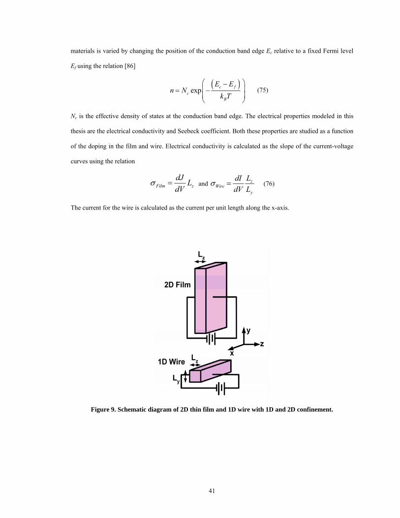
materials is varied by changing the position of the conduction band edge Ec relative to a fixed Fermi level
Ef using the relation [86]
( )
exp c fc
B
E En N
k T
⎛ ⎞−⎜ ⎟= −⎜ ⎟⎝ ⎠
(75)
Nc is the effective density of states at the conduction band edge. The electrical properties modeled in this
thesis are the electrical conductivity and Seebeck coefficient. Both these properties are studied as a function
of the doping in the film and wire. Electrical conductivity is calculated as the slope of the current-voltage
curves using the relation
Film zdJ LdV
σ = and zWire
y
LdIdV L
σ = (76)
The current for the wire is calculated as the current per unit length along the x-axis.
Figure 9. Schematic diagram of 2D thin film and 1D wire with 1D and 2D confinement.
41
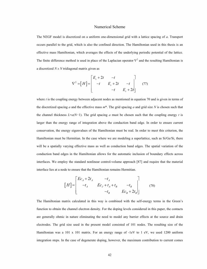
Numerical Scheme
The NEGF model is discretized on a uniform one-dimensional grid with a lattice spacing of a. Transport
occurs parallel to the grid, which is also the confined direction. The Hamiltonian used in this thesis is an
effective mass Hamiltonian, which averages the effects of the underlying periodic potential of the lattice.
The finite difference method is used in place of the Laplacian operator ∇2 and the resulting Hamiltonian is
a discretized N x N tridiagonal matrix given as
[ ]2
22
2
c
c
c
E t tH t E t t
t E t
+ −⎡ ⎤⎢ ⎥∇ = = − + −⎢ ⎥⎢ ⎥− +⎣ ⎦
(77)
where t is the coupling energy between adjacent nodes as mentioned in equation 70 and is given in terms of
the discretized spacing a and the effective mass m*. The grid spacing a and grid size N is chosen such that
the channel thickness L=a(N−1). The grid spacing a must be chosen such that the coupling energy t is
larger than the energy range of integration above the conduction band edge. In order to ensure current
conservation, the energy eigenvalues of the Hamiltonian must be real. In order to meet this criterion, the
Hamiltonian must be Hermitian. In the case where we are modeling a superlattice, such as Si/Ge/Si, there
will be a spatially varying effective mass as well as conduction band edges. The spatial variation of the
conduction band edges in the Hamiltonian allows for the automatic inclusion of boundary effects across
interfaces. We employ the standard nonlinear control-volume approach [87] and require that the material
interface lies at a node to ensure that the Hamiltonian remains Hermitian.
[ ]2
2
A A A
A J A B B
B B B
Ec t tH t Ec t t t
t Ec
+ −⎡ ⎤⎢ ⎥= − + + −⎢ ⎥⎢ ⎥− +⎣ ⎦t
(78)
The Hamiltonian matrix calculated in this way is combined with the self-energy terms in the Green’s
function to obtain the channel electron density. For the doping levels considered in this paper, the contacts
are generally ohmic in nature eliminating the need to model any barrier effects at the source and drain
electrodes. The grid size used in the present model consisted of 101 nodes. The resulting size of the
Hamiltonian was a 101 x 101 matrix. For an energy range of -1eV to 1 eV, we used 1200 uniform
integration steps. In the case of degenerate doping, however, the maximum contribution to current comes
42
from energy values concentrated near the conduction band edge. In this case, care must be taken to choose
an energy range close to the conduction band edge to ensure that the contribution from those energy steps is
properly included. The matrix inversion in the Green’s function was performed for each integration step,
and the integration was performed self-consistently with the potential. This process was repeated for each
voltage in the calculated I-V characteristics. To ensure numerical accuracy, first the number of integration
steps was selected to ensure a suitable error. Next convergence of the potential calculation was set to an
acceptable error. A relaxation of 0.2–0.5 on the density usually allowed convergence in about 10 iterations.
The self-consistent approach can be used as long as the value of Uo (Uo =q2/εoεr) as well as the value of the
broadening Γ is comparable to kBT. If Uo exceeds kBT, the channel goes into the Coulomb blockade regime
where the self-consistent method cannot be used anymore to solve for potential. The coupling energy t also
has a similar effect as broadening and ensuring that t ≥ Uo will keep the channel in the self-consistent field
regime. A large t implies that the grid spacing a is small, leading to more delocalization of the electron
wave function, which, in turn, improves the accuracy of the self-consistent field calculation.
Calculation of Subband Currents
As mentioned in chapter 1, the electrons in a 2D film can be treated as having infinite range of energies
along the x and y axis while being confined along the z-axis which is also the direction of transport.
22 22 2 2
* * *( )2 2 2
yxc
x y z z
kk nE k Em m m L
π⎛ ⎞= + + + ⎜ ⎟
⎝ ⎠where n = 1, 2, 3……. (79)
The term zz
nk Lπ= is the wave vector corresponding to the confined electrons that form discrete standing
waves when confined in an infinite potential well and n is the subband index. For the film we use the 2D
Fermi function given in equation 11 that accounts for the infinite states along the x-y plane. Hence, along
the transport direction, the electron energy is written as
22
*( )2c
z z
nE k Em L
π⎛ ⎞= + ⎜ ⎟
⎝ ⎠ (80)
43
In the NEGF formalism, the energy of each subband is obtained directly by solving for the Eigen values of
the Hamiltonian [H]. The conduction band and subsequent subbands are treated as individual, single-energy
channels. In the case of ballistic transport where there is no scattering between energy levels, this approach
allows us to model electron transport in the device separately for each energy level. Accordingly, current-
voltage characteristics are obtained for the conduction band and each additional subband separately. The
current thus obtained is summed over all the bands to obtain the net channel current. We start by writing
the Schrödinger wave equation along the z-axis as
[ ] nz nz nzH ψ ε ψ= (81)
The electron energies along the z-axis can be obtained by substituting a plane wave basis for the electron
wave function in the Hamiltonian and solving the Schrödinger wave equation along the z-axis using the
finite-difference method.
( )( )( ) 2 1 cosn z c nzk E t k aε = + − (82)
When solved in this way, the value of kz for an isolated channel will be equal to nπ/Lz corresponding to
standing waves in the channel. When the channel is connected to the contacts, some of the energy density
states from the infinite contacts spill over into the channel broadening the energy levels around each energy
band in the channel. The wave vectors associated with the broadened energy levels around each band can
be obtained by solving the energy conservation equation. For example, the wave vectors corresponding to
the broadened energy states around the conduction band Ec are
1cos 12
cz
E Ek at
− −⎡ ⎤= −⎢ ⎥⎣ ⎦ (83)
Similarly, wave vectors for broadened states around the first subband are obtained as
1 1cos 12
subz
E Ek at
− −⎡ ⎤= −⎢ ⎥⎣ ⎦ and so on. (84)
For each energy band, the channel current-voltage characteristics are obtained independently until the
contribution by any additional subbands is negligible. The final channel current at a particular voltage is
obtained as the sum of the currents of the conduction band and the contributing subbands.
44
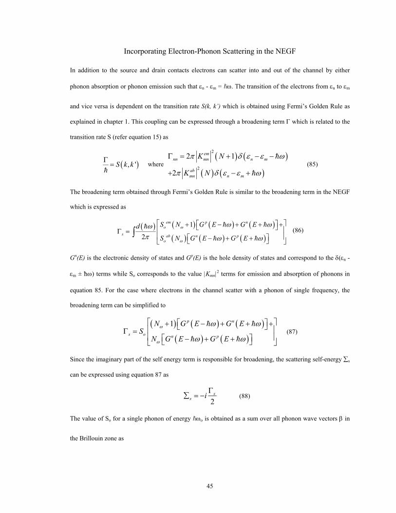
Incorporating Electron-Phonon Scattering in the NEGF
In addition to the source and drain contacts electrons can scatter into and out of the channel by either
phonon absorption or phonon emission such that εn - εm = ω. The transition of the electrons from εn to εm
and vice versa is dependent on the transition rate S(k, k’) which is obtained using Fermi’s Golden Rule as
explained in chapter 1. This coupling can be expressed through a broadening term Γ which is related to the
transition rate S (refer equation 15) as
( , 'S k kΓ= ) where
( ) ( )
( ) ( )
2
2
2 1
2
emnn mn n m
abmn n m
K N
K N
π δ ε ε ω
π δ ε ε ω
Γ = + − −
+ − + (85)
The broadening term obtained through Fermi’s Golden Rule is similar to the broadening term in the NEGF
which is expressed as
( ) ( ) ( ) ( )( ) ( ) ( )
1
2
em p no
s ab n po
S N G E G Ed
S N G E G E
ω
ω
ω ωωπ ω ω
⎡ ⎤⎡ ⎤+ − + + +⎣ ⎦⎢ ⎥Γ =⎢ ⎥⎡ ⎤− + +⎣ ⎦⎣ ⎦
∫ (86)
Gn(E) is the electronic density of states and Gp(E) is the hole density of states and correspond to the δ(εn -
εm ± ħω) terms while So corresponds to the value |Kmn|2 terms for emission and absorption of phonons in
equation 85. For the case where electrons in the channel scatter with a phonon of single frequency, the
broadening term can be simplified to
( ) ( ) ( )( ) ( )
1 p n
s o n p
N G E G ES
N G E G E
ω
ω
ω ω
ω ω
⎡ ⎤⎡ ⎤+ − + + +⎣ ⎦⎢ ⎥Γ =⎢ ⎥⎡ ⎤− + +⎣ ⎦⎣ ⎦
(87)
Since the imaginary part of the self energy term is responsible for broadening, the scattering self-energy ∑s
can be expressed using equation 87 as
2
ss i Γ
∑ = − (88)
The value of So for a single phonon of energy ωo is obtained as a sum over all phonon wave vectors β in
the Brillouin zone as
45
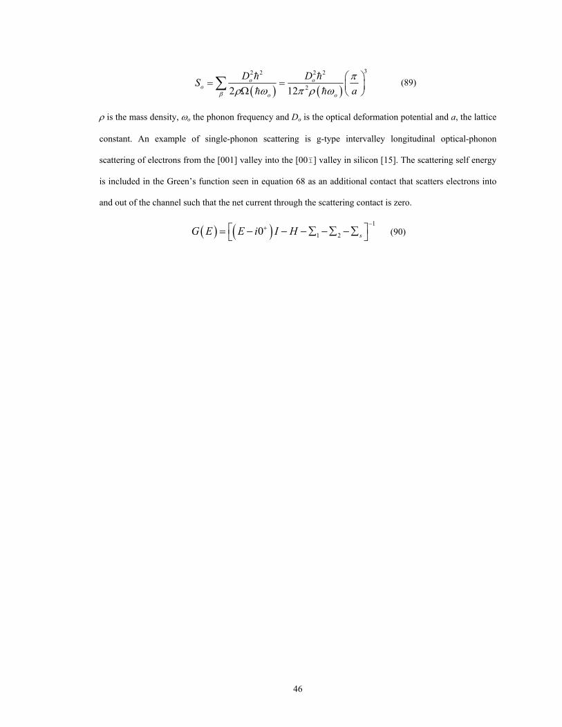
( ) ( )
32 2 2 2
22 12o o
oo o
D DSaβ
πρ ω π ρ ω
⎛ ⎞= = ⎜ ⎟Ω ⎝ ⎠∑ (89)
ρ is the mass density, ωo the phonon frequency and Do is the optical deformation potential and a, the lattice
constant. An example of single-phonon scattering is g-type intervalley longitudinal optical-phonon
scattering of electrons from the [001] valley into the [00§] valley in silicon [15]. The scattering self energy
is included in the Green’s function seen in equation 68 as an additional contact that scatters electrons into
and out of the channel such that the net current through the scattering contact is zero.
( ) ( ) 1
1 20 sG E E i I H−
+⎡ ⎤= − − − ∑ − ∑ − ∑⎣ ⎦ (90)
46
CHAPTER IV
RESULTS FOR SILICON NANO-FILMS AND NANO-WIRES
The NEGF method is used to calculate the current density of silicon films for varying thickness under a
constant applied field of 106 V/m. The current density is for each film is calculated for two cases 1) ballistic
electron transport through the film and 2) electrons scattering with longitudinal optical phonons. The results
are shown in figure 10 and demonstrate the three fundamental aspects of electron transport in nanoscale
devices. The calculated current is very small for small film thicknesses and increases as the film thickness
increases. This is the effect of electron confinement where very small film thickness leads to the formation
of discrete subband energies that are spaced far apart in the energy space of the Brillouin zone. The
electrons in thin films have very limited number of subbands available for transport leading to low current
density.
The second important effect is the impact of electron-phonon scattering on the current density. Scattering in
the NEGF model is included such that electrons scatter within the broadened energy levels at each energy
band. Intersubband scattering is not modeled in this research. Since very small films have limited subbands
that contribute to current flow, the effect of scattering is also limited to very few subbands. As a result, the
effect of scattering is less than 10% for film thicknesses up to 5nm. As the film thickness increases, the
subband energies are spaced closer to each other leading to increased contribution to current flow. In
addition the subbands are also lower in energy as they come closer to the conduction band edge As a result,
there is a higher probability for the electrons to scatter that begins to gain significance for film thicknesses
greater than 5nm where the decrease in current is now 12% of the ballistic current.
The limited impact of scattering on the current demonstrates the third important effect i.e. the
nonequilibrium nature of electron transport in silicon films with thicknesses equal to or less than 5nm to
7nm. Scattering with phonons is a way of restoring equilibrium in a system. If the electrons experience very
47
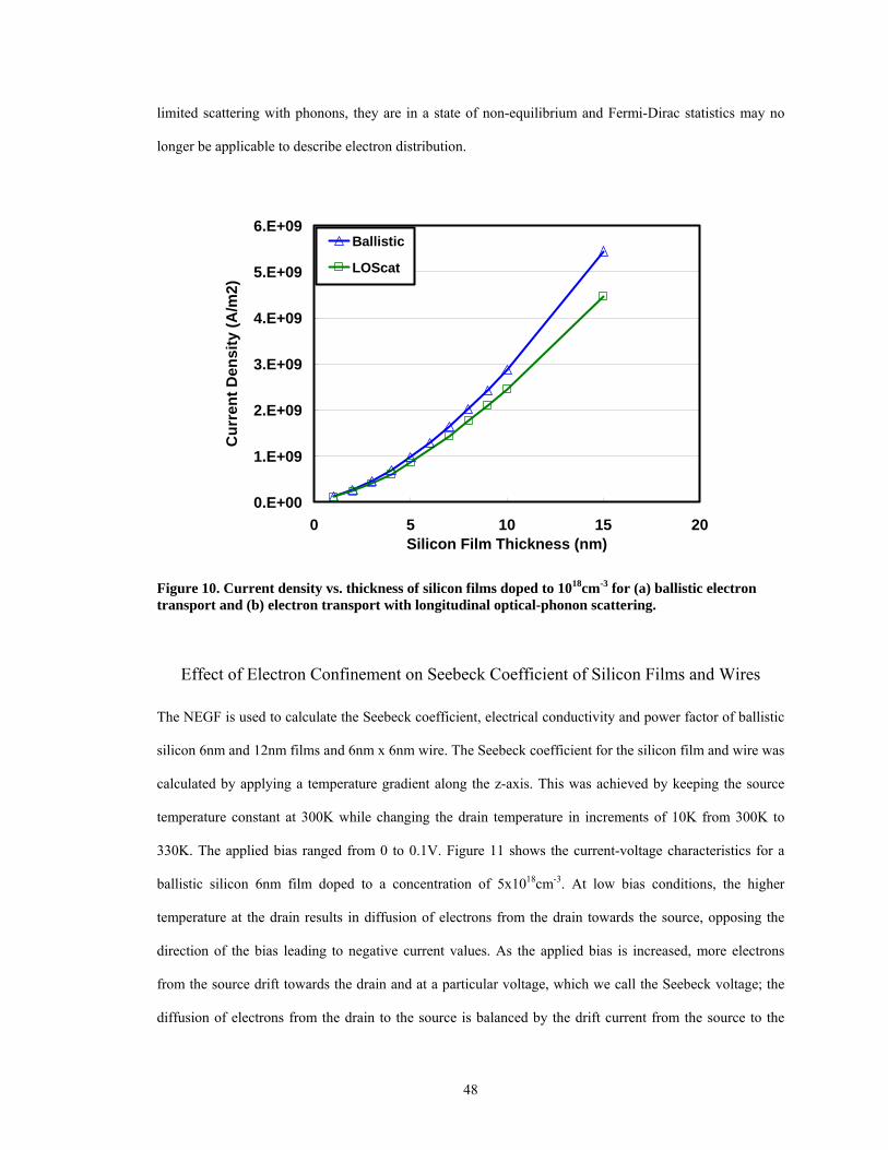
limited scattering with phonons, they are in a state of non-equilibrium and Fermi-Dirac statistics may no
longer be applicable to describe electron distribution.
0.E+00
1.E+09
2.E+09
3.E+09
4.E+09
5.E+09
6.E+09
0 5 10 15 20Silicon Film Thickness (nm)
Cur
rent
Den
sity
(A/m
2)Ballistic
LOScat
Figure 10. Current density vs. thickness of silicon films doped to 1018cm-3 for (a) ballistic electron transport and (b) electron transport with longitudinal optical-phonon scattering.
Effect of Electron Confinement on Seebeck Coefficient of Silicon Films and Wires
The NEGF is used to calculate the Seebeck coefficient, electrical conductivity and power factor of ballistic
silicon 6nm and 12nm films and 6nm x 6nm wire. The Seebeck coefficient for the silicon film and wire was
calculated by applying a temperature gradient along the z-axis. This was achieved by keeping the source
temperature constant at 300K while changing the drain temperature in increments of 10K from 300K to
330K. The applied bias ranged from 0 to 0.1V. Figure 11 shows the current-voltage characteristics for a
ballistic silicon 6nm film doped to a concentration of 5x1018cm-3. At low bias conditions, the higher
temperature at the drain results in diffusion of electrons from the drain towards the source, opposing the
direction of the bias leading to negative current values. As the applied bias is increased, more electrons
from the source drift towards the drain and at a particular voltage, which we call the Seebeck voltage; the
diffusion of electrons from the drain to the source is balanced by the drift current from the source to the
48
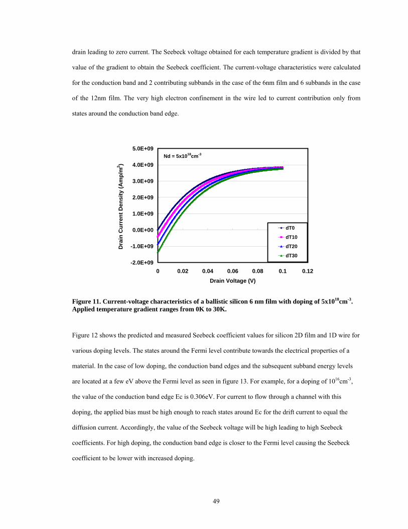
drain leading to zero current. The Seebeck voltage obtained for each temperature gradient is divided by that
value of the gradient to obtain the Seebeck coefficient. The current-voltage characteristics were calculated
for the conduction band and 2 contributing subbands in the case of the 6nm film and 6 subbands in the case
of the 12nm film. The very high electron confinement in the wire led to current contribution only from
states around the conduction band edge.
-2.0E+09
-1.0E+09
0.0E+00
1.0E+09
2.0E+09
3.0E+09
4.0E+09
5.0E+09
0 0.02 0.04 0.06 0.08 0.1 0.12Drain Voltage (V)
Dra
in C
urre
nt D
ensi
ty (A
mp/
m2 )
dT0
dT10
dT20
dT30
Nd = 5x1018cm-3
Figure 11. Current-voltage characteristics of a ballistic silicon 6 nm film with doping of 5x1018cm-3. Applied temperature gradient ranges from 0K to 30K.
Figure 12 shows the predicted and measured Seebeck coefficient values for silicon 2D film and 1D wire for
various doping levels. The states around the Fermi level contribute towards the electrical properties of a
material. In the case of low doping, the conduction band edges and the subsequent subband energy levels
are located at a few eV above the Fermi level as seen in figure 13. For example, for a doping of 1016cm-3,
the value of the conduction band edge Ec is 0.306eV. For current to flow through a channel with this
doping, the applied bias must be high enough to reach states around Ec for the drift current to equal the
diffusion current. Accordingly, the value of the Seebeck voltage will be high leading to high Seebeck
coefficients. For high doping, the conduction band edge is closer to the Fermi level causing the Seebeck
coefficient to be lower with increased doping.
49
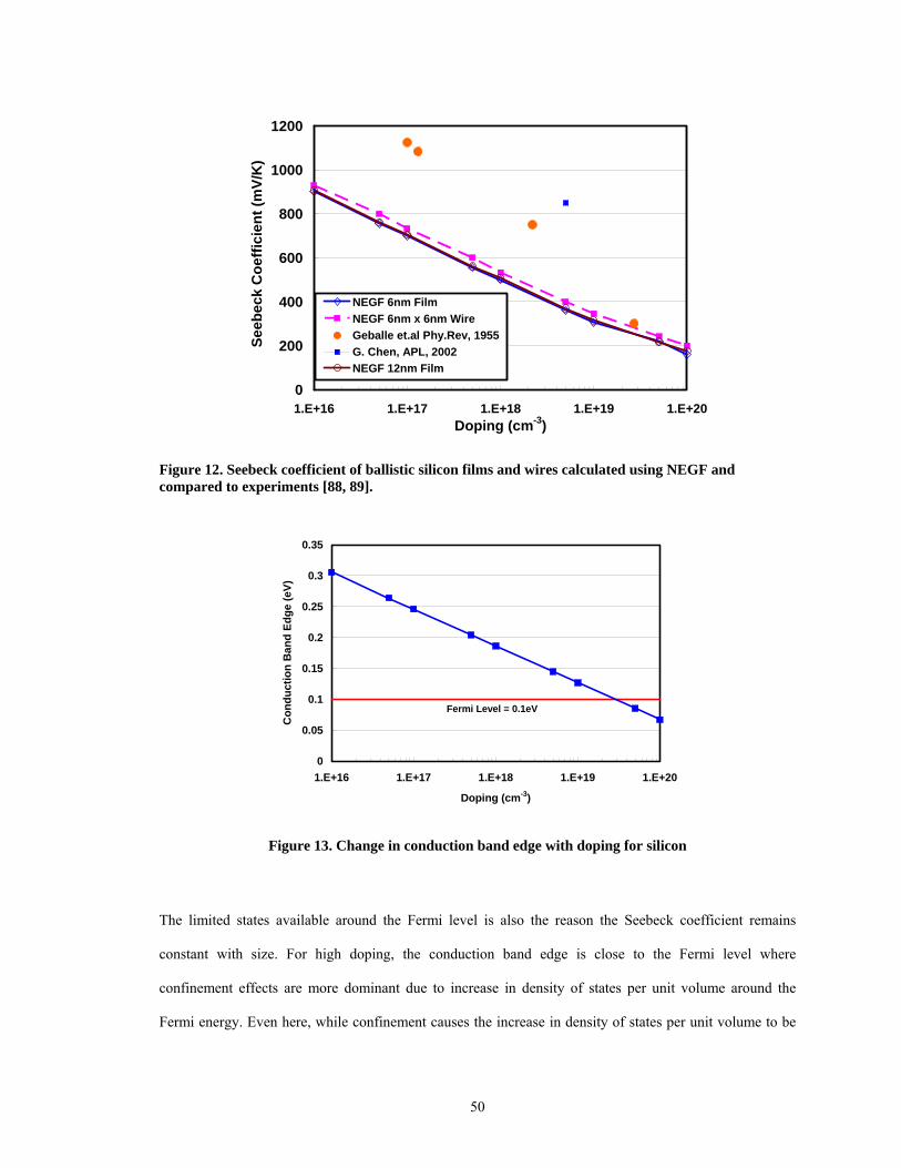
0
200
400
600
800
1000
1200
1.E+16 1.E+17 1.E+18 1.E+19 1.E+20Doping (cm-3)
Seeb
eck
Coe
ffici
ent (
mV/
K)
NEGF 6nm FilmNEGF 6nm x 6nm WireGeballe et.al Phy.Rev, 1955G. Chen, APL, 2002NEGF 12nm Film
Figure 12. Seebeck coefficient of ballistic silicon films and wires calculated using NEGF and compared to experiments [88, 89].
0
0.05
0.1
0.15
0.2
0.25
0.3
0.35
1.E+16 1.E+17 1.E+18 1.E+19 1.E+20
Doping (cm-3)
Con
duct
ion
Ban
d Ed
ge (e
V)
Fermi Level = 0.1eV
Figure 13. Change in conduction band edge with doping for silicon
The limited states available around the Fermi level is also the reason the Seebeck coefficient remains
constant with size. For high doping, the conduction band edge is close to the Fermi level where
confinement effects are more dominant due to increase in density of states per unit volume around the
Fermi energy. Even here, while confinement causes the increase in density of states per unit volume to be
50
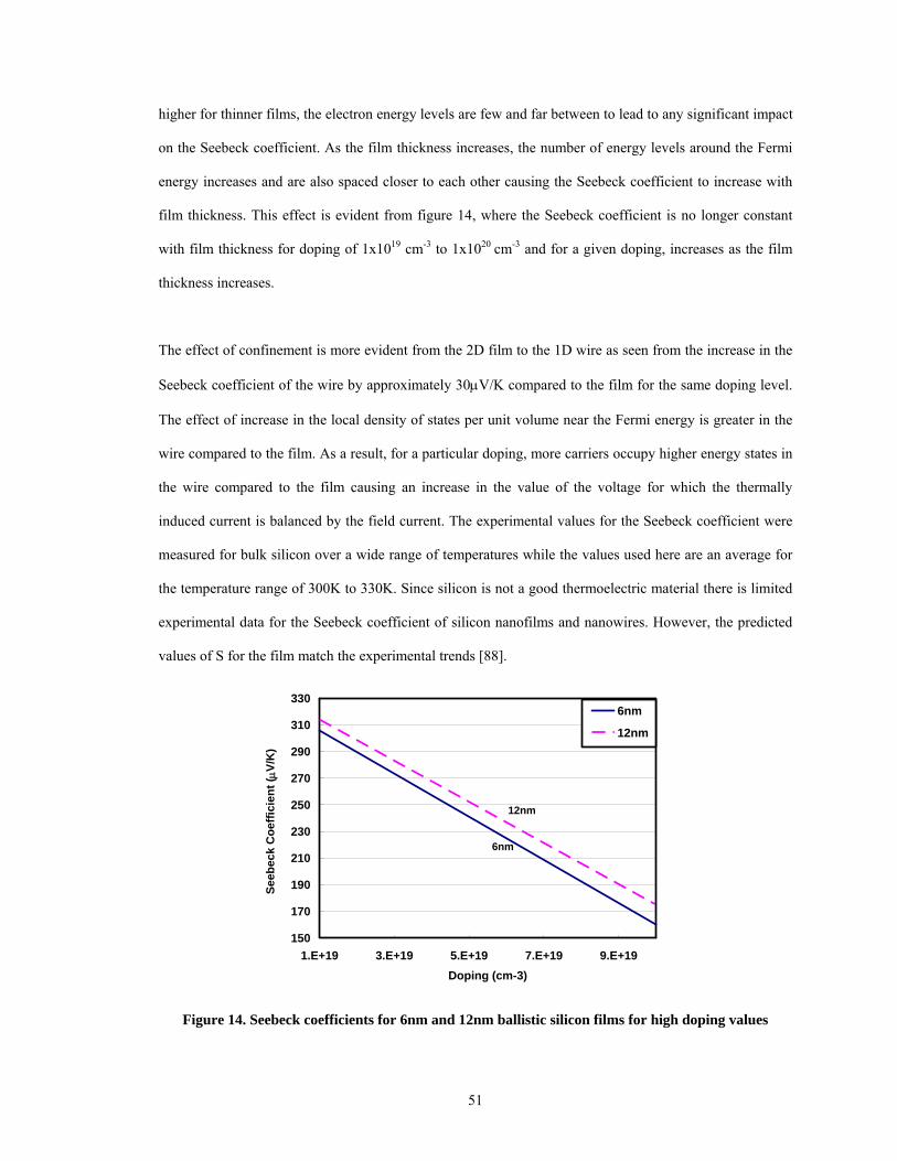
higher for thinner films, the electron energy levels are few and far between to lead to any significant impact
on the Seebeck coefficient. As the film thickness increases, the number of energy levels around the Fermi
energy increases and are also spaced closer to each other causing the Seebeck coefficient to increase with
film thickness. This effect is evident from figure 14, where the Seebeck coefficient is no longer constant
with film thickness for doping of 1x1019 cm-3 to 1x1020 cm-3 and for a given doping, increases as the film
thickness increases.
The effect of confinement is more evident from the 2D film to the 1D wire as seen from the increase in the
Seebeck coefficient of the wire by approximately 30µV/K compared to the film for the same doping level.
The effect of increase in the local density of states per unit volume near the Fermi energy is greater in the
wire compared to the film. As a result, for a particular doping, more carriers occupy higher energy states in
the wire compared to the film causing an increase in the value of the voltage for which the thermally
induced current is balanced by the field current. The experimental values for the Seebeck coefficient were
measured for bulk silicon over a wide range of temperatures while the values used here are an average for
the temperature range of 300K to 330K. Since silicon is not a good thermoelectric material there is limited
experimental data for the Seebeck coefficient of silicon nanofilms and nanowires. However, the predicted
values of S for the film match the experimental trends [88].
150
170
190
210
230
250
270
290
310
330
1.E+19 3.E+19 5.E+19 7.E+19 9.E+19Doping (cm-3)
Seeb
eck
Coe
ffici
ent (
µV/K
)
6nm
12nm
12nm
6nm
Figure 14. Seebeck coefficients for 6nm and 12nm ballistic silicon films for high doping values
51
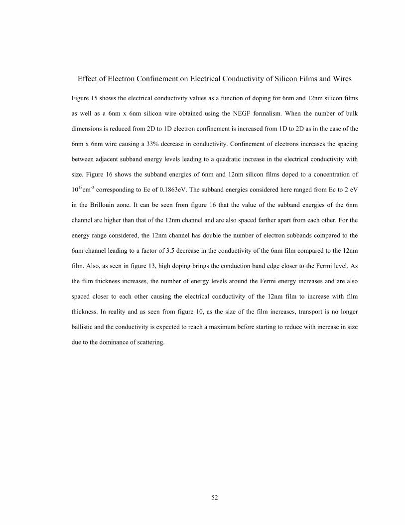
Effect of Electron Confinement on Electrical Conductivity of Silicon Films and Wires
Figure 15 shows the electrical conductivity values as a function of doping for 6nm and 12nm silicon films
as well as a 6nm x 6nm silicon wire obtained using the NEGF formalism. When the number of bulk
dimensions is reduced from 2D to 1D electron confinement is increased from 1D to 2D as in the case of the
6nm x 6nm wire causing a 33% decrease in conductivity. Confinement of electrons increases the spacing
between adjacent subband energy levels leading to a quadratic increase in the electrical conductivity with
size. Figure 16 shows the subband energies of 6nm and 12nm silicon films doped to a concentration of
1018cm-3 corresponding to Ec of 0.1863eV. The subband energies considered here ranged from Ec to 2 eV
in the Brillouin zone. It can be seen from figure 16 that the value of the subband energies of the 6nm
channel are higher than that of the 12nm channel and are also spaced farther apart from each other. For the
energy range considered, the 12nm channel has double the number of electron subbands compared to the
6nm channel leading to a factor of 3.5 decrease in the conductivity of the 6nm film compared to the 12nm
film. Also, as seen in figure 13, high doping brings the conduction band edge closer to the Fermi level. As
the film thickness increases, the number of energy levels around the Fermi energy increases and are also
spaced closer to each other causing the electrical conductivity of the 12nm film to increase with film
thickness. In reality and as seen from figure 10, as the size of the film increases, transport is no longer
ballistic and the conductivity is expected to reach a maximum before starting to reduce with increase in size
due to the dominance of scattering.
52
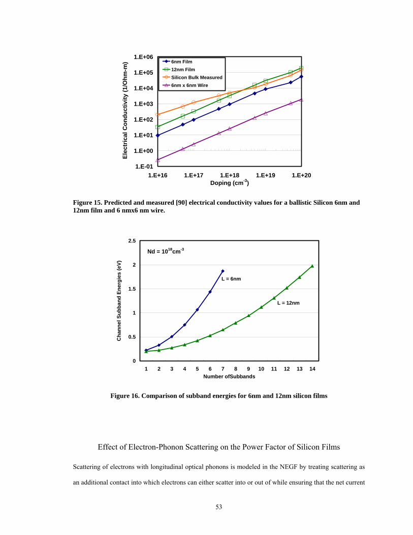
1.E-01
1.E+00
1.E+01
1.E+02
1.E+03
1.E+04
1.E+05
1.E+06
1.E+16 1.E+17 1.E+18 1.E+19 1.E+20Doping (cm-3)
Elec
tric
al C
ondu
ctiv
ity (1
/Ohm
-m) 6nm Film
12nm FilmSilicon Bulk Measured6nm x 6nm Wire
Figure 15. Predicted and measured [90] electrical conductivity values for a ballistic Silicon 6nm and 12nm film and 6 nmx6 nm wire.
0
0.5
1
1.5
2
2.5
1 2 3 4 5 6 7 8 9 10 11 12 13 14Number ofSubbands
Cha
nnel
Sub
band
Ene
rgie
s (e
V)
L = 6nm
L = 12nm
Nd = 1018cm-3
Figure 16. Comparison of subband energies for 6nm and 12nm silicon films
Effect of Electron-Phonon Scattering on the Power Factor of Silicon Films
Scattering of electrons with longitudinal optical phonons is modeled in the NEGF by treating scattering as
an additional contact into which electrons can either scatter into or out of while ensuring that the net current
53
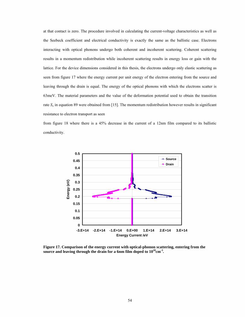
at that contact is zero. The procedure involved in calculating the current-voltage characteristics as well as
the Seebeck coefficient and electrical conductivity is exactly the same as the ballistic case. Electrons
interacting with optical phonons undergo both coherent and incoherent scattering. Coherent scattering
results in a momentum redistribution while incoherent scattering results in energy loss or gain with the
lattice. For the device dimensions considered in this thesis, the electrons undergo only elastic scattering as
seen from figure 17 where the energy current per unit energy of the electron entering from the source and
leaving through the drain is equal. The energy of the optical phonons with which the electrons scatter is
63meV. The material parameters and the value of the deformation potential used to obtain the transition
rate So in equation 89 were obtained from [15]. The momentum redistribution however results in significant
resistance to electron transport as seen
from figure 18 where there is a 45% decrease in the current of a 12nm film compared to its ballistic
conductivity.
0
0.05
0.1
0.15
0.2
0.25
0.3
0.35
0.4
0.45
0.5
-3.E+14 -2.E+14 -1.E+14 0.E+00 1.E+14 2.E+14 3.E+14Energy Current /eV
Ener
gy (e
V)
SourceDrain
Figure 17. Comparison of the energy current with optical-phonon scattering, entering from the source and leaving through the drain for a 6nm film doped to 1018cm-3.
54
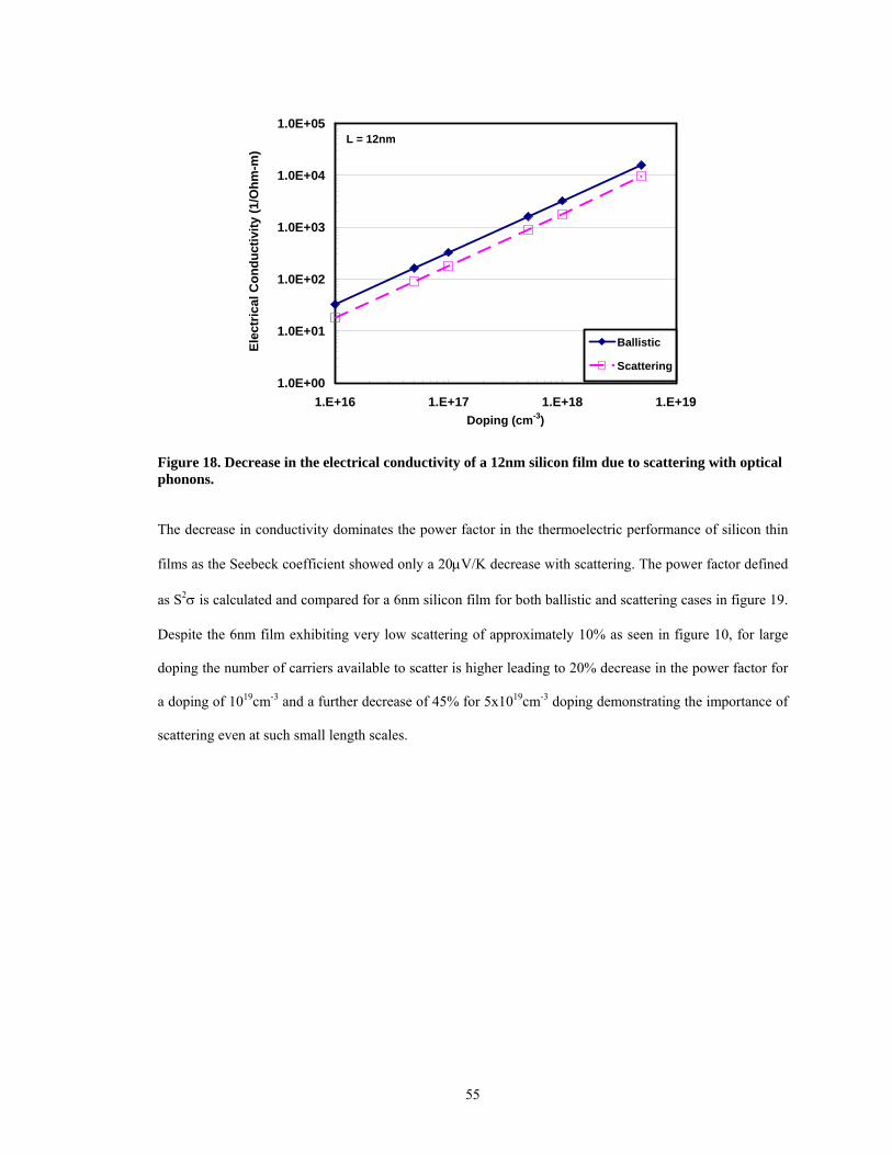
1.0E+00
1.0E+01
1.0E+02
1.0E+03
1.0E+04
1.0E+05
1.E+16 1.E+17 1.E+18 1.E+19Doping (cm-3)
Elec
tric
al C
ondu
ctiv
ity (1
/Ohm
-m)
Ballistic
Scattering
L = 12nm
Figure 18. Decrease in the electrical conductivity of a 12nm silicon film due to scattering with optical phonons.
The decrease in conductivity dominates the power factor in the thermoelectric performance of silicon thin
films as the Seebeck coefficient showed only a 20µV/K decrease with scattering. The power factor defined
as S2σ is calculated and compared for a 6nm silicon film for both ballistic and scattering cases in figure 19.
Despite the 6nm film exhibiting very low scattering of approximately 10% as seen in figure 10, for large
doping the number of carriers available to scatter is higher leading to 20% decrease in the power factor for
a doping of 1019cm-3 and a further decrease of 45% for 5x1019cm-3 doping demonstrating the importance of
scattering even at such small length scales.
55
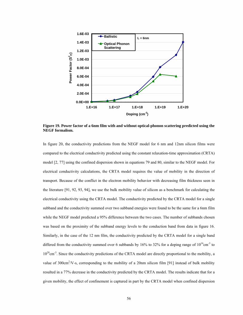
0.0E+00
2.0E-04
4.0E-04
6.0E-04
8.0E-04
1.0E-03
1.2E-03
1.4E-03
1.6E-03
1.E+16 1.E+17 1.E+18 1.E+19 1.E+20
Doping (cm-3)
Pow
er F
acto
r (S2 σ)
Ballistic
Optical PhononScattering
L = 6nm
Figure 19. Power factor of a 6nm film with and without optical-phonon scattering predicted using the NEGF formalism.
In figure 20, the conductivity predictions from the NEGF model for 6 nm and 12nm silicon films were
compared to the electrical conductivity predicted using the constant relaxation-time approximation (CRTA)
model [2, 77] using the confined dispersion shown in equations 79 and 80, similar to the NEGF model. For
electrical conductivity calculations, the CRTA model requires the value of mobility in the direction of
transport. Because of the conflict in the electron mobility behavior with decreasing film thickness seen in
the literature [91, 92, 93, 94], we use the bulk mobility value of silicon as a benchmark for calculating the
electrical conductivity using the CRTA model. The conductivity predicted by the CRTA model for a single
subband and the conductivity summed over two subband energies were found to be the same for a 6nm film
while the NEGF model predicted a 95% difference between the two cases. The number of subbands chosen
was based on the proximity of the subband energy levels to the conduction band from data in figure 16.
Similarly, in the case of the 12 nm film, the conductivity predicted by the CRTA model for a single band
differed from the conductivity summed over 6 subbands by 16% to 32% for a doping range of 1016cm-3 to
1020cm-3. Since the conductivity predictions of the CRTA model are directly proportional to the mobility, a
value of 300cm2/V-s, corresponding to the mobility of a 20nm silicon film [91] instead of bulk mobility
resulted in a 77% decrease in the conductivity predicted by the CRTA model. The results indicate that for a
given mobility, the effect of confinement is captured in part by the CRTA model when confined dispersion
56
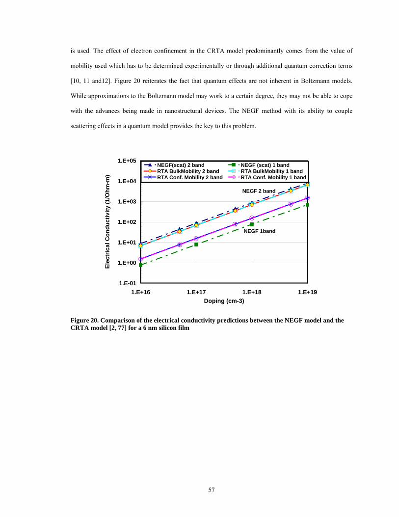
is used. The effect of electron confinement in the CRTA model predominantly comes from the value of
mobility used which has to be determined experimentally or through additional quantum correction terms
[10, 11 and12]. Figure 20 reiterates the fact that quantum effects are not inherent in Boltzmann models.
While approximations to the Boltzmann model may work to a certain degree, they may not be able to cope
with the advances being made in nanostructural devices. The NEGF method with its ability to couple
scattering effects in a quantum model provides the key to this problem.
1.E-01
1.E+00
1.E+01
1.E+02
1.E+03
1.E+04
1.E+05
1.E+16 1.E+17 1.E+18 1.E+19Doping (cm-3)
Elec
tric
al C
ondu
ctiv
ity (1
/Ohm
-m)
NEGF(scat) 2 band NEGF (scat) 1 bandRTA BulkMobility 2 band RTA BulkMobility 1 bandRTA Conf. Mobility 2 band RTA Conf. Mobility 1 band
NEGF 1band
NEGF 2 band
Figure 20. Comparison of the electrical conductivity predictions between the NEGF model and the CRTA model [2, 77] for a 6 nm silicon film
57
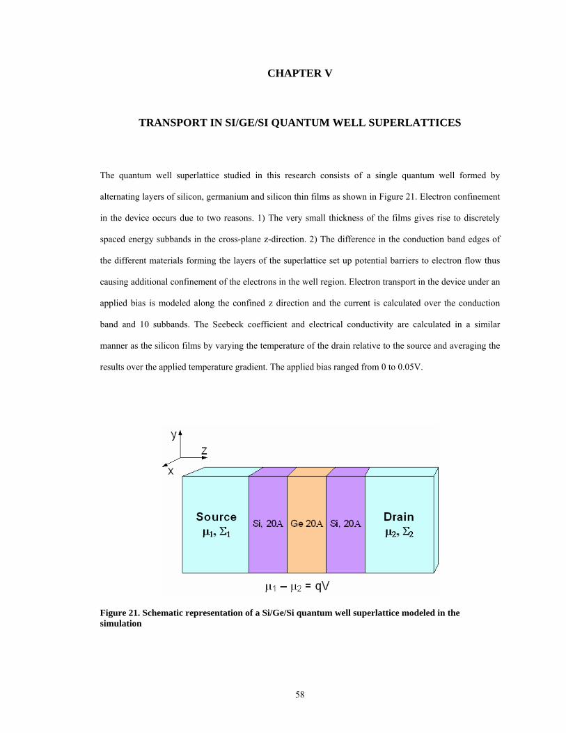
CHAPTER V
TRANSPORT IN SI/GE/SI QUANTUM WELL SUPERLATTICES
The quantum well superlattice studied in this research consists of a single quantum well formed by
alternating layers of silicon, germanium and silicon thin films as shown in Figure 21. Electron confinement
in the device occurs due to two reasons. 1) The very small thickness of the films gives rise to discretely
spaced energy subbands in the cross-plane z-direction. 2) The difference in the conduction band edges of
the different materials forming the layers of the superlattice set up potential barriers to electron flow thus
causing additional confinement of the electrons in the well region. Electron transport in the device under an
applied bias is modeled along the confined z direction and the current is calculated over the conduction
band and 10 subbands. The Seebeck coefficient and electrical conductivity are calculated in a similar
manner as the silicon films by varying the temperature of the drain relative to the source and averaging the
results over the applied temperature gradient. The applied bias ranged from 0 to 0.05V.
Figure 21. Schematic representation of a Si/Ge/Si quantum well superlattice modeled in the simulation
58
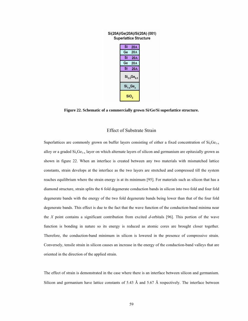
Figure 22. Schematic of a commercially grown Si/Ge/Si superlattice structure.
Effect of Substrate Strain
Superlattices are commonly grown on buffer layers consisting of either a fixed concentration of SixGe1-x
alloy or a graded SixGe1-x layer on which alternate layers of silicon and germanium are epitaxially grown as
shown in figure 22. When an interface is created between any two materials with mismatched lattice
constants, strain develops at the interface as the two layers are stretched and compressed till the system
reaches equilibrium where the strain energy is at its minimum [95]. For materials such as silicon that has a
diamond structure, strain splits the 6 fold degenerate conduction bands in silicon into two fold and four fold
degenerate bands with the energy of the two fold degenerate bands being lower than that of the four fold
degenerate bands. This effect is due to the fact that the wave function of the conduction-band minima near
the X point contains a significant contribution from excited d-orbitals [96]. This portion of the wave
function is bonding in nature so its energy is reduced as atomic cores are brought closer together.
Therefore, the conduction-band minimum in silicon is lowered in the presence of compressive strain.
Conversely, tensile strain in silicon causes an increase in the energy of the conduction-band valleys that are
oriented in the direction of the applied strain.
The effect of strain is demonstrated in the case where there is an interface between silicon and germanium.
Silicon and germanium have lattice constants of 5.43 Å and 5.67 Å respectively. The interface between
59
(001) silicon and (001) germanium surfaces produces biaxial tensile strain in the plane of the silicon lattice
due its smaller lattice constant. Accordingly, the silicon (001) layers will experience tensile biaxial strain in
the plane of the interface raising the energies of the (100) and (010) valleys in k-space. The compressive
stress generated in silicon along the [001] direction perpendicular to the plane of strain lowers the
conduction band valley in the ∆ direction in k-space. Similarly the germanium (001) atoms will experience
compressive biaxial strain leading to a decrease in the energy of the (100) and (010) valleys while the
energy of the (001) valley along the z-axis is increased due to tensile stress. Therefore, biaxial strain breaks
the symmetry that originally exists due to splitting of the conduction band minima.
In general, the effective mass for motion along an axis is higher than the effective mass in the plane
perpendicular to the axis. For example, in silicon, the effective mass for motion along the z axis or [001]
direction is 0.91me while the effective mass along the [100] and [010] axis is 0.19me leading to higher
mobility in the x-y plane. At room temperature, electrons lie predominantly in the valleys corresponding to
the x and y axes. Under biaxial strain, the energy minima of the z-axis is lowered and electrons fall into the
valley corresponding to the (001) valley which has lower effective mass in the x-y plane. This feature is
exploited in MOSFETS where the mobility along the x-y plane is higher for biaxial strain in the (001)
layers perpendicular to the z-axis. Since we are studying transport in the cross-plane direction of
superlattices, electron transport along the [001] direction is modeled using an effective mass of 0.91me.
During the fabrication of superlattice structures, the epitaxial growth of the various layers ensures that the
final lattice constant is equal to that of the corresponding substrate. For example, if the substrate used is
Si0.5Ge0.5 then the silicon and germanium layers are strained accordingly to match the lattice constant of
Si0.5Ge0.5. In this case the lattice constant of Si0.5Ge0.5 is 5.54 Å which is greater than the lattice constant of
silicon and lower than that of germanium. Accordingly, the conduction band minima in the silicon layers
will be lowered while the energy in germanium will increase. Van de Walle [97] in 1989 developed a
model-solid theory to calculate the change in the bandstructure of materials under biaxial strain. According
to his research, the shift in the conduction band with respect to the average value is given by
60
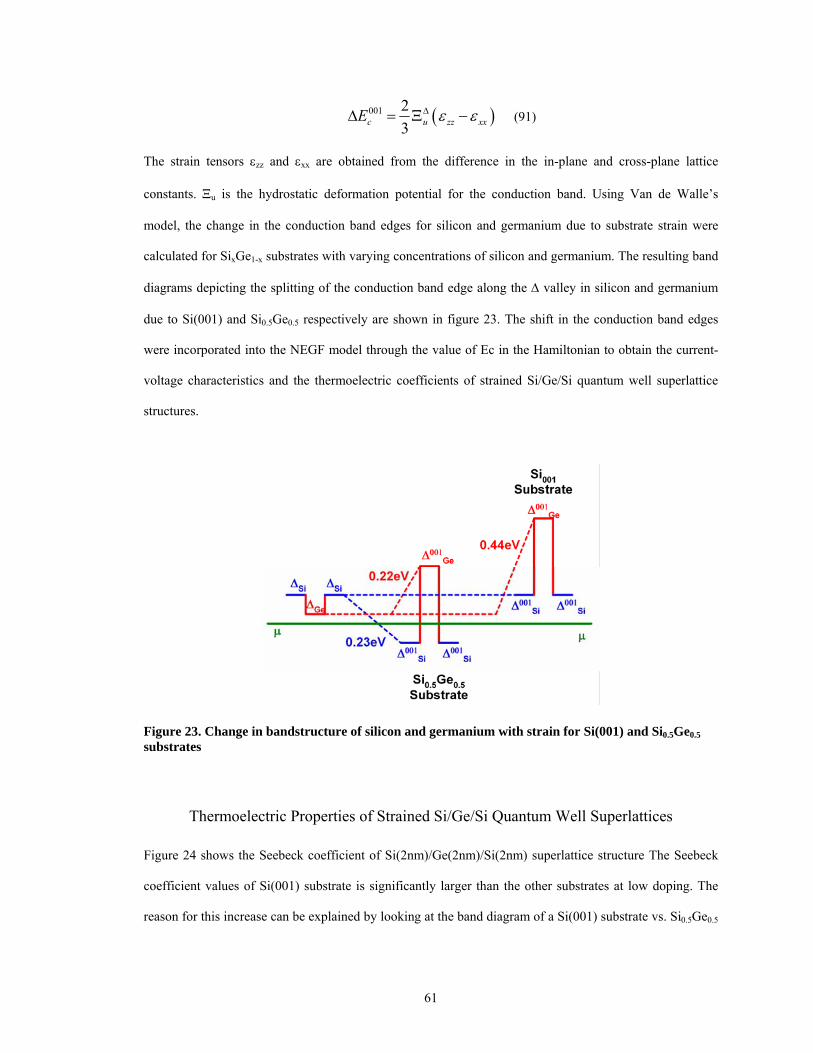
( )001 23c u zzE xxε ε∆∆ = Ξ − (91)
The strain tensors εzz and εxx are obtained from the difference in the in-plane and cross-plane lattice
constants. Ξu is the hydrostatic deformation potential for the conduction band. Using Van de Walle’s
model, the change in the conduction band edges for silicon and germanium due to substrate strain were
calculated for SixGe1-x substrates with varying concentrations of silicon and germanium. The resulting band
diagrams depicting the splitting of the conduction band edge along the ∆ valley in silicon and germanium
due to Si(001) and Si0.5Ge0.5 respectively are shown in figure 23. The shift in the conduction band edges
were incorporated into the NEGF model through the value of Ec in the Hamiltonian to obtain the current-
voltage characteristics and the thermoelectric coefficients of strained Si/Ge/Si quantum well superlattice
structures.
Figure 23. Change in bandstructure of silicon and germanium with strain for Si(001) and Si0.5Ge0.5 substrates
Thermoelectric Properties of Strained Si/Ge/Si Quantum Well Superlattices
Figure 24 shows the Seebeck coefficient of Si(2nm)/Ge(2nm)/Si(2nm) superlattice structure The Seebeck
coefficient values of Si(001) substrate is significantly larger than the other substrates at low doping. The
reason for this increase can be explained by looking at the band diagram of a Si(001) substrate vs. Si0.5Ge0.5
61
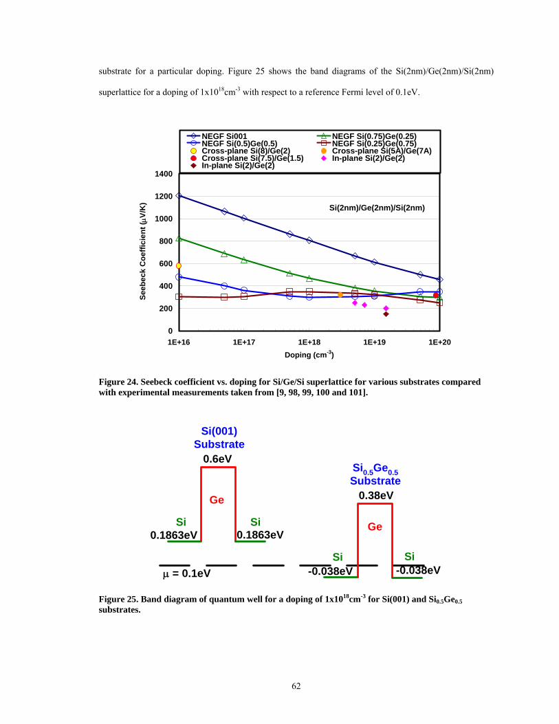
substrate for a particular doping. Figure 25 shows the band diagrams of the Si(2nm)/Ge(2nm)/Si(2nm)
superlattice for a doping of 1x1018cm-3 with respect to a reference Fermi level of 0.1eV.
0
200
400
600
800
1000
1200
1400
1E+16 1E+17 1E+18 1E+19 1E+20Doping (cm-3)
Seeb
eck
Coe
ffici
ent (
µV/K
)NEGF Si001 NEGF Si(0.75)Ge(0.25)NEGF Si(0.5)Ge(0.5) NEGF Si(0.25)Ge(0.75)Cross-plane Si(8)/Ge(2) Cross-plane Si(5A)/Ge(7A)Cross-plane Si(7.5)/Ge(1.5) In-plane Si(2)/Ge(2)In-plane Si(2)/Ge(2)
Si(2nm)/Ge(2nm)/Si(2nm)
Figure 24. Seebeck coefficient vs. doping for Si/Ge/Si superlattice for various substrates compared with experimental measurements taken from [9, 98, 99, 100 and 101].
0.1863eV
0.6eV
0.1863eV
Ge
Si Si
-0.038eV
0.38eV
-0.038eVSi Si
µ = 0.1eV
Si(001)Substrate
Si0.5Ge0.5Substrate
Ge
Figure 25. Band diagram of quantum well for a doping of 1x1018cm-3 for Si(001) and Si0.5Ge0.5 substrates.
62
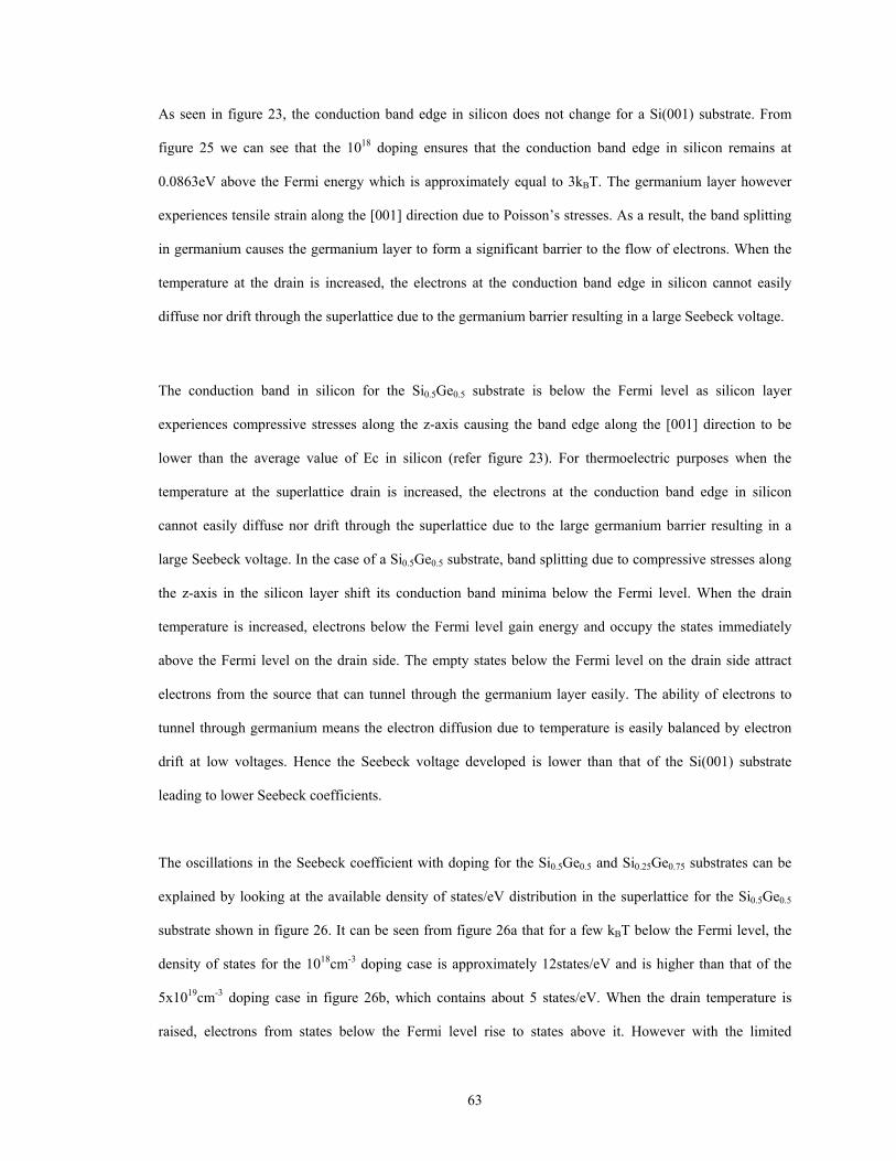
As seen in figure 23, the conduction band edge in silicon does not change for a Si(001) substrate. From
figure 25 we can see that the 1018 doping ensures that the conduction band edge in silicon remains at
0.0863eV above the Fermi energy which is approximately equal to 3kBT. The germanium layer however
experiences tensile strain along the [001] direction due to Poisson’s stresses. As a result, the band splitting
in germanium causes the germanium layer to form a significant barrier to the flow of electrons. When the
temperature at the drain is increased, the electrons at the conduction band edge in silicon cannot easily
diffuse nor drift through the superlattice due to the germanium barrier resulting in a large Seebeck voltage.
The conduction band in silicon for the Si0.5Ge0.5 substrate is below the Fermi level as silicon layer
experiences compressive stresses along the z-axis causing the band edge along the [001] direction to be
lower than the average value of Ec in silicon (refer figure 23). For thermoelectric purposes when the
temperature at the superlattice drain is increased, the electrons at the conduction band edge in silicon
cannot easily diffuse nor drift through the superlattice due to the large germanium barrier resulting in a
large Seebeck voltage. In the case of a Si0.5Ge0.5 substrate, band splitting due to compressive stresses along
the z-axis in the silicon layer shift its conduction band minima below the Fermi level. When the drain
temperature is increased, electrons below the Fermi level gain energy and occupy the states immediately
above the Fermi level on the drain side. The empty states below the Fermi level on the drain side attract
electrons from the source that can tunnel through the germanium layer easily. The ability of electrons to
tunnel through germanium means the electron diffusion due to temperature is easily balanced by electron
drift at low voltages. Hence the Seebeck voltage developed is lower than that of the Si(001) substrate
leading to lower Seebeck coefficients.
The oscillations in the Seebeck coefficient with doping for the Si0.5Ge0.5 and Si0.25Ge0.75 substrates can be
explained by looking at the available density of states/eV distribution in the superlattice for the Si0.5Ge0.5
substrate shown in figure 26. It can be seen from figure 26a that for a few kBT below the Fermi level, the
density of states for the 1018cm-3 doping case is approximately 12states/eV and is higher than that of the
5x1019cm-3 doping case in figure 26b, which contains about 5 states/eV. When the drain temperature is
raised, electrons from states below the Fermi level rise to states above it. However with the limited
63
availability of states below the Fermi level in the case of the 5x1019cm-3 doping case, the probability of
electrons tunneling from the source side of the silicon layer is lower in the case of the 5x1019cm-3. As a
result, more electrons can tunnel in the 1018cm-3 doping case resulting in a Seebeck coefficient that is
smaller by 17% compared to the 5x1019cm-3 doping case. It is evident from the results in figures 24 and 25
that lower concentrations of silicon in the substrate alloy layer will result in greater strain in the silicon
layer lowering its conduction band edge further below the Fermi level. The lower conduction band shifts
the subbands closer to the Fermi level leading to Seebeck oscillations as seen from figure 24 where the
Si0.25Ge0.75 substrate also displays oscillations in the Seebeck coefficient with doping. This effect is only
possible where confinement creates discrete density of states.
64
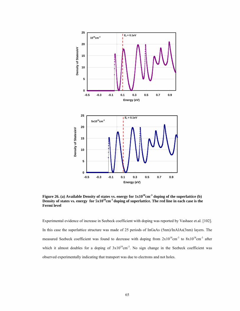
0
5
10
15
20
25
-0.5 -0.3 -0.1 0.1 0.3 0.5 0.7 0.9Energy (eV)
Den
sity
of S
tate
s/eV
Ef = 0.1eV1018cm-3
0
5
10
15
20
25
-0.5 -0.3 -0.1 0.1 0.3 0.5 0.7 0.9Energy (eV)
Den
sity
of S
tate
s/eV
Ef = 0.1eV5x1019cm-3
Figure 26. (a) Available Density of states vs. energy for 1x1018cm-3 doping of the superlattice (b) Density of states vs. energy for 5x1018cm-3 doping of superlattice. The red line in each case is the Fermi level
Experimental evidence of increase in Seebeck coefficient with doping was reported by Vashaee et.al. [102].
In this case the superlattice structure was made of 25 periods of InGaAs (5nm)/InAlAs(3nm) layers. The
measured Seebeck coefficient was found to decrease with doping from 2x1018cm-3 to 8x1018cm-3 after
which it almost doubles for a doping of 3x1019cm-3. No sign change in the Seebeck coefficient was
observed experimentally indicating that transport was due to electrons and not holes.
65
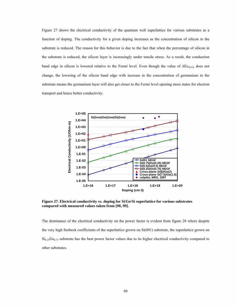
Figure 27 shows the electrical conductivity of the quantum well superlattice for various substrates as a
function of doping. The conductivity for a given doping increases as the concentration of silicon in the
substrate is reduced. The reason for this behavior is due to the fact that when the percentage of silicon in
the substrate is reduced, the silicon layer is increasingly under tensile stress. As a result, the conduction
band edge in silicon is lowered relative to the Fermi level. Even though the value of ∆EcSi-Ge does not
change, the lowering of the silicon band edge with increase in the concentration of germanium in the
substrate means the germanium layer will also get closer to the Fermi level opening more states for electron
transport and hence better conductivity.
1.E-05
1.E-04
1.E-03
1.E-02
1.E-01
1.E+00
1.E+01
1.E+02
1.E+03
1.E+04
1.E+05
1.E+16 1.E+17 1.E+18 1.E+19 1.E+20Doping (cm-3)
Elec
tric
al C
ondu
ctiv
ity (1
/Ohm
-m)
Si001 NEGFSi(0.75)Ge(0.25) NEGFSi(0.5)Ge(0.5) NEGFSi(0.25)Ge(0.75) NEGFCross-plane Si(8)/Ge(2)Cross-plane Si(7.5)/Ge(1.5)colpitts, MRS, 1997
Si(2nm)/Ge(2nm)/Si(2nm)
Figure 27. Electrical conductivity vs. doping for Si/Ge/Si superlattice for various substrates compared with measured values taken from [98, 99].
The dominance of the electrical conductivity on the power factor is evident from figure 28 where despite
the very high Seebeck coefficients of the superlattice grown on Si(001) substrate, the superlattice grown on
Si0.25Ge0.75 substrate has the best power factor values due to its higher electrical conductivity compared to
other substrates.
66
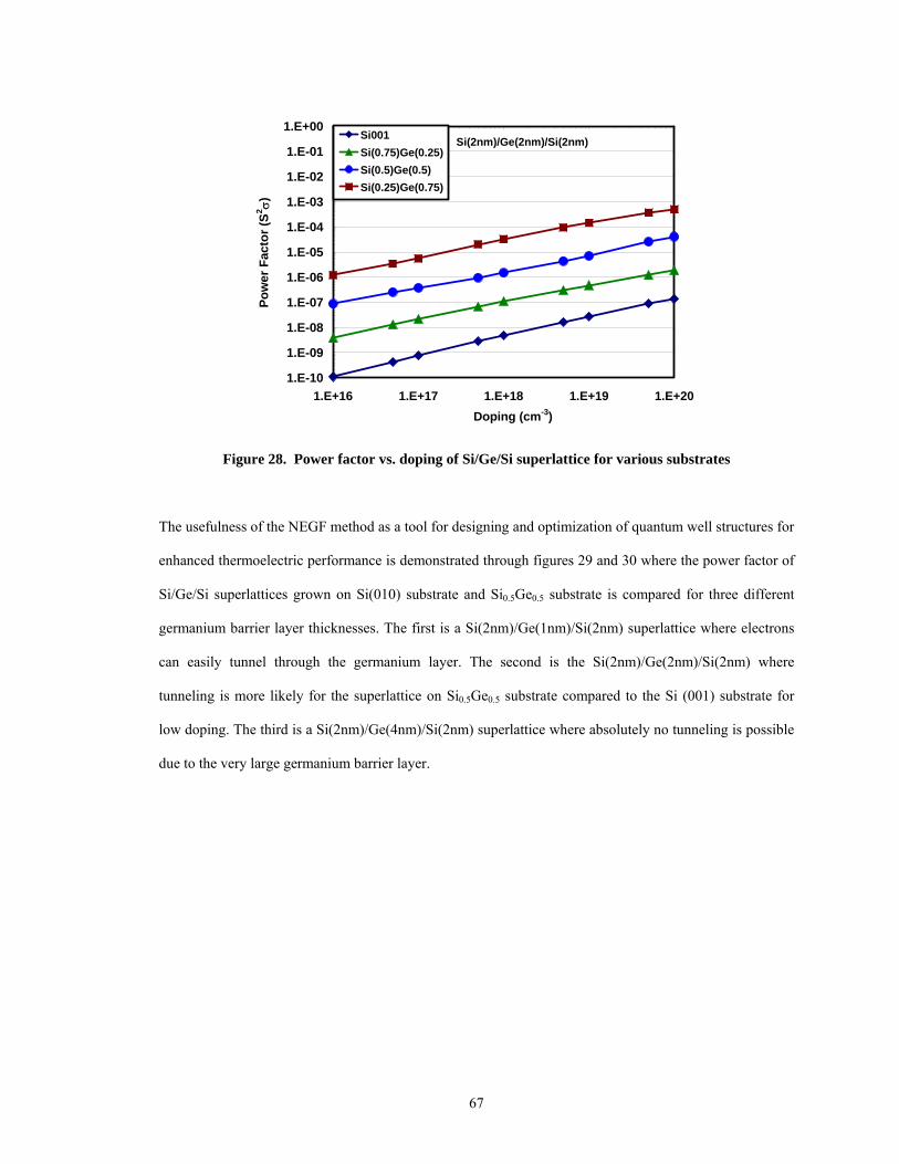
1.E-10
1.E-09
1.E-08
1.E-07
1.E-06
1.E-05
1.E-04
1.E-03
1.E-02
1.E-01
1.E+00
1.E+16 1.E+17 1.E+18 1.E+19 1.E+20Doping (cm-3)
Pow
er F
acto
r (S2 σ
)
Si001Si(0.75)Ge(0.25)Si(0.5)Ge(0.5)Si(0.25)Ge(0.75)
Si(2nm)/Ge(2nm)/Si(2nm)
Figure 28. Power factor vs. doping of Si/Ge/Si superlattice for various substrates
The usefulness of the NEGF method as a tool for designing and optimization of quantum well structures for
enhanced thermoelectric performance is demonstrated through figures 29 and 30 where the power factor of
Si/Ge/Si superlattices grown on Si(010) substrate and Si0.5Ge0.5 substrate is compared for three different
germanium barrier layer thicknesses. The first is a Si(2nm)/Ge(1nm)/Si(2nm) superlattice where electrons
can easily tunnel through the germanium layer. The second is the Si(2nm)/Ge(2nm)/Si(2nm) where
tunneling is more likely for the superlattice on Si0.5Ge0.5 substrate compared to the Si (001) substrate for
low doping. The third is a Si(2nm)/Ge(4nm)/Si(2nm) superlattice where absolutely no tunneling is possible
due to the very large germanium barrier layer.
67
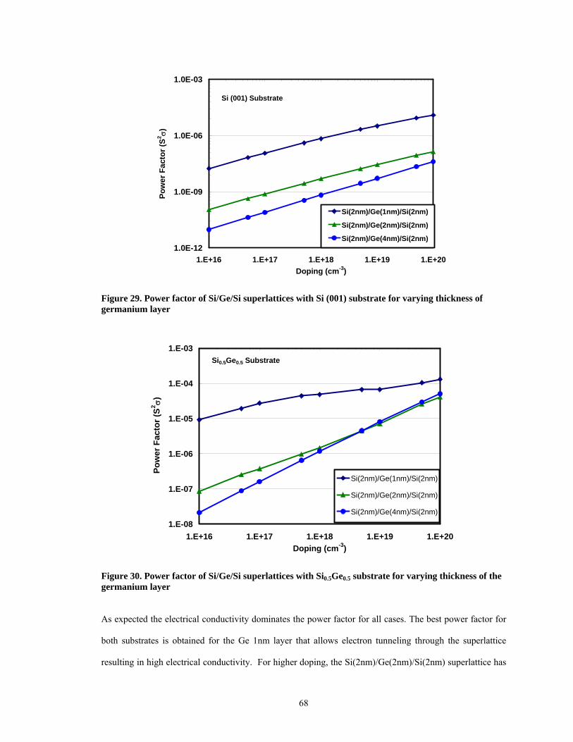
1.0E-12
1.0E-09
1.0E-06
1.0E-03
1.E+16 1.E+17 1.E+18 1.E+19 1.E+20Doping (cm-3)
Pow
er F
acto
r (S2 σ)
Si(2nm)/Ge(1nm)/Si(2nm)
Si(2nm)/Ge(2nm)/Si(2nm)
Si(2nm)/Ge(4nm)/Si(2nm)
Si (001) Substrate
Figure 29. Power factor of Si/Ge/Si superlattices with Si (001) substrate for varying thickness of germanium layer
1.E-08
1.E-07
1.E-06
1.E-05
1.E-04
1.E-03
1.E+16 1.E+17 1.E+18 1.E+19 1.E+20Doping (cm-3)
Pow
er F
acto
r (S2 σ)
Si(2nm)/Ge(1nm)/Si(2nm)
Si(2nm)/Ge(2nm)/Si(2nm)
Si(2nm)/Ge(4nm)/Si(2nm)
Si0.5Ge0.5 Substrate
Figure 30. Power factor of Si/Ge/Si superlattices with Si0.5Ge0.5 substrate for varying thickness of the germanium layer
As expected the electrical conductivity dominates the power factor for all cases. The best power factor for
both substrates is obtained for the Ge 1nm layer that allows electron tunneling through the superlattice
resulting in high electrical conductivity. For higher doping, the Si(2nm)/Ge(2nm)/Si(2nm) superlattice has
68
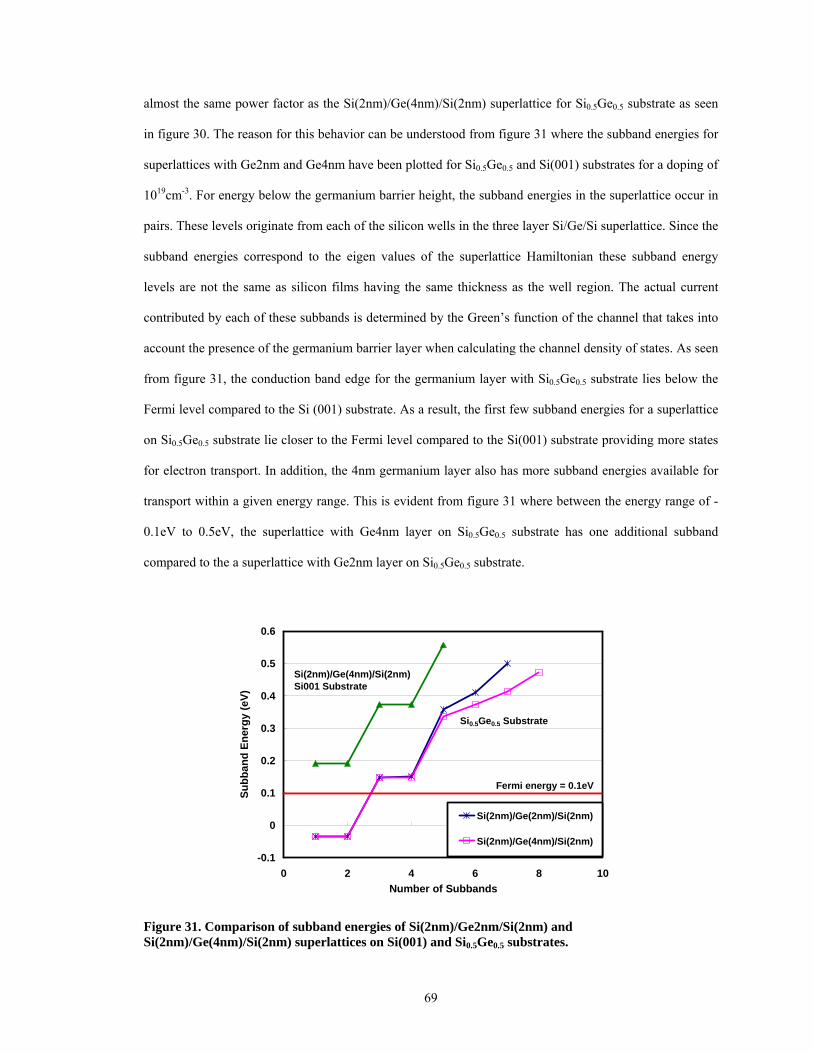
almost the same power factor as the Si(2nm)/Ge(4nm)/Si(2nm) superlattice for Si0.5Ge0.5 substrate as seen
in figure 30. The reason for this behavior can be understood from figure 31 where the subband energies for
superlattices with Ge2nm and Ge4nm have been plotted for Si0.5Ge0.5 and Si(001) substrates for a doping of
1019cm-3. For energy below the germanium barrier height, the subband energies in the superlattice occur in
pairs. These levels originate from each of the silicon wells in the three layer Si/Ge/Si superlattice. Since the
subband energies correspond to the eigen values of the superlattice Hamiltonian these subband energy
levels are not the same as silicon films having the same thickness as the well region. The actual current
contributed by each of these subbands is determined by the Green’s function of the channel that takes into
account the presence of the germanium barrier layer when calculating the channel density of states. As seen
from figure 31, the conduction band edge for the germanium layer with Si0.5Ge0.5 substrate lies below the
Fermi level compared to the Si (001) substrate. As a result, the first few subband energies for a superlattice
on Si0.5Ge0.5 substrate lie closer to the Fermi level compared to the Si(001) substrate providing more states
for electron transport. In addition, the 4nm germanium layer also has more subband energies available for
transport within a given energy range. This is evident from figure 31 where between the energy range of -
0.1eV to 0.5eV, the superlattice with Ge4nm layer on Si0.5Ge0.5 substrate has one additional subband
compared to the a superlattice with Ge2nm layer on Si0.5Ge0.5 substrate.
-0.1
0
0.1
0.2
0.3
0.4
0.5
0.6
0 2 4 6 8 10Number of Subbands
Subb
and
Ener
gy (e
V)
Si(2nm)/Ge(2nm)/Si(2nm)
Si(2nm)/Ge(4nm)/Si(2nm)
Si(2nm)/Ge(4nm)/Si(2nm)Si001 Substrate
Si0.5Ge0.5 Substrate
Fermi energy = 0.1eV
Figure 31. Comparison of subband energies of Si(2nm)/Ge2nm/Si(2nm) and Si(2nm)/Ge(4nm)/Si(2nm) superlattices on Si(001) and Si0.5Ge0.5 substrates.
69
The similar thermoelectric performance of the higher doped Ge2nm and Ge4nm superlattices on SixGe1-x
substrates can be taken advantage of during the fabrication of superlattices where interlayer diffusion
between very thin layers can be avoided by using a thicker germanium layer to obtain the desired
thermoelectric performance.
Effect of Electron-Phonon Scattering on the Power Factor of Si/Ge/Si Superlattices
Electron-optical phonon scattering was included in the NEGF to study the impact of scattering on the
thermoelectric performance of strained superlattices shown in figure 32. The study was done for the two
cases of Si(2nm)/Ge(1nm)/Si(2nm) superlattice on Si(001) and Si0.5Ge0.5 substrates since the superlattice
with this thickness had produced the highest power factor distribution with doping of all the structures
considered. Electron-phonon scattering caused the power factor of both superlattices to decrease due to
decrease in the electrical conductivity. Since the subband energies of the superlattice on Si0.5Ge0.5 substrate
lie closer to the Fermi level compared to the Si(001) substrate, the superlattice on Si0.5Ge0.5 substrate show
greater decrease in the current with scattering. As a result, the average decrease in the power factor for the
superlattice on Si0.5Ge0.5 substrate was 64% compared to the 43% decrease in the case of a Si(001)
substrate. However, the overall power factor of the superlattices on Si0.5Ge0.5 substrate with scattering was
still an order of magnitude greater than superlattices on the Si(001) substrate. The oscillations in the
Seebeck coefficient in the case of the Si0.5Ge0.5 substrate were also present in the power factor distribution
with doping. While increased doping is commonly associated with better conductivity and performance, the
Seebeck oscillations point to an interesting result where the power factor for 5x1018cm-3 doped superlattices
is lower than the power factor of the lesser doped 1x1018cm-3 superlattices.
70
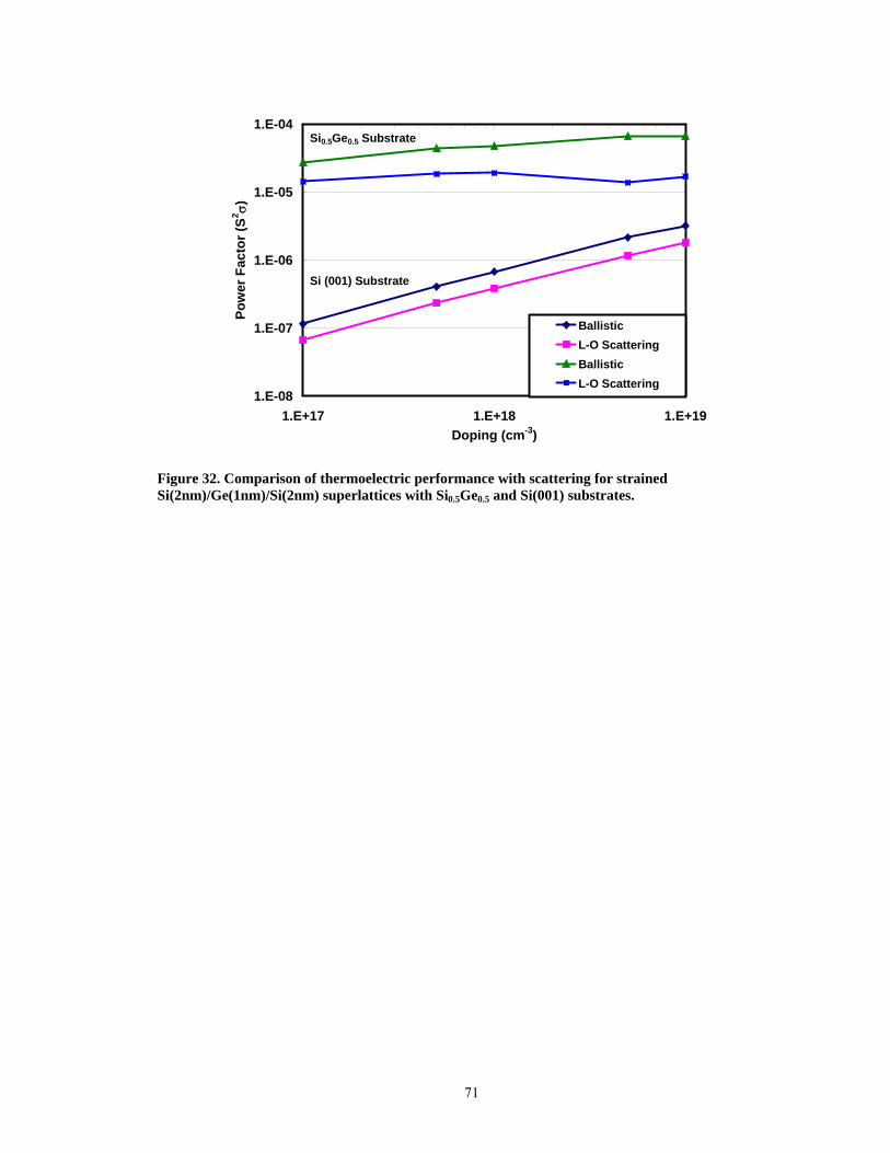
1.E-08
1.E-07
1.E-06
1.E-05
1.E-04
1.E+17 1.E+18 1.E+19Doping (cm-3)
Pow
er F
acto
r (S2 σ)
BallisticL-O ScatteringBallisticL-O Scattering
Si (001) Substrate
Si0.5Ge0.5 Substrate
Figure 32. Comparison of thermoelectric performance with scattering for strained Si(2nm)/Ge(1nm)/Si(2nm) superlattices with Si0.5Ge0.5 and Si(001) substrates.
71
CHAPTER VII
CONCLUSIONS
Reliance on Boltzmann-based models has produced a culture of “smaller is better” research, where the
reduction in size is expected to produce limitless increase in performance. Experimental observations
especially in the case of thermoelectric performance of nanoscale devices have not exhibited this behavior.
The motivation for this research stemmed out of a need to understand the disparity in theoretical
predictions and experimental observations.
Transport models based on Boltzmann and Fermi-Dirac statistics coupled in semi-classical transport have
been very effective in identifying the pertinent physical parameters responsible for thermoelectric
performance in bulk materials. The inclusion of various scattering mechanisms through the relaxation time
approach allow us to isolate and understand carrier scattering mechanisms that dominate thermoelectric
performance for a particular temperature range. While the semi-classical models work well in predicting
the performance of materials in the bulk regime, wave effects that cannot be captured naturally in particle-
based models begin to dominate in nanostructured materials. Reduced dimensionality results in phonon
confinement and formation of phonon bandgaps as well as tunneling and diffraction of electrons that are
characteristic of wave behavior. Furthermore, alteration of the dispersion relations of electrons and phonons
at nanoscales affects the way these carriers interact with each other. Figure 10 demonstrates that at length
scales near the room temperature de Broglie wavelength of electrons, phonons do not affect electron
transport significantly. This means that in devices at these length scales, carrier distribution is no longer in
equilibrium. Another important effect seen from figure 10 is the effect of electron confinement. Decreased
length scales lead to energy discretization limiting the number of energy states available to transport
electrons at the nanoscale leading to a decrease in current with shrinking device size for a constant field.
72
For materials at reduced scales, the governing physics changes enough that new models are required. A
quantum transport model that can successfully couple wave effects and scattering effects to predict
thermoelectric performance is introduced through the non-equilibrium Green's function method. Using an
effective mass Hamiltonian, current flow from the contacts is modeled as a modification of the channel
density of states through self energy terms in the Hamiltonian. In addition, the NEGF method does not
require a statistical distribution of carriers. This allows for the modeling of highly non-equilibrium
transport as well as the inclusion of rigorous scattering. The ability of the NEGF method to model quantum
effects purely based on first principles is evident from figure 20 where the conductivity predictions of the
NEGF and the semi-classical CRTA model are compared. While the NEGF model does not rely on any
external parameters other than the electron effective mass, the reliance of the CRTA model on external
electron mobility data for conductivity predictions demonstrates the empirical nature of the semi-classical
Boltzmann model. In addition to successfully coupling quantum and scattering effects, the NEGF method
allows us to seamlessly include various parameters that affect thermoelectric performance such as
bandgaps, doping, and effective mass.
The NEGF method is used to study the effect of electron confinement on silicon nanofilms and wires.
Electron confinement results in almost a factor of 4 decrease in the electrical conductivity of the 6nm
silicon film compared to the 12nm film. Increase in the amount of confinement also leads to a 33%
decrease in the conductivity of a 6nm x 6nm wire compared to the 6nm film. Electron-optical phonon
scattering was included in the NEGF using the concept of Buttiker probes where scattering is treated as
another contact. Scattering with optical phonons was found to have a greater effect on the 12nm film where
the current decreased by 45% of its ballistic value.
Thermoelectric performance of quantum well superlattices is studied using the NEGF model with the
inclusion of substrate strain and optical phonon scattering. The power factor of a single period superlattice
is compared for various substrates. It was found that a substrate rich in germanium would lower the energy
of the conduction band valley in silicon to providing more states around the Fermi energy for electron
transport. Such substrates also produce oscillations in the Seebeck coefficient that are attributed to the shift
73
in subband energies around the conduction band due to doping. These effects cannot be captured in semi-
classical models without introducing some form of quantum corrections.
The power factor of the superlattices was found to be dominated by the electrical conductivity despite the
very high Seebeck coefficients of the Si(001) substrates that were poor electrical conductors. The
thermoelectric performance of superlattices was also studied as a function of the germanium barrier
thickness. Overall, despite a 64% decrease in conductivity due to electron-phonon scattering, the best
thermoelectric performance was obtained for superlattices with germanium rich substrates having barriers
that allowed tunneling as in the case of a Si(2nm)/Ge(1nm)/Si(2nm) structure on Si0.5Ge0.5 substrate. The
Seebeck oscillations produced by germanium rich substrates could be exploited to design structures with
high power factors for low doping. The coupled thermoelectric solution combined with quantum and
scattering effects in superlattices demonstrates the capability of the NEGF method as a platform to design
structures with enhanced figure of merit.
The NEGF model suggests that optimization of devices is possible. Although this places theoretical upper
limits on performance, there is no indication that these theoretical limits have been reached and continued
research is warranted. While quantum effects are inherent in the NEGF model, the effect of various
scattering mechanisms such as electron-impurity scattering and intersubband electron-phonon scattering
must be further explored to fully gauge the performance of nanoscale structures. This research started as an
attempt to explain the discrepancy between theoretical predictions and experimental data of nanoscale
devices. Not only have we identified the pertinent physics that explain the discrepancy, but we have also
developed a framework for further studies on performance of highly scaled thermoelectric devices. Now
device designers have a tool with appropriate predictive power to guide the continued search for high
efficiency materials.
74
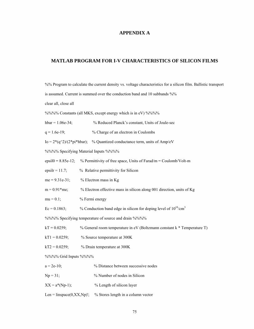
APPENDIX A
MATLAB PROGRAM FOR I-V CHARACTERISTICS OF SILICON FILMS
%% Program to calculate the current density vs. voltage characteristics for a silicon film. Ballistic transport
is assumed. Current is summed over the conduction band and 10 subbands %%
clear all, close all
%%%% Constants (all MKS, except energy which is in eV) %%%%
hbar = 1.06e-34; % Reduced Planck’s constant, Units of Joule-sec
q = 1.6e-19; % Charge of an electron in Coulombs
Io = 2*(q^2)/(2*pi*hbar); % Quantized conductance term, units of Amp/eV
%%%% Specifying Material Inputs %%%%
epsil0 = 8.85e-12; % Permittivity of free space, Units of Farad/m = Coulomb/Volt-m
epsilr = 11.7; % Relative permittivity for Silicon
me = 9.31e-31; % Electron mass in Kg
m = 0.91*me; % Electron effective mass in silicon along 001 direction, units of Kg
mu = 0.1; % Fermi energy
Ec = 0.1863; % Conduction band edge in silicon for doping level of 1018/cm3
%%%% Specifying temperature of source and drain %%%%
kT = 0.0259; % General room temperature in eV (Boltzmann constant k * Temperature T)
kT1 = 0.0259; % Source temperature at 300K
kT2 = 0.0259; % Drain temperature at 300K
%%%% Grid Inputs %%%%
a = 2e-10; % Distance between successive nodes
Np = 31; % Number of nodes in Silicon
XX = a*(Np-1); % Length of silicon layer
Len = linspace(0,XX,Np)'; % Stores length in a column vector
75
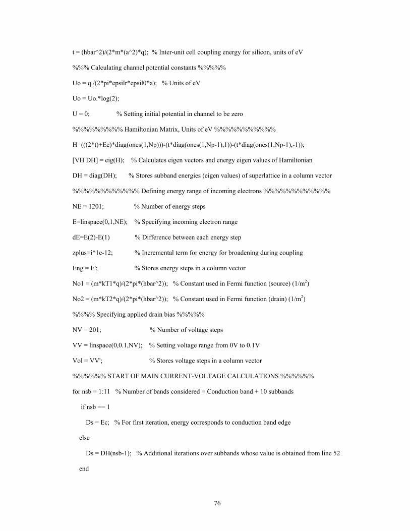
t = (hbar^2)/(2*m*(a^2)*q); % Inter-unit cell coupling energy for silicon, units of eV
%%% Calculating channel potential constants %%%%%
Uo = q./(2*pi*epsilr*epsil0*a); % Units of eV
Uo = Uo.*log(2);
U = 0; % Setting initial potential in channel to be zero
%%%%%%%%% Hamiltonian Matrix, Units of eV %%%%%%%%%%%
H=(((2*t)+Ec)*diag(ones(1,Np)))-(t*diag(ones(1,Np-1),1))-(t*diag(ones(1,Np-1),-1));
[VH DH] = eig(H); % Calculates eigen vectors and energy eigen values of Hamiltonian
DH = diag(DH); % Stores subband energies (eigen values) of superlattice in a column vector
%%%%%%%%%%%% Defining energy range of incoming electrons %%%%%%%%%%%%
NE = 1201; % Number of energy steps
E=linspace(0,1,NE); % Specifying incoming electron range
dE=E(2)-E(1) % Difference between each energy step
zplus=i*1e-12; % Incremental term for energy for broadening during coupling
Eng = E'; % Stores energy steps in a column vector
No1 = (m*kT1*q)/(2*pi*(hbar^2)); % Constant used in Fermi function (source) (1/m2)
No2 = (m*kT2*q)/(2*pi*(hbar^2)); % Constant used in Fermi function (drain) (1/m2)
%%%% Specifying applied drain bias %%%%%
NV = 201; % Number of voltage steps
VV = linspace(0,0.1,NV); % Setting voltage range from 0V to 0.1V
Vol = VV'; % Stores voltage steps in a column vector
%%%%%% START OF MAIN CURRENT-VOLTAGE CALCULATIONS %%%%%%
for nsb = 1:11 % Number of bands considered = Conduction band + 10 subbands
if nsb == 1
Ds = Ec; % For first iteration, energy corresponds to conduction band edge
else
Ds = DH(nsb-1); % Additional iterations over subbands whose value is obtained from line 52
end
76
No = 0; % For each subband, setting initial electron density in channel to be zero
Sig1 = zeros(Np,Np); Sig2 = zeros(Np,Np); % Initial values for self energy matrices
%%%%%%%%%%%%%%%%%%%%%%%%%%%%%%%%%%%%%%%%%%
for b = 1:NV % Start of voltage loop
V = VV(b); % Voltage input for each step
chg = 1; % Initial guess for potential change
while chg > 1e-6 % Checks potential change
Rh = 0; % Initial electron density along length of channel
for k = 1:NE % Starting energy loop for incoming electron energy
%%% Calculating Fermi functions of electrons entering through Silicon Source and Drain
%%%
f1 = No1*log(1+exp((-(E(k)-mu))/kT1)); % 2D source Fermi function. Units of 1/m2
f2 = No2*log(1+exp((-(E(k)-mu + V))/kT2)); % 2D drain Fermi function. Units of 1/m2
%%%%%%%%%%%%%%%%%%%%%%%%%%%%%%%%%%%%%%%%%%
ka1 = acos(1 - ((E(k) + zplus - Ds)/(2*t ))); % Wave vector of broadened waves at source
Sig1(1,1) = -t*exp(i*ka1); % Self energy of source (eV)
Gam1 = i*(Sig1 - Sig1'); % Source broadening matrix (eV)
SigIn1 = Gam1*f1; % Inscattering term for source (eV)
ka2 = acos(1 - ((E(k) + zplus - Ds + V)/(2*t))); % Wave vector of broadened waves at drain
Sig2(Np,Np) = -t*exp(i*ka2); % Self energy of drain (eV)
Gam2 = i*(Sig2 - Sig2'); % Drain broadening matrix (eV)
SigIn2 = Gam2*f2; % Inscattering term for drain (eV)
G = inv(((E(k) + zplus)*eye(Np)) -H -diag(U) -Sig1 -Sig2); % Green's function (1/eV)
A = i*(G - G'); % Channel density of states matrix (1/eV)
Gn = G*(SigIn1+SigIn2)*G'; % Electron density matrix in channel (1/eV-m2)
77
Rh = Rh + (dE/(2*pi))*Gn; % Calculating electron density in the channel (1/m2)
T = Gam1*G*Gam2*G'; % Transmission function (no units, number)
IT(k) = real(trace(T*(f1-f2))); % Transmission current for each energy step (number/m2)
I1(k) = real(trace(SigIn1*A) - trace(Gam1*Gn)); % Source current for each energy step
(Number/m2)
I2(k) = -real(trace(SigIn2*A) - trace(Gam2*Gn)); % Drain current for each energy step
(Number/m2)
end % End of energy loop
%%%%%%%%%% Self consistent potential calculation %%%%%%%%%
N = real(diag(Rh)); % Stores diagonal elements (along length of channel) of density matrix,
Units of 1/m2
Unew = Uo.*(N-No)*(a^2); % Calculates new channel potential from change in electron density
(eV)
dU = Unew-U; % Change in channel potential due to new electron density
chg = max(abs(dU))
U = U + 0.2*dU; % Updating channel potential with respect to old potential
if V == 0
No = N;, chg = 0;
end
Rho = N/a; % Normalized electron density per unit cell (1/m3)
end % End of potential while loop each voltage step
Den(:,b) = Rho; % Stores electron density in channel for each voltage for the present subband
Pot(:,b) = U; % Stores potential in channel for each voltage for the present subband
IE1(:,b) = I1’; % Current density per unit energy at source for each voltage
IE2(:,b) = I2’; % Current density per unit energy at drain for each voltage
Is(b) = dE*Io*sum(I1); % Net source current density summed over all energies for each voltage step
Isc = Is’;
78
Id(b) = dE*Io*sum(I2); % Net drain current density summed over all energies for each voltage step
Idr = Id’;
I(b) = dE*Io*sum(IT); % Net transmission current summed over all energies for each voltage step
Itr = I’
end % End of each voltage step loop
Isb(:,nsb) = Itr; % Transmission current for each subband
Isbs(:,nsb) = Isc; % Source current for each subband
Isbd(:,nsb) = Idr; % Drain current for each subband
end % End of subband loop
II = sum(Isb,2) % Sum of current from all subbands for each voltage step
hold on
dlmwrite(‘Len.dat’,Len,’,’); % Stores length of the channel
dlmwrite(‘Vol.dat’,Vol,’,’); % Stores applied voltage range with incremental steps
dlmwrite(‘Eng.dat’,Eng,’,’); % Stores electron energy range with incremental steps
dlmwrite(‘Isb.dat’,Isb,’\t’); % Stores transmission current for each subband for each voltage step
dlmwrite(‘Isbs.dat’,Isbs,’\t’); % Stores source current for each subband for each voltage step
dlmwrite(‘Isbd.dat’,Isbd,’\t’); % Stores drain current for each subband for each voltage step
dlmwrite(‘II.dat’,II,’,’); % Stores sum of currents from all subbands for each voltage step
79
APPENDIX B
MATLAB PROGRAM FOR I-V CHARACTERISTICS OF SILICON WIRES
%% Program to calculate current density vs. voltage characteristics for a silicon wire. Confined dimensions
are along the Lx and Ly directions. The Lz direction has infinite length. Ballistic transport along Lx is
assumed. The calculated current is summed over the conduction band and 10 subbands.
clear all, close all
%%%%% Constants (all MKS, except energy which is in eV) %%%%%
hbar=1.06e-34; % Reduced Planck’s constant, Units of Joule-sec
q = 1.6e-19; % Charge of an electron in Coulombs
Io = 2*(q^2)/(2*pi*hbar); % Quantized conductance term, units of Amp/eV
%%%%%%%%% Specifying Material Inputs %%%%%%%%%%%
epsil0 = 8.85e-12; % Permittivity of free space, Units of Farad/m = Coulomb/Volt-m
epsilr = 11.7; % Relative permittivity for Silicon
me = 9.31e-31; % Electron mass in Kg
m = 0.91*me; % Electron effective mass in silicon along 001 direction, units of Kg
mu = 0.1; % Fermi energy
Ec = 0.1863; % Conduction band edge in silicon for doping level of 1018/cm3
%%%%%%% Specifying temperature of source and drain %%%%%%%%
kT = 0.0259; % General room temperature in eV (Boltzmann constant k * Temperature T)
kT1 = 0.0259; % Source temperature at 300K
kT2 = 0.0259; % Drain temperature at 300K
%%%%%%%%%%% Grid Inputs %%%%%%%%%%%%
a = 3e-10; % Distance between successive nodes
Nx = 21; % Number of nodes in Silicon along the Lx direction
Ny = 21; % Number of nodes in Silicon along the Ly direction
80
Np = Nx*Ny; % Total number of nodes for the square grid
XX = a*(Nx-1); % Length of Lx direction
YY = a*(Ny-1); % Length of Ly direction
Lx = linspace(0,XX,Nx)'; % Stores length in a column vector
Ly = linspace(0,YY,Ny)'; % Stores length in a column vector
%%%%%%%%%%%%%%%%%%%%%%%%%%%%%%%%%%%%%%
t = (hbar^2)/(2*m*(a^2)*q); % Inter-unit cell coupling energy for silicon, units of eV
%%%%%%%%% Calculating channel potential constants %%%%%%%%%%%%
Uo = q./(2*pi*epsilr*epsil0*a); % Units of eV
Uo = Uo.*log(2);
U = 0; % Setting initial potential in channel to be zero
%%%%%%%%%%%% Hamiltonian Matrix, Units of eV %%%%% %%%%
H = zeros(Np,Np);
for n = 1:Np
H(n,n) = Ec + 4*t; %% Specifies main diagonal terms
end
j = 1;
for r = 1:Ny; %% For each row of nodes along Ly
for n = 1:(Nx-1) %% Specifies x-axis off-diagonal terms for each node along Lx
H(j,j+1) = -t;
H(j+1,j) = -t;
j = j+1;
end
j = j+1; %% Jumps to the next row of nodes along Ly
end
j = Nx+1; %% For each node point counting from 1 along Lx
for r = 1:(Np-Nx) %% Specifies Y-axis off-diagonal terms
H(r,j) = -t;
81
H(j,r) = -t;
j = j+1;
end
%%%%%%%%%%%%%%%%%%%%%%%%%%%%%%%%%%%%%%%
[VH DH] = eig(H); % Calculates eigen vectors and energy eigen values of Hamiltonian
DH = diag(DH); % Stores subband energies (eigen values) of superlattice in a column vector
%%%%%%%%%%% Defining energy range of incoming electrons %%%%%%%%%%%%
NE = 601; % Number of energy steps
E=linspace(0,1,NE); % Specifying incoming electron range
dE=E(2)-E(1) % Difference between each energy step
zplus=i*1e-12; % Incremental term for energy for broadening during coupling
Eng = E'; % Stores energy steps in a column vector
N1 = ((hbar^2)/(2*m*kT1*q)); % Constant used in Fermi function (source) Units of (m^2)
C1 = (1/(4*pi))*sqrt(1/N1); % Constant used in Fermi function (source) Units of 1/m
N2 = ((hbar^2)/(2*m*kT2*q)); % Constant used in Fermi function (drain) Units of (m^2)
C2 = (1/(4*pi))*sqrt(1/N2); % Constant used in Fermi function (drain) Units of 1/m
%%%%%%%%%%% Specifying applied drain bias %%%%%%%%%%%%
NV = 31; % Number of voltage steps
VV = linspace(0,0.03,NV); % Setting voltage range from 0V to 0.03V
Vol = VV'; % Stores voltage steps in a column vector
%%%%%%%%%%% START OF MAIN CURRENT-VOLTAGE CALCULATIONS %%%% %%%%%
for nsb = 1:11 % Number of bands considered = Conduction band + 10 subbands
if nsb == 1
Ds = Ec; % For first iteration, energy corresponds to conduction band edge
else
Ds = DH(nsb-1); % Additional iterations over subbands whose value is obtained from line 52
end
82
No = 0; % For each subband, setting initial electron density in channel to be zero
Sig1 = zeros(Np,Np); Sig2 = zeros(Np,Np); % Initial values for self energy matrices
for b = 1:NV % Start of voltage loop
V = VV(b); % Voltage input for each step
chg = 1; % Initial guess for potential change
while chg > 1e-6 % Checks potential change
Rh = 0; % Initial electron density along length of channel
for k = 1:NE % Starting energy loop for incoming electron energy
% Calculating Fermi functions of electrons entering through Silicon Source and Drain %
x = -(E(k) - mu)/kT1;
X1(k) = x;
if x < 2
f1 = C1*Fermi1(x); % 1D Source Fermi function. Units of 1/m
else
f1 = C1*Fermi2(x); % 1D Source Fermi function. Units of 1/m
end
ferm1(k,b) = f1; % Stores fermi function values for each energy
x = -(E(k) - mu + V)/kT2;
X2(k) = x;
if x < 2
f2 = C2*Fermi1(x); % 1D Drain fermi function. Units of 1/m
else
f2 = C2*Fermi2(x); % 1D Drain fermi function. Units of 1/m
end
ferm2(k,b) = f2; % Stores fermi function values for each energy
%%%%%%%%%%%%%%%%%%%%%%%%%%%%%%%%%%%%%%%%%%%%%%%
ka1 = acos(1 - ((E(k) + zplus - Ec - Ds)/(2*t))); % Wave vector of broadened waves at source
j = 1;
83
for n = 1:Ny
Sig1(j,j) = -t*exp(i*ka1); % Self energy of source (eV)
j = j + Nx;
end
Gam1 = i*(Sig1 - Sig1'); % Source broadening matrix (eV)
ka2 = acos(1 - ((E(k) + zplus - Ec - Ds + V)/(2*t))); % Wave vector of broadened waves at source
j = Nx;
for n = 1:Ny
Sig2(j,j) = -t*exp(i*ka2); % Self energy of drain (eV)
j = j + Nx;
end
Gam2 = i*(Sig2 - Sig2'); % Drain broadening matrix (eV)
G = inv(((E(k) + zplus)*eye(Np)) -H -diag(U) -Sig1 -Sig2); % Green's function (1/eV)
A = i*(G - G'); % Channel density of states matrix (1/eV)
SigIn1 = Gam1*f1; % Inscattering term for source Units of eV/m
SigIn2 = Gam2*f2; % Inscattering term for drain Units of eV/m
SigIn = SigIn1 + SigIn2;
Gn = G*SigIn*G'; % Electron density matrix in channel (1/eV-m)
Rh = Rh + (dE/(2*pi))*(Gn); % Calculating electron density in the channel (1/m)
T = Gam1*G*Gam2*G'; % Transmission function (no units, number)
IT(k) = real(trace(T*(f1-f2))); % Transmission current for each energy step (number/m2)
I1(k) = real(trace(SigIn1*A) - trace(Gam1*Gn)); % Source current for each energy step
(Number/m)
84
I2(k) = -real(trace(SigIn2*A) - trace(Gam2*Gn)); % Drain current for each energy step
(Number/m)
end % End of energy loop
%%%%% Self consistent potential calculation %%%%%
N = real(diag(Rh)); % Stores diagonal elements (along length of channel) of density matrix
(1/m)
Unew = Uo.*(N-No)*a; % Channel potential (eV)
dU = Unew-U; % Change in channel potential due to new electron density
chg = max(abs(dU))
U = U + 0.2*dU; % Updating channel potential with respect to old potential
if V ==0
No = N; chg = 0;
end
Rho = N/(a*a); % Normalized electron density per unit cell (1/m3)
end % End of potential while loop
Den(:,b) = Rho; % Stores electron density in channel for each voltage for the present subband
Pot(:,b) = U; % Stores potential in channel for each voltage for the present subband
IE1(:,b) = I1'; % Current density per unit energy at source for each voltage
IE2(:,b) = I2'; % Current density per unit energy at drain for each voltage
Is(b) = dE*Io*sum(I1); % Net source current density summed over all energies for each voltage step
Isc = Is';
Id(b) = dE*Io*sum(I2); % Net drain current density summed over all energies for each voltage step
Idr = Id';
I(b) = dE*Io*sum(IT); % Net transmission current summed over all energies for each voltage step
Itr = I'
end % End of each voltage step loop
Isb(:,nsb) = Itr; % Transmission current for each subband
85
Isbs(:,nsb) = Isc; % Source current for each subband
Isbd(:,nsb) = Idr; % Drain current for each subband
end %%% End of subband loop
II = sum(Isb,2) % Sum of current from all subbands for each voltage step
hold on
dlmwrite('Len.dat',Len,','); % Stores length of the channel
dlmwrite('Vol.dat',Vol,','); % Stores applied voltage range with incremental steps
dlmwrite('Eng.dat',Eng,','); % Stores electron energy range with incremental steps
dlmwrite('Isb.dat',Isb,'\t'); % Stores transmission current for each subband for each voltage step
dlmwrite('Isbs.dat',Isbs,'\t'); % Stores source current for each subband for each voltage step
dlmwrite('Isbd.dat',Isbd,'\t'); % Stores drain current for each subband for each voltage step
dlmwrite('II.dat',II,','); % Stores sum of currents from all subbands for each voltage step
86
APPENDIX C
MATLAB PROGRAM FOR I-V CHARACTERISTICS OF STRAINED SI/GE/SI SUPERLATTICES
%%% Program to calculate current density vs. voltage characteristics for a strained Si/Ge/Si superlattice.
Ballistic transport is assumed. Current is summed over conduction band and 10 subbands. %%%
clear all, close all
%%%%% Constants (all MKS, except energy which is in eV) %%%%%
hbar=1.06e-34; % Reduced Plancks constant, Units of Joule-sec
q = 1.6e-19; % Charge of an electron in Coulombs
Io = 2*(q^2)/(2*pi*hbar); % Quantized conductance term, units of Amp/eV
%% Specifying Material Inputs %%
epsil0 = 8.85e-12; % Permittivity of free space, Units of Farad/m = Coulomb/Volt-m
epsilrS = 11.7; % Relative permittivity for Silicon
epsilrG = 16; % Relative permittivity for Germanium
epsilrJ = 0.5*(epsilrS + epsilrG); % Relative permittivity of the Si/Ge junction
me = 9.31e-31; % Electron mass in Kg
ms = 0.91*me; % Silicon effective mass along 001 direction
mg = 0.95*me; % Germanium effective mass along 001 direction
mu = 0.1; % Fermi energy
Ecs = 0.1863; % Conduction band edge in silicon for doping level of 1018/cm3
Ecg = 0.1606; % Conduction band edge in germanium for doping level of 1018/cm3
%%%%%%% Input Parameters to Calculate Strain %%%%%%%
a0Si = 5.4307; % Silicon Lattice constant parallel to substrate
a0Ge = 5.6579; % Germanium Lattice constant parallel to substrate
D001Si = 0.7713; % Silicon deformation potential
D001Ge = 0.7509; % Germanium deformation potential
87
EdUSi = 9.16;
EdUGe = 9.42;
%%%%%%%% Calculation of substrate lattice constant %%%%%%%%%
% Concentration of silicon in Si(x)Ge(1-x) substrate
x = 1; % Si 001 substrate
% x = 0.5; % Si(0.5)Ge(0.5) substrate
a11 = x*(a0Si) + (1-x)*(a0Ge); % Lattice constant parallel to the superlattice layers
%%%%%%%%% Silicon Strain Parameters %%%%%%%%%%
a_1Si = a0Si*(1-D001Si*((a11/a0Si)-1)); % Lattice constant perpendicular to the layers
eps_parSi = (a11 - a0Si)/a0Si; % Strain parallel to the silicon layers
eps_perSi = (a_1Si - a0Si)/a0Si; % Strain perpendicular to the layers
dEcs = (2/3)*(EdUSi)*(eps_perSi - eps_parSi); % Shift in the conduction band edge due to strain
%% Germanium strain parameters %%
a_1Ge = a0Ge*(1-D001Ge*((a11/a0Ge)-1)); % Lattice constant perpendicular to the layers
eps_parGe = (a11 - a0Ge)/a0Ge; % Strain parallel to the silicon layers
eps_perGe = (a_1Ge - a0Ge)/a0Ge; % Strain perpendicular to the layers
dEcg = (2/3)*(EdUGe)*(eps_perGe - eps_parGe); % Shift in the conduction band edge due to strain
%%%%%%% New conduction band edges due to shift in band edges with strain %%%%%%%%
Ecs = Ecs + dEcs; % New conduction band edge in silicon
Ecg = Ecg + dEcg; % New conduction band edge in germanium
Ecb = 0.5*(Ecs + Ecg); % Conduction band at interface of Si and Ge
%%%%%%%% Specifying temperature of source and drain %%%%%%%
kT = 0.0259; % General room temperature in eV (Boltzmann constant k * Temperature T)
kT1 = 0.0259; % Source temperature at 300K
kT2 = 0.0259; % Drain temperature at 300K
%%%%%%%%% Grid Inputs %%%%%%%%%%
a = 2e-10; % Distance between successive nodes
Ns = 11; % Number of nodes in Silicon
88
Ng = 11; % Number of nodes in germanium
Ni = 2; % Number of Si-Ge interfaces
NC = Ns+Ng+Ns; % Total number of nodes for Si/Ge/Si
Np = (NC-Ni); % Actual number of nodes describing the superlattice
XS = a*(Ns-1); % Length of silicon layer
XG = a*(Ng-1); % Length of germanium layer
XX=a*(Np-1); % Total length of superlattice
Len = linspace(0,XX,Np)'; % Stores length in a column vector
%%%%%%%%%%%%%%%%%%%%%%%%%%%%%%%%%%%%%%%%%%%%%%
ts = (hbar^2)/(2*ms*(a^2)*q); % Inter-unit cell coupling energy for silicon
tg = (hbar^2)/(2*mg*(a^2)*q); % Inter-unit cell coupling energy for germanium
%%%%%%%%% Calculating the Superlattice Permittivity %%%%%%%%%%%
epsilr = zeros(Np,1); % Specifying size of permittivity matrix
n = 1;
for n = n:(n+Ns-2)
epsilr(n,1) = epsilrS; % Inputs silicon permittivity
end
n = n+1;
epsilr(n,1) = epsilrJ; % Inputs interface permittivity
n = n+1;
for n = n:(n+Ng-3)
epsilr(n,1) = epsilrG; % Inputs germanium permittivity
end
n = n+1;
epsilr(n,1) = epsilrJ; % Inputs interface permittivity
n = n+1;
for n = n:(n+Ns-2)
epsilr(n,1) = epsilrS; % Inputs silicon permittivity
89
end
%%%%%%% Calculating Channel Potential Constants %%%%%%%%
Uo = q./(2*pi*epsilr*epsil0*a); % Units of eV
Uo = Uo.*log(2);
U = 0; % Setting initial potential in channel to be zero
%%%%%%%%%% Hamiltonian Matrix, Units of eV %%%%%%%%
H = zeros(Np,Np);
n = 1;
for r = 1:1
for n = n:(n + Ns-2)
H(n,n) = Ecs + (2*ts);
end
n = n+1;
H(n,n) = Ecb + ts+tg;
n = n+1;
for n = n:(n + Ng-3)
H(n,n) = Ecg + (2*tg);
end
n = n+1;
H(n,n) = Ecb + ts+tg;
n = n+1;
for n = n:(n + Ns-2)
H(n,n) = Ecs + (2*ts);
end
end
%%%%%%%%% Specifying off-diagonal terms %%%%%%%%
n = 1;
for r = 1:1
90
for n = n:(n + Ns-2)
H(n,n+1) = -ts;
H(n+1,n) = -ts;
end
n = n+1;
for n = n:(n + Ng-2)
H(n,n+1) = -tg;
H(n+1,n) = -tg;
end
n = n+1;
for n = n:(n + Ns-2)
H(n,n+1) = -ts;
H(n+1,n) = -ts;
end
end
[VH DH] = eig(H); % Calculates eigen vectors and energy eigen values of Hamiltonian
DH = diag(DH); % Stores subband energies (eigen values) of superlattice in a column vector
%%%%%%%% Defining energy range of incoming electrons %%%%%%%%%%
NE = 1201; % Number of energy steps
E=linspace(0,1,NE); % Specifying incoming electron range
dE=E(2)-E(1) % Difference between each energy step
zplus=i*1e-12; % Incremental term for energy for broadening during coupling
Eng = E'; % Stores energy steps in a column vector
No1 = (ms*kT1*q)/(2*pi*(hbar^2)); % Constant used in Fermi function (source) (1/m2)
No2 = (ms*kT2*q)/(2*pi*(hbar^2)); % Constant used in Fermi function (drain) (1/m2)
%% Specifying applied drain bias %%
NV = 201; % Number of voltage steps
VV = linspace(0,0.1,NV); % Setting voltage range from 0V to 0.1V
91
Vol = VV'; % Stores voltage steps in a column vector
%%%%%%%%% START OF MAIN CURRENT-VOLTAGE CALCULATIONS %%%%%%%%%
for nsb = 1:11 % Number of bands considered = Conduction band + 10 subbands
if nsb == 1
Ds = Ecs; % For first iteration, energy corresponds to conduction band edge
else
Ds = DH(nsb-1); % Additional iterations over subbands whose value is obtained from line 143
end
No = 0; % For each subband, setting initial electron density in channel to be zero
Sig1 = zeros(Np,Np); Sig2 = zeros(Np,Np); % Initial values for self energy matrices
for b = 1:NV % Start of voltage loop
V = VV(b); % Voltage input for each step
chg = 1; % Initial guess for potential change
while chg > 1e-6 % Checks potential change
Rh = 0; % Initial electron density along length of channel
for k = 1:NE % Starting energy loop for incoming electron energy
%% Calculating Fermi functions of electrons entering through Silicon Source and Drain %%
f1 = No1*log(1+exp((-(E(k)-mu))/kT1)); % 2D Source fermi function. Units of 1/m2
f2 = No2*log(1+exp((-(E(k)-mu + V))/kT2)); % 2D drain fermi function. Units of 1/m2
ka1 = acos(1 - ((E(k) + zplus - Ds)/(2*ts))); % Wave vector of broadened waves at source
Sig1(1,1) = -ts*exp(i*ka1); % Self energy of source (eV)
Gam1 = i*(Sig1 - Sig1'); % Source broadening matrix (eV)
SigIn1 = Gam1*f1; % Inscattering term for source (eV)
ka2 = acos(1 - ((E(k) + zplus - Ds + V)/(2*ts))); % Wave vector of broadened waves at drain
Sig2(Np,Np) = -ts*exp(i*ka2); % Self energy of drain (eV)
Gam2 = i*(Sig2 - Sig2'); % Drain broadening matrix (eV)
92
SigIn2 = Gam2*f2; % Inscattering term for drain (eV)
G = inv(((E(k) + zplus)*eye(Np)) -H -diag(U) -Sig1 -Sig2); % Green's function (1/eV)
A = i*(G - G'); % Channel density of states matrix (1/eV)
Gn = G*(SigIn1+SigIn2)*G'; % Electron density matrix in channel (1/eV-m2)
Rh = Rh + (dE/(2*pi))*Gn; % Calculating electron density in the channel (1/m2)
T = Gam1*G*Gam2*G'; % Transmission function (no units, number)
IT(k) = real(trace(T*(f1-f2))); % Transmission current for each energy step (number/m2)
I1(k) = real(trace(SigIn1*A) - trace(Gam1*Gn)); % Source current for each energy step 1/m2
I2(k) = -real(trace(SigIn2*A) - trace(Gam2*Gn)); % Current for each energy step at drain 1/m2
end % End of energy loop
%%%%% Self consistent potential calculation %%%%%%
N = real(diag(Rh)); % Stores diagonal elements (along length of channel) of density matrix (1/m2)
Unew = Uo.*(N-No)*(a^2); % Channel potential (eV)
dU = Unew-U; % Change in channel potential due to new electron density
chg = max(abs(dU))
U = U + 0.2*dU; % Updating channel potential with respect to old potential
if V == 0
No = N; chg = 0;
end
Rho = N/a; % Normalized electron density per unit cell (1/m3)
end % End of potential while loop each voltage step
Den(:,b) = Rho; % Stores electron density in channel for each voltage for the present subband
Pot(:,b) = U; % Stores potential in channel for each voltage for the present subband
IE1(:,b) = I1'; % Current density per unit energy at source for each voltage
IE2(:,b) = I2'; % Current density per unit energy at drain for each voltage
Is(b) = dE*Io*sum(I1); % Net source current density summed over all energies for each voltage step
93
Isc = Is';
Id(b) = dE*Io*sum(I2); % Net drain current density summed over all energies for each voltage step
Idr = Id';
I(b) = dE*Io*sum(IT); % Net transmission current summed over all energies for each voltage step
Itr = I'
end % End of each voltage step loop
Isb(:,nsb) = Itr; % Transmission current for each subband
Isbs(:,nsb) = Isc; % Source current for each subband
Isbd(:,nsb) = Idr; % Drain current for each subband
end % End of subband loop
II = sum(Isb,2) % Sum of current from all subbands for each voltage step
hold on
dlmwrite('Len.dat',Len,','); % Stores length of the channel
dlmwrite('Vol.dat',Vol,','); % Stores applied voltage range with incremental steps
dlmwrite('Eng.dat',Eng,','); % Stores electron energy range with incremental steps
dlmwrite('Isb.dat',Isb,'\t'); % Stores transmission current for each subband for each voltage step
dlmwrite('Isbs.dat',Isbs,'\t'); % Stores source current for each subband for each voltage step
dlmwrite('Isbd.dat',Isbd,'\t'); % Stores drain current for each subband for each voltage step
dlmwrite('II.dat',II,','); % Stores sum of currents from all subbands for each voltage step
94
REFERENCES
[1] Ioffe, A. F. (1957) Semiconductor Thermoelements and Thermoelectric Cooling, London: Infosearch. [2] Dresselhaus, M. S., Lin, Y. M., Koga, T., Cronin, S. B. Rabin, O., Black, M. R. and Dresselhaus, G. (2001) Quantum wells and quantum wires for potential thermoelectric applications, in Recent Trends in Thermoelectric Materials Research III, Ed. Tritt, T. M., Semiconductors and Semimetals, 71, Academic Press, New York. [3] Balandin, A. and Wang, K. L. (1998) Significant decrease of the lattice thermal conductivity due to phonon confinement in a free-standing semiconductor quantum well, Physical Review B, 58, 3, 1544-1549. [4] Balandin, A. and K. L. Wang, (1998), Effect of phonon confinement on the thermoelectric figure of merit of quantum wells, Journal of Applied Physics, 84, 11, 6149-6153. [5] Hicks, L. D., Harman, T. C. and Dresselhaus, M. S. (1993) Use of quantum-well superlattices to obtain a high figure of merit from non-conventional thermoelectric materials, Applied Physics Letters, 63, 23, 3230-3232. [6] Whitlow, L. W and Hirano, T. (1995) Superlattice applications to thermoelectricity, Journal of Applied Physics, 78, 9, 5460-5466. [7] Dresselhaus, M. S. (2003) Nanostructures and energy conversion, Proceedings of Rosenhow Symposium on Future Trends of Heat Transfer, Cambridge, MA. [8] Bottner, H., Chen, G. and Venkatasubramanian, R. (2006) Aspects of thin-film superlattice thermoelectric materials, devices and applications, Materials Research Society Bulletin, 31, 211-217. [9] Koga, T., Cronin, S. B., Dresselhaus, M. S., Liu, J. L. and Wang, K. L. (2000) Experimental proof-of-principle Investigation of enhanced Z3DT in 001 oriented Si/Ge superlattices, Applied Physics Letters, 77, 10, 1-3. [10] Vashaee, D. and Shakouri, A. (2004) Electronic and thermoelectric transport in semiconductor and metallic superlattices, Journal of Applied Physics, 95, 3, 1233-1245. [11] Asenov, A, Watling, J. R., Brown, A. R. and Ferry, D. K. (2002) The Use of Quantum Potentials for Confinement and Tunneling in Semiconductor Devices, Journal of Computational Electronics, 1, 503–513. [12] Tang, T. W. and Wu, B. (2004) Quantum Correction for the Monte Carlo Simulation via the Effective Conduction-band Edge Equation, Semiconductor Science and Technology, 19, 54-60. [13] Lent, C. S. and Kirkner, D. J. (1990) The Quantum Transmitting Boundary Method, Journal of Applied Physics, 67, 10, 6353-6359. [14] Laux, S. E., Kumar A. and Fischetti, M. V. (2002) Ballistic FET Modeling Using QDAME: Quantum Device Analysis by Modal Evaluation, IEEE Transactions on Nanotechnology, 1, 4, 255-259. [15] Lundstrom, M., (2000) Fundamentals of Carrier Transport, Cambridge University Press. [16] Datta, S. (2005) Quantum Transport: Atom to Transistor, New York: Cambridge University Press. [17] Eisberg, R. and Resnick, R. (1974) Quantum Physics of Atoms, Molecules, Solids, Nuclei and Particles, John Wiley & Sons.
95
[18] Seebeck, T. J. (1822) The magnetic polarization of metals and ores produced by temperature difference, Proceedings. of Prussian Academy of Sciences, 265-373. [19] Peltier, J. C. (1834) Nouvelles experiences sur la caloriecete des courans electriques, Annals of Chemistry, LVI, 371-387. [20] Thomson, W. (1851) On a mechanical theory of thermoelectric currents, Proceedings of Royal Society of Edinburgh, 91-98. [21] Joffe, A. F. (1952) Dokl. Akad. Naitk., USSR, 87, 369. [22] Goldsmid, H. J. (1954) On the thermal and electrical conductivity of semiconductors, Proceedings of the Physical Society of London, 67, 4, 360 - 363. [23] Bardeen, J. and Shockley, W. (1950) Deformation potentials and mobilities in non-polar crystals, Physical Review, 80, 1, 72-80. [24] Goldsmid H. J. and Douglas, R. W. (1954) The use of semiconductors in thermoelectric refrigeration, British Journal of Applied Physics, 5, 11, 386-390. [25] Ioffe, A. F., Airapetyants, S. V., Ioffe, A. V., Kolomoets, N. V. and Stil’bans, L. S. (1956) On increasing the efficiency of semiconductor thermocouples, Dokl. Akad. Nauk., USSR, 106, 981. [26] Birkholz, U. (1958) Z. Naturforsch. 13a, 780. [27] Rosi, F. D., Abeles, B. and Jensen, R. V. (1959) Journal of Physics C 10 191. [28] Yim, W. M. and Rossi, F. D. (1972) Compound tellurides and their alloys for Peltier cooling - A review, Solid State Electronics, 15, 1121-1140. [29] Goldsmid, H. J. (2001) Introduction, in Recent Trends in Thermoelectric Materials Research I, Ed. Tritt, T. M. Semiconductors and Semimetals, 69, Academic Press, New York. [30] Skrabek, E. A. and Trimmer, D. S. (1994) Properties of the general TAGS systems in CRC Handbook of Thermoelectrics, Ed. Rowe, D. M., Boca Raton: CRC Press. [31] Abeles B., Beers, D. S., Cody G. D. and Dismukes, J. P. (1962) Thermal conductivity of Ge-Si alloys at high temperatures, Physical Review, 125, 1, 44-46. [32] Rowe, D. M. and Bhandari, C. M. (1983) Modern Thermoelectrics, London: Holt, Rhinehart and Winston. [33] Slack, G. A. (1979) The thermal conductivity of nonmetallic crystals, in Solid State Physics, Eds. Ehrenreich, H., Seitz F. and Turnbull, D. Academic Press, New York. [34] Cahill, D. G., Fischer, H. E., Watson, S. K., Pohl, R. O. and Slack, G. A. (1989) Thermal properties of boron and borides, Physical Review B, 40, 5, 3254- 3260. [35] Yamanaka, S., Kurosaki, K., Kosuga, A., Goto, K. and Muta, H. (2005) Extremely Low Thermal Conductivity Substances as Novel Thermoelectric Materials, Proceedings of the Fall Meeting of the Materials Research Society. [36] Nolas, G. S., Cohn, J. L., and Slack, G. A. (1998) Effect of partial void filling on the lattice thermal conductivity of skutterudites, Physical Review B, 58, 164.
96
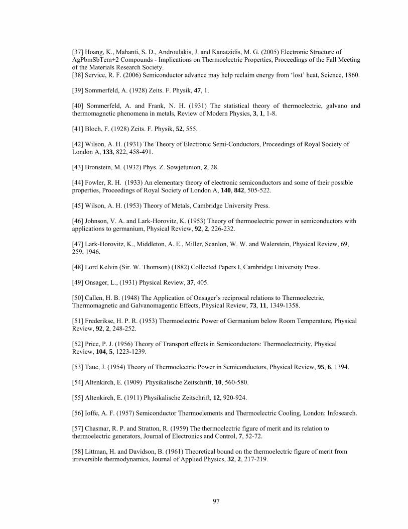
[37] Hoang, K., Mahanti, S. D., Androulakis, J. and Kanatzidis, M. G. (2005) Electronic Structure of AgPbmSbTem+2 Compounds - Implications on Thermoelectric Properties, Proceedings of the Fall Meeting of the Materials Research Society. [38] Service, R. F. (2006) Semiconductor advance may help reclaim energy from ‘lost’ heat, Science, 1860. [39] Sommerfeld, A. (1928) Zeits. F. Physik, 47, 1. [40] Sommerfeld, A. and Frank, N. H. (1931) The statistical theory of thermoelectric, galvano and thermomagnetic phenomena in metals, Review of Modern Physics, 3, 1, 1-8. [41] Bloch, F. (1928) Zeits. F. Physik, 52, 555. [42] Wilson, A. H. (1931) The Theory of Electronic Semi-Conductors, Proceedings of Royal Society of London A, 133, 822, 458-491. [43] Bronstein, M. (1932) Phys. Z. Sowjetunion, 2, 28. [44] Fowler, R. H. (1933) An elementary theory of electronic semiconductors and some of their possible properties, Proceedings of Royal Society of London A, 140, 842, 505-522. [45] Wilson, A. H. (1953) Theory of Metals, Cambridge University Press. [46] Johnson, V. A. and Lark-Horovitz, K. (1953) Theory of thermoelectric power in semiconductors with applications to germanium, Physical Review, 92, 2, 226-232. [47] Lark-Horovitz, K., Middleton, A. E., Miller, Scanlon, W. W. and Walerstein, Physical Review, 69, 259, 1946. [48] Lord Kelvin (Sir. W. Thomson) (1882) Collected Papers I, Cambridge University Press. [49] Onsager, L., (1931) Physical Review, 37, 405. [50] Callen, H. B. (1948) The Application of Onsager’s reciprocal relations to Thermoelectric, Thermomagnetic and Galvanomagentic Effects, Physical Review, 73, 11, 1349-1358. [51] Frederikse, H. P. R. (1953) Thermoelectric Power of Germanium below Room Temperature, Physical Review, 92, 2, 248-252. [52] Price, P. J. (1956) Theory of Transport effects in Semiconductors: Thermoelectricity, Physical Review, 104, 5, 1223-1239. [53] Tauc, J. (1954) Theory of Thermoelectric Power in Semiconductors, Physical Review, 95, 6, 1394. [54] Altenkirch, E. (1909) Physikalische Zeitschrift, 10, 560-580. [55] Altenkirch, E. (1911) Physikalische Zeitschrift, 12, 920-924. [56] Ioffe, A. F. (1957) Semiconductor Thermoelements and Thermoelectric Cooling, London: Infosearch. [57] Chasmar, R. P. and Stratton, R. (1959) The thermoelectric figure of merit and its relation to thermoelectric generators, Journal of Electronics and Control, 7, 52-72. [58] Littman, H. and Davidson, B. (1961) Theoretical bound on the thermoelectric figure of merit from irreversible thermodynamics, Journal of Applied Physics, 32, 2, 217-219.
97
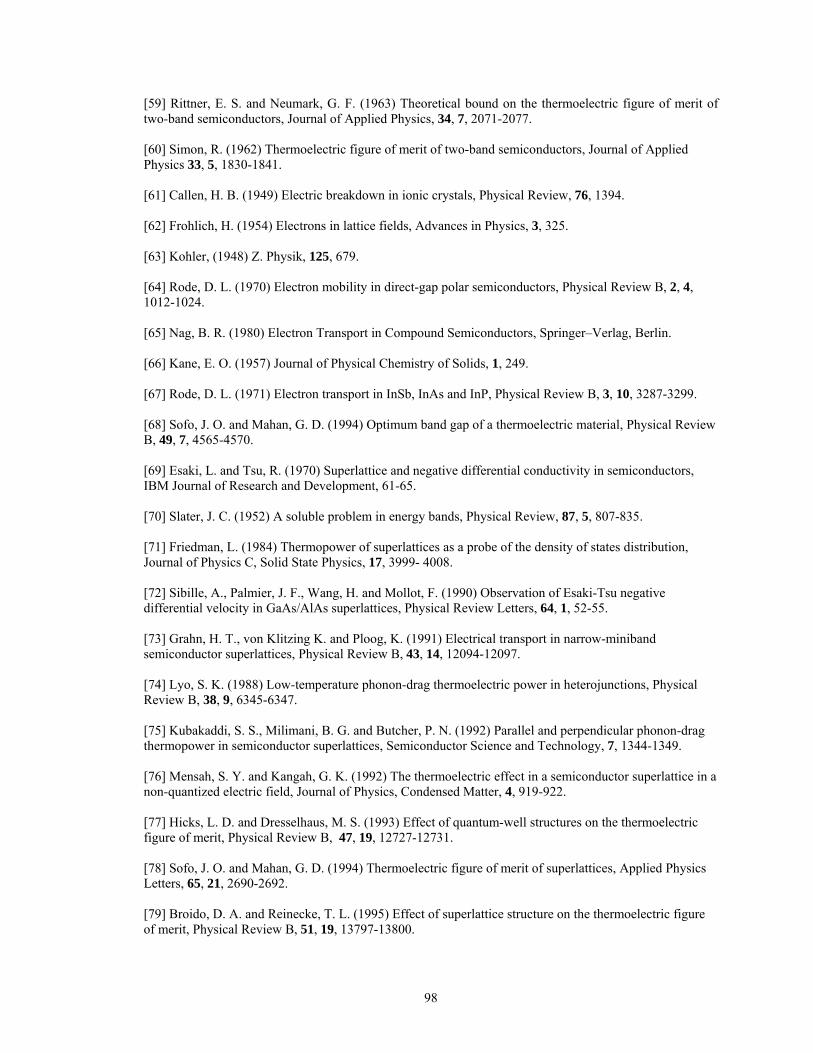
[59] Rittner, E. S. and Neumark, G. F. (1963) Theoretical bound on the thermoelectric figure of merit of two-band semiconductors, Journal of Applied Physics, 34, 7, 2071-2077. [60] Simon, R. (1962) Thermoelectric figure of merit of two-band semiconductors, Journal of Applied Physics 33, 5, 1830-1841. [61] Callen, H. B. (1949) Electric breakdown in ionic crystals, Physical Review, 76, 1394. [62] Frohlich, H. (1954) Electrons in lattice fields, Advances in Physics, 3, 325. [63] Kohler, (1948) Z. Physik, 125, 679. [64] Rode, D. L. (1970) Electron mobility in direct-gap polar semiconductors, Physical Review B, 2, 4, 1012-1024. [65] Nag, B. R. (1980) Electron Transport in Compound Semiconductors, Springer–Verlag, Berlin. [66] Kane, E. O. (1957) Journal of Physical Chemistry of Solids, 1, 249. [67] Rode, D. L. (1971) Electron transport in InSb, InAs and InP, Physical Review B, 3, 10, 3287-3299. [68] Sofo, J. O. and Mahan, G. D. (1994) Optimum band gap of a thermoelectric material, Physical Review B, 49, 7, 4565-4570. [69] Esaki, L. and Tsu, R. (1970) Superlattice and negative differential conductivity in semiconductors, IBM Journal of Research and Development, 61-65. [70] Slater, J. C. (1952) A soluble problem in energy bands, Physical Review, 87, 5, 807-835. [71] Friedman, L. (1984) Thermopower of superlattices as a probe of the density of states distribution, Journal of Physics C, Solid State Physics, 17, 3999- 4008. [72] Sibille, A., Palmier, J. F., Wang, H. and Mollot, F. (1990) Observation of Esaki-Tsu negative differential velocity in GaAs/AlAs superlattices, Physical Review Letters, 64, 1, 52-55. [73] Grahn, H. T., von Klitzing K. and Ploog, K. (1991) Electrical transport in narrow-miniband semiconductor superlattices, Physical Review B, 43, 14, 12094-12097. [74] Lyo, S. K. (1988) Low-temperature phonon-drag thermoelectric power in heterojunctions, Physical Review B, 38, 9, 6345-6347. [75] Kubakaddi, S. S., Milimani, B. G. and Butcher, P. N. (1992) Parallel and perpendicular phonon-drag thermopower in semiconductor superlattices, Semiconductor Science and Technology, 7, 1344-1349. [76] Mensah, S. Y. and Kangah, G. K. (1992) The thermoelectric effect in a semiconductor superlattice in a non-quantized electric field, Journal of Physics, Condensed Matter, 4, 919-922. [77] Hicks, L. D. and Dresselhaus, M. S. (1993) Effect of quantum-well structures on the thermoelectric figure of merit, Physical Review B, 47, 19, 12727-12731. [78] Sofo, J. O. and Mahan, G. D. (1994) Thermoelectric figure of merit of superlattices, Applied Physics Letters, 65, 21, 2690-2692. [79] Broido, D. A. and Reinecke, T. L. (1995) Effect of superlattice structure on the thermoelectric figure of merit, Physical Review B, 51, 19, 13797-13800.
98
[80] Broido, D. A. and Reinecke, T. L. (2001) Theory of thermoelectric power factor in quantum well and quantum wire superlattices, Physical Review B, 64, 045324. [81] Nag, B. R. (1980) Electron Transport in Compound Semiconductors, Springer-Verlag, Berlin. [82] Scheidemantel, T. J., Ambrosch-Draxl, C., Thonhauser, T., Badding, J. V. and Sofo, J. O. (2003) Transport coefficients from first-principles calculations, Physical Review B, 68, 125210. [83] Lee, S. and von Allmen, P. (2006) Tight-binding modeling of thermoelectric properties of bismuth telluride, Applied Physics Letters 88, 022107. [84] Datta, S. (2000) Nanoscale Device Simulation: The Green's function formalism, Superlattices and Microstructures, 28, 253-278. [85] Szafer, A. and Stone, A. D. (1989) Theory of quantum conduction through a constriction, Physical Review Letters, 62, 300-303. [86] Muller, R., Kamins, T. and Chan, M. (1986) Device Electronics for Integrated Circuits, Wiley, New York. [87] Patankar, S. V. (1980) Numerical Heat Transfer, Taylor and Francis. [88] Geballe, T. H. and Hull, G. W. (1955) Seebeck effect in silicon, Physical Review, 98, 4, 940-947. [89] Yang, B., Liu, J. L., Wang, K. L. and Chen, G. (2002) Simultaneous measurements of Seebeck coefficient and thermal conductivity across superlattice, Applied Physics Letters, 80, 10, 1758-1760. [90] Sze, S. M. (1969) Physics of Semiconductor Devices, Wiley-Interscience. [91] Choi, J. H., Park, Y. J. and Min, H. S. (1995) Electron mobility behavior in extremely thin SOI MOSFETs, IEEE Electron Device Letters, 16, 11, 527-529. [92] Takagi, S., Koga, J. and Toriumi, A. (1997) Subband structure engineering for performance enhancement of Si MOSFETs, IEEE Transactions of International Electron Devices Meeting, 219-222. [93] Wang, T., Hsieh, T. H. and Chen, T. W. (1993) Quantum confinement effects on low-dimensional electron mobility, Journal of Applied Physics, 74, 1, 426-430. [94] Fonoberov, V. A. and Balandin, A. A. (2006) Giant enhancement of the carrier mobility in silicon nanowires with diamond coating, Nano Letters, 6, 11, 2442-2446. [95] Robert, K. (2002) Explaining strain: The positive and negative effects of elastic strain in n-silicon, IEEE Circuits and Devices Magazine, 36-39. [96] Richardson, S. L., Cohen, M. L., Louie, S. G. and Chelikowsky, J. R. (1986) Electron charge densities at conduction-band edges of semiconductors, Physical Review B, Condensed Matter, 33, 2, 1177–1182. [97] Van de Walle, C. G. (1989) Band lineups and deformation potentials in the model-solid theory, Physical Review B, 39, 3, 1871-1883. [98] Yang, B. , Liu, W. L., Liu, J. L., Wang, K. L. and Chen, G. (2002) Measurements of anisotropic thermoelectric properties in superlattices, Applied Physics Letters, 81, 19, 3588-3590. [99] Yang, B., Liu, J., Wang, K. and Chen, G. (2002) Cross-plane thermoelectric properties in Si/Ge superlattices, Proceedings of the Materials Research Society, 691, G. 3. 2. 1- G. 3. 2. 6.
99
[100] Yang, B., Liu, J. L., Wang, K. L. and Chen, G. (2002) Simultaneous measurements of Seebeck coefficient and thermal conductivity across superlattice, Applied Physics Letters, 80, 10, 1758-1760. [101] Liu, W. L., Tasciuc, T. B., Liu, J. L., Taka, K., Wang, K. L., Dresselhaus, M. S. and G. Chen, (2001) In-Plane thermoelectric properties of Si/Ge superlattice, International Conference on Thermoelectrics, 340-343. [102] Vashaee, D., Zhang, Y., Zeng, G., Chiu, Y. J. and Shakouri, A. (2004) Cross-plane Seebeck coefficient anomaly in a high barrier superlattice with Miniband formation, International Conference on Thermoelectrics, Adelaide, Australia. [103] Venkatasubramanian, R., Colpitts, T., Watko, E. and Malta, D. (1997) Experimental evidence of improved thermoelectric properties at 300K in Si/Ge superlattice structures, Proceedings of Spring Meeting of the Materials Research Society, San Francisco, March 31-April 4.
100