Embed Size (px)
Citation preview
Connect Four Emulator
James Van Koevering, Kevin Weinert, Diana Szeto, Kyle Johannes Electrical and Computer Engineering Department
School of Engineering and Computer Science Oakland University, Rochester, MI
[email protected], [email protected], [email protected], [email protected]
Abstract— Connect Four is a popular strategy game
developed and marketed in 1974 by the Milton Bradley Company. The project will focus on the implementation of the game onto a Nexys 4 DDR FPGA device. The programming will require the use of a large finite state machine for positioning of the black and red chips. A combinational logic circuit will be used to check for a win. A video game controller will be used for player input. A VGA controller will be programmed to display the game onto a monitor.
I. INTRODUCTION Connect Four is a game where two players take turns
dropping black and red chips down columns in attempt to align four chips of their color in a row. The winning four can be vertical, horizontal, or diagonal.
Each player will utilize a controller to choose their desired column. Since players can win the game with any combination of their four chips in a row, the program must check each possible location. Most of the programming techniques and material required to produce the desired results of the project were discussed in class, such as logic gates, port mapping, and finite state machines. However, there is additional material that must be addressed in order to achieve success. This includes imaging using the VGA output, and wiring of a controller to the Nexys4 DDR.
II. METHODOLOGY
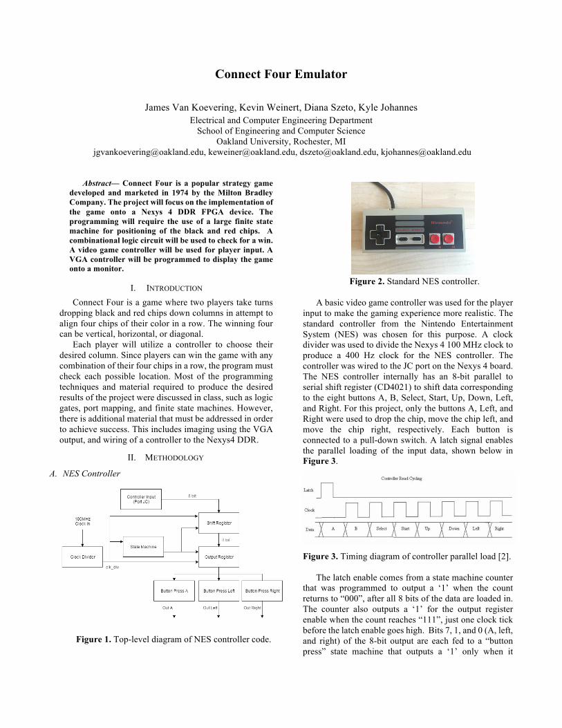
A. NES Controller
Figure 1. Top-level diagram of NES controller code.
Figure 2. Standard NES controller. A basic video game controller was used for the player
input to make the gaming experience more realistic. The standard controller from the Nintendo Entertainment System (NES) was chosen for this purpose. A clock divider was used to divide the Nexys 4 100 MHz clock to produce a 400 Hz clock for the NES controller. The controller was wired to the JC port on the Nexys 4 board. The NES controller internally has an 8-bit parallel to serial shift register (CD4021) to shift data corresponding to the eight buttons A, B, Select, Start, Up, Down, Left, and Right. For this project, only the buttons A, Left, and Right were used to drop the chip, move the chip left, and move the chip right, respectively. Each button is connected to a pull-down switch. A latch signal enables the parallel loading of the input data, shown below in Figure 3.
Figure 3. Timing diagram of controller parallel load [2]. The latch enable comes from a state machine counter
that was programmed to output a ‘1’ when the count returns to “000”, after all 8 bits of the data are loaded in. The counter also outputs a ‘1’ for the output register enable when the count reaches “111”, just one clock tick before the latch enable goes high. Bits 7, 1, and 0 (A, left, and right) of the 8-bit output are each fed to a “button press” state machine that outputs a ‘1’ only when it
detects the sequence of a user’s button press, then button release. This was implemented to obtain the user’s actual input, as well as to prevent the unintended dropping of multiple chips at once, or moving of the chip more than one column at a time. Outputs A, left, and right are then picked up as inputs by the positioning system.
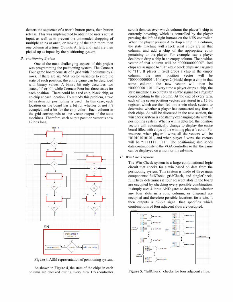
B. Positioning System One of the most challenging aspects of this project
was programming the positioning system. The Connect Four game board consists of a grid with 7 columns by 6 rows. If there are six 7-bit vector variables to store the state of each position, the entire game can be described with binary values. A binary bit only describes two states, ‘1’ or ‘0’, while Connect Four has three states for each position. There could be a red chip, black chip, or no chip at each location. To remedy this problem, a two bit system for positioning is used. In this case, each location on the board has a bit for whether or not it’s occupied and a bit for the chip color. Each column in the grid corresponds to one vector output of the state machines. Therefore, each output position vector is now 12 bits long.
Figure 4. ASM representation of positioning system. As shown in Figure 4, the state of the chips in each
column are checked during every turn. CS (controller
scroll) denotes over which column the player’s chip is currently hovering, which is controlled by the player pressing the left of right buttons on the NES controller. When the player presses A to drop a chip in a column, the state machine will check what chips are in that column, and add a chip of the appropriate color pertaining to the player. For example, say a player decides to drop a chip in an empty column. The position vector of that column will be “000000000000”. Red chips are assigned to “01” while black chips are assigned to “11”. If player 1 (red) drops a chip in the empty column, the new position vector will be “000000000001”. If player 2 (black) drops a chip in that same column, the new vector will then be “000000001101”. Every time a player drops a chip, the state machine also outputs an enable signal for a register corresponding to the column. At the end of every turn, each of the seven position vectors are stored in a 12-bit register, which are then fed into a win check system to determine whether a player has connected any four of their chips. As will be discussed in the next section, the win check system is constantly exchanging data with the positioning system. When a win is detected, the position vectors will automatically change to display the entire board filled with chips of the winning player’s color. For instance, when player 1 wins, all the vectors will be “010101010101”, and when player 2 wins, the vectors will be “111111111111”. The positioning also sends data continuously to the VGA controller so that the game can be displayed on a monitor in real-time.
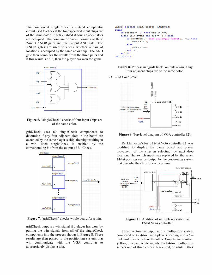
C. Win Check System The Win Check system is a large combinational logic circuit that checks for a win based on data from the positioning system. This system is made of three main components: fullCheck, gridCheck, and singleCheck. fullCheck determines if four adjacent slots in the board are occupied by checking every possible combination. It simply uses 4-input AND gates to determine whether any four slots in a row, column, or diagonal are occupied and therefore possible locations for a win. It then outputs a 69-bit signal that specifies which combinations of four adjacent slots are occupied.
Figure 5. “fullCheck” checks for four adjacent chips.
The component singleCheck is a 4-bit comparator circuit used to check if the four specified input chips are of the same color. It gets enabled if four adjacent slots are occupied. The comparator circuit consists of three 2-input XNOR gates and one 3-input AND gate. The XNOR gates are used to check whether a pair of locations is occupied by the same color chip. The AND gate then combines the results from the three pairs and if this result is a ‘1’, then the player has won the game.
Figure 6. “singleCheck” checks if four input chips are
of the same color.
gridCheck uses 69 singleCheck components to determine if any four adjacent slots in the board are occupied by the same player’s chip, thereby resulting in a win. Each singleCheck is enabled by the corresponding bit from the output of fullCheck.
Figure 7. “gridCheck” checks whole board for a win. gridCheck outputs a win signal if a player has won, by putting the win signals from all of the singleCheck components into the process shown in Figure 8. These results are then passed to the positioning system, that will communicate with the VGA controller to appropriately display a win.
Figure 8. Process in “gridCheck” outputs a win if any
four adjacent chips are of the same color.
D. VGA Controller
Figure 9. Top-level diagram of VGA controller [2].
Dr. Llamocca’s basic 12-bit VGA controller [2] was modified to display the game board and player movement of the chip in selecting the next drop location. The switch input was replaced by the seven 14-bit position vectors output by the positioning system that describe the chips in each column.
Figure 10. Addition of multiplexer system to
12-bit VGA controller.
These vectors are input into a multiplexer system composed of 49 4-to-1 multiplexers feeding into a 52-to-1 multiplexer, where the other 3 inputs are constant yellow, blue, and white signals. Each 4-to-1 multiplexer selects one of three colors: black, red, or white. Black
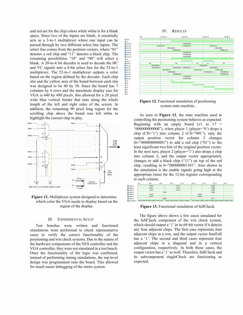
and red are for the chip colors while white is for a blank space. Since two of the inputs are blank, it essentially acts as a 3-to-1 multiplexer where one input can be passed through by two different select line inputs. The select line comes from the position vectors, where “01” denotes a red chip and “11” denotes a black chip. The remaining possibilities “10” and “00” will select a blank. A 20-to-6 bit decoder is used to decode the HC and VC signals into a 6-bit select line for the 52-to-1 multiplexer. The 52-to-1 multiplexer outputs a color based on the region defined by the decoder. Each chip slot and the yellow area of the board between each slot was designed to be 40 by 30. Since the board has 7 columns by 6 rows and the maximum display size for VGA is 640 by 480 pixels, this allowed for a 20 pixel wide blue vertical border that runs along the whole length of the left and right sides of the screen. In addition, the remaining 90 pixel long region for the scrolling chip above the board was left white to highlight the current chip in play.
Figure 11. Multiplexer system designed to determine
which color the VGA needs to display based on the region of the display.
III. EXPERIMENTAL SETUP Test benches were written and functional
simulations were performed to check representative cases to verify the correct functionality of the positioning and win check systems. Due to the nature of the hardware components of the NES controller and the VGA controller, they were not simulated in a test bench. Once the functionality of the logic was confirmed, instead of performing timing simulations, the top-level design was programmed onto the board. This allowed for much easier debugging of the entire system.
IV. RESULTS
Figure 12. Functional simulation of positioning system state machine.
As seen in Figure 12, the state machine used in
controlling the positioning system behaves as expected. Beginning with an empty board (v1 to v7 = “000000000000”), when player 1 (player=’0’) drops a chip (CD=’1’) into column 2 (CS=”001”), only the output position vector for column 2 changes (b=”000000000001”) to add a red chip (“01”) to the least significant two bits of the original position vector. In the next turn, player 2 (player=’1’) also drops a chip into column 2, and the output vector appropriately changes to add a black chip (“11”) on top of the red chip, resulting in b=”000000001101”. Also shown in the simulation is the enable signals going high at the appropriate times for the 12-bit register corresponding to each column.
Figure 13. Functional simulation of fullCheck.
The figure above shows a few cases simulated for the fullCheck component of the win check system, which should output a ‘1’ in its 69-bit vector if it detects any four adjacent chips. The first case represents four adjacent chips in a row, and the output vector fourFull has a ‘1’. The second and third cases represent four adjacent chips in a diagonal and in a vertical configuration, respectively. In both these cases, the output vector has a ‘1’ as well. Therefore, fullCheck and its subcomponent singleCheck are functioning as expected.
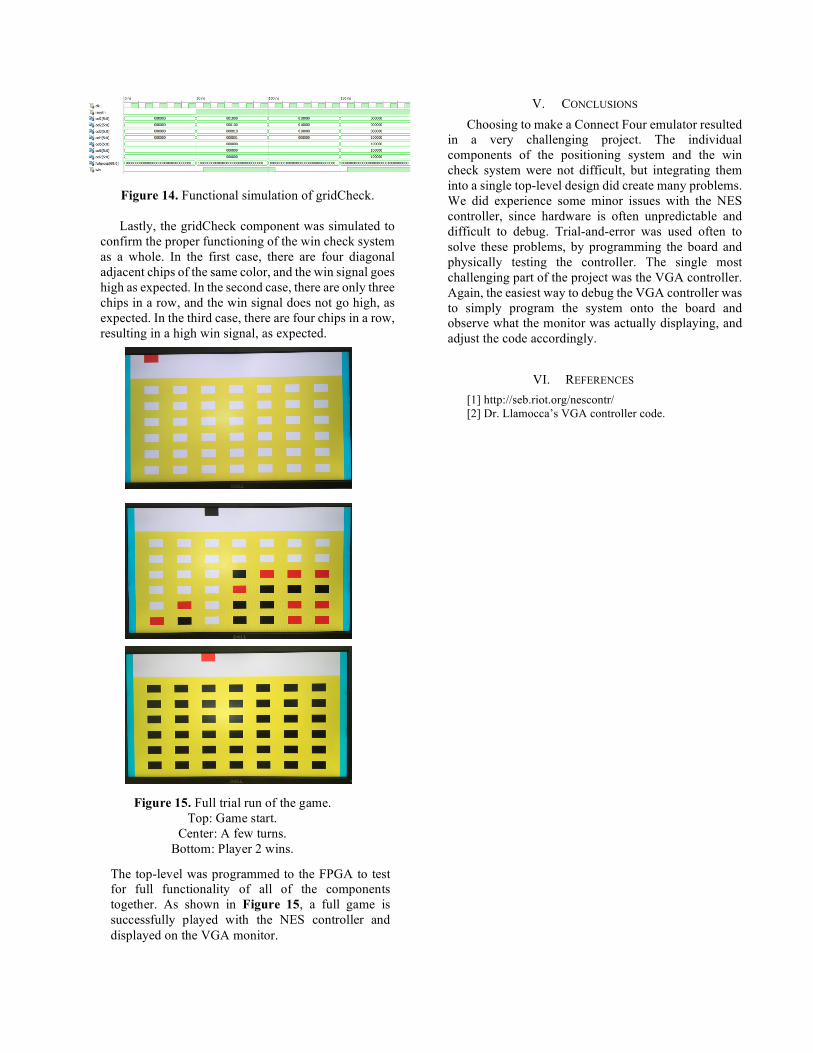
Figure 14. Functional simulation of gridCheck.
Lastly, the gridCheck component was simulated to
confirm the proper functioning of the win check system as a whole. In the first case, there are four diagonal adjacent chips of the same color, and the win signal goes high as expected. In the second case, there are only three chips in a row, and the win signal does not go high, as expected. In the third case, there are four chips in a row, resulting in a high win signal, as expected.
V. CONCLUSIONS Choosing to make a Connect Four emulator resulted
in a very challenging project. The individual components of the positioning system and the win check system were not difficult, but integrating them into a single top-level design did create many problems. We did experience some minor issues with the NES controller, since hardware is often unpredictable and difficult to debug. Trial-and-error was used often to solve these problems, by programming the board and physically testing the controller. The single most challenging part of the project was the VGA controller. Again, the easiest way to debug the VGA controller was to simply program the system onto the board and observe what the monitor was actually displaying, and adjust the code accordingly.
VI. REFERENCES [1] http://seb.riot.org/nescontr/ [2] Dr. Llamocca’s VGA controller code.
Figure 15. Full trial run of the game. Top: Game start.
Center: A few turns. Bottom: Player 2 wins.
The top-level was programmed to the FPGA to test for full functionality of all of the components together. As shown in Figure 15, a full game is successfully played with the NES controller and displayed on the VGA monitor.