Embed Size (px)
Citation preview
Configuring the Élan ™SC300 Device’s InternalCGA Controller for a Specific LCD Panel
Application Note
This application note explains how to determine if a specific LCD panel is supported by theÉlanTMSC300 microcontroller, and in what modes (CGA two-color or four-color graphics, CGA text,HGA graphics, HGA text); how to configure the ÉlanSC300 microcontroller to work with the LCDpanel in those modes; and which signals need to be connected to the ÉlanSC300 microcontrollerto properly drive the panel.INTRODUCTIONThere are a number of factors that need to be under-stood to accomplish the tasks mentioned above. Thesections in the first part of this document provide youwith the understanding and background needed to fol-low the procedures beginning on page 7. You are alsoencouraged to read and have available for referenceChapter 3, “Video Controller” of the ÉlanTMSC300 Mi-crocontroller Programmer’s Reference Manual, order#18470.
DEFINITIONSThe following terms are used throughout this docu-ment. Understanding these terms as they apply to theÉlanSC300 microcontroller is essential for understand-ing how to configure the microcontroller’s Video Indexregisters to work with various LCD panels.
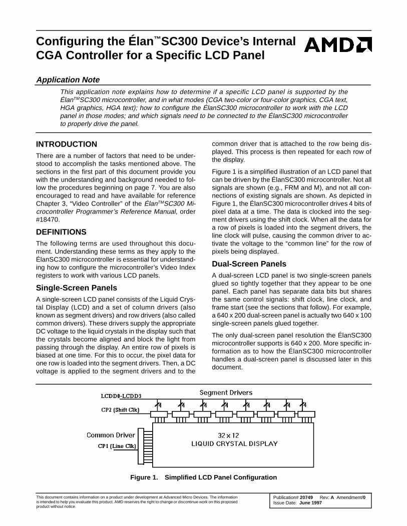
Single-Screen PanelsA single-screen LCD panel consists of the Liquid Crys-tal Display (LCD) and a set of column drivers (alsoknown as segment drivers) and row drivers (also calledcommon drivers). These drivers supply the appropriateDC voltage to the liquid crystals in the display such thatthe crystals become aligned and block the light frompassing through the display. An entire row of pixels isbiased at one time. For this to occur, the pixel data forone row is loaded into the segment drivers. Then, a DCvoltage is applied to the segment drivers and to the
common driver that is attached to the row being dis-played. This process is then repeated for each row ofthe display.
Figure 1 is a simplified illustration of an LCD panel thatcan be driven by the ÉlanSC300 microcontroller. Not allsignals are shown (e.g., FRM and M), and not all con-nections of existing signals are shown. As depicted inFigure 1, the ÉlanSC300 microcontroller drives 4 bits ofpixel data at a time. The data is clocked into the seg-ment drivers using the shift clock. When all the data fora row of pixels is loaded into the segment drivers, theline clock will pulse, causing the common driver to ac-tivate the voltage to the “common line” for the row ofpixels being displayed.
Dual-Screen PanelsA dual-screen LCD panel is two single-screen panelsglued so tightly together that they appear to be onepanel. Each panel has separate data bits but sharesthe same control signals: shift clock, line clock, andframe start (see the sections that follow). For example,a 640 x 200 dual-screen panel is actually two 640 x 100single-screen panels glued together.
The only dual-screen panel resolution the ÉlanSC300microcontroller supports is 640 x 200. More specific in-formation as to how the ÉlanSC300 microcontrollerhandles a dual-screen panel is discussed later in thisdocument.
Figure 1. Simplified LCD Panel Configuration
Publication# 20749 Rev: A Amendment/0Issue Date: June 1997
This document contains information on a product under development at Advanced Micro Devices. The informationis intended to help you evaluate this product. AMD reserves the right to change or discontinue work on this proposedproduct without notice.

Pixel ClockThis is the standard unit of measure from which all ofthe LCD clocking signals can be derived. The pixelclock can be loosely defined as the rate at which pixelsare displayed on the screen. On the ÉlanSC300 micro-controller, the pixel clock used is one of two fixed fre-quencies: 14.336 MHz for HGA mode or 9.557 MHz(which is 2/3 of 14.336) for CGA mode. On theÉlanSC300 microcontroller, the pixel clock is internal tothe video controller and is not available external to thechip.
Shift Clock (CP2)The shift clock, known as the CP2 signal on theÉlanSC300 microcontroller, tells the LCD panel whendata is valid on the LCD data bus (the ÉlanSC300 mi-crocontroller pins LCDD0–LCDD3 and LCDDL0–LCDDL3). Data is valid on the falling edge of shift clock.
The frequency of the shift clock can be determined bythe pixel clock frequency divided by the number of databits per panel. For both single- and dual-screen panelswith the ÉlanSC300 microcontroller, the number of bitsper panel is four. Therefore, the shift clock frequencywill be either 14.336 MHz ÷ 4 data bits = 3.58 MHz, or9.557 MHz ÷ 4 data bits = 2.389 MHz.
Line Clock (CP1)The line clock, known as the CP1 signal on theÉlanSC300 microcontroller, tells the LCD panel that acomplete row (horizontal line) of pixel data has beensent to the LCD panel to be displayed. Additional shiftclocks indicate valid data for the next row of pixels (i.e.,display the current row and prepare to receive pixeldata for the next row).
A line clock pulse will occur once for every row of pixeldata sent to the LCD panel. For example, a 320 x 240LCD screen has 240 rows; therefore, 240 line clockswill occur each time the panel is refreshed.
When CP1 is asserted on the ÉlanSC300 microcontrol-ler’s LCD controller, there is a period of about 20 pixelclock cycles during which CP2 will not be asserted.This has a slight effect on the refresh rate as describedlater in this document.
Frame Start (FRM) Frame start, known as FRM on the ÉlanSC300 micro-controller, is asserted at the start of every frame (panelscan). This signal tells the LCD panel that the next datasent to it via the shift clock will be for the top row of thepanel. This signal is sometimes referred to as the FLM(First Line Marker) signal.
On the ÉlanSC300 microcontroller’s LCD controller,there is no “dead time” when FRM is asserted. TheFRM assertion overlaps with the normal CP1 assertionat the end of the last line.
Refresh RateThe refresh rate of the LCD panel is the number oftimes per second the screen is redrawn. This affectsthe crispness and brightness of the image on the dis-play. On the ÉlanSC300 microcontroller, the refreshrate is affected by the screen resolution programmedinto the video controller, the number of bits per pixel(BPP) (in Graphics mode only), and the pixel clock fre-quency.
On the ÉlanSC300 microcontroller, the refresh rate forText mode or 2-color Graphics mode can be calculatedby dividing the pixel clock frequency by the screen res-olution programmed into the video controller, takinginto account the 20 extra pixel clocks per line men-tioned in the previous section. The refresh rate for 4-color Graphics mode will be half that amount. For ex-ample, if the controller is programmed for a 320 x 240LCD screen and configured for CGA 2-color mode(which means that the 9.557 MHz pixel clock is used),then each line consists of 320 + 20 = 340 pixel clocks,and the refresh rate would be 9.557 MHz ÷ (340 · 240)= 117.1 Hz.
If the refresh rate is marginal for the LCD size in CGAGraphics mode, a 50% increase in refresh rate can beachieved by using HGA Graphics mode. On theÉlanSC300 microcontroller, the selection of CGA orHGA mode can remain independent of the resolution.(This is discussed later in this document.)
DC Voltage BiasingDC voltage biasing is a condition of LCD panels whenthe liquid crystals in the display become permanentlyaligned. Normally, the liquid crystals are nonaligned, al-lowing light to pass through the display. When a DCvoltage is applied, the liquid crystals align themselves,blocking the light from passing through the display. Theeffect of this alignment causes a pixel to appear darkon the display. As a panel becomes DC voltage biased,the liquid crystals in the display become permanentlyaligned, eventually causing the entire display to appearblack. AC modulation (defined in the next section) isused to prevent DC biasing.
LCD Panel AC Modulation (M)All LCD panels implement what is known as AC modu-lation to prevent DC voltage biasing from damaging thedisplay. AC modulation is accomplished by periodicallyreversing the polarity of the DC voltage that is appliedto the liquid crystals. This prevents the crystals frombecoming permanently aligned. Some panels controlthe frequency at which the polarity is reversed inter-nally. Other panels require an outside source to controlthis. For panels requiring an outside source to imple-ment this control, the ÉlanSC300 microcontroller sup-plies an AC modulation signal, M. This signal can beprogrammed to change state once per frame, onceevery 13 line clocks, or once every 61 line clocks.
2 Configuring the Élan™SC300 Device’s Internal CGA Controller for a Specific LCD Panel
Gray Shading (Gray Scaling)Gray shading is a way of representing colors on amonochrome LCD display using shades of gray. TheIRGB color information for each pixel is used to deter-mine which gray shading algorithm will be used to dis-play that pixel. The gray shading algorithm can bethought of as the duty cycle for displaying a particularpixel. For example, on the ÉlanSC300 microcontroller,an IRGB value of 1011 corresponds to a 1/3 duty cycle.This means that, if a pixel is supposed to be displayed,it would be displayed once for every three times thescreen is refreshed. Refer to Table 3 on page 6 for a listof the ÉlanSC300 microcontroller’s IRGB values andtheir corresponding gray shading duty cycles.
ÉlanSC300 MICROCONTROLLER EXTENSIONS TO THE CGA AND HGA STANDARDS
CGA StandardThe CGA standard was defined for a color CRT monitorwith a resolution of 640 x 200 pixels. The CGA stan-dard defines two graphic resolutions:
1. 640 x 200 pixels, with two colors, represented by1 BPP.
2. 320 x 200 pixels, with four colors, represented by2 BPP. In 320 x 200 mode, each pixel in the x di-mension is displayed twice.
For both 640 x 200 and 320 x 200 resolutions, thememory is divided into two 8-Kbyte banks. Pixel datafor even-numbered display rows (starting with 0) arestored in bank 0, address range B8000–B9FFF. Pixeldata for odd-numbered display rows are stored in bank1, address range BA000–BBFFF. The Graphics modesection of Chapter 3 in the ÉlanTMSC300 Microcontrol-ler Programmer’s Reference Manual helps illustratethis.
In Text mode, 16 colors are available for characters. Textmode is discussed in detail in Chapter 3 of theÉlanTMSC300 Microcontroller Programmer’s ReferenceManual and follows the CGA standard implementation;therefore, it will not be discussed in detail in this docu-ment.
How the ÉlanSC300 Microcontroller Deviates from the CGA Standard The ÉlanSC300 microcontroller can support any com-bination of resolutions at either 1 or 2 BPP (two or fourcolors), provided the video SRAM requirements do notexceed 32 Kbyte. For memory requirements greaterthan 16 Kbyte, the ÉlanSC300 microcontroller can beprogrammed to use three, or even all four, of the 8-Kbyte banks of video SRAM. If all four banks are used:
■ The pixel data for display rows 0, 4, 8,... are inbank 1 (address range B8000–B9FFF).
■ The pixel data for display rows 1, 5, 9,... are inbank 2 (address range BA000–BBFFF).
■ The pixel data for display rows 2, 6, 10,... are inbank 3 (address range BC000–BDFFF).
■ The pixel data for display rows 3, 7, 11,... are inbank 4 (address range BE000–BFFFF).
Note that two banks are the minimum. Thus, even if thepixel data for a small LCD screen could fit in 8 Kbyte(for example, 320 x 200 in 2-color mode), two banksmust still be used.
In 4-color Graphics mode (2 BPP), it is possible to se-lect whether or not pixels are doubled in the x dimen-sion. (In the CGA standard, the pixel doubling isautomatic in 4-color Graphics mode.) If the ÉlanSC300microcontroller graphics control is set to display 2-BPPgraphics (Port 3D8h bit 4 = 0), and if Video Index 20hbit 5 = 0, two pixels are displayed, effectively cutting thehorizontal resolution in half. If Video Index 20hbit 5 = 1, only one pixel is displayed.
In CGA Text mode, the ÉlanSC300 microcontroller getsits fonts from SRAM rather than ROM and can supportmultiple font areas. The character width is fixed at eightpixels, but the character height is programmable. Theway the font areas are addressed is discussed in detailin Chapter 3 of the ÉlanTMSC300 Microcontroller Pro-grammer’s Reference Manual.
HGA StandardThe HGA standard was defined for a high-resolution,monochrome CRT with a resolution of 720 x 348 pixels.In Graphics mode, this allows two colors (black andwhite) represented by 1 BPP. The standard implemen-tation is to use four 8-Kbyte banks of video SRAM inthe same way the ÉlanSC300 microcontroller handlesthe four-bank CGA configuration. In the case of HGA,the standard address range for bank 1 is B0000–B1FFF, for bank 2 it is B2000–B3FFF, for bank 3 it isB4000–B5FFF, and for bank 4 it is B6000–B7FFF. TheHGA standard also supports a second 32-Kbyte dis-play page at B8000.
In Text mode, three character colors are available:black, light gray, and white.
How the ÉlanSC300 Microcontroller Deviates from the HGA StandardThe ÉlanSC300 microcontroller can support any com-bination of resolutions, provided the video SRAM re-quirements do not exceed 32 Kbyte. For memoryrequirements of 16 Kbyte or less, the ÉlanSC300 mi-crocontroller can be configured to use only two 8-Kbytebanks of memory. For memory requirements of 16–24 Kbyte, the ÉlanSC300 microcontroller can be con-figured to use only three 8-Kbyte banks of memory.
Configuring the Élan™SC300 Device’s Internal CGA Controller for a Specific LCD Panel 3
Although the HGA standard supports two 32-Kbyte dis-play pages, only 32 Kbyte of video SRAM are availableon the ÉlanSC300 microcontroller. Therefore, theÉlanSC300 microcontroller will only allow access toB0000–B7FFF in HGA mode.
In HGA Text mode, the ÉlanSC300 microcontroller getsits fonts from SRAM rather than ROM. The characterwidth is fixed at nine pixels (the 9th column being auto-matically generated), but the character height is pro-grammab le . Chapter 3 o f the É lan T M SC300Microcontroller Programmer’s Reference Manual de-tails the way the font areas are addressed.
MEMORY MAP ORGANIZATION FOR VARIOUS DISPLAY MODES AND PANEL SIZESIt is important to understand which settings affect thememory map of the video SRAM. This will enable youto properly display information on the screen. Chapter3 of the ÉlanTMSC300 Microcontroller Programmer’sReference Manual explains the memory map for Textmode, how fonts should be set up, and how characterand attribute bytes are organized. It also explainsmemory maps for a few different display sizes forGraphics modes. This section expands on the informa-tion found in the ÉlanTMSC300 Microcontroller Pro-grammer’s Reference Manual. It is meant to show howscreen size and number of banks of video memory—bits per pixel (graphics) and font size (text)— affect thedisplay data memory area.
Text ModeIn Text mode, the display data area is 16 Kbyte (forCGA, B8000h–BBFFFh and for HGA, B0000h–B3FFFh). Some of the remaining 16 Kbyte of the dis-play area are used for four different font areas, threeof which are available in CGA Text mode and one ofwhich is available in HGA Text mode. Refer toSection 3.4 “Text Mode,” in the ÉlanTMSC300 Micro-controller Programmer’s Reference Manual, for Textmode memory map examples.
Graphics ModeIn Graphics mode, the video SRAM memory map is de-termined by the LCD resolution programmed into the
ÉlanSC300 microcontroller, the number of banks ofmemory selected, and the number of bits per pixel re-quired. Refer to Section 3.3, “Graphics Mode,” in theÉlanTMSC300 Microcontroller Programmer’s Refer-ence Manual, for Graphics mode memory map exam-ples.
In Graphics mode, the video SRAM memory is split into8-Kbyte banks. Either two or four 8-Kbyte banks areused. Refer to "Steps for Determining if a Single-Screen LCD Panel can be Driven by the ÉlanSC300Microcontroller" on page 7 to determine how manybanks are needed. The display rows are split evenlyacross the banks, as illustrated in the tables on the fol-lowing page.
The number of bits per pixel and the programmedscreen width determine how many bytes of data perrow are needed. For example, a 128-pixel-wide screen,at 2 BPP needs 2 · 128 = 256 bits of data per row, and256 ÷ 8 = 32 bytes of data per row. At 2 bits per pixel,each pixel can be set to one of four colors. A 128-pixel-wide screen at 1 BPP needs 1 · 128 = 128 bits of dataper row, and 128 ÷ 8 = 16 bytes of data per row. At1 BPP, each pixel can be set to only one of two colors.Thus, more colors require more memory.
Note: With smaller panels, it may be necessary to pro-gram the ÉlanSC300 microcontroller’s graphics con-troller with a logical screen width greater than thephysical screen width of the LCD panel to meet thepanel’s refresh rate requirements. Reminder: if this isdone, it is the logical screen width programmed into thegraphics controller that determines the number of bytesper row.
The following tables illustrate the memory map for a128 x 128 pixel display set up for 2 BPP, in both atwo-bank and four-bank configuration. As shown inthe tables, a 128-pixel-wide display at 2 BPP re-quires 32 bytes of memory per row. If the width ofthe display were to increase or decrease, thechange would cause the row ending address andsubsequent starting addresses to increase or de-crease, respectively.
4 Configuring the Élan™SC300 Device’s Internal CGA Controller for a Specific LCD Panel
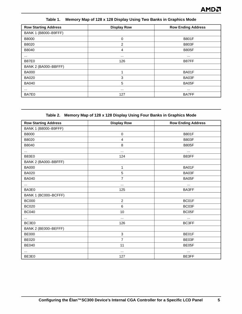
Table 1. Memory Map of 128 x 128 Display Using Two Banks in Graphics Mode
Table 2. Memory Map of 128 x 128 Display Using Four Banks in Graphics Mode
Row Starting Address Display Row Row Ending Address
BANK 1 (B8000–B9FFF)
B8000 0 B801F
B8020 2 B803F
B8040 4 B805F
... ... ...
B87E0 126 B87FF
BANK 2 (BA000–BBFFF)
BA000 1 BA01F
BA020 3 BA03F
BA040 5 BA05F
... ... ...
BA7E0 127 BA7FF
Row Starting Address Display Row Row Ending Address
BANK 1 (B8000–B9FFF)
B8000 0 B801F
B8020 4 B803F
B8040 8 B805F
... ... ...
B83E0 124 B83FF
BANK 2 (BA000–BBFFF)
BA000 1 BA01F
BA020 5 BA03F
BA040 7 BA05F
... ... ...
BA3E0 125 BA3FF
BANK 1 (BC000–BCFFF)
BC000 2 BC01F
BC020 6 BC03F
BC040 10 BC05F
... ... ...
BC3E0 126 BC3FF
BANK 2 (BE000–BEFFF)
BE000 3 BE01F
BE020 7 BE03F
BE040 11 BE05F
... ... ...
BE3E0 127 BE3FF
Configuring the Élan™SC300 Device’s Internal CGA Controller for a Specific LCD Panel 5
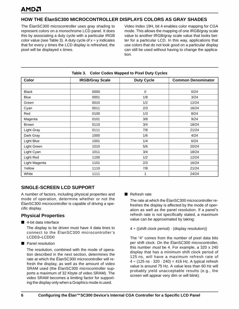
HOW THE ÉlanSC300 MICROCONTROLLER DISPLAYS COLORS AS GRAY SHADESThe ÉlanSC300 microcontroller uses gray shading torepresent colors on a monochrome LCD panel. It doesthis by associating a duty cycle with a particular IRGBcolor value (see Table 3). A duty cycle of x ÷ y indicatesthat for every y times the LCD display is refreshed, thepixel will be displayed x times.
Video Index 19H, bit 4 enables color mapping for CGAmode. This allows the mapping of one IRGB/gray scalevalue to another IRGB/gray scale value that looks bet-ter for a particular LCD. In this way, applications thatuse colors that do not look good on a particular displaycan still be used without having to change the applica-tion.
SINGLE-SCREEN LCD SUPPORTA number of factors, including physical properties andmode of operation, determine whether or not theÉlanSC300 microcontroller is capable of driving a spe-cific display.
Physical Properties■ 4-bit data interface
The display to be driven must have 4 data lines toconnect to the ÉlanSC300 microcontroller ’sLCDD3–LCDD0
■ Panel resolution
The resolution, combined with the mode of opera-tion described in the next section, determines therate at which the ÉlanSC300 microcontroller will re-fresh the display, as well as the amount of videoSRAM used (the ÉlanSC300 microcontroller sup-ports a maximum of 32 Kbyte of video SRAM). Thevideo SRAM becomes a limiting factor for support-ing the display only when a Graphics mode is used.
■ Refresh rate
The rate at which the ÉlanSC300 microcontroller re-freshes the display is affected by the mode of oper-ation as well as the panel resolution. If a panel’srefresh rate is not specifically stated, a maximumvalue can be approximated by taking:
4 ÷ ((shift clock period) · (display resolution))
The “4” comes from the number of pixel data bitsper shift clock. On the ÉlanSC300 microcontroller,this number must be 4. For example, a 320 x 240display that has a minimum shift clock period of125 ns, will have a maximum refresh rate of4 ÷ (125 ns · 320 · 240) = 416 Hz. A typical refreshvalue is around 75 Hz. A value less than 60 Hz willprobably yield unacceptable results (e.g., thescreen will appear very dim or will blink).
Table 3. Color Codes Mapped to Pixel Duty Cycles
Color IRGB/Gray Scale Duty Cycle Common Denominator
Black 0000 0 0/24
Blue 0001 1/8 3/24
Green 0010 1/2 12/24
Cyan 0011 2/3 16/24
Red 0100 1/3 8/24
Magenta 0101 3/8 9/24
Brown 0110 3/4 18/24
Light Gray 0111 7/8 21/24
Dark Gray 1000 1/6 4/24
Light Blue 1001 1/4 6/24
Light Green 1010 5/6 20/24
Light Cyan 1011 3/4 18/24
Light Red 1100 1/2 12/24
Light Magenta 1101 2/3 16/24
Yellow 1110 7/8 21/24
White 1111 1 24/24
6 Configuring the Élan™SC300 Device’s Internal CGA Controller for a Specific LCD Panel

Mode of operationThe mode of operation affects the refresh rate of thedisplay, and when a Graphics mode is selected, deter-mines the amount of video SRAM required. When theÉlanSC300 microcontroller is configured for a Graphicsmode, the 32 Kbyte of memory is divided into four 8-Kbyte banks. Video Index register 09H controlswhether the display information is divided between justtwo or all four of the memory banks.
■ CGA Mode
When CGA mode is selected, the ÉlanSC300 mi-crocontroller uses a pixel clock frequency of9.557 MHz. The refresh rate for Text mode, or 2-color Graphics mode can be calculated by dividing
the pixel clock frequency by the screen resolutionprogrammed into the video controller, taking into ac-count the 20 extra pixel clocks per line mentionedearlier. The refresh rate for 4-color Graphics modewill be half that value.
■ HGA Mode
When HGA mode is selected, the ÉlanSC300 mi-crocontroller uses a pixel clock frequency of14.336 MHz. The refresh rate for Text mode or 2-color Graphics mode can be calculated by dividingthe pixel clock frequency by the screen resolutionprogrammed into the video controller, taking into ac-count the 20 extra pixel clocks per line mentionedearlier.
STEPS FOR DETERMINING IF A SINGLE-SCREEN LCD PANEL CAN BE DRIVEN BY THE ÉlanSC300 MICROCONTROLLER1. Does the panel have a 4-bit data interface?
– Yes: Go to step 2.
– No: Panel cannot be driven by the ÉlanSC300microcontroller.
2. Determine what rate the ÉlanSC300 microcontrollerwill refresh the LCD panel. Refresh rate is a factorof the LCD panel resolution and pixel clock fre-quency, which is determined by the mode of opera-tion. For a panel size of W x H, and a bits-per-pixelvalue of BPP (1 or 2), the refresh rate will be as fol-lows:
(pixel clock frequency) ÷ ((W + 20) · BPP · H)
In CGA mode, the pixel clock frequency is9.557 MHz. In HGA mode the pixel clock frequencyis 14.336 MHz. Therefore, when the ÉlanSC300 mi-crocontroller is configured for a 320 x 240, 1-BPPresolution LCD in CGA mode, the refresh rate is9.557 MHz ÷ (340 · 1 · 240) = 117 Hz. When theÉlanSC300 microcontroller is configured for thesame size display in HGA mode, the refresh rate is14.336 MHz ÷ (340 · 1 · 240) = 175 Hz. Note that 2-color (1 BPP) mode can be supported by eitherCGA or HGA, but the HGA refresh rate is approxi-mately 50% higher.
3. Does the refresh rate fall in the range supported bythe LCD panel?
– Yes: Go to step 4.
– No: Panel cannot be driven by the ÉlanSC300 microcontroller.
Note: If the refresh rate driven by the ÉlanSC300 mi-crocontroller is too fast for the panel, it is possible to ef-fectively slow the refresh rate to the panel byprogramming the ÉlanSC300 microcontroller’s graph-ics controller using a logical panel width that is greaterthan the physical LCD panel width. If this is done, the
logical panel width must be used for all calculations,and it should first be tested on the same panel beforemaking the design choice. This will determine if thepanel can handle the additional shift clocks sent to it asa result of the larger panel width.
4. Does the ÉlanSC300 microcontroller support theLCD panel’s video SRAM requirements?
This is a concern only if the LCD will be operated ina Graphics mode; therefore, Text mode is not dis-cussed.
2 bits per pixel (four shades of gray)This mode consumes the most memory. Each bankof memory is 8 Kbyte (8192 bytes). In 2 BPP mode,each byte contains the equivalent of 4 pixels of in-formation. Each bank can store information for32,768 pixels. Therefore, if configured for 4 banksof memory, the maximum number of pixels that theÉlanSC300 microcontroller can support is 4 ·32,768 = 131,072 pixels. If configured for two banksof memory, the maximum number of pixels that theÉlanSC300 microcontroller can support is 2 ·32,768 = 65,536 pixels.
For example: a 320 x 240 LCD display has320 · 240 = 76 ,800 p ixe ls . Therefore, theÉlanSC300 microcontroller will support this resolu-tion LCD if configured for four banks of memory.
1 bit per pixel (2 shades of gray)Each bank of memory is 8 Kbyte (8192 bytes). In1 BPP mode, each byte contains the equivalent of 8pixels of information. Each bank can store informa-tion for 65,536 pixels. Therefore, if configured forfour banks of memory, the maximum number of pix-els that the ÉlanSC300 microcontroller can supportis 4 · 65,536 = 262,144 pixels. If configured for twobanks of memory, the maximum number of pixels
Configuring the Élan™SC300 Device’s Internal CGA Controller for a Specific LCD Panel 7
that the ÉlanSC300 microcontroller can support is2 · 65,536 = 131,072 pixels.For example: a 640 x 400 LCD display has640 · 400 = 256,000 p ixels . Therefore the
ÉlanSC300 microcontroller will support this resolu-tion LCD if configured for four banks of memory.
5. If the LCD panel meets the criteria listed in the pre-vious four steps, then the ÉlanSC300 microcontrol-ler is capable of driving the LCD panel.
PROGRAMMING THE ÉlanSC300 MICROCONTROLLER TO WORK WITH A SINGLE-SCREEN LCD PANELBefore programming the ÉlanSC300 microcontroller towork with a single-screen LCD panel, the following in-formation is needed:
■ Display resolution in pixels, W x H (e.g., 640 x 200)
■ Mode of operation (i.e., CGA graphics-1 BPP, CGAgraphics-2 BPP, CGA text, HGA graphics-1 BPP,HGA text)
■ If Text mode, the font size (8 x FH for CGA or 9 x FHfor HGA, where FH = font height; 8 x 8 is CGA stan-dard, 9 x 14 is HGA standard)
■ If Graphics mode, the number of 8-Kbyte banks ofmemory (see "Steps for Determining if a Single-Screen LCD Panel can be Driven by the ÉlanSC300Microcontroller" on page 7)
Determine the Video Index Values to Be ProgrammedFirst determine the Video Index values for Video In-dexes 00–0Fh, based on the information listed in thefour items above.
CGA & HGA Graphics Mode Values
■ (HT = W · BPP ÷ 16)
The Horizontal Total Register (Index 00H) and Hor-izontal Displayed Register (Index 01H) are pro-grammed with the number of 16-bit words perdisplay row. In 2-color mode (1 BPP), this equalsthe width of the display in pixels divided by 16. In 4-color mode (2 BPP), this equals two times the widthof the display in pixels divided by 16. For example,a 320 x 240 display is 320 pixels wide. Therefore, in2-color mode (1 BPP), HT = 320 ÷ 16 = 20 (14h).
■ (VT = H ÷ BANKS)
The Vertical Total Register (Index 04H), VerticalDisplay Register (Index 06H), and Vertical Sync Po-sition Register (Index 07H) are programmed withthe value of the height of the display in pixels, di-vided by the number of banks of memory. For exam-ple, a 320 x 240 display is 240 pixels high. If fourbanks of memory are going to be used, then VT =240 ÷ 4 = 60 (3Ch).
■ (MSL = BANKS – 1)
The Max Scan Line Register (Index 09H) is pro-grammed with the number of banks of memory tobe used, minus 1. If four banks of memory are goingto be used, then MSL = 4 – 1 = 3.
■ (SAH) (SAL)
The Start Address High (Index 0CH) and Start Ad-dress Low (Index 0DH) Video Indexes togetherform a 14-bit offset (bits 7 and 6 of Index 0CH arenot used) that determines the location in videomemory where the video controller will start fetchingdata to be displayed on the screen. Typically, theseindexes will be set to 0 so the display data startsbeing fetched from B8000h. Scrolling can be imple-mented by changing the values in these registers.
■ All the other index registers (02, 03, 05, 08, 0Ah,0Bh, 0Eh, 0Fh) will be programmed with 0h.
CGA & HGA Text Mode Values
■ HT = W · BPP ÷ 16
The Horizontal Total Register (Index 00H) and Hor-izontal Displayed Register (Index 01H) are pro-grammed with the number of characters per row.The character width is hard coded to be 8 pixelswide. Therefore, HT is the width of the display in pix-els divided by 8. For example, a 320 x 240 displayis 320 pixels wide. Therefore HT = 320 ÷ 8 = 40(28h).
■ (VT = H ÷ Y)
The Vertical Total Register (Index 04H), VerticalDisplayed Register (06H), and Vertical Sync Posi-tion Register (07H) are programmed with the valueof the number of rows of characters. This is deter-mined by the height of the display in pixels, dividedby the height of the character in pixels (Y from theequation below). For example, a 320 x 240 displayis 240 pixels high. If using an 8 x 10 font, then VT =240 ÷ 10 = 24 (18h).
■ (MSL = Y –1)
The Max Scan Line Register (Index 09H) is pro-grammed with the pixel height of the font – 1. Forexample, if using an 8 x 10 font, then MSL =10 – 1 = 9.
8 Configuring the Élan™SC300 Device’s Internal CGA Controller for a Specific LCD Panel

■ (CS = Cursor Start Row –1)(CE = Cursor End Row –1)
The Cursor Start Register (Index 0AH), and CursorEnd Register (Index 0BH) define the pixel rowswithin a font where the cursor will be displayed. Typ-ically, the cursor is defined to be near the bottom ofthe character matrix. For example, an 8 x 10 fonthas 10 pixel rows. Therefore, to have the cursor po-sitioned at rows 8 and 9, CS = 8 – 1 = 7, and CE =9 – 1 = 8.
Note: Bits 6 and 5 of the Cursor Start Register (Index0AH) control the cursor’s behavior. See Table 4.
■ (SAH) (SAL)
The Start Address High (Index 0CH) and Start Ad-dress Low (Index 0DH) Video Indexes togetherform a 14-bit offset (bits 7 and 6 of Index 0CH arenot used) that determines the location in videomemory where the video controller will start fetchingdata to be displayed on the screen. Typically, theseindexes will be set to 0 so the display data startsbeing fetched from B8000h. Scrolling can be imple-mented by changing the values in these registers.
■ (CAH) (CAL)
Cursor Address High (Index 0EH) and Cursor Ad-dress Low (Index 0FH) Video Indexes together forma 14-bit offset (bits 7 and 6 of Index 0CH are notused) that determines the location in video memorywhere the video controller will display the cursorwhen the corresponding video data is displayed onthe screen. For example, if SAH = 0, SAL = 0, CAH= 0, and CAL = 0, the cursor will be displayed in theupper left corner of the screen.
■ All the other index registers (02, 03, 05, 08, 0Ah,0Bh, 0Eh, 0Fh) will be programmed with 0h.
Initializing the Video ControllerThe following sequences show the proper sequencefor initializing the video controller. The following stepsassume the video controller is set up to its default modeof CGA and the Video Index registers are unlocked. (Tounlock the video registers, write 12h to Port 3D4h, andread Port 3D5h with no I/O cycles between these.)
Note: Only the minimum set of registers required toget the screen running are initialized. There are a num-ber of additional features such as auto screen blankingand text truncat ion that are discussed in the
ÉlanSC300 Microcontroller Programmer’s ReferenceManual that are not reiterated in this document.
CGA GraphicsThe Video Index registers are accessed by writing theregister index to Port 3D4h, and then writing or readingthe register data to or from Port 3D5h.
1. Set Video Index 18H = 50h
– Sets up LCD panel type to single screen (bits 7and 6)
– Sets display type to LCD (bit 4)
2. Set Video Index 00H = HT
3. Set Video Index 01H = HT
4. Set Video Index 02H = 0
5. Set Video Index 03H = 0
6. Set Video Index 04H = VT
7. Set Video Index 05H = 0
8. Set Video Index 06H = VT
9. Set Video Index 07H = VT
10.Set Video Index 08H = 0
11.Set Video Index 09H = MSL
12.Set Video Index 0AH = 0
13.Set Video Index 0BH = 0
14.Set Video Index 0CH = SAH
15.Set Video Index 0DH = SAL
16.Set Video Index 0EH = 0
17.Set Video Index 0FH = 0
18.Set Video Index 20H (bit 5 controls dot doubling)
– If 2 BPP Graphics mode is used, set bit 5 = 1 todisable dot doubling.
Note: This is the common setting.
– If 2 BPP Graphics mode is used, and dot dou-bling is desired (CGA standard), then set bit 5 =0.
19.If Color Mapping is going to be used:
– Set Video Index’s 14H–17H and 1CH–1FH accordingly
– Set Video Index 19H = 10H
20.Set Video Port 3D8H
– If 2 BPP Graphics mode, set to 0AH
– If 1 BPP Graphics mode, set to 1AH
21.Set Video Port 3D9H
– Set colors accordingly (see the register descrip-tion in the ÉlanTMSC300 Microcontroller Pro-grammer’s Reference Manual)
Table 4. Cursor Control Bits (Index 0AH)
Bit 6 Bit 5 Cursor Behavior0 0 No blinking
0 1 Cursor not displayed
1 0 Blinking with 16 · refresh rate
1 1 Blinking with 32 · refresh rate
Configuring the Élan™SC300 Device’s Internal CGA Controller for a Specific LCD Panel 9
CGA TextThe Video Index registers are accessed by writing theregister index to Port 3D4h and then writing or readingthe register data to or from Port 3D5h.
1. Set Video Index 18H = 50h
– Sets up LCD panel type to single screen (bits 7and 6)
– Sets display type to LCD (bit 4)
2. Set Video Index 00H = HT
3. Set Video Index 01H = HT
4. Set Video Index 02H = 0
5. Set Video Index 03H = 0
6. Set Video Index 04H = VT
7. Set Video Index 05H = 0
8. Set Video Index 06H = VT
9. Set Video Index 07H = VT
10.Set Video Index 08H = 0
11.Set Video Index 09H = MSL
12.Set Video Index 0AH = CS
13.Set Video Index 0BH = CE
14.Set Video Index 0CH = SAH
15.Set Video Index 0DH = SAL
16.Set Video Index 0EH = CAH
17.Set Video Index 0FH = CAL
18.If Color Mapping is going to be used:
– Set Video Indexes 14H–17H and 1CH–1FH accordingly
– Set Video Index 19H = 10H
19.Set Video Port 3D8H = 08H
– Enable Text mode
20.Set Video Port 3D9H
– Set colors accordingly (see the register descrip-tion in the ÉlanTMSC300 Microcontroller Pro-grammer’s Reference Manual)
HGA GraphicsInitially, the Video Index registers are accessed by writ-ing the register index to Port 3D4h, and then writing orreading the register data to or from Port 3D5h. This oc-curs until the controller is switched to HGA mode. Afterthis occurs, Port 3B4 is used for the index and Port 3B5is used for the data.
1. Set Video Index 18H = 51h (use Ports 3D4 and3D5)
– Sets Graphics mode to HGA (from now on useports 3B4 and 3B5)
– Sets up LCD panel type to single screen (bits 7and 6)
– Sets display type to LCD (bit 4)
2. Set Video Index 00H = HT
3. Set Video Index 01H = HT
4. Set Video Index 02H = 0
5. Set Video Index 03H = 0
6. Set Video Index 04H = VT
7. Set Video Index 05H = 0
8. Set Video Index 06H = VT
9. Set Video Index 07H = VT
10.Set Video Index 08H = 0
11.Set Video Index 09H = MSL
12.Set Video Index 0AH = 0
13.Set Video Index 0BH = 0
14.Set Video Index 0CH = SAH
15.Set Video Index 0DH = SAL
16.Set Video Index 0EH = 0
17.Set Video Index 0FH = 0
18.Set Video Port 3BFH = 01H
– Master enable for Graphics mode
19.Set Video Port 3B8H = 0AH
– Enable Graphics mode
– Enable video display
10 Configuring the Élan™SC300 Device’s Internal CGA Controller for a Specific LCD Panel

HGA TextInitially, the Video Index registers are accessed by writ-ing the register index to Port 3D4h, and then writing orreading the register data to or from Port 3D5h. This oc-curs until the controller is switched to HGA mode. Afterthis occurs, Port 3B4 is used for the index and Port 3B5is used for the data.
1. Set Video Index 18H = 51h (Use ports 3D4 and3D5)
– Sets Graphics mode to HGA (from now on usePorts 3B4 and 3B5)
– Sets up LCD panel type to single screen (bits 7and 6)
– Sets display type to LCD (bit 4)
2. Set Video Index 00H = HT
3. Set Video Index 01H = HT
4. Set Video Index 02H = 0
5. Set Video Index 03H = 0
6. Set Video Index 04H = VT
7. Set Video Index 05H = 0
8. Set Video Index 06H = VT
9. Set Video Index 07H = VT
10.Set Video Index 08H = 0
11.Set Video Index 09H = MSL
12.Set Video Index 0AH = CS
13.Set Video Index 0BH = CE
14.Set Video Index 0CH = SAH
15.Set Video Index 0DH = SAL
16.Set Video Index 0EH = CAH
17.Set Video Index 0FH = CAL
18.Set Video Port 3BFH = 00H
– Master disable for Graphics mode
19.Set Video Port 3B8H = 08H
– Enable video display
DUAL-SCREEN LCD SUPPORTThe ÉlanSC300 microcontroller supports only one typeof dual-screen LCD display. The display must be 640 x200 (640 x 100 per panel). The display must accept 8data bits total (4 data bits per panel). The ÉlanSC300microcontroller will support the panel in CGA modeonly and refresh the display at a rate of approximately75 Hz.
The reason for the limited dual-screen support is thatthe ÉlanSC300 microcontroller does not have anydual-screen registers that, among other things, allowyou to program where the fetching of data for thelower panel should begin. This was hard-wired in theÉlanSC300 microcontroller.
Programming the ÉlanSC300 Microcontroller for Dual-Screen LCD SupportThe programming values for this dual-screen LCD areidentical to the ones used for the single-screen panelwith two exceptions. Video Index 18H bits 7 and 6should be set to 00 instead of 01. The ÉlanSC300 mi-crocontroller Configuration Register B1H bit 1 must beset to 1 to enable the additional 4 lower-panel LCD databits.
The Physical Pin Connections to the ÉlanSC300 MicrocontrollerTo connect an LCD panel to the ÉlanSC300 microcon-troller, the following pins need to be connected:
LCDD3–LCDD0 : These are the panel’s data bits.LCDD3 is the MSB; LCDD0 is the LSB. Find out whichdata bit on the LCD is the MSB, which is the LSB, andconnect the pins accordingly.
CP1: Also known as the line clock or latch (see defini-tion in "Line Clock (CP1)" on page 2). This should beconnected to the equivalent line on the LCD panel.
CP2: Also known as the shift clock or data shift (seedefinition in "Shift Clock (CP2)" on page 2). This shouldbe connected to the equivalent line on the LCD panel.
FRM: Also known as FLM, or frame (see definition in"Frame Start (FRM)" on page 2). This should be con-nected to the equivalent line on the LCD panel.
M: AC modulation (see definition in "LCD Panel ACModulation (M)" on page 2). Some panels require thissignal, others do not. Connect this signal if appropriate.
LCDDL3–LCDDL0 : These data bits are required onlyif a dual-screen LCD panel is being connected. Theseare the data bits for the lower panel. LCDDL3 is theMSB for the lower panel, and LCDDL0 is the LSB forthe lower panel.
Other LCD pin connectionsThe other connections that need to be made to an LCDvary. For example:
■ Contrast voltage : can be positive or negative, typ-ically about –22 volts.
■ +5 V
■ GND
■ Display enable: This is usually a simple 5-V enablesignal that some panels require. This can easily beconnected to one of the ÉlanSC300 microcontrol-ler’s PMC pins.
■ Vee: Typically a voltage in the same range as thecontrast voltage. Refer to panel specifications.
Configuring the Élan™SC300 Device’s Internal CGA Controller for a Specific LCD Panel 11

Using the ÉlanSC300 Microcontroller Evaluation Board to Test an LCD PanelThe ÉlanSC300 microcontroller evaluation board has a20-pin header (P18) with all the LCD interface signalsconnected to it. The evaluation board provides a –14 Vto –16 V contrast voltage (adjust using VR1) and a –17Vee voltage. If the panel to be tested requires voltagesother than these, a separate circuit will need to bebread boarded, or an external DC power supply used.The following evaluation board jumpers and resistorpacks should also be set to configure the evaluationboard for Internal Video mode: JP16 = 1–2; JP18 =Open; Install RP3 and RP4 (RP1, RP2, RP5, and RP6must be empty).
Note that the evaluation board BIOS is set up to config-ure for a 640 x 200 single-panel display when theÉlanSC300 microcontroller is in Internal Video mode. Ifa panel size other than this is used without modifyingthe BIOS, the screen may not display anything at boot-up. Refer to "LCD Development Tips and Tricks" for in-structions on how to use CTTY for console activitywhile developing a screen application.
Also note that if a dual-screen LCD panel is used, theSBHE, IRQ14, MCS16, and IOS16 ISA signals are nolonger available outside the chip. This means the stan-dard 16-bit IDE interface cannot be used.
Table 5 shows how the pins on the 20-pin headershould be connected to the pins of a Hi tachiLMG6272XNFR, 640 x 200 single-panel display.
Table 5. Pin Connections
The ÉlanSC300 Microcontroller Evaluation BoardP18 Header Pins
HITACHI: LMG6272XNFR640 x 200 Single Panel LCD
Pin # Pin Name Function Pin # Pin Name Function1 VccLCD5 +5 = 10 Vdd Power supply for logic circuit
2 GND Ground = 11 Vss Ground
3 LCDFRM Frame start = 5 FLM The FLM signal indicates the start of each display cycle
4 LCDCP1 Line clock = 7 CL1 Data latch
5 LCDCP2 Shift clock = 8 CL2 Data shift
6 LCDM AC modulation x Not used
7 LCDD0 Data bit 0 (LSB) = 1 D0 Data bit 0 (LSB)
8 LCDD1 Data bit 1 = 2 D1 Data bit 1
9 LCDD2 Data bit 2 = 3 D2 Data bit 2
10 LCDD3 Data bit 3 (MSB) = 4 D3 Data bit 3 (MSB)
11 LCDDL0 Dual-screen panel data bit 0 for lower panel
x Not used
12 LCDDL1 Dual-screen panel data bit 1 for lower panel
x Not used
13 LCDDL2 Dual-screen panel data bit 2 for lower panel
x Not used
14 LCDDL3 Dual-screen panel data bit 3 for lower panel
x Not used
15 Contrast Adjustable voltage between –14 V to –16 V
= 9 Vo LCD driving voltage
16 Vee –17 V = 12 Vee Power supply for LC driving
17—20 NC Not connected
12 Configuring the Élan™SC300 Device’s Internal CGA Controller for a Specific LCD Panel

LCD DEVELOPMENT TIPS & TRICKSUse CTTY for Console I/O
When using an LCD as the console device under DOS,there may be problems debugging the LCD becauseDOS will also be attempting to write to the LCD throughthe BIOS. A way around this is by diverting the DOSconsole I/O through the serial port. This allows use ofdebug or other application programs to access theÉlanSC300 microcontroller’s registers and view the re-sults on the LCD display. The following steps are rec-ommended:
1 Connect a null modem cable between COM1 on theÉlanSC300 microcontroller and a PC running PRO-COMM or other terminal program. (A lap link serialcable is a null modem cable).
2. On the PC running PROCOMM, set up for a directconnect to the serial port, running 9600 baud, 8data, 1 stop bit, and no parity. Set it up for a terminaltype of either TTY or ANSI-BBS.
3. On the ÉlanSC300 microcontroller system, bootDOS and have the following commands in the autoexec.bat file:
– mode com1 9600,n,8,1
– ctty com1
4. After the system boots, the DOS prompt will be vis-ible on the PC running PROCOMM.
5. Executing programs that use the console I/O suchas debug should be possible.
6. Programs that talk directly to video memory will dis-play the output on the ÉlanSC300 microcontroller
system, but the keyboard input will come from thePC running PROCOMM.
7. Below are two things to keep in mind:
– To debug an LCD, the ÉlanSC300 microcontrol-ler evaluation board should be configured for In-ternal Video mode
– If using Phoenix BIOS, the BIOS will lock theVideo Index registers. Remember to unlockthem by reading Video Index 12h. The BIOS willalso lock the upper 16K of display memory,which is used for font storage in Text mode. Thiscan be unlocked by clearing bit 3 of Video Index20h.
The BIOS May Also Be Updating the Screen
If using the ÉlanSC300 microcontroller evaluationboard with an LCD standalone, (i.e., not option 1above) and booting to DOS, note that the BIOS is ac-cessing the Video registers every time it is called to up-date the screen (i.e., typing in debug or from the DOSprompt). If trying to use debug or other programs tomodify the Video registers, be aware that they may bemodified by the BIOS as well, specifically Ports 3D8hand 3D9h.
Using Standard CGA or HGA Drivers on a Nonstandard Display Size
It is possible to use standard CGA or HGA drivers on anonstandard-sized screen. The method is to programthe ÉlanSC300 microcontroller with values for the LCDwidth that match those that the driver expects. TheLCD height can be set to the actual LCD height. Thiswill cause the video SRAM to be organized as the stan-dard driver is expecting. The LCD panel will be display-ing the upper left of a virtual screen.
Trademarks
Copyright © 1997 Advanced Micro Devices, Inc. All rights reserved.
AMD, the AMD logo, combinations thereof, and Élan are trademarks of Advanced Micro Devices, Inc.
Product names used in this publication are for identification purposes only and may be trademarks of their respective companies.
Configuring the Élan™SC300 Device’s Internal CGA Controller for a Specific LCD Panel 13

Configuring the Élan ™SC300 Device’s InternalCGA Controller for a Specific LCD Panel
Application Note
This application note explains how to determine if a specific LCD panel is supported by theÉlanTMSC300 microcontroller, and in what modes (CGA two-color or four-color graphics, CGA text,HGA graphics, HGA text); how to configure the ÉlanSC300 microcontroller to work with the LCDpanel in those modes; and which signals need to be connected to the ÉlanSC300 microcontrollerto properly drive the panel.INTRODUCTIONThere are a number of factors that need to be under-stood to accomplish the tasks mentioned above. Thesections in the first part of this document provide youwith the understanding and background needed to fol-low the procedures beginning on page 7. You are alsoencouraged to read and have available for referenceChapter 3, “Video Controller” of the ÉlanTMSC300 Mi-crocontroller Programmer’s Reference Manual, order#18470.
DEFINITIONSThe following terms are used throughout this docu-ment. Understanding these terms as they apply to theÉlanSC300 microcontroller is essential for understand-ing how to configure the microcontroller’s Video Indexregisters to work with various LCD panels.
Single-Screen PanelsA single-screen LCD panel consists of the Liquid Crys-tal Display (LCD) and a set of column drivers (alsoknown as segment drivers) and row drivers (also calledcommon drivers). These drivers supply the appropriateDC voltage to the liquid crystals in the display such thatthe crystals become aligned and block the light frompassing through the display. An entire row of pixels isbiased at one time. For this to occur, the pixel data forone row is loaded into the segment drivers. Then, a DCvoltage is applied to the segment drivers and to the
common driver that is attached to the row being dis-played. This process is then repeated for each row ofthe display.
Figure 1 is a simplified illustration of an LCD panel thatcan be driven by the ÉlanSC300 microcontroller. Not allsignals are shown (e.g., FRM and M), and not all con-nections of existing signals are shown. As depicted inFigure 1, the ÉlanSC300 microcontroller drives 4 bits ofpixel data at a time. The data is clocked into the seg-ment drivers using the shift clock. When all the data fora row of pixels is loaded into the segment drivers, theline clock will pulse, causing the common driver to ac-tivate the voltage to the “common line” for the row ofpixels being displayed.
Dual-Screen PanelsA dual-screen LCD panel is two single-screen panelsglued so tightly together that they appear to be onepanel. Each panel has separate data bits but sharesthe same control signals: shift clock, line clock, andframe start (see the sections that follow). For example,a 640 x 200 dual-screen panel is actually two 640 x 100single-screen panels glued together.
The only dual-screen panel resolution the ÉlanSC300microcontroller supports is 640 x 200. More specific in-formation as to how the ÉlanSC300 microcontrollerhandles a dual-screen panel is discussed later in thisdocument.
Figure 1. Simplified LCD Panel Configuration
Publication# 20749 Rev: A Amendment/0Issue Date: June 1997
This document contains information on a product under development at Advanced Micro Devices. The informationis intended to help you evaluate this product. AMD reserves the right to change or discontinue work on this proposedproduct without notice.
Pixel ClockThis is the standard unit of measure from which all ofthe LCD clocking signals can be derived. The pixelclock can be loosely defined as the rate at which pixelsare displayed on the screen. On the ÉlanSC300 micro-controller, the pixel clock used is one of two fixed fre-quencies: 14.336 MHz for HGA mode or 9.557 MHz(which is 2/3 of 14.336) for CGA mode. On theÉlanSC300 microcontroller, the pixel clock is internal tothe video controller and is not available external to thechip.
Shift Clock (CP2)The shift clock, known as the CP2 signal on theÉlanSC300 microcontroller, tells the LCD panel whendata is valid on the LCD data bus (the ÉlanSC300 mi-crocontroller pins LCDD0–LCDD3 and LCDDL0–LCDDL3). Data is valid on the falling edge of shift clock.
The frequency of the shift clock can be determined bythe pixel clock frequency divided by the number of databits per panel. For both single- and dual-screen panelswith the ÉlanSC300 microcontroller, the number of bitsper panel is four. Therefore, the shift clock frequencywill be either 14.336 MHz ÷ 4 data bits = 3.58 MHz, or9.557 MHz ÷ 4 data bits = 2.389 MHz.
Line Clock (CP1)The line clock, known as the CP1 signal on theÉlanSC300 microcontroller, tells the LCD panel that acomplete row (horizontal line) of pixel data has beensent to the LCD panel to be displayed. Additional shiftclocks indicate valid data for the next row of pixels (i.e.,display the current row and prepare to receive pixeldata for the next row).
A line clock pulse will occur once for every row of pixeldata sent to the LCD panel. For example, a 320 x 240LCD screen has 240 rows; therefore, 240 line clockswill occur each time the panel is refreshed.
When CP1 is asserted on the ÉlanSC300 microcontrol-ler’s LCD controller, there is a period of about 20 pixelclock cycles during which CP2 will not be asserted.This has a slight effect on the refresh rate as describedlater in this document.
Frame Start (FRM) Frame start, known as FRM on the ÉlanSC300 micro-controller, is asserted at the start of every frame (panelscan). This signal tells the LCD panel that the next datasent to it via the shift clock will be for the top row of thepanel. This signal is sometimes referred to as the FLM(First Line Marker) signal.
On the ÉlanSC300 microcontroller’s LCD controller,there is no “dead time” when FRM is asserted. TheFRM assertion overlaps with the normal CP1 assertionat the end of the last line.
Refresh RateThe refresh rate of the LCD panel is the number oftimes per second the screen is redrawn. This affectsthe crispness and brightness of the image on the dis-play. On the ÉlanSC300 microcontroller, the refreshrate is affected by the screen resolution programmedinto the video controller, the number of bits per pixel(BPP) (in Graphics mode only), and the pixel clock fre-quency.
On the ÉlanSC300 microcontroller, the refresh rate forText mode or 2-color Graphics mode can be calculatedby dividing the pixel clock frequency by the screen res-olution programmed into the video controller, takinginto account the 20 extra pixel clocks per line men-tioned in the previous section. The refresh rate for 4-color Graphics mode will be half that amount. For ex-ample, if the controller is programmed for a 320 x 240LCD screen and configured for CGA 2-color mode(which means that the 9.557 MHz pixel clock is used),then each line consists of 320 + 20 = 340 pixel clocks,and the refresh rate would be 9.557 MHz ÷ (340 · 240)= 117.1 Hz.
If the refresh rate is marginal for the LCD size in CGAGraphics mode, a 50% increase in refresh rate can beachieved by using HGA Graphics mode. On theÉlanSC300 microcontroller, the selection of CGA orHGA mode can remain independent of the resolution.(This is discussed later in this document.)
DC Voltage BiasingDC voltage biasing is a condition of LCD panels whenthe liquid crystals in the display become permanentlyaligned. Normally, the liquid crystals are nonaligned, al-lowing light to pass through the display. When a DCvoltage is applied, the liquid crystals align themselves,blocking the light from passing through the display. Theeffect of this alignment causes a pixel to appear darkon the display. As a panel becomes DC voltage biased,the liquid crystals in the display become permanentlyaligned, eventually causing the entire display to appearblack. AC modulation (defined in the next section) isused to prevent DC biasing.
LCD Panel AC Modulation (M)All LCD panels implement what is known as AC modu-lation to prevent DC voltage biasing from damaging thedisplay. AC modulation is accomplished by periodicallyreversing the polarity of the DC voltage that is appliedto the liquid crystals. This prevents the crystals frombecoming permanently aligned. Some panels controlthe frequency at which the polarity is reversed inter-nally. Other panels require an outside source to controlthis. For panels requiring an outside source to imple-ment this control, the ÉlanSC300 microcontroller sup-plies an AC modulation signal, M. This signal can beprogrammed to change state once per frame, onceevery 13 line clocks, or once every 61 line clocks.
2 Configuring the Élan™SC300 Device’s Internal CGA Controller for a Specific LCD Panel

Gray Shading (Gray Scaling)Gray shading is a way of representing colors on amonochrome LCD display using shades of gray. TheIRGB color information for each pixel is used to deter-mine which gray shading algorithm will be used to dis-play that pixel. The gray shading algorithm can bethought of as the duty cycle for displaying a particularpixel. For example, on the ÉlanSC300 microcontroller,an IRGB value of 1011 corresponds to a 1/3 duty cycle.This means that, if a pixel is supposed to be displayed,it would be displayed once for every three times thescreen is refreshed. Refer to Table 3 on page 6 for a listof the ÉlanSC300 microcontroller’s IRGB values andtheir corresponding gray shading duty cycles.
ÉlanSC300 MICROCONTROLLER EXTENSIONS TO THE CGA AND HGA STANDARDS
CGA StandardThe CGA standard was defined for a color CRT monitorwith a resolution of 640 x 200 pixels. The CGA stan-dard defines two graphic resolutions:
1. 640 x 200 pixels, with two colors, represented by1 BPP.
2. 320 x 200 pixels, with four colors, represented by2 BPP. In 320 x 200 mode, each pixel in the x di-mension is displayed twice.
For both 640 x 200 and 320 x 200 resolutions, thememory is divided into two 8-Kbyte banks. Pixel datafor even-numbered display rows (starting with 0) arestored in bank 0, address range B8000–B9FFF. Pixeldata for odd-numbered display rows are stored in bank1, address range BA000–BBFFF. The Graphics modesection of Chapter 3 in the ÉlanTMSC300 Microcontrol-ler Programmer’s Reference Manual helps illustratethis.
In Text mode, 16 colors are available for characters. Textmode is discussed in detail in Chapter 3 of theÉlanTMSC300 Microcontroller Programmer’s ReferenceManual and follows the CGA standard implementation;therefore, it will not be discussed in detail in this docu-ment.
How the ÉlanSC300 Microcontroller Deviates from the CGA Standard The ÉlanSC300 microcontroller can support any com-bination of resolutions at either 1 or 2 BPP (two or fourcolors), provided the video SRAM requirements do notexceed 32 Kbyte. For memory requirements greaterthan 16 Kbyte, the ÉlanSC300 microcontroller can beprogrammed to use three, or even all four, of the 8-Kbyte banks of video SRAM. If all four banks are used:
■ The pixel data for display rows 0, 4, 8,... are inbank 1 (address range B8000–B9FFF).
■ The pixel data for display rows 1, 5, 9,... are inbank 2 (address range BA000–BBFFF).
■ The pixel data for display rows 2, 6, 10,... are inbank 3 (address range BC000–BDFFF).
■ The pixel data for display rows 3, 7, 11,... are inbank 4 (address range BE000–BFFFF).
Note that two banks are the minimum. Thus, even if thepixel data for a small LCD screen could fit in 8 Kbyte(for example, 320 x 200 in 2-color mode), two banksmust still be used.
In 4-color Graphics mode (2 BPP), it is possible to se-lect whether or not pixels are doubled in the x dimen-sion. (In the CGA standard, the pixel doubling isautomatic in 4-color Graphics mode.) If the ÉlanSC300microcontroller graphics control is set to display 2-BPPgraphics (Port 3D8h bit 4 = 0), and if Video Index 20hbit 5 = 0, two pixels are displayed, effectively cutting thehorizontal resolution in half. If Video Index 20hbit 5 = 1, only one pixel is displayed.
In CGA Text mode, the ÉlanSC300 microcontroller getsits fonts from SRAM rather than ROM and can supportmultiple font areas. The character width is fixed at eightpixels, but the character height is programmable. Theway the font areas are addressed is discussed in detailin Chapter 3 of the ÉlanTMSC300 Microcontroller Pro-grammer’s Reference Manual.
HGA StandardThe HGA standard was defined for a high-resolution,monochrome CRT with a resolution of 720 x 348 pixels.In Graphics mode, this allows two colors (black andwhite) represented by 1 BPP. The standard implemen-tation is to use four 8-Kbyte banks of video SRAM inthe same way the ÉlanSC300 microcontroller handlesthe four-bank CGA configuration. In the case of HGA,the standard address range for bank 1 is B0000–B1FFF, for bank 2 it is B2000–B3FFF, for bank 3 it isB4000–B5FFF, and for bank 4 it is B6000–B7FFF. TheHGA standard also supports a second 32-Kbyte dis-play page at B8000.
In Text mode, three character colors are available:black, light gray, and white.
How the ÉlanSC300 Microcontroller Deviates from the HGA StandardThe ÉlanSC300 microcontroller can support any com-bination of resolutions, provided the video SRAM re-quirements do not exceed 32 Kbyte. For memoryrequirements of 16 Kbyte or less, the ÉlanSC300 mi-crocontroller can be configured to use only two 8-Kbytebanks of memory. For memory requirements of 16–24 Kbyte, the ÉlanSC300 microcontroller can be con-figured to use only three 8-Kbyte banks of memory.
Configuring the Élan™SC300 Device’s Internal CGA Controller for a Specific LCD Panel 3

Although the HGA standard supports two 32-Kbyte dis-play pages, only 32 Kbyte of video SRAM are availableon the ÉlanSC300 microcontroller. Therefore, theÉlanSC300 microcontroller will only allow access toB0000–B7FFF in HGA mode.
In HGA Text mode, the ÉlanSC300 microcontroller getsits fonts from SRAM rather than ROM. The characterwidth is fixed at nine pixels (the 9th column being auto-matically generated), but the character height is pro-grammab le . Chapter 3 o f the É lan T M SC300Microcontroller Programmer’s Reference Manual de-tails the way the font areas are addressed.
MEMORY MAP ORGANIZATION FOR VARIOUS DISPLAY MODES AND PANEL SIZESIt is important to understand which settings affect thememory map of the video SRAM. This will enable youto properly display information on the screen. Chapter3 of the ÉlanTMSC300 Microcontroller Programmer’sReference Manual explains the memory map for Textmode, how fonts should be set up, and how characterand attribute bytes are organized. It also explainsmemory maps for a few different display sizes forGraphics modes. This section expands on the informa-tion found in the ÉlanTMSC300 Microcontroller Pro-grammer’s Reference Manual. It is meant to show howscreen size and number of banks of video memory—bits per pixel (graphics) and font size (text)— affect thedisplay data memory area.
Text ModeIn Text mode, the display data area is 16 Kbyte (forCGA, B8000h–BBFFFh and for HGA, B0000h–B3FFFh). Some of the remaining 16 Kbyte of the dis-play area are used for four different font areas, threeof which are available in CGA Text mode and one ofwhich is available in HGA Text mode. Refer toSection 3.4 “Text Mode,” in the ÉlanTMSC300 Micro-controller Programmer’s Reference Manual, for Textmode memory map examples.
Graphics ModeIn Graphics mode, the video SRAM memory map is de-termined by the LCD resolution programmed into the
ÉlanSC300 microcontroller, the number of banks ofmemory selected, and the number of bits per pixel re-quired. Refer to Section 3.3, “Graphics Mode,” in theÉlanTMSC300 Microcontroller Programmer’s Refer-ence Manual, for Graphics mode memory map exam-ples.
In Graphics mode, the video SRAM memory is split into8-Kbyte banks. Either two or four 8-Kbyte banks areused. Refer to "Steps for Determining if a Single-Screen LCD Panel can be Driven by the ÉlanSC300Microcontroller" on page 7 to determine how manybanks are needed. The display rows are split evenlyacross the banks, as illustrated in the tables on the fol-lowing page.
The number of bits per pixel and the programmedscreen width determine how many bytes of data perrow are needed. For example, a 128-pixel-wide screen,at 2 BPP needs 2 · 128 = 256 bits of data per row, and256 ÷ 8 = 32 bytes of data per row. At 2 bits per pixel,each pixel can be set to one of four colors. A 128-pixel-wide screen at 1 BPP needs 1 · 128 = 128 bits of dataper row, and 128 ÷ 8 = 16 bytes of data per row. At1 BPP, each pixel can be set to only one of two colors.Thus, more colors require more memory.
Note: With smaller panels, it may be necessary to pro-gram the ÉlanSC300 microcontroller’s graphics con-troller with a logical screen width greater than thephysical screen width of the LCD panel to meet thepanel’s refresh rate requirements. Reminder: if this isdone, it is the logical screen width programmed into thegraphics controller that determines the number of bytesper row.
The following tables illustrate the memory map for a128 x 128 pixel display set up for 2 BPP, in both atwo-bank and four-bank configuration. As shown inthe tables, a 128-pixel-wide display at 2 BPP re-quires 32 bytes of memory per row. If the width ofthe display were to increase or decrease, thechange would cause the row ending address andsubsequent starting addresses to increase or de-crease, respectively.
4 Configuring the Élan™SC300 Device’s Internal CGA Controller for a Specific LCD Panel

Table 1. Memory Map of 128 x 128 Display Using Two Banks in Graphics Mode
Table 2. Memory Map of 128 x 128 Display Using Four Banks in Graphics Mode
Row Starting Address Display Row Row Ending Address
BANK 1 (B8000–B9FFF)
B8000 0 B801F
B8020 2 B803F
B8040 4 B805F
... ... ...
B87E0 126 B87FF
BANK 2 (BA000–BBFFF)
BA000 1 BA01F
BA020 3 BA03F
BA040 5 BA05F
... ... ...
BA7E0 127 BA7FF
Row Starting Address Display Row Row Ending Address
BANK 1 (B8000–B9FFF)
B8000 0 B801F
B8020 4 B803F
B8040 8 B805F
... ... ...
B83E0 124 B83FF
BANK 2 (BA000–BBFFF)
BA000 1 BA01F
BA020 5 BA03F
BA040 7 BA05F
... ... ...
BA3E0 125 BA3FF
BANK 1 (BC000–BCFFF)
BC000 2 BC01F
BC020 6 BC03F
BC040 10 BC05F
... ... ...
BC3E0 126 BC3FF
BANK 2 (BE000–BEFFF)
BE000 3 BE01F
BE020 7 BE03F
BE040 11 BE05F
... ... ...
BE3E0 127 BE3FF
Configuring the Élan™SC300 Device’s Internal CGA Controller for a Specific LCD Panel 5

HOW THE ÉlanSC300 MICROCONTROLLER DISPLAYS COLORS AS GRAY SHADESThe ÉlanSC300 microcontroller uses gray shading torepresent colors on a monochrome LCD panel. It doesthis by associating a duty cycle with a particular IRGBcolor value (see Table 3). A duty cycle of x ÷ y indicatesthat for every y times the LCD display is refreshed, thepixel will be displayed x times.
Video Index 19H, bit 4 enables color mapping for CGAmode. This allows the mapping of one IRGB/gray scalevalue to another IRGB/gray scale value that looks bet-ter for a particular LCD. In this way, applications thatuse colors that do not look good on a particular displaycan still be used without having to change the applica-tion.
SINGLE-SCREEN LCD SUPPORTA number of factors, including physical properties andmode of operation, determine whether or not theÉlanSC300 microcontroller is capable of driving a spe-cific display.
Physical Properties■ 4-bit data interface
The display to be driven must have 4 data lines toconnect to the ÉlanSC300 microcontroller ’sLCDD3–LCDD0
■ Panel resolution
The resolution, combined with the mode of opera-tion described in the next section, determines therate at which the ÉlanSC300 microcontroller will re-fresh the display, as well as the amount of videoSRAM used (the ÉlanSC300 microcontroller sup-ports a maximum of 32 Kbyte of video SRAM). Thevideo SRAM becomes a limiting factor for support-ing the display only when a Graphics mode is used.
■ Refresh rate
The rate at which the ÉlanSC300 microcontroller re-freshes the display is affected by the mode of oper-ation as well as the panel resolution. If a panel’srefresh rate is not specifically stated, a maximumvalue can be approximated by taking:
4 ÷ ((shift clock period) · (display resolution))
The “4” comes from the number of pixel data bitsper shift clock. On the ÉlanSC300 microcontroller,this number must be 4. For example, a 320 x 240display that has a minimum shift clock period of125 ns, will have a maximum refresh rate of4 ÷ (125 ns · 320 · 240) = 416 Hz. A typical refreshvalue is around 75 Hz. A value less than 60 Hz willprobably yield unacceptable results (e.g., thescreen will appear very dim or will blink).
Table 3. Color Codes Mapped to Pixel Duty Cycles
Color IRGB/Gray Scale Duty Cycle Common Denominator
Black 0000 0 0/24
Blue 0001 1/8 3/24
Green 0010 1/2 12/24
Cyan 0011 2/3 16/24
Red 0100 1/3 8/24
Magenta 0101 3/8 9/24
Brown 0110 3/4 18/24
Light Gray 0111 7/8 21/24
Dark Gray 1000 1/6 4/24
Light Blue 1001 1/4 6/24
Light Green 1010 5/6 20/24
Light Cyan 1011 3/4 18/24
Light Red 1100 1/2 12/24
Light Magenta 1101 2/3 16/24
Yellow 1110 7/8 21/24
White 1111 1 24/24
6 Configuring the Élan™SC300 Device’s Internal CGA Controller for a Specific LCD Panel
Mode of operationThe mode of operation affects the refresh rate of thedisplay, and when a Graphics mode is selected, deter-mines the amount of video SRAM required. When theÉlanSC300 microcontroller is configured for a Graphicsmode, the 32 Kbyte of memory is divided into four 8-Kbyte banks. Video Index register 09H controlswhether the display information is divided between justtwo or all four of the memory banks.
■ CGA Mode
When CGA mode is selected, the ÉlanSC300 mi-crocontroller uses a pixel clock frequency of9.557 MHz. The refresh rate for Text mode, or 2-color Graphics mode can be calculated by dividing
the pixel clock frequency by the screen resolutionprogrammed into the video controller, taking into ac-count the 20 extra pixel clocks per line mentionedearlier. The refresh rate for 4-color Graphics modewill be half that value.
■ HGA Mode
When HGA mode is selected, the ÉlanSC300 mi-crocontroller uses a pixel clock frequency of14.336 MHz. The refresh rate for Text mode or 2-color Graphics mode can be calculated by dividingthe pixel clock frequency by the screen resolutionprogrammed into the video controller, taking into ac-count the 20 extra pixel clocks per line mentionedearlier.
STEPS FOR DETERMINING IF A SINGLE-SCREEN LCD PANEL CAN BE DRIVEN BY THE ÉlanSC300 MICROCONTROLLER1. Does the panel have a 4-bit data interface?
– Yes: Go to step 2.
– No: Panel cannot be driven by the ÉlanSC300microcontroller.
2. Determine what rate the ÉlanSC300 microcontrollerwill refresh the LCD panel. Refresh rate is a factorof the LCD panel resolution and pixel clock fre-quency, which is determined by the mode of opera-tion. For a panel size of W x H, and a bits-per-pixelvalue of BPP (1 or 2), the refresh rate will be as fol-lows:
(pixel clock frequency) ÷ ((W + 20) · BPP · H)
In CGA mode, the pixel clock frequency is9.557 MHz. In HGA mode the pixel clock frequencyis 14.336 MHz. Therefore, when the ÉlanSC300 mi-crocontroller is configured for a 320 x 240, 1-BPPresolution LCD in CGA mode, the refresh rate is9.557 MHz ÷ (340 · 1 · 240) = 117 Hz. When theÉlanSC300 microcontroller is configured for thesame size display in HGA mode, the refresh rate is14.336 MHz ÷ (340 · 1 · 240) = 175 Hz. Note that 2-color (1 BPP) mode can be supported by eitherCGA or HGA, but the HGA refresh rate is approxi-mately 50% higher.
3. Does the refresh rate fall in the range supported bythe LCD panel?
– Yes: Go to step 4.
– No: Panel cannot be driven by the ÉlanSC300 microcontroller.
Note: If the refresh rate driven by the ÉlanSC300 mi-crocontroller is too fast for the panel, it is possible to ef-fectively slow the refresh rate to the panel byprogramming the ÉlanSC300 microcontroller’s graph-ics controller using a logical panel width that is greaterthan the physical LCD panel width. If this is done, the
logical panel width must be used for all calculations,and it should first be tested on the same panel beforemaking the design choice. This will determine if thepanel can handle the additional shift clocks sent to it asa result of the larger panel width.
4. Does the ÉlanSC300 microcontroller support theLCD panel’s video SRAM requirements?
This is a concern only if the LCD will be operated ina Graphics mode; therefore, Text mode is not dis-cussed.
2 bits per pixel (four shades of gray)This mode consumes the most memory. Each bankof memory is 8 Kbyte (8192 bytes). In 2 BPP mode,each byte contains the equivalent of 4 pixels of in-formation. Each bank can store information for32,768 pixels. Therefore, if configured for 4 banksof memory, the maximum number of pixels that theÉlanSC300 microcontroller can support is 4 ·32,768 = 131,072 pixels. If configured for two banksof memory, the maximum number of pixels that theÉlanSC300 microcontroller can support is 2 ·32,768 = 65,536 pixels.
For example: a 320 x 240 LCD display has320 · 240 = 76 ,800 p ixe ls . Therefore, theÉlanSC300 microcontroller will support this resolu-tion LCD if configured for four banks of memory.
1 bit per pixel (2 shades of gray)Each bank of memory is 8 Kbyte (8192 bytes). In1 BPP mode, each byte contains the equivalent of 8pixels of information. Each bank can store informa-tion for 65,536 pixels. Therefore, if configured forfour banks of memory, the maximum number of pix-els that the ÉlanSC300 microcontroller can supportis 4 · 65,536 = 262,144 pixels. If configured for twobanks of memory, the maximum number of pixels
Configuring the Élan™SC300 Device’s Internal CGA Controller for a Specific LCD Panel 7

that the ÉlanSC300 microcontroller can support is2 · 65,536 = 131,072 pixels.For example: a 640 x 400 LCD display has640 · 400 = 256,000 p ixels . Therefore the
ÉlanSC300 microcontroller will support this resolu-tion LCD if configured for four banks of memory.
5. If the LCD panel meets the criteria listed in the pre-vious four steps, then the ÉlanSC300 microcontrol-ler is capable of driving the LCD panel.
PROGRAMMING THE ÉlanSC300 MICROCONTROLLER TO WORK WITH A SINGLE-SCREEN LCD PANELBefore programming the ÉlanSC300 microcontroller towork with a single-screen LCD panel, the following in-formation is needed:
■ Display resolution in pixels, W x H (e.g., 640 x 200)
■ Mode of operation (i.e., CGA graphics-1 BPP, CGAgraphics-2 BPP, CGA text, HGA graphics-1 BPP,HGA text)
■ If Text mode, the font size (8 x FH for CGA or 9 x FHfor HGA, where FH = font height; 8 x 8 is CGA stan-dard, 9 x 14 is HGA standard)
■ If Graphics mode, the number of 8-Kbyte banks ofmemory (see "Steps for Determining if a Single-Screen LCD Panel can be Driven by the ÉlanSC300Microcontroller" on page 7)
Determine the Video Index Values to Be ProgrammedFirst determine the Video Index values for Video In-dexes 00–0Fh, based on the information listed in thefour items above.
CGA & HGA Graphics Mode Values
■ (HT = W · BPP ÷ 16)
The Horizontal Total Register (Index 00H) and Hor-izontal Displayed Register (Index 01H) are pro-grammed with the number of 16-bit words perdisplay row. In 2-color mode (1 BPP), this equalsthe width of the display in pixels divided by 16. In 4-color mode (2 BPP), this equals two times the widthof the display in pixels divided by 16. For example,a 320 x 240 display is 320 pixels wide. Therefore, in2-color mode (1 BPP), HT = 320 ÷ 16 = 20 (14h).
■ (VT = H ÷ BANKS)
The Vertical Total Register (Index 04H), VerticalDisplay Register (Index 06H), and Vertical Sync Po-sition Register (Index 07H) are programmed withthe value of the height of the display in pixels, di-vided by the number of banks of memory. For exam-ple, a 320 x 240 display is 240 pixels high. If fourbanks of memory are going to be used, then VT =240 ÷ 4 = 60 (3Ch).
■ (MSL = BANKS – 1)
The Max Scan Line Register (Index 09H) is pro-grammed with the number of banks of memory tobe used, minus 1. If four banks of memory are goingto be used, then MSL = 4 – 1 = 3.
■ (SAH) (SAL)
The Start Address High (Index 0CH) and Start Ad-dress Low (Index 0DH) Video Indexes togetherform a 14-bit offset (bits 7 and 6 of Index 0CH arenot used) that determines the location in videomemory where the video controller will start fetchingdata to be displayed on the screen. Typically, theseindexes will be set to 0 so the display data startsbeing fetched from B8000h. Scrolling can be imple-mented by changing the values in these registers.
■ All the other index registers (02, 03, 05, 08, 0Ah,0Bh, 0Eh, 0Fh) will be programmed with 0h.
CGA & HGA Text Mode Values
■ HT = W · BPP ÷ 16
The Horizontal Total Register (Index 00H) and Hor-izontal Displayed Register (Index 01H) are pro-grammed with the number of characters per row.The character width is hard coded to be 8 pixelswide. Therefore, HT is the width of the display in pix-els divided by 8. For example, a 320 x 240 displayis 320 pixels wide. Therefore HT = 320 ÷ 8 = 40(28h).
■ (VT = H ÷ Y)
The Vertical Total Register (Index 04H), VerticalDisplayed Register (06H), and Vertical Sync Posi-tion Register (07H) are programmed with the valueof the number of rows of characters. This is deter-mined by the height of the display in pixels, dividedby the height of the character in pixels (Y from theequation below). For example, a 320 x 240 displayis 240 pixels high. If using an 8 x 10 font, then VT =240 ÷ 10 = 24 (18h).
■ (MSL = Y –1)
The Max Scan Line Register (Index 09H) is pro-grammed with the pixel height of the font – 1. Forexample, if using an 8 x 10 font, then MSL =10 – 1 = 9.
8 Configuring the Élan™SC300 Device’s Internal CGA Controller for a Specific LCD Panel
■ (CS = Cursor Start Row –1)(CE = Cursor End Row –1)
The Cursor Start Register (Index 0AH), and CursorEnd Register (Index 0BH) define the pixel rowswithin a font where the cursor will be displayed. Typ-ically, the cursor is defined to be near the bottom ofthe character matrix. For example, an 8 x 10 fonthas 10 pixel rows. Therefore, to have the cursor po-sitioned at rows 8 and 9, CS = 8 – 1 = 7, and CE =9 – 1 = 8.
Note: Bits 6 and 5 of the Cursor Start Register (Index0AH) control the cursor’s behavior. See Table 4.
■ (SAH) (SAL)
The Start Address High (Index 0CH) and Start Ad-dress Low (Index 0DH) Video Indexes togetherform a 14-bit offset (bits 7 and 6 of Index 0CH arenot used) that determines the location in videomemory where the video controller will start fetchingdata to be displayed on the screen. Typically, theseindexes will be set to 0 so the display data startsbeing fetched from B8000h. Scrolling can be imple-mented by changing the values in these registers.
■ (CAH) (CAL)
Cursor Address High (Index 0EH) and Cursor Ad-dress Low (Index 0FH) Video Indexes together forma 14-bit offset (bits 7 and 6 of Index 0CH are notused) that determines the location in video memorywhere the video controller will display the cursorwhen the corresponding video data is displayed onthe screen. For example, if SAH = 0, SAL = 0, CAH= 0, and CAL = 0, the cursor will be displayed in theupper left corner of the screen.
■ All the other index registers (02, 03, 05, 08, 0Ah,0Bh, 0Eh, 0Fh) will be programmed with 0h.
Initializing the Video ControllerThe following sequences show the proper sequencefor initializing the video controller. The following stepsassume the video controller is set up to its default modeof CGA and the Video Index registers are unlocked. (Tounlock the video registers, write 12h to Port 3D4h, andread Port 3D5h with no I/O cycles between these.)
Note: Only the minimum set of registers required toget the screen running are initialized. There are a num-ber of additional features such as auto screen blankingand text truncat ion that are discussed in the
ÉlanSC300 Microcontroller Programmer’s ReferenceManual that are not reiterated in this document.
CGA GraphicsThe Video Index registers are accessed by writing theregister index to Port 3D4h, and then writing or readingthe register data to or from Port 3D5h.
1. Set Video Index 18H = 50h
– Sets up LCD panel type to single screen (bits 7and 6)
– Sets display type to LCD (bit 4)
2. Set Video Index 00H = HT
3. Set Video Index 01H = HT
4. Set Video Index 02H = 0
5. Set Video Index 03H = 0
6. Set Video Index 04H = VT
7. Set Video Index 05H = 0
8. Set Video Index 06H = VT
9. Set Video Index 07H = VT
10.Set Video Index 08H = 0
11.Set Video Index 09H = MSL
12.Set Video Index 0AH = 0
13.Set Video Index 0BH = 0
14.Set Video Index 0CH = SAH
15.Set Video Index 0DH = SAL
16.Set Video Index 0EH = 0
17.Set Video Index 0FH = 0
18.Set Video Index 20H (bit 5 controls dot doubling)
– If 2 BPP Graphics mode is used, set bit 5 = 1 todisable dot doubling.
Note: This is the common setting.
– If 2 BPP Graphics mode is used, and dot dou-bling is desired (CGA standard), then set bit 5 =0.
19.If Color Mapping is going to be used:
– Set Video Index’s 14H–17H and 1CH–1FH accordingly
– Set Video Index 19H = 10H
20.Set Video Port 3D8H
– If 2 BPP Graphics mode, set to 0AH
– If 1 BPP Graphics mode, set to 1AH
21.Set Video Port 3D9H
– Set colors accordingly (see the register descrip-tion in the ÉlanTMSC300 Microcontroller Pro-grammer’s Reference Manual)
Table 4. Cursor Control Bits (Index 0AH)
Bit 6 Bit 5 Cursor Behavior0 0 No blinking
0 1 Cursor not displayed
1 0 Blinking with 16 · refresh rate
1 1 Blinking with 32 · refresh rate
Configuring the Élan™SC300 Device’s Internal CGA Controller for a Specific LCD Panel 9

CGA TextThe Video Index registers are accessed by writing theregister index to Port 3D4h and then writing or readingthe register data to or from Port 3D5h.
1. Set Video Index 18H = 50h
– Sets up LCD panel type to single screen (bits 7and 6)
– Sets display type to LCD (bit 4)
2. Set Video Index 00H = HT
3. Set Video Index 01H = HT
4. Set Video Index 02H = 0
5. Set Video Index 03H = 0
6. Set Video Index 04H = VT
7. Set Video Index 05H = 0
8. Set Video Index 06H = VT
9. Set Video Index 07H = VT
10.Set Video Index 08H = 0
11.Set Video Index 09H = MSL
12.Set Video Index 0AH = CS
13.Set Video Index 0BH = CE
14.Set Video Index 0CH = SAH
15.Set Video Index 0DH = SAL
16.Set Video Index 0EH = CAH
17.Set Video Index 0FH = CAL
18.If Color Mapping is going to be used:
– Set Video Indexes 14H–17H and 1CH–1FH accordingly
– Set Video Index 19H = 10H
19.Set Video Port 3D8H = 08H
– Enable Text mode
20.Set Video Port 3D9H
– Set colors accordingly (see the register descrip-tion in the ÉlanTMSC300 Microcontroller Pro-grammer’s Reference Manual)
HGA GraphicsInitially, the Video Index registers are accessed by writ-ing the register index to Port 3D4h, and then writing orreading the register data to or from Port 3D5h. This oc-curs until the controller is switched to HGA mode. Afterthis occurs, Port 3B4 is used for the index and Port 3B5is used for the data.
1. Set Video Index 18H = 51h (use Ports 3D4 and3D5)
– Sets Graphics mode to HGA (from now on useports 3B4 and 3B5)
– Sets up LCD panel type to single screen (bits 7and 6)
– Sets display type to LCD (bit 4)
2. Set Video Index 00H = HT
3. Set Video Index 01H = HT
4. Set Video Index 02H = 0
5. Set Video Index 03H = 0
6. Set Video Index 04H = VT
7. Set Video Index 05H = 0
8. Set Video Index 06H = VT
9. Set Video Index 07H = VT
10.Set Video Index 08H = 0
11.Set Video Index 09H = MSL
12.Set Video Index 0AH = 0
13.Set Video Index 0BH = 0
14.Set Video Index 0CH = SAH
15.Set Video Index 0DH = SAL
16.Set Video Index 0EH = 0
17.Set Video Index 0FH = 0
18.Set Video Port 3BFH = 01H
– Master enable for Graphics mode
19.Set Video Port 3B8H = 0AH
– Enable Graphics mode
– Enable video display
10 Configuring the Élan™SC300 Device’s Internal CGA Controller for a Specific LCD Panel
HGA TextInitially, the Video Index registers are accessed by writ-ing the register index to Port 3D4h, and then writing orreading the register data to or from Port 3D5h. This oc-curs until the controller is switched to HGA mode. Afterthis occurs, Port 3B4 is used for the index and Port 3B5is used for the data.
1. Set Video Index 18H = 51h (Use ports 3D4 and3D5)
– Sets Graphics mode to HGA (from now on usePorts 3B4 and 3B5)
– Sets up LCD panel type to single screen (bits 7and 6)
– Sets display type to LCD (bit 4)
2. Set Video Index 00H = HT
3. Set Video Index 01H = HT
4. Set Video Index 02H = 0
5. Set Video Index 03H = 0
6. Set Video Index 04H = VT
7. Set Video Index 05H = 0
8. Set Video Index 06H = VT
9. Set Video Index 07H = VT
10.Set Video Index 08H = 0
11.Set Video Index 09H = MSL
12.Set Video Index 0AH = CS
13.Set Video Index 0BH = CE
14.Set Video Index 0CH = SAH
15.Set Video Index 0DH = SAL
16.Set Video Index 0EH = CAH
17.Set Video Index 0FH = CAL
18.Set Video Port 3BFH = 00H
– Master disable for Graphics mode
19.Set Video Port 3B8H = 08H
– Enable video display
DUAL-SCREEN LCD SUPPORTThe ÉlanSC300 microcontroller supports only one typeof dual-screen LCD display. The display must be 640 x200 (640 x 100 per panel). The display must accept 8data bits total (4 data bits per panel). The ÉlanSC300microcontroller will support the panel in CGA modeonly and refresh the display at a rate of approximately75 Hz.
The reason for the limited dual-screen support is thatthe ÉlanSC300 microcontroller does not have anydual-screen registers that, among other things, allowyou to program where the fetching of data for thelower panel should begin. This was hard-wired in theÉlanSC300 microcontroller.
Programming the ÉlanSC300 Microcontroller for Dual-Screen LCD SupportThe programming values for this dual-screen LCD areidentical to the ones used for the single-screen panelwith two exceptions. Video Index 18H bits 7 and 6should be set to 00 instead of 01. The ÉlanSC300 mi-crocontroller Configuration Register B1H bit 1 must beset to 1 to enable the additional 4 lower-panel LCD databits.
The Physical Pin Connections to the ÉlanSC300 MicrocontrollerTo connect an LCD panel to the ÉlanSC300 microcon-troller, the following pins need to be connected:
LCDD3–LCDD0 : These are the panel’s data bits.LCDD3 is the MSB; LCDD0 is the LSB. Find out whichdata bit on the LCD is the MSB, which is the LSB, andconnect the pins accordingly.
CP1: Also known as the line clock or latch (see defini-tion in "Line Clock (CP1)" on page 2). This should beconnected to the equivalent line on the LCD panel.
CP2: Also known as the shift clock or data shift (seedefinition in "Shift Clock (CP2)" on page 2). This shouldbe connected to the equivalent line on the LCD panel.
FRM: Also known as FLM, or frame (see definition in"Frame Start (FRM)" on page 2). This should be con-nected to the equivalent line on the LCD panel.
M: AC modulation (see definition in "LCD Panel ACModulation (M)" on page 2). Some panels require thissignal, others do not. Connect this signal if appropriate.
LCDDL3–LCDDL0 : These data bits are required onlyif a dual-screen LCD panel is being connected. Theseare the data bits for the lower panel. LCDDL3 is theMSB for the lower panel, and LCDDL0 is the LSB forthe lower panel.
Other LCD pin connectionsThe other connections that need to be made to an LCDvary. For example:
■ Contrast voltage : can be positive or negative, typ-ically about –22 volts.
■ +5 V
■ GND
■ Display enable: This is usually a simple 5-V enablesignal that some panels require. This can easily beconnected to one of the ÉlanSC300 microcontrol-ler’s PMC pins.
■ Vee: Typically a voltage in the same range as thecontrast voltage. Refer to panel specifications.
Configuring the Élan™SC300 Device’s Internal CGA Controller for a Specific LCD Panel 11
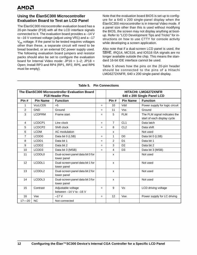
Using the ÉlanSC300 Microcontroller Evaluation Board to Test an LCD PanelThe ÉlanSC300 microcontroller evaluation board has a20-pin header (P18) with all the LCD interface signalsconnected to it. The evaluation board provides a –14 Vto –16 V contrast voltage (adjust using VR1) and a –17Vee voltage. If the panel to be tested requires voltagesother than these, a separate circuit will need to bebread boarded, or an external DC power supply used.The following evaluation board jumpers and resistorpacks should also be set to configure the evaluationboard for Internal Video mode: JP16 = 1–2; JP18 =Open; Install RP3 and RP4 (RP1, RP2, RP5, and RP6must be empty).
Note that the evaluation board BIOS is set up to config-ure for a 640 x 200 single-panel display when theÉlanSC300 microcontroller is in Internal Video mode. Ifa panel size other than this is used without modifyingthe BIOS, the screen may not display anything at boot-up. Refer to "LCD Development Tips and Tricks" for in-structions on how to use CTTY for console activitywhile developing a screen application.
Also note that if a dual-screen LCD panel is used, theSBHE, IRQ14, MCS16, and IOS16 ISA signals are nolonger available outside the chip. This means the stan-dard 16-bit IDE interface cannot be used.
Table 5 shows how the pins on the 20-pin headershould be connected to the pins of a Hi tachiLMG6272XNFR, 640 x 200 single-panel display.
Table 5. Pin Connections
The ÉlanSC300 Microcontroller Evaluation BoardP18 Header Pins
HITACHI: LMG6272XNFR640 x 200 Single Panel LCD
Pin # Pin Name Function Pin # Pin Name Function1 VccLCD5 +5 = 10 Vdd Power supply for logic circuit
2 GND Ground = 11 Vss Ground
3 LCDFRM Frame start = 5 FLM The FLM signal indicates the start of each display cycle
4 LCDCP1 Line clock = 7 CL1 Data latch
5 LCDCP2 Shift clock = 8 CL2 Data shift
6 LCDM AC modulation x Not used
7 LCDD0 Data bit 0 (LSB) = 1 D0 Data bit 0 (LSB)
8 LCDD1 Data bit 1 = 2 D1 Data bit 1
9 LCDD2 Data bit 2 = 3 D2 Data bit 2
10 LCDD3 Data bit 3 (MSB) = 4 D3 Data bit 3 (MSB)
11 LCDDL0 Dual-screen panel data bit 0 for lower panel
x Not used
12 LCDDL1 Dual-screen panel data bit 1 for lower panel
x Not used
13 LCDDL2 Dual-screen panel data bit 2 for lower panel
x Not used
14 LCDDL3 Dual-screen panel data bit 3 for lower panel
x Not used
15 Contrast Adjustable voltage between –14 V to –16 V
= 9 Vo LCD driving voltage
16 Vee –17 V = 12 Vee Power supply for LC driving
17—20 NC Not connected
12 Configuring the Élan™SC300 Device’s Internal CGA Controller for a Specific LCD Panel
LCD DEVELOPMENT TIPS & TRICKSUse CTTY for Console I/O
When using an LCD as the console device under DOS,there may be problems debugging the LCD becauseDOS will also be attempting to write to the LCD throughthe BIOS. A way around this is by diverting the DOSconsole I/O through the serial port. This allows use ofdebug or other application programs to access theÉlanSC300 microcontroller’s registers and view the re-sults on the LCD display. The following steps are rec-ommended:
1 Connect a null modem cable between COM1 on theÉlanSC300 microcontroller and a PC running PRO-COMM or other terminal program. (A lap link serialcable is a null modem cable).
2. On the PC running PROCOMM, set up for a directconnect to the serial port, running 9600 baud, 8data, 1 stop bit, and no parity. Set it up for a terminaltype of either TTY or ANSI-BBS.
3. On the ÉlanSC300 microcontroller system, bootDOS and have the following commands in the autoexec.bat file:
– mode com1 9600,n,8,1
– ctty com1
4. After the system boots, the DOS prompt will be vis-ible on the PC running PROCOMM.
5. Executing programs that use the console I/O suchas debug should be possible.
6. Programs that talk directly to video memory will dis-play the output on the ÉlanSC300 microcontroller
system, but the keyboard input will come from thePC running PROCOMM.
7. Below are two things to keep in mind:
– To debug an LCD, the ÉlanSC300 microcontrol-ler evaluation board should be configured for In-ternal Video mode
– If using Phoenix BIOS, the BIOS will lock theVideo Index registers. Remember to unlockthem by reading Video Index 12h. The BIOS willalso lock the upper 16K of display memory,which is used for font storage in Text mode. Thiscan be unlocked by clearing bit 3 of Video Index20h.
The BIOS May Also Be Updating the Screen
If using the ÉlanSC300 microcontroller evaluationboard with an LCD standalone, (i.e., not option 1above) and booting to DOS, note that the BIOS is ac-cessing the Video registers every time it is called to up-date the screen (i.e., typing in debug or from the DOSprompt). If trying to use debug or other programs tomodify the Video registers, be aware that they may bemodified by the BIOS as well, specifically Ports 3D8hand 3D9h.
Using Standard CGA or HGA Drivers on a Nonstandard Display Size
It is possible to use standard CGA or HGA drivers on anonstandard-sized screen. The method is to programthe ÉlanSC300 microcontroller with values for the LCDwidth that match those that the driver expects. TheLCD height can be set to the actual LCD height. Thiswill cause the video SRAM to be organized as the stan-dard driver is expecting. The LCD panel will be display-ing the upper left of a virtual screen.
Trademarks
Copyright © 1997 Advanced Micro Devices, Inc. All rights reserved.
AMD, the AMD logo, combinations thereof, and Élan are trademarks of Advanced Micro Devices, Inc.
Product names used in this publication are for identification purposes only and may be trademarks of their respective companies.
Configuring the Élan™SC300 Device’s Internal CGA Controller for a Specific LCD Panel 13