Embed Size (px)
Citation preview
Concevoir et produire des semiconducteurs en Europe: une Utopie ?
Let’s have a look…
Gérard MATHERON
MIDIS MINATEC24 avril 2009
1 – Advanced Wafer ManufacturingChallenges
3Midis Minatec – 24 april 2009 _GM
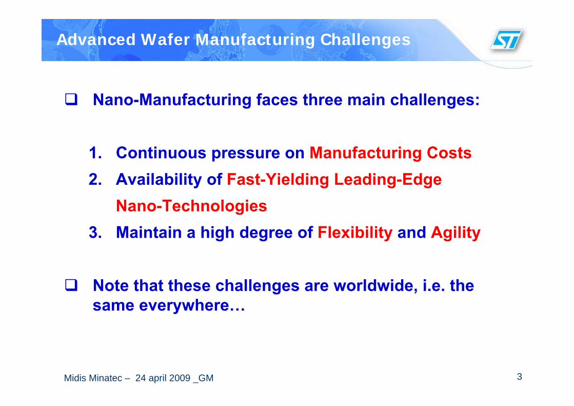
Advanced Wafer Manufacturing Challenges
Nano-Manufacturing faces three main challenges:
1. Continuous pressure on Manufacturing Costs2. Availability of Fast-Yielding Leading-Edge
Nano-Technologies3. Maintain a high degree of Flexibility and Agility
Note that these challenges are worldwide, i.e. the same everywhere…
4Midis Minatec – 24 april 2009 _GM
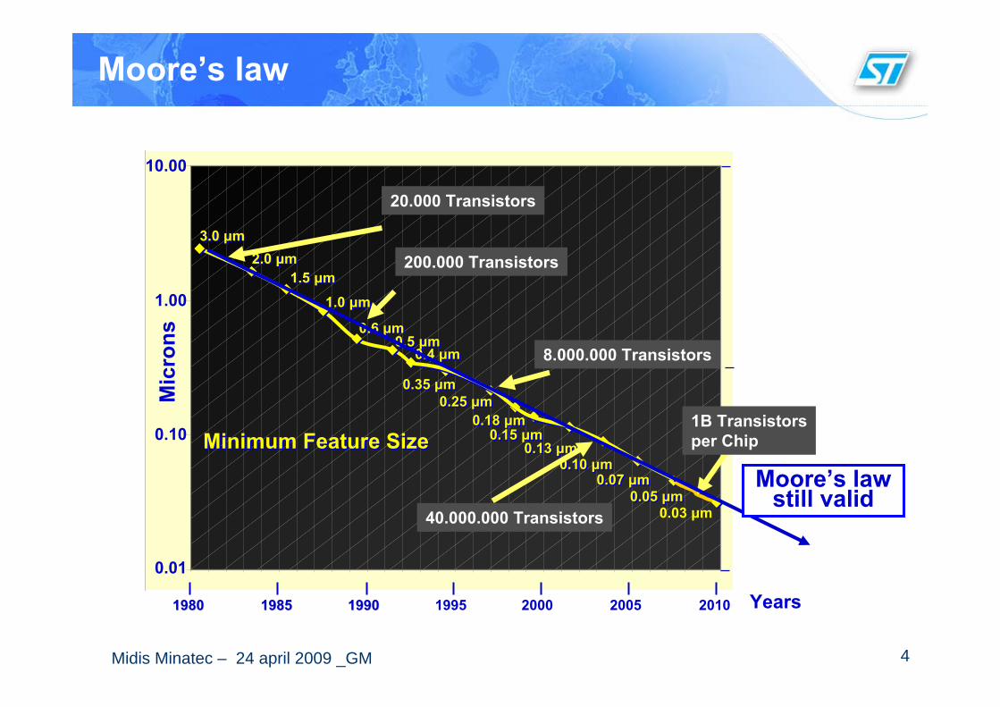
Moore’s law
0.01
0.10
1.00
10.00
J D D D D D D D D D D D D D D D D D D D D D D D D D D D D D D
19801980 19851985 19901990 1995 2000 2005 2010
Mic
rons
0.01
0.10
1.00
10.00
Years
0.15 μm0.15 μm0.18 μm0.18 μm
0.13 μm0.13 μm0.10 μm0.10 μm
0.07 μm0.07 μm0.05 μm0.05 μm
0.35 μm0.35 μm0.25 μm0.25 μm
3.0 μm3.0 μm2.0 μm2.0 μm
1.5 μm1.5 μm
1.0 μm1.0 μm
0.6 μm0.6 μm0.5 μm0.5 μm
0.4 μm0.4 μm
0.03 μm
Minimum Feature SizeMinimum Feature Size
20.000 Transistors
200.000 Transistors
8.000.000 Transistors
40.000.000 Transistors
Moore’s lawstill valid
1B Transistorsper Chip

5Midis Minatec – 24 april 2009 _GM
1 Mégabit Silicon memory
Integration doubling every 18 months enables a dramatic drop in prices per function
Moore’ s law Economic Impact

6Midis Minatec – 24 april 2009 _GM
1. Continuous pressure on Manufacturing Costs1. Continuous pressure on Manufacturing Costs
Advanced Wafer Manufacturing Challenges (1)
ASP decrease:Typically -10% per year
CostCost remains the main competitive differentiatorin Advanced Manufacturing
$0
$1 000
$2 000
$3 000
$4 000
$5 000
$6 000
$7 000
$8 000
Q1-
05
Q2-
05
Q3-
05
Q4-
05
Q1-
06
Q2-
06
Q3-
06
Q4-
06
Q1-
07
Q2-
07
Q3-
07
Q4-
07
Q1-
08
Q2-
08
Q3-
08
Q4-
08
0.25µ, Metal - 05
0.18µ, Metal - 06
0.13µ, Metal - 06
130nm, Metal - 06
90nm, Metal - 06
65nm, Metal - 08
300mm
200mm
Foundry Wafer Pricing Trend 2005-2008
Source: Gartner Dataquest
7Midis Minatec – 24 april 2009 _GM
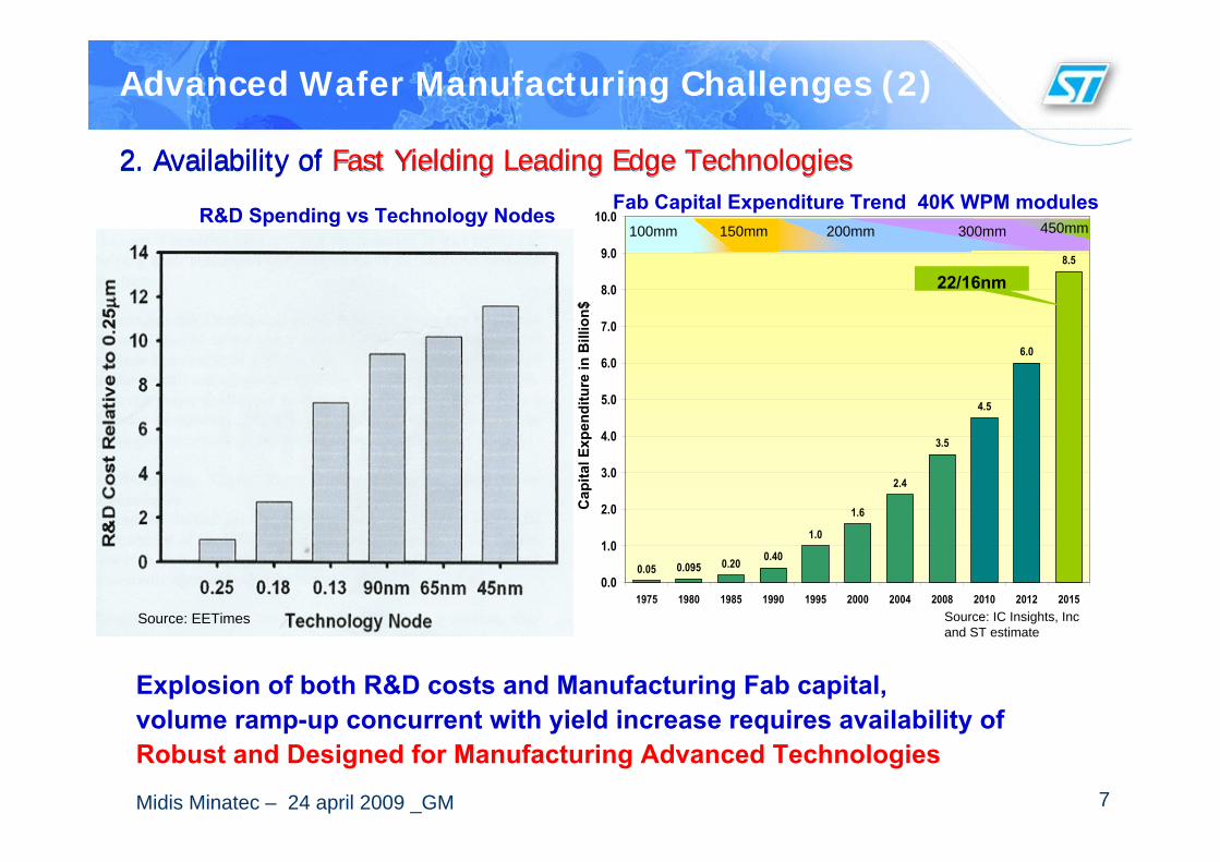
Advanced Wafer Manufacturing Challenges (2)
Explosion of both R&D costs and Manufacturing Fab capital, volume ramp-up concurrent with yield increase requires availability ofRobust and Designed for Manufacturing Advanced Technologies
2. Availability of Fast Yielding Leading Edge Technologies2. Availability of Fast Yielding Leading Edge TechnologiesFast Yielding Leading Edge Technologies
1.0
1.6
2.4
3.5
4.5
6.0
8.5
0.400.200.05 0.0950.0
1.0
2.0
3.0
4.0
5.0
6.0
7.0
8.0
9.0
10.0
1975 1980 1985 1990 1995 2000 2004 2008 2010 2012 2015
Source: EETimes
R&D Spending vs Technology Nodes
Cap
ital E
xpen
ditu
re in
Bill
ion$
22/16nm
Source: IC Insights, Incand ST estimate
Fab Capital Expenditure Trend 40K WPM modules100mm 150mm 200mm 300mm 450mm
8Midis Minatec – 24 april 2009 _GM
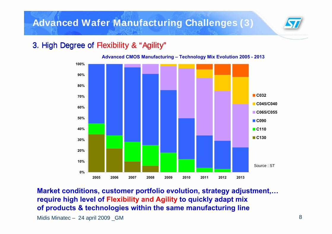
3. High Degree of Flexibility & “Agility”3. High Degree of Flexibility & Flexibility & ““AgilityAgility””
Advanced Wafer Manufacturing Challenges (3)
Market conditions, customer portfolio evolution, strategy adjustment,…require high level of Flexibility and Agility to quickly adapt mix of products & technologies within the same manufacturing line
Advanced CMOS Manufacturing – Technology Mix Evolution 2005 - 2013
0%
10%
20%
30%
40%
50%
60%
70%
80%
90%
100%
2005 2006 2007 2008 2009 2010 2011 2012 2013
C032
C045/C040
C065/C055
C090
C110
C130
Source : ST
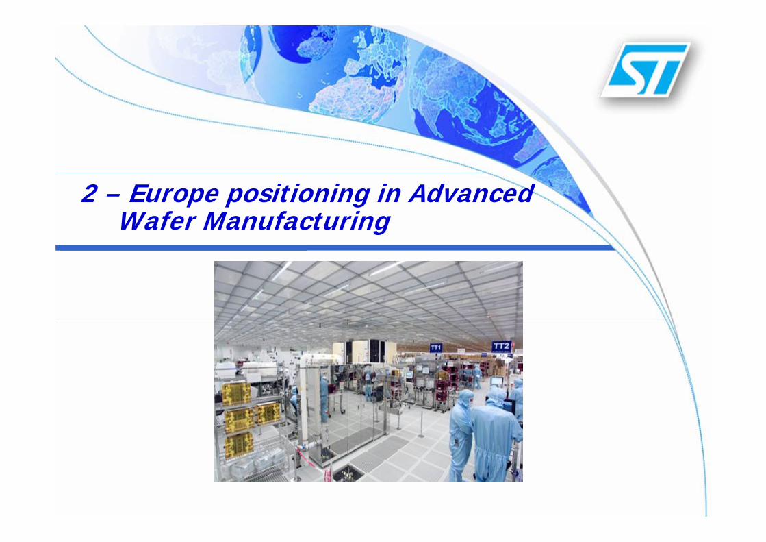
2 – Europe positioning in Advanced Wafer Manufacturing

10Midis Minatec – 24 april 2009 _GM
Threats on Advanced Wafer Manufacturing in Europe
Costs– Currencies (€/$ exchange rate )– Labor cost– Excessive external equipment maintenance – Economical environment (taxes, incentives…) despite
some local improvements (eg Nano2012)
Dimension of Scale– Too many small size Fabs, mainly for historical reasons
Cultural– Weak education in Manufacturing Sciences and Industrial
Engineering
Constraints– Labor policies, limited flexibility in employment conditions– Legislative environment on ESH (eg REACH)
11Midis Minatec – 24 april 2009 _GM
Opportunities for Advanced Wafer Manufacturing in Europe
Leadership in R&D– World-Class industrial Laboratories & Institutes (LETI…)– High count of PhDs in process development & design– High level of R&D efforts from SC companies– Significant funding support from National & EU Authorities
Clustering– Regional Excellence Centers in R&D, Design & Manufacturing
with proximity of Suppliers and Application Centers
Market– European leadership in several strategic markets where IC’s are
providing innovation (Medical, Power, Automotive, Wireless and Environment)
Human Resources– Undisputed expertise, stability & engagement
12Midis Minatec – 24 april 2009 _GM
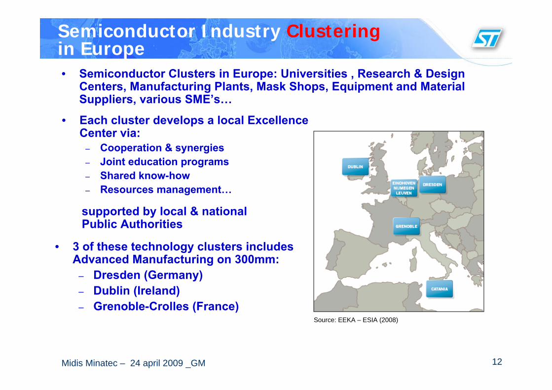
Semiconductor Industry Clusteringin Europe• Semiconductor Clusters in Europe: Universities , Research & Design
Centers, Manufacturing Plants, Mask Shops, Equipment and Material Suppliers, various SME’s…
supported by local & national Public Authorities
• 3 of these technology clusters includes Advanced Manufacturing on 300mm:
– Dresden (Germany)– Dublin (Ireland)– Grenoble-Crolles (France)
• Each cluster develops a local Excellence Center via:
– Cooperation & synergies– Joint education programs– Shared know-how– Resources management…
Source: EEKA – ESIA (2008)

13Midis Minatec – 24 april 2009 _GM
European Semiconductor Industry fueled by European Market Leaderships
European Leadership in key industry sectors helps semiconductorcompanies to keep leading edge as well, due to stronger than everprocess-system design integration
Electronic systems OEM rankings
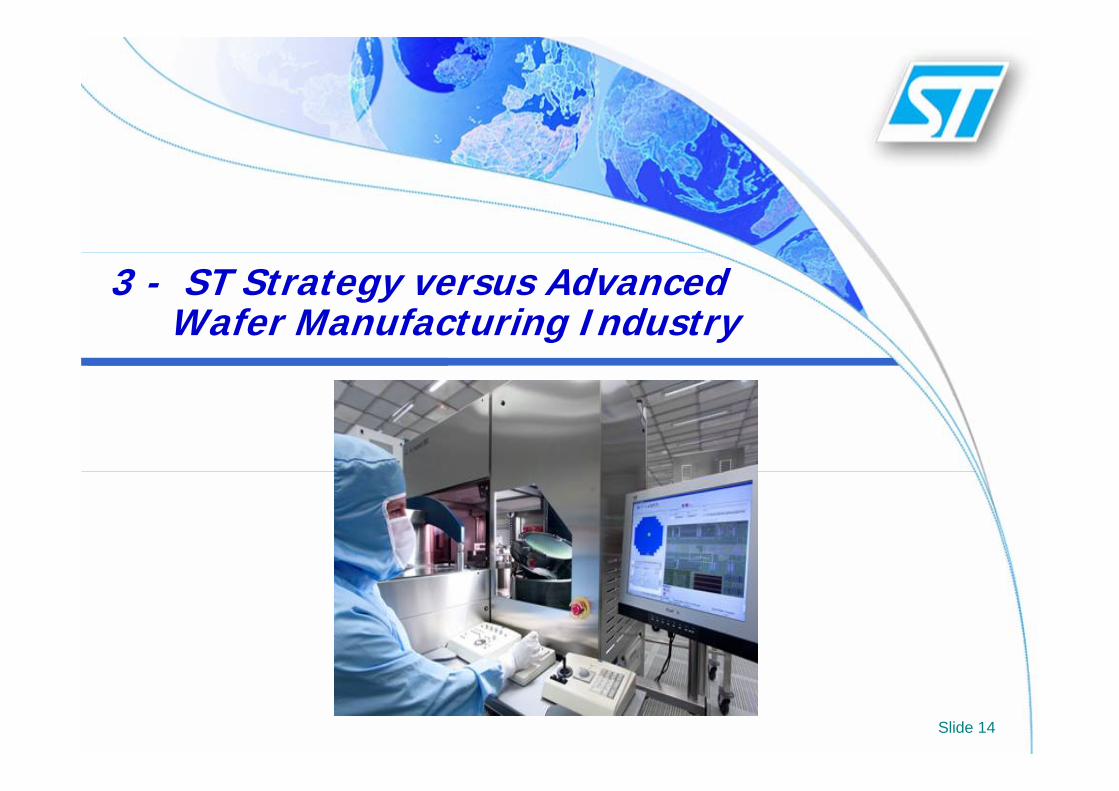
3 - ST Strategy versus AdvancedWafer Manufacturing Industry
Slide 14
15Midis Minatec – 24 april 2009 _GM
Technology Roadmap: Strategic Guidelines
Technology sourcing:
– Advanced core CMOS : through IBM consortium (32nm and below)
– Derivative & Proprietary processes : internally developed
Technology Leadership in Smart Power, CMOS Derivatives, Analog and Discretes, MEMS
Development of “More than Moore” technologies (power, analog/RF, sensors, MEMS…) driven by applications
Innovation and Differentiation via new developments and partnerships:
– New silicon technologies (bio-technology & healthcare, fuel cell,…)
– Post-silicon technologies (nano-technologies & printed electronics,…)
16Midis Minatec – 24 april 2009 _GM
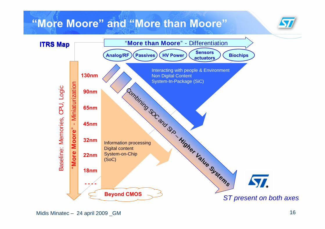
“More Moore” and “More than Moore”
ITRS MapITRS Map “More than Moore” - Differentiation
“Mor
e M
oore
”-
Min
iatu
rizat
ion
130nm
90nm
65nm
45nm
32nm
22nm
18nm
- - - -
Analog/RF Passives HV Power Sensorsactuators Biochips
Base
line:
Mem
orie
s, C
PU, L
ogic Combining SOC and SIP – Higher Value System
s
Interacting with people & EnvironmentNon Digital ContentSystem-In-Package (SiC)
Information processingDigital contentSystem-on-Chip(SoC)
Beyond CMOS ST present on both axes
17Midis Minatec – 24 april 2009 _GM
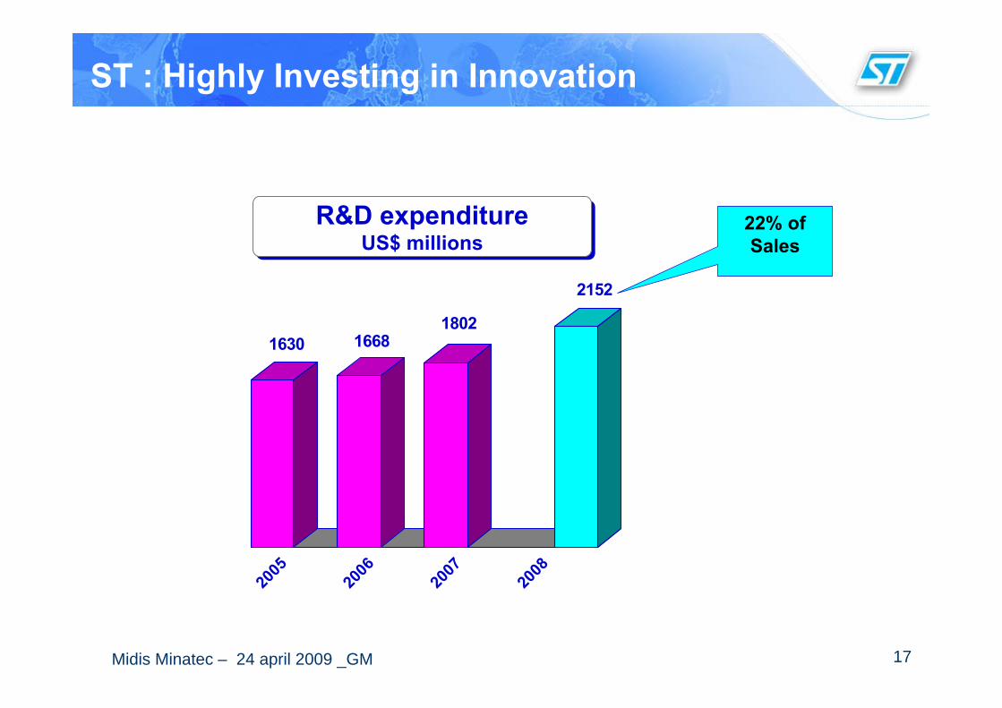
ST : Highly Investing in Innovation
R&D expenditureUS$ millions
R&D expenditureUS$ millions
1630 16681802
2152
2005
2006
2007
2008
22% of Sales
18Midis Minatec – 24 april 2009 _GM
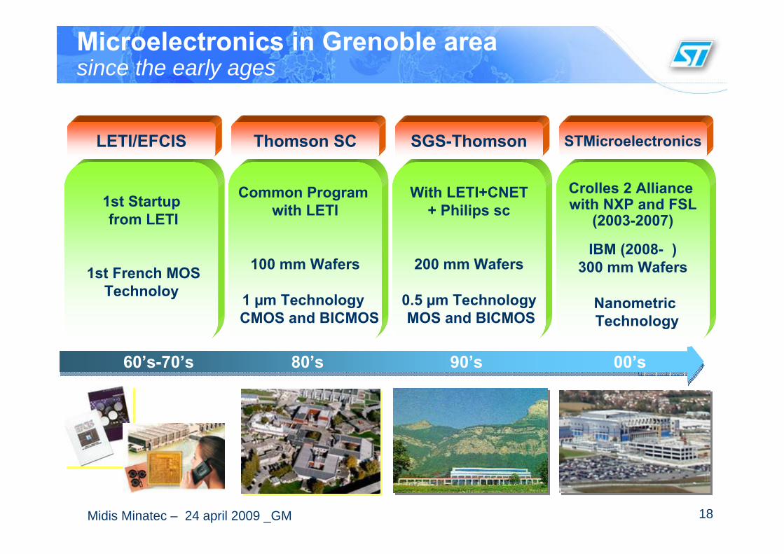
Microelectronics in Grenoble area since the early ages
60’s-70’s 80’s 90’s 00’s
1st Startupfrom LETI
1st French MOSTechnoloy
LETI/EFCIS
Common Program with LETI
100 mm Wafers
1 µm Technology CMOS and BICMOS
Thomson SC
With LETI+CNET+ Philips sc
200 mm Wafers
0.5 µm TechnologyMOS and BICMOS
SGS-Thomson
Crolles 2 Alliance with NXP and FSL
(2003-2007)
IBM (2008- )300 mm Wafers
NanometricTechnology
STMicroelectronics

19Midis Minatec – 24 april 2009 _GM
ST Crolles site
Crolles200Crolles200 Crolles300Crolles300
20Midis Minatec – 24 april 2009 _GM
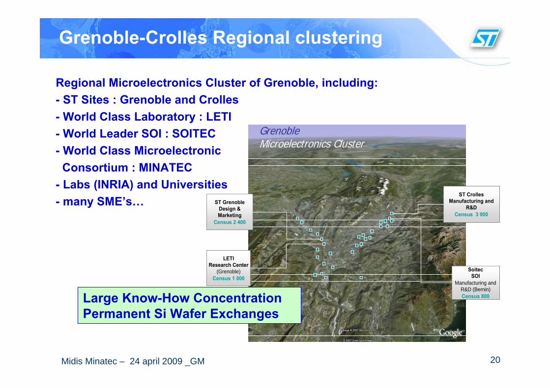
Grenoble-Crolles Regional clustering
Regional Microelectronics Cluster of Grenoble, including:- ST Sites : Grenoble and Crolles - World Class Laboratory : LETI - World Leader SOI : SOITEC - World Class MicroelectronicConsortium : MINATEC
- Labs (INRIA) and Universities- many SME’s…
GrenobleMicroelectronics Cluster
ST Grenoble Design & Marketing
Census 2 400
LETIResearch Center
(Grenoble)Census 1 000
ST Grenoble Design & Marketing
Census 2 400
LETIResearch Center
(Grenoble)Census 1 000
ST CrollesManufacturing and
R&DCensus 3 900
SoitecSOI
Manufacturing and R&D (Bernin)Census 800
ST CrollesManufacturing and
R&DCensus 3 900
ST CrollesManufacturing and
R&DCensus 3 900
SoitecSOI
Manufacturing and R&D (Bernin)Census 800
SoitecSOI
Manufacturing and R&D (Bernin)Census 800Large Know-How Concentration
Permanent Si Wafer Exchanges
21Midis Minatec – 24 april 2009 _GM
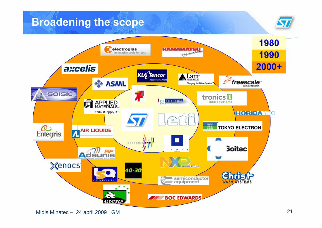
Broadening the scope
2000+19901980

22Midis Minatec – 24 april 2009 _GM
ST Crolles Impact on Jobs creation
+ Indirect 8000
+ Direct 4000
ST Crolles4074
Total Rhône-Alpes ~ 16000 p
plus 9000 p in France
Total Rhône-Alpes ~ 16000 p
plus 9000 p in France
23Midis Minatec – 24 april 2009 _GM
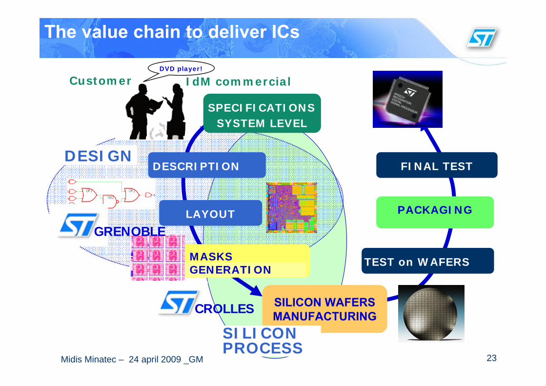
DVD player!
Customer
DESIGN
SPECIFICATIONSSYSTEM LEVEL
DESCRIPTION
LAYOUT
SILICON WAFERSMANUFACTURING
TEST on WAFERS
PACKAGING
FINAL TEST
The value chain to deliver ICs
SILICON PROCESS
IdM commercial
MASKS GENERATION
CROLLES
GRENOBLE

24Midis Minatec – 24 april 2009 _GM
R&D: a Global Alliance for Core CMOS Process development
for Bulk CMOS Technology developmentInternational Silicon Development Alliance
CharteredSamsung
InfineonToshiba
FreescaleST
AMD/Foundry co
25Midis Minatec – 24 april 2009 _GM
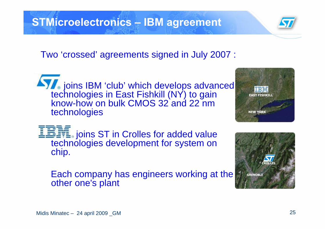
STMicroelectronics – IBM agreement
Two ‘crossed’ agreements signed in July 2007 :
joins IBM ‘club’ which develops advanced technologies in East Fishkill (NY) to gain know-how on bulk CMOS 32 and 22 nm technologies
joins ST in Crolles for added value technologies development for system on chip.
Each company has engineers working at the other one's plant
26Midis Minatec – 24 april 2009 _GM
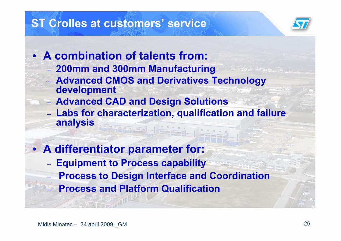
• A combination of talents from:– 200mm and 300mm Manufacturing– Advanced CMOS and Derivatives Technology
development– Advanced CAD and Design Solutions– Labs for characterization, qualification and failure
analysis
• A differentiator parameter for:– Equipment to Process capability– Process to Design Interface and Coordination– Process and Platform Qualification
ST Crolles at customers’ service
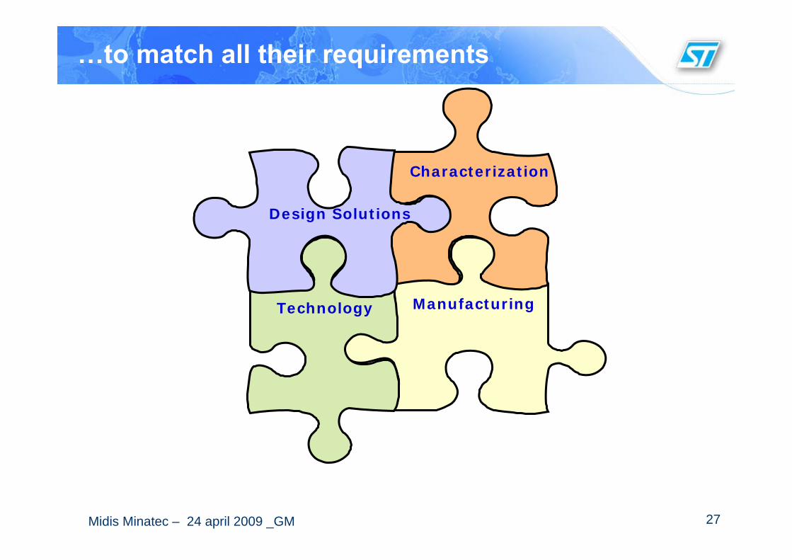
27Midis Minatec – 24 april 2009 _GM
Characterization
ManufacturingTechnology
Design Solutions
…to match all their requirements
28Midis Minatec – 24 april 2009 _GM
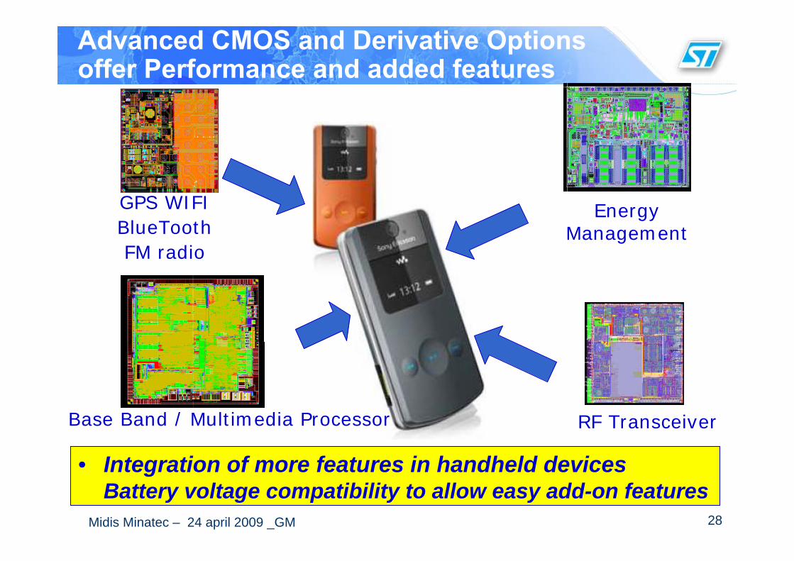
Advanced CMOS and Derivative Options offer Performance and added features
• Integration of more features in handheld devicesBattery voltage compatibility to allow easy add-on features
GPS WIFIBlueToothFM radio
Base Band / Multimedia Processor RF Transceiver
EnergyManagement
29Midis Minatec – 24 april 2009 _GM
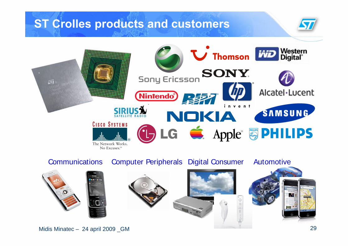
ST Crolles products and customers
Communications Computer Peripherals AutomotiveDigital Consumer
30Midis Minatec – 24 april 2009 _GM
R&D, Design, Applications, ManufacturingST clustering in Europe• Clustering of R&D, Design , Applications, and Manufacturing on the
same site provides significant advantages:
– Speed & Acceleration of the learning curve:• Close loop between various teams
• Fast Design/Silicon prototyping
• Reduce communication barriers
– Excellence Center driven by Business & Customer Application:
• All activities in convergence
• Knowledge & experience sharing
• Innovation enabler across each organization
– Efficiency:• Focus
• Synergy
• Reactivity

31Midis Minatec – 24 april 2009 _GM
9000 m2
6700 m2
1900 m2
Clean link
Facilities
Cleanroom C300
Cleanroom C200
32Midis Minatec – 24 april 2009 _GM
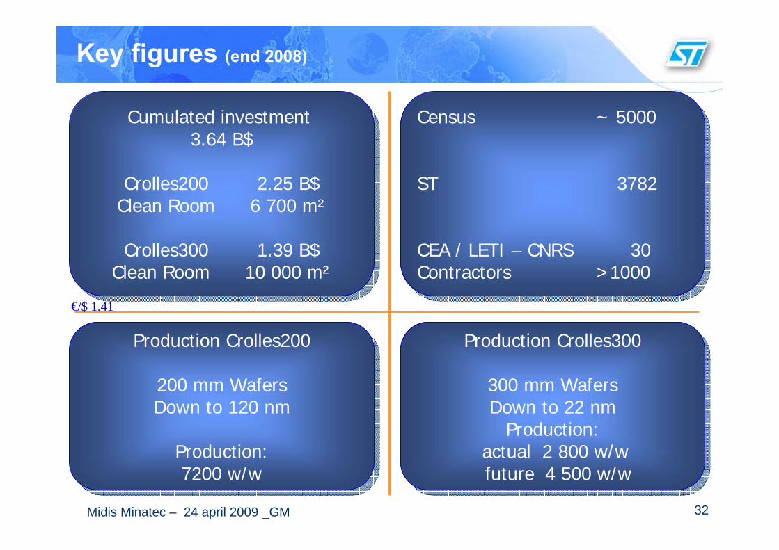
Key figures (end 2008)
Cumulated investment 3.64 B$
Crolles200 2.25 B$Clean Room 6 700 m²
Crolles300 1.39 B$Clean Room 10 000 m²
Cumulated investment 3.64 B$
Crolles200 2.25 B$Clean Room 6 700 m²
Crolles300 1.39 B$Clean Room 10 000 m²
Census ~ 5000
ST 3782
CEA / LETI – CNRS 30Contractors >1000
Census ~ 5000
ST 3782
CEA / LETI – CNRS 30Contractors >1000
Production Crolles300
300 mm WafersDown to 22 nm
Production:actual 2 800 w/wfuture 4 500 w/w
Production Crolles300
300 mm WafersDown to 22 nm
Production:actual 2 800 w/wfuture 4 500 w/w
Production Crolles200
200 mm WafersDown to 120 nm
Production:7200 w/w
Production Crolles200
200 mm WafersDown to 120 nm
Production:7200 w/w
€/$ 1.41
33Midis Minatec – 24 april 2009 _GM
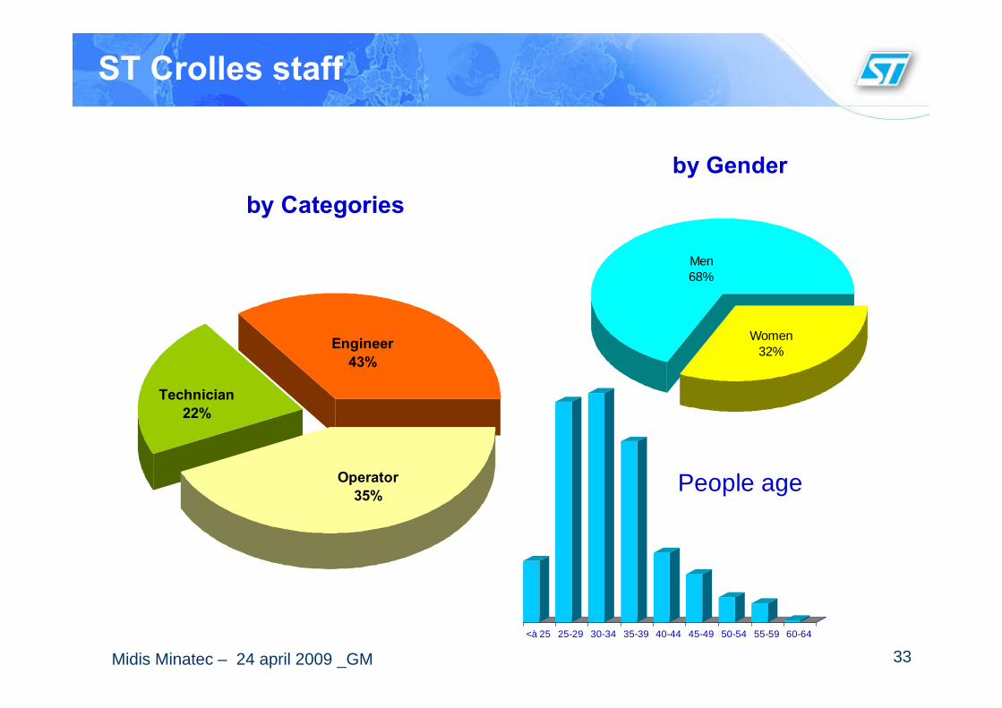
ST Crolles staff
by Categories
Engineer43%
Operator35%
Technician22%
by Gender
Women32%
Men68%
<à 25 25-29 30-34 35-39 40-44 45-49 50-54 55-59 60-64
People age
34Midis Minatec – 24 april 2009 _GM
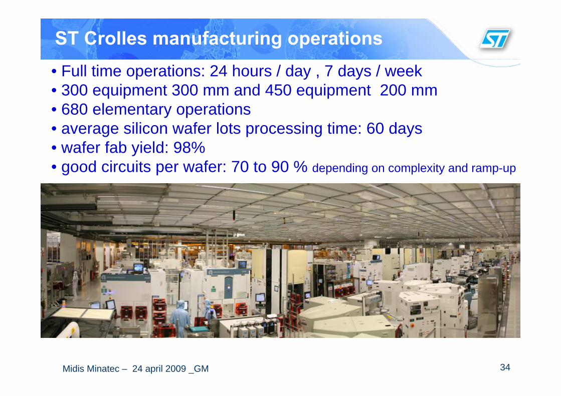
ST Crolles manufacturing operations• Full time operations: 24 hours / day , 7 days / week• 300 equipment 300 mm and 450 equipment 200 mm • 680 elementary operations• average silicon wafer lots processing time: 60 days• wafer fab yield: 98%• good circuits per wafer: 70 to 90 % depending on complexity and ramp-up
35Midis Minatec – 24 april 2009 _GM
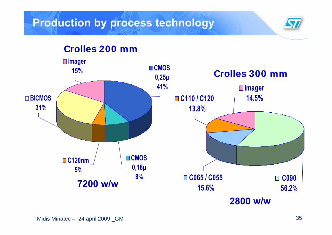
Production by process technology
C120nm5%
CMOS 0,18µ
8%
CMOS 0,25µ41%
BICMOS31%
Imager15%
Imager14.5%
C09056.2%
C065 / C05515.6%
C110 / C12013.8%
Crolles 200 mm
Crolles 300 mm
7200 w/w
2800 w/w
36Midis Minatec – 24 april 2009 _GM
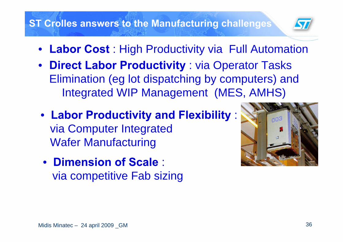
ST Crolles answers to the Manufacturing challenges
• Labor Cost : High Productivity via Full Automation• Direct Labor Productivity : via Operator Tasks
Elimination (eg lot dispatching by computers) andIntegrated WIP Management (MES, AMHS)
• Labor Productivity and Flexibility :via Computer Integrated Wafer Manufacturing
• Dimension of Scale : via competitive Fab sizing
37Midis Minatec – 24 april 2009 _GM
• ST Crolles 300mm Fab at 20 K Wafer/Month cancombine efficiently R&D and Manufacturing ofDifferentiated Technologies:– CMOS Analog / RF process– Embedded Memories (DRAM, NVM)– CMOS Imagers with Colorization line– TSV process– 3 D integration
• Benefits of R&D ‘embedded’ within Manufacturing :– Fast Silicon close loops– Fast prototyping– Fast Yield learning curve– Same tools R&D – Mfg– Concentration of Expertise (Design, Process, Manufacturing)
ST Crolles Focus on Differentiated Technologies
38Midis Minatec – 24 april 2009 _GM
Summary
• Top-class silicon process devt via local and ww alliances
• On-site Platform expertise for complex system-on chip development
• Service-oriented manufacturing
• Completed with close contacts with ST and ST- Ericsson design teams at Grenoble and many other ST and customers’ sites
NO, designing and manufacturing advancedsemiconductors in Europe is not an Utopy !It’s happening HERE and NOW