Embed Size (px)
Citation preview
Concentrator photovoltaic module architectures withcapabilities for capture and conversion of full globalsolar radiationKyu-Tae Leea,b,1, Yuan Yaoc,1, Junwen Hec,1, Brent Fisherd, Xing Shenge, Matthew Lumbf,g, Lu Xuc,Mikayla A. Andersonc, David Scheimang, Seungyong Hana,b, Yongseon Kanga,b, Abdurrahman Gumush,Rabab R. Bahabryh, Jung Woo Leea,b,i,j, Ungyu Paiki,j, Noah D. Bronsteink, A. Paul Alivisatosk,l,m,n, Matthew Meitld,Scott Burroughsd, Muhammad Mustafa Hussainh, Jeong Chul Leea,b,2, Ralph G. Nuzzoa,b,c,2, and John A. Rogersa,b,c,2
aDepartment of Materials Science and Engineering, University of Illinois at Urbana–Champaign, Urbana, IL 61801; bFrederick Seitz Materials ResearchLaboratory, University of Illinois at Urbana–Champaign, Urbana, IL 61801; cDepartment of Chemistry, University of Illinois at Urbana–Champaign, Urbana,IL 61801; dSemprius, Durham, NC 27713; eDepartment of Electronic Engineering, Tsinghua University, Beijing, China 100084; fThe George WashingtonUniversity, Washington, DC 20037; gUS Naval Research Laboratory, Washington, DC 20375; hIntegrated Nanotechnology Lab, Computer, Electrical andMathematical Sciences and Engineering Division, King Abdullah University of Science and Technology, Thuwal, Saudi Arabia; iDepartment of MaterialsScience and Engineering, Hanyang University, Seoul 133-791, Republic of Korea; jDepartment of Energy Engineering, Hanyang University, Seoul 133-791,Republic of Korea; kDepartment of Chemistry, University of California, Berkeley, CA 94720; lDepartment of Materials Science and Engineering, University ofCalifornia, Berkeley, CA 94720; mKavli Energy NanoScience Institute, University of California, Berkeley, CA 94720; and nMaterials Science Division, LawrenceBerkeley National Laboratory, Berkeley, CA 94720
Contributed by John A. Rogers, October 21, 2016 (sent for review September 7, 2016; reviewed by Yi Cui and Gary P. Wiederrecht)
Emerging classes of concentrator photovoltaic (CPV) modules reachefficiencies that are far greater than those of even the highestperformance flat-plate PV technologies, with architectures that havethe potential to provide the lowest cost of energy in locations withhigh direct normal irradiance (DNI). A disadvantage is their inabilityto effectively use diffuse sunlight, thereby constraining widespreadgeographic deployment and limiting performance even under themost favorable DNI conditions. This study introduces a moduledesign that integrates capabilities in flat-plate PV directly with themost sophisticated CPV technologies, for capture of both direct anddiffuse sunlight, thereby achieving efficiency in PV conversion of theglobal solar radiation. Specific examples of this scheme exploit com-modity silicon (Si) cells integrated with two different CPV moduledesigns, where they capture light that is not efficiently directed bythe concentrator optics onto large-scale arrays of miniature multi-junction (MJ) solar cells that use advanced III–V semiconductor tech-nologies. In this CPV+ scheme (“+” denotes the addition of diffusecollector), the Si and MJ cells operate independently on indirect anddirect solar radiation, respectively. On-sun experimental studies ofCPV+ modules at latitudes of 35.9886° N (Durham, NC), 40.1125° N(Bondville, IL), and 38.9072° N (Washington, DC) show improve-ments in absolute module efficiencies of between 1.02% and8.45% over values obtained using otherwise similar CPV modules,depending on weather conditions. These concepts have the poten-tial to expand the geographic reach and improve the cost-effective-ness of the highest efficiency forms of PV power generation.
photovoltaics | multijunction solar cells | concentration optics | diffuse lightcapture
The levelized cost of electricity (LCOE) is a primary metricthat defines the economic competitiveness of photovoltaic
(PV) approaches to electrical power generation (1). As theperformance of the highest efficiency single-junction flat-platePV modules begins to reach theoretical limits, research towardcost reductions in such technologies shifts from performance totopics related to materials utilization and manufacturing (2–5).By contrast, the efficiencies of multijunction (MJ) solar cellsbased on III–V compound semiconductors continue to improvesteadily, at a rate of ∼1% per year over the last 15 y, due largelyto progress in epitaxial growth processes, mechanical stackingtechniques, and microassembly methods for adding junctionsthat further maximize light absorption and minimize carrierthermalization losses (6–20). Record MJ cell efficiencies nowapproach ∼46.0%, with realistic pathways to the 50% milestone
(5). For economic deployment, however, the sophistication andassociated costs of these cells demand the use of lenses, curvedmirrors, or other forms of optics in conjunction with a me-chanical tracker to geometrically concentrate incident directsunlight in a manner that maximizes cell utilization (21, 22). Onecommercial technology of interest uses a two-stage optical con-centrating system that consists of an array of aspheric primarylenses and ball lenses interfaced to arrays of ultrathin, triple-junction (3J) III–V cells with submillimeter lateral dimensionsformed by lithographic processes and epitaxial liftoff (23–25).
Significance
Concentrator photovoltaic (CPV) systems, wherein light focusesonto multijunction solar cells, offer the highest efficiencies inconverting sunlight to electricity. The performance is in-trinsically limited, however, by an inability to capture diffuseillumination, due to narrow acceptance angles of the concen-trator optics. Here we demonstrate concepts where flat-platesolar cells mount onto the backplanes of the most sophisti-cated CPV modules to yield an additive contribution to theoverall output. Outdoor testing results with two different hy-brid module designs demonstrate absolute gains in averagedaily efficiencies of between 1.02% and 8.45% depending onweather conditions. The findings suggest pathways to signifi-cant improvements in the efficiencies, with economics thatcould potentially expand their deployment to a wide range ofgeographic locations.
Author contributions: K.-T.L., Y.Y., J.H., X.S., J.C.L., R.G.N., and J.A.R. designed research;K.-T.L., Y.Y., J.H., B.F., M.L., L.X., M.A.A., D.S., S.H., Y.K., A.G., R.R.B., J.W.L., U.P., N.D.B.,A.P.A., M.M., S.B., M.M.H., J.C.L., R.G.N., and J.A.R. performed research; K.-T.L., Y.Y., J.H.,B.F., J.C.L., R.G.N., and J.A.R. analyzed data; and K.-T.L., Y.Y., J.H., R.G.N., and J.A.R. wrotethe paper.
Reviewers: Y.C., Stanford University; and G.P.W., Argonne National Laboratory.
Conflict of interest statement: B.F., M.M., S.B., R.G.N., and J.A.R. are affiliated with Sem-prius, a company that is pursuing commercial, grid-scale photovoltaic technologies thatform a starting point for the advanced embodiments described and studied in this paper.Semprius does not, however, have any active programs toward commercialization ofthese embodiments. The authors declare that B.F., M.M., S.B., R.G.N., and J.A.R. areinvolved in Semprius, a company that has commercialized certain classes of concentratorphotovoltaic technologies.1K.-T.L., Y.Y., and J.H. contributed equally to this work.2To whom correspondencemay be addressed. Email: [email protected], [email protected],or [email protected].
This article contains supporting information online at www.pnas.org/lookup/suppl/doi:10.1073/pnas.1617391113/-/DCSupplemental.
E8210–E8218 | PNAS | Published online December 5, 2016 www.pnas.org/cgi/doi/10.1073/pnas.1617391113
Here, transfer printing enables high-volume manufacturing andassembly of cells with these small dimensions (26–32). The balllenses, as secondary optics, improve manufacturing tolerances,produce uniform irradiation profiles on the cells by correctingfor chromatic aberration, and expand the acceptance angle tonearly ±1° even at concentration ratios of >1,000 (22). Thecompact sizes and weights of the resulting high-concentrator PV(HCPV) modules facilitate transport and installation and enableuse of mechanical trackers with cost-effective designs. Productionsystems exhibit efficiencies of 35.5% at concentration ratios>1,000× under Concentrator Standard Test Conditions (CSTC).Terrestrial use of these, and other, types of HCPV technologies
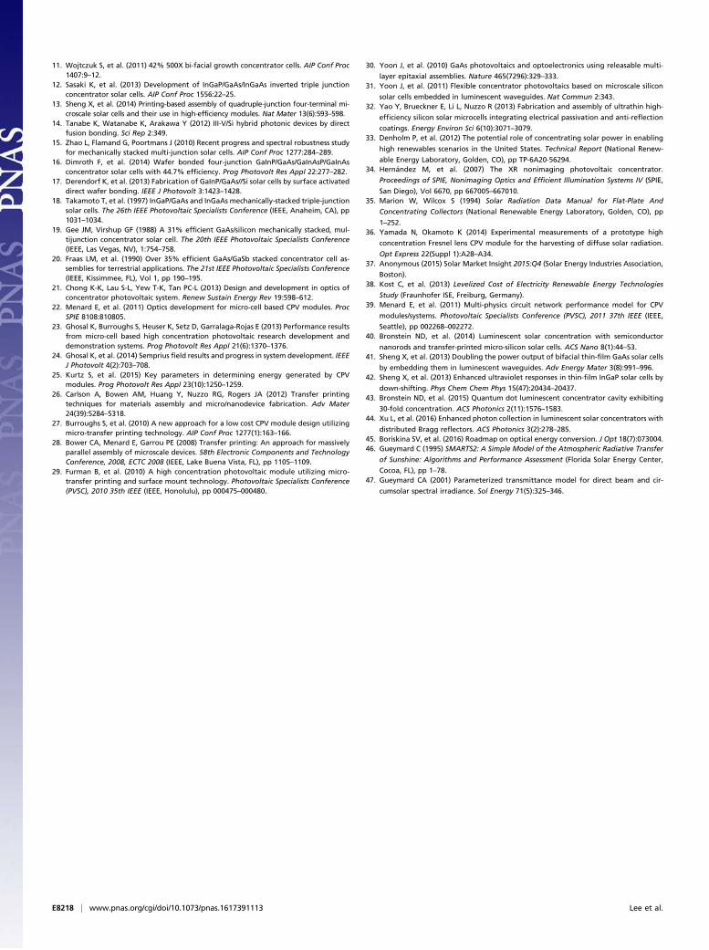
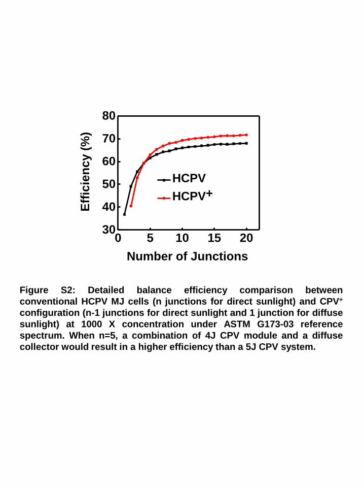
is most economically attractive in geographic locations with highlevels of direct normal irradiance (DNI) (e.g., >6 kWh/m2/d).Typical sites in the United States include California, Arizona, andNew Mexico (33). Limitations follow from the inability to usenondirect (i.e., diffuse) sunlight due to narrow acceptance anglesof the concentrating optics, as dictated by the étendue conser-vation law (e.g., with a passive concentrator operating at a con-centration ratio of 1,000, the acceptance angle is theoreticallylimited to 1.8°) (34). Even in locations such as Tucson, AZ (17%diffuse) and Daggett, CA (20% diffuse) that have exceptionallyhigh DNI, the enhancements associated with capture and con-version of diffuse illumination can be significant. In other loca-tions such as San Francisco (29.6% diffuse) and Portland, OR(39.2% diffuse), operation under diffuse light becomes even moreessential to the economics. Engineering solutions to this chal-lenge have the potential to expand the application of con-centrator systems to areas where they have previously beenuncompetitive (35, 36). SI Appendix, Fig. S1 presents estimatesfor the absolute increases in efficiency that can be expected inthese locations (35). As a perspective on the significance, cal-culations using detailed balance predict that the efficiency en-hancements enabled by adding a diffuse collector with anoptimized bandgap can exceed those provided by a replacementof 4J cells with 5J alternatives under standard AM 1.5G spec-trum (10% diffuse) (SI Appendix, Fig. S2). The ability to usediffuse sunlight also makes CPV less susceptible to soiling issues,as the scattered (by soiling) direct beam rays, which are notconcentrated onto the high-efficiency MJ cells (ranges from 2%to 10% depending on locations and weather conditions; SI Ap-pendix, Fig. S3), can be captured by the diffuse collectors. As afirst attempt to capture diffuse light, a recent report introduceda prototype minimodule device built on a conventional CPVplatform through the addition of silicon (Si) cells with arrays ofcircular holes to allow passage of focused light onto underlyingMJ cells (36). This demonstration, however, involved concen-tration ratios (<500×) that are too low to be economically viable,and standard cells and single-stage optical components that posesignificant challenges in thermal management, efficient/accuratetracking, and manufacturing tolerances. The two advanced CPVtechnologies examined here avoid these and other key limita-tions, thereby providing the basis for a realistic, competitiveapproach to PV power generation.The work reported here examines advanced modes of imple-
mentation and detailed analysis in the context of the mostadvanced commercially available HCPV module, designed forutility-scale power generation in solar farms, as described above,and of a previously unpublished, ultrathin design, configured foruse on rooftops and in space applications. Specifically, the fol-lowing results experimentally and theoretically examine schemesthat incorporate capabilities in diffuse light capture into thesetwo types of module architectures. The version that uses theHCPV technology outlined above exploits laser-cut strips ofconventional Si cells, without machined holes, mounted in aform-fitting manner onto the module backplanes. These systemsoffer economically viable concentration ratios, (>1,000×) withadvanced microscale cells for improved thermal management,
and dual-stage optics for efficient/accurate tracking andmanufacturing tolerances. (In the following, we refer to this modulearchitecture as HCPV+-DS, where "+" refers to capabilities in dif-fuse light capture and DS to the dual-stage optics). The other ar-chitecture employs a compact design optimized for diffuse lightcapture, where MJ cells on a transparent substrate stack directlyonto an unmodified commodity Si cell. These components couple toan overlying thin plano-convex (PCX) lens array, enabling an ex-ceptionally low-profile module (<5 mm in total thickness) suitablefor deployment in space-restricted areas (e.g., rooftops) or in ap-plications where weight is a primary concern (e.g., portable systems,or space applications). (In the following, we refer to this modulearchitecture as CPV+-LP, where the LP refers to low-profile opticsand the absence of H refers to the modest concentration ratios.)Compared with conventional designs, the CPV+-LP architectureoffers additional cost advantages because its ultracompact sizeand lightweight design significantly reduce both installation/trans-portation expenses and the steel required for the mechanical tracker.The economic rationale for both of these designs rests on the
fact that ∼80% of the cost of energy from flat-plate PV tech-nology comes from non–cell-related balance-of-module andbalance-of-system (BOS) cost associated with land, transport,installation, and maintenance (i.e., the turnkey cost in Q4-2015of a utility-scale plant with tracking is $1.54/Wdc and the cost ofthe Si cells is $0.33/W) (2, 37). As a result, the addition of the Sicells to an otherwise well-designed CPV platform can representan incremental cost, justified by the improved performance andconsistency of output. Specifically, at current market prices, thecost of the Si cells (i.e., without enclosure, package, inverter,BOS cost, etc.) in a conventional flat-plate PV system corre-sponds to ∼15% of the LCOE for that system (1, 37). Assumingthat the CPV technology used in this work is economicallycompetitive with Si flat plate in regions of moderate to high DNI(38), the cost for adding Si cells to CPV is approximately only7.5% of the LCOE, because the output per unit area of a Simodule is roughly one-half that for a corresponding CPV mod-ule. The economic case for the CPV+ concept follows fromcomparison of the marginal cost of adding the Si (7.5%) to thebenefit in terms of additional energy generated. Experimentalresults reported here suggest that the addition of Si cells to CPVmodules increases the overall energy production by roughly 10%even in regions of the United States with the most abundantdirect solar radiation resources (diffuse component ∼20%,assuming the Si cell efficiency is ∼50% of the CPV module),thereby supporting the potential for an overall reduction in theLCOE. Current trends in reductions in the costs of Si cells andincreases in the efficiencies of III–V cells could make such CPV+
architectures even more attractive in the future.The CPV+ concept also yields significant increases in power
per unit area, relevant for all applications: from deployment inregions of high DNI where ∼20% of the solar resource is in theform of diffuse light, to markets with constrained rooftop space,and to geographic domains with modest DNI. Outdoor fieldtesting of HCPV+-DS and CPV+-LP modules, as described indetail subsequently, shows absolute increases in efficiencies ofbetween 1.02% and 8.45% at a latitude of 35.9886° N (Durham,NC), 1.97–6.06% at a latitude of 40.1125° N (Bondville, IL), and5.20% at a latitude of 38.9072° N (Washington, DC) in typicalweather conditions in the spring, summer, and fall months. Anadditional advantage of these systems is that the large numbersof cells in the platforms provide flexibility in matching theirelectrical outputs to yield standardized two-terminal moduleinterfaces (39).
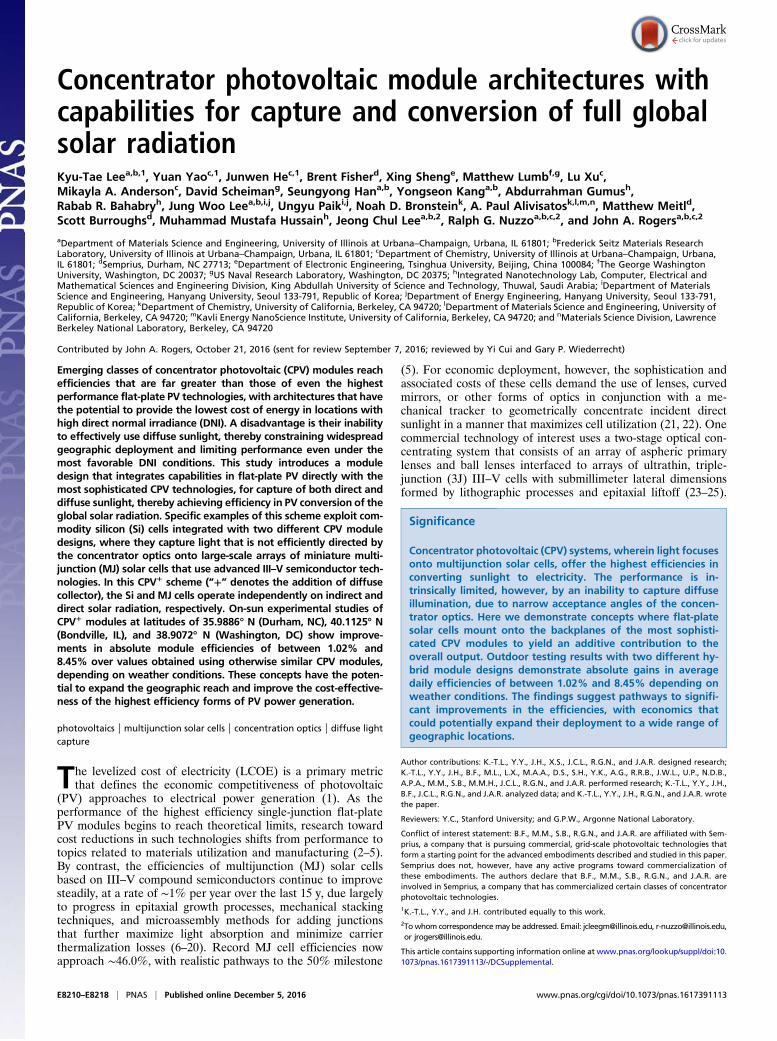
Results and DiscussionFig. 1A shows a schematic illustration of the working principlesof the HCPV+-DS design. Two-stage optics [i.e., a primary highconcentration (HC), inward-facing array of PCX lenses on a
Lee et al. PNAS | Published online December 5, 2016 | E8211
ENGINEE
RING
PNASPL
US
front panel, and a collection of secondary ball lenses mounteddirectly onto the 3J cells) concentrate direct sunlight (1,000×)onto the 3J cells (InGaP/GaAs/InGaAsNSb, 1.9 eV/1.4 eV/1.0 eV).Adjacent Si cells collect diffuse sunlight, which cannot be cap-tured effectively by the concentrating optics. These Si cells arelaser cut from larger, commercially available cells (interdigitatedback contact; A3000, SunPower Corp.) to sizes that fit the areasbetween the 3J cells, as illustrated in Fig. 1B. Representative I-Vcharacteristics from the unmodified HCPV module measuredunder flash test conditions (1,000 W·m−2, Tcell = 25 °C) and froman interconnected array of laser-cut Si cells under sun exposureoutdoors (950 W·m−2, measured without the primary lens) ap-pear in Fig. 1C. The HCPV module shows an open-circuitvoltage (Voc) of 105.2 V, a short-circuit current (Isc) of 1.09 A,and an energy conversion efficiency (η) of 34.0%. The array of Sicells has a Voc of 57.8 V, an Isc of 0.816 A, and an η of 18.5%.Photographs of the module backplane before and after integratingthe Si cells are in Fig. 1 D and E: The complete HCPV+-DSmodule consists of 660 3J cells (600 μm × 600 μm, intercellspacing: 20 mm) and 93 Si cells (16.1 mm × 127 mm) with a fullHCPV aperture area of 0.264 m2 and total Si cell area of0.190 m2. These components mount in a white powder-coatedsteel enclosure (636 mm × 476 mm × 68 mm) with a polymer-encapsulated copper backplane. The Si cells, interconnected inseries without bypass diodes, cover 72% of the available back-
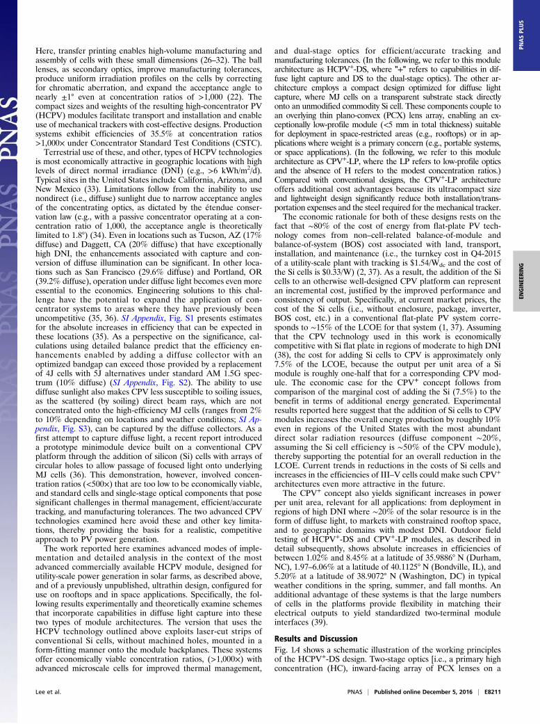
plane area. These components bond onto a white plastic in-sulating substrate for mechanical support and for ease ofintegration into the overall housing.The CPV+-LP embodiment provides complementary capabil-
ities and illustrates the versatility of the overall concepts. Here,an array of 3J cells mount on a transparent substrate with a formfactor (∼100 mm × 100 mm) designed to match that of com-modity Si cells, without modification (Maxeon, SunPower Corp.,η = 20% under 1 sun). Stacking these two subsystems and in-tegrating a corresponding set of single-stage low-concentration(LC) optics yields a complete module in which direct sunlightfocuses onto the array of microcells while the diffuse light strikesthe unmodified, underlying Si cell as illustrated in Fig. 2A. In anexample shown here, the optics consist of an array of glass LCoutward-facing PCX aspheres (18×) with thickness of 2.5 mmand focal length of 1 mm, in a hexagonal array with 3-mm pitch.The entire stack, as shown in Fig. 2B, provides for a low-profilemodule with a thickness that is less than 5 mm and a Si cellcoverage that approaches ∼100% (96% after taking the shadingby the 3J cells into account). Characteristic I-V performancecurves for the array of 3J cells and the Si cell appear in Fig. 2C.These data correspond to simultaneous measurements from asingle module on a tracker during an outdoor field test inWashington, DC under partly cloudy skies on March 3, 2016
Voltage (V)
Cur
rent
(A)
A B
C
D E
636 mm
476 mm
68 mm
0 20 40 60 80 100 1200.00.20.40.60.81.01.2
Si
HCPV-DS
Secondaryball lens
3J cell
Fig. 1. Schematic diagrams, images, and performance characteristics of anHCPV system that exploits dual-stage concentrator optics, with microscale 3Jcells to capture direct irradiation and Si solar cells to capture diffuse irradi-ation, which we refer to as an HCPV+-DS module. (A) Schematic illustrationof a unit cell in the module that highlights the two-stage optics design(1,000× concentration) and the interconnected array of the Si cells (bluerectangles) on the backplane in regions between the 3J cells with integratedball lenses (Inset), yielding a system that captures both direct (gray/blueshaded region) and diffuse (colored dashed lines to show representativetrajectories) solar radiation. (B) Schematic view at the module level (a col-lection of 32 unit cells). (C) Current (I)–voltage (V) curves for the HCPV-DSmodule (measured under CSTC from a flash test) and the interconnectedarray of Si cells (measured on sun outdoors). Photographs and magnifiedviews as insets showing (D) the standard HCPV-DS module panel backplaneconsisting of an array of the 3J cells coupled with ball lenses and (E) thehybrid HCPV+-DS module which includes the Si cells.
C
BLens array
CPV-LP array
Si Cell
CPV-LP Voltage (V)
CPV
-LP
Cur
rent
(mA) Si C
urrent (mA)
Si Voltage (V)
D0 20 40 60 80 100
0
10
20
300.0 0.2 0.4 0.6 0.8 1.0
0
200
400
600
800
E
A
100 mm
3 mm
Fig. 2. Schematic representations, photographs, and electrical performanceof a low-profile CPV system that exploits single-stage concentrator optics,with microscale 3J cells to capture direct irradiation and Si solar cells tocapture diffuse irradiation, which we refer to as a CPV+-LP. (A) Schematicillustration of a unit cell in the CPV-LP+ module that includes an array of 3Jcells on a transparent substrate located between a corresponding array offocusing lenses above and a single Si cell below. This system captures bothdirect (concentrated onto the 3J cells) and diffuse (illuminating the Si cell)solar irradiation. (B) Exploded view schematic illustration of the CPV-LP+
module design. (C) Current (I)–voltage (V) characteristics of the CPV-LPmodule and the Si cell (measured outdoors; blue for CPV; red for Si). (D andE) Photographs and zoom-in insets of a completed module of this type (i.e.,CPV+-LP) before and after the underlying Si cell integration.
E8212 | www.pnas.org/cgi/doi/10.1073/pnas.1617391113 Lee et al.
[global normal irradiance (GNI) = 1,053.0 W m−2; DNI = 682.2W m−2]. The 3J cell array operates at high voltage (Voc = 87.0 V)and low current (Isc = 21.9 mA), due to an electrical configu-ration of 34 parallel-connected strings of 30 series connectedcells, each of which generates over 3 V under CSTC. The Si cellyields correspondingly higher currents (Isc = 740 mA) and lowervoltages (Voc = 0.631 V). Fig. 2 D and E present optical imagesof the assembled device before and after integrating with theunderlying Si cell without a top LC outward-facing PCX lensarray. Fig. 2 D and E (Inset) images show a cell arrangement andan interconnection scheme.Diffuse solar radiation has a wide angular spread and follows a
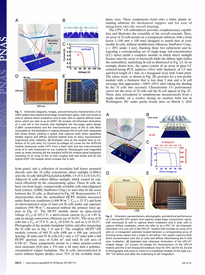
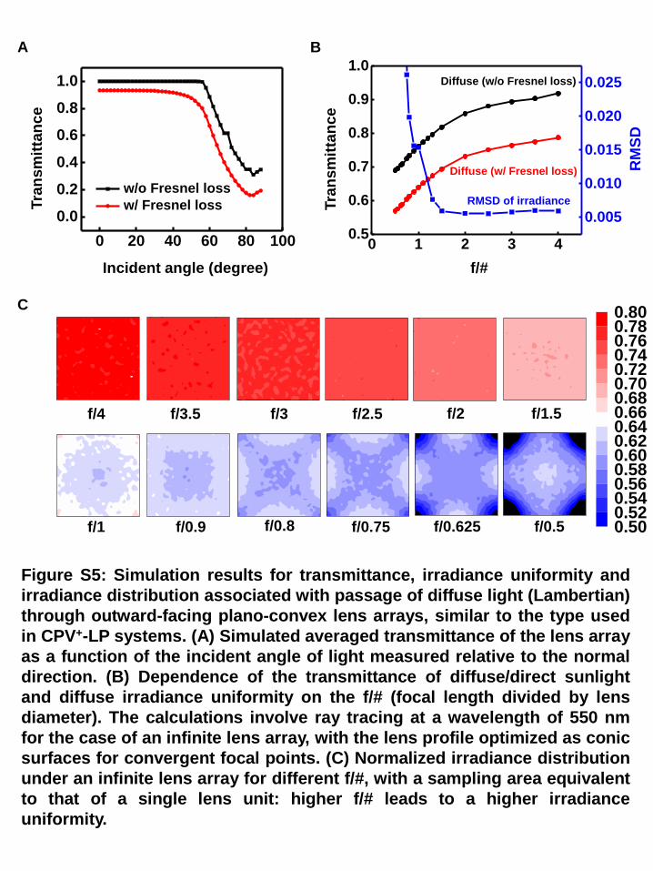
broad range of beam trajectories through the concentrating optics.As the angular distribution of diffuse irradiance can vary withmeteorological conditions, the calculations presented here assumea Lambertian distribution. For the front lens arrays in bothmodule architectures, the transmittance of light incident at variousincidence angles (θ) can be simulated by ray tracing (LightTools).Results for the primary, inward-facing HC PCX lens array in theHCPV-DS module (f/# = focal length/lens diameter = 3) appearin Fig. 3A. At incidence angles greater than 30°, the transmittancesuffers from total internal reflection (TIR) within the array, ashighlighted by calculations that do not consider Fresnel reflectionlosses (black curves in Fig. 3A; see SI Appendix, Fig. S4 for raypath illustrations). These losses (both TIR and Fresnel) continueto increase as the incidence angle increases. Similar trends appearin simulations for the outward-facing LC PCX lens array for theCPV-LP module (f/# = 2.3; SI Appendix, Fig. S5).The averaged transmittance of diffuse light through a PCX
lens unit in either module design is also related to its focusingpower. As shown by the simulated results in Fig. 3B and SIAppendix, Fig. S5, larger values of f/# (i.e., a smaller focusingpower) lead to higher transmittance due to reduced TIR losseswithin the PCX lens, whereas the Fresnel losses (difference be-
tween the red and black curves) remain nearly constant. The f/#also influences the irradiance distribution on the focal plane, asshown by the calculated results in Fig. 3C and SI Appendix, Fig. S5.The spatial uniformity of these irradiance profiles can be definedby their root-mean-square deviation (RMSD), according to
RMSD =
ffiffiffiffiffiffiffiffiffiffiffiffiffiffiffiffiffiffiffiffiffiffiffiffiffiffiffiffiffiffiffiffiffiffiffiffiffiffiffiffiffiffi1
n− 1
Xni=1
�IiIavg
− 1�2
vuut , [1]
where Ii is the irradiance of a sampling pixel at some location andIavg is the overall averaged irradiance on the panel backplane. Aspresented in Fig. 3B and SI Appendix, Fig. S5, the RMSD rea-ches negligible values when the f/# is larger than 2. The PCXlens arrays in both module architectures fulfill this criterion.Similar ray-tracing methods can simulate the distribution of
diffuse irradiance that forms on both types of module backplanesafter passage through the PCX lens array. This quantity is im-portant for efficient capture and conversion by the Si cells.Calculations, again assuming Lambertian angular distribution forthe incoming diffuse light, for the HCPV+-DS module revealthese distributions for three different sidewall reflectivity con-ditions (mirror, diffuse, and absorbing), as shown in Fig. 4.Reflecting sidewalls (i.e., 100% specular reflection) generate themost even backplane diffuse light distribution (RMSD = 0.0059;Fig. 4A), equivalent to the case of an infinite lens array whereprojections of diffuse light through multiple single lenses (SIAppendix, Fig. S6) overlap to create uniform irradiance. Theoverall optical efficiency (ηop) for passage of diffuse lightthrough the primary lens array and arrival at the backplane is76%, restricted by losses from Fresnel reflections (11%) andlimited acceptance angles for photons at large incidence anglesdue to TIR within the primary lens array (13%). For the case of a10% diffuse light component in the incident solar illumination,
0 1 2 3 40.5
0.6
0.7
0.8
0.9
1.0
0.005
0.010
0.015
0.020
0.025Diffuse (w/o Fresnel loss)
RMSD of irradiance
Diffuse (w/ Fresnel loss)
Incident angle (degree)
Tran
smitt
ance
f/4 f/3.5 f/3 f/2.5 f/2 f/1.5
f/1 f/0.9 f/0.8 f/0.75 f/0.625 f/0.5
Tran
smitt
ance
f/#
RM
SD
0.500.520.540.560.580.600.620.640.660.680.700.720.740.760.780.80
0 20 40 60 80 1000.0
0.2
0.4
0.6
0.8
1.0
w/o Fresnel lossw/ Fresnel loss
A B
C
Fig. 3. Simulation results for transmittance, irradiance uniformity, and irradiance distribution associated with passage of diffuse light (Lambertian) throughinward-facing HC plano-convex lens arrays in the HCPV+-DS systems. (A) Simulated averaged transmittance of the lens array as a function of the incidentangle of light measured relative to the normal direction. (B) Dependence of the transmittance of diffuse sunlight and diffuse irradiance uniformity on the f/#(focal length divided by lens diameter). The calculations involve ray tracing at a wavelength of 550 nm for the case of an infinite lens array, with the lensprofile optimized as conic surfaces for convergent focal points. (C) Normalized irradiance distribution under an infinite lens array for different f/#, with asampling area equivalent to that of a single lens unit: higher f/# leads to a higher irradiance uniformity.
Lee et al. PNAS | Published online December 5, 2016 | E8213
ENGINEE
RING
PNASPL
US
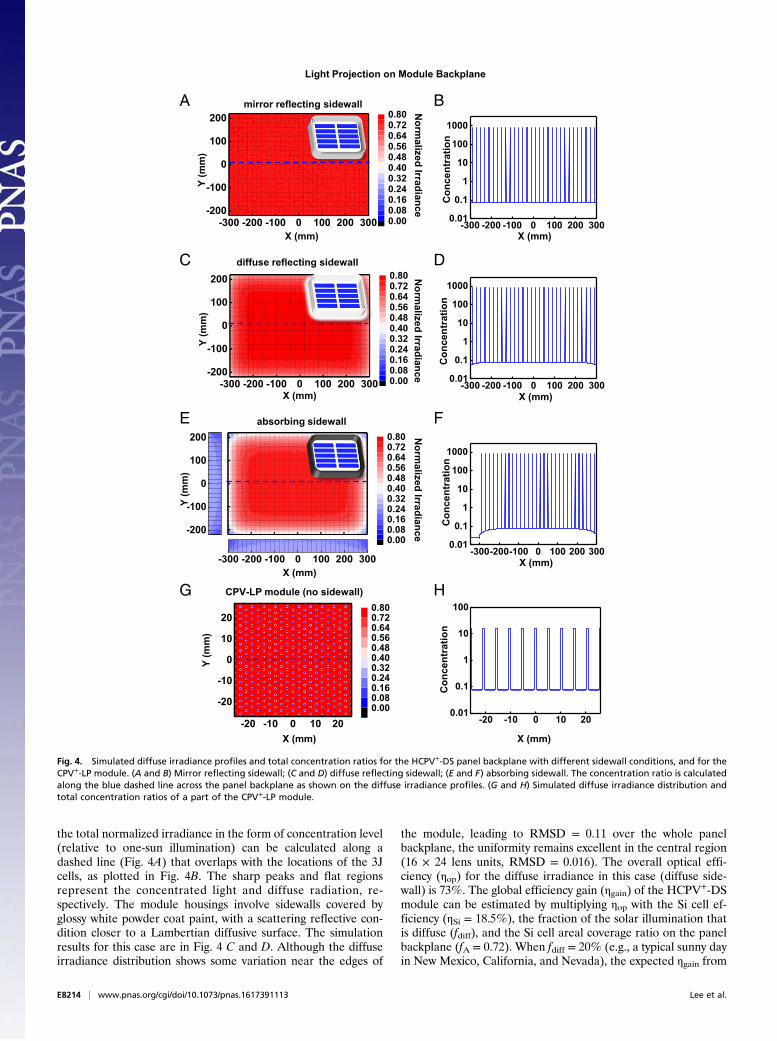
the total normalized irradiance in the form of concentration level(relative to one-sun illumination) can be calculated along adashed line (Fig. 4A) that overlaps with the locations of the 3Jcells, as plotted in Fig. 4B. The sharp peaks and flat regionsrepresent the concentrated light and diffuse radiation, re-spectively. The module housings involve sidewalls covered byglossy white powder coat paint, with a scattering reflective con-dition closer to a Lambertian diffusive surface. The simulationresults for this case are in Fig. 4 C and D. Although the diffuseirradiance distribution shows some variation near the edges of
the module, leading to RMSD = 0.11 over the whole panelbackplane, the uniformity remains excellent in the central region(16 × 24 lens units, RMSD = 0.016). The overall optical effi-ciency (ηop) for the diffuse irradiance in this case (diffuse side-wall) is 73%. The global efficiency gain (ηgain) of the HCPV+-DSmodule can be estimated by multiplying ηop with the Si cell ef-ficiency (ηSi = 18.5%), the fraction of the solar illumination thatis diffuse (fdiff), and the Si cell areal coverage ratio on the panelbackplane (fA = 0.72). When fdiff = 20% (e.g., a typical sunny dayin New Mexico, California, and Nevada), the expected ηgain from
-300 -200 -100 0 100 200 3000.01
0.1
1
10
100
1000
-300 -200 -100 0 100 200 3000.01
0.1
1
10
100
1000
-300 -200 -100 0 100 200 300-200
-100
0
100
200
0.000.080.160.240.320.400.480.560.640.720.80
Y (m
m)
X (mm)
diffuse reflecting sidewall
Norm
alized Irradiance
C
0.000.080.160.240.320.400.480.560.640.720.80
-200
-100
0
100
200
-300 -200 -100 0 100 200 300
absorbing sidewallE
X (mm)
Y (m
m)
Norm
alized Irradiance
X (mm)
Con
cent
ratio
nC
once
ntra
tion
X (mm)
Light Projection on Module Backplane
-300-200-100 0 100 200 3000.01
0.1
1
10
100
1000
D
F
mirror reflecting sidewallA
-300 -200 -100 0 100 200 300-200
-100
0
100
200
0.000.080.160.240.320.400.480.560.640.720.80
X (mm)
Y (m
m)
Norm
alized Irradiance
Con
cent
ratio
n
X (mm)
B
-20 -10 0 10 20
-20
-10
0
10
20
0.000.080.160.240.320.400.480.560.640.720.80
-20 -10 0 10 200.01
0.1
1
10
100H
Con
cent
ratio
n
X (mm)
CPV-LP module (no sidewall)G
X (mm)
Y (m
m)
Fig. 4. Simulated diffuse irradiance profiles and total concentration ratios for the HCPV+-DS panel backplane with different sidewall conditions, and for theCPV+-LP module. (A and B) Mirror reflecting sidewall; (C and D) diffuse reflecting sidewall; (E and F) absorbing sidewall. The concentration ratio is calculatedalong the blue dashed line across the panel backplane as shown on the diffuse irradiance profiles. (G and H) Simulated diffuse irradiance distribution andtotal concentration ratios of a part of the CPV+-LP module.
E8214 | www.pnas.org/cgi/doi/10.1073/pnas.1617391113 Lee et al.
the array of the Si cells is fdiff × ηop × ηSi × fA = 1.9%. Incomplete overcast conditions (fdiff = 100%), the estimated effi-ciency gain from the Si cells reaches 9.7% (assuming ηSi remainsthe same under the cloudy sky spectra). An unmodified HCPVsystem ceases to function under such circumstances. Furtherimprovements are possible through the addition of Si cells on thesidewalls to reach ηop = 76%. Such schemes involve, however,additional costs and they significantly increase nonuniformitiesin the irradiance distribution on the sidewalls and backplane(The RMSD of irradiance profile on the backplane is 0.18, Fig.4E). Furthermore, the irradiance on the sidewall is only ∼1/3 ofthat of the center of the backplane (Fig. 4F), which would resultin a voltage drop in the Si cells that may not be fully compen-sated by the gain in optical efficiency.Corresponding results for the CPV+-LP system appear in Fig.
4 G and H. Here, ηop is 75.6%, mainly limited by optical lossesfrom the top lens array, following considerations that are similarto those associated with the primary optic in the HCPV+-DSdesign. For this type of module (ηop = 75.6%, ηSi = 20%,
fA = 0.96), the expected ηgain is 2.9% and 14.5% on sunny (fdiff =20%) and overcast (fdiff = 100%) days, respectively, both ofwhich exceed values estimated for the HCPV+-DS architecturedue to the improved Si cell coverage.Outdoor testing of HCPV+-DS modules on a two-axis solar
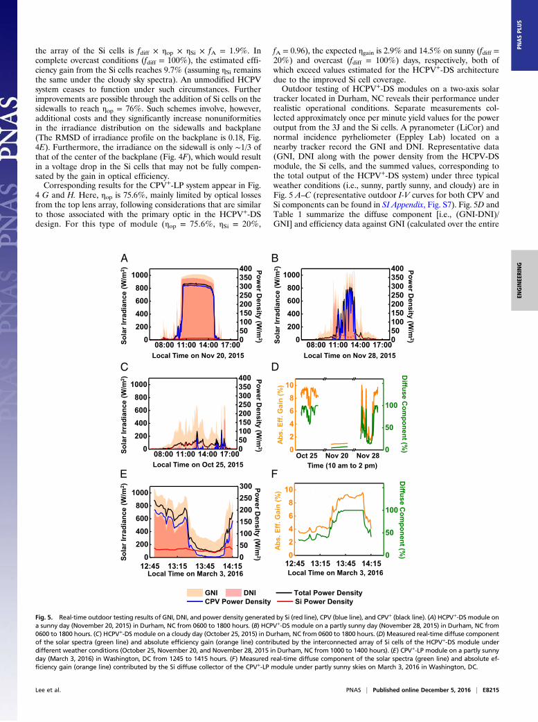
tracker located in Durham, NC reveals their performance underrealistic operational conditions. Separate measurements col-lected approximately once per minute yield values for the poweroutput from the 3J and the Si cells. A pyranometer (LiCor) andnormal incidence pyrheliometer (Eppley Lab) located on anearby tracker record the GNI and DNI. Representative data(GNI, DNI along with the power density from the HCPV-DSmodule, the Si cells, and the summed values, corresponding tothe total output of the HCPV+-DS system) under three typicalweather conditions (i.e., sunny, partly sunny, and cloudy) are inFig. 5 A–C (representative outdoor I-V curves for both CPV andSi components can be found in SI Appendix, Fig. S7). Fig. 5D andTable 1 summarize the diffuse component [i.e., (GNI-DNI)/GNI] and efficiency data against GNI (calculated over the entire
08:00 11:00 14:00 17:000200400600800
1000
050100150200250300350400
Sola
r Irr
adia
nce
(W/m
2 )
Local Time on Nov 20, 2015
Power D
ensity (W/m
2) Sola
r Irr
adia
nce
(W/m
2 )
Local Time on Nov 28, 2015
Power D
ensity (W/m
2)So
lar I
rrad
ianc
e (W
/m2 )
Local Time on Oct 25, 2015
Power D
ensity (W/m
2)
Oct 25 Nov 20 Nov 28
Abs.
Eff.
Gai
n (%
)
Time (10 am to 2 pm)
Diffuse C
omponent (%
)
GNI DNI Total Power Density CPV Power Density Si Power Density
08:00 11:00 14:00 17:000200400600800
1000
050100150200250300350400
08:00 11:00 14:00 17:000200400600800
1000
050100150200250300350400
12:45 13:15 13:45 14:150
200400600800
1000
050100150200250300
Sola
r Irr
adia
nce
(W/m
2 )
Local Time on March 3, 2016
Power D
ensity (W/m
2)
12:45 13:15 13:45 14:1502468
10
0
50
100
Abs.
Eff.
Gai
n (%
)
Local Time on March 3, 2016
Diffuse C
omponent (%
)
02468
10
0
50
100
A
C
E F
D
B
Fig. 5. Real-time outdoor testing results of GNI, DNI, and power density generated by Si (red line), CPV (blue line), and CPV+ (black line). (A) HCPV+-DS module ona sunny day (November 20, 2015) in Durham, NC from 0600 to 1800 hours. (B) HCPV+-DS module on a partly sunny day (November 28, 2015) in Durham, NC from0600 to 1800 hours. (C) HCPV+-DS module on a cloudy day (October 25, 2015) in Durham, NC from 0600 to 1800 hours. (D) Measured real-time diffuse componentof the solar spectra (green line) and absolute efficiency gain (orange line) contributed by the interconnected array of Si cells of the HCPV+-DS module underdifferent weather conditions (October 25, November 20, and November 28, 2015 in Durham, NC from 1000 to 1400 hours). (E) CPV+-LP module on a partly sunnyday (March 3, 2016) in Washington, DC from 1245 to 1415 hours. (F) Measured real-time diffuse component of the solar spectra (green line) and absolute ef-ficiency gain (orange line) contributed by the Si diffuse collector of the CPV+-LP module under partly sunny skies on March 3, 2016 in Washington, DC.
Lee et al. PNAS | Published online December 5, 2016 | E8215
ENGINEE
RING
PNASPL
US
module area) extracted from these measurements (similar dataextracted from outdoor testing in Bondville, IL are presented in SIAppendix, Fig. S8). For the case of the sunny day (November 20,2015, Fig. 5A), the DNI is over 90% and is stable (red shaded area,∼900 W/m2) throughout the day. Here, the HCPV-DS powerdensity (blue curve) peaks at 309.4 W/m2 (12:19 PM) and reaches anaverage global efficiency (ηHCPV-DS) of 29.5% between 11:00 AMand 4:00 PM (note that the efficiency against the DNI is 31.9%here). The Si cells provide an added power density of 9.57 W/m2 atthe same time (red curve), which translates to an averaged absoluteglobal efficiency gain of 1.02% when the averaged diffuse compo-nent is 7.64%, to enable ηHCPV
+-DS = 30.5% (global). On the partly
sunny day (November 28, 2015, Fig. 5B), the DNI remains relativelyhigh (∼450 W/m2 on average) although with strong transient varia-tions due to clouds. The result is a peak HCPV-DS power densityof 280.7 W/m2 at 12:36 PM (DNI = 884 W/m2) and averagedηHCPV-DS = 16.9% (global; 29.8% against DNI). The Si cells (peakpower density 43.6 W/m2 at 1:13 PM) add 4.36% to the aver-aged global efficiency due to the increased diffuse illumination(fdiffuse= 43.5%), thereby yielding averaged ηHCPV
+-DS = 21.2%
(global). The total power density from the HCPV+-DS herepeaks at 12:36 PM with a value of 296.5 W/m2. By contrast,under cloudy conditions (October 25, 2015, Fig. 5C), ηHCPV-DS(global) drops to 1.73%. Here, when the diffuse component is84.4%, the Si cells produce a peak power density of 43.1 W/m2
at 12:28 PM, and add 8.45% to the averaged global efficiency, toenable ηHCPV
+-DS = 10.2% (global). As expected, the data in
Fig. 5D show that the absolute efficiency gain provided by the Sicells follows the trend of the diffuse component of incident ra-diation, with average cell efficiencies (calculated using only the areaof the Si cells) of 18.4% (sunny, November 20) and 13.9% (partlysunny, November 28 and cloudy, October 25) against diffuse irra-diance. The latter value matches predictions by optical simulation(ηop × ηSi = 0.73 × 0.185 = 13.5%). The former exceeds simulation,likely because the Si cell can generate additional power from DNIscattered from intersections between lens arrays and/or imperfec-tions in the lens surfaces (SI Appendix, Fig. S9).Outdoor field test measurements with a CPV+-LP module in
Washington, DC on a partly sunny day (March 3, 2016) provideoperational insights similar to those described above. The mea-sured DNI and GNI, together with the power density generatedby the CPV+-LP module, appear in Fig. 5E. As with the HCPV+-DSsystem, the maximum power generated by the 3J cell array fol-lows the DNI profile whereas the output power from the Si cellremains fairly constant, following the trend of the diffuse irra-diance (i.e., GNI-DNI). The efficiency of the 3J cell arraymeasured in the integrated module (i.e., with optical losses fromthe lens array) against DNI is ∼30%; that of the Si cell relative tothe diffuse irradiance is ∼10% (dashed orange lines in Fig. 5F).This Si efficiency includes effects of shading losses associatedwith the grid interconnects and the 3J cells as well as reflectionlosses associated with the concentration optics and the glasssupport for the 3J cell array. Compared with the previously de-scribed design, the glass support represents an additional sourceof loss, partly compensated by the improved coverage of the Sicell (nearly 100%), such that a similar level of averaged globalefficiency gain (5.20%) relative to the averaged diffuse compo-nent (54.3%) results, as shown in Fig. 5F. The averaged effi-
ciency of a CPV-LP module against GNI is 13.8%, whereas theCPV+-LP system reaches 19.0% on this particular day. The data,as provided in SI Appendix, Fig. S9, indicate a linear relationshipbetween the output power from the Si cells and the diffuse ir-radiance (GNI-DNI). Interestingly, the data from the Si cell aremore tightly correlated with diffuse power at low levels of DNI(<300 W/m2, black points) than at high levels (red points). Thisobservation again suggests that the DNI lost by scattering fromthe lens array intersections and imperfections on the lens sur-faces is recycled by the Si cell, similar to the effects describedpreviously for the HCPV+-DS modules (SI Appendix, Fig. S9).For both types of CPV+ modules, the low per-area cost of
energy from Si cells makes them attractive for use on the modulebackplane as diffuse light collectors. Emerging alternatives basedon perovskites, organics, epitaxial lift-off III–Vs, each with the ad-ditional possibility of use in advanced luminescent concentration
Table 1. Summary of measured PV characteristics of Si, CPV, and CPV+ modules on different weather conditions
Condition Date Diffuse component, % CPV+ efficiency, % CPV efficiency, % Si efficiency, %
Sunny 20 November 2015 7.64 30.5 29.5 1.02Partly sunny 28 November 2015 43.5 21.2 16.9 4.36Cloudy 25 October 2015 84.4 10.2 1.73 8.45Partly sunny 3 March 2016 54.3 19.0 13.8 5.20
1.0 2.0 3.01.0
2.0
3.0
4.0
0.0
1.3
2.6
3.9
5.2
Bandgap (eV)
Air
Mas
s
Abs. Eff. Gain (%
)
Bandgap (eV)
Aero
sol O
ptic
al D
epth
(τ)
Abs. Eff. Gain (%
)
A
B
1.0 2.0 3.00.0
0.2
0.4
0.6
0.8
1.0
0.00
4.80
9.60
14.4
19.2
Fig. 6. Detailed balance limit of the absolute efficiency gain from diffuselight capture as a function of (A) air mass number and cell bandgap (τ =0.08); (B) aerosol optical depth and cell bandgap (AM = 1.5).
E8216 | www.pnas.org/cgi/doi/10.1073/pnas.1617391113 Lee et al.
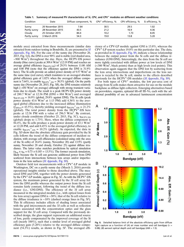
schemes (31, 40–45), may also be considered. The bandgaps,in particular, are important. Fig. 6A presents the detailed bal-ance limit for the absolute efficiency gain from diffuse lightcapture as a function of the cell bandgap and the air mass value,calculated based on the simulation package SMARTS (46, 47).At AM 1.5, with panel tilting angle tracking the sun, rather thana fixed 37° tilt angle used for the standard ASTM G173-03 ref-erence spectrum (see SI Appendix, Fig. S10 for comparison), theabsolute efficiency gain from diffuse light capture (i.e., the dif-ference between the tilted GNI and DNI) peaks at a bandgap of1.41 eV, which is different from the values (1.14 and 1.34 eV)optimized for the full spectrum conversion (3). This differencefollows from the increased weight of the diffuse solar spectrum inthe visible band compared with the full solar spectrum (SI Ap-pendix, Fig. S11). The maximal efficiency gain (4.6% at 1.41 eV,with a diffuse component of 13%) is ∼0.5% higher than thatpredicted for Si (4.1% at 1.11 eV). As the atmosphere becomesthicker (i.e., higher AM value), the achievable efficiency gaintends to increase slightly due to the increased diffuse component,with the optimum bandgap shifting to a smaller values due tospectral variation. An ∼5% gain in efficiency is theoreticallypossible under thick air mass numbers (e.g., AM = 4). Increasesin atmospheric turbidity, either in the form of soil dust or airpollution, lead to further increases in the diffuse component. Fig.6B shows the detailed balance limit for the efficiency gain fromdiffuse light capture as a function of single-junction bandgap andthe aerosol optical depth (τ) under AM 1.5 condition. In “cleanair” (τ = 0.1) 5.0% absolute efficiency gain is expected at abandgap of 1.37–1.56 eV, whereas in “smoky/foggy air” (τ = 0.8)17.1% absolute efficiency boost is possible with a bandgap of1.37–1.44 eV. Such simulations suggest value in custom back-plane cell designs that optimizes the cell bandgap for differentterrestrial and climate conditions.In addition to the careful selection of cell bandgaps for diffuse
light utilization, several other strategies can improve the effi-ciencies of the two CPV+ modules introduced here. The per-formance of the CPV+-LP system can be enhanced by: (i)mitigating reflection losses from lens surfaces by introducing fullspectrum antireflection (AR) coatings with broad acceptanceangles, with the potential for increasing the optical efficiency by8% for direct light (i.e., 4% at each interface) and from 76% to88% for diffuse light; (ii) reducing the reflections losses from thetransparent substrate that supports the arrays of 3J cells, byadding the AR layer on top and an index matching liquid un-derneath to fill the air gap between the substrate and the Si cell,with the potential to improve the optical efficiency by 8% fordiffuse light; (iii) increasing the concentration ratio to hundredsof suns, with the potential to increase the efficiency for directsunlight by ∼3%; and (iv) incorporating world-record MJ cells(∼46% efficiency), with the potential to increase the efficiencyfor direct light by 9%. Extrapolations based on implementing allof these enhancements combined with the use of cells with op-timized bandgap for diffuse light [GaAs ∼ 1.4 eV, optimized forAM = 1.5, η = 28.8% (5)], suggest that the global efficiency forthe CPV+-LP module measured on a partly sunny day (54.3%diffuse) like the one in Table 1 can be improved from 19.0% to28.8%, whereas on a sunny day (10% diffuse), projected globalefficiency can be improved from 28.9% to 35.2%. These im-
proved efficiency values for the CPV+-LP systems are compa-rable to, and can even exceed, world-record flat-plate modulesformed by epitaxial growth [InGaP/GaAs dual junction fromAlta Devices, η = 31.6% (5)].For the HCPV+-DS system, besides (i) using the AR coatings
on lens surfaces (8% enhancement for direct light, 19% for diffuselight) and (ii) using the world-record MJ cells (9% enhancementfor direct light) as mentioned earlier, the efficiency can alsobenefit from (iii) increasing the Si cell coverage on the backplanefrom 72% to nearly 100%. The collective impact of changes (i)–(iii), together with use of cells that have optimized bandgaps(GaAs ∼ 1.4 eV, η = 28.8%) could improve the module effi-ciencies reported in Table 1 from 30.5% to 36.6% (for sunny days)and from 21.2% to 30.8% (for partly sunny days).For both CPV+ module designs, these enhancements corre-
spond to significant gains in annual average efficiency at variousgeographic locations in the United States (see the Future In-novations chart in SI Appendix, Fig. S1) In high DNI regions suchas Tucson [with an annual diffuse radiation component (fdiff,avg)of 17.0%)] and Daggett (fdiff,avg = 20.2%), the yearly averageabsolute increases in efficiency (Δηdiff,avg) by adding the diffusecollector are 3.8% and 4.6%, respectively, whereas in mediumDNI regions with more frequent overcast conditions such as SanFrancisco (fdiff,avg = 29.6%) and Portland (fdiff,avg = 39.2%),Δηdiff,avg reaches 6.7% and 8.8%, respectively. Data from in-stallation in these and others regions of the world may yield datauseful for detailed LCOE analyses in future work.
ConclusionsIn summary, this paper demonstrates schemes by which advancedCPV module technologies can be readily converted into systemscapable of capturing and converting both direct and diffuse solarradiation, with potentially important consequences on the cost ofenergy for photovoltaics. Outdoor testing results in Durham, NC, inBondville, IL, and in Washington, DC indicate absolute increases indaily averaged module efficiencies between 1.02% and 8.45%,measured against GNI solar radiation, depending on weatherconditions. Exploiting improved AR coatings on the concentratingoptics and glass surfaces and implementing optimized bandgaps forthe flat-plate PV materials offer near-term potential for furthersignificant improvements in the performance characteristics. Fur-thermore, because these module architectures are independent ofthe MJ cell designs, immediate improvements in module effi-ciencies may be possible by leveraging future advances in MJ celltechnology. The overall results suggest promising routes towardhigh-efficiency PV platforms, suitable wide geographic deployment.
ACKNOWLEDGMENTS. This work is part of the "Light-Material Interactionsin Energy Conversion" Energy Frontier Research Center (to K.-T.L., Y.Y., J.H.,X.S., L.X., M.A.A., N.D.B., A.P.A., R.G.N., and J.A.R.) funded by the US De-partment of Energy, Office of Science, Office of Basic Energy Sciences underAward DE-SC0001293. The work presented here was funded in part by theAdvanced Research Projects Agency-Energy, US Department of Energy, un-der Award DE-AR0000624. J.W.L. and U.P. are supported by the Global Re-search Laboratory Program (K20704000003TA050000310) through the NationalResearch Foundation of Korea funded by the Ministry of Science. A.G., R.R.B.,and M.M.H. are supported by the King Abdullah University of Science andTechnology Technology Transfer Office under Award GEN/1/4014-01-01. X.S.acknowledges support from National Natural Science Foundation of China(Project 51602172).
1. Branker K, Pathak MJM, Pearce JM (2011) A review of solar photovoltaic levelized cost
of electricity. Renew Sustain Energy Rev 15(9):4470–4482.2. Luque A, Hegedus S (2011) Handbook of Photovoltaic Science and Engineering (Wiley,
Chichester, UK).3. Shockley W, Queisser HJ (1961) Detailed balance limit of efficiency of p‐n junction
solar cells. J Appl Phys 32(3):510–519.4. Polman A, Atwater HA (2012) Photonic design principles for ultrahigh-efficiency
photovoltaics. Nat Mater 11(3):174–177.5. Green MA, Emery K, Hishikawa Y, Warta W, Dunlop ED (2016) Solar cell efficiency
tables (version 48). Prog Photovolt Res Appl 24(7):905–913.
6. Luque A (2011) Will we exceed 50% efficiency in photovoltaics? J Appl Phys 110:031301.7. Derkacs D, Jones-Albertus R, Suarez F, Fidaner O (2012) Lattice-matched multijunction
solar cells employing a 1 eV GaInNAsSb bottom cell. J Photon Energy 2:021805.8. King RR, et al. (2007) 40% efficient metamorphic GaInP/GaInAs/Ge multijunction solar
cells. Appl Phys Lett 90:183516.9. Geisz JF, et al. (2007) High-efficiency GaInP/GaAs/InGaAs triple-junction solar cells
grown inverted with a metamorphic bottom junction. Appl Phys Lett 91:023502.10. King RR, et al. (2009) Band-gap-engineered architectures for high-efficiency multi-
junction concentrator solar cells. The 24th European Photovoltaic Solar Energy Confer-
ence and Exhibition (WIP-Renewable Energies, Hamburg, Germany), pp 55–61.
Lee et al. PNAS | Published online December 5, 2016 | E8217
ENGINEE
RING
PNASPL
US
11. Wojtczuk S, et al. (2011) 42% 500X bi-facial growth concentrator cells. AIP Conf Proc1407:9–12.
12. Sasaki K, et al. (2013) Development of InGaP/GaAs/InGaAs inverted triple junctionconcentrator solar cells. AIP Conf Proc 1556:22–25.
13. Sheng X, et al. (2014) Printing-based assembly of quadruple-junction four-terminal mi-croscale solar cells and their use in high-efficiency modules. Nat Mater 13(6):593–598.
14. Tanabe K, Watanabe K, Arakawa Y (2012) III-V/Si hybrid photonic devices by directfusion bonding. Sci Rep 2:349.
15. Zhao L, Flamand G, Poortmans J (2010) Recent progress and spectral robustness studyfor mechanically stacked multi-junction solar cells. AIP Conf Proc 1277:284–289.
16. Dimroth F, et al. (2014) Wafer bonded four-junction GaInP/GaAs/GaInAsP/GaInAsconcentrator solar cells with 44.7% efficiency. Prog Photovolt Res Appl 22:277–282.
17. Derendorf K, et al. (2013) Fabrication of GaInP/GaAs//Si solar cells by surface activateddirect wafer bonding. IEEE J Photovolt 3:1423–1428.
18. Takamoto T, et al. (1997) InGaP/GaAs and InGaAs mechanically-stacked triple-junctionsolar cells. The 26th IEEE Photovoltaic Specialists Conference (IEEE, Anaheim, CA), pp1031–1034.
19. Gee JM, Virshup GF (1988) A 31% efficient GaAs/silicon mechanically stacked, mul-tijunction concentrator solar cell. The 20th IEEE Photovoltaic Specialists Conference(IEEE, Las Vegas, NV), 1:754–758.
20. Fraas LM, et al. (1990) Over 35% efficient GaAs/GaSb stacked concentrator cell as-semblies for terrestrial applications. The 21st IEEE Photovoltaic Specialists Conference(IEEE, Kissimmee, FL), Vol 1, pp 190–195.
21. Chong K-K, Lau S-L, Yew T-K, Tan PC-L (2013) Design and development in optics ofconcentrator photovoltaic system. Renew Sustain Energy Rev 19:598–612.
22. Menard E, et al. (2011) Optics development for micro-cell based CPV modules. ProcSPIE 8108:810805.
23. Ghosal K, Burroughs S, Heuser K, Setz D, Garralaga-Rojas E (2013) Performance resultsfrom micro-cell based high concentration photovoltaic research development anddemonstration systems. Prog Photovolt Res Appl 21(6):1370–1376.
24. Ghosal K, et al. (2014) Semprius field results and progress in system development. IEEEJ Photovolt 4(2):703–708.
25. Kurtz S, et al. (2015) Key parameters in determining energy generated by CPVmodules. Prog Photovolt Res Appl 23(10):1250–1259.
26. Carlson A, Bowen AM, Huang Y, Nuzzo RG, Rogers JA (2012) Transfer printingtechniques for materials assembly and micro/nanodevice fabrication. Adv Mater24(39):5284–5318.
27. Burroughs S, et al. (2010) A new approach for a low cost CPV module design utilizingmicro‐transfer printing technology. AIP Conf Proc 1277(1):163–166.
28. Bower CA, Menard E, Garrou PE (2008) Transfer printing: An approach for massivelyparallel assembly of microscale devices. 58th Electronic Components and TechnologyConference, 2008, ECTC 2008 (IEEE, Lake Buena Vista, FL), pp 1105–1109.
29. Furman B, et al. (2010) A high concentration photovoltaic module utilizing micro-transfer printing and surface mount technology. Photovoltaic Specialists Conference(PVSC), 2010 35th IEEE (IEEE, Honolulu), pp 000475–000480.
30. Yoon J, et al. (2010) GaAs photovoltaics and optoelectronics using releasable multi-
layer epitaxial assemblies. Nature 465(7296):329–333.31. Yoon J, et al. (2011) Flexible concentrator photovoltaics based on microscale silicon
solar cells embedded in luminescent waveguides. Nat Commun 2:343.32. Yao Y, Brueckner E, Li L, Nuzzo R (2013) Fabrication and assembly of ultrathin high-
efficiency silicon solar microcells integrating electrical passivation and anti-reflection
coatings. Energy Environ Sci 6(10):3071–3079.33. Denholm P, et al. (2012) The potential role of concentrating solar power in enabling
high renewables scenarios in the United States. Technical Report (National Renew-
able Energy Laboratory, Golden, CO), pp TP-6A20-56294.34. Hernández M, et al. (2007) The XR nonimaging photovoltaic concentrator.
Proceedings of SPIE, Nonimaging Optics and Efficient Illumination Systems IV (SPIE,
San Diego), Vol 6670, pp 667005–667010.35. Marion W, Wilcox S (1994) Solar Radiation Data Manual for Flat-Plate And
Concentrating Collectors (National Renewable Energy Laboratory, Golden, CO), pp
1–252.36. Yamada N, Okamoto K (2014) Experimental measurements of a prototype high
concentration Fresnel lens CPV module for the harvesting of diffuse solar radiation.
Opt Express 22(Suppl 1):A28–A34.37. Anonymous (2015) Solar Market Insight 2015:Q4 (Solar Energy Industries Association,
Boston).38. Kost C, et al. (2013) Levelized Cost of Electricity Renewable Energy Technologies
Study (Fraunhofer ISE, Freiburg, Germany).39. Menard E, et al. (2011) Multi-physics circuit network performance model for CPV
modules/systems. Photovoltaic Specialists Conference (PVSC), 2011 37th IEEE (IEEE,
Seattle), pp 002268–002272.40. Bronstein ND, et al. (2014) Luminescent solar concentration with semiconductor
nanorods and transfer-printed micro-silicon solar cells. ACS Nano 8(1):44–53.41. Sheng X, et al. (2013) Doubling the power output of bifacial thin-film GaAs solar cells
by embedding them in luminescent waveguides. Adv Energy Mater 3(8):991–996.42. Sheng X, et al. (2013) Enhanced ultraviolet responses in thin-film InGaP solar cells by
down-shifting. Phys Chem Chem Phys 15(47):20434–20437.43. Bronstein ND, et al. (2015) Quantum dot luminescent concentrator cavity exhibiting
30-fold concentration. ACS Photonics 2(11):1576–1583.44. Xu L, et al. (2016) Enhanced photon collection in luminescent solar concentrators with
distributed Bragg reflectors. ACS Photonics 3(2):278–285.45. Boriskina SV, et al. (2016) Roadmap on optical energy conversion. J Opt 18(7):073004.46. Gueymard C (1995) SMARTS2: A Simple Model of the Atmospheric Radiative Transfer
of Sunshine: Algorithms and Performance Assessment (Florida Solar Energy Center,
Cocoa, FL), pp 1–78.47. Gueymard CA (2001) Parameterized transmittance model for direct beam and cir-
cumsolar spectral irradiance. Sol Energy 71(5):325–346.
E8218 | www.pnas.org/cgi/doi/10.1073/pnas.1617391113 Lee et al.
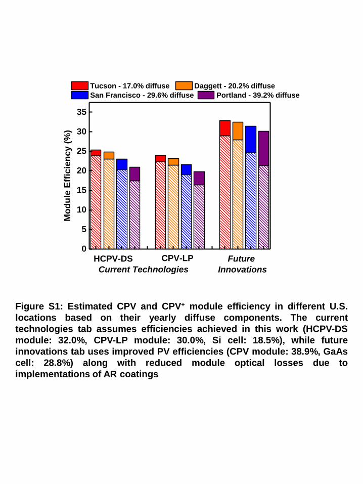
Figure S1: Estimated CPV and CPV+ module efficiency in different U.S.
locations based on their yearly diffuse components. The current
technologies tab assumes efficiencies achieved in this work (HCPV-DS
module: 32.0%, CPV-LP module: 30.0%, Si cell: 18.5%), while future
innovations tab uses improved PV efficiencies (CPV module: 38.9%, GaAs
cell: 28.8%) along with reduced module optical losses due to
implementations of AR coatings
0
5
10
15
20
25
30
35
Current Technologies
CPV-LP Future
Innovations
HCPV-DS
Mo
du
le E
ffic
ien
cy (
%)
Tucson - 17.0% diffuse Daggett - 20.2% diffuse
San Francisco - 29.6% diffuse Portland - 39.2% diffuse
0 5 10 15 2030
40
50
60
70
80
HCPV
HCPV+
Number of Junctions
Eff
icie
ncy (
%)
Figure S2: Detailed balance efficiency comparison between
conventional HCPV MJ cells (n junctions for direct sunlight) and CPV+
configuration (n-1 junctions for direct sunlight and 1 junction for diffuse
sunlight) at 1000 X concentration under ASTM G173-03 reference
spectrum. When n=5, a combination of 4J CPV module and a diffuse
collector would result in a higher efficiency than a 5J CPV system.
Time (weeks)
Rela
tive p
erf
orm
an
ce (
%)
Figure S3: Relative performance of Semprius commercial modules with
different experimental coatings evaluated for anti-soiling performance.
The spike at 8 weeks corresponds to the extreme pine pollen season in
Durham, NC. The recovery was induced by rain cleaning, without
manual intervention.
0 4 8 12 16 20-12
-9
-6
-3
0
Uncoated
Best
Worst
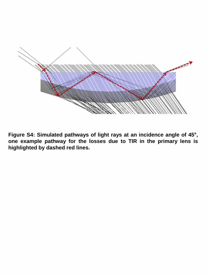
Figure S4: Simulated pathways of light rays at an incidence angle of 45°,
one example pathway for the losses due to TIR in the primary lens is
highlighted by dashed red lines.
0 1 2 3 40.5
0.6
0.7
0.8
0.9
1.0
0.005
0.010
0.015
0.020
0.025Diffuse (w/o Fresnel loss)
RMSD of irradiance
Diffuse (w/ Fresnel loss)
0 20 40 60 80 100
0.0
0.2
0.4
0.6
0.8
1.0
w/o Fresnel loss
w/ Fresnel loss
Incident angle (degree)
Tra
nsm
itta
nce
A
C
f/4 f/3.5 f/3 f/2.5 f/2 f/1.5
f/1 f/0.9 f/0.8 f/0.75 f/0.625 f/0.5
Tra
ns
mit
tan
ce
f/#
RM
SD
B
0.500.520.540.560.580.600.620.640.660.680.700.720.740.760.780.80
Figure S5: Simulation results for transmittance, irradiance uniformity and
irradiance distribution associated with passage of diffuse light (Lambertian)
through outward-facing plano-convex lens arrays, similar to the type used
in CPV+-LP systems. (A) Simulated averaged transmittance of the lens array
as a function of the incident angle of light measured relative to the normal
direction. (B) Dependence of the transmittance of diffuse/direct sunlight
and diffuse irradiance uniformity on the f/# (focal length divided by lens
diameter). The calculations involve ray tracing at a wavelength of 550 nm
for the case of an infinite lens array, with the lens profile optimized as conic
surfaces for convergent focal points. (C) Normalized irradiance distribution
under an infinite lens array for different f/#, with a sampling area equivalent
to that of a single lens unit: higher f/# leads to a higher irradiance
uniformity.
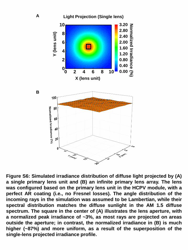
A
Figure S6: Simulated irradiance distribution of diffuse light projected by (A)
a single primary lens unit and (B) an infinite primary lens array. The lens
was configured based on the primary lens unit in the HCPV module, with a
perfect AR coating (i.e., no Fresnel losses). The angle distribution of the
incoming rays in the simulation was assumed to be Lambertian, while their
spectral distribution matches the diffuse sunlight in the AM 1.5 diffuse
spectrum. The square in the center of (A) illustrates the lens aperture, with
a normalized peak irradiance of ~3%, as most rays are projected on areas
outside the aperture; in contrast, the normalized irradiance in (B) is much
higher (~87%) and more uniform, as a result of the superposition of the
single-lens projected irradiance profile.
0 2 4 6 8 100
2
4
6
8
10
0.00
0.40
0.80
1.20
1.60
2.00
2.40
2.80
3.20
X (lens unit)
Light Projection (Single lens)
Y (
len
s u
nit
) N
orm
aliz
ed
Irrad
ian
ce
(%)
B
0 20 40 60 80 1000.0
0.2
0.4
0.6
0.8
1.0
CPV (Direct)
Si (Diffuse)
Voltage (V)
Cu
rre
nt
(A)
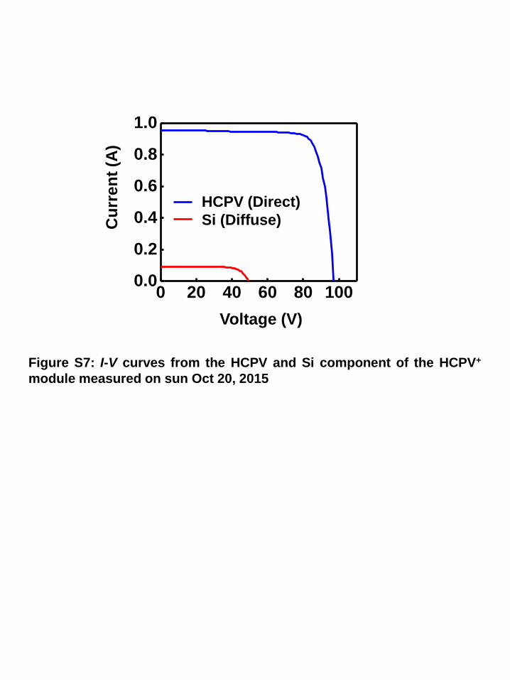
Figure S7: I-V curves from the HCPV and Si component of the HCPV+
module measured on sun Oct 20, 2015
HCPV (Direct)
Si (Diffuse)
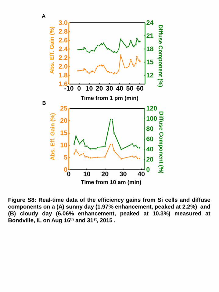
Figure S8: Real-time data of the efficiency gains from Si cells and diffuse
components on a (A) sunny day (1.97% enhancement, peaked at 2.2%) and
(B) cloudy day (6.06% enhancement, peaked at 10.3%) measured at
Bondville, IL on Aug 16th and 31st, 2015 .
A
B
-10 0 10 20 30 40 50 601.6
1.8
2.0
2.2
2.4
2.6
2.8
3.0
12
15
18
21
24
0 10 20 30 400
5
10
15
20
25
0
20
40
60
80
100
120
Ab
s.
Eff
. G
ain
(%
) D
iffus
e C
om
po
ne
nt (%
) A
bs
. E
ff. G
ain
(%
) D
iffuse C
om
po
nen
t (%)
Time from 1 pm (min)
Time from 10 am (min)
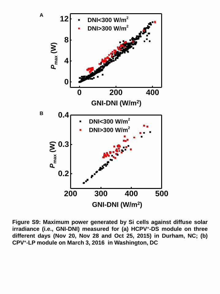
Figure S9: Maximum power generated by Si cells against diffuse solar
irradiance (i.e., GNI-DNI) measured for (a) HCPV+-DS module on three
different days (Nov 20, Nov 28 and Oct 25, 2015) in Durham, NC; (b)
CPV+-LP module on March 3, 2016 in Washington, DC
0 200 400
0
4
8
12 DNI<300 W/m2
DNI>300 W/m2
GNI-DNI (W/m2)
Pm
ax (
W)
200 300 400 500
0.2
0.3
0.4
DNI<300 W/m2
DNI>300 W/m2
GNI-DNI (W/m2)
Pm
ax (
W)
A
B
Photon Energy
/Bandgap (eV)
Eff
icie
nc
y (
%)
Ph
oto
n F
lux (
m-2
eV
-1)
0 1 2 3 40
5
10
15
20 Tracking
Standard
0.0
1.0x10²⁰
2.0x10²⁰
3.0x10²⁰
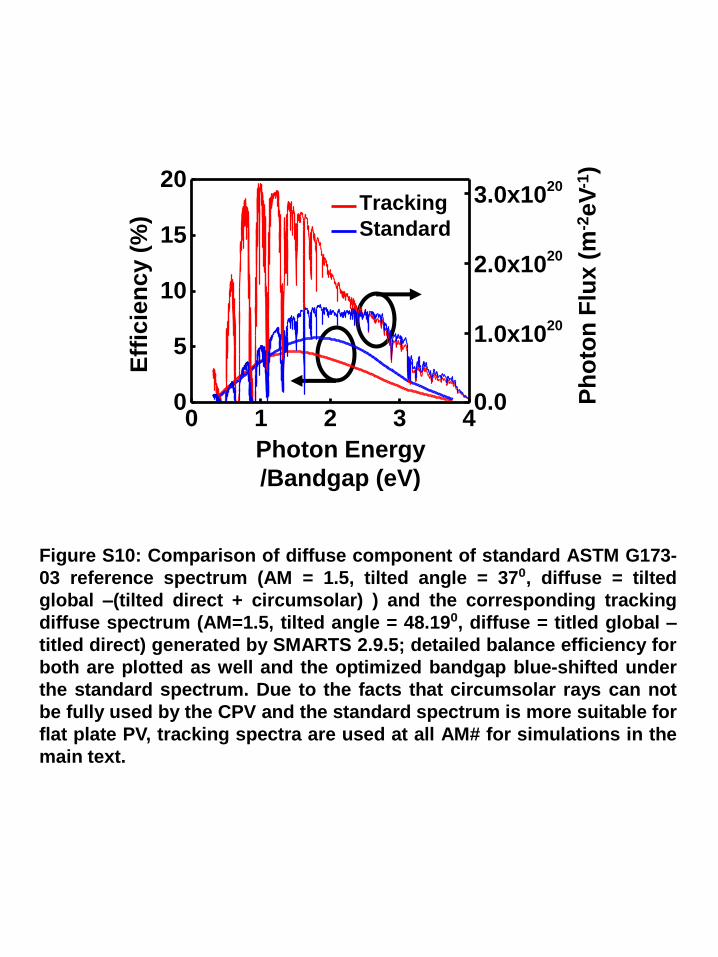
Figure S10: Comparison of diffuse component of standard ASTM G173-
03 reference spectrum (AM = 1.5, tilted angle = 37⁰, diffuse = tilted
global –(tilted direct + circumsolar) ) and the corresponding tracking
diffuse spectrum (AM=1.5, tilted angle = 48.19⁰, diffuse = titled global –
titled direct) generated by SMARTS 2.9.5; detailed balance efficiency for
both are plotted as well and the optimized bandgap blue-shifted under
the standard spectrum. Due to the facts that circumsolar rays can not
be fully used by the CPV and the standard spectrum is more suitable for
flat plate PV, tracking spectra are used at all AM# for simulations in the
main text.
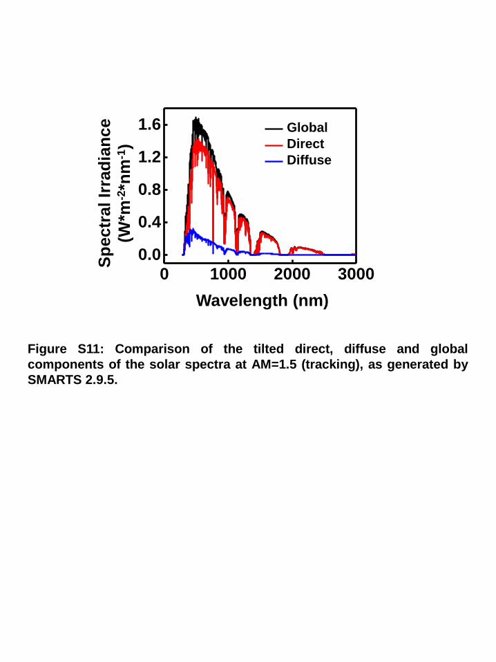
Figure S11: Comparison of the tilted direct, diffuse and global
components of the solar spectra at AM=1.5 (tracking), as generated by
SMARTS 2.9.5.
0 1000 2000 3000
0.0
0.4
0.8
1.2
1.6 Global
Direct
Diffuse
Wavelength (nm)
Sp
ectr
al Ir
rad
ian
ce
(W*m
-2*n
m-1
)


![Photovoltaic Systems with and without Radiation Concentrators … · 2018. 2. 11. · and floor plan area used for each prototype of 1.04 m2 [17]. The concentrator model ... 12%](https://img.pdfslide.us/doc/110x75/5fdddc7d14c5e9338312eb34/photovoltaic-systems-with-and-without-radiation-concentrators-2018-2-11-and.jpg)