Embed Size (px)
Citation preview
GATE CS Topic wise QuestionsComputer Organization and Architecture
www.gatehelp.com
YEAR 2001
Question. 1
More than one word are put in one cache block to
(A) Exploit the temporal locality of reference in a program
(B) Exploit the spatial locality of reference in a program
(C) Reduce the miss penalty
(D) None of the above
SOLUTION
Cache is the small memory which has a very less access time. So it is used for temporal locality of reference whereas virtual memory is for spatial locality of reference.Hence (A) is correct option.
Question. 2
A low memory can be connected to 8085 by using
(A) INTER (B) RESET IN
(C) HOLD (D) READY
SOLUTION
A low memory can be connected to 8085 by using READY signal. If READY is set then communication is possible.
Page 2
www.gatehelp.comCS Topicwise 2001-2010
Computer Organization & Architecture
Hence (D) is correct option.
Question. 3
Suppose a processor does not have any stack pointer register. Which of the following statements is true ?
(A) It cannot have subroutine call instruction
(B) It can have subroutine call instruction, but no nested subroutine calls.
(C) Nested subroutine calls are possible, but interrupts are not.
(D) All sequences of subroutine calls and also interrupts are possible
SOLUTION
Stack pointer register holds the address of top of stack, which is the location of memory at which the CPU should resume its execution after servicing some interrupt or subroutine call.So if SP register not available then no subroutine call instructions are possible.Hence (A) is correct option.
Question. 4
A processor needs software interrupt to
(A) Test the interrupt system of the processor.
(B) Implement co-routines.
(C) Obtain system services which need execution of privileged instructions.
(D) Return from subroutine.
SOLUTION
A CPU needs software interrupt to obtain system services which need execution of privileged instructions.Hence (C) is correct opton.
Question. 5
A CPU has two modes-privileged and non-privileged. In order to change the mode from privileged to non-privileged.
(A) A hardware interrupt is needed.
Page 3
www.gatehelp.comCS Topicwise 2001-2010Computer Organization & Architecture
(B) A software interrupt is needed.
(C) A privileged instruction (which does not generate an interrupt) is needed.
(D) A non-privileged instruction (Which does not generate an interrupt) is needed.
SOLUTION
A software interrupt is initiated by some program module which need some CPU services, at that time the two modes can be interchanged.Hence (B) is correct option.
Question. 6
The process of assigning load addresses to the various parts of the program and adjusting the code and date in the program to reflect the assigned addresses is called
(A) Assembly (B) Parsing
(C) Relocation (D) Symbol resolution
SOLUTION
Load addresses are assigned to various parts of the program, the program can be loaded at any location in memory. This location is added to all addresses in the code, to get correct references.This makes a code re-locatable.Hence (C) is correct option.
Question. 7
Which of the following requires a device driver ?
(A) Register (B) Cache
(C) Main memory (D) Disk
SOLUTION
Device driver is the program which co-ordinates with CPU to regulate the devices. Register, cache & main memory are directly connected to CPU.So only Disk from given options require device drivers.Hence (D) is correct option.
Page 4
www.gatehelp.comCS Topicwise 2001-2010
Computer Organization & Architecture
Question. 8
Which is the most appropriate match for the items in the first column with the items in the second column
(X.) Indirect Addressing (I.) Array implementation
(Y.) Indexed Addressing (II.) Writing re-locatable code
(Z.) Base Register Addressing (III.) Passing array as parameter
(A) (X, III) (Y, I) (Z, II) (B) (X, II) (Y, III) (Z, I)
(C) (X, III) (Y, II) (Z, I) (D) (X, I) (Y, III) (Z, II)
SOLUTION
Indexed addressing is used for array implementation where each element has indexes. Base register is used to re-locatable code, where starts from base address & then all local addresses as added to base address.Indirect addressing is done when array is passed as parameter only name is passed.Hence (A) is correct option.
Question. 9
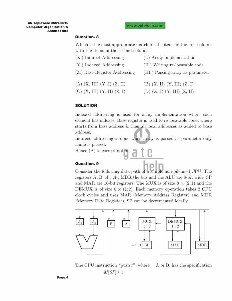
Consider the following data path of a simple non-pilelined CPU. The registers A, B, A1, A2, MDR the bus and the ALU are 8-bit wide. SP and MAR are 16-bit registers. The MUX is of size ( : )8 2 1# and the DEMUX is of size ( : )8 1 2# . Each memory operation takes 2 CPU clock cycles and uses MAR (Memory Address Register) and MDR (Memory Date Register). SP can be decremented locally.
The CPU instruction “push r”, where = A or B, has the specification
[ ]M SP !r
Page 5
www.gatehelp.comCS Topicwise 2001-2010Computer Organization & Architecture
SP SP 1! −
How many CPU clock cycles are needed to execute the “push r” instruction ?
(A) 2 (B) 3
(C) 4 (D) 5
SOLUTION
Push ‘r’Consist of following operations [ ]M SP !r SP SP 1! −‘r’ is stored at memory at address stack pointer currently is, this take 2 clock cycles.SP is then decremented to point to next top of stack. So total cycles 3=Hence (B) is correct option.
Question. 10
Which of the following does not interrupt a running process ?
(A) A device (B) Timer
(C) Scheduler process (D) Power failure
SOLUTION
A device can request interrupt service. A timer when finishes or power failure causes a running process to stop. But a scheduler process doesn’t do this.Hence (C) is correct option.
YEAR 2002
Question. 11
A device employing INTR line for device interrupt puts the CALL instruction on the data bus while
(A) INTA is active (B) HOLD is active
(C) READY is active (D) None of the above
Page 6
www.gatehelp.comCS Topicwise 2001-2010
Computer Organization & Architecture
SOLUTION
INTR is a signal which if enabled then microprocessor has interrupt enabled it receives high INR signal & activates INTA signal, so another request can’t be accepted till CPU is busy in servicing interrupt.Hence (A) is correct option.
Question. 12
In 8085 which of the following modifies the program counter ?
(A) Only PCHL instruction
(B) Only ADD instructions
(C) Only JMP and CALL instructions
(D) All instructions
SOLUTION
Program counter is the register which has the next location of the program to be executed next. JMP & CALL changes the value of PC.PCHL instruction copies content of registers H & L to PC.ADD instruction after completion increments program counter. So program counter is modified in all cases.Hence (D) is correct option.
Question. 13
In serial data transmission, every byte of data is padded with a ‘0’ in the beginning and one or two ‘1’s at the end of byte because
(A) Receiver is to be synchronized for byte reception
(B) Receiver recovers lost ‘0’s and ‘1’ from these padded bits
(C) Padded bits are useful in parity computation.
(D) None of the above
SOLUTION
In serial data transmission the sender & receiver needs to be synchronized with each other. Receiver should know when 1 byte of data has been sent. 0 & 1’s which are padded tell the receiver to synchronize.Hence (A) is correct option.
Page 7
www.gatehelp.comCS Topicwise 2001-2010Computer Organization & Architecture
Question. 14
Which of the following is not a form of memory ?
(A) Instruction cache (B) Instruction register
(C) Instruction opcode (D) Translation-a-side buffer
SOLUTION
Instruction register stores instruction, look-a-side buffer & instruction cache are also memory.But instruction opcodes are the opcodes related to an instruction which are not part of memory hierarchy.Hence (C) is correct option.
Question. 15
In the C language
(A) At most one activation record exists between the current activation record and the activation record for the main.
(B) The number of activation records between the current activation record and the activation record for the main depends on the actual function calling sequence.
(C) The visibility of global variables depends on the actual function calling sequence.
(D) Recursion requires the activation record for the recursive function to be saved on a different stack before the recursive fraction can be called.
SOLUTION
Activation record is the contiguous memory locations where the data needed by the program is kept so at most one activation record exist between current activation record & the record for the main.Hence (A) is correct option.
Question. 16
In the absolute the addressing mode
(A) The operand is inside the instruction
(B) The address of the operand is inside the instruction
(C) The register containing the address of the operand is specified
Page 8
www.gatehelp.comCS Topicwise 2001-2010
Computer Organization & Architecture
inside the instruction
(D) The location of the operand is implicit
SOLUTION
In absolute addressing mode, no need of giving operand, the operand are implicit, instruction itself has knowledge of operands.Hence (D) is correct option.
Question. 17
The performance of a pipelined processor suffers if
(A) The pipelined stages have different delays
(B) Consecutive instructions are dependent on each other
(C) The pipeline stages share hardware resources
(D) All the above
SOLUTION
Pipelining is a method to execute a program breaking it in several independent sequence of stages.In that case pipeline stages can’t have different delays, no dependency among consecutive instructions & sharing of hardware resources shouldn’t be there. So option (D) is trueHence (D) is correct option.
Question. 18
Horizontal microprogramming
(A) Does not require use of signal decoders
(B) Results in larger sized microinstructions than vertical microprogramming
(C) Uses one bit for each control signal
(D) All of the above
SOLUTION
In horizontal microprogramming the instruction size is not large, & no decoding is required. But 1 bit is used for all control signals.Hence (C) is correct option.
Page 9
www.gatehelp.comCS Topicwise 2001-2010Computer Organization & Architecture
YEAR 2003
Question. 19
For a pipelined CPU with a single ALU, consider the following situations
1. The j st1+ − instruction uses the result of j th− instruction as an operand
2. The execution of a conditional jump instruction
3. The j th− and j st1+ − instructions require the ALU at the same time
Which of the above can cause a hazard?
(A) 1 and 2 only (B) 2 and 3 only
(C) 3 only (D) All the three
SOLUTION
Case 1 is here of data dependency, this can’t be safe with single ALU so read after write.
Case 2 Conditional jumps are always hazardous they create conditional dependency in pipeline
Case 3 This is write after read problem or concurrency dependency so hazardous
All the three are hazardous.Hence (D) is correct option.
Question. 20
Consider an array multiplier for multiplying two n bit numbers. If each gate in the circuit has a unit delay, the total delay of the multiplier is
(A) ( )1Θ (B) ( )lognΘ
(C) ( )nΘ (D) ( )n2Θ
SOLUTION
The no. of gates used in n bit array multiplier ( )n n# is n2 1− . So. if every single gate takes unit delay, then total delay 0(2 1) ( )n n0− =It is of linear orderHence (C) is correct option.
Page 10
www.gatehelp.comCS Topicwise 2001-2010
Computer Organization & Architecture
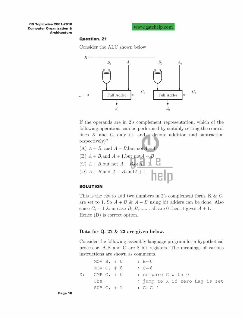
Question. 21
Consider the ALU shown below
If the operands are in 2’s complement representation, which of the following operations can be performed by suitably setting the control lines K and C0 only (+ and - denote addition and subtraction respectively)?
(A) ,A B+ and ,A B− but not 1A +
(B) ,A B+ and 1,A + but notA B−
(C) ,A B+ but not ,A B− or 1A +
(D) ,A B+ and ,A B− and 1A +
SOLUTION
This is the ckt to add two numbers in 2’s complement form. K & C0 are set to 1. So A B+ & A B− using bit adders can be done. Also since C 10 = & in case , ........B B0 1 all are 0 then it gives A 1+ .Hence (D) is correct option.
Data for Q. 22 & 23 are given below.
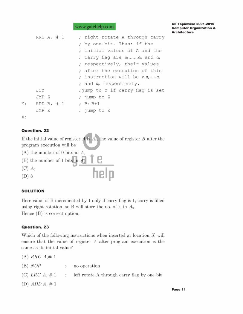
Consider the following assembly language program for a hypothetical processor. A,B and C are 8 bit registers. The meanings of various instructions are shown as comments.
MOV B, # 0 ; B!0 MOV C, # 8 ; C!8Z: CMP C, # 0 ; compare C with 0 JZX ; jump to X if zero fl ag is set SUB C, # 1 ; C!C−1
Page 11
www.gatehelp.comCS Topicwise 2001-2010Computer Organization & Architecture
RRC A, # 1 ; right rotate A through carry ; by one bit. Thus: if the ; initial values of A and the ; carry fl ag are .......a a7 0 and c0
; respectively, their values ; after the execution of this ; instruction will be .....c a a0 7 1
; and a0 respectively. JCY ;jump to Y if carry fl ag is set JMP Z ; jump to ZY: ADD B, # 1 ; B!B+1 JMP Z ; jump to ZX:
Question. 22
If the initial value of register A is A0, the value of register B after the program execution will be
(A) the number of 0 bits in A0
(B) the number of 1 bits in A0
(C) A0
(D) 8
SOLUTION
Here value of B incremented by 1 only if carry flag is 1, carry is filled using right rotation, so B will store the no. of is in A0.Hence (B) is correct option.
Question. 23
Which of the following instructions when inserted at location X will ensure that the value of register A after program execution is the same as its initial value?
(A) ,#RRC A 1
(B) NOP ; no operation
(C) , #LRC A 1 ; left rotate A through carry flag by one bit
(D) , # 1ADD A
Page 12
www.gatehelp.comCS Topicwise 2001-2010
Computer Organization & Architecture
SOLUTION
In the end of program execution to check whether both initial and final value of register A is A0, we need to right rotate register A through carry by one bit.Hence (A) is correct option.
YEAR 2004
Question. 24
Which of the following addressing modes are suitable for program relocation at run time?
1. Absolute addressing
2. Based addressing
3. Relative addressing
4. Indirect addressing
(A) 1 and 4 (B) 1 and 2
(C) 2 and 3 (D) 1,2 and 4
SOLUTION
Program relocation at run time transfers complete block to some memory locations. This require as base address and block should be relatively addressed through this base address.This require both based addressing and relative addressing mode.Hence (C) is correct option.
Question. 25
Consider a multiplexer with X and Y as data inputs and Z as control input.Z 0= selects input X , and Z =1 selects input Y . What are the connection required to realize the 2-variable Boolean function f T R= + , without using any additional hardware?
(A) R to X, 1 to Y, T to Z (B) T to X, R to Y, T to Z
(C) T to X, R to Y, 0 to Z (D) R to X, 0 to Y, T to Z
Page 13
www.gatehelp.comCS Topicwise 2001-2010Computer Organization & Architecture
SOLUTION
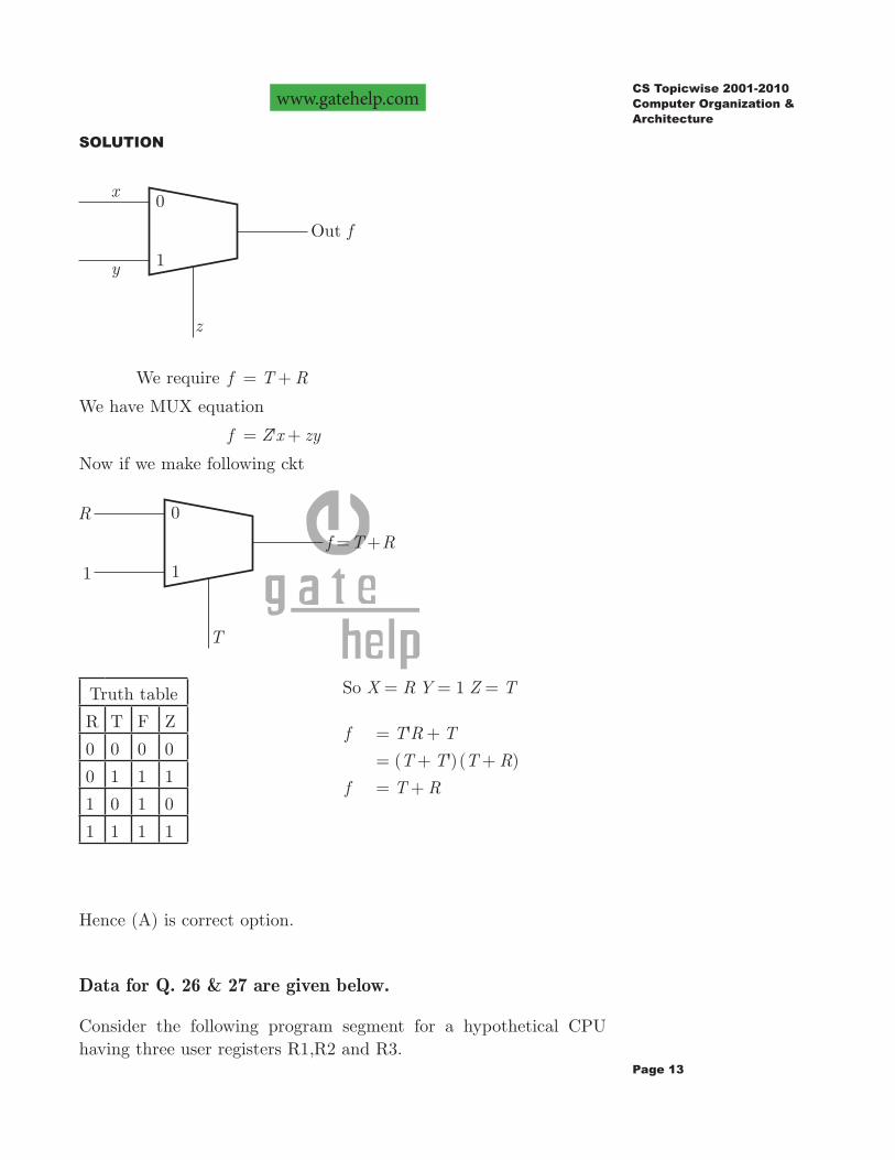
We require f T R= +
We have MUX equation
f 'Z x zy= +
Now if we make following ckt
Truth table
R T F Z
0 0 0 0
0 1 1 1
1 0 1 0
1 1 1 1
So X R= Y 1= Z T=
f 'T R T= +
( ')( )T T T R= + +
f T R= +
Hence (A) is correct option.
Data for Q. 26 & 27 are given below.
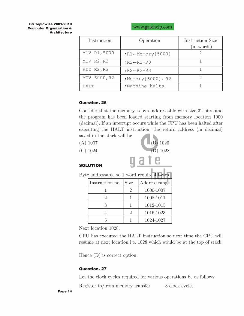
Consider the following program segment for a hypothetical CPU having three user registers R1,R2 and R3.
Page 14
www.gatehelp.comCS Topicwise 2001-2010
Computer Organization & Architecture
Instruction Operation Instruction Size (in words)
MOV R1,5000 ;R1!Memory[5000] 2
MOV R2,R3 ;R2!R2+R3 1
ADD R2,R3 ;R2!R2+R3 1
MOV 6000,R2 ;Memory[6000]!R2 2
HALT ;Machine halts 1
Question. 26
Consider that the memory is byte addressable with size 32 bits, and the program has been loaded starting from memory location 1000 (decimal). If an interrupt occurs while the CPU has been halted after executing the HALT instruction, the return address (in decimal) saved in the stack will be
(A) 1007 (B) 1020
(C) 1024 (D) 1028
SOLUTION
Byte addressable so 1 word require 4 bytes.
Instruction no. Size Address range
1 2 1000-1007
2 1 1008-1011
3 1 1012-1015
4 2 1016-1023
5 1 1024-1027
Next location 1028.
CPU has executed the HALT instruction so next time the CPU will resume at next location i.e. 1028 which would be at the top of stack.
Hence (D) is correct option.
Question. 27
Let the clock cycles required for various operations be as follows:
Register to/from memory transfer: 3 clock cycles
Page 15
www.gatehelp.comCS Topicwise 2001-2010Computer Organization & Architecture
ADD with both operands in register: 1 clock cycle
Instruction fetch and decode: 2 clock cycles per word
The total number of clock cycles required to execute the program is
(A) 29 (B) 24
(C) 23 (D) 20
SOLUTION
The clock cycles are per block so if an instruction size is 2 then it requires twice no. of clock cycles.
Instruction No. Size No. of clock cycles
1 2 3 2 2# + 8
2 1 1 3 2# + 5
3 1 1(add only) 1
4 2 3 2 2# + 8
5 1 2(fetch & decode) 2
Total 24
Hence (B) is correct option.
Question. 28
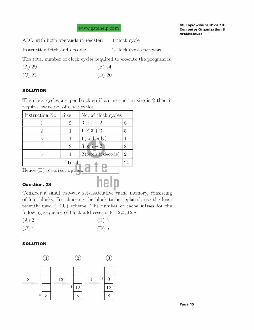
Consider a small two-way set-associative cache memory, consisting of four blocks. For choosing the block to be replaced, use the least recently used (LRU) scheme. The number of cache misses for the following sequence of block addresses is 8, 12,0, 12,8
(A) 2 (B) 3
(C) 4 (D) 5
SOLUTION
Page 16
www.gatehelp.comCS Topicwise 2001-2010
Computer Organization & Architecture
After than 12 & 8 are referred but this does not cause any miss So no. of miss 3=This stars ( )) shows the misses.Hence (B) is correct option.
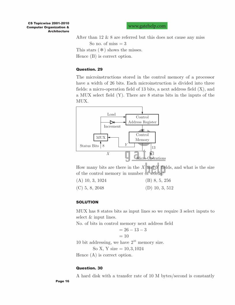
Question. 29
The microinstructions stored in the control memory of a processor have a width of 26 bits. Each microinstruction is divided into three fields: a micro-operation field of 13 bits, a next address field (X), and a MUX select field (Y). There are 8 status bits in the inputs of the MUX.
How many bits are there in the X and Y fields, and what is the size of the control memory in number of words?
(A) 10, 3, 1024 (B) 8, 5, 256
(C) 5, 8, 2048 (D) 10, 3, 512
SOLUTION
MUX has 8 states bits as input lines so we require 3 select inputs to select & input lines.No. of bits in control memory next address field 26 13 3= − − 10=10 bit addressing, we have 210 memory size. So X, Y size , ,10 3 1024=Hence (A) is correct option.
Question. 30
A hard disk with a transfer rate of 10 M bytes/second is constantly
Page 17
www.gatehelp.comCS Topicwise 2001-2010Computer Organization & Architecture
transferring data to memory using DMA. The processor runs at 600 MHz. and takes 300 and 900 clock cycles to initiate and complete DMA transfer respectively. If the size of the transfer is 20 Kbytes, what is the percentage of processor time consumed for the transfer operation?
(A) 5.0% (B) 1.0%
(C) 0.5% (D) 0.1%
SOLUTION
Transfer rate 10= MB ps Data 20= KB
Time 10 220 2 2 1020
103
#
##= = −
2= ms Processor speed 600= MHz 600= cycles/sec. Cycles required by CPU 300 900= + For DMA 1200=
So time .600 10
1200 0026#
= = ms
% .2
002 100#=
. %0 1=Hence (D) is correct.
Question. 31
A 4-stage pipeline has the stage delays as 150, 120, 160 and 140 nanoseconds respectively. Registers that are used between the stages have a delay of 5 nanoseconds each. Assuming constant clocking rate, the total time taken to process 1000 data items on this pipeline will be
(A) 120.4 microseconds (B) 160.5 microseconds
(C) 165.5 microseconds (D) 590.0 microseconds
SOLUTION
Delay 5= ns/stageTotal delay in pipline.
Page 18
www.gatehelp.comCS Topicwise 2001-2010
Computer Organization & Architecture
150 120 160 140 570= + + + =Delay due to 4 stages.Stage 1 delay 1 stage 2 delay 2 stage 3 stage 4 5 3# 15= Total 570 15 585= + =
Total time 585 ns1000 data items=
.165 5= microseconds.Hence (C) is correct option
YEAR 2005
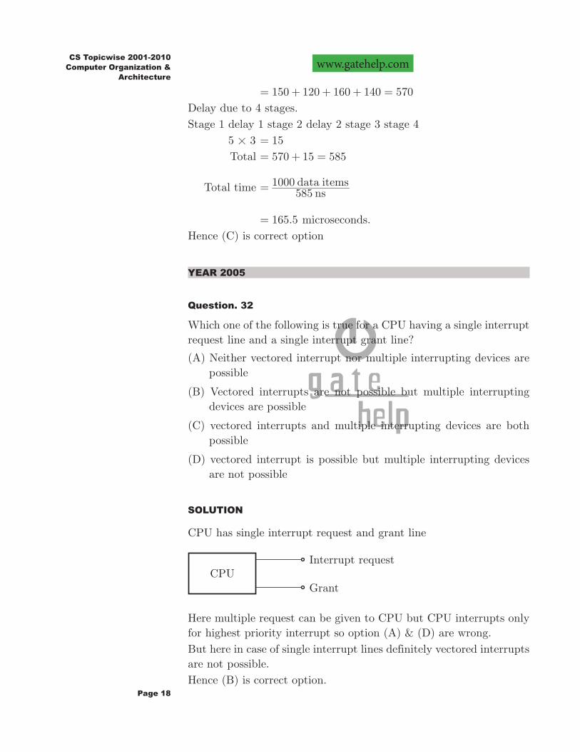
Question. 32
Which one of the following is true for a CPU having a single interrupt request line and a single interrupt grant line?
(A) Neither vectored interrupt nor multiple interrupting devices are possible
(B) Vectored interrupts are not possible but multiple interrupting devices are possible
(C) vectored interrupts and multiple interrupting devices are both possible
(D) vectored interrupt is possible but multiple interrupting devices are not possible
SOLUTION
CPU has single interrupt request and grant line
Here multiple request can be given to CPU but CPU interrupts only for highest priority interrupt so option (A) & (D) are wrong.But here in case of single interrupt lines definitely vectored interrupts are not possible.Hence (B) is correct option.
Page 19
www.gatehelp.comCS Topicwise 2001-2010Computer Organization & Architecture
Question. 33
Normally user programs are prevented from handing I/O directly by I/O instructions in them. For CPUs having explicit I/O instructions, such I/O protection is ensured by having the I/O instructions privileged. In a CPU with memory mapped I/O, there is no explicit I/O instruction. Which one of the following is true for a CPU with memory mapped I/O?
(A) I/O protection is ensured by operating system routine(s)
(B) I/O protection is ensured by a hardware trap
(C) I/O protection is ensured during system configuration
(D) I/O protection is not possible
SOLUTION
In memory mapped I/0 the complete system (memory + I/0 ports) hold the same set of addresses. They are considered to be the part of that memory only. This management is done by OS only.Hence (A) is correct option.
Question. 34
What is the swap apace in the disk used for?
(A) Saving temporary html pages
(B) Saving process data
(C) Storing the super-block
(D) Storing device drivers
SOLUTION
Swap space is the memory pre allowed to store process’s data. This can be compared with virtual memory. The data required to complete process is kept here.Hence (B) is correct option.
Question. 35
Increasing the RAM of a computer typically improves performance because
(A) Virtual memory increases
(B) Larger RAMs are faster
Page 20
www.gatehelp.comCS Topicwise 2001-2010
Computer Organization & Architecture
(C) Fewer page faults occur
(D) Fewer segmentation faults occur
SOLUTION
Due to increase in RAM size all the pages required by CPU are available in RAM so page fault chance are less, so virtual memory access chances are less and latency is reduced for secondary memory.Hence (C) is correct option.
Question. 36
Consider a three word machine instruction
[ ],@ADD A R B0
The first operand (destination) “ [ ]A R0 ” uses indexed addressing mode with R0 as the index register. The second operand (source) "@ "B uses indirect addressing mode. A and B are memory addresses residing at the second and the third words, respectively. The first word of the instruction specifies the opcode, the index register designation and the source and destination addressing modes. During execution of ADD instruction, the two operands are added and stored in the destination (first operand).
The number of memory cycles needed during the execution cycle of the instruction is
(A) 3 (B) 4
(C) 5 (D) 6
SOLUTION
ADD [ ],@A R B0
This is instruction has 3 computational parts. ADD instruction requires 1 machine cycle, [ ]A R0 here R0 is index register which has starting address of index then this index has the block address. This whole operation require 3 machine cycles. Now @ B is indirect addressing. This takes 2 machine cycles. So overall 1 3 2 6+ + = machine cycles.Hence (D) is correct option.
Page 21
www.gatehelp.comCS Topicwise 2001-2010Computer Organization & Architecture
Question. 37
Match List-I with List-II and select the correct answer using the codes given below the lists:
List-I List-II
A. [ ] [ ];A B j1 = 1. Indirect addressing
B. while [* ]A ++ ; 2. Indexed addressing
C. int temp=*x ; 3. Auto increment
Codes:
A B C
(A) 3 2 1
(B) 1 3 2
(C) 2 3 1
(D) 1 2 3
SOLUTION
LIST-IA. [ ] [ ];A B J1 =
B. While [ ]A) ++
C. int temp X)=
LIST-II2 Indexed addressing here the
indexing is used
3. Auto increment the memory locations is A are automatically incriminated.
1. Indirect addressing here temp is assigned the value of int type stored at the address contained in X
A2 B3 C1Hence (C) is correct option.
Question. 38
Consider a direct mapped cache of size 32 KB with block size 32 bytes. The CPU generates 32 bit addresses. The number of bits needed for cache indexing and the number of tag bits are respectively
(A) 10,17 (B) 10,22
Page 22
www.gatehelp.comCS Topicwise 2001-2010
Computer Organization & Architecture
(C) 15,17 (D) 5,17
SOLUTION
Cache is direct mapped. Size of Cache 32= KB 2 25 10
#= B 215= Bytes.Require 15 bits for cache addressing so CPU address has tag and index No. of tag bits 32 15= − 17=From 15 Cache addressing bits consist of blocks & words. Each block has 32 words (bytes) So require 5 bit. Index block word= + Block 15 5= − 10=
So, 10, 17Hence (A) is correct option.
Question. 39
A 5 stage pipelined CPU has the following sequence of stages
IF-Instruction fetch from instruction memory.
RD-Instruction decode and register read,
EX- Execute:ALU operation for data and address computation,
MA-Data memory access-for write access the register read at
RD stage it used,
WB-register write back.
Consider the following sequence of instruction:
: 0,Locl;I LR1 0 [Locl]R M<= 0, 0;I AR R2 0 0 0R R R<= + 2, 0;I AR R3 2 2 0R R R<= −
Let each stage take one clock cycle.
What is the number of clock cycles taken to complete the above sequence of instruction starting from the fetch of I1?
Page 23
www.gatehelp.comCS Topicwise 2001-2010Computer Organization & Architecture
(A) 8 (B) 10
(C) 12 (D) 15
SOLUTION
Order of phase in instruction cycle.IF A E MA WB" " "3 #
1 2 3 4 5 6 7 8 9 10
[ ]R M LOC0 ! IF RD EX MA WB
R R R0 0 0! + IF RD EX MA WB
R R R2 2 0! − IF RD EX MA WB
R R R0 0 0! + can’t start before 3 since R0 has not been read by I1.
R R R2 2 0! − can’t start before 6th since I2 has not executed R R R0 0 0! + till 5th cycle
Total cycles 10=Hence (B) is correct option.
Question. 40
A device with data transfer rate 10 KB/sec is connected to a CPU. Data is transferred byte-wise. Let the interrupt overhead be 4 secμ .
The byte transfer time between the device interface register and CPU or memory is negligible. What is the minimum performance gain of operating the device under interrupt mode over operating it under program controlled mode?
(A) 15 (B) 25
(C) 35 (D) 45
SOLUTION
Data transfer rate 10000= B/sec Total data 25 103
#= Rate 104=
Performance gain 1025 1004 #=
%25=
Page 24
www.gatehelp.comCS Topicwise 2001-2010
Computer Organization & Architecture
Hence (B) is correct option.
Question. 41
Consider a disk drive with the following specification
16 surfaces, 512 tracks/surface, 512 sectors/track, 1 KB/sector, rotation speed 3000 .rpm The disk is operated in cycle stealing mode whereby whenever one byte word is ready it is sent to memory; similarly, for writing, the disk interface reads a 4 byte word from the memory in each DMA cycle. Memory cycle time is 40 secn . The maximum percentage of time that the CPU gets blocked during DMA operation is
(A) 10 (B) 25
(C) 40 (D) 50
SOLUTION
Disk revolutions 3000= PM or 50 RPS
At a time can read in
One revolution 512= KB
Tracks read/sec 22 502
19
)=
50 217#= per sec.
Interrupt .2621= sec
Percentage gain .1
2621 100#=
%26,
Hence (B) is correct option.
Data for Q. 42 & 43 are given below
Consider the following data path of a CPU
Page 25
www.gatehelp.comCS Topicwise 2001-2010Computer Organization & Architecture
The, ALU, the bus and all the registers in the data path are of identical size. All operations including incrementation of the PC and the GPRs are to be carried out in the ALU. Two clock cycle are needed for memory read operation-the first one for loading data from the memory but into the MDR.
Question. 42
The instruction “add ,R R0 1” has the register transfer in terpretation R R R0 0 1<= + . The minimum number of clock cycles needed for execution cycle of this instruction is
(A) 2 (B) 3
(C) 4 (D) 5
SOLUTION
R0 R R0 1! +First cycle require to fetch operands two cycles required for this.The next cycle required to use ALU to perform ADD operation. So total cycles required 3=
Hence (D) is correct option.
Question. 43
The instruction “call Rn , sub” is a two word instruction. Assuming that PC is incremented during the fetch cycle of the first word of the instruction, its register transfer interpretation is
;Rn PC 1<= =
[ ];PC M PC<=
Page 26
www.gatehelp.comCS Topicwise 2001-2010
Computer Organization & Architecture
The minimum number of CPU clock cycles needed during the execution cycle of this instruction is
(A) 2 (B) 3
(C) 4 (D) 5
SOLUTION
Rn PC 1! + PC [ ]M PC=Program outer is itself a register so incremented in 1 cycle.Now fetching the memory at PC & the value of at address stored in PC takes 2 cycles. So total 1 2+ 3= cycles.Hence (B) is correct option.
Question. 44
A CPU has 24-bit instructions. A program starts at address 300(in decimal). Which one of the following is a legal program counter (all values in decimal)?
(A) 400 (B) 500
(C) 600 (D) 700
SOLUTION
Size of instruction 24= bits.
Since each instruction require 324 3= bytes & start address is 300 so
the address for this range can be multiple of 3 only so 600.Hence (C) is correct option.
YEAR 2006
Question. 45
A CPU has a cache with block size 64 bytes. The main memory has k banks, each bank being c bytes wide. Consecutive c -bute chunks are mapped on consecutive banks with warp-around. All the k banks can be accessed in parallel, but two accesses to the same bank must be serialized. A cache block access may involve multiple iterations of parallel bank accesses depending on the amount of data obtained by accessing all the k banks in parallel. Each iteration requires decoding

Page 27
www.gatehelp.comCS Topicwise 2001-2010Computer Organization & Architecture
the bank numbers to be accessed in parallel and this takes /k ns2 . The latency of one bank access is 80 ns . If c 2= and k=24, then latency of retrieving a cache block starting at address zero from main memory is
(A) 92 ns (B) 104 ns
(C) 172 ns (D) 184 ns
SOLUTION
Size of Cache block 64= B No. of main memory banks K 24= Size of each bank C 2= bytes.
So time taken for < access. T decoding time latency time= + T K/2 latency= + 12 80= + 92= ns. But since C 2= for accesses. 2 92# 189= ns.Hence (D) is correct option
Question. 46
A CPU has five-stages pipeline and runs at 1GHz frequency. Instruction fetch happens in the first stage of the pipeline. A conditional branch instruction computes the target address and evaluates the condition in the third stage of the pipeline. The processor stops fetching new instructions following a conditional branch until the branch outcome is known. A program executes 109 instructions out of which 20% are conditional branches. If each instruction takes one cycle to complete on average, then total execution time of the program is
(A) 1.0 second (B) 1.2 seconds
(C) 1.4 seconds (D) 11.6 seconds
SOLUTION
Given that 80% of 109 instruction require single cycle i.e. no conditional branching & for 20% an extra cycle required. Time taken by 1 cycle 10 9= − sec.
Page 28
www.gatehelp.comCS Topicwise 2001-2010
Computer Organization & Architecture
Total time 10 10080 10 100
20 2 109 9 9# # #= +−
b l
10 10 54
529 9
#= +−b l
.56 1 2= = seconds.
Hence (B) is correct option.
Question. 47
Consider a new instruction named branch-on-bit-set (mnemonic bbs). The instruction “bbs reg, pos, labbel” jumps to label if bit in position pos of register operand reg is one. a register is 32 bits wide and the bits are numbered 0 to 31, bit in position 0 being the least significant. Consider the following emulation of this instruction on a processor that does not have bbs implemented.
temp!reg and mask
Branch to label if temp is non-zero
The variable temp is a temporary register. For correct emulation the variable mask must be generated by
(A) mask x pos0 1 <<! (B) musk x ffffffff pos0 >>!
(C) mask pos! (D) msdk xf0!
SOLUTION
Given instructionbbs reg, pos, LabelHere pos bit decided whether to jump to label. So all other bits in temp set to 0. Temp ! reg and mask.So of temp is not zero branch to label.So shifting left over. Mask 0 1 pos<<! #
Hence (D) is correct option.
Data for Q. 48 & Q. 49 are given below. Solve the problem and choose the correct answers.
Consider two cache organizations: The first one is 32 KB 2-way set associative with 32-bytes block size. The second one is of the same
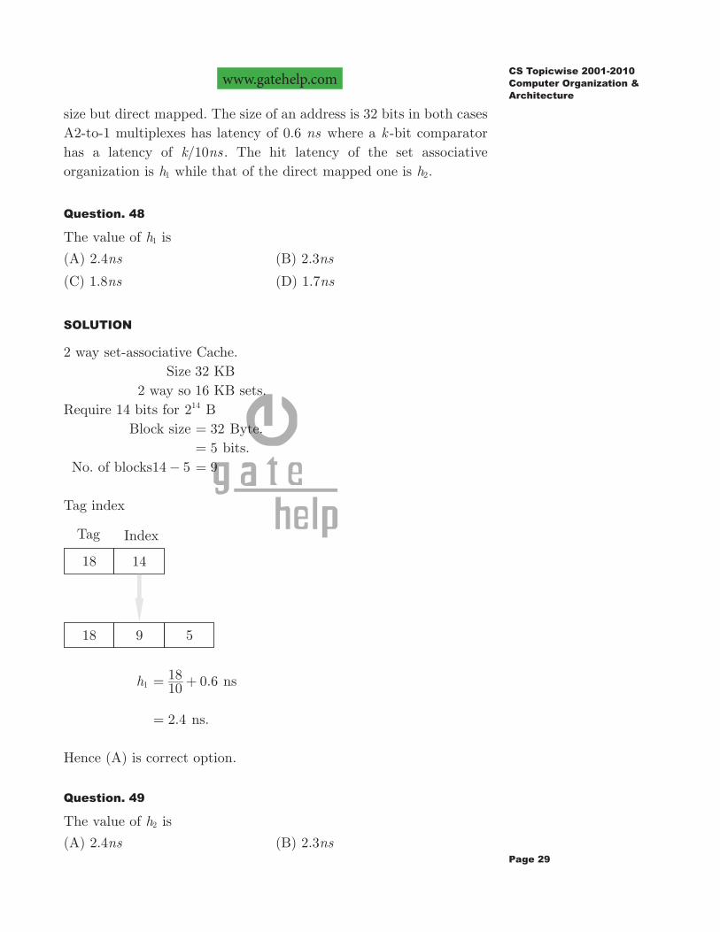
Page 29
www.gatehelp.comCS Topicwise 2001-2010Computer Organization & Architecture
size but direct mapped. The size of an address is 32 bits in both cases A2-to-1 multiplexes has latency of 0.6 ns where a k -bit comparator has a latency of /k ns10 . The hit latency of the set associative organization is h1 while that of the direct mapped one is h2.
Question. 48
The value of h1 is
(A) 2.4ns (B) 2.3ns
(C) 1.8ns (D) 1.7ns
SOLUTION
2 way set-associative Cache. Size 32 KB 2 way so 16 KB sets.Require 14 bits for 214 B Block size 32= Byte. 5= bits. No. of blocks14 5− 9=
Tag index
h1 .1018 0 6= + ns
.2 4= ns.
Hence (A) is correct option.
Question. 49
The value of h2 is
(A) 2.4ns (B) 2.3ns
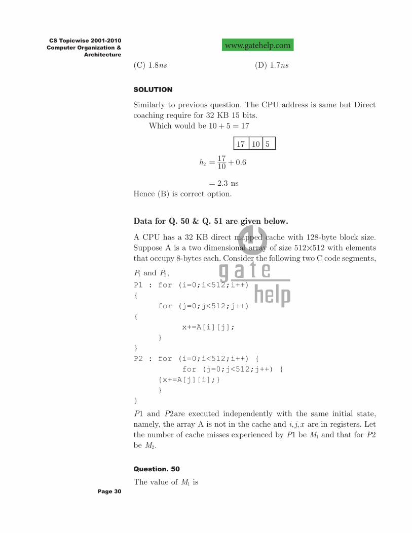
Page 30
www.gatehelp.comCS Topicwise 2001-2010
Computer Organization & Architecture
(C) 1.8ns (D) 1.7ns
SOLUTION
Similarly to previous question. The CPU address is same but Direct coaching require for 32 KB 15 bits. Which would be 10 5 17+ =
17 10 5
h2 .1017 0 6= +
.2 3= nsHence (B) is correct option.
Data for Q. 50 & Q. 51 are given below.
A CPU has a 32 KB direct mapped cache with 128-byte block size. Suppose A is a two dimensional array of size 512#512 with elements that occupy 8-bytes each. Consider the following two C code segments,
P1 and P2,
P1 : for (i=0;i<512;i++){ for (j=0;j<512;j++){ x+=A[i][j]; }}P2 : for (i=0;i<512;i++) { for (j=0;j<512;j++) { {x+=A[j][i];} }}
1P and 2P are executed independently with the same initial state, namely, the array A is not in the cache and , ,i j x are in registers. Let the number of cache misses experienced by P1 be M1 and that for P2 be M2.
Question. 50
The value of M1 is
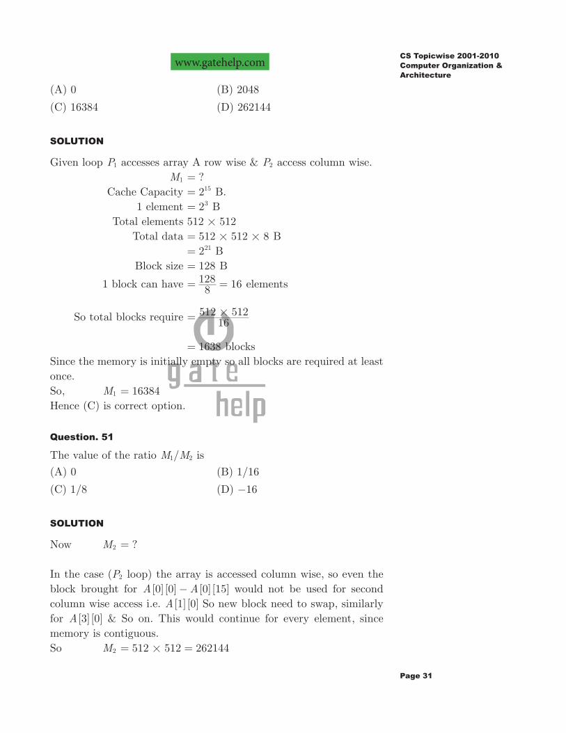
Page 31
www.gatehelp.comCS Topicwise 2001-2010Computer Organization & Architecture
(A) 0 (B) 2048
(C) 16384 (D) 262144
SOLUTION
Given loop P1 accesses array A row wise & P2 access column wise. M1 ?= Cache Capacity 215= B. 1 element 23= B Total elements 512 512#
Total data 512 512 8# #= B 221= B Block size 128= B
1 block can have 8128 16= = elements
So total blocks require 512 51216#=
1638= blocksSince the memory is initially empty so all blocks are required at least once.So, M1 16384=Hence (C) is correct option.
Question. 51
The value of the ratio M1/M2 is
(A) 0 (B) 1/16
(C) 1/8 (D) −16
SOLUTION
Now M2 ?=
In the case (P2 loop) the array is accessed column wise, so even the block brought for [ ] [ ] [ ] [ ]A A0 0 0 15− would not be used for second column wise access i.e. [ ] [ ]A 1 0 So new block need to swap, similarly for [ ] [ ]A 3 0 & So on. This would continue for every element, since memory is contiguous.So M2 512 512 262144#= =
Page 32
www.gatehelp.comCS Topicwise 2001-2010
Computer Organization & Architecture
& MM
2
1 26214416384
161= =
Hence (B) is correct option.
YEAR 2007
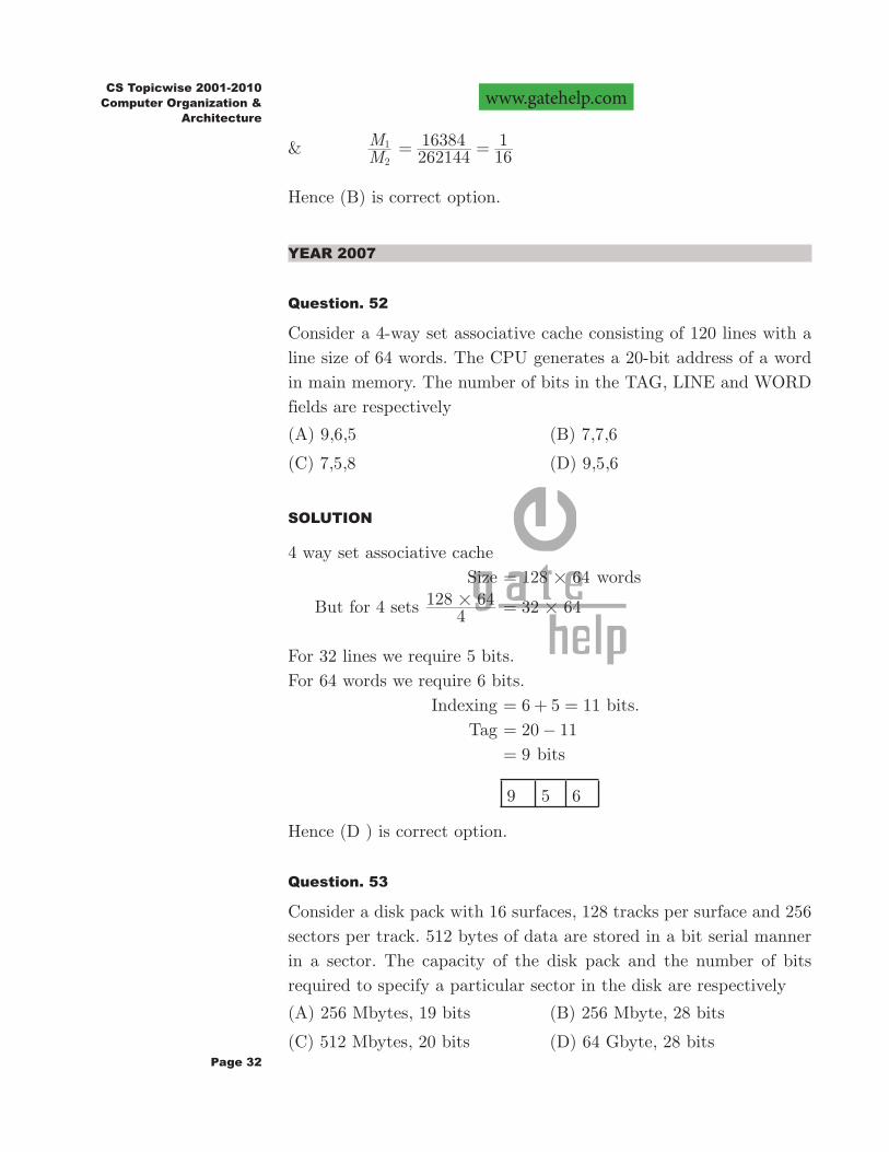
Question. 52
Consider a 4-way set associative cache consisting of 120 lines with a line size of 64 words. The CPU generates a 20-bit address of a word in main memory. The number of bits in the TAG, LINE and WORD fields are respectively
(A) 9,6,5 (B) 7,7,6
(C) 7,5,8 (D) 9,5,6
SOLUTION
4 way set associative cache Size 128 64#= words
But for 4 sets 4128 64# 32 64#=
For 32 lines we require 5 bits.For 64 words we require 6 bits. Indexing 6 5 11= + = bits. Tag 20 11= − 9= bits
9 5 6
Hence (D ) is correct option.
Question. 53
Consider a disk pack with 16 surfaces, 128 tracks per surface and 256 sectors per track. 512 bytes of data are stored in a bit serial manner in a sector. The capacity of the disk pack and the number of bits required to specify a particular sector in the disk are respectively
(A) 256 Mbytes, 19 bits (B) 256 Mbyte, 28 bits
(C) 512 Mbytes, 20 bits (D) 64 Gbyte, 28 bits
Page 33
www.gatehelp.comCS Topicwise 2001-2010Computer Organization & Architecture
SOLUTION
Surface 6= Tracks 16 128#= Sectors 16 128 256# #= 2 2 2 24 7 8 19
# #= =So 19 lines are required to address all sectors. Bytes 2 51219
#= B 2 219 9
#= B 228= 256= MBHence (A) is correct option.
Question. 54
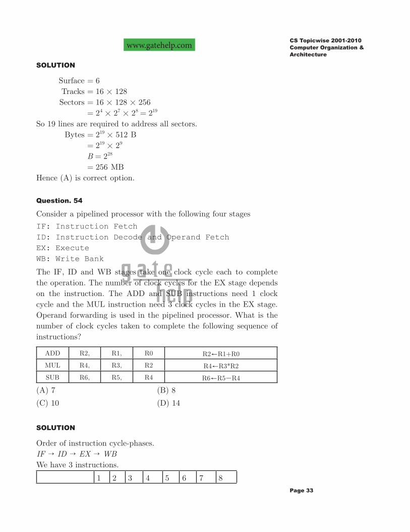
Consider a pipelined processor with the following four stages
IF: Instruction FetchID: Instruction Decode and Operand FetchEX: ExecuteWB: Write Bank
The IF, ID and WB stages take one clock cycle each to complete the operation. The number of clock cycles for the EX stage depends on the instruction. The ADD and SUB instructions need 1 clock cycle and the MUL instruction need 3 clock cycles in the EX stage. Operand forwarding is used in the pipelined processor. What is the number of clock cycles taken to complete the following sequence of instructions?
ADD R2, R1, R0 R2!R1+R0
MUL R4, R3, R2 R4!R3*R2
SUB R6, R5, R4 R6!R5−R4
(A) 7 (B) 8
(C) 10 (D) 14
SOLUTION
Order of instruction cycle-phases.IF ID EX WB" " "
We have 3 instructions.
1 2 3 4 5 6 7 8
Page 34
www.gatehelp.comCS Topicwise 2001-2010
Computer Organization & Architecture
R R R2 1 0! ! IF ID EX WB
R R R4 3 2! ! IF ID EX EX EX WB
R R R6 5 4! ! IF ID - - EX WB
Represent wait in pipeline due to result dependently.
Clock cycles require 8=
Hence (B) is correct option.
Data for Q. 55, 56 & 57 are given below.
Consider the following program segment. Here R1, R2 and R3 are the
general purpose registers.
Instruction Operation Instruction size(no. of words)
MOV R1,(3000) R1!M[3000] 2
LOOP:MOV R2,R1 R2!M[R3] 1
ADD R2,R1 R2!R1+R2 1
MOV (R3),R2 M(R3]!R2 1
INC R3 R3!R3+1 1
DEC R1 R1!R1-1 1
BNZ LOOP Branch on not zero 2HALT Stop
Assume that the content of memory location 3000 is 10 and the
content of the register R3 is 2000. The content of each of the memory
locations from 2000 to 2010 is 100. The program is loaded from the
memory location 100. All the numbers are in decided.
Question. 55
Assume that the memory is word addressable. The number of memory
references for accessing the data in executing the program completely
is
(A) 10 (B) 11
(C) 20 (D) 21
Page 35
www.gatehelp.comCS Topicwise 2001-2010Computer Organization & Architecture
SOLUTION
1st memory reference R M1 ! 3000^ h and then in the loop which runs for 10 times there are 2 memory reference every iteration. 10 2# 20=Total 20 1+ 21= R2 [ ]M R3!
[ ]M R3 R2!
Hence (D) is correct option
Question. 56
Assume that the memory is word addressable. After the execution of this program, the content of memory location 2010 is
(A) 100 (B) 101
(C) 102 (D) 110
SOLUTION
Program stores results from 2000 to 2010. It stores 110, 109, 108......100 at 2010 location.DEC R1Hence (A) is correct option.
Question. 57
Assume that the memory is byte addressable and the word size is 32 bits. If an interrupt occurs during the execution of the instruction “INC R3”, what return address will be pushed on to the stack?
(A) 1005 (B) 1020
(C) 1024 (D) 1040
SOLUTION
Now byte addressable memory so 1 word i.e. 4 bytes require 4 addresses.
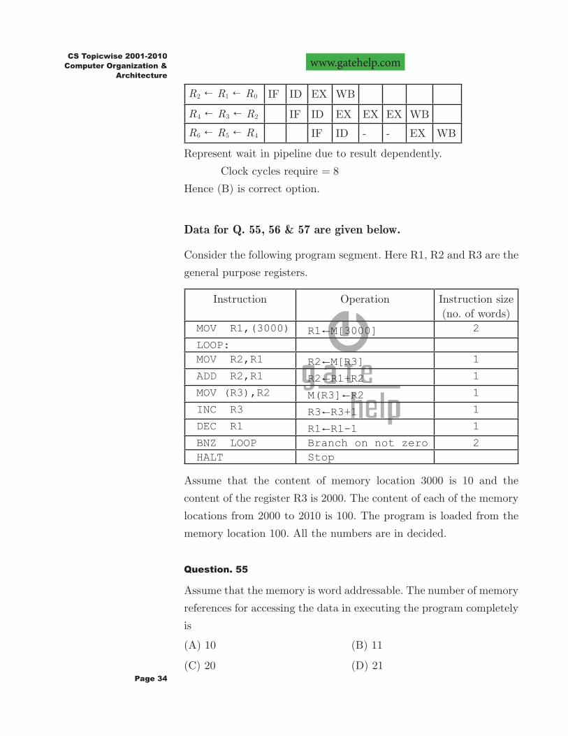
Instruction Words Location
MOV R1, (3000) 2 1000-1007
MOV R2, R1 1 1008-1011
ADD R2, R1 1 1012-1015
Page 36
www.gatehelp.comCS Topicwise 2001-2010
Computer Organization & Architecture
MOV (R3), R2 1 1016-1019
INC R3 1 1020-1023
DEC R1 1 1024-1027Interrupt occurs during execution of INC R3, So CPU will complete the execution of this instruction and then Push the next address 1024 to the stack, so after interrupt service the program can be resumed from next instruction.Hence (C) is correct option.
Data for Q. 58 & Q. 59 are given below.
Consider a machine with a byte addressable main memory of 216 bytes. Assume that a direct mapped data cache consisting of 32 lines of 64 bytes each is used in the system. A 50 50# two-dimensional array of bytes is stored in the main memory stating from memory location 1100H.Assume that the data cache is initially empty. The complete array is accessed twice. Assume that the contents of the data cache do not change in between the two accesses.
Question. 58
How many data cache misses will occur in total?
(A) 48 (B) 50
(C) 56 (D) 59
SOLUTION
Size of main memory 216 bytes. Size of Cache 32 64#= B 211= B Size of array 2500= BArray is stored in main memory but cache is empty. Size of Cache 2048= B So no. of page faults 2500 2048= − 452= For second access 452 2 904#= = Total 1356=Hence (C) is correct option.
Page 37
www.gatehelp.comCS Topicwise 2001-2010Computer Organization & Architecture
Question. 59
Which of the following lines of the data cache will be replaced by new blocks in accessing the array
(A) line 4 to line 11 (B) line 4 to line 12
(C) line 0 to line 7 (D) line 0 to line 8
SOLUTION
No of page faults 452= One line has 64 BSo the line at which these page faults will finish.
64452 7,=
So 0 to 7 lineHence (C) is correct option.
YEAR 2008
Question. 60
For a magnetic disk with concentric circular track, the latency is not linearly proportional to the seek distance due to
(A) non-uniform distribution of requests
(B) arm starting and stopping inertia
(C) higher capacity of tracks on the periphery of the platter
(D) use of unfair arm scheduling policies.
SOLUTION
Tracks on magnetic disks are concentric a seek is from me sector to other may or mayn’t be in different tracks.This seek distance is not proportional to latency since the tracks at periphery has higher diameter so high in capacity to store data.Hence (C) is correct option.
Question. 61
Which of the following is/are true of the auto increment addressing mode?
1. It is useful in creating self relocating code2. If it is included in an Instruction Set Architecture, then an
Page 38
www.gatehelp.comCS Topicwise 2001-2010
Computer Organization & Architecture
additional ALU is required for effective address calculation3. The amount of increment depends on the size of the data item
accessed.(A) 1 only (B) 2 only
(C) 3 only (D) 2 and 3 only
SOLUTION
In auto increment addressing mode the address where next data block to be stored is generated automatically depending upon the size of single data item required to store. So statement 3 is correct.Statement says that this mode is used for self relocating code, but this is false since self relocating code, takes always some address in memory.Statement 2 is also incorrect since no additional ALV is required.Hence (C) is correct option.
Question. 62
Which of the following must be true for the RFE (Return from Expectation) instruction on a general purpose processor.
1. It must be a trap instruction2. It must be a privileged instruction3. An exception can not be allowed to occur during execution of
an RFE instruction.(A) 1 only (B) 2 only
(C) 1 and 2 only (D) 1, 2 and 3 only
SOLUTION
RFE (Return From Exception) is a privileged trap trap instruction which is executed when exception occurs, so an exception is not allowed to execute.Hence (D) is correct option.
Question. 63
For inclusion to hold between two cache level L1 and L2 in a multilevel cache hierarchy, which of the following are necessary?
1. L1 must be a write-through cache2. L2 must be write-through cache
Page 39
www.gatehelp.comCS Topicwise 2001-2010Computer Organization & Architecture
3. The associativity of L2 must be greater that of L14. The L2 cache must be at least as large as the L1 cache(A) 4 only (B) 1 and 2 only
(C) 1, 2 and 4 only (D) 1, 2, 3 and 4
SOLUTION
Level 1 ( 1)L & Level 2 ( 2)L cache are placed between CPV & they can be both write through cache but this is not necessary.Associativity has no dependence but L2 cache must be at least as large as L1 cache, since all the words in L1 are also is L2.Hence (A) is correct option.
Question. 64
Which of the following are NOT true in a pipe lined processor?
1. Bypassing can handle alll Raw hazards.2. Register renaming can eliminate all register carried WAR
hazards.3. Control hazard penalties can be eliminated by dynamic branch
prediction.(A) 1 and 2 only (B) 1 and 3 only
(C) 2 and 3 only (D) 1,2 and 3
SOLUTION
In a pipelined processor by passing can’t handle all the row hazards. Registers carried WAR doesn’t have register naming as proper solution.And control hazard penalties are eliminated by delayed branching not by dynamic branch prediction.So all are false.Hence (D) is correct option.
Question. 65
The use of multiple register windows with overlap causes a reduction in the number of memory accesses for
1. Function locals and parameters
2. Register saves and restores
Page 40
www.gatehelp.comCS Topicwise 2001-2010
Computer Organization & Architecture
3. Instruction fetches
(A) 1 only (B) 2 only
(C) 3 only (D) 1,2 and 3
SOLUTION
Multiple register windows with overlap causes a reduction in the number of memory accesses for instruction fetching.Hence (C) is correct option.
Question. 66
In an instruction execution pipeline, the earliest that the data TLB (Translation Look aside Buffer) can be accessed is
(A) before effective address calculation has started
(B) during effective address calculation
(C) after effective address calculation has completed
(D) after data cache lookup has completed
SOLUTION
TLB is used during effective address calculation in an instruction execution pipeline.Hence (B) is correct option.
Data for Q. 67, 68 & 69 are given below.
Consider a machine a 2-way set associative data cache of size 64 kbytes and block size 16 bytes. The cache is managed using 32 bit virtual addressed and the page size is 4 kbytes. A program to be run on this machine begins as follows:
Double APR[1024]]1024]int i, j;/*Initalize array APR to 0.0*/for (i 0; i < 1024; i )= ++for )(j 0;k < 1024;j= ++APR[i] [j] 0.0;=
The size of double 8 bytes. Array APR is in memory stating at the beginning of virtual page FF0 000# and stored in row major order. The cache is initially empty and no pre-fetching is done. The only
Page 41
www.gatehelp.comCS Topicwise 2001-2010Computer Organization & Architecture
data memory references made by the program are those to array APR.
Question. 67
The total size of the tags in the cache directory is
(A) 32 kbits (B) 34 kbits
(C) 64 kbits (D) 68 kbits
SOLUTION
Virtual (CPU) address has 32= bits 2 way set associative cache size 64= KB Size of 1 set 32= KBRequire 15 bits for indexing. So Tag 32 15 17= − = Size of block 16= bytes 4= bits are required Index block word= + Block 15 4 11= − =
17 11 4
CPV address Size of tags = There are 217 bytes of tags in every set of cache. So total 17 2 1024# #= 34= KB.Hence (B) is correct option.
Question. 68
Which of the following array elements has the same cache index as APR [0][0]?
(A) APR[0][4] (B) APR[4][0]
(C) APR[0][5] (D) APR[5][0]
SOLUTION
Elements stored in row major order. Two elements should have same cache index (15 bits) & their tags may be different (17 bits).So [ ] [ ]APR % % the MSB 17 bits will be changed.
Page 42
www.gatehelp.comCS Topicwise 2001-2010
Computer Organization & Architecture
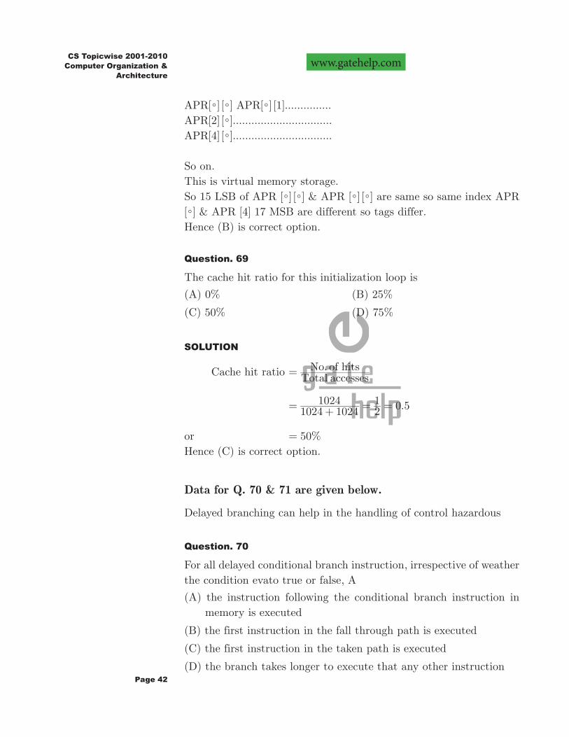
APR[ ] [ ]% % APR[ ] [ ]1% ...............APR[ ] [ ]2 % ................................APR[ ] [ ]4 % ................................
So on.This is virtual memory storage.So 15 LSB of APR [ ] [ ]% % & APR [ ] [ ]% % are same so same index APR [ ]% & APR [ ]4 17 MSB are different so tags differ.Hence (B) is correct option.
Question. 69
The cache hit ratio for this initialization loop is
(A) 0% (B) 25%
(C) 50% (D) 75%
SOLUTION
Cache hit ratio Total accessesNo. of hits=
.1024 10241024
21 0 5= + = =
or %50=Hence (C) is correct option.
Data for Q. 70 & 71 are given below.
Delayed branching can help in the handling of control hazardous
Question. 70
For all delayed conditional branch instruction, irrespective of weather the condition evato true or false, A
(A) the instruction following the conditional branch instruction in memory is executed
(B) the first instruction in the fall through path is executed
(C) the first instruction in the taken path is executed
(D) the branch takes longer to execute that any other instruction
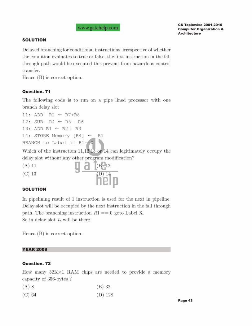
Page 43
www.gatehelp.comCS Topicwise 2001-2010Computer Organization & Architecture
SOLUTION
Delayed branching for conditional instructions, irrespective of whether the condition evaluates to true or false, the first instruction in the fall through path would be executed this prevent from hazardous control transfer.Hence (B) is correct option.
Question. 71
The following code is to run on a pipe lined processor with one branch delay slot
11: ADD R2 ! R7+R812: SUB R4 ! R5− R613: ADD R1 ! R2+ R314: STORE Memory [R4] ! R1BRANCH to Label if R1==0
Which of the instruction 11,12,13 or 14 can legitimately occupy the delay slot without any other program modification?
(A) 11 (B) 12
(C) 13 (D) 14
SOLUTION
In pipelining result of 1 instruction is used for the next in pipeline. Delay slot will be occupied by the next instruction in the fall through path. The branching instruction 0R1 == goto Label X.So in delay slot I2 will be there.
Hence (B) is correct option.
YEAR 2009
Question. 72
How many 32K#1 RAM chips are needed to provide a memory capacity of 356-bytes ?
(A) 8 (B) 32
(C) 64 (D) 128
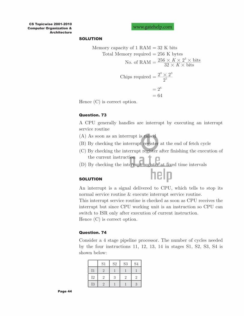
Page 44
www.gatehelp.comCS Topicwise 2001-2010
Computer Organization & Architecture
SOLUTION
Memory capacity of 1 RAM 32= K bits Total Memory required 256= K bytes
No. of RAM 32256 2
KK
bitsbits3
# ## # #=
Chips required 2
2 25
8 3#=
26= 64=Hence (C) is correct option.
Question. 73
A CPU generally handles are interrupt by executing an interrupt service routine
(A) As soon as an interrupt is raised
(B) By checking the interrupt register at the end of fetch cycle
(C) By checking the interrupt register after finishing the execution of the current instruction
(D) By checking the interrupt register at fixed time intervals
SOLUTION
An interrupt is a signal delivered to CPU, which tells to stop its normal service routine & execute interrupt service routine.This interrupt service routine is checked as soon as CPU receives the interrupt but since CPU working unit is an instruction so CPU can switch to ISR only after execution of current instruction.Hence (C) is correct option.
Question. 74
Consider a 4 stage pipeline processor. The number of cycles needed by the four instructions 11, 12, 13, 14 in stages S1, S2, S3, S4 is shown below:
S1 S2 S3 S4
I1 2 1 1 1
I2 2 3 2 2
I3 2 1 1 3
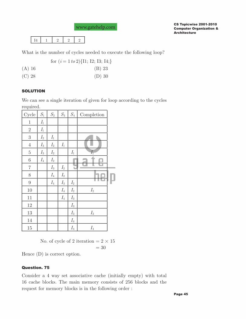
Page 45
www.gatehelp.comCS Topicwise 2001-2010Computer Organization & Architecture
I4 1 2 2 2
What is the number of cycles needed to execute the following loop?
for ( )i to1 2= {I1; I2; I3; I4;}
(A) 16 (B) 23
(C) 28 (D) 30
SOLUTION
We can see a single iteration of given for loop according to the cycles required.
Cycle S1 S2 S3 S4 Completion
1 I1
2 I1
3 I2 I1
4 I3 I2 I1
5 I3 I2 I1 I1
6 I4 I2
7 I3 I2
8 I4 I2
9 I4 I3 I2
10 I4 I2 I2
11 I4 I3
12 I3
13 I3 I3
14 I4
15 I4 I4
No. of cycle of 2 iteration 2 15#= 30=Hence (D) is correct option.
Question. 75
Consider a 4 way set associative cache (initially empty) with total 16 cache blocks. The main memory consists of 256 blocks and the request for memory blocks is in the following order :
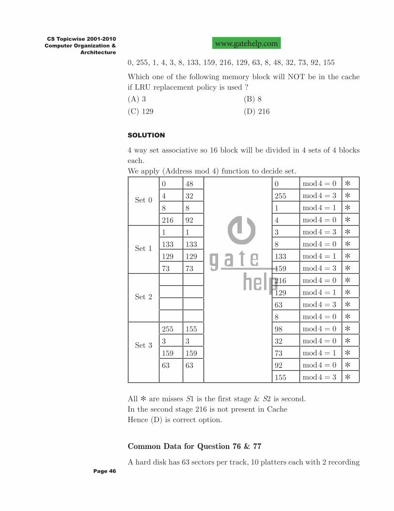
Page 46
www.gatehelp.comCS Topicwise 2001-2010
Computer Organization & Architecture
0, 255, 1, 4, 3, 8, 133, 159, 216, 129, 63, 8, 48, 32, 73, 92, 155
Which one of the following memory block will NOT be in the cache if LRU replacement policy is used ?
(A) 3 (B) 8
(C) 129 (D) 216
SOLUTION
4 way set associative so 16 block will be divided in 4 sets of 4 blocks each.We apply (Address mod 4) function to decide set.
Set 0
0 48 0 mod4 0= )
4 32 255 mod4 3= )
8 8 1 mod4 1= )
216 92 4 mod4 0= )
Set 1
1 1 3 mod4 3= )
133 133 8 mod4 0= )
129 129 133 mod4 1= )
73 73 159 mod4 3= )
Set 2
216 mod4 0= )
129 mod4 1= )
63 mod4 3= )
8 mod4 0= )
Set 3
255 155 98 mod4 0= )
3 3 32 mod4 0= )
159 159 73 mod4 1= )
63 63 92 mod4 0= )
155 mod4 3= )
All ) are misses S1 is the first stage & S2 is second.In the second stage 216 is not present in CacheHence (D) is correct option.
Common Data for Question 76 & 77
A hard disk has 63 sectors per track, 10 platters each with 2 recording
Page 47
www.gatehelp.comCS Topicwise 2001-2010Computer Organization & Architecture
surfaces and 1000 cylinders. The address of a sector is given as a triple
, ,c h s , where c is the cylinder number, h is the surface number and
s is the sector number. Thus, the 0th sector is addressed as , ,0 0 0 ,
the 1st sector as , ,0 0 1 , and so on.
Question. 76
The address , ,400 16 29 , corresponds to sector number:
(A) 505035 (B) 505036
(C) 505037 (D) 505038
SOLUTION
Each cylinder has 10 platters or 20 recording surfaces
or 63 20# sector 1260= sectors.
Each recording surface has 63 sectors.
So , ,400 16 297< , ,c h s< >= 400 1260 16 63 29# #+ + 505037
Hence (C) is correct option.
Question. 77
The address of 1039th sector is
(A) , ,0 15 31 (B) , ,0 16 30
(C) , ,0 16 31 (D) , ,0 17 31
SOLUTION
1 cylinder has 1260 sectors
So address for 1039th sector.
C 0=Each surface has 63 sectors.
Total surface here 631039 16= = surfaces
Remainder here 31 sectors
So , ,0 16 31< >.
Hence (C) is correct option.
Page 48
www.gatehelp.comCS Topicwise 2001-2010
Computer Organization & Architecture
YEAR 2010
Question. 78
A main memory unit with a capacity of 4 megabytes is build using 1 1M bit DRAM# − chips. Each DRAM chip has 1K rows of cells with 1 K cells in each row. The time taken for a single refresh operation is 100 nanoseconds. The time required to perform one refresh operation on all the cells in the memory unit is
(A) 100 nanoseconds (B) 100 210) nanoseconds
(C) 100 220) nanoseconds (D) 3200 220) nanoseconds
SOLUTION
Size of main memory 4= MB 1 DRAM size 1= Mb
No. of chips required M bM b
14 8
# ## # #=
32=1 DRAM has 1 K rows1 ROW has 1 K cells Total cells in 1 DRAM K 22 20= = In 32 DRAM 32 220
#= Cells1 cell refresh take 100 ns.So total refresh time 32 100 220
# #= ns 3200 220
#= ns.
Hence (D) is correct option.
Question. 79
A-5 stage pipelined processor has Instruction Fetch. (IF), Instruction Decode (ID), Operand Fetch (OF), Perform Operation (PO) and Write Operand (WO) stages. The IF, ID, OF and WO stages take 1 clock cycle each for any instruction. The PO stage takes 1 clock cycle for ADD and SUB instruction. The PO stage takes 1 stake clock cycle for ADD and SUB instructions 3 clock cycles for MUL instruction, and 6 clock cycles for DIV instruction respectively. Operand forwarding is used in the pipeline. What is the number of clock cycles needed to execute the following sequence of instructions ?
Page 49
www.gatehelp.comCS Topicwise 2001-2010Computer Organization & Architecture
Instruction Meaning of instruction
I0: MUL , ,R R R2 0 1 R R R2 0 1! )
I1: DIV , ,R R R5 3 4 /R R R5 3 4!
I2: ADD , ,R R R2 5 2 R R R2 5 2! +
I3: SUB , ,R R R5 2 6 R R R5 2 6! −
(A) 13 (B) 15
(C) 17 (D) 19
SOLUTION
The order of operations IF ID OF PO WO" " " "
Figure
Here A ( / ) ,R R R R3 4 2 6= +
So we can see that all the instruction can be executed in 17 clock cycles using piplining.
Hence (C) is correct option.
Question. 80
The program below uses six temporary variables , , , , ,a b c d e f
a 1=b 10=c 20=d a b= +e c d= +f c e= +b c e= +e b f= +d e5= +
Assuming that all operations take their operands from register, what is the minimum number of registers needed to execute this program without spilling ?
(A) 2 (B) 3
(C) 4 (D) 6
Page 50
www.gatehelp.comCS Topicwise 2001-2010
Computer Organization & Architecture
SOLUTION
Replacement
R1 R2 R3
a b c
d b c
d e c
f e c
f b c
f e c
f e dSo all the operations done using 3 registers only.Hence (B) is correct option.
Common Data for Questions 81 & 82
A computer system has an L1 and L2 cache, an L2 cache, and a main memory unit connected as shown below. The block size in L1 cache is 4 words. The block size is L2 cache is 16 words. The memory access times are 2 nanoseconds, 20 nanoseconds and 200 nanoseconds for L1 cache, L2 cache and main memory unity respectively.
Question. 81
When there is a miss in L1 cache and a hit in L2 cache, a block is transferred form L2 cache to L1 cache. What is the time taken for this transfer ?
(A) 2 nanoseconds (B) 20 nanoseconds
(C) 22 nanoseconds (D) 88 nanoseconds
SOLUTION
Each block is L2 Cache is 4 times L1 Cache. So far 1 block miss in L1 Cache the block from L2 to L1 will be transferred, but L2 block has size 16 words & L1 data bus of 4 words, so 2L4 & L4 1 access are
Page 51
www.gatehelp.comCS Topicwise 2001-2010Computer Organization & Architecture
required. 4 2 4 20# #+ 8 80+ 88 nsHence (D) is correct option.
Question. 82
When there is a miss in both L1 cache and L2 cache, first a block is transferred from memory to L2 cache, and then a block is transferred from L2 cache to L1 cache. What is the total time taken for these transfers ?
(A) 222 nanoseconds (B) 888 nanoseconds
(C) 902 nanoseconds (D) 968 nanoseconds
SOLUTION
Miss in both L1 & L2. Cause main memory to transfer that block in both cache.1 block of Main memory has 16 words but data bus of L2 has only 4 words. So 4 access of Main memory & 4 access of L2 Cache required to update L2 4 20 4 200# #+ 80 800+ 880= ns
Now L2 updates L1, this takes 4 access to L1 & 4 access to L2 4 2 4 20# #+ 8 80+ 88= ns Total time 880 88= + 968= nsHence (D) is correct option.
**********

By NODIA and Company
Available in Two Volumes


![[Public Administration Mains] Complete Topicwise Analysis 2001-09](https://img.pdfslide.us/doc/110x75/577cd56b1a28ab9e789abb82/public-administration-mains-complete-topicwise-analysis-2001-09.jpg)