Embed Size (px)
Citation preview
Computer Organization and Architecture
Memory SystemsCache Memory
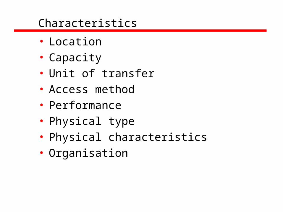
Characteristics
• Location• Capacity• Unit of transfer• Access method• Performance• Physical type• Physical characteristics• Organisation
Location
• CPU• Internal• External
Capacity
• Word size—The natural unit of organisation
• Number of words—or Bytes
Unit of Transfer
• Internal—Usually governed by data bus width
• External—Usually a block which is much larger than
a word
• Addressable unit—Smallest location which can be uniquely
addressed—Word internally—Cluster on M$ disks
Access Methods (1)
• Sequential—Start at the beginning and read through
in order—Access time depends on location of data
and previous location—e.g. tape
• Direct—Individual blocks have unique address—Access is by jumping to vicinity plus
sequential search—Access time depends on location and
previous location—e.g. disk
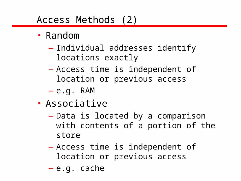
Access Methods (2)
• Random—Individual addresses identify locations
exactly—Access time is independent of location or
previous access—e.g. RAM
• Associative—Data is located by a comparison with
contents of a portion of the store—Access time is independent of location or
previous access—e.g. cache
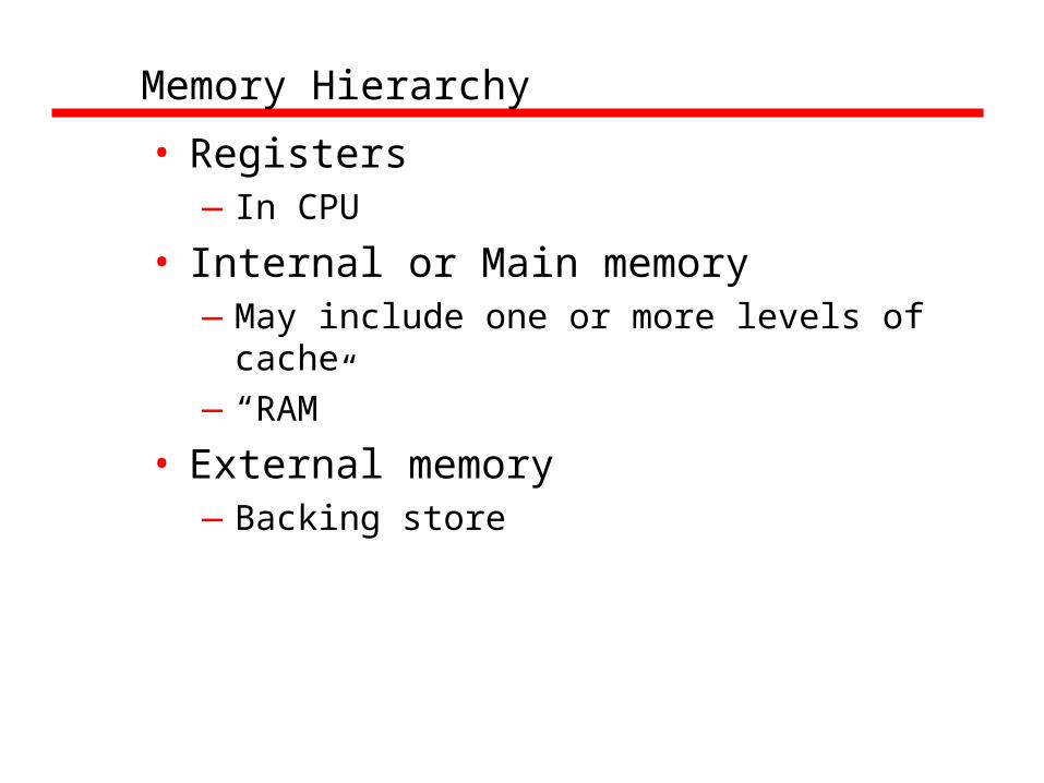
Memory Hierarchy
• Registers—In CPU
• Internal or Main memory—May include one or more levels of cache—“RAM”
• External memory—Backing store
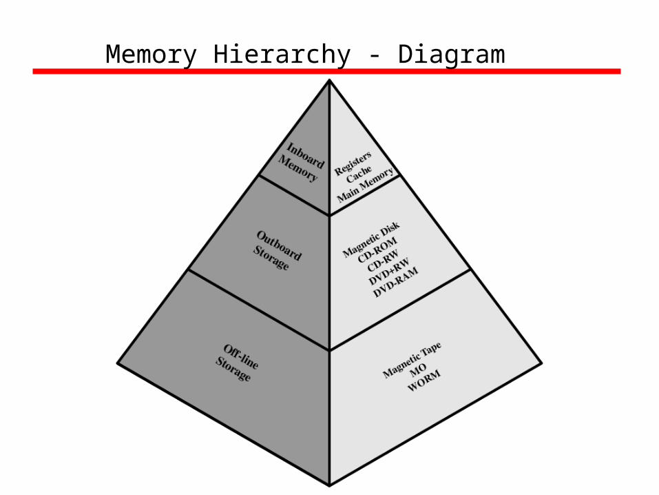
Memory Hierarchy - Diagram
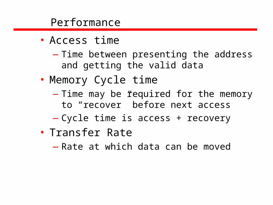
Performance
• Access time—Time between presenting the address
and getting the valid data
• Memory Cycle time—Time may be required for the memory to
“recover” before next access—Cycle time is access + recovery
• Transfer Rate—Rate at which data can be moved
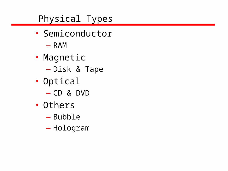
Physical Types
• Semiconductor—RAM
• Magnetic—Disk & Tape
• Optical—CD & DVD
• Others—Bubble—Hologram
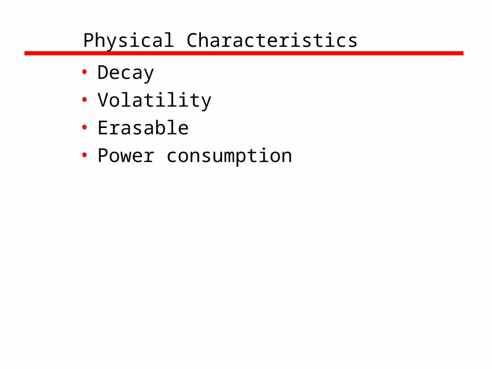
Physical Characteristics
• Decay• Volatility• Erasable• Power consumption
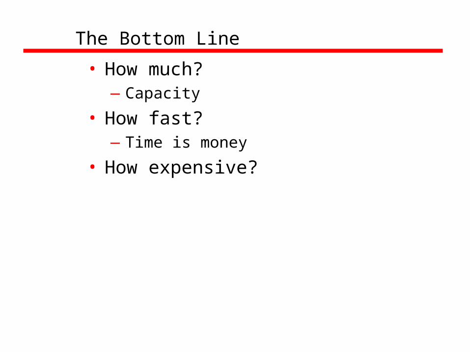
The Bottom Line
• How much?—Capacity
• How fast?—Time is money
• How expensive?
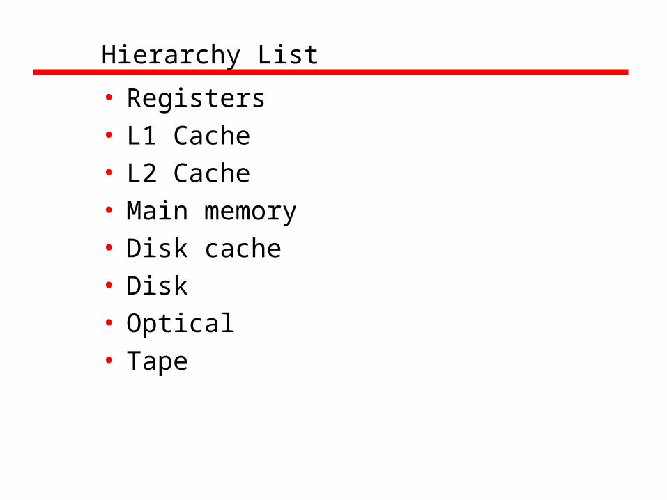
Hierarchy List
• Registers• L1 Cache• L2 Cache• Main memory• Disk cache• Disk• Optical• Tape
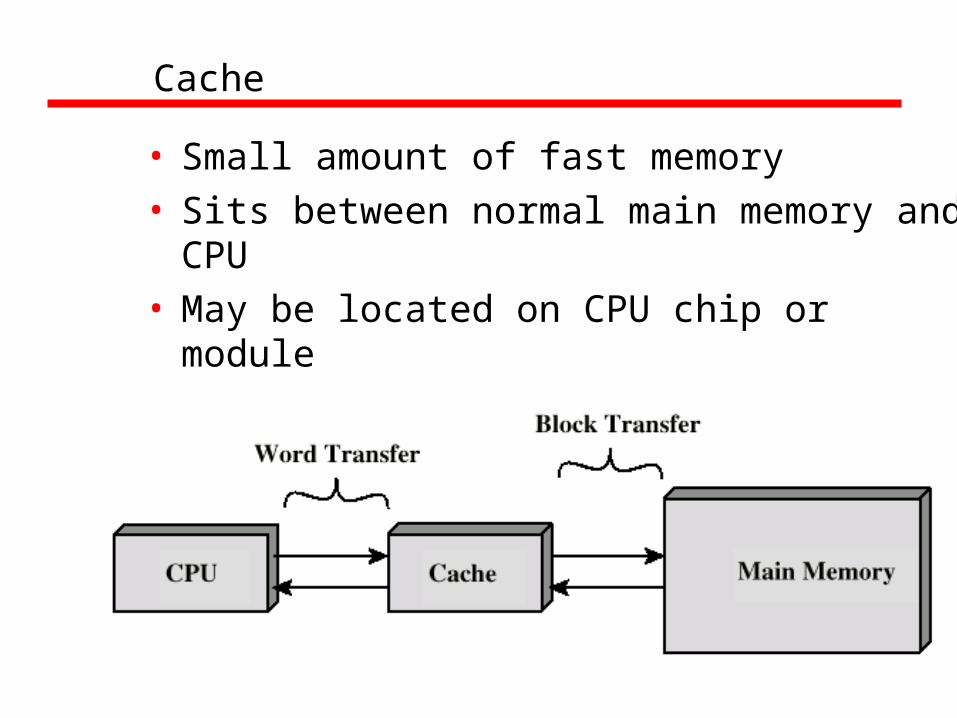
Cache
• Small amount of fast memory• Sits between normal main memory and
CPU• May be located on CPU chip or module
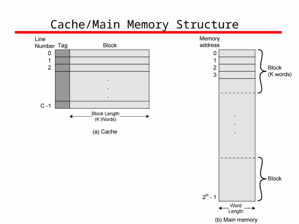
Cache/Main Memory Structure
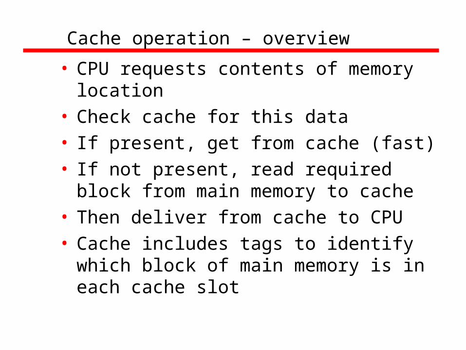
Cache operation – overview
• CPU requests contents of memory location
• Check cache for this data• If present, get from cache (fast)• If not present, read required block
from main memory to cache• Then deliver from cache to CPU• Cache includes tags to identify which
block of main memory is in each cache slot
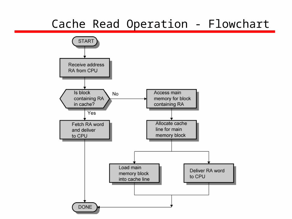
Cache Read Operation - Flowchart
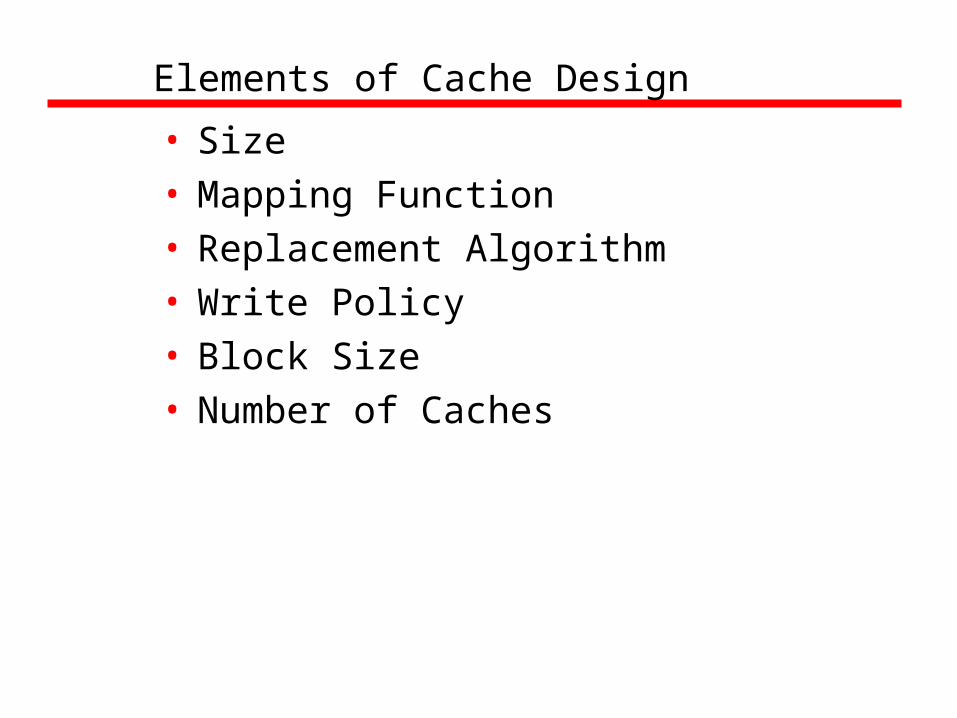
Elements of Cache Design
• Size• Mapping Function• Replacement Algorithm• Write Policy• Block Size• Number of Caches
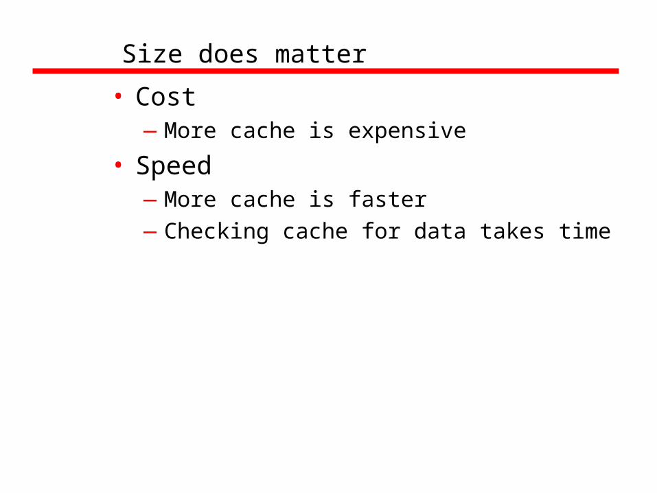
Size does matter
• Cost—More cache is expensive
• Speed—More cache is faster—Checking cache for data takes time
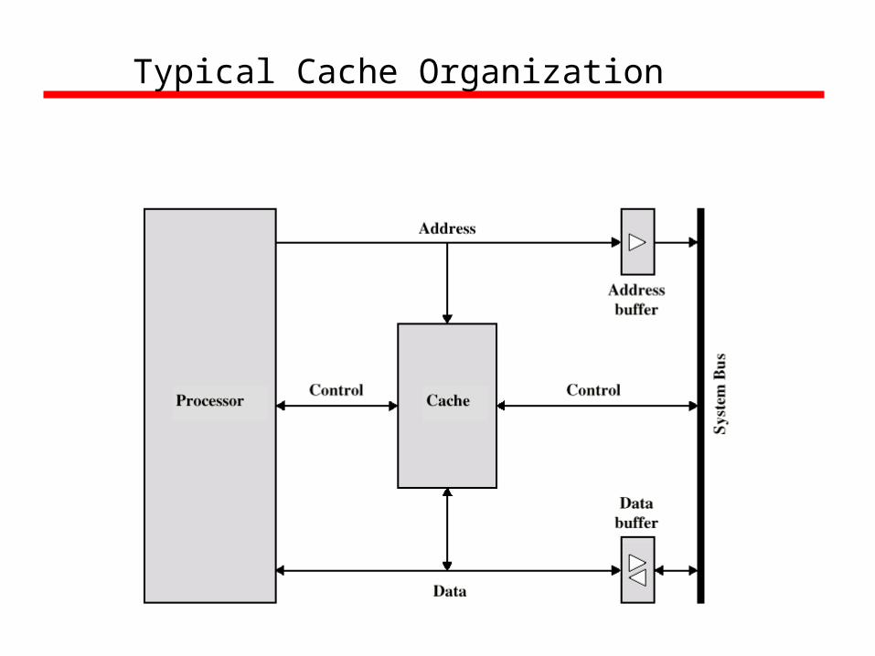
Typical Cache Organization
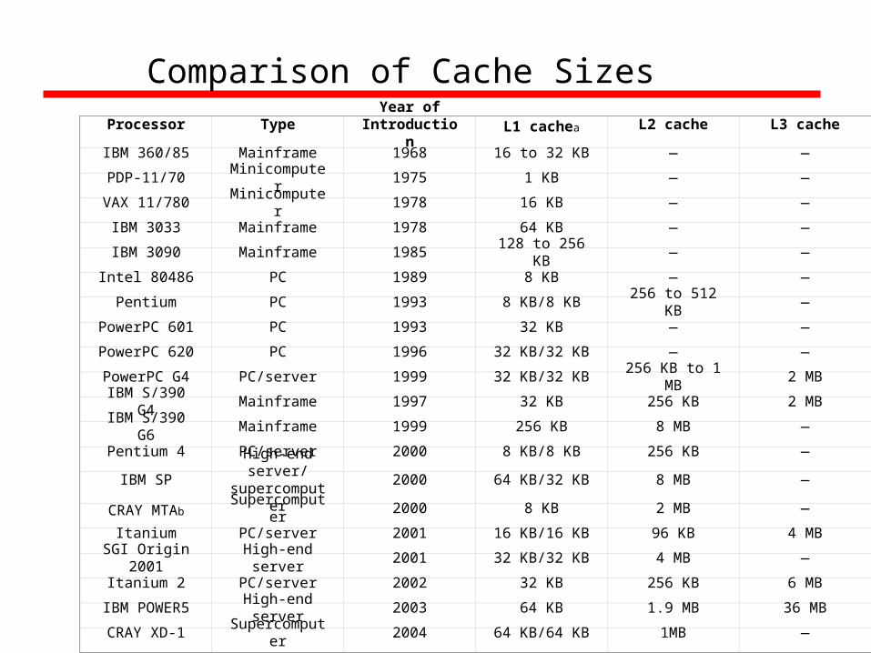
Comparison of Cache SizesProcessor Type
Year of Introduction L1 cachea L2 cache L3 cache
IBM 360/85 Mainframe 1968 16 to 32 KB — —
PDP-11/70 Minicomputer 1975 1 KB — —
VAX 11/780 Minicomputer 1978 16 KB — —
IBM 3033 Mainframe 1978 64 KB — —
IBM 3090 Mainframe 1985 128 to 256 KB — —
Intel 80486 PC 1989 8 KB — —
Pentium PC 1993 8 KB/8 KB 256 to 512 KB —
PowerPC 601 PC 1993 32 KB — —
PowerPC 620 PC 1996 32 KB/32 KB — —
PowerPC G4 PC/server 1999 32 KB/32 KB 256 KB to 1 MB 2 MB
IBM S/390 G4 Mainframe 1997 32 KB 256 KB 2 MB
IBM S/390 G6 Mainframe 1999 256 KB 8 MB —
Pentium 4 PC/server 2000 8 KB/8 KB 256 KB —
IBM SPHigh-end server/ supercomputer
2000 64 KB/32 KB 8 MB —
CRAY MTAb Supercomputer 2000 8 KB 2 MB —
Itanium PC/server 2001 16 KB/16 KB 96 KB 4 MB
SGI Origin 2001 High-end server 2001 32 KB/32 KB 4 MB —
Itanium 2 PC/server 2002 32 KB 256 KB 6 MB
IBM POWER5 High-end server 2003 64 KB 1.9 MB 36 MB
CRAY XD-1 Supercomputer 2004 64 KB/64 KB 1MB —
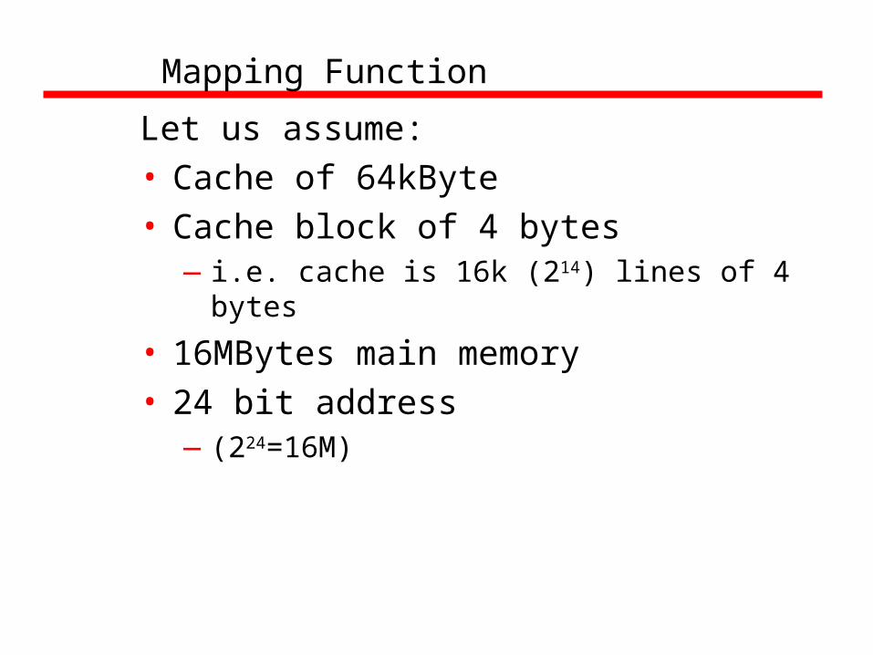
Mapping Function
Let us assume:• Cache of 64kByte• Cache block of 4 bytes
—i.e. cache is 16k (214) lines of 4 bytes
• 16MBytes main memory• 24 bit address
—(224=16M)
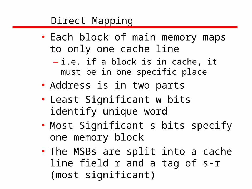
Direct Mapping
• Each block of main memory maps to only one cache line—i.e. if a block is in cache, it must be in
one specific place
• Address is in two parts• Least Significant w bits identify
unique word• Most Significant s bits specify one
memory block• The MSBs are split into a cache line
field r and a tag of s-r (most significant)
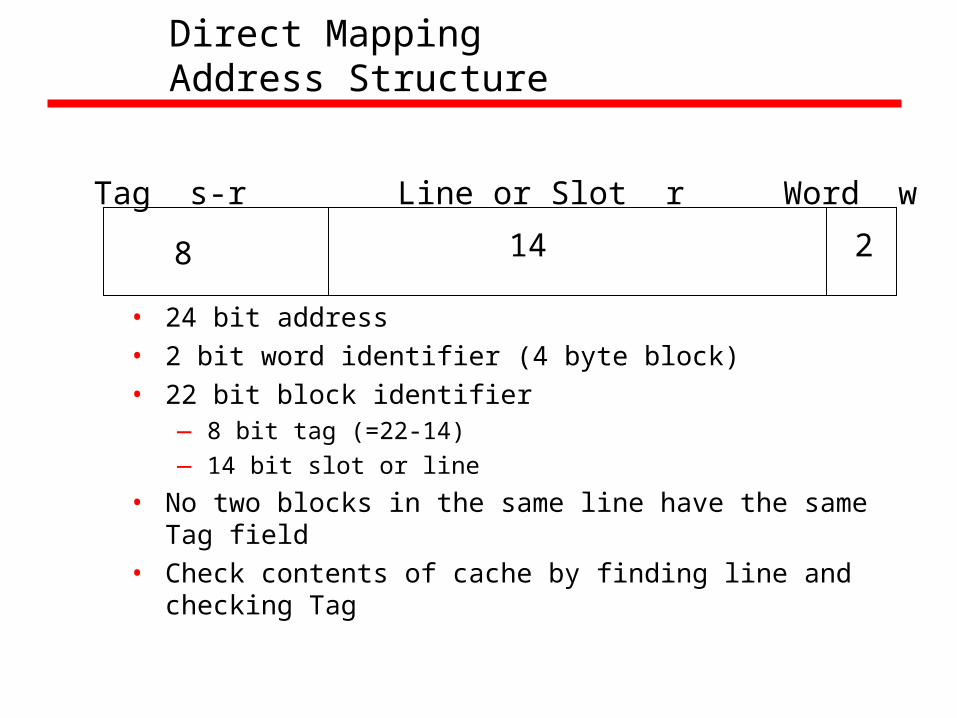
Direct MappingAddress Structure
Tag s-r Line or Slot r Word w
8 14 2
• 24 bit address• 2 bit word identifier (4 byte block)• 22 bit block identifier
— 8 bit tag (=22-14)— 14 bit slot or line
• No two blocks in the same line have the same Tag field
• Check contents of cache by finding line and checking Tag
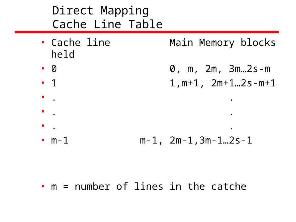
Direct Mapping Cache Line Table
• Cache line Main Memory blocks held• 0 0, m, 2m, 3m…2s-m• 1 1,m+1, 2m+1…2s-
m+1• . .• . .• . .• m-1 m-1, 2m-1,3m-1…2s-1
• m = number of lines in the catche
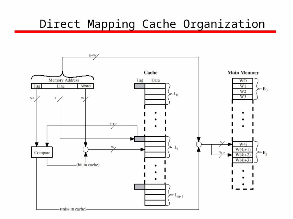
Direct Mapping Cache Organization
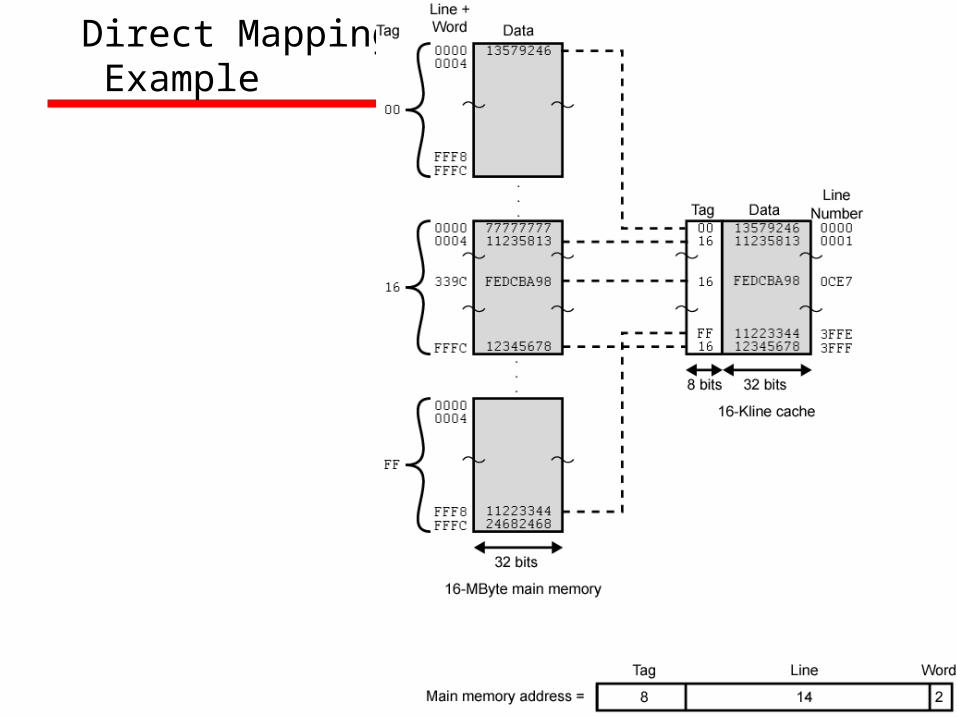
Direct Mapping Example
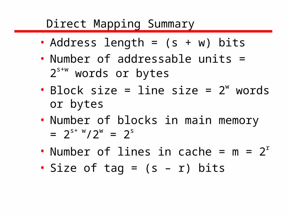
Direct Mapping Summary
• Address length = (s + w) bits• Number of addressable units = 2s+w
words or bytes• Block size = line size = 2w words or
bytes• Number of blocks in main memory =
2s+ w/2w = 2s
• Number of lines in cache = m = 2r
• Size of tag = (s – r) bits
Direct Mapping pros & cons
• Simple• Inexpensive• Fixed location for given block
—If a program accesses 2 blocks that map to the same line repeatedly, cache misses are very high
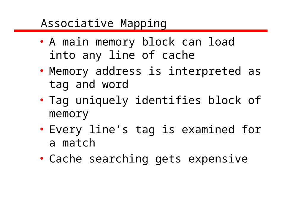
Associative Mapping
• A main memory block can load into any line of cache
• Memory address is interpreted as tag and word
• Tag uniquely identifies block of memory
• Every line’s tag is examined for a match
• Cache searching gets expensive
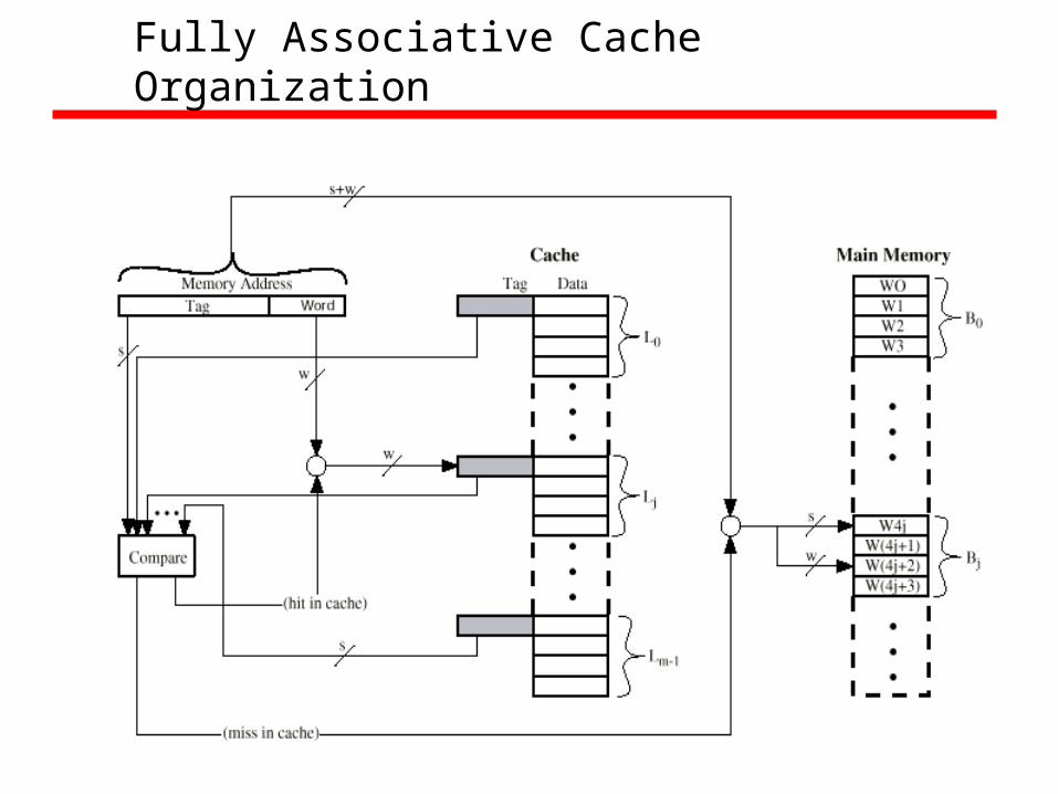
Fully Associative Cache Organization
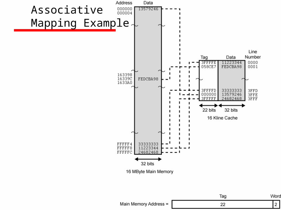
Associative Mapping Example
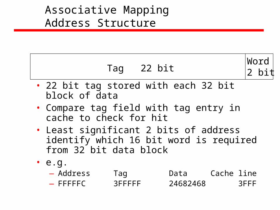
Tag 22 bitWord2 bit
Associative MappingAddress Structure
• 22 bit tag stored with each 32 bit block of data
• Compare tag field with tag entry in cache to check for hit
• Least significant 2 bits of address identify which 16 bit word is required from 32 bit data block
• e.g.—Address Tag Data Cache
line—FFFFFC 3FFFFF 24682468 3FFF
Associative Mapping Summary
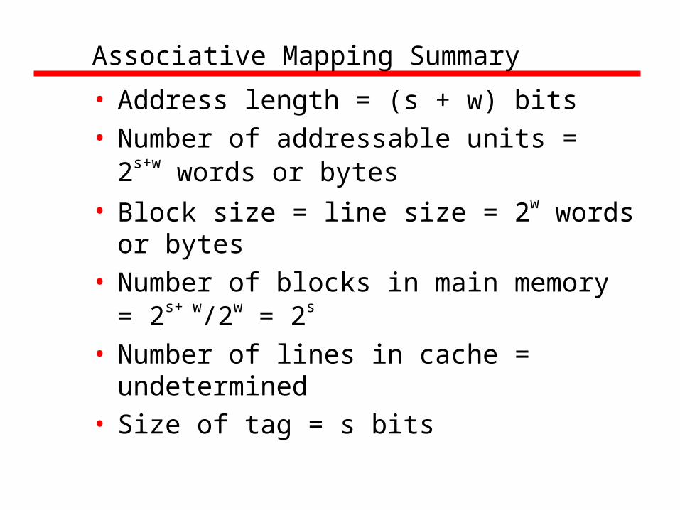
• Address length = (s + w) bits• Number of addressable units = 2s+w
words or bytes• Block size = line size = 2w words or
bytes• Number of blocks in main memory =
2s+ w/2w = 2s
• Number of lines in cache = undetermined
• Size of tag = s bits
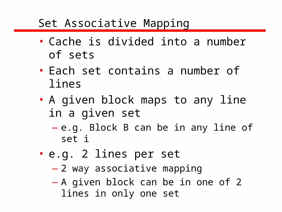
Set Associative Mapping
• Cache is divided into a number of sets• Each set contains a number of lines• A given block maps to any line in a
given set—e.g. Block B can be in any line of set i
• e.g. 2 lines per set—2 way associative mapping—A given block can be in one of 2 lines in
only one set
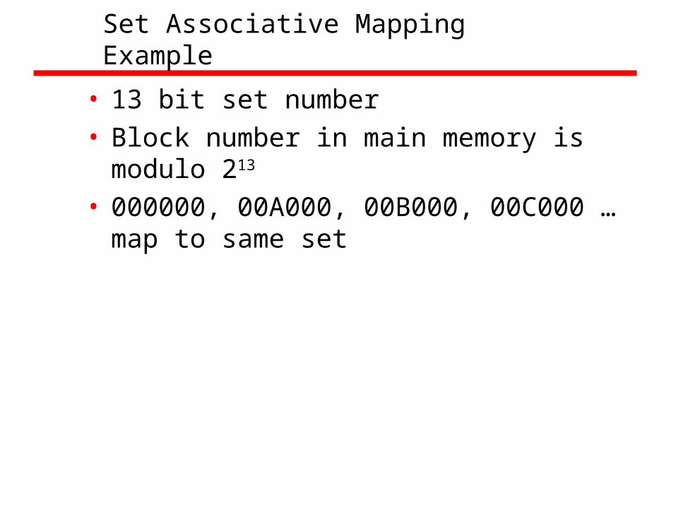
Set Associative MappingExample
• 13 bit set number• Block number in main memory is
modulo 213 • 000000, 00A000, 00B000, 00C000 …
map to same set
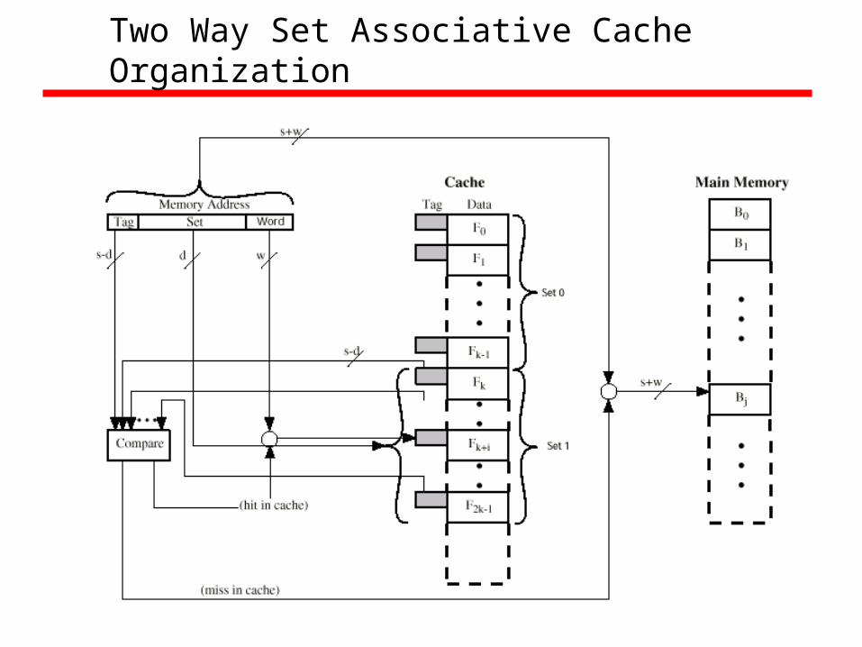
Two Way Set Associative Cache Organization
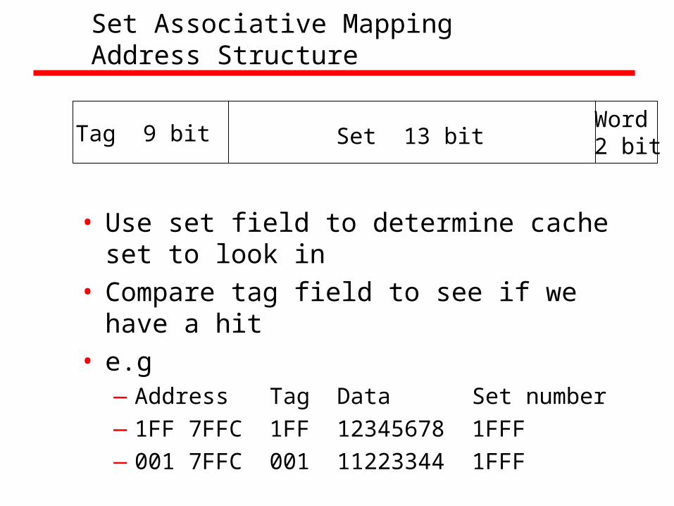
Set Associative MappingAddress Structure
• Use set field to determine cache set to look in
• Compare tag field to see if we have a hit
• e.g—Address Tag Data Set number—1FF 7FFC 1FF 12345678 1FFF—001 7FFC 001 11223344 1FFF
Tag 9 bit Set 13 bitWord2 bit
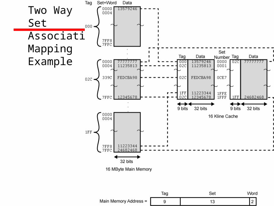
Two Way Set Associative Mapping Example
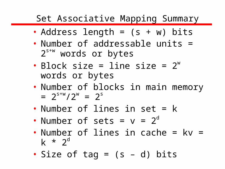
Set Associative Mapping Summary
• Address length = (s + w) bits• Number of addressable units = 2s+w
words or bytes• Block size = line size = 2w words or
bytes• Number of blocks in main memory =
2s+w/2w = 2s
• Number of lines in set = k• Number of sets = v = 2d
• Number of lines in cache = kv = k * 2d
• Size of tag = (s – d) bits
Replacement Algorithms (1)Direct mapping
• No choice• Each block only maps to one line• Replace that line
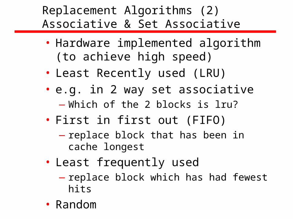
Replacement Algorithms (2)Associative & Set Associative
• Hardware implemented algorithm (to achieve high speed)
• Least Recently used (LRU)• e.g. in 2 way set associative
—Which of the 2 blocks is lru?
• First in first out (FIFO)—replace block that has been in cache
longest
• Least frequently used—replace block which has had fewest hits
• Random
Write Policy
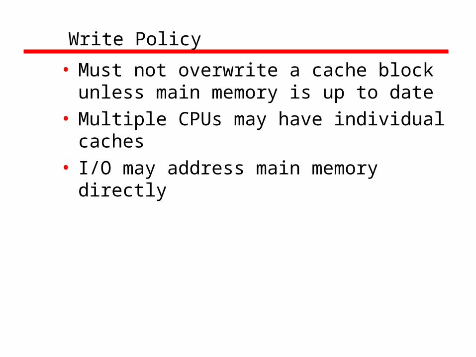
• Must not overwrite a cache block unless main memory is up to date
• Multiple CPUs may have individual caches
• I/O may address main memory directly
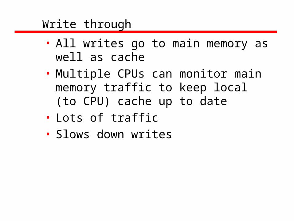
Write through
• All writes go to main memory as well as cache
• Multiple CPUs can monitor main memory traffic to keep local (to CPU) cache up to date
• Lots of traffic• Slows down writes
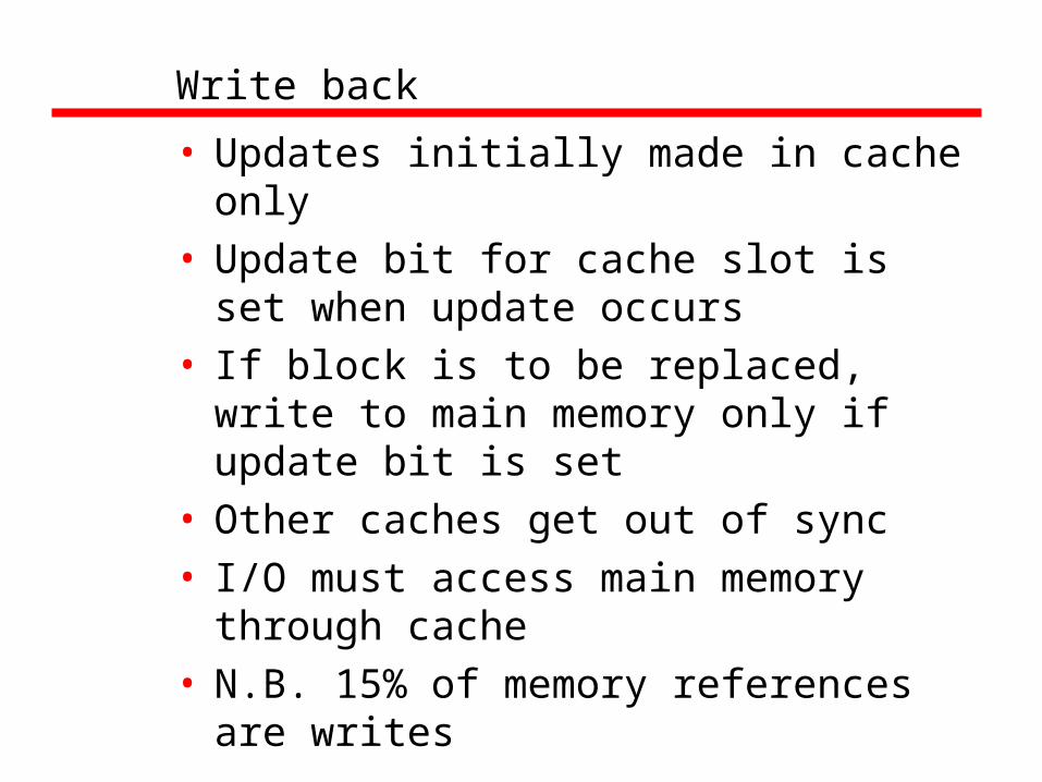
Write back
• Updates initially made in cache only• Update bit for cache slot is set when
update occurs• If block is to be replaced, write to
main memory only if update bit is set
• Other caches get out of sync• I/O must access main memory
through cache• N.B. 15% of memory references are
writes
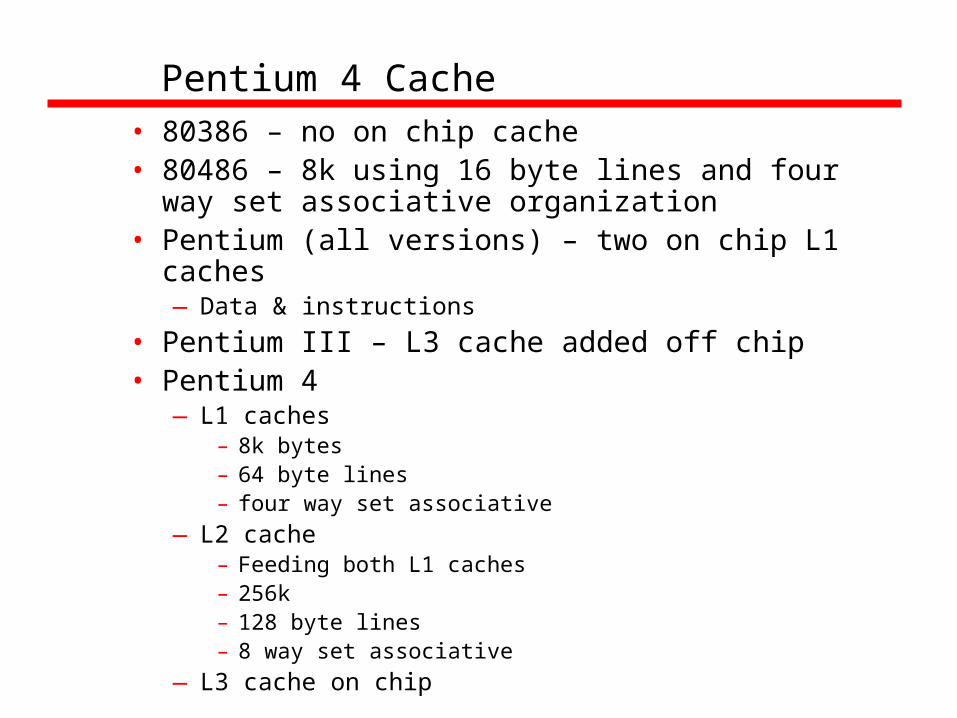
Pentium 4 Cache• 80386 – no on chip cache• 80486 – 8k using 16 byte lines and four way
set associative organization• Pentium (all versions) – two on chip L1 caches
—Data & instructions
• Pentium III – L3 cache added off chip• Pentium 4
—L1 caches– 8k bytes– 64 byte lines– four way set associative
—L2 cache – Feeding both L1 caches– 256k– 128 byte lines– 8 way set associative
—L3 cache on chip
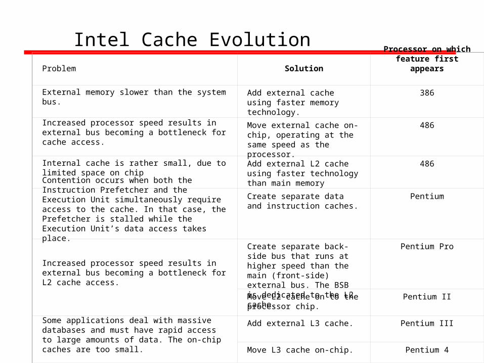
Intel Cache EvolutionProblem Solution
Processor on which feature first appears
External memory slower than the system bus. Add external cache using faster memory technology.
386
Increased processor speed results in external bus becoming a bottleneck for cache access.
Move external cache on-chip, operating at the same speed as the processor.
486
Internal cache is rather small, due to limited space on chip
Add external L2 cache using faster technology than main memory
486
Contention occurs when both the Instruction Prefetcher and the Execution Unit simultaneously require access to the cache. In that case, the Prefetcher is stalled while the Execution Unit’s data access takes place.
Create separate data and instruction caches.
Pentium
Increased processor speed results in external bus becoming a bottleneck for L2 cache access.
Create separate back-side bus that runs at higher speed than the main (front-side) external bus. The BSB is dedicated to the L2 cache.
Pentium Pro
Move L2 cache on to the processor chip.
Pentium II
Some applications deal with massive databases and must have rapid access to large amounts of data. The on-chip caches are too small.
Add external L3 cache. Pentium III
Move L3 cache on-chip. Pentium 4
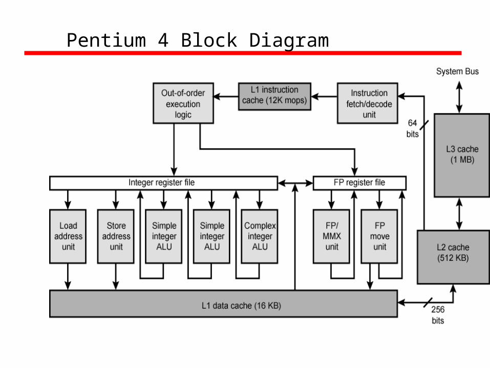
Pentium 4 Block Diagram
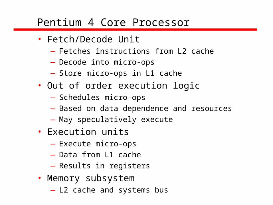
Pentium 4 Core Processor
• Fetch/Decode Unit—Fetches instructions from L2 cache—Decode into micro-ops—Store micro-ops in L1 cache
• Out of order execution logic—Schedules micro-ops—Based on data dependence and resources—May speculatively execute
• Execution units—Execute micro-ops—Data from L1 cache—Results in registers
• Memory subsystem—L2 cache and systems bus
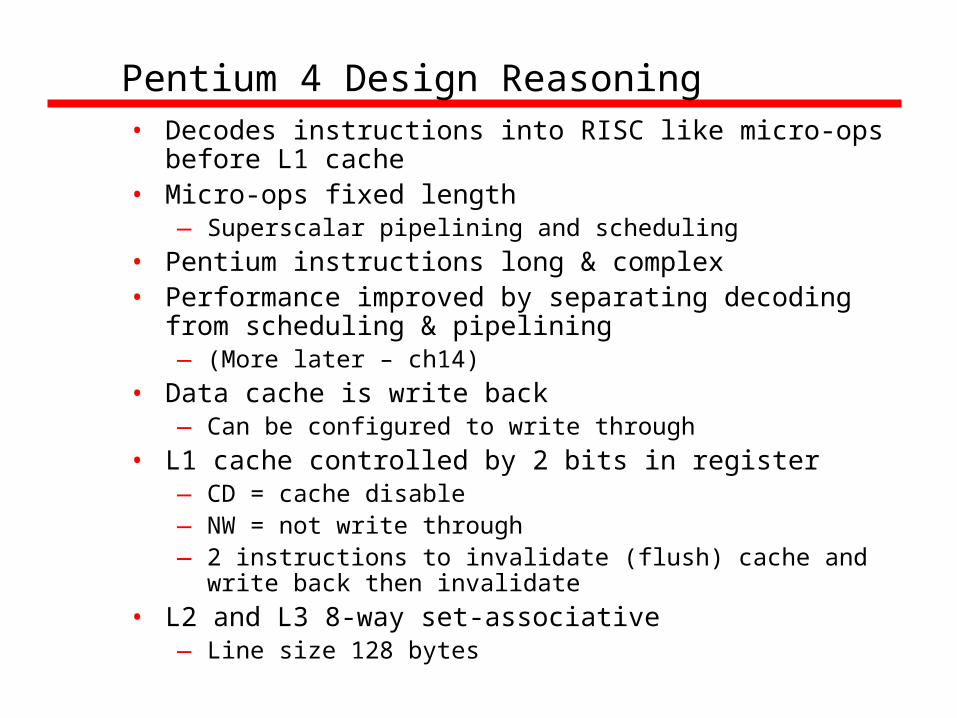
Pentium 4 Design Reasoning• Decodes instructions into RISC like micro-ops before
L1 cache• Micro-ops fixed length
— Superscalar pipelining and scheduling• Pentium instructions long & complex• Performance improved by separating decoding from
scheduling & pipelining— (More later – ch14)
• Data cache is write back— Can be configured to write through
• L1 cache controlled by 2 bits in register— CD = cache disable— NW = not write through— 2 instructions to invalidate (flush) cache and write back
then invalidate• L2 and L3 8-way set-associative
— Line size 128 bytes
PowerPC Cache Organization
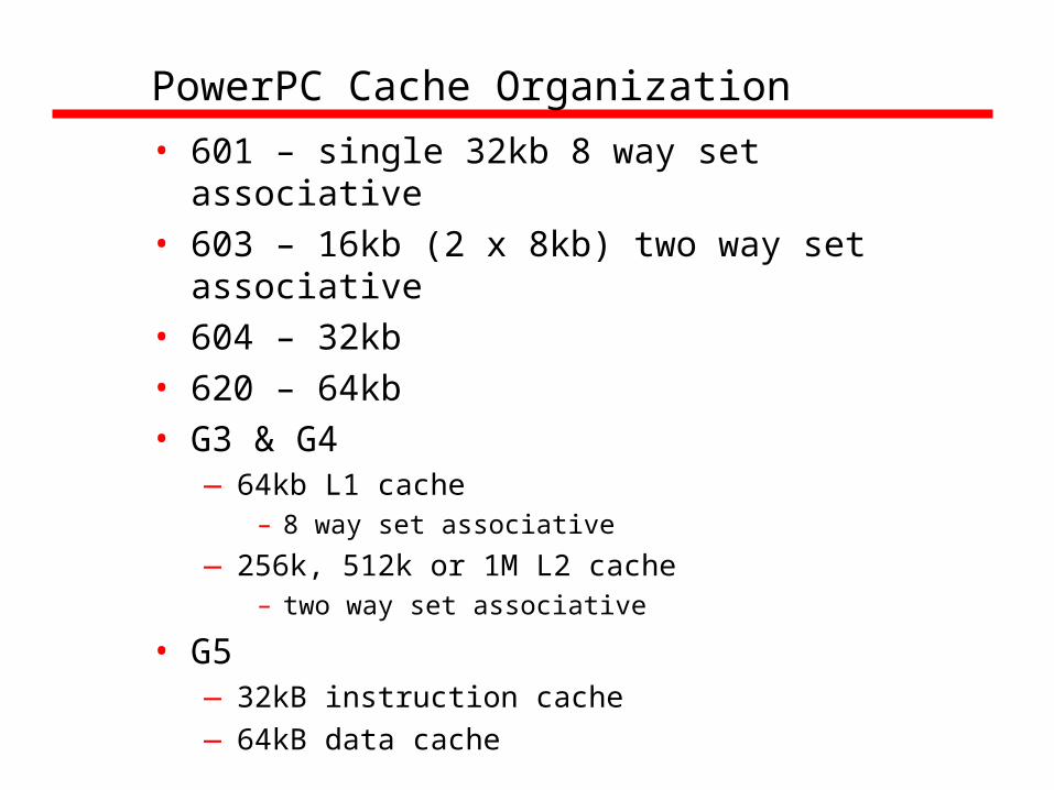
• 601 – single 32kb 8 way set associative• 603 – 16kb (2 x 8kb) two way set associative• 604 – 32kb• 620 – 64kb• G3 & G4
—64kb L1 cache– 8 way set associative
—256k, 512k or 1M L2 cache– two way set associative
• G5—32kB instruction cache—64kB data cache
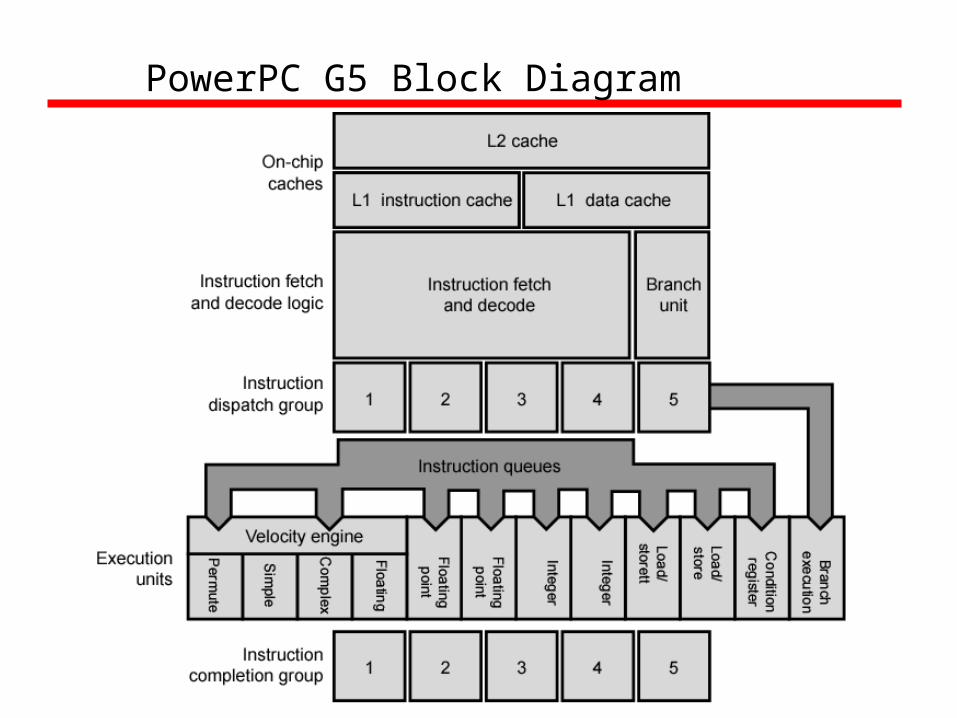
PowerPC G5 Block Diagram