Embed Size (px)
Citation preview
141403, CS2253 – COMPUTER ARCHITECTURE AND ORGANIZATION – NOTES
VASANTHA KUMAR.V AP/CSE 1
UNIT – I
BASIC STRUCTURE OF COMPUTERSFunctional units – Basic operational concepts – Bus structures – Performance and metrics –Instructions andinstruction sequencing – Hardware – Software Interface – Instruction set architecture – Addressing modes –RISC – CISC. ALU design – Fixed point and floating point operations.
1.1 EXPLAIN FUNCTIONAL UNIT OF A COMPUTER.
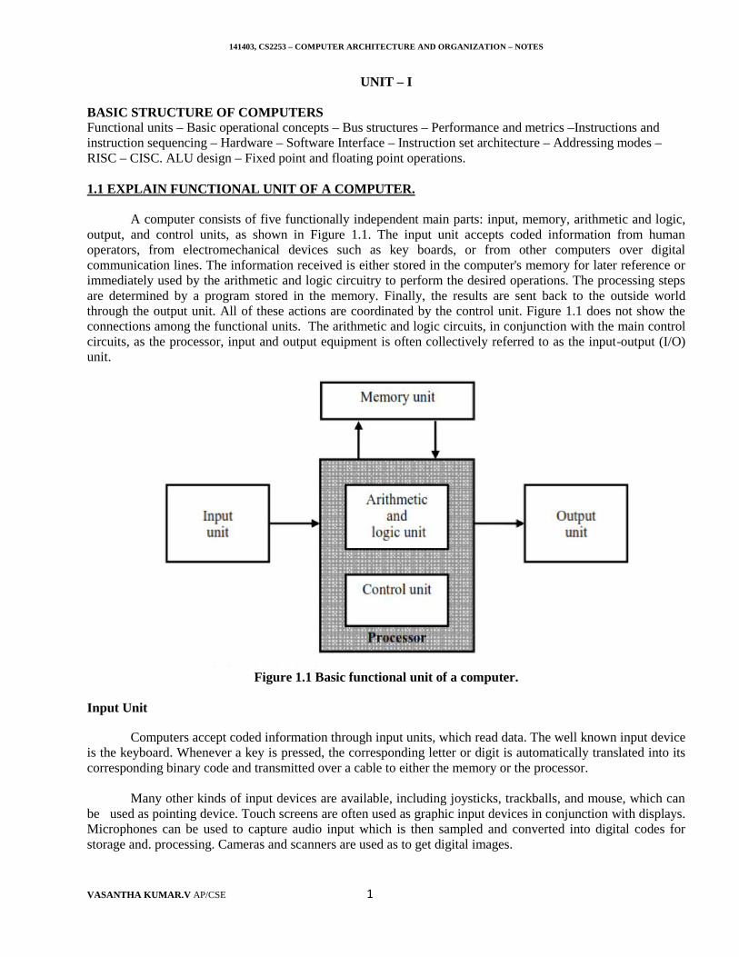
A computer consists of five functionally independent main parts: input, memory, arithmetic and logic,output, and control units, as shown in Figure 1.1. The input unit accepts coded information from humanoperators, from electromechanical devices such as key boards, or from other computers over digitalcommunication lines. The information received is either stored in the computer's memory for later reference orimmediately used by the arithmetic and logic circuitry to perform the desired operations. The processing stepsare determined by a program stored in the memory. Finally, the results are sent back to the outside worldthrough the output unit. All of these actions are coordinated by the control unit. Figure 1.1 does not show theconnections among the functional units. The arithmetic and logic circuits, in conjunction with the main controlcircuits, as the processor, input and output equipment is often collectively referred to as the input-output (I/O)unit.
Figure 1.1 Basic functional unit of a computer.
Input Unit
Computers accept coded information through input units, which read data. The well known input deviceis the keyboard. Whenever a key is pressed, the corresponding letter or digit is automatically translated into itscorresponding binary code and transmitted over a cable to either the memory or the processor.
Many other kinds of input devices are available, including joysticks, trackballs, and mouse, which canbe used as pointing device. Touch screens are often used as graphic input devices in conjunction with displays.Microphones can be used to capture audio input which is then sampled and converted into digital codes forstorage and. processing. Cameras and scanners are used as to get digital images.
141403, CS2253 – COMPUTER ARCHITECTURE AND ORGANIZATION – NOTES
VASANTHA KUMAR.V AP/CSE 2
Memory Unit
The function of the memory unit is to store programs and data. There are two classes of storage, calledprimary and secondary. Primary storage is a fast memory that operates at electronic speeds. Programs must bestored in the memory while they are being executed. The memory contains a large number of semiconductorstorage cells, each capable of storing one bit of information. These cells are rarely read or written as individualcells but instead are processed in groups of fixed size called words. The memory is organized so that thecontents of one word, containing n bits, can be stored or retrieved in one basic operation.
To provide easy access to any word in the memory, a distinct address is associated with each wordlocation. Addresses are numbers that identify successive locations. A given word is accessed by specifying itsaddress and issuing a control command that starts the storage or retrieval process. The number of bits in eachword is often referred to as the word length of the computer. Typical word lengths range from 16 to 64 bits. Thecapacity of the memory is one factor that characterizes the size of a computer.
Programs must reside in the memory during execution. Instructions and data can be written into thememory or read out under the controller of the processor. It is essential to be able to access any word location inthe memory as quickly as possible. Memory in which any location can be reached in a short and fixed amountof time after specifying its address is called random-access Memory (RAM). The time required to access oneword is called the Memory access time. This time is fixed, independent of the location of the word beingaccessed. It typically ranges from a few nanoseconds (ns) to about 100 ns for modem RAM units. The memoryof a computer is normally implemented as a Memory hierarchy of three or four levels of semiconductor RAMunits with different speeds and sizes. The small, fast, RAM units are called caches. They are tightly coupledwith the processor and are often contained on the same integrated circuit chip to achieve high performance. Thelargest and slowest unit is referred to as the main Memory.
Although primary storage is essential, it tends to be expensive. Thus additional, cheaper, secondarystorage is used when large amounts of data and many programs have to be stored, particularly for informationthat is access infrequently. A wide selection of secondary storage devices is available, including magnetic disksand tapes and optical disks
Arithmetic and Logic Unit.
Most computer operations are executed in the arithmetic and logic unit (ALU) of the processor.Consider a typical example: Suppose two numbers located in the memory are to be added. They are broughtinto the processor, and the actual addition is carried out by the ALU. The sum may then be stored in thememory or retained in the processor for immediate use.
Any other arithmetic or logic operation, for example, multiplication, division, or comparison ofnumbers, is initiated by bringing the required operands into the processor, where the operation is performed bythe ALU. When operands are brought into the processor, they are stored in high-speed storage elements calledregisters. Each register can store one word of data. Access times to registers are somewhat faster than accesstimes to the fastest cache unit in the memory hierarchy.
The control and the arithmetic and logic units are many times faster than other devices connected to acomputer system. This enables a single processor to control a number of external devices such as keyboards,displays, magnetic and optical disks, sensors, and mechanical controllers.
Output Unit
The output unit is the counterpart of the input unit. Its function is to send processed results to theoutside world. The most familiar example of such a device is a printer. Printers employ mechanical impactheads, inkjet streams, or photocopying techniques, as in laser printers, to perform the printing. It is possible to
141403, CS2253 – COMPUTER ARCHITECTURE AND ORGANIZATION – NOTES
VASANTHA KUMAR.V AP/CSE 3
produce printers capable of printing as many as 10,000 lines per minute. This is a tremendous speed for amechanical device but is still very slow compared to the electronic speed of a processor unit.
Monitors, Speakers, Headphones and projectors are also some of the output devices. Some units, suchas graphic displays, provide both an output function and an input function. The dual role of input and output ofsuch units are referred with single name as I/O unit in many cases. Speakers, Headphones and projectors aresome of the output devices. Storage devices such as hard disk, floppy disk, flash drives are also used for inputas well as output.
Control Unit
The memory, arithmetic and logic, and input and output 'units store and process information andperform input and output operations. The operation of these units must be coordinated in some way. This is thetask of the control unit. The control unit is effectively the nerve center that sends control signals to other unitsand senses their states.
I/O transfers, consisting of input and output operations, controlled by the instructions of I/O programsthat identify the devices involved and the information to be transferred. However, the actual timing signals thatgovern the transfers are generated by the control circuits. Timing signals are signals that determine when agiven action is to take place. Data transfers between the processor and the memory are also controlled by thecontrol unit through timing signals. It is reasonable to think of a control unit as a well-defined, physicallyseparate unit that interacts with other parts of the machine. In practice, however, this is seldom the case. Muchof the control circuitry is physically distributed throughout the machine. A large set of control lines (wires)carries the signals used for timing and synchronization of events in all units.
The operation of a computer can be summarized as follows:1. The computer accepts information in the form of programs and data through an input unit
and stores it in the memory.2. Information stored in the memory is fetched, under program control, into an arithmetic and
logic unit, where it is processed.3. Processed information leaves the computer through an output unit.4. All activities inside the machine are directed by the control unit.
x--------------------------------------------------------x--------------------------------------------------------x1.2 EXPLAIN BASIC OPERATIONS OF A COMPUTER. (Or)1.2 DISCUSS BASIC OPERATIONAL CONCEPTS.
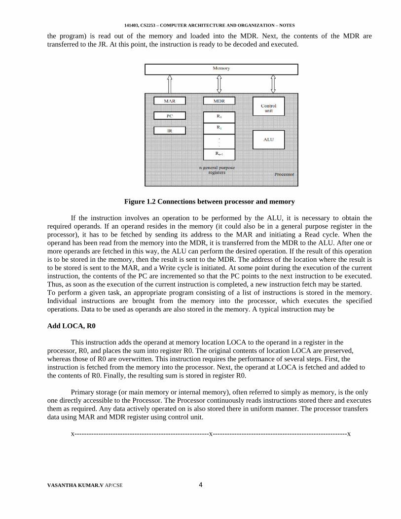
The processor contains arithmetic logic unit (ALU), control circuitry unit (CU) and a number ofregisters used for several different purposes. The instruction register (IR) holds the instruction that is currentlybeing executed. Its output is available to the control circuits, which generate the timing signals that control thevarious processing elements involved in executing the instruction. The program counter (PC) is anotherspecialized register. It keeps track of the execution of a program. "It contains the memory address of the nextinstruction to be fetched and executed. During the execution of an instruction, the contents of the PC areupdated to correspond to the address of the next instruction to be executed. It is customary to say that the PCpoints to the next instruction that is to be fetched from the memory. Besides the IR and PC, Figure 1.2 shows nGeneral-purpose registers, R0 through R n-1.
Finally, two registers facilitate communication with the memory. These are the memory address register(MAR) and the memory data register (MDR). The MAR holds the address of the location to be accessed. TheMDR contains the data to be written into or read out of the addressed location.
Let us now consider some typical operating steps. Programs reside in the memory and usuaJ1y get therethrough the input unit Execution of the program starts when the PC is set to point to the first instruction of theprogram. The contents of the PC are transferred to the MAR and a Read control signal is sent to the memory.After the time required to access the memory elapses, the addressed word (in this case, the first instruction of
141403, CS2253 – COMPUTER ARCHITECTURE AND ORGANIZATION – NOTES
VASANTHA KUMAR.V AP/CSE 4
the program) is read out of the memory and loaded into the MDR. Next, the contents of the MDR aretransferred to the JR. At this point, the instruction is ready to be decoded and executed.
Figure 1.2 Connections between processor and memory
If the instruction involves an operation to be performed by the ALU, it is necessary to obtain therequired operands. If an operand resides in the memory (it could also be in a general purpose register in theprocessor), it has to be fetched by sending its address to the MAR and initiating a Read cycle. When theoperand has been read from the memory into the MDR, it is transferred from the MDR to the ALU. After one ormore operands are fetched in this way, the ALU can perform the desired operation. If the result of this operationis to be stored in the memory, then the result is sent to the MDR. The address of the location where the result isto be stored is sent to the MAR, and a Write cycle is initiated. At some point during the execution of the currentinstruction, the contents of the PC are incremented so that the PC points to the next instruction to be executed.Thus, as soon as the execution of the current instruction is completed, a new instruction fetch may be started.To perform a given task, an appropriate program consisting of a list of instructions is stored in the memory.Individual instructions are brought from the memory into the processor, which executes the specifiedoperations. Data to be used as operands are also stored in the memory. A typical instruction may be
Add LOCA, R0
This instruction adds the operand at memory location LOCA to the operand in a register in theprocessor, R0, and places the sum into register R0. The original contents of location LOCA are preserved,whereas those of R0 are overwritten. This instruction requires the performance of several steps. First, theinstruction is fetched from the memory into the processor. Next, the operand at LOCA is fetched and added tothe contents of R0. Finally, the resulting sum is stored in register R0.
Primary storage (or main memory or internal memory), often referred to simply as memory, is the onlyone directly accessible to the Processor. The Processor continuously reads instructions stored there and executesthem as required. Any data actively operated on is also stored there in uniform manner. The processor transfersdata using MAR and MDR register using control unit.
x--------------------------------------------------------x--------------------------------------------------------x
141403, CS2253 – COMPUTER ARCHITECTURE AND ORGANIZATION – NOTES
VASANTHA KUMAR.V AP/CSE 5
1.3 EXPLAIN BUS STRUCTURE OF A COMPUTER.
Single bus structure
In computer architecture, a bus is a subsystem that transfers data between components inside acomputer, or between computers. Early computer buses were literally parallel electrical wires with multipleconnections, but Modern computer buses can use both parallel and bit serial connections.
Figure 1.3.1 Single bus structure
To achieve a reasonable speed of operation, a computer must be organized so that all its units canhandle one full word of data at a given time. When a word of data is transferred between units, all its bits aretransferred in parallel, that is, the bits are transferred simultaneously over many wires, or lines, one bit per line.A group of lines that serves as a connecting path for several devices is called a bus. In addition to the lines thatcarry the data, the bus must have lines for address and control purposes. The simplest way to interconnectfunctional units is to use a single bus, as shown in Figure 1.3.1. All units are connected to this bus. Because thebus can be used for only one transfer at a time, only two units can actively use the bus at any given time. Buscontrol lines are used to arbitrate multiple requests for use of the bus. The main virtue of the single-bus structureis it’s low cost and is flexibility for attaching peripheral" devices. Systems that contain multiple buses achievemore concurrency in operations by allowing two or more transfers to be carried out at the same time. This leadsto better performance but at an increased cost.
Figure 1.3.2 Bus interconnection scheme
The devices connected to a bus vary widely in their speed of operation. Some electromechanicaldevices, such as keyboards and printers are relatively slow. Other devises like magnetic or optical disks, areconsiderably faster. Memory and processor units operate at electronic speeds, making them the fastest parts of acomputer. Because all these devices must communicate with each other over a bus, an efficient transfer
141403, CS2253 – COMPUTER ARCHITECTURE AND ORGANIZATION – NOTES
VASANTHA KUMAR.V AP/CSE 6
mechanism that is not constrained by the slow devices and that can be used to smooth out the differences intiming among processors, memories, and external devices is necessary.
A common approach is to include buffer registers with the devices to hold the information duringtransfers. To illustrate this technique, consider the transfer of an encoded character from a processor to acharacter printer. The processor sends the character over the bus to the printer buffer. Since the buffer is anelectronic register, this transfer requires relatively little time. Once the buffer is loaded, the printer can startprinting without further intervention by the processor. The bus and the processor are no longer needed and canbe released for other activity. The printer continues printing the character in its buffer and is not available forfurther transfers until this process is completed. Thus, buffer registers smooth out timing differences amongprocessors, memories, and I/O devices. They prevent a high-speed processor from being locked to a slow I/Odevice during a sequence of data transfers. This allows the processor to switch rapidly from one device toanother, interweaving its processing activity with data transfers involving several I/O devices.
x--------------------------------------------------------x--------------------------------------------------------x
1.4 EXPLAIN PERFORMANCE AND METRICS
The most important measure of the performance of a computer is how quickly it can execute programs.The speed with which a computer executes programs is affected by the design of its hardware and its machinelanguage instructions. Because programs are usually written in a high-level language, performance is alsoaffected by the compiler that translates programs into machine language. For best performance, it is necessaryto design the compiler, the machine instruction set, and the hardware in a coordinated way. The operatingsystem overlaps processing, disk transfers, and printing for several programs to make the best possible use ofthe resources available. The total time required to execute the program is called elapsed time in operatingsystem. This elapsed time is a measure of the performance of the entire computer system. It is affected by thespeed of the processor, the disk, and the printer.
Cache MemoryJust as the elapsed time for the execution of a program depends on all units in a computer system, the
processor time depends on the hardware involved in the execution of individual machine instructions. Thishardware comprises the processor and the memory, which are usually connected by a bus, as shown in Figure1.3.1. The pertinent parts of this figure are repeated in Figure 1.4, including the cache memory as part of theprocessor unit. Let us examine the flow of program instructions and data between the memory and theprocessor. At the start of execution, all program instructions and the required data are stored in the mainmemory. As execution proceeds, instructions are fetched one by one over the bus into the processor, and a copyis placed in the cache. When the execution of an instruction calls for data located in the main memory, the dataare fetched and a copy is placed in the cache. Later, if the same instruction or data item is needed a second time,it is read directly from the cache.
Figure 1.4 Processor Cache
141403, CS2253 – COMPUTER ARCHITECTURE AND ORGANIZATION – NOTES
VASANTHA KUMAR.V AP/CSE 7
The processor and a relatively small cache memory can be fabricated on a single integrated circuit chip.The internal speed of performing the basic steps of instruction, processing on such chips is very high and isconsiderably faster than the speed at which instructions and data can be fetched from the main memory. Aprogram will be executed faster if the movement of instructions and data between the main memory and theprocessor is minimized, which is achieved by using the cache. For example, suppose a number of instructionsare executed repeatedly over a short period of time, as happens in a program loop. If these instructions areavailable in the cache, they can be fetched quickly during the period of repeated use.
Processor Clock
Processor circuits are controlled by a timing signal called a clock. The clock defines regular timeintervals, called clock cycles. To execute a machine instruction, the processor divides the action to beperformed into a sequence of basic steps, such that each step can be completed in one clock cycle. The length Pof one clock cycle is an important parameter that affects processor performance. Its inverse is the clock rate, R= 1/ P, which is measured in cycles per second. Processors used in today's personal computers and workstationshave clock rates that range from a few hundred million to over a billion cycles per second. In standard electricalengineering terminology, the term "cycles per second “is called hertz (Hz). The term "million" is denoted by theprefix Mega (M), and "billion" is denoted by the prefix Giga (G). Hence, 500 million cycles per second isusually abbreviated to 500 Megahertz (MHz), and 1250 million cycles per second is abbreviated to 1.25Gigahertz (GHz). The corresponding clock periods are 2 and 0.8 nanoseconds (ns), respectively.
Basic Performance Equation
Let T be the processor time required to execute a program that has been prepared in some high-levellanguage. The compiler generates a machine language object program that corresponds to the source program.
Assume that complete execution of the program requires the execution of N machine language instructions. Thenumber N is the actual number of instruction executions, and is not necessarily equal to the number of machine
instructions in the object program. Some instructions may be executed more than once, which is the case forinstructions inside a program loop. Others may not be executed at all, depending on the input data used.
Suppose that the average number of basic steps needed to execute one machine instruction is S, where eachbasic step is completed in one clock cycle. If the clock rate is R cycles per second, the program execution time
is
This is often referred to as the basic performance equation. The performance parameter T for anapplication program is much more important to the user than the individual values of the parameters N, S, or R.To achieve high performance, the computer designer must seek ways to reduce the value of T, which meansreducing N and S, and increasing R. The value of N is reduced if the source program is compiled into fewermachine instructions. The value of S is reduced if instructions have a smaller number of basic steps to performor if the execution of instructions is overlapped. Using a higher frequency clock increases the value or R, whichmeans that the time required to complete a basic execution step is reduced.
The N, S, and R are not independent parameters changing one may affect another. Introducing a newfeature in the design of a processor will lead to improved performance only if the overall result is to reduce thevalue of T. A processor advertised as having a 900-MHz clock does not necessarily provide better performancethan a 700-MHz processor because it may have a different value of S.
Pipelining and Superscalar Operation
Usually in sequential execution, the instructions are executed one after another. Hence, the value of S isthe total number of basic steps, or clock cycles, required to execute an instruction. A substantial improvement inperformance can be achieved by overlapping the execution of successive instructions, using a technique calledpipelining. Consider the instruction
141403, CS2253 – COMPUTER ARCHITECTURE AND ORGANIZATION – NOTES
VASANTHA KUMAR.V AP/CSE 8
Add Rl,R2,R3
This adds the contents of registers R 1 and R2, and places the sum into R3. The contents of Rl and R2are first transferred to the inputs of the ALU. After the add operation is performed, the sum is transferred to R3.The processor can read the next instruction from the memory while the addition oration is being performed.Then, if that instruction also uses the ALU, its operands can be transferred to the ALU inputs at the same timethat the result of the Add instruction is being transferred to R3. In the ideal case, if all instructions areoverlapped to the maximum degree possible, execution proceeds at the rate of one instruction completed in eachclock cycle. Individual instructions still require several clock cycles to complete. But, for the purpose ofcomputing T, the effective value of S is 1. The ideal va1ue S = 1 cannot be attained in practice for a variety ofreasons. However, pipelining increases the rate of executing instructions significantly and causes the effectivevalue of S to approach 1.
A higher degree of concurrency can be achieved if multiple instruction pipelines are implemented in theprocessor. This means that multiple functional units are used, creating parallel paths through which differentinstructions can be executed in parallel. With such an arrangement, it becomes possible to start the execution ofseveral instructions in every clock cycle. This mode of operation is called superscalar execution. If it can besustained for a long time during program execution, the effective value of S can be reduced to less than one. Ofcourse, parallel execution must preserve the logical correctness of programs, that is, the results produced mustbe the same as those produced by serial execution of program instructions. Many of today's high-performanceprocessors are designed to operate in this manner.
CLOCK RATE
There are two possibilities for increasing the clock rate, R. First, improving the integrated circuit (IC)technology makes logic circuits faster, which reduces the time needed to complete a basic step. This allows theclock period, P, to be reduced and the clock rate, R, to be increased. Second, reducing the amount of processingdone in one basic step also makes it possible to reduce the clock period, P. However, if the actions that have tobe performed by an instruction remain the same, the number of basic steps needed may increase. Increases inthe value of R that are entirely caused by improvements in IC technology affect all aspects of the processor'soperation equally with the exception of the time it takes to access the main memory. In the presence of a cache,the percentage of accesses to the main memory is small. Hence, much of the performance gain expected fromthe use of faster technology can be realized. The value of T will be reduced by the same factor as R is increasedbecause S and N are not affected.
Instruction Set: CISC and RISC
Simple instructions require a small number of basic steps to execute. Complex Instructions involve alarge number of steps. For a processor that has only simple instructions, a large number of instructions may beneeded to perform a given programming task. This could lead to a large value for N and a small value for S. Onthe other hand, if individual instructions perform more complex operations, fewer instructions will be needed,leading to a lower value of N and a larger value of S. It is not obvious if one choice is better than the other.A key consideration in comparing the two choices is the use of pipelining. We pointed out earlier that theeffective value of S in a pipelined processor is I close to 1 even though the number of basic steps per instructionmay be considerably larger. This seems to imply that complex instructions combined with pipelining wouldachieve the best performance. However, it is much easier to implement efficient pipelining in processors withsimple instruction sets. The suitability of the instruction set for pipelined execution is an important and oftendeciding consideration. The terms RISC and CISC refer to design principles and techniques. Reducedinstruction set computing (RISC), is a CPU design strategy based on the insight that simplified (as opposed tocomplex) instructions can provide higher performance if this simplicity enables much faster execution of eachinstruction. A complex instruction set computer (CISC) is a computer where single instructions can executeseveral low-level operations (such as a load from memory, an arithmetic operation, and a memory store) and/orare capable of multi-step operations or addressing modes within single instructions.
141403, CS2253 – COMPUTER ARCHITECTURE AND ORGANIZATION – NOTES
VASANTHA KUMAR.V AP/CSE 9
Compiler
A compiler translates a high-level language program into a sequence of machine instructions. To reduceN, we need to have a suitable machine instruction set and a compiler that makes good use of it. An optimizingcompiler takes advantage of various features of the target processor to reduce the product N x S, which is thetotal number of clock cycles needed to execute a program. The number of cycles is dependent not only on thechoice of instructions, but also on the order in which they appear in the program. The compiler may rearrangeprogram instructions to achieve better performance. Of course, such changes must not affect the result of thecomputation. Superficially, a compiler appears as a separate entity from the processor with which it is usedand may even be available from a different vendor. However, a high quality compiler must be closely linked tothe processor architecture. The compiler and the processor are often designed at the same time, with muchinteraction between the designers to achieve best results. The ultimate objective is to reduce the total number ofclock cycles needed to perform a required programming task.
Performance Equation
It is important to be able to assess the performance of a computer. Computer designers use performanceestimates to evaluate the effectiveness of new features. Manufacturers use performance indicators in themarketing process. Buyers use such data to choose among many available computer models. The previousdiscussion suggests that the only parameter that properly describes the performance of a computer is theexecution time, T, for the programs of interest. Despite the conceptual simplicity of Equation 1.1, computingthe value of T is not simple. Moreover, parameters such as the clock spee4 and various architectural features arenot reliable indicators of the expected performance. For these reasons, the computer community adopted theidea of measuring computer performance using benchmark programs. To make comparisons possible,standardized programs must be used. The performance measure is the time it takes a computer to execute agiven benchmark.
Initially, some attempts were made to create artificial programs that could be used as standardbenchmarks. But, synthetic programs do not properly predict performance obtained when real applicationprograms are nun .A nonprofit organization called System Performance Evaluation Corporation (SPEC) selectsand publishes representative application programs for different application domains, together with test resultsfor many commercially available computers. For general-purpose computers, a suite of benchmark programswas selected in 1989. It was modified somewhat and published in 1995 and again in 2000. For SPEC2000, thereference computer is an Ultra SPARCI0 workstation with a 300-MHz UltraSPARC-III processor.The SPEC rating is computed as follows
Thus a SPEC rating of 50 means that the computer under test is 50 times as fast as the Ultra SPARC I0 for thisparticular benchmark. The test is repeated for all the programs in the SPEC suite, and the geometric mean of theresults is computed. Let SPEC i be the rating for program i in the suite. The overall SPEC rating for thecomputer is given by
x--------------------------------------------------------x--------------------------------------------------------x
141403, CS2253 – COMPUTER ARCHITECTURE AND ORGANIZATION – NOTES
VASANTHA KUMAR.V AP/CSE 10
1.5 EXPLAIN INSTRUCTION AND INSTRUCTION SEQUENCING
A computer program consist of a sequence of small steps, such as adding two numbers, testing for aparticular condition, reading a character from the keyboard, or sending a character to be displayed on a displayscreen.
A computer must have instructions capable of performing four types of operations:· Data transfers between the memory and the processor registers· Arithmetic and logic operations on data· Program sequencing and control· I/O transfers
In general, the information is transferred from one location to another in a computer. Possible locationsfor such transfers are memory locations, processor registers, or registers in the I/O subsystem.
For example, Names for the addresses of memory locations may be LOC, PLACE, A, VAR2; processor registernames may be RO, R5; and I/O register names may be DATAIN, OUTSTATUS, and so on. The contents of alocation are denoted by placing square brackets around the name of the location. Thus, the expression
means that the contents of memory location LOC are transferred into processor register R1.
As another example, consider the operation that adds the contents of registers R1 and R2,and thenplaces their sum into register R3. This action is indicated as
This type of notation is known as Register Transfer Notation (RTN). .Note that the right hand side of anRTN expression always denotes a value and the left-hand side is the name of a location where the value is to beplaced, overwriting the old contents of that location.
Assembly Transfer Notation
The another type of notation to represent machine instructions and programs is assembly transfernotation. For example, an instruction that causes the transfer described above, from memory location LOC toprocessor register RI, is specified by the statement.
Move LOC,RlThe contents of LOC are unchanged by the execution of this instruction, but the old contents of register R1are overwritten. The second example of adding two numbers contained in processor registers Rl and R2 andplacing their sum in R3 can be specified by the assembly language statement
Add RI,R2,R3
Basic Instruction Types
Instruction types are classified based on the number of operands used in instructions. They are:(i). Three - Address Instruction,(ii). Two - Address Instruction,(iii). One - Address Instruction, and(iv). Zero - Address Instruction.Consider a high level language program command, which adds two variables A and B, and assignthe sum in third variable C.
C = A + B ;To carry out this action, the contents of memory locations A and B are fetched from the memory and transferredinto the processor where their Sum is computed. This result is then sent back to the memory and stored inlocation C.
141403, CS2253 – COMPUTER ARCHITECTURE AND ORGANIZATION – NOTES
VASANTHA KUMAR.V AP/CSE 11
C ← [A] + [B]Example: Add two variables A and B, and assign the sum in third variable C
(i). Three - Address Instruction
The general instruction format is: Operation Source1,Source2,DestinationSymbolic add instruction: ADD A,B,COperands A and B are called the source operands, C is called Destination operand, and Add is the
operation to be performed on the operands. If k bits are needed to specify the memory address of each operand,the encoded form of the above instruction must contain 3k bits for addressing purposes in addition to the bitsneeded to denote the Add operation. For a modem processor with a 32-bit address space, a 3-address instructionis too large to fit in one word for a reasonable word length. Thus, a format that allows multiple words to be usedfor a single instruction would be needed to represent an instruction of this type. An alternative approach is touse a sequence of simpler instructions to perform the same task, with each instruction having only one or twooperands.
(ii). Two - Address Instruction
The general instruction format is: Operation Source, DestinationSymbolic add instruction: MOVE B,C
ADD A,CAn Add instruction of this type is ADD A,B which performs the operation B ← [A] + [B] When the
sum is calculated, the result is sent to the memory and stored in location B, replacing the original contents ofthis location. This means that operand B is both a source and a destination .A single two-address instructioncannot be used to solve our original problem, which is to add the contents of locations A and B, withoutdestroying either of them, and to place the sum in location C. The problem can be solved by using another two-address instruction that copies the contents of one memory location into another. Such an instruction is MoveB,C which performs the operation C ← [B], leaving the contents of location B unchanged. The word "Move" isa misnomer here; it should be "Copy." However, this instruction name is deeply entrenched in computernomenclature. The operation C ← [A] + [B] can now be performed by the two instruction sequence
Move B,CAdd A,C
Even two-address instructions will not normally fit into one word for usual word lengths and addresssizes. Another possibility is to have machine instructions that specify only one memory operand. when a secondoperand is needed, as in the case of an Add instruction, it is understood implicitly to be in a unique location. Aprocessor register, usually called the accumulator, may be used for this purpose. Thus, the one-addressinstruction
(iii). One - Address Instruction
The general instruction format is: Operation operandSymbolic add instruction: LOAD A
ADD BSTORE C
ADD A means the following: Add the contents of memory location A to the contents of the accumulatorregister and place the sum back into the accumulator. Let us also introduce the oneaddress instructions
Load A and Store AThe Load instruction copies the contents of memory location A into the Accumulator, and the Store
instruction copies the contents of the accumulator into memory location A. Using only one-address instructions,the operation C ← [A] + [B] can be performed by executing the sequence of instructions
Load A, Add B, Store CThe operand specified in the instruction may be a source or a destination, depending on the instruction.
In the Load instruction, address A specifies the source operand, and the destination location, the accumulator, is
141403, CS2253 – COMPUTER ARCHITECTURE AND ORGANIZATION – NOTES
VASANTHA KUMAR.V AP/CSE 12
implied. On the other hand, C denotes the destination location in the Store instruction, whereas the source, theaccumulator, is implied.
Instruction Execution and Straight Line Sequencing
To perform a particular task on the computer, it is programmer’s job to select and write appropriateinstructions one after other, i.e. programmer has to write instructions in a proper sequence. This job of theprogrammer is known as instruction sequencing. The instructions written in a proper sequence to execute aparticular task is called program.
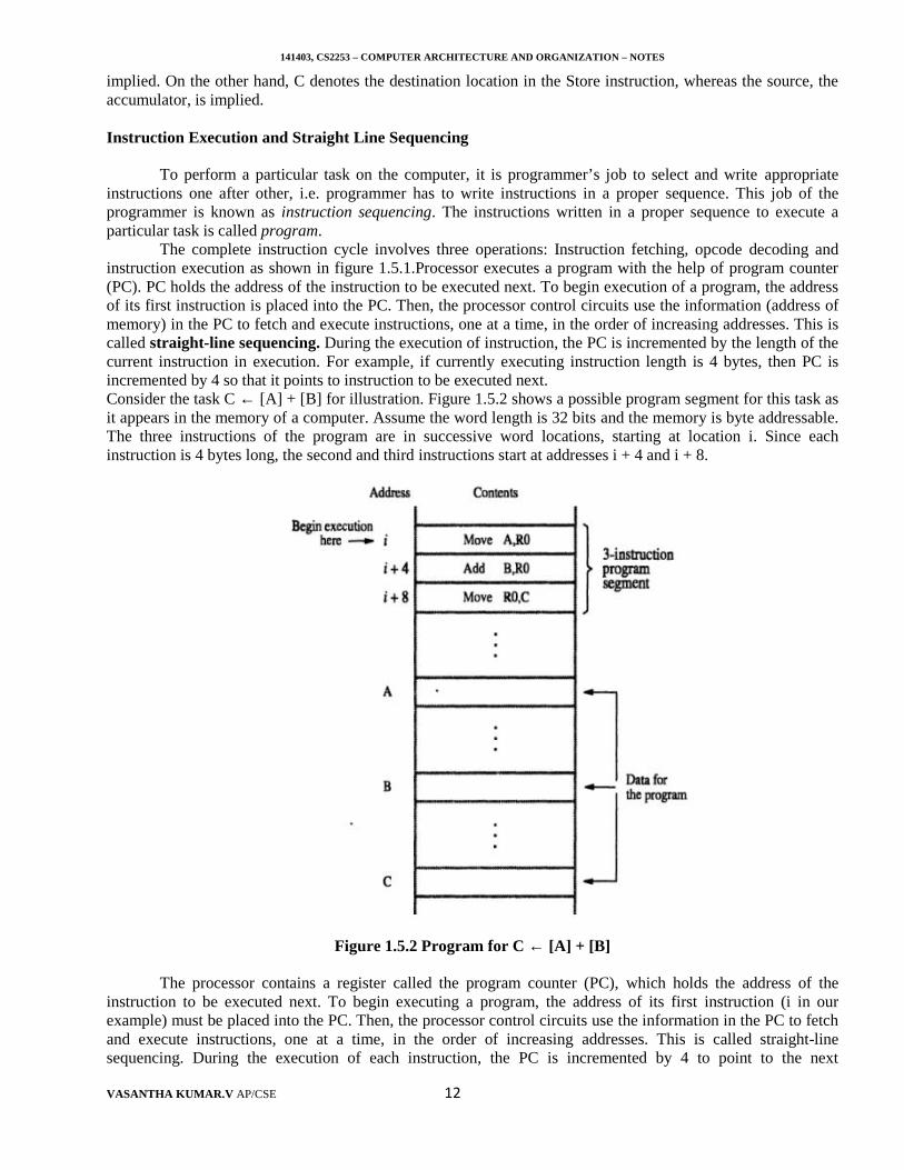
The complete instruction cycle involves three operations: Instruction fetching, opcode decoding andinstruction execution as shown in figure 1.5.1.Processor executes a program with the help of program counter(PC). PC holds the address of the instruction to be executed next. To begin execution of a program, the addressof its first instruction is placed into the PC. Then, the processor control circuits use the information (address ofmemory) in the PC to fetch and execute instructions, one at a time, in the order of increasing addresses. This iscalled straight-line sequencing. During the execution of instruction, the PC is incremented by the length of thecurrent instruction in execution. For example, if currently executing instruction length is 4 bytes, then PC isincremented by 4 so that it points to instruction to be executed next.Consider the task C ← [A] + [B] for illustration. Figure 1.5.2 shows a possible program segment for this task asit appears in the memory of a computer. Assume the word length is 32 bits and the memory is byte addressable.The three instructions of the program are in successive word locations, starting at location i. Since eachinstruction is 4 bytes long, the second and third instructions start at addresses i + 4 and i + 8.
Figure 1.5.2 Program for C ← [A] + [B]
The processor contains a register called the program counter (PC), which holds the address of theinstruction to be executed next. To begin executing a program, the address of its first instruction (i in ourexample) must be placed into the PC. Then, the processor control circuits use the information in the PC to fetchand execute instructions, one at a time, in the order of increasing addresses. This is called straight-linesequencing. During the execution of each instruction, the PC is incremented by 4 to point to the next
141403, CS2253 – COMPUTER ARCHITECTURE AND ORGANIZATION – NOTES
VASANTHA KUMAR.V AP/CSE 13
instruction. Thus, after the Move instruction at location i + 8 is executed, the PC contains the value i + 12,which is the address of the first instruction of the next program segment. Executing a given instruction is a two-phase procedure. In the first phase, called instruction fetch, the instruction is fetched from the memory locationwhose address is in the PC. This instruction is placed in the instruction register (IR) in the processor. At the startof the second phase, called instruction execute, the instruction in IR is examined to determine which operationis to be performed. The specified operation is then performed by the processor. This often involves fetchingoperands from the memory or from processor registers, performing an arithmetic or logic operation, and storingthe result in the destination location. At some point during this two-phase procedure, the contents of the PC areadvanced to point to the next instruction. When the execute phase of an instruction is completed, the PCcontains the address of the next instruction, and a new instruction fetch phase can begin. In most processors, theexecute phase itself is divided into asmall number of distinct phases corresponding to fetching operands,performing the operation, and storing the result.
Branching
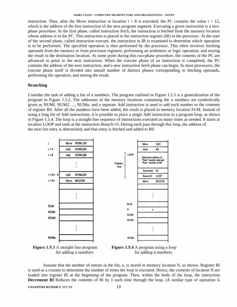
Consider the task of adding a list of n numbers. The program outlined in Figure 1.5.3 is a generalization of theprogram in Figure 1.5.2. The addresses of the memory locations containing the n numbers are symbolicallygiven as NUMl, NUM2, ..., NUMn, and a separate Add instruction is used to add each number to the contentsof register R0. After all the numbers have been added, the result is placed in memory location SUM. Instead ofusing a long list of Add instructions, it is possible to place a single Add instruction in a program loop, as shownin Figure 1.5.4. The loop is a straight-line sequence of instructions executed as many times as needed. It starts atlocation LOOP and ends at the instruction Branch>O. During each pass through this loop, the address ofthe next list entry is determined, and that entry is fetched and added to R0.
Assume that the number of entries in the list, n, is stored in memory location N, as shown. Register Rlis used as a counter to determine the number of times the loop is executed. Hence, the contents of location N areloaded into register Rl at the beginning of the program. Then, within the body of the loop, the instructionDecrement Rl Reduces the contents of Rl by 1 each time through the loop. (A similar type of operation is
141403, CS2253 – COMPUTER ARCHITECTURE AND ORGANIZATION – NOTES
VASANTHA KUMAR.V AP/CSE 14
performed by an Increment instruction, which adds 1 to its operand.) Execution of the loop is repeated as longas the result of the decrement operation is greater than zero. This type of instruction loads a new value into theprogram counter. As a result, the processor fetches and executes the instruction at this new address, called thebranch target, instead of the instruction at the location that follows the branch instruction in sequential addressorder. A conditional branch instruction causes a branch only if a specified condition is satisfied. If thecondition is not satisfied, the PC is incremented in the normal way, and the next instruction in sequentialaddress order is fetched and executed.
Condition Codes
The processor keeps track of information about the results of various operations for use by subsequentconditional branch instructions. This is accomplished by recording the required information in individual bits,often called condition code flags. These flags are usually grouped together in a special processor register calledthe condition code register or status register. Individual condition code flags are set to 1 or cleared to 0,depending on the outcome of the operation performed.
Four commonly used flags are
N (negative) Set to 1 if the result is negative; otherwise, cleared to 0Z (zero) Set to 1 if the result is 0; otherwise, cleared to 0V (overflow) Set to 1 if arithmetic overflow occurs; otherwise, cleared to 0C (carry) Set to 1 if a carry-out results from the operation; otherwise, cleared to 0
The N and Z flags indicate whether the result of an arithmetic or logic operation is negative or zero. The N andZ flags may also be affected by instructions that transfer data, such as Move, Load, or Store. This makes itpossible for a later conditional branch instruction to cause a branch based on the sign and value of the operandthat was moved. Some computers also provide a special Test instruction that examines a value in a register or inthe memory and sets or clears the N and Z flags accordingly.
Generation of Memory Addresses
Different addressing modes give rise to the need for flexible ways to specify the address of an operand.The instruction set of a computer typically provides a number of such methods, called addressing modes. Whilethe details differ from one computer to another, the underlying concepts are the same.
x--------------------------------------------------------x--------------------------------------------------------x
1.6 DISCUSS HARDWARE – SOFTWARE INTERFACE
HardwareComputer hardware is the collection of physical elements that comprise a computer system. Example
Processor, memory, hard disk, floppy disk, keyboard, mouse, monitors, printers and so on.
SoftwareComputer software, or just software, is a collection of computer programs and related data that provides
the instructions for telling a computer what to do and how to do it. In other words, software is a conceptualentity which is a set of computer programs, procedures, and associated documentation concerned with theoperation of a data processing system. We can also say software refers to one or more computer programs anddata held in the storage of the computer for some purposes. In other words software is a set of programs,procedures, algorithms and its documentation. Program software performs the function of the program itimplements, either by directly providing instructions to the computer hardware or by serving as input to anotherpiece of software. The term was coined to contrast to the old term hardware (meaning physical devices). Incontrast to hardware, software "cannot be touched". Software is also sometimes used in a more narrow sense,meaning application software only.
141403, CS2253 – COMPUTER ARCHITECTURE AND ORGANIZATION – NOTES
VASANTHA KUMAR.V AP/CSE 15
System software
System software provides the basic functions for computer usage and helps run the computer hardwareand system. It includes a combination of the following:
1. Device drivers:A device driver or software driver is a computer program allowing higher-level computer programs to interactwith a hardware device.
2. Operating systems:An operating system (OS) is a set of programs that manage computer hardware resources and provide commonservices for application software. The operating system is the most important type of system software in acomputer system. A user cannot run an application program on the computer without an operating system,unless the application program is self booting. The main functions of an OS are Device management, Storagemanagement, User interface, Memory management and Processor management
3. Servers:A server is a computer program running to serve the requests of other programs, the "clients". Thus, the "server"performs some computational task on behalf of "clients". The clients either run on the same computer orconnect through the network.
4. Utilities:
Utility software is system software designed to help analyze, configure, optimize or maintain a computer. Asingle piece of utility software is usually called a utility or tool. Utility software usually focuses on how thecomputer infrastructure (including the computer hardware, operating system, application software and datastorage) operates.
5. Window systems:A windowing system (or window system) is a component of a graphical user interface (GUI), and morespecifically of a desktop environment, which supports the implementation of window managers, and providesbasic support for graphics hardware, pointing devices such as mice, and keyboards. The mouse cursor is alsogenerally drawn by the windowing system. System software is responsible for managing a variety ofindependent hardware components, so that they can work together harmoniously. Its purpose is to unburden theapplication software programmer from the often complex details of the particular computer being used,including such accessories as communications devices, printers, device readers, displays and keyboards, andalso to partition the computer's resources such as memory and processor time in a safe and stable manner.
Programming software
Programming software usually provides tools to assist a programmer in writing computer programs, andsoftware using different programming languages in a more convenient way. The tools include:
1. Compilers:A compiler is a computer program (or set of programs) that transforms source code written in a
programming language (the source language) into another computer language (the target language, often havinga binary form known as object code). The most common reason for wanting to transform source code is tocreate an executable program. The name "compiler" is primarily used for programs that translate source codefrom a high level programming language to a lower level language (e.g., assembly language or machine code).If the compiled program can run on a computer whose CPU or operating system is different from the one onwhich the compiler runs, the compiler is known as a cross-compiler. A program that translates from a low levellanguage to a higher level one is a compiler. A compiler is likely to perform many or all of the following
141403, CS2253 – COMPUTER ARCHITECTURE AND ORGANIZATION – NOTES
VASANTHA KUMAR.V AP/CSE 16
operations: lexical analysis, preprocessing, parsing, semantic analysis (Syntax-directed translation), codegeneration, and code optimization.
2. Debuggers:A debugger or debugging tool is a computer program that is used to test and debug other programs (the
"target" program). The code to be examined might alternatively be running on an instruction set simulator (ISS),a technique that allows great power in its ability to halt when specific conditions are encountered but which willtypically be somewhat slower than executing the code directly on the appropriate (or the same) processor. Somedebuggers offer two modes of operation - full or partial simulation, to limit this impact.
3. Interpreters:An interpreter normally means a computer program that executes Program by converting source code to
object code line by line.
4. Linkers:A linker or link editor is a program that takes one or more objects generated by a compiler and
combines them into a single executable program.
5. Text editors:A text editor is a type of program used for editing plain text files.Text editors are often provided with
operating systems or software development packages, and can be used to change configuration files andprogramming language source code.An Integrated development environment (IDE) is a single application thatattempts to manage all these functions.
Application software
Application software is developed to perform in any task that benefits from computation. It is abroad category, and encompasses software of many kinds, including the internet browser beingused to display this page. This category includes:
Business softwareComputer-aided designDatabasesDecision making software
Hardware – Software Interface
It is an interface tool and it to a point of interaction between components, and is applicable at the levelof both hardware and software. This allows a component, whether a piece of hardware such as a graphics cardor a piece of software such as an Internet browser, to function independently while using interfaces tocommunicate with other components via an input/output system and an associated protocol.
All Device drivers, Operating systems, Servers, Utilities, Window systems, Compilers, Debuggers,Interpreters, Linkers and Text editors are considered as Harware – Software Interfaces.
x--------------------------------------------------------x--------------------------------------------------------x
1.7 EXPLAIN VARIOUS ADDRESSING MODES
The different ways in which the location of an operand is specified in an instruction are referred to asaddressing modes.
1. Register addressing mode - The operand is the contents of a processor register; the name (address) of theregister is given in the instruction.
141403, CS2253 – COMPUTER ARCHITECTURE AND ORGANIZATION – NOTES
VASANTHA KUMAR.V AP/CSE 17
Example: MOVE R1,R2This instruction copies the contents of register R2 to R1.
2. Absolute addressing mode - The operand is in a memory location; the address of this location is givenexplicitly in the instruction. (In some assembly languages, this mode is called Direct.
Example: MOVE LOC,R2This instruction copies the contents of memory location of LOC to register R2.
3. Immediate addressing mode - The operand is given explicitly in the instruction.Example: MOVE #200 , R0
The above statement places the value 200 in the register R0. A common convention is to use the sharp sign (#)in front of the value to indicate that this value is to be used as an immediate operand.
4. Indirect addressing mode - The effective address of the operand is the contents of a register or memorylocation whose address appears in the instruction.
Example Add (R2),R0Register R2 is used as a pointer to the numbers in the list, and the operands are accessed indirectly
through R2. The initialization section of the program loads the counter value n from memory location N into Rland uses the Immediate addressing mode to place the address value NUM 1, which is the address of the firstnumber in the list, into R2.
5. Index mode - The effective address of the operand is generated by adding a constant value to the contents ofa register. The register used may be either a special register provided for this purpose, or, more commonly; itmay be anyone of a set of general-purpose registers in the processor. In either case, it is referred to as an indexregister. We indicate the Index mode symbolically as X(Ri). Where X denotes the constant value contained inthe instruction and Ri is the name of the register involved. The effective address of the operand is given byEA = X + [Ri]. The contents of the index register are not changed in the process of generating the effectiveaddress.
Relative Addressing
We have defined the Index mode using general-purpose processor registers. A useful version of thismode is obtained if the program counter, PC, is used instead of a general purpose register. Then, X(PC) can beused to address a memory location that is X bytes away from the location presently pointed to by the programcounter. Since the addressed location is identified ''relative'' to the program counter, which always identifies thecurrent execution point in a program, the name Relative mode is associated with this type of addressing.
6.Relative mode - The effective address is determined by the Index mode using the program counter in place ofthe general-purpose register Ri.
This mode can be used to access data operands. But, its most common use is to specify the targetaddress in branch instructions. An instruction such as Branch>O LOOP causes program execution to go to thebranch target location identified by the name LOOP if the branch condition is satisfied. This location can becomputed by specifying it as an offset from the current value of the program counter. Since the branch targetmay be either before or after the branch instruction, the offset is given as a signed number.
7. Autoincrement mode - The effective address of the operand is the contents of a register specified in theinstruction. After accessing the operand, the contents of this register are automatically incremented to point tothe next item in a list. We denote the Autoincrement mode by putting the specified register in parentheses, toshow that the contents of the register are used as the effective address, followed by a plus sign to indicate thatthese contents are to be incremented after the operand is accessed. Thus, the Autoincrement mode is written as(Ri) +As a companion for the Autoincrement mode, another useful mode accesses the items of a list in the reverseorder:
141403, CS2253 – COMPUTER ARCHITECTURE AND ORGANIZATION – NOTES
VASANTHA KUMAR.V AP/CSE 18
8. Autodecrement mode - The contents of a register specified in the instruction is first automaticallydecremented and is then used as the effective address of the operand. We denote the Autodecrement mode byputting the specified register in parentheses, preceded by a minus sign to indicate that the contents of theregister are to be decremented before being used as the effective address. Thus, we write - (Ri)
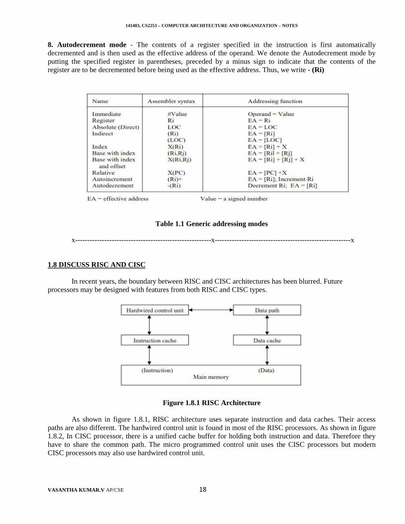
Table 1.1 Generic addressing modes
x--------------------------------------------------------x--------------------------------------------------------x
1.8 DISCUSS RISC AND CISC
In recent years, the boundary between RISC and CISC architectures has been blurred. Futureprocessors may be designed with features from both RISC and CISC types.
Figure 1.8.1 RISC Architecture
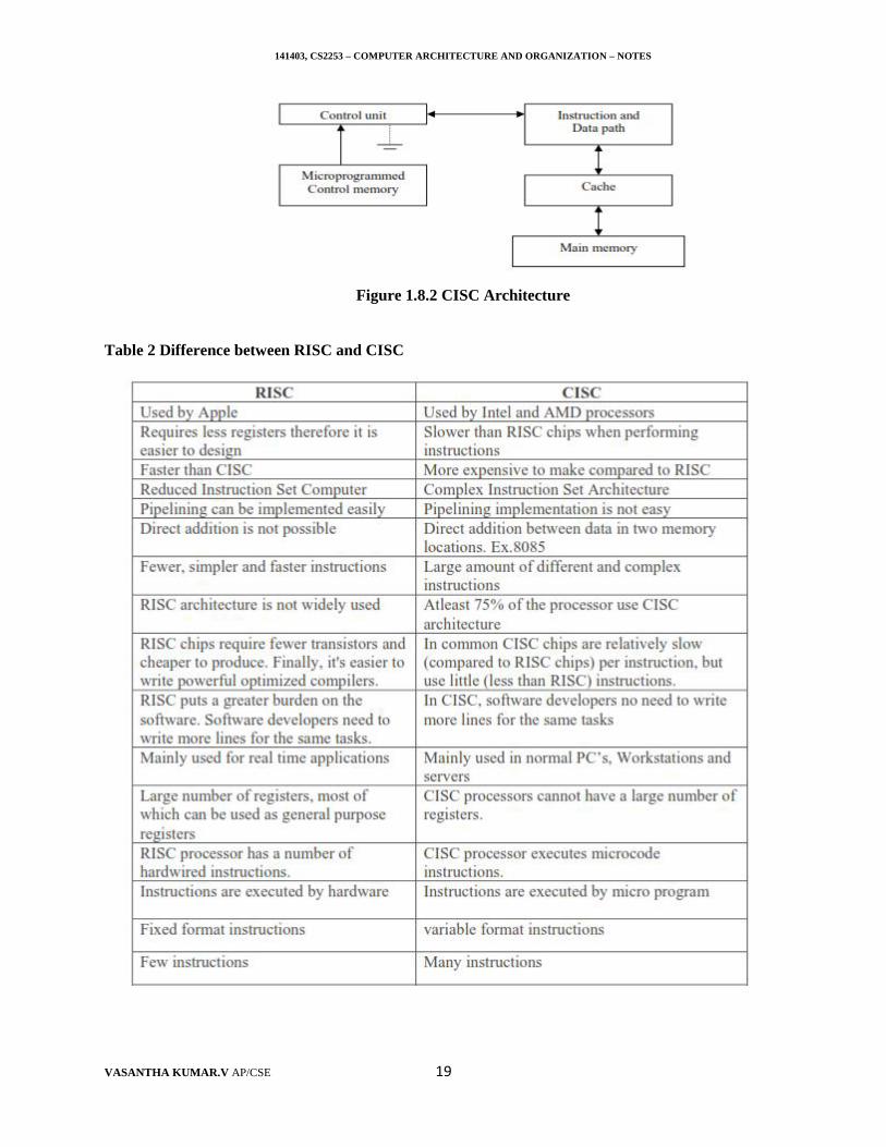
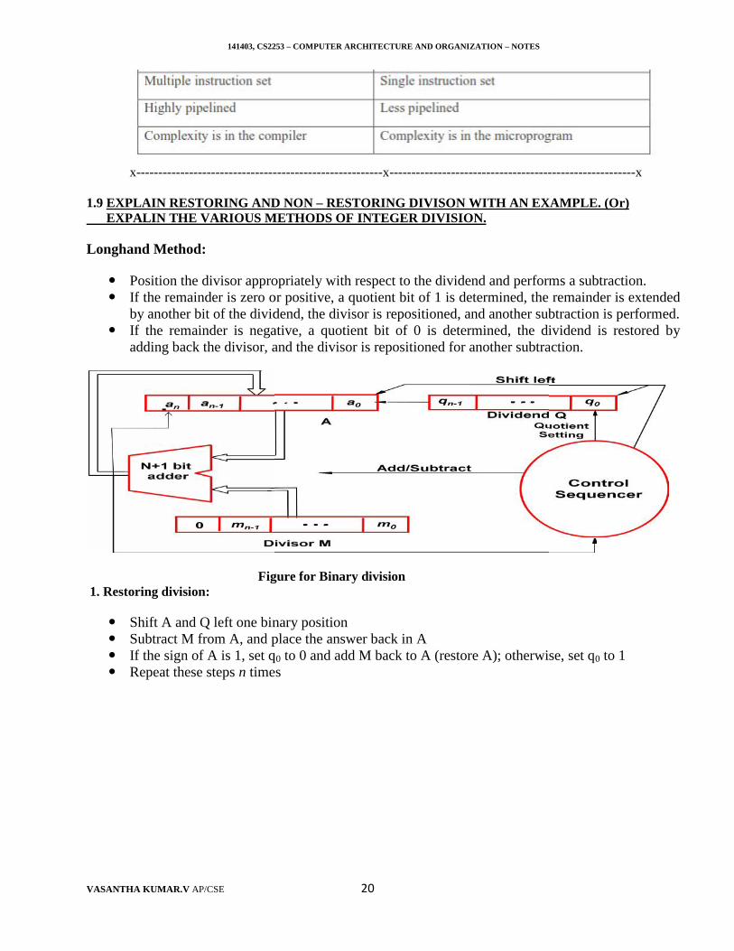
As shown in figure 1.8.1, RISC architecture uses separate instruction and data caches. Their accesspaths are also different. The hardwired control unit is found in most of the RISC processors. As shown in figure1.8.2, In CISC processor, there is a unified cache buffer for holding both instruction and data. Therefore theyhave to share the common path. The micro programmed control unit uses the CISC processors but modernCISC processors may also use hardwired control unit.
141403, CS2253 – COMPUTER ARCHITECTURE AND ORGANIZATION – NOTES
VASANTHA KUMAR.V AP/CSE 19
Figure 1.8.2 CISC Architecture
Table 2 Difference between RISC and CISC
141403, CS2253 – COMPUTER ARCHITECTURE AND ORGANIZATION – NOTES
VASANTHA KUMAR.V AP/CSE 20
x--------------------------------------------------------x--------------------------------------------------------x
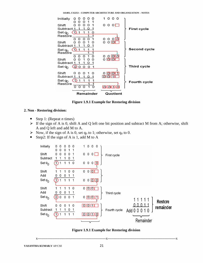
1.9 EXPLAIN RESTORING AND NON – RESTORING DIVISON WITH AN EXAMPLE. (Or)EXPALIN THE VARIOUS METHODS OF INTEGER DIVISION.
Longhand Method:
Position the divisor appropriately with respect to the dividend and performs a subtraction. If the remainder is zero or positive, a quotient bit of 1 is determined, the remainder is extended
by another bit of the dividend, the divisor is repositioned, and another subtraction is performed. If the remainder is negative, a quotient bit of 0 is determined, the dividend is restored by
adding back the divisor, and the divisor is repositioned for another subtraction.
Figure for Binary division1. Restoring division:
Shift A and Q left one binary position Subtract M from A, and place the answer back in A If the sign of A is 1, set q0 to 0 and add M back to A (restore A); otherwise, set q0 to 1 Repeat these steps n times
141403, CS2253 – COMPUTER ARCHITECTURE AND ORGANIZATION – NOTES
VASANTHA KUMAR.V AP/CSE 20
x--------------------------------------------------------x--------------------------------------------------------x
1.9 EXPLAIN RESTORING AND NON – RESTORING DIVISON WITH AN EXAMPLE. (Or)EXPALIN THE VARIOUS METHODS OF INTEGER DIVISION.
Longhand Method:
Position the divisor appropriately with respect to the dividend and performs a subtraction. If the remainder is zero or positive, a quotient bit of 1 is determined, the remainder is extended
by another bit of the dividend, the divisor is repositioned, and another subtraction is performed. If the remainder is negative, a quotient bit of 0 is determined, the dividend is restored by
adding back the divisor, and the divisor is repositioned for another subtraction.
Figure for Binary division1. Restoring division:
Shift A and Q left one binary position Subtract M from A, and place the answer back in A If the sign of A is 1, set q0 to 0 and add M back to A (restore A); otherwise, set q0 to 1 Repeat these steps n times
141403, CS2253 – COMPUTER ARCHITECTURE AND ORGANIZATION – NOTES
VASANTHA KUMAR.V AP/CSE 21
Figure 1.9.1 Example for Restoring division
2. Non - Restoring division:
Step 1: (Repeat n times) If the sign of A is 0, shift A and Q left one bit position and subtract M from A; otherwise, shift
A and Q left and add M to A. Now, if the sign of A is 0, set q0 to 1; otherwise, set q0 to 0. Step2: If the sign of A is 1, add M to A
Figure 1.9.1 Example for Restoring division
x--------------------------------------------------------x--------------------------------------------------------x
141403, CS2253 – COMPUTER ARCHITECTURE AND ORGANIZATION – NOTES
VASANTHA KUMAR.V AP/CSE 22
1.10. EXPLAIN THE ARITHEMATIC OPERATION ON FLOATING POINT NUMBER
ADD/SUBTRACT RULES:
Choose the number with the smaller exponent. Shift its mantissa right until the exponents of both the numbers are equal. Add or subtract the mantissas. Determine the sign of the result. Normalize the result if necessary and truncate/round to the number of mantissa bits.
MULTIPLY RULE:
Add the exponents. Subtract the bias. Multiply the mantissas and determine the sign of the result. Normalize the result (if necessary). Truncate/round the mantissa of the result.
DIVIDE RULE:
Subtract the exponents Add the bias. Divide the mantissas and determine the sign of the result. Normalize the result if necessary. Truncate/round the mantissa of the result.
x--------------------------------------------------------x--------------------------------------------------------x
1.11. WRITE A SHORT NOTE ON GUARD BIT AND TRUNCATION
GUARD BIT:
While adding two floating point numbers with 24-bit mantissas, we shift the mantissa of thenumber with the smaller exponent to the right until the two exponents are equalized. This implies thatmantissa bits may be lost during the right shift (that is, bits of precision may be shifted out of themantissa being shifted). To prevent this, floating point operations are implemented by keeping guardbits, that is, extra bits of precision at the least significant end of the mantissa. The arithmetic on themantissas is performed with these extra bits of precision. After an arithmetic operation, the guardedmantissas are:
- Normalized (if necessary)- Converted back by a process called truncation/rounding to a 24-bit mantissa.
TRUNCATION AND ROUNDING:
Straight chopping:
The guard bits (excess bits of precision) are dropped.
Von Neumann rounding:
141403, CS2253 – COMPUTER ARCHITECTURE AND ORGANIZATION – NOTES
VASANTHA KUMAR.V AP/CSE 23
If the guard bits are all 0, they are dropped.
However, if any bit of the guard bit is a 1, then the LSB of the retained bit is set to 1.
Rounding:
If there is a 1 in the MSB of the guard bit then a 1 is added to the LSB of the retainedbits.
Rounding is evidently the most accurate truncation method.
However,
Rounding requires an addition operation.
Rounding may require a renormalization, if the addition operation de-normalizes thetruncated number.
IEEE uses the rounding method.
x--------------------------------------------------------x--------------------------------------------------------x
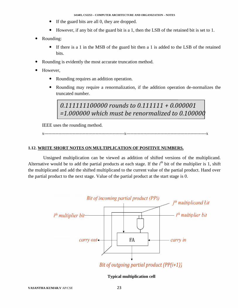
1.12. WRITE SHORT NOTES ON MULTIPLICATION OF POSITIVE NUMBERS.
Unsigned multiplication can be viewed as addition of shifted versions of the multiplicand.Alternative would be to add the partial products at each stage. If the ith bit of the multiplier is 1, shiftthe multiplicand and add the shifted multiplicand to the current value of the partial product. Hand overthe partial product to the next stage. Value of the partial product at the start stage is 0.
Typical multiplication cell
141403, CS2253 – COMPUTER ARCHITECTURE AND ORGANIZATION – NOTES
VASANTHA KUMAR.V AP/CSE 23
If the guard bits are all 0, they are dropped.
However, if any bit of the guard bit is a 1, then the LSB of the retained bit is set to 1.
Rounding:
If there is a 1 in the MSB of the guard bit then a 1 is added to the LSB of the retainedbits.
Rounding is evidently the most accurate truncation method.
However,
Rounding requires an addition operation.
Rounding may require a renormalization, if the addition operation de-normalizes thetruncated number.
IEEE uses the rounding method.
x--------------------------------------------------------x--------------------------------------------------------x
1.12. WRITE SHORT NOTES ON MULTIPLICATION OF POSITIVE NUMBERS.
Unsigned multiplication can be viewed as addition of shifted versions of the multiplicand.Alternative would be to add the partial products at each stage. If the ith bit of the multiplier is 1, shiftthe multiplicand and add the shifted multiplicand to the current value of the partial product. Hand overthe partial product to the next stage. Value of the partial product at the start stage is 0.
Typical multiplication cell
141403, CS2253 – COMPUTER ARCHITECTURE AND ORGANIZATION – NOTES
VASANTHA KUMAR.V AP/CSE 24
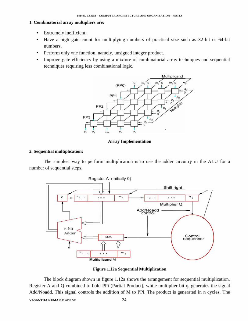
1. Combinatorial array multipliers are:
Extremely inefficient. Have a high gate count for multiplying numbers of practical size such as 32-bit or 64-bit
numbers. Perform only one function, namely, unsigned integer product. Improve gate efficiency by using a mixture of combinatorial array techniques and sequential
techniques requiring less combinational logic.
Array Implementation
2. Sequential multiplication:
The simplest way to perform multiplication is to use the adder circuitry in the ALU for anumber of sequential steps.
Figure 1.12a Sequential Multiplication
The block diagram shown in figure 1.12a shows the arrangement for sequential multiplication.Register A and Q combined to hold PPi (Partial Product), while multiplier bit qi generates the signalAdd/Noadd. This signal controls the addition of M to PPi. The product is generated in n cycles. The
141403, CS2253 – COMPUTER ARCHITECTURE AND ORGANIZATION – NOTES
VASANTHA KUMAR.V AP/CSE 24
1. Combinatorial array multipliers are:
Extremely inefficient. Have a high gate count for multiplying numbers of practical size such as 32-bit or 64-bit
numbers. Perform only one function, namely, unsigned integer product. Improve gate efficiency by using a mixture of combinatorial array techniques and sequential
techniques requiring less combinational logic.
Array Implementation
2. Sequential multiplication:
The simplest way to perform multiplication is to use the adder circuitry in the ALU for anumber of sequential steps.
Figure 1.12a Sequential Multiplication
The block diagram shown in figure 1.12a shows the arrangement for sequential multiplication.Register A and Q combined to hold PPi (Partial Product), while multiplier bit qi generates the signalAdd/Noadd. This signal controls the addition of M to PPi. The product is generated in n cycles. The
141403, CS2253 – COMPUTER ARCHITECTURE AND ORGANIZATION – NOTES
VASANTHA KUMAR.V AP/CSE 25
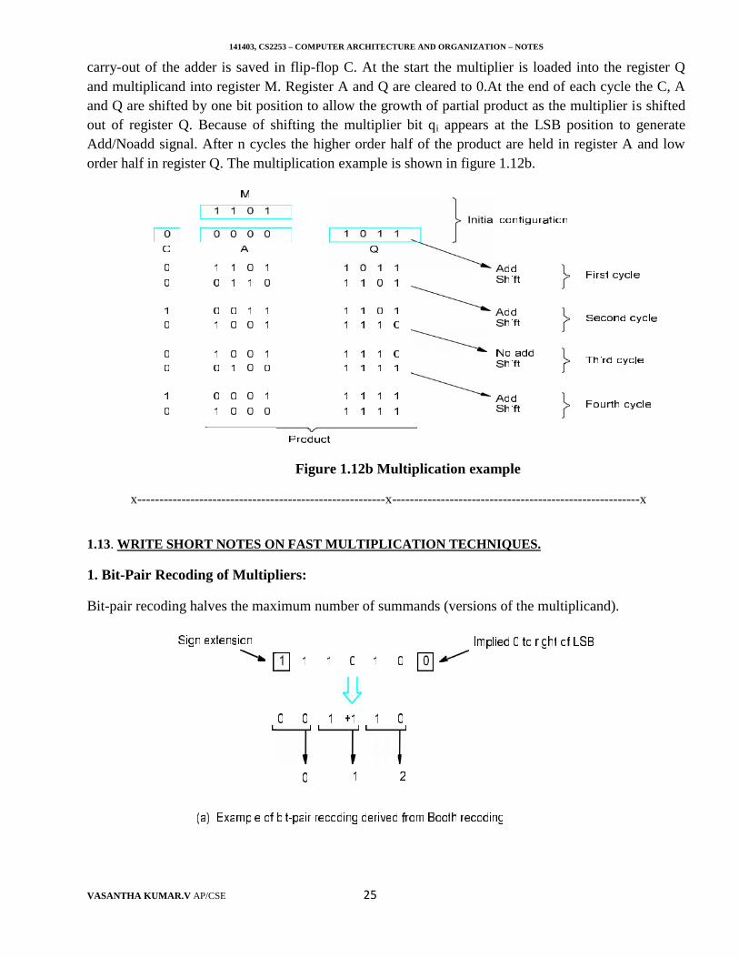
carry-out of the adder is saved in flip-flop C. At the start the multiplier is loaded into the register Qand multiplicand into register M. Register A and Q are cleared to 0.At the end of each cycle the C, Aand Q are shifted by one bit position to allow the growth of partial product as the multiplier is shiftedout of register Q. Because of shifting the multiplier bit qi appears at the LSB position to generateAdd/Noadd signal. After n cycles the higher order half of the product are held in register A and loworder half in register Q. The multiplication example is shown in figure 1.12b.
Figure 1.12b Multiplication example
x--------------------------------------------------------x--------------------------------------------------------x
1.13. WRITE SHORT NOTES ON FAST MULTIPLICATION TECHNIQUES.
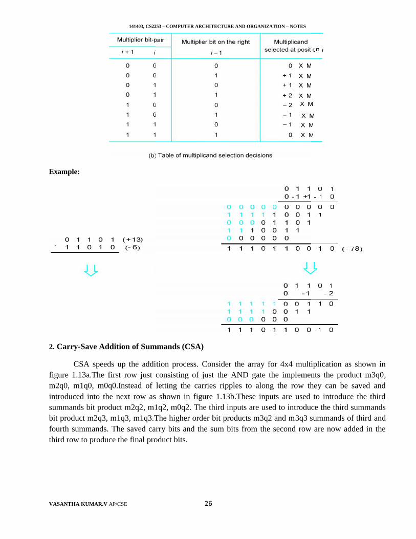
1. Bit-Pair Recoding of Multipliers:
Bit-pair recoding halves the maximum number of summands (versions of the multiplicand).
141403, CS2253 – COMPUTER ARCHITECTURE AND ORGANIZATION – NOTES
VASANTHA KUMAR.V AP/CSE 25
carry-out of the adder is saved in flip-flop C. At the start the multiplier is loaded into the register Qand multiplicand into register M. Register A and Q are cleared to 0.At the end of each cycle the C, Aand Q are shifted by one bit position to allow the growth of partial product as the multiplier is shiftedout of register Q. Because of shifting the multiplier bit qi appears at the LSB position to generateAdd/Noadd signal. After n cycles the higher order half of the product are held in register A and loworder half in register Q. The multiplication example is shown in figure 1.12b.
Figure 1.12b Multiplication example
x--------------------------------------------------------x--------------------------------------------------------x
1.13. WRITE SHORT NOTES ON FAST MULTIPLICATION TECHNIQUES.
1. Bit-Pair Recoding of Multipliers:
Bit-pair recoding halves the maximum number of summands (versions of the multiplicand).
141403, CS2253 – COMPUTER ARCHITECTURE AND ORGANIZATION – NOTES
VASANTHA KUMAR.V AP/CSE 26
Example:
2. Carry-Save Addition of Summands (CSA)
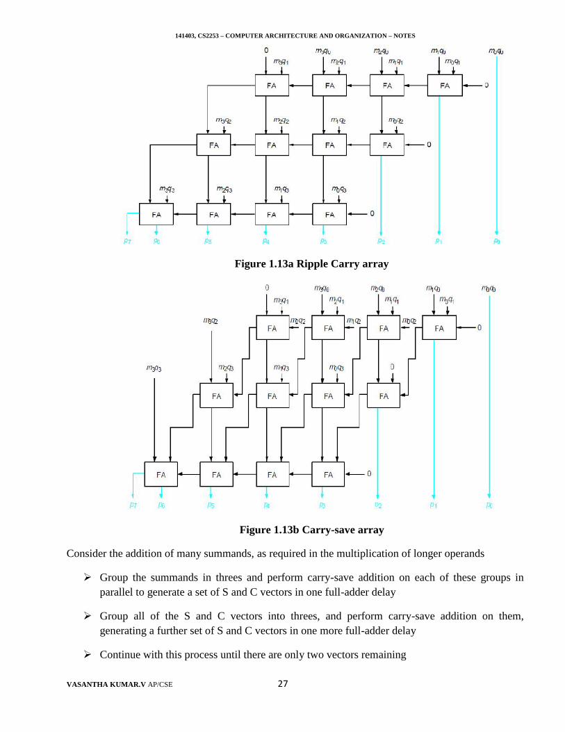
CSA speeds up the addition process. Consider the array for 4x4 multiplication as shown infigure 1.13a.The first row just consisting of just the AND gate the implements the product m3q0,m2q0, m1q0, m0q0.Instead of letting the carries ripples to along the row they can be saved andintroduced into the next row as shown in figure 1.13b.These inputs are used to introduce the thirdsummands bit product m2q2, m1q2, m0q2. The third inputs are used to introduce the third summandsbit product m2q3, m1q3, m1q3.The higher order bit products m3q2 and m3q3 summands of third andfourth summands. The saved carry bits and the sum bits from the second row are now added in thethird row to produce the final product bits.
141403, CS2253 – COMPUTER ARCHITECTURE AND ORGANIZATION – NOTES
VASANTHA KUMAR.V AP/CSE 26
Example:
2. Carry-Save Addition of Summands (CSA)
CSA speeds up the addition process. Consider the array for 4x4 multiplication as shown infigure 1.13a.The first row just consisting of just the AND gate the implements the product m3q0,m2q0, m1q0, m0q0.Instead of letting the carries ripples to along the row they can be saved andintroduced into the next row as shown in figure 1.13b.These inputs are used to introduce the thirdsummands bit product m2q2, m1q2, m0q2. The third inputs are used to introduce the third summandsbit product m2q3, m1q3, m1q3.The higher order bit products m3q2 and m3q3 summands of third andfourth summands. The saved carry bits and the sum bits from the second row are now added in thethird row to produce the final product bits.
141403, CS2253 – COMPUTER ARCHITECTURE AND ORGANIZATION – NOTES
VASANTHA KUMAR.V AP/CSE 27
Figure 1.13a Ripple Carry array
Figure 1.13b Carry-save array
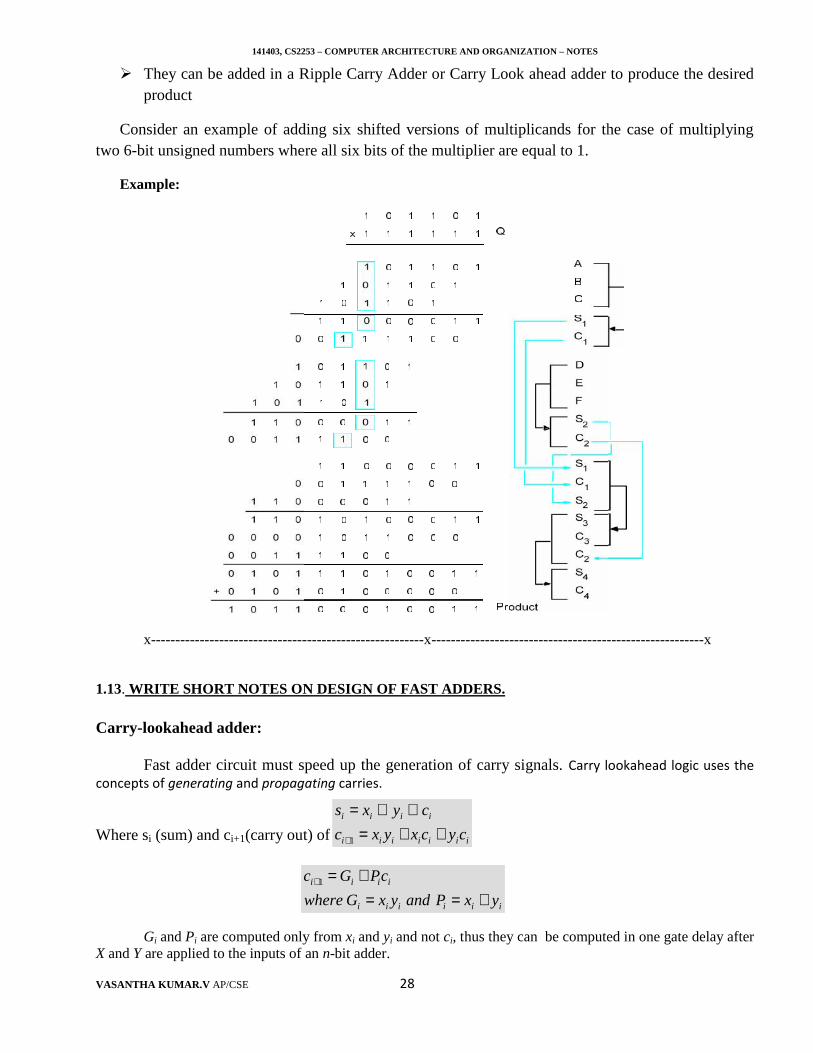
Consider the addition of many summands, as required in the multiplication of longer operands
Group the summands in threes and perform carry-save addition on each of these groups inparallel to generate a set of S and C vectors in one full-adder delay
Group all of the S and C vectors into threes, and perform carry-save addition on them,generating a further set of S and C vectors in one more full-adder delay
Continue with this process until there are only two vectors remaining
141403, CS2253 – COMPUTER ARCHITECTURE AND ORGANIZATION – NOTES
VASANTHA KUMAR.V AP/CSE 28
They can be added in a Ripple Carry Adder or Carry Look ahead adder to produce the desiredproduct
Consider an example of adding six shifted versions of multiplicands for the case of multiplyingtwo 6-bit unsigned numbers where all six bits of the multiplier are equal to 1.
Example:
x--------------------------------------------------------x--------------------------------------------------------x
1.13. WRITE SHORT NOTES ON DESIGN OF FAST ADDERS.
Carry-lookahead adder:
Fast adder circuit must speed up the generation of carry signals. Carry lookahead logic uses theconcepts of generating and propagating carries.
Where si (sum) and ci+1(carry out) of stage i.
Gi and Pi are computed only from xi and yi and not ci, thus they can be computed in one gate delay afterX and Y are applied to the inputs of an n-bit adder.
iiiiii
iiii
yxPandyxGwhere
cPGc
1
141403, CS2253 – COMPUTER ARCHITECTURE AND ORGANIZATION – NOTES
VASANTHA KUMAR.V AP/CSE 28
They can be added in a Ripple Carry Adder or Carry Look ahead adder to produce the desiredproduct
Consider an example of adding six shifted versions of multiplicands for the case of multiplyingtwo 6-bit unsigned numbers where all six bits of the multiplier are equal to 1.
Example:
x--------------------------------------------------------x--------------------------------------------------------x
1.13. WRITE SHORT NOTES ON DESIGN OF FAST ADDERS.
Carry-lookahead adder:
Fast adder circuit must speed up the generation of carry signals. Carry lookahead logic uses theconcepts of generating and propagating carries.
Where si (sum) and ci+1(carry out) of stage i.
Gi and Pi are computed only from xi and yi and not ci, thus they can be computed in one gate delay afterX and Y are applied to the inputs of an n-bit adder.
iiiiiii
iiii
cycxyxc
cyxs
1
iiiiii
iiii
yxPandyxGwhere
cPGc
1
141403, CS2253 – COMPUTER ARCHITECTURE AND ORGANIZATION – NOTES
VASANTHA KUMAR.V AP/CSE 28
They can be added in a Ripple Carry Adder or Carry Look ahead adder to produce the desiredproduct
Consider an example of adding six shifted versions of multiplicands for the case of multiplyingtwo 6-bit unsigned numbers where all six bits of the multiplier are equal to 1.
Example:
x--------------------------------------------------------x--------------------------------------------------------x
1.13. WRITE SHORT NOTES ON DESIGN OF FAST ADDERS.
Carry-lookahead adder:
Fast adder circuit must speed up the generation of carry signals. Carry lookahead logic uses theconcepts of generating and propagating carries.
Where si (sum) and ci+1(carry out) of stage i.
Gi and Pi are computed only from xi and yi and not ci, thus they can be computed in one gate delay afterX and Y are applied to the inputs of an n-bit adder.
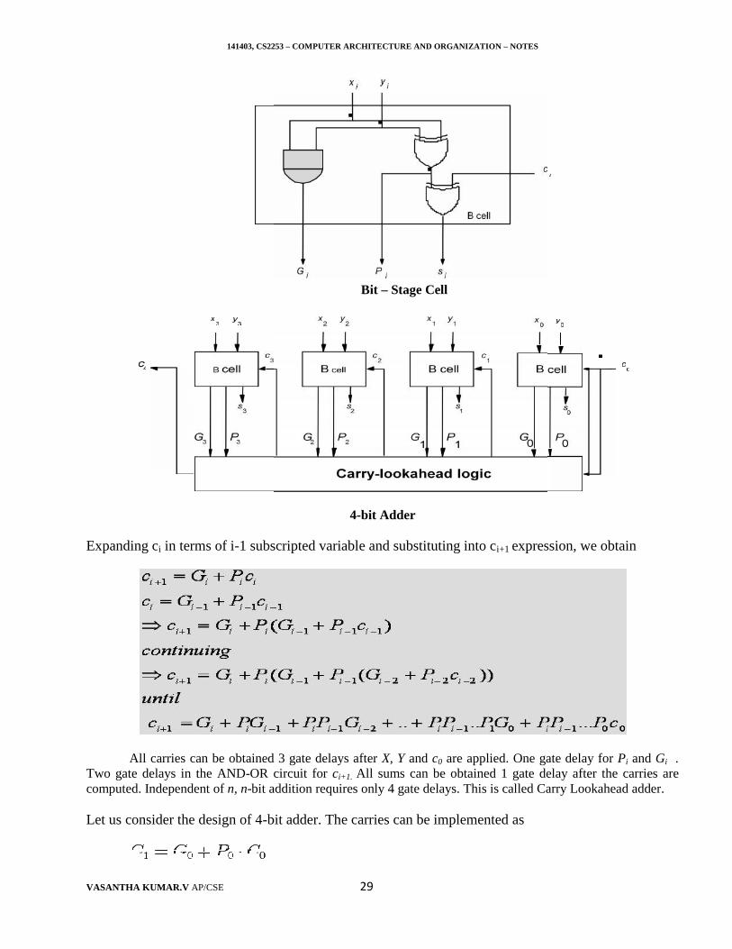
141403, CS2253 – COMPUTER ARCHITECTURE AND ORGANIZATION – NOTES
VASANTHA KUMAR.V AP/CSE 29
Bit – Stage Cell
4-bit Adder
Expanding ci in terms of i-1 subscripted variable and substituting into ci+1 expression, we obtain
All carries can be obtained 3 gate delays after X, Y and c0 are applied. One gate delay for Pi and Gi .Two gate delays in the AND-OR circuit for ci+1. All sums can be obtained 1 gate delay after the carries arecomputed. Independent of n, n-bit addition requires only 4 gate delays. This is called Carry Lookahead adder.
Let us consider the design of 4-bit adder. The carries can be implemented as
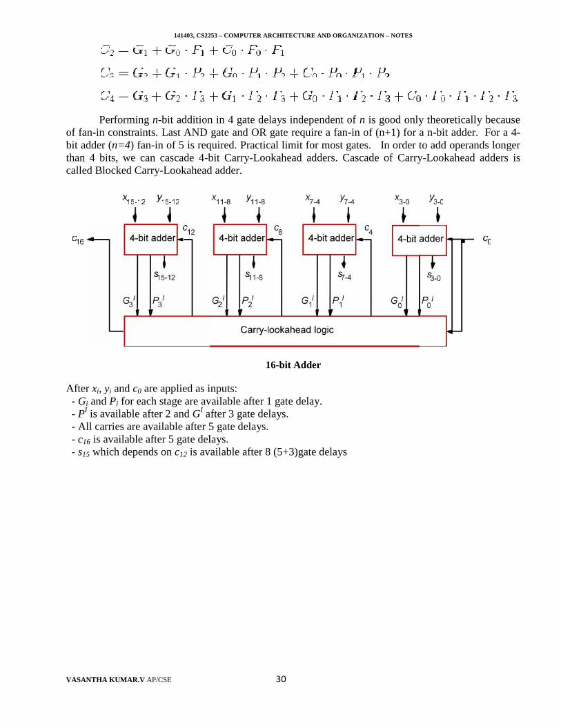
141403, CS2253 – COMPUTER ARCHITECTURE AND ORGANIZATION – NOTES
VASANTHA KUMAR.V AP/CSE 30
Performing n-bit addition in 4 gate delays independent of n is good only theoretically becauseof fan-in constraints. Last AND gate and OR gate require a fan-in of (n+1) for a n-bit adder. For a 4-bit adder (n=4) fan-in of 5 is required. Practical limit for most gates. In order to add operands longerthan 4 bits, we can cascade 4-bit Carry-Lookahead adders. Cascade of Carry-Lookahead adders iscalled Blocked Carry-Lookahead adder.
16-bit Adder
After xi, yi and c0 are applied as inputs:- Gi and Pi for each stage are available after 1 gate delay.- PI is available after 2 and GI after 3 gate delays.- All carries are available after 5 gate delays.- c16 is available after 5 gate delays.- s15 which depends on c12 is available after 8 (5+3)gate delays
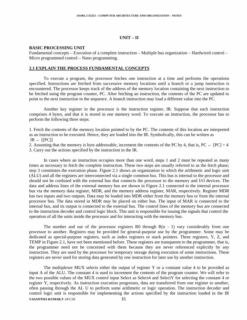
141403, CS2253 – COMPUTER ARCHITECTURE AND ORGANIZATION – NOTES
VASANTHA KUMAR.V AP/CSE 31
UNIT – II
BASIC PROCESSING UNITFundamental concepts – Execution of a complete instruction – Multiple bus organization – Hardwired control –Micro programmed control – Nano programming.
2.1 EXPLAIN THE PROCESS FUNDAMENTAL CONCEPTS
To execute a program, the processor fetches one instruction at a time and performs the operationsspecified. Instructions are fetched from successive memory locations until a branch or a jump instruction isencountered. The processor keeps track of the address of the memory location containing the next instruction tobe fetched using the program counter, PC. After fetching an instruction, the contents of the PC are updated topoint to the next instruction in the sequence. A branch instruction may load a different value into the PC.
Another key register in the processor is the instruction register, IR. Suppose that each instructioncomprises 4 bytes, and that it is stored in one memory word. To execute an instruction, the processor has toperform the following three steps:
1. Fetch the contents of the memory location pointed to by the PC. The contents of this location are interpretedas an instruction to be executed. Hence, they are loaded into the IR. Symbolically, this can be written asIR ← [[PC]]
2. Assuming that the memory is byte addressable, increment the contents of the PC by 4, that is, PC ← [PC] + 43. Carry out the actions specified by the instruction in the IR.
In cases where an instruction occupies more than one word, steps 1 and 2 must be repeated as manytimes as necessary to fetch the complete instruction. These two steps are usually referred to as the fetch phase;step 3 constitutes the execution phase. Figure 2.1 shows an organization in which the arithmetic and logic unit(ALU) and all the registers are interconnected via a single common bus. This bus is internal to the processor andshould not be confused with the external bus that connects the processor to the memory and I/O devices. Thedata and address lines of the external memory bus are shown in Figure 2.1 connected to the internal processorbus via the memory data register, MDR, and the memory address register, MAR, respectively. Register MDRhas two inputs and two outputs. Data may be loaded into MDR either from the memory bus or from the internalprocessor bus. The data stored in MDR may be placed on either bus. The input of MAR is connected to theinternal bus, and its output is connected to the external bus. The control lines of the memory bus are connectedto the instruction decoder and control logic block. This unit is responsible for issuing the signals that control theoperation of all the units inside the processor and for interacting with the memory bus.
The number and use of the processor registers R0 through R(n - 1) vary considerably from oneprocessor to another. Registers may be provided for general-purpose use by the programmer. Some may bededicated as special-purpose registers, such as index registers or stack pointers. Three registers, Y, Z, andTEMP in Figure 2.1, have not been mentioned before. These registers are transparent to the programmer, that is,the programmer need not be concerned with them because they are never referenced explicitly by anyinstruction. They are used by the processor for temporary storage during execution of some instructions. Theseregisters are never used for storing data generated by one instruction for later use by another instruction.
The multiplexer MUX selects either the output of register Y or a constant value 4 to be provided asinput A of the ALU. The constant 4 is used to increment the contents of the program counter. We will refer tothe two possible values of the MUX control input Select as Select4 and SelectY for selecting the constant 4 orregister Y, respectively. As instruction execution progresses, data are transferred from one register to another,often passing through the AL U to perform some arithmetic or logic operation. The instruction decoder andcontrol logic unit is responsible for implementing the actions specified by the instruction loaded in the IR
141403, CS2253 – COMPUTER ARCHITECTURE AND ORGANIZATION – NOTES
VASANTHA KUMAR.V AP/CSE 32
register. The decoder generates the control signals needed to select the registers involved and direct the transferof data. The registers, the ALU, and the interconnecting bus are collectively referred to as the datapath.
With few exceptions, an instruction can be executed by performing one or more of the following operations insome specified sequence:· Transfer a word of data from one processor register to another or to the ALU· Perform arithmetic or a logic operation and store the result in a processor register· Fetch the contents of a given memory location and load them into a processor register· Store a word of data from a processor register into a given memory location
Register Transfers
Instruction execution involves a sequence of steps in which data are transferred from one register toanother. For each register, two control signals are used to place the contents of that register on the bus or toload the data on the bus into the register. This is represented symbolically in Figure 2.2. The input andoutput of register Ri are connected to the bus via switches controlled by the signals Riin and Ri outrespectively. When Riin is set to 1, the data on the bus are loaded into Ri. Similarly, when Riout is set to 1,the contents of register Ri are placed on the bus. While Riout is equal to 0, the bus can be used fortransferring data from other registers. Suppose that we wish to transfer the contents of register Rl toregister R4. This can be accomplished as follows:
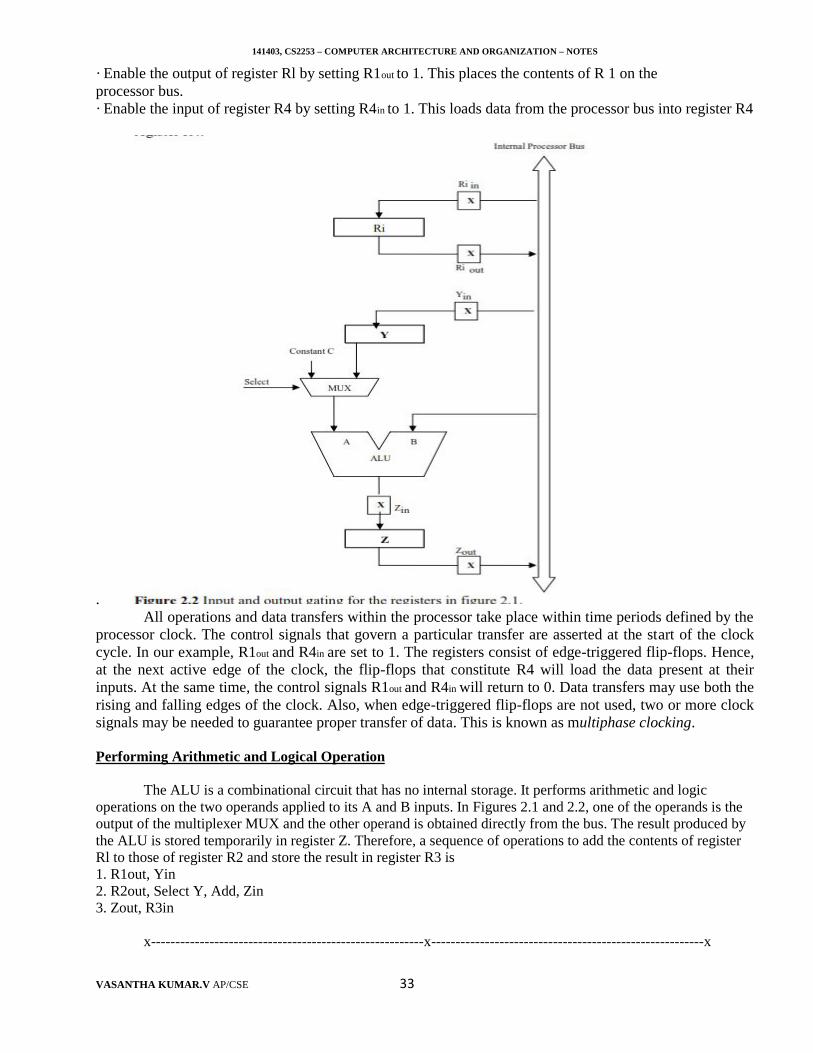
141403, CS2253 – COMPUTER ARCHITECTURE AND ORGANIZATION – NOTES
VASANTHA KUMAR.V AP/CSE 33
· Enable the output of register Rl by setting R1out to 1. This places the contents of R 1 on theprocessor bus.· Enable the input of register R4 by setting R4in to 1. This loads data from the processor bus into register R4
.All operations and data transfers within the processor take place within time periods defined by the
processor clock. The control signals that govern a particular transfer are asserted at the start of the clockcycle. In our example, R1out and R4in are set to 1. The registers consist of edge-triggered flip-flops. Hence,at the next active edge of the clock, the flip-flops that constitute R4 will load the data present at theirinputs. At the same time, the control signals R1out and R4in will return to 0. Data transfers may use both therising and falling edges of the clock. Also, when edge-triggered flip-flops are not used, two or more clocksignals may be needed to guarantee proper transfer of data. This is known as multiphase clocking.
Performing Arithmetic and Logical Operation
The ALU is a combinational circuit that has no internal storage. It performs arithmetic and logicoperations on the two operands applied to its A and B inputs. In Figures 2.1 and 2.2, one of the operands is theoutput of the multiplexer MUX and the other operand is obtained directly from the bus. The result produced bythe ALU is stored temporarily in register Z. Therefore, a sequence of operations to add the contents of registerRl to those of register R2 and store the result in register R3 is1. R1out, Yin2. R2out, Select Y, Add, Zin3. Zout, R3in
x--------------------------------------------------------x--------------------------------------------------------x
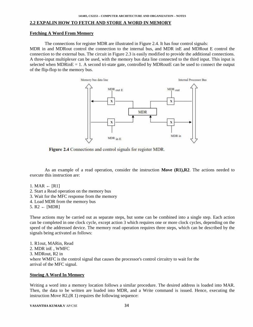
141403, CS2253 – COMPUTER ARCHITECTURE AND ORGANIZATION – NOTES
VASANTHA KUMAR.V AP/CSE 34
2.2 EXPALIN HOW TO FETCH AND STORE A WORD IN MEMORY
Fetching A Word From Memory
The connections for register MDR are illustrated in Figure 2.4. It has four control signals:MDR in and MDRout control the connection to the internal bus, and MDR inE and MDRout E control theconnection to the external bus. The circuit in Figure 2.3 is easily modified to provide the additional connections.A three-input multiplexer can be used, with the memory bus data line connected to the third input. This input isselected when MDRinE = 1. A second tri-state gate, controlled by MDRoutE can be used to connect the outputof the flip-flop to the memory bus.
As an example of a read operation, consider the instruction Move (R1),R2. The actions needed toexecute this instruction are:
1. MAR [R1]2. Start a Read operation on the memory bus3. Wait for the MFC response from the memory4. Load MDR from the memory bus5. R2 ← [MDR]
These actions may be carried out as separate steps, but some can be combined into a single step. Each actioncan be completed in one clock cycle, except action 3 which requires one or more clock cycles, depending on thespeed of the addressed device. The memory read operation requires three steps, which can be described by thesignals being activated as follows:
1. R1out, MARin, Read2. MDR inE , WMFC3. MDRout, R2 inwhere WMFC is the control signal that causes the processor's control circuitry to wait for thearrival of the MFC signal.
Storing A Word In Memory
Writing a word into a memory location follows a similar procedure. The desired address is loaded into MAR.Then, the data to be written are loaded into MDR, and a Write command is issued. Hence, executing theinstruction Move R2,(R 1) requires the following sequence:
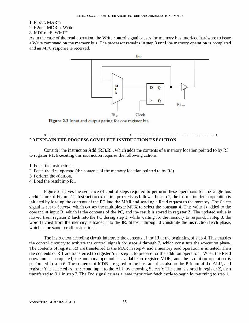
141403, CS2253 – COMPUTER ARCHITECTURE AND ORGANIZATION – NOTES
VASANTHA KUMAR.V AP/CSE 35
1. R1out, MARin2. R2out, MDRin, Write3. MDRoutE, WMFCAs in the case of the read operation, the Write control signal causes the memory bus interface hardware to issuea Write command on the memory bus. The processor remains in step 3 until the memory operation is completedand an MFC response is received.
x--------------------------------------------------------x--------------------------------------------------------x2.3 EXPLAIN THE PROCESS COMPLETE INSTRUCTION EXECUTION
Consider the instruction Add (R3),Rl , which adds the contents of a memory location pointed to by R3to register R1. Executing this instruction requires the following actions:
1. Fetch the instruction.2. Fetch the first operand (the contents of the memory location pointed to by R3).3. Perform the addition.4. Load the result into R1.
Figure 2.5 gives the sequence of control steps required to perform these operations for the single busarchitecture of Figure 2.1. Instruction execution proceeds as follows. In step 1, the instruction fetch operation isinitiated by loading the contents of the PC into the MAR and sending a Read request to the memory. The Selectsignal is set to Select4, which causes the multiplexer MUX to select the constant 4. This value is added to theoperand at input B, which is the contents of the PC, and the result is stored in register Z. The updated value ismoved from register Z back into the PC during step 2, while waiting for the memory to respond. In step 3, theword fetched from the memory is loaded into the IR. Steps 1 through 3 constitute the instruction fetch phase,which is the same for all instructions.
The instruction decoding circuit interprets the contents of the IR at the beginning of step 4. This enablesthe control circuitry to activate the control signals for steps 4 through 7, which constitute the execution phase.The contents of register R3 are transferred to the MAR in step 4, and a memory read operation is initiated. Thenthe contents of R 1 are transferred to register Y in step 5, to prepare for the addition operation. When the Readoperation is completed, the memory operand is available in register MDR, and the addition operation isperformed in step 6. The contents of MDR are gated to the bus, and thus also to the B input of the ALU, andregister Y is selected as the second input to the ALU by choosing Select Y The sum is stored in register Z, thentransferred to R 1 in step 7. The End signal causes a new instruction fetch cycle to begin by returning to step 1.
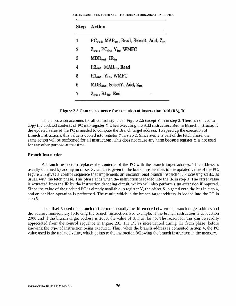
141403, CS2253 – COMPUTER ARCHITECTURE AND ORGANIZATION – NOTES
VASANTHA KUMAR.V AP/CSE 36
Figure 2.5 Control sequence for execution of instruction Add (R3), Rl.
This discussion accounts for all control signals in Figure 2.5 except Y in in step 2. There is no need tocopy the updated contents of PC into register Y when executing the Add instruction. But, in Branch instructionsthe updated value of the PC is needed to compute the Branch target address. To speed up the execution ofBranch instructions, this value is copied into register Y in step 2. Since step 2 is part of the fetch phase, thesame action will be performed for all instructions. This does not cause any harm because register Y is not usedfor any other purpose at that time.
Branch Instruction
A branch instruction replaces the contents of the PC with the branch target address. This address isusually obtained by adding an offset X, which is given in the branch instruction, to the updated value of the PC.Figure 2.6 gives a control sequence that implements an unconditional branch instruction. Processing starts, asusual, with the fetch phase. This phase ends when the instruction is loaded into the IR in step 3. The offset valueis extracted from the IR by the instruction decoding circuit, which will also perform sign extension if required.Since the value of the updated PC is already available in register Y, the offset X is gated onto the bus in step 4,and an addition operation is performed. The result, which is the branch target address, is loaded into the PC instep 5.
The offset X used in a branch instruction is usually the difference between the branch target address andthe address immediately following the branch instruction. For example, if the branch instruction is at location2000 and if the branch target address is 2050, the value of X must be 46. The reason for this can be readilyappreciated from the control sequence in Figure 2.6. The PC is incremented during the fetch phase, beforeknowing the type of instruction being executed. Thus, when the branch address is computed in step 4, the PCvalue used is the updated value, which points to the instruction following the branch instruction in the memory.
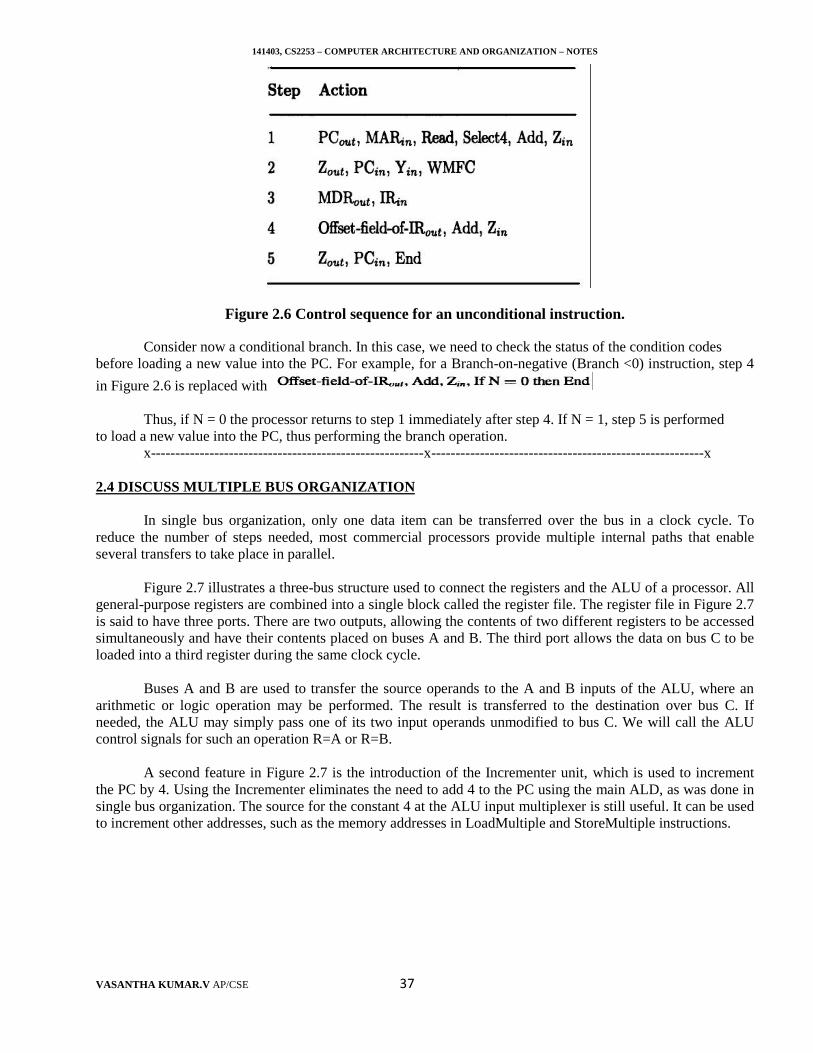
141403, CS2253 – COMPUTER ARCHITECTURE AND ORGANIZATION – NOTES
VASANTHA KUMAR.V AP/CSE 37
Figure 2.6 Control sequence for an unconditional instruction.
Consider now a conditional branch. In this case, we need to check the status of the condition codesbefore loading a new value into the PC. For example, for a Branch-on-negative (Branch <0) instruction, step 4
in Figure 2.6 is replaced with
Thus, if N = 0 the processor returns to step 1 immediately after step 4. If N = 1, step 5 is performedto load a new value into the PC, thus performing the branch operation.
x--------------------------------------------------------x--------------------------------------------------------x
2.4 DISCUSS MULTIPLE BUS ORGANIZATION
In single bus organization, only one data item can be transferred over the bus in a clock cycle. Toreduce the number of steps needed, most commercial processors provide multiple internal paths that enableseveral transfers to take place in parallel.
Figure 2.7 illustrates a three-bus structure used to connect the registers and the ALU of a processor. Allgeneral-purpose registers are combined into a single block called the register file. The register file in Figure 2.7is said to have three ports. There are two outputs, allowing the contents of two different registers to be accessedsimultaneously and have their contents placed on buses A and B. The third port allows the data on bus C to beloaded into a third register during the same clock cycle.
Buses A and B are used to transfer the source operands to the A and B inputs of the ALU, where anarithmetic or logic operation may be performed. The result is transferred to the destination over bus C. Ifneeded, the ALU may simply pass one of its two input operands unmodified to bus C. We will call the ALUcontrol signals for such an operation R=A or R=B.
A second feature in Figure 2.7 is the introduction of the Incrementer unit, which is used to incrementthe PC by 4. Using the Incrementer eliminates the need to add 4 to the PC using the main ALD, as was done insingle bus organization. The source for the constant 4 at the ALU input multiplexer is still useful. It can be usedto increment other addresses, such as the memory addresses in LoadMultiple and StoreMultiple instructions.
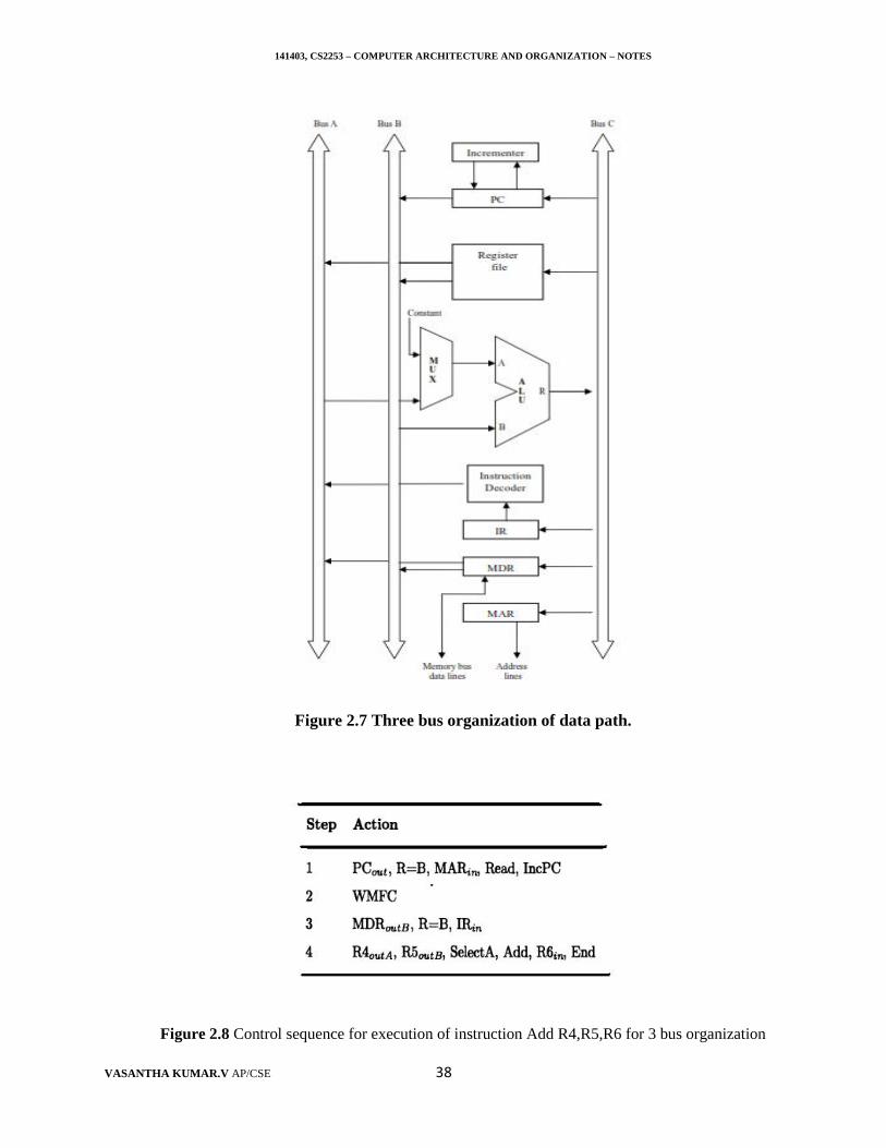
141403, CS2253 – COMPUTER ARCHITECTURE AND ORGANIZATION – NOTES
VASANTHA KUMAR.V AP/CSE 38
Figure 2.7 Three bus organization of data path.
Figure 2.8 Control sequence for execution of instruction Add R4,R5,R6 for 3 bus organization
141403, CS2253 – COMPUTER ARCHITECTURE AND ORGANIZATION – NOTES
VASANTHA KUMAR.V AP/CSE 38
Figure 2.7 Three bus organization of data path.
Figure 2.8 Control sequence for execution of instruction Add R4,R5,R6 for 3 bus organization
141403, CS2253 – COMPUTER ARCHITECTURE AND ORGANIZATION – NOTES
VASANTHA KUMAR.V AP/CSE 38
Figure 2.7 Three bus organization of data path.
Figure 2.8 Control sequence for execution of instruction Add R4,R5,R6 for 3 bus organization
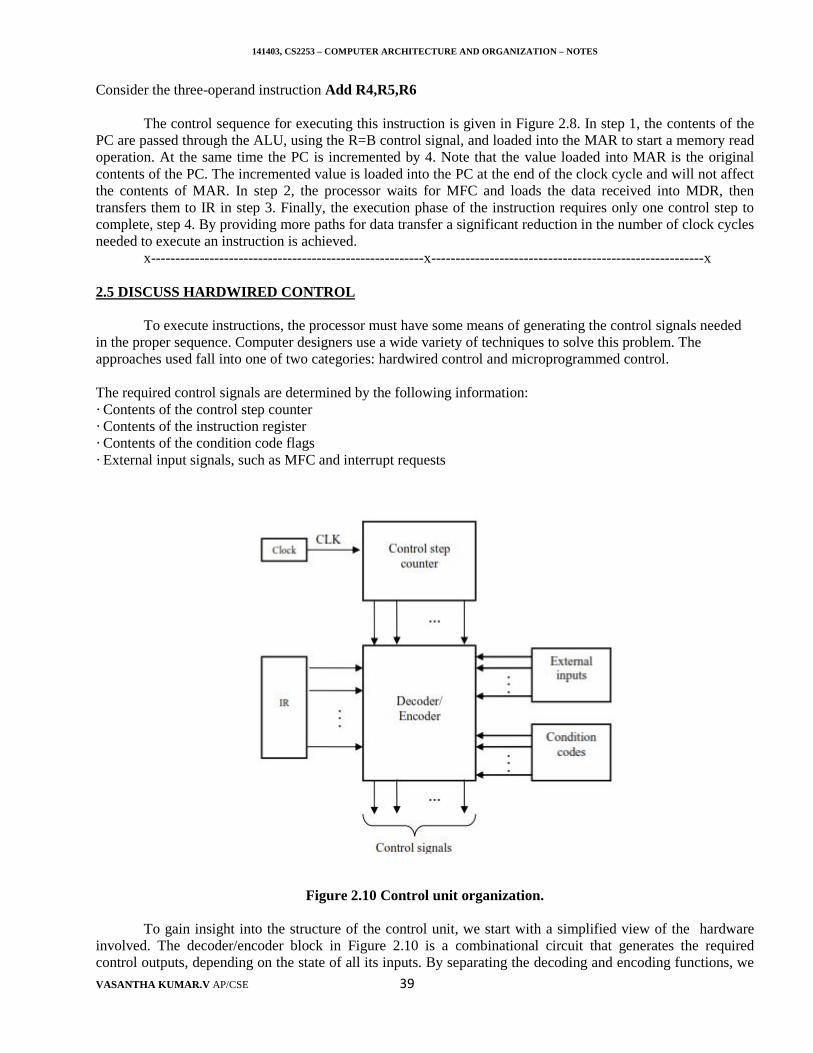
141403, CS2253 – COMPUTER ARCHITECTURE AND ORGANIZATION – NOTES
VASANTHA KUMAR.V AP/CSE 39
Consider the three-operand instruction Add R4,R5,R6
The control sequence for executing this instruction is given in Figure 2.8. In step 1, the contents of thePC are passed through the ALU, using the R=B control signal, and loaded into the MAR to start a memory readoperation. At the same time the PC is incremented by 4. Note that the value loaded into MAR is the originalcontents of the PC. The incremented value is loaded into the PC at the end of the clock cycle and will not affectthe contents of MAR. In step 2, the processor waits for MFC and loads the data received into MDR, thentransfers them to IR in step 3. Finally, the execution phase of the instruction requires only one control step tocomplete, step 4. By providing more paths for data transfer a significant reduction in the number of clock cyclesneeded to execute an instruction is achieved.
x--------------------------------------------------------x--------------------------------------------------------x
2.5 DISCUSS HARDWIRED CONTROL
To execute instructions, the processor must have some means of generating the control signals neededin the proper sequence. Computer designers use a wide variety of techniques to solve this problem. Theapproaches used fall into one of two categories: hardwired control and microprogrammed control.
The required control signals are determined by the following information:· Contents of the control step counter· Contents of the instruction register· Contents of the condition code flags· External input signals, such as MFC and interrupt requests
Figure 2.10 Control unit organization.
To gain insight into the structure of the control unit, we start with a simplified view of the hardwareinvolved. The decoder/encoder block in Figure 2.10 is a combinational circuit that generates the requiredcontrol outputs, depending on the state of all its inputs. By separating the decoding and encoding functions, we
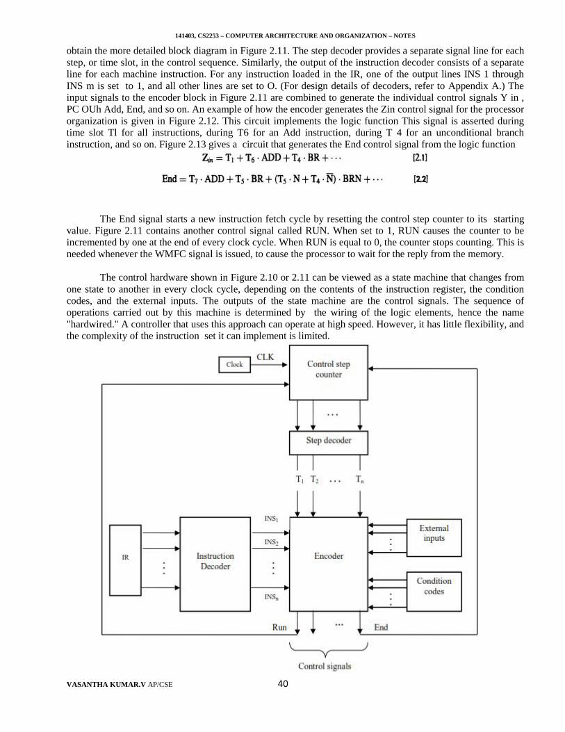
141403, CS2253 – COMPUTER ARCHITECTURE AND ORGANIZATION – NOTES
VASANTHA KUMAR.V AP/CSE 40
obtain the more detailed block diagram in Figure 2.11. The step decoder provides a separate signal line for eachstep, or time slot, in the control sequence. Similarly, the output of the instruction decoder consists of a separateline for each machine instruction. For any instruction loaded in the IR, one of the output lines INS 1 throughINS m is set to 1, and all other lines are set to O. (For design details of decoders, refer to Appendix A.) Theinput signals to the encoder block in Figure 2.11 are combined to generate the individual control signals Y in ,PC OUh Add, End, and so on. An example of how the encoder generates the Zin control signal for the processororganization is given in Figure 2.12. This circuit implements the logic function This signal is asserted duringtime slot Tl for all instructions, during T6 for an Add instruction, during T 4 for an unconditional branchinstruction, and so on. Figure 2.13 gives a circuit that generates the End control signal from the logic function
The End signal starts a new instruction fetch cycle by resetting the control step counter to its startingvalue. Figure 2.11 contains another control signal called RUN. When set to 1, RUN causes the counter to beincremented by one at the end of every clock cycle. When RUN is equal to 0, the counter stops counting. This isneeded whenever the WMFC signal is issued, to cause the processor to wait for the reply from the memory.
The control hardware shown in Figure 2.10 or 2.11 can be viewed as a state machine that changes fromone state to another in every clock cycle, depending on the contents of the instruction register, the conditioncodes, and the external inputs. The outputs of the state machine are the control signals. The sequence ofoperations carried out by this machine is determined by the wiring of the logic elements, hence the name"hardwired." A controller that uses this approach can operate at high speed. However, it has little flexibility, andthe complexity of the instruction set it can implement is limited.
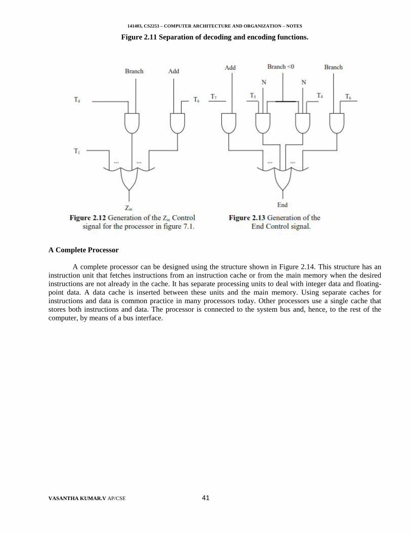
141403, CS2253 – COMPUTER ARCHITECTURE AND ORGANIZATION – NOTES
VASANTHA KUMAR.V AP/CSE 41
Figure 2.11 Separation of decoding and encoding functions.
A Complete Processor
A complete processor can be designed using the structure shown in Figure 2.14. This structure has aninstruction unit that fetches instructions from an instruction cache or from the main memory when the desiredinstructions are not already in the cache. It has separate processing units to deal with integer data and floating-point data. A data cache is inserted between these units and the main memory. Using separate caches forinstructions and data is common practice in many processors today. Other processors use a single cache thatstores both instructions and data. The processor is connected to the system bus and, hence, to the rest of thecomputer, by means of a bus interface.
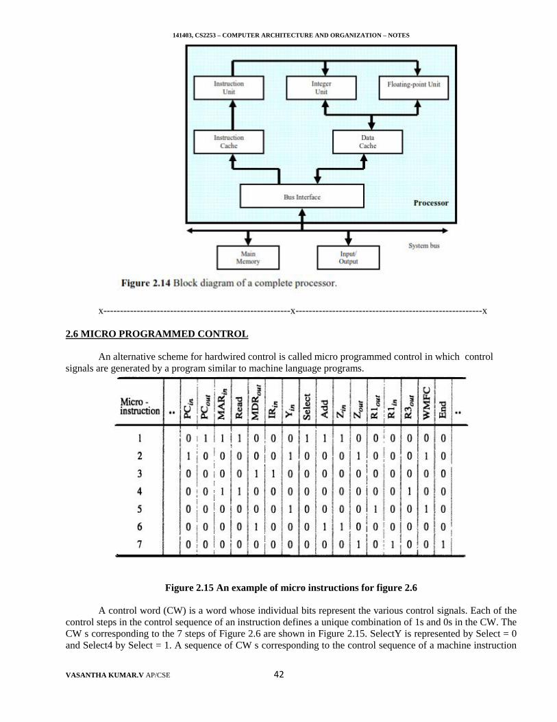
141403, CS2253 – COMPUTER ARCHITECTURE AND ORGANIZATION – NOTES
VASANTHA KUMAR.V AP/CSE 42
x--------------------------------------------------------x--------------------------------------------------------x
2.6 MICRO PROGRAMMED CONTROL
An alternative scheme for hardwired control is called micro programmed control in which controlsignals are generated by a program similar to machine language programs.
Figure 2.15 An example of micro instructions for figure 2.6
A control word (CW) is a word whose individual bits represent the various control signals. Each of thecontrol steps in the control sequence of an instruction defines a unique combination of 1s and 0s in the CW. TheCW s corresponding to the 7 steps of Figure 2.6 are shown in Figure 2.15. SelectY is represented by Select = 0and Select4 by Select = 1. A sequence of CW s corresponding to the control sequence of a machine instruction
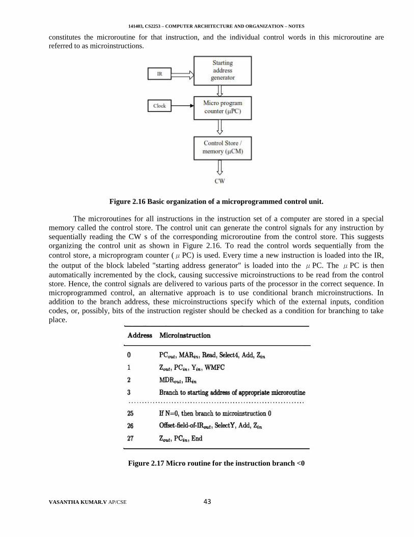
141403, CS2253 – COMPUTER ARCHITECTURE AND ORGANIZATION – NOTES
VASANTHA KUMAR.V AP/CSE 43
constitutes the microroutine for that instruction, and the individual control words in this microroutine arereferred to as microinstructions.
Figure 2.16 Basic organization of a microprogrammed control unit.
The microroutines for all instructions in the instruction set of a computer are stored in a specialmemory called the control store. The control unit can generate the control signals for any instruction bysequentially reading the CW s of the corresponding microroutine from the control store. This suggestsorganizing the control unit as shown in Figure 2.16. To read the control words sequentially from thecontrol store, a microprogram counter (μPC) is used. Every time a new instruction is loaded into the IR,the output of the block labeled "starting address generator" is loaded into the μPC. The μPC is thenautomatically incremented by the clock, causing successive microinstructions to be read from the controlstore. Hence, the control signals are delivered to various parts of the processor in the correct sequence. Inmicroprogrammed control, an alternative approach is to use conditional branch microinstructions. Inaddition to the branch address, these microinstructions specify which of the external inputs, conditioncodes, or, possibly, bits of the instruction register should be checked as a condition for branching to takeplace.
Figure 2.17 Micro routine for the instruction branch <0
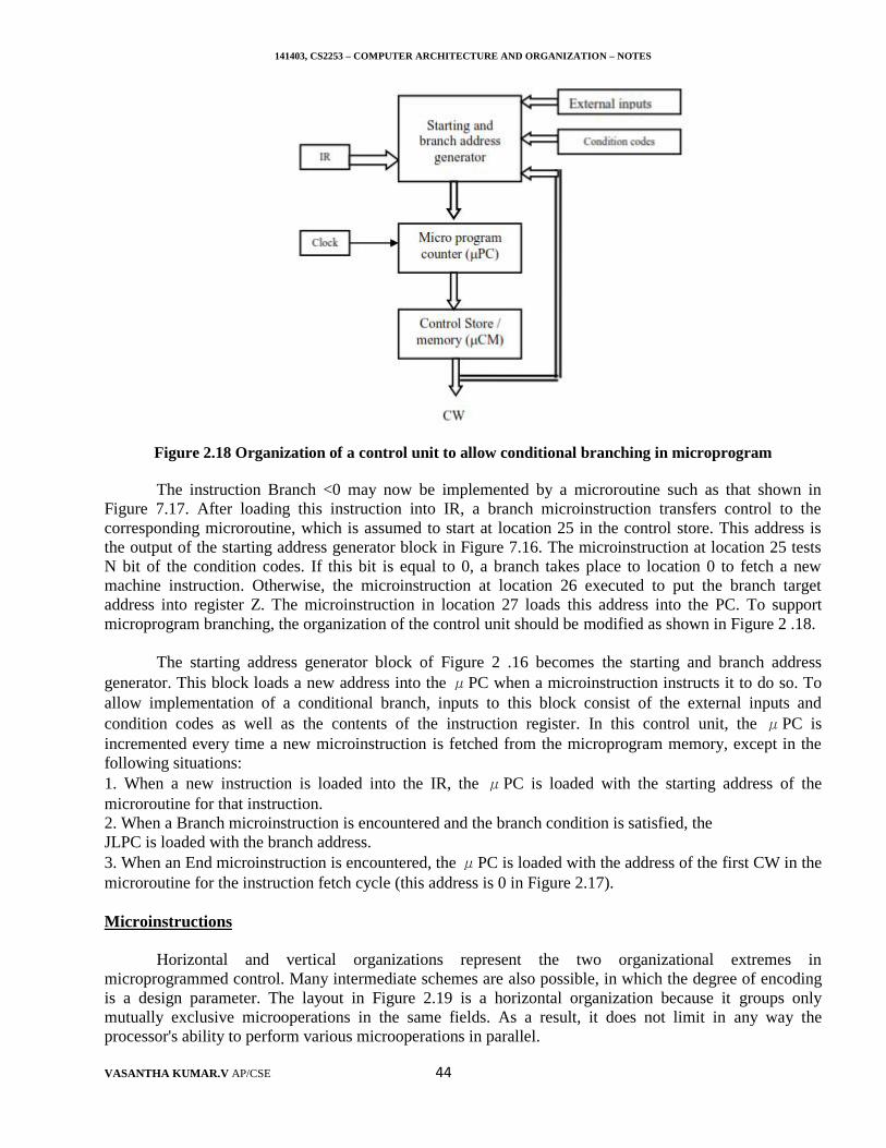
141403, CS2253 – COMPUTER ARCHITECTURE AND ORGANIZATION – NOTES
VASANTHA KUMAR.V AP/CSE 44
Figure 2.18 Organization of a control unit to allow conditional branching in microprogram
The instruction Branch <0 may now be implemented by a microroutine such as that shown inFigure 7.17. After loading this instruction into IR, a branch microinstruction transfers control to thecorresponding microroutine, which is assumed to start at location 25 in the control store. This address isthe output of the starting address generator block in Figure 7.16. The microinstruction at location 25 testsN bit of the condition codes. If this bit is equal to 0, a branch takes place to location 0 to fetch a newmachine instruction. Otherwise, the microinstruction at location 26 executed to put the branch targetaddress into register Z. The microinstruction in location 27 loads this address into the PC. To supportmicroprogram branching, the organization of the control unit should be modified as shown in Figure 2 .18.
The starting address generator block of Figure 2 .16 becomes the starting and branch addressgenerator. This block loads a new address into the μPC when a microinstruction instructs it to do so. Toallow implementation of a conditional branch, inputs to this block consist of the external inputs andcondition codes as well as the contents of the instruction register. In this control unit, the μPC isincremented every time a new microinstruction is fetched from the microprogram memory, except in thefollowing situations:1. When a new instruction is loaded into the IR, the μPC is loaded with the starting address of themicroroutine for that instruction.2. When a Branch microinstruction is encountered and the branch condition is satisfied, theJLPC is loaded with the branch address.3. When an End microinstruction is encountered, theμPC is loaded with the address of the first CW in themicroroutine for the instruction fetch cycle (this address is 0 in Figure 2.17).
Microinstructions
Horizontal and vertical organizations represent the two organizational extremes inmicroprogrammed control. Many intermediate schemes are also possible, in which the degree of encodingis a design parameter. The layout in Figure 2.19 is a horizontal organization because it groups onlymutually exclusive microoperations in the same fields. As a result, it does not limit in any way theprocessor's ability to perform various microoperations in parallel.
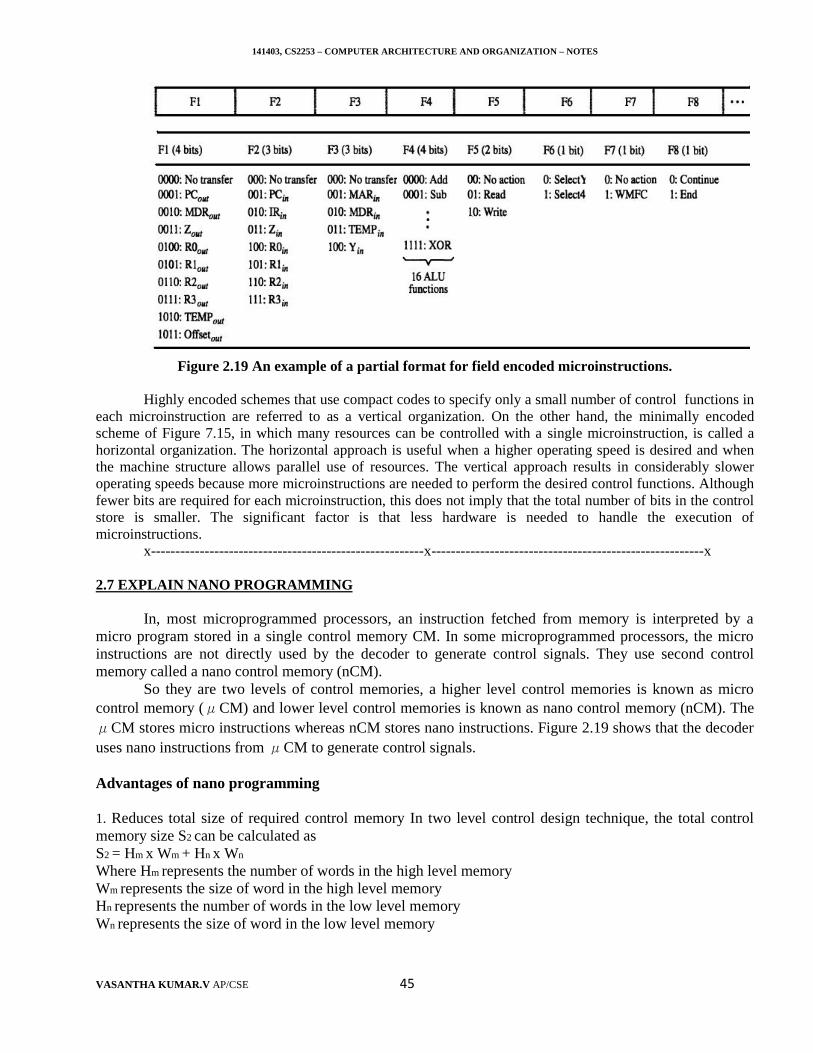
141403, CS2253 – COMPUTER ARCHITECTURE AND ORGANIZATION – NOTES
VASANTHA KUMAR.V AP/CSE 45
Figure 2.19 An example of a partial format for field encoded microinstructions.
Highly encoded schemes that use compact codes to specify only a small number of control functions ineach microinstruction are referred to as a vertical organization. On the other hand, the minimally encodedscheme of Figure 7.15, in which many resources can be controlled with a single microinstruction, is called ahorizontal organization. The horizontal approach is useful when a higher operating speed is desired and whenthe machine structure allows parallel use of resources. The vertical approach results in considerably sloweroperating speeds because more microinstructions are needed to perform the desired control functions. Althoughfewer bits are required for each microinstruction, this does not imply that the total number of bits in the controlstore is smaller. The significant factor is that less hardware is needed to handle the execution ofmicroinstructions.
x--------------------------------------------------------x--------------------------------------------------------x
2.7 EXPLAIN NANO PROGRAMMING
In, most microprogrammed processors, an instruction fetched from memory is interpreted by amicro program stored in a single control memory CM. In some microprogrammed processors, the microinstructions are not directly used by the decoder to generate control signals. They use second controlmemory called a nano control memory (nCM).
So they are two levels of control memories, a higher level control memories is known as microcontrol memory (μCM) and lower level control memories is known as nano control memory (nCM). TheμCM stores micro instructions whereas nCM stores nano instructions. Figure 2.19 shows that the decoderuses nano instructions fromμCM to generate control signals.
Advantages of nano programming
1. Reduces total size of required control memory In two level control design technique, the total controlmemory size S2 can be calculated asS2 = Hm x Wm + Hn x Wn
Where Hm represents the number of words in the high level memoryWm represents the size of word in the high level memoryHn represents the number of words in the low level memoryWn represents the size of word in the low level memory
141403, CS2253 – COMPUTER ARCHITECTURE AND ORGANIZATION – NOTES
VASANTHA KUMAR.V AP/CSE 46
Usually, the microprograms are vertically organized so Hm is large and Wm is small. In nanoprogrammingwe have a highly parallel horizontal organization, which makes Wn large and Hn is small. This gives thecompatible size for single level control unit as S1 = Hm x Wn which is quiet larger than S2. the reduced sizeof control memory reduces the total chip area.
2. Greater design flexibility Because of two level memories organization more design flexibility existsbetween instructions and hardware.
Disadvantage of nano programming
The main disadvantage of the two level memory approaches is the loss of speed due to the extra memoryaccess required for nano control memory.
x--------------------------------------------------------x--------------------------------------------------------x
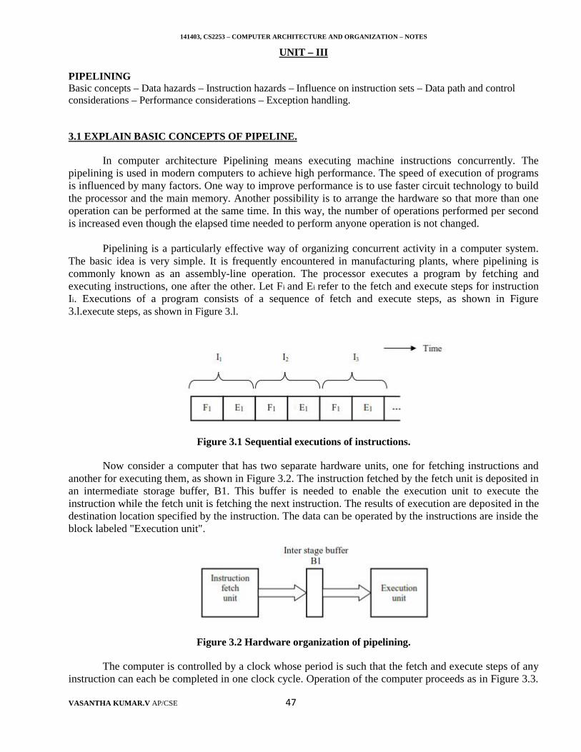
141403, CS2253 – COMPUTER ARCHITECTURE AND ORGANIZATION – NOTES
VASANTHA KUMAR.V AP/CSE 47
UNIT – III
PIPELININGBasic concepts – Data hazards – Instruction hazards – Influence on instruction sets – Data path and controlconsiderations – Performance considerations – Exception handling.
3.1 EXPLAIN BASIC CONCEPTS OF PIPELINE.
In computer architecture Pipelining means executing machine instructions concurrently. Thepipelining is used in modern computers to achieve high performance. The speed of execution of programsis influenced by many factors. One way to improve performance is to use faster circuit technology to buildthe processor and the main memory. Another possibility is to arrange the hardware so that more than oneoperation can be performed at the same time. In this way, the number of operations performed per secondis increased even though the elapsed time needed to perform anyone operation is not changed.
Pipelining is a particularly effective way of organizing concurrent activity in a computer system.The basic idea is very simple. It is frequently encountered in manufacturing plants, where pipelining iscommonly known as an assembly-line operation. The processor executes a program by fetching andexecuting instructions, one after the other. Let Fi and Ei refer to the fetch and execute steps for instructionIi. Executions of a program consists of a sequence of fetch and execute steps, as shown in Figure3.l.execute steps, as shown in Figure 3.l.
Figure 3.1 Sequential executions of instructions.
Now consider a computer that has two separate hardware units, one for fetching instructions andanother for executing them, as shown in Figure 3.2. The instruction fetched by the fetch unit is deposited inan intermediate storage buffer, B1. This buffer is needed to enable the execution unit to execute theinstruction while the fetch unit is fetching the next instruction. The results of execution are deposited in thedestination location specified by the instruction. The data can be operated by the instructions are inside theblock labeled "Execution unit".
Figure 3.2 Hardware organization of pipelining.
The computer is controlled by a clock whose period is such that the fetch and execute steps of anyinstruction can each be completed in one clock cycle. Operation of the computer proceeds as in Figure 3.3.
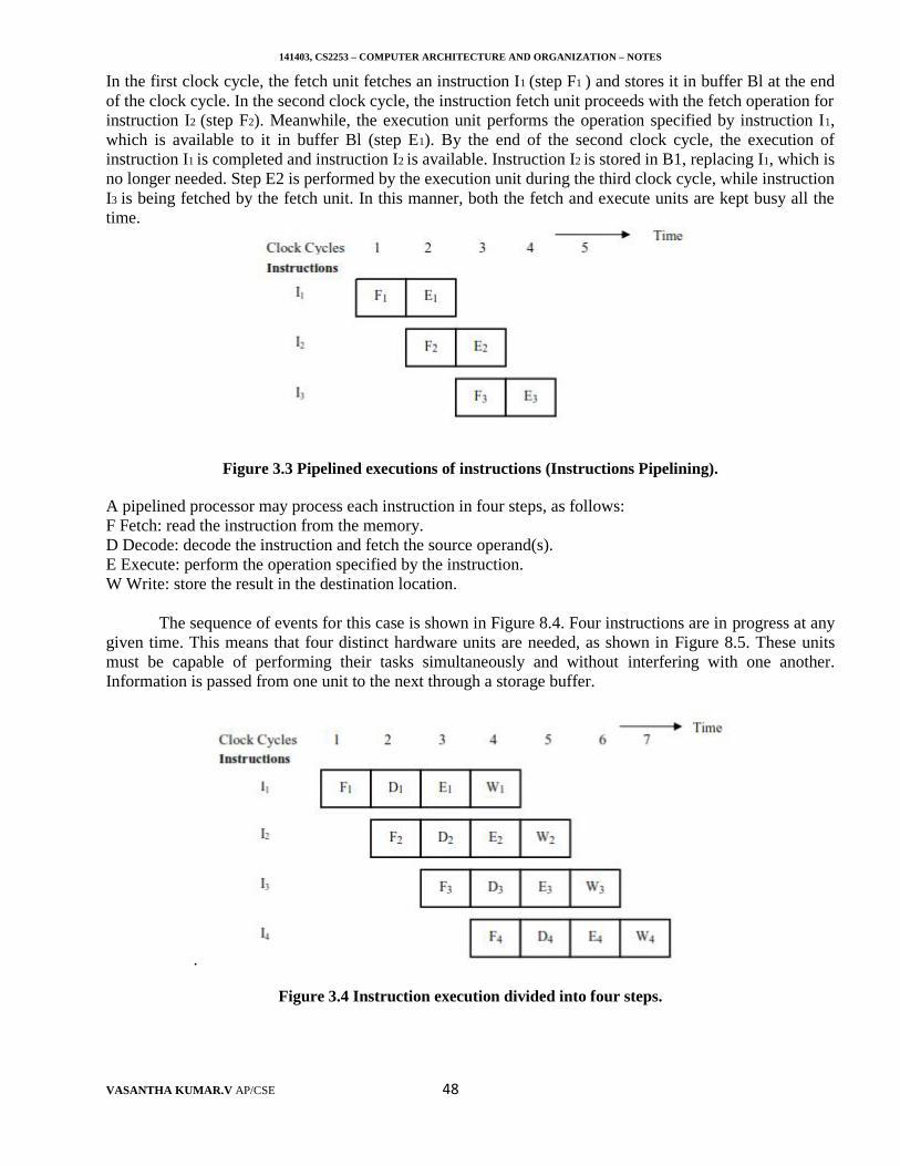
141403, CS2253 – COMPUTER ARCHITECTURE AND ORGANIZATION – NOTES
VASANTHA KUMAR.V AP/CSE 48
In the first clock cycle, the fetch unit fetches an instruction I1 (step F1 ) and stores it in buffer Bl at the endof the clock cycle. In the second clock cycle, the instruction fetch unit proceeds with the fetch operation forinstruction I2 (step F2). Meanwhile, the execution unit performs the operation specified by instruction I1,which is available to it in buffer Bl (step E1). By the end of the second clock cycle, the execution ofinstruction I1 is completed and instruction I2 is available. Instruction I2 is stored in B1, replacing I1, which isno longer needed. Step E2 is performed by the execution unit during the third clock cycle, while instructionI3 is being fetched by the fetch unit. In this manner, both the fetch and execute units are kept busy all thetime.
Figure 3.3 Pipelined executions of instructions (Instructions Pipelining).
A pipelined processor may process each instruction in four steps, as follows:F Fetch: read the instruction from the memory.D Decode: decode the instruction and fetch the source operand(s).E Execute: perform the operation specified by the instruction.W Write: store the result in the destination location.
The sequence of events for this case is shown in Figure 8.4. Four instructions are in progress at anygiven time. This means that four distinct hardware units are needed, as shown in Figure 8.5. These unitsmust be capable of performing their tasks simultaneously and without interfering with one another.Information is passed from one unit to the next through a storage buffer.
.
Figure 3.4 Instruction execution divided into four steps.
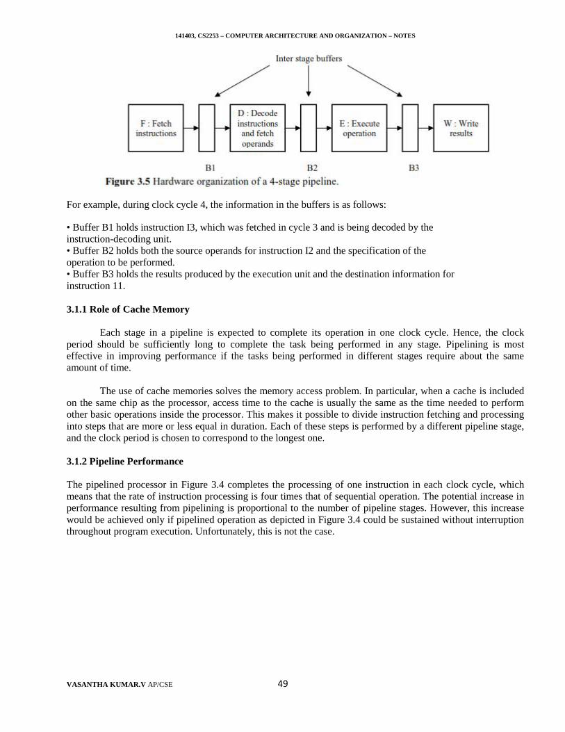
141403, CS2253 – COMPUTER ARCHITECTURE AND ORGANIZATION – NOTES
VASANTHA KUMAR.V AP/CSE 49
For example, during clock cycle 4, the information in the buffers is as follows:
• Buffer B1 holds instruction I3, which was fetched in cycle 3 and is being decoded by theinstruction-decoding unit.• Buffer B2 holds both the source operands for instruction I2 and the specification of theoperation to be performed.• Buffer B3 holds the results produced by the execution unit and the destination information forinstruction 11.
3.1.1 Role of Cache Memory
Each stage in a pipeline is expected to complete its operation in one clock cycle. Hence, the clockperiod should be sufficiently long to complete the task being performed in any stage. Pipelining is mosteffective in improving performance if the tasks being performed in different stages require about the sameamount of time.
The use of cache memories solves the memory access problem. In particular, when a cache is includedon the same chip as the processor, access time to the cache is usually the same as the time needed to performother basic operations inside the processor. This makes it possible to divide instruction fetching and processinginto steps that are more or less equal in duration. Each of these steps is performed by a different pipeline stage,and the clock period is chosen to correspond to the longest one.
3.1.2 Pipeline Performance
The pipelined processor in Figure 3.4 completes the processing of one instruction in each clock cycle, whichmeans that the rate of instruction processing is four times that of sequential operation. The potential increase inperformance resulting from pipelining is proportional to the number of pipeline stages. However, this increasewould be achieved only if pipelined operation as depicted in Figure 3.4 could be sustained without interruptionthroughout program execution. Unfortunately, this is not the case.
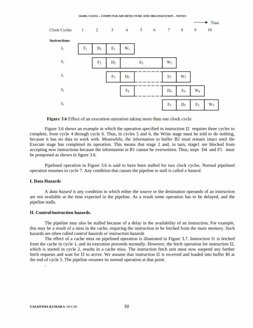
141403, CS2253 – COMPUTER ARCHITECTURE AND ORGANIZATION – NOTES
VASANTHA KUMAR.V AP/CSE 50
Figure 3.6 shows an example in which the operation specified in instruction I2 requires three cycles tocomplete, from cycle 4 through cycle 6. Thus, in cycles 5 and 6, the Write stage must be told to do nothing,because it has no data to work with. Meanwhile, the information in buffer B2 must remain intact until theExecute stage has completed its operation. This means that stage 2 and, in turn, stage1 are blocked fromaccepting new instructions because the information in B1 cannot be overwritten. Thus, steps D4 and F5 mustbe postponed as shown in figure 3.6.
Pipelined operation in Figure 3.6 is said to have been stalled for two clock cycles. Normal pipelinedoperation resumes in cycle 7. Any condition that causes the pipeline to stall is called a hazard.
I. Data Hazards
A data hazard is any condition in which either the source or the destination operands of an instructionare not available at the time expected in the pipeline. As a result some operation has to be delayed, and thepipeline stalls.
II. Control/instruction hazards.
The pipeline may also be stalled because of a delay in the availability of an instruction. For example,this may be a result of a miss in the cache, requiring the instruction to be fetched from the main memory. Suchhazards are often called control hazards or instruction hazards
The effect of a cache miss on pipelined operation is illustrated in Figure 3.7. Instruction I1 is fetchedfrom the cache in cycle 1, and its execution proceeds normally. However, the fetch operation for instruction I2,which is started in cycle 2, results in a cache miss. The instruction fetch unit must now suspend any furtherfetch requests and wait for I2 to arrive. We assume that instruction I2 is received and loaded into buffer Bl atthe end of cycle 5. The pipeline resumes its normal operation at that point.
.
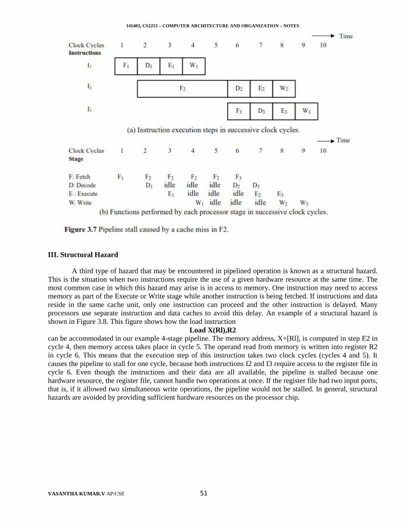
141403, CS2253 – COMPUTER ARCHITECTURE AND ORGANIZATION – NOTES
VASANTHA KUMAR.V AP/CSE 51
III. Structural Hazard
A third type of hazard that may be encountered in pipelined operation is known as a structural hazard.This is the situation when two instructions require the use of a given hardware resource at the same time. Themost common case in which this hazard may arise is in access to memory. One instruction may need to accessmemory as part of the Execute or Write stage while another instruction is being fetched. If instructions and datareside in the same cache unit, only one instruction can proceed and the other instruction is delayed. Manyprocessors use separate instruction and data caches to avoid this delay. An example of a structural hazard isshown in Figure 3.8. This figure shows how the load instruction
Load X(Rl),R2can be accommodated in our example 4-stage pipeline. The memory address, X+[Rl], is computed in step E2 incycle 4, then memory access takes place in cycle 5. The operand read from memory is written into register R2in cycle 6. This means that the execution step of this instruction takes two clock cycles (cycles 4 and 5). Itcauses the pipeline to stall for one cycle, because both instructions I2 and I3 require access to the register file incycle 6. Even though the instructions and their data are all available, the pipeline is stalled because onehardware resource, the register file, cannot handle two operations at once. If the register file had two input ports,that is, if it allowed two simultaneous write operations, the pipeline would not be stalled. In general, structuralhazards are avoided by providing sufficient hardware resources on the processor chip.
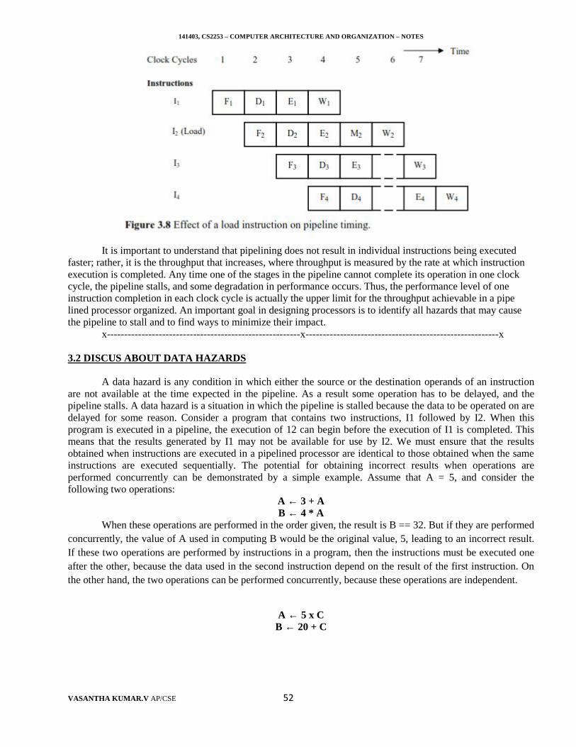
141403, CS2253 – COMPUTER ARCHITECTURE AND ORGANIZATION – NOTES
VASANTHA KUMAR.V AP/CSE 52
It is important to understand that pipelining does not result in individual instructions being executedfaster; rather, it is the throughput that increases, where throughput is measured by the rate at which instructionexecution is completed. Any time one of the stages in the pipeline cannot complete its operation in one clockcycle, the pipeline stalls, and some degradation in performance occurs. Thus, the performance level of oneinstruction completion in each clock cycle is actually the upper limit for the throughput achievable in a pipelined processor organized. An important goal in designing processors is to identify all hazards that may causethe pipeline to stall and to find ways to minimize their impact.
x--------------------------------------------------------x--------------------------------------------------------x
3.2 DISCUS ABOUT DATA HAZARDS
A data hazard is any condition in which either the source or the destination operands of an instructionare not available at the time expected in the pipeline. As a result some operation has to be delayed, and thepipeline stalls. A data hazard is a situation in which the pipeline is stalled because the data to be operated on aredelayed for some reason. Consider a program that contains two instructions, I1 followed by I2. When thisprogram is executed in a pipeline, the execution of 12 can begin before the execution of I1 is completed. Thismeans that the results generated by I1 may not be available for use by I2. We must ensure that the resultsobtained when instructions are executed in a pipelined processor are identical to those obtained when the sameinstructions are executed sequentially. The potential for obtaining incorrect results when operations areperformed concurrently can be demonstrated by a simple example. Assume that A = 5, and consider thefollowing two operations:
A ← 3 + AB ← 4 * A
When these operations are performed in the order given, the result is B == 32. But if they are performedconcurrently, the value of A used in computing B would be the original value, 5, leading to an incorrect result.If these two operations are performed by instructions in a program, then the instructions must be executed oneafter the other, because the data used in the second instruction depend on the result of the first instruction. Onthe other hand, the two operations can be performed concurrently, because these operations are independent.
A ← 5 x CB ← 20 + C
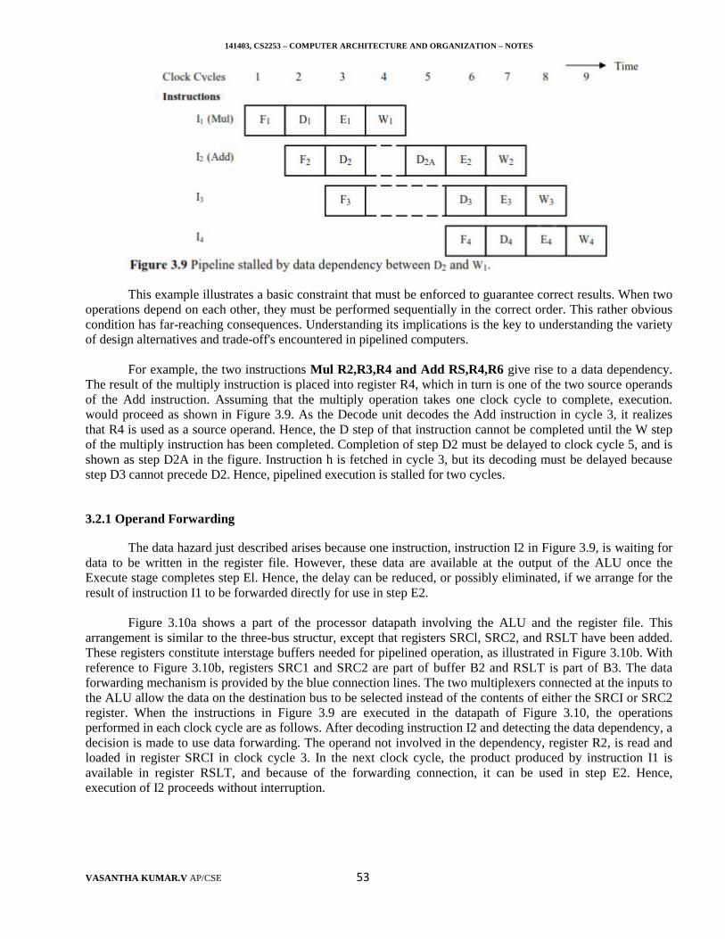
141403, CS2253 – COMPUTER ARCHITECTURE AND ORGANIZATION – NOTES
VASANTHA KUMAR.V AP/CSE 53
This example illustrates a basic constraint that must be enforced to guarantee correct results. When twooperations depend on each other, they must be performed sequentially in the correct order. This rather obviouscondition has far-reaching consequences. Understanding its implications is the key to understanding the varietyof design alternatives and trade-off's encountered in pipelined computers.
For example, the two instructions Mul R2,R3,R4 and Add RS,R4,R6 give rise to a data dependency.The result of the multiply instruction is placed into register R4, which in turn is one of the two source operandsof the Add instruction. Assuming that the multiply operation takes one clock cycle to complete, execution.would proceed as shown in Figure 3.9. As the Decode unit decodes the Add instruction in cycle 3, it realizesthat R4 is used as a source operand. Hence, the D step of that instruction cannot be completed until the W stepof the multiply instruction has been completed. Completion of step D2 must be delayed to clock cycle 5, and isshown as step D2A in the figure. Instruction h is fetched in cycle 3, but its decoding must be delayed becausestep D3 cannot precede D2. Hence, pipelined execution is stalled for two cycles.
3.2.1 Operand Forwarding
The data hazard just described arises because one instruction, instruction I2 in Figure 3.9, is waiting fordata to be written in the register file. However, these data are available at the output of the ALU once theExecute stage completes step El. Hence, the delay can be reduced, or possibly eliminated, if we arrange for theresult of instruction I1 to be forwarded directly for use in step E2.
Figure 3.10a shows a part of the processor datapath involving the ALU and the register file. Thisarrangement is similar to the three-bus structur, except that registers SRCl, SRC2, and RSLT have been added.These registers constitute interstage buffers needed for pipelined operation, as illustrated in Figure 3.10b. Withreference to Figure 3.10b, registers SRC1 and SRC2 are part of buffer B2 and RSLT is part of B3. The dataforwarding mechanism is provided by the blue connection lines. The two multiplexers connected at the inputs tothe ALU allow the data on the destination bus to be selected instead of the contents of either the SRCI or SRC2register. When the instructions in Figure 3.9 are executed in the datapath of Figure 3.10, the operationsperformed in each clock cycle are as follows. After decoding instruction I2 and detecting the data dependency, adecision is made to use data forwarding. The operand not involved in the dependency, register R2, is read andloaded in register SRCI in clock cycle 3. In the next clock cycle, the product produced by instruction I1 isavailable in register RSLT, and because of the forwarding connection, it can be used in step E2. Hence,execution of I2 proceeds without interruption.
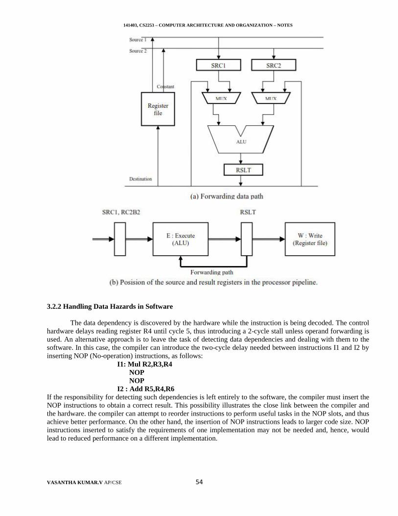
141403, CS2253 – COMPUTER ARCHITECTURE AND ORGANIZATION – NOTES
VASANTHA KUMAR.V AP/CSE 54
3.2.2 Handling Data Hazards in Software
The data dependency is discovered by the hardware while the instruction is being decoded. The controlhardware delays reading register R4 until cycle 5, thus introducing a 2-cycle stall unless operand forwarding isused. An alternative approach is to leave the task of detecting data dependencies and dealing with them to thesoftware. In this case, the compiler can introduce the two-cycle delay needed between instructions I1 and I2 byinserting NOP (No-operation) instructions, as follows:
I1: Mul R2,R3,R4NOPNOP
I2 : Add R5,R4,R6If the responsibility for detecting such dependencies is left entirely to the software, the compiler must insert theNOP instructions to obtain a correct result. This possibility illustrates the close link between the compiler andthe hardware. the compiler can attempt to reorder instructions to perform useful tasks in the NOP slots, and thusachieve better performance. On the other hand, the insertion of NOP instructions leads to larger code size. NOPinstructions inserted to satisfy the requirements of one implementation may not be needed and, hence, wouldlead to reduced performance on a different implementation.
141403, CS2253 – COMPUTER ARCHITECTURE AND ORGANIZATION – NOTES
VASANTHA KUMAR.V AP/CSE 55
3.2.3 Side Effect
The data dependencies encountered in the preceding examples are explicit and easily detected becausethe register involved is named as the destination in instruction I1 and as a source in I2. Sometimes an instructionchanges the contents of a register other than the one named as the destination. An instruction that uses anautoincrement or autodecrement addressing mode is an example. In addition to storing new data in itsdestination location, the instruction changes the contents of a source register used to access one of its operands.All the precautions needed to handle data dependencies involving the destination location must also be appliedto the registers affected by an autoincrement or autodecrement operation.
When a location other than one explicitly named in an instruction as a destination operand is affected,the instruction is said to have a side effect. For example, stack instructions, such as push and pop, producesimilar side effects because they implicitly use the autoincrement and autodecrement addressing modes.Another possible side effect involves the condition code flags, which are used by instructions such asconditional branches and add-with-carry. Suppose that registers Rl and R2 hold a double-precision integernumber that we wish to add to another double-precision number in registers R3 and R4. This may beaccomplished as follows:
Add Rl,R3AddWithCarry R2,R4
An implicit dependency exists between these two instructions through the carry flag. This flag is set bythe first instruction and used in the second instruction, which performs the operation.
R4 ← [R2] + [R4] + carryInstructions that have side effects give rise to multiple data dependencies, which lead to a substantial
increase in the complexity of the hardware or software needed to resolve them. For this reason, instructionsdesigned for execution on pipe lined hardware should have few side effects. Ideally, only the contents of thedestination location, either a register or a memory location, should be affected by any given instruction. Sideeffects, such as setting the condition code flags or updating the contents of an address pointer, should be kept toa minimum.
x--------------------------------------------------------x--------------------------------------------------------x
3.3 DISCUS ABOUT INSTRUCTION HAZARDS
Pipeline execution of instructions will reduce the time and improves the performance. Whenever thisstream is interrupted, the pipeline stalls, as figure 3.7 illustrates for the case of a cache miss. A branchinstruction may also cause the pipeline to stall. The effect of branch instructions and the techniques that can beused for mitigating their impact are discussed with unconditional branches and conditional branches.
3.3.1 Unconditional Branches
A sequence of instructions being executed in a two-stage pipeline is shown in Figure 3.11. InstructionsI1 to I3 are stored at successive memory addresses, and I2 is a branch instruction. Let the branch target beinstruction Ik. In clock cycle 3, the fetch operation for instruction 13 is in progress at the same time that thebranch instruction is being decoded and the target address computed. In clock cycle 4, the processor mustdiscard I3, which has been incorrectly fetched, and fetch instruction Ik. In the meantime, the hardware unitresponsible for the Execute (E) step must be told to do nothing during that clock period. Thus, the pipeline isstalled for one clock cycle.
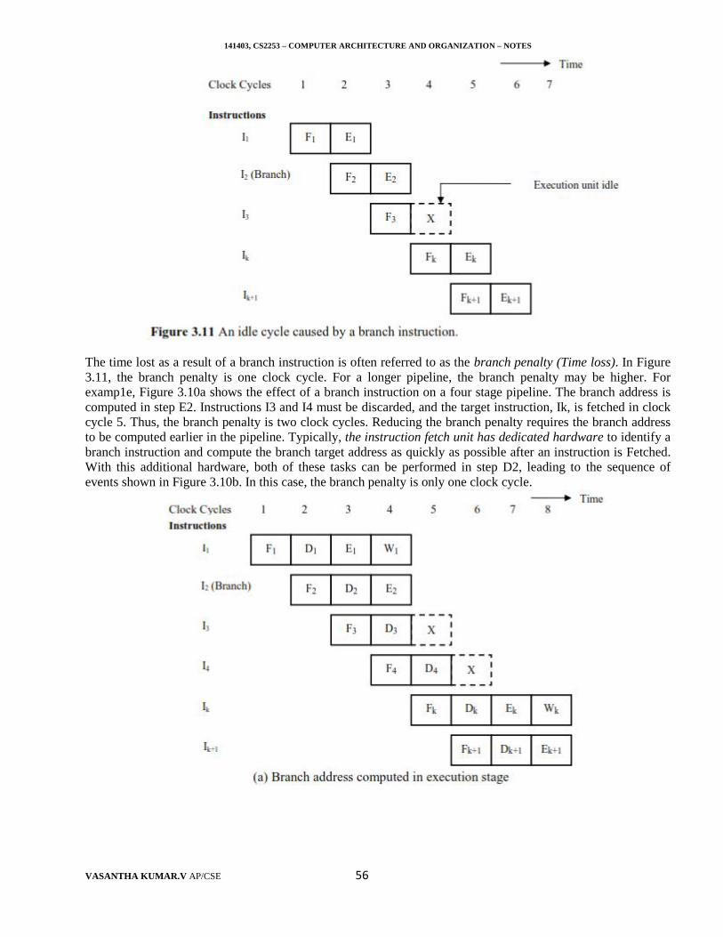
141403, CS2253 – COMPUTER ARCHITECTURE AND ORGANIZATION – NOTES
VASANTHA KUMAR.V AP/CSE 56
The time lost as a result of a branch instruction is often referred to as the branch penalty (Time loss). In Figure3.11, the branch penalty is one clock cycle. For a longer pipeline, the branch penalty may be higher. Forexamp1e, Figure 3.10a shows the effect of a branch instruction on a four stage pipeline. The branch address iscomputed in step E2. Instructions I3 and I4 must be discarded, and the target instruction, Ik, is fetched in clockcycle 5. Thus, the branch penalty is two clock cycles. Reducing the branch penalty requires the branch addressto be computed earlier in the pipeline. Typically, the instruction fetch unit has dedicated hardware to identify abranch instruction and compute the branch target address as quickly as possible after an instruction is Fetched.With this additional hardware, both of these tasks can be performed in step D2, leading to the sequence ofevents shown in Figure 3.10b. In this case, the branch penalty is only one clock cycle.
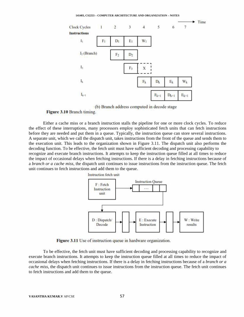
141403, CS2253 – COMPUTER ARCHITECTURE AND ORGANIZATION – NOTES
VASANTHA KUMAR.V AP/CSE 57
Either a cache miss or a branch instruction stalls the pipeline for one or more clock cycles. To reducethe effect of these interruptions, many processors employ sophisticated fetch units that can fetch instructionsbefore they are needed and put them in a queue. Typically, the instruction queue can store several instructions.A separate unit, which we call the dispatch unit, takes instructions from the front of the queue and sends them tothe execution unit. This leads to the organization shown in Figure 3.11. The dispatch unit also performs thedecoding function. To be effective, the fetch unit must have sufficient decoding and processing capability torecognize and execute branch instructions. It attempts to keep the instruction queue filled at all times to reducethe impact of occasional delays when fetching instructions. If there is a delay in fetching instructions because ofa branch or a cache miss, the dispatch unit continues to issue instructions from the instruction queue. The fetchunit continues to fetch instructions and add them to the queue.
To be effective, the fetch unit must have sufficient decoding and processing capability to recognize andexecute branch instructions. It attempts to keep the instruction queue filled at all times to reduce the impact ofoccasional delays when fetching instructions. If there is a delay in fetching instructions because of a branch or acache miss, the dispatch unit continues to issue instructions from the instruction queue. The fetch unit continuesto fetch instructions and add them to the queue.
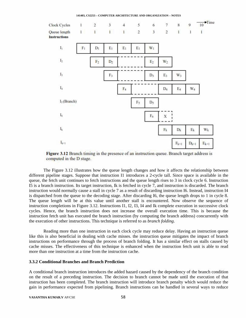
141403, CS2253 – COMPUTER ARCHITECTURE AND ORGANIZATION – NOTES
VASANTHA KUMAR.V AP/CSE 58
The Figure 3.12 illustrates how the queue length changes and how it affects the relationship betweendifferent pipeline stages. Suppose that instruction I1 introduces a 2-cycle tall. Since space is available in thequeue, the fetch unit continues to fetch instructions and the queue length rises to 3 in clock cycle 6. InstructionI5 is a branch instruction. Its target instruction, Ik is fetched in cycle 7, and instruction is discarded. The branchinstruction would normally cause a stall in cycle 7 as a result of discarding instruction I6. Instead, instruction I4is dispatched from the queue to the decoding stage. After discarding I6, the queue length drops to 1 in cycle 8.The queue length will be at this value until another stall is encountered. Now observe the sequence ofinstruction completions in Figure 3.12. Instructions I1, I2, I3, I4 and Ik complete execution in successive clockcycles. Hence, the branch instruction does not increase the overall execution time. This is because theinstruction fetch unit has executed the branch instruction (by computing the branch address) concurrently withthe execution of other instructions. This technique is referred to as branch folding.
Reading more than one instruction in each clock cycle may reduce delay. Having an instruction queuelike this is also beneficial in dealing with cache misses. the instruction queue mitigates the impact of branchinstructions on performance through the process of branch folding. It has a similar effect on stalls caused bycache misses. The effectiveness of this technique is enhanced when the instruction fetch unit is able to readmore than one instruction at a time from the instruction cache.
3.3.2 Conditional Branches and Branch Prediction
A conditional branch instruction introduces the added hazard caused by the dependency of the branch conditionon the result of a preceding instruction. The decision to branch cannot be made until the execution of thatinstruction has been completed. The branch instruction will introduce branch penalty which would reduce thegain in performance expected from pipelining. Branch instructions can be handled in several ways to reduce
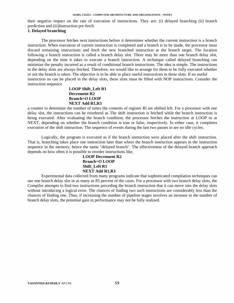
141403, CS2253 – COMPUTER ARCHITECTURE AND ORGANIZATION – NOTES
VASANTHA KUMAR.V AP/CSE 59
their negative impact on the rate of execution of instructions. They are: (i) delayed branching (ii) branchprediction and (iii)Instruction pre-fetch.1. Delayed branching
The processor fetches next instructions before it determines whether the current instruction is a branchinstruction. When execution of current instruction is completed and a branch is to be made, the processor mustdiscard remaining instructions and fetch the new branched instruction at the branch target. The locationfollowing a branch instruction is called a branch delay slot. There may be more than one branch delay slot,depending on the time it takes to execute a branch instruction. A technique called delayed branching canminimize the penalty incurred as a result of conditional branch instructions. The idea is simple. The instructionsin the delay slots are always fetched. Therefore, we would like to arrange for them to be fully executed whetheror not the branch is taken. The objective is to be able to place useful instructions in these slots. If no usefulinstruction ns can be placed in the delay slots, these slots must be filled with NOP instructions. Consider theinstruction sequence
LOOP Shift_Left R1Decrement R2Branch=O LOOPNEXT Add R1,R3
a counter to determine the number of times the contents of register Rl are shifted left. For a processor with onedelay slot, the instructions can be reordered as The shift instruction is fetched while the branch instruction isbeing executed. After evaluating the branch condition, the processor fetches the instruction at LOOP or atNEXT, depending on whether the branch condition is true or false, respectively. In either case, it completesexecution of the shift instruction. The sequence of events during the last two passes in are no idle cycles.
Logically, the program is executed as if the branch instruction were placed after the shift instruction.That is, branching takes place one instruction later than where the branch instruction appears in the instructionsequence in the memory, hence the name "delayed branch". The effectiveness of the delayed branch approachdepends on how often it is possible to reorder instructions like,
LOOP Decrement R2Branch=O LOOPShift_Left R1NEXT Add R1,R3
Experimental data collected from many programs indicate that sophisticated compilation techniques canuse one branch delay slot in as many as 85 percent of the cases. For a processor with two branch delay slots, theCompiler attempts to find two instructions preceding the branch instruction that it can move into the delay slotswithout introducing a logical error. The chances of finding two such instructions are considerably less than thechances of finding one. Thus, if increasing the number of pipeline stages involves an increase in the number ofbranch delay slots, the potential gain in performance may not be fully realized.
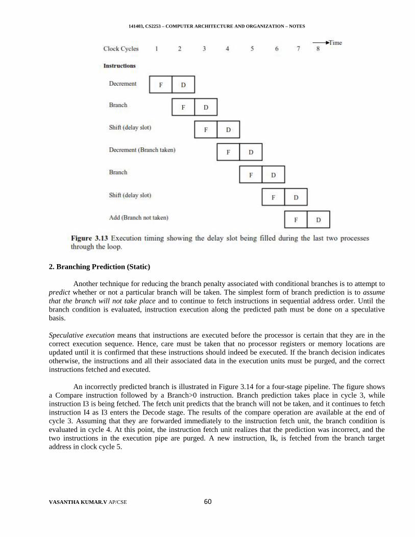
141403, CS2253 – COMPUTER ARCHITECTURE AND ORGANIZATION – NOTES
VASANTHA KUMAR.V AP/CSE 60
2. Branching Prediction (Static)
Another technique for reducing the branch penalty associated with conditional branches is to attempt topredict whether or not a particular branch will be taken. The simplest form of branch prediction is to assumethat the branch will not take place and to continue to fetch instructions in sequential address order. Until thebranch condition is evaluated, instruction execution along the predicted path must be done on a speculativebasis.
Speculative execution means that instructions are executed before the processor is certain that they are in thecorrect execution sequence. Hence, care must be taken that no processor registers or memory locations areupdated until it is confirmed that these instructions should indeed be executed. If the branch decision indicatesotherwise, the instructions and all their associated data in the execution units must be purged, and the correctinstructions fetched and executed.
An incorrectly predicted branch is illustrated in Figure 3.14 for a four-stage pipeline. The figure showsa Compare instruction followed by a Branch>0 instruction. Branch prediction takes place in cycle 3, whileinstruction I3 is being fetched. The fetch unit predicts that the branch will not be taken, and it continues to fetchinstruction I4 as I3 enters the Decode stage. The results of the compare operation are available at the end ofcycle 3. Assuming that they are forwarded immediately to the instruction fetch unit, the branch condition isevaluated in cycle 4. At this point, the instruction fetch unit realizes that the prediction was incorrect, and thetwo instructions in the execution pipe are purged. A new instruction, Ik, is fetched from the branch targetaddress in clock cycle 5.
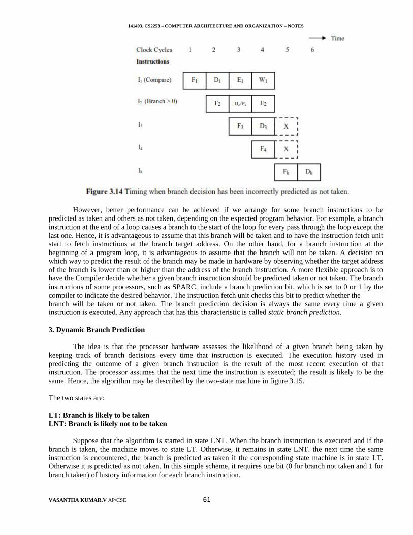
141403, CS2253 – COMPUTER ARCHITECTURE AND ORGANIZATION – NOTES
VASANTHA KUMAR.V AP/CSE 61
However, better performance can be achieved if we arrange for some branch instructions to bepredicted as taken and others as not taken, depending on the expected program behavior. For example, a branchinstruction at the end of a loop causes a branch to the start of the loop for every pass through the loop except thelast one. Hence, it is advantageous to assume that this branch will be taken and to have the instruction fetch unitstart to fetch instructions at the branch target address. On the other hand, for a branch instruction at thebeginning of a program loop, it is advantageous to assume that the branch will not be taken. A decision onwhich way to predict the result of the branch may be made in hardware by observing whether the target addressof the branch is lower than or higher than the address of the branch instruction. A more flexible approach is tohave the Compiler decide whether a given branch instruction should be predicted taken or not taken. The branchinstructions of some processors, such as SPARC, include a branch prediction bit, which is set to 0 or 1 by thecompiler to indicate the desired behavior. The instruction fetch unit checks this bit to predict whether thebranch will be taken or not taken. The branch prediction decision is always the same every time a giveninstruction is executed. Any approach that has this characteristic is called static branch prediction.
3. Dynamic Branch Prediction
The idea is that the processor hardware assesses the likelihood of a given branch being taken bykeeping track of branch decisions every time that instruction is executed. The execution history used inpredicting the outcome of a given branch instruction is the result of the most recent execution of thatinstruction. The processor assumes that the next time the instruction is executed; the result is likely to be thesame. Hence, the algorithm may be described by the two-state machine in figure 3.15.
The two states are:
LT: Branch is likely to be takenLNT: Branch is likely not to be taken
Suppose that the algorithm is started in state LNT. When the branch instruction is executed and if thebranch is taken, the machine moves to state LT. Otherwise, it remains in state LNT. the next time the sameinstruction is encountered, the branch is predicted as taken if the corresponding state machine is in state LT.Otherwise it is predicted as not taken. In this simple scheme, it requires one bit (0 for branch not taken and 1 forbranch taken) of history information for each branch instruction.
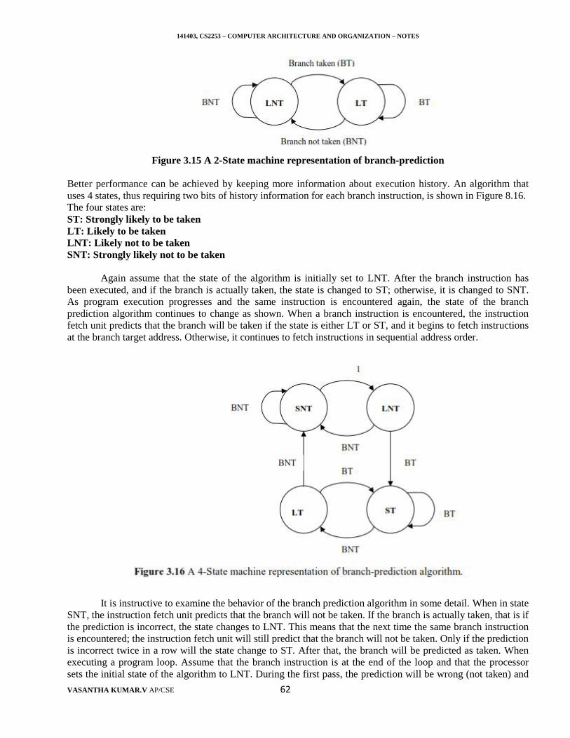
141403, CS2253 – COMPUTER ARCHITECTURE AND ORGANIZATION – NOTES
VASANTHA KUMAR.V AP/CSE 62
Figure 3.15 A 2-State machine representation of branch-prediction
Better performance can be achieved by keeping more information about execution history. An algorithm thatuses 4 states, thus requiring two bits of history information for each branch instruction, is shown in Figure 8.16.The four states are:ST: Strongly likely to be takenLT: Likely to be takenLNT: Likely not to be takenSNT: Strongly likely not to be taken
Again assume that the state of the algorithm is initially set to LNT. After the branch instruction hasbeen executed, and if the branch is actually taken, the state is changed to ST; otherwise, it is changed to SNT.As program execution progresses and the same instruction is encountered again, the state of the branchprediction algorithm continues to change as shown. When a branch instruction is encountered, the instructionfetch unit predicts that the branch will be taken if the state is either LT or ST, and it begins to fetch instructionsat the branch target address. Otherwise, it continues to fetch instructions in sequential address order.
It is instructive to examine the behavior of the branch prediction algorithm in some detail. When in stateSNT, the instruction fetch unit predicts that the branch will not be taken. If the branch is actually taken, that is ifthe prediction is incorrect, the state changes to LNT. This means that the next time the same branch instructionis encountered; the instruction fetch unit will still predict that the branch will not be taken. Only if the predictionis incorrect twice in a row will the state change to ST. After that, the branch will be predicted as taken. Whenexecuting a program loop. Assume that the branch instruction is at the end of the loop and that the processorsets the initial state of the algorithm to LNT. During the first pass, the prediction will be wrong (not taken) and
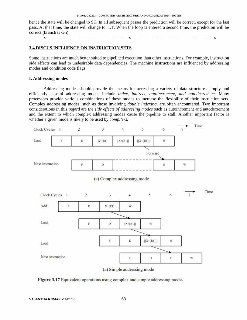
141403, CS2253 – COMPUTER ARCHITECTURE AND ORGANIZATION – NOTES
VASANTHA KUMAR.V AP/CSE 63
hence the state will be changed to ST. In all subsequent passes the prediction will be correct, except for the lastpass. At that time, the state will change to LT. When the loop is entered a second time, the prediction will becorrect (branch taken).
x--------------------------------------------------------x--------------------------------------------------------x
3.4 DISCUS INFLUENCE ON INSTRUCTION SETS
Some instructions are much better suited to pipelined execution than other instructions. For example, instructionside effects can lead to undesirable data dependencies. The machine instructions are influenced by addressingmodes and condition code flags.
I. Addressing modes
Addressing modes should provide the means for accessing a variety of data structures simply andefficiently. Useful addressing modes include index, indirect, autoincrement, and autodecrement. Manyprocessors provide various combinations of these modes to increase the flexibility of their instruction sets.Complex addressing modes, such as those involving double indexing, are often encountered. Two importantconsiderations in this regard are the side effects of addressing modes such as autoincrement and autodecrementand the extent to which complex addressing modes cause the pipeline to stall. Another important factor iswhether a given mode is likely to be used by compilers.
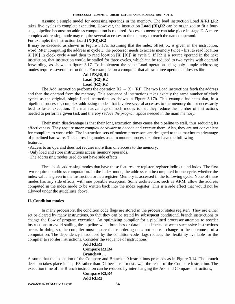
141403, CS2253 – COMPUTER ARCHITECTURE AND ORGANIZATION – NOTES
VASANTHA KUMAR.V AP/CSE 64
Assume a simple model for accessing operands in the memory. The load instruction Load X(RI ),R2takes five cycles to complete execution, However, the instruction Load (Rl),R2 can be organized to fit a four-stage pipeline because no address computation is required. Access to memory can take place in stage E. A morecomplex addressing mode may require several accesses to the memory to reach the named operand.For example, the instruction Load (X(Rl)),R2It may be executed as shown in Figure 3.17a, assuming that the index offset, X, is given in the instruction,word. Mter computing the address in cycle 3, the processor needs to access memory twice - first to read locationX+[Rl] in clock cycle 4 and then to read location [X+[Rl]] in cycle 5. If R2 is a source operand in the nextinstruction, that instruction would be stalled for three cycles, which can be reduced to two cycles with operandforwarding, as shown in figure 3.17. To implement the same Load operation using only simple addressingmodes requires several instructions. For example, on a computer that allows three operand addresses like
Add #X,Rl,R2Load (R2),R2Load (R2),R2
The Add instruction performs the operation R2 ← X+ [RI], The two Load instructions fetch the addressand then the operand from the memory. This sequence of instructions takes exactly the same number of clockcycles as the original, single Load instruction, as shown in Figure 3.17b. This example indicates that, in apipelined processor, complex addressing modes that involve several accesses to the memory do not necessarilylead to faster execution. The main advantage of such modes is that they reduce the number of instructionsneeded to perform a given task and thereby reduce the program space needed in the main memory.
Their main disadvantage is that their long execution times cause the pipeline to stall, thus reducing itseffectiveness. They require more complex hardware to decode and execute them. Also, they are not convenientfor compilers to work with. The instruction sets of modem processors are designed to take maximum advantageof pipelined hardware. The addressing modes used in modem processors often have the followingfeatures:· Access to an operand does not require more than one access to the memory.· Only load and store instructions access memory operands.· The addressing modes used do not have side effects.
Three basic addressing modes that have these features are register, register indirect, and index. The firsttwo require no address computation. In the index mode, the address can be computed in one cycle, whether theindex value is given in the instruction or in a register. Memory is accessed in the following cycle. None of thesemodes has any side effects, with one possible exception. Some architecture, such as ARM, allow the addresscomputed in the index mode to be written back into the index register. This is a side effect that would not beallowed under the guidelines above.
II. Condition modes
In many processors, the condition code flags are stored in the processor status register. They are eitherset or cleared by many instructions, so that they can be tested by subsequent conditional branch instructions tochange the flow of program execution. An optimizing compiler for a pipelined processor attempts to reorderinstructions to avoid stalling the pipeline when branches or data dependencies between successive instructionsoccur. In doing so, the compiler must ensure that reordering does not cause a change in the outcome e of acomputation. The dependency introduced by the condition-code flags reduces the flexibility available for thecompiler to reorder instructions. Consider the sequence of instructions
Add Rl,R2Compare R3,R4Branch=0 …
Assume that the execution of the Compare and Branch = 0 instructions proceeds as in Figure 3.14. The branchdecision takes place in step E3 rather than D2 because it must await the result of the Compare instruction. Theexecution time of the Branch instruction can be reduced by interchanging the Add and Compare instructions,
Compare R3,R4Add Rl,R2
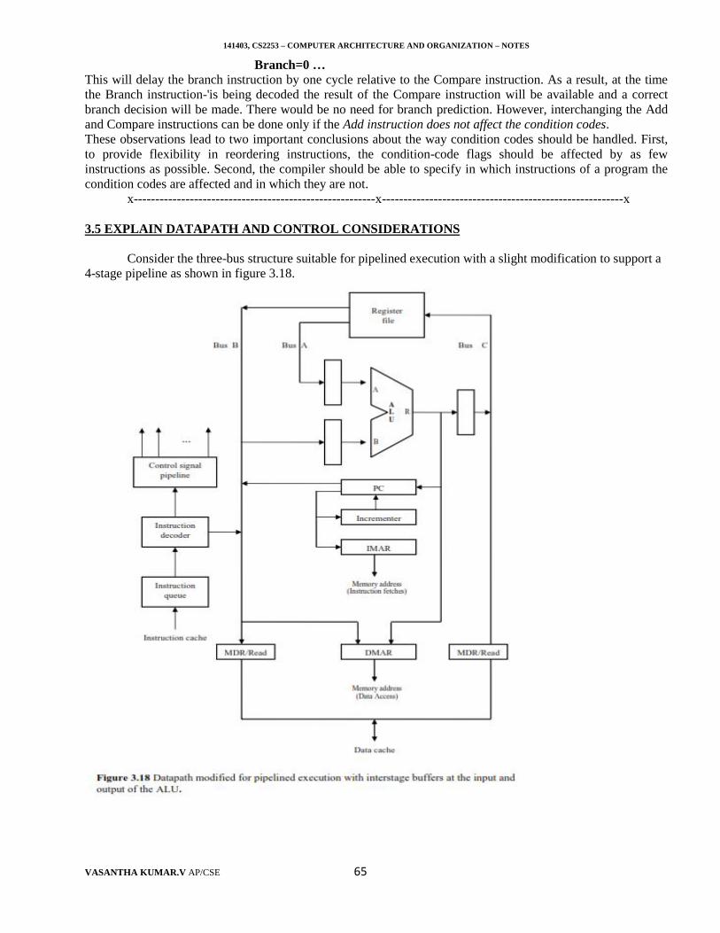
141403, CS2253 – COMPUTER ARCHITECTURE AND ORGANIZATION – NOTES
VASANTHA KUMAR.V AP/CSE 65
Branch=0 …This will delay the branch instruction by one cycle relative to the Compare instruction. As a result, at the timethe Branch instruction-'is being decoded the result of the Compare instruction will be available and a correctbranch decision will be made. There would be no need for branch prediction. However, interchanging the Addand Compare instructions can be done only if the Add instruction does not affect the condition codes.These observations lead to two important conclusions about the way condition codes should be handled. First,to provide flexibility in reordering instructions, the condition-code flags should be affected by as fewinstructions as possible. Second, the compiler should be able to specify in which instructions of a program thecondition codes are affected and in which they are not.
x--------------------------------------------------------x--------------------------------------------------------x
3.5 EXPLAIN DATAPATH AND CONTROL CONSIDERATIONS
Consider the three-bus structure suitable for pipelined execution with a slight modification to support a4-stage pipeline as shown in figure 3.18.
141403, CS2253 – COMPUTER ARCHITECTURE AND ORGANIZATION – NOTES
VASANTHA KUMAR.V AP/CSE 66
Several important changes are1. There are separate instruction and data caches that use separate address and data connections to theprocessor. This requires two versions of the MAR register, IMAR for accessing tile instruction cache andDMAR for accessing the data cache.2. The PC is connected directly to the IMAR, so that the contents of the PC can be transferred to IMAR at thesame time that an independent ALU operation is taking place.3. The data address in DMAR can be obtained directly from the register file or from the ALU to support theregister indirect and indexed addressing modes.4. Separate MDR registers are provided for read and write operations. Data can be transferred directly betweenthese registers and the register file during load and store operations without the need to pass through the ALU.5. Buffer registers have been introduced at the inputs and output of the ALU. These are registers SRCl, SRC2,and RSLT. Forwarding connections may be added if desired.6. The instruction register has been replaced with an instruction queue, which is loaded from the instructioncache.7. The output of the instruction decoder is connected to the control signal pipeline. This pipeline holds thecontrol signals in buffers B2 and B3 in Figure 3.3.
The following operations can be performed independently in the processor of Figure 3.18:
• Reading an instruction from the instruction cache• Incrementing the PC• Decoding an instruction• Reading from or writing into the data cache• Reading the contents of up to two registers from the register file• Writing into one register in the register file• Performing an ALU operation
x--------------------------------------------------------x--------------------------------------------------------x
3.6 EXPLAIN PERFORMANCE CONSIDERATION
The processor execution time T, of a program that has a dynamic instruction count N is given by
Where S is the average number of clock cycles it takes to fetch and execute one instruction and R is the clockrate. This simple model assumes that instructions are executed one after the other, with no overlap. A usefulperformance indicator is the instruction throughput, which is the number of instructions executed per second.For sequential execution, the throughput, Ps is given by
In general, an n-stage pipeline has the potential to increase throughput n times. Thus, it would appearthat the higher the value of n, the larger the performances gain. Any time a pipeline is stalled, the instructionthroughput is reduced. Hence, the performance of a pipeline is highly influenced by factors such as branch andcache miss penalties.
I. Effect Of Instruction Hazards
Consider a processor that uses the four-stage pipeline. The time (clock rate) allocated to each step in thepipeline is determined by the longest step. Let the delay through the ALU be the critical parameter. This is thetime needed to add two integers. Thus, if the ALU delay is 2 ns, a clock of 500 MHz can be used. The on-chipinstruction and data caches for this processor should also be designed to have an access time of 2 ns. Underideal conditions, this pipe lined processor will have an instruction throughput, Pp, given by
141403, CS2253 – COMPUTER ARCHITECTURE AND ORGANIZATION – NOTES
VASANTHA KUMAR.V AP/CSE 67
Pp = R = 500 MIPS (million instructions per second)To evaluate the effect of cache misses, the cache miss penalty, Mp, in that system is computed to be 17
clock cycles. Let TI be the time between two successive instruction completions. For sequential execution, TI =S. However, in the absence of hazards, a pipelined processor completes the execution of one instruction eachclock cycle, thus, TI = 1 cycle. A cache miss stalls the pipeline by an amount equal to the cache miss penalty.This means that the value of TI increases by an amount equal to the cache miss penalty for the instruction inwhich the miss occurs. A cache miss can occur for either instructions or data. Consider a computer that has ashared cache for both instructions and data, and let d be the percentage of instructions that refer to data operandsin the memory. The average increase in the value of TI as a result of cache misses is given by
δmiss = ((1 - hi) + d(l - hd )) x Mpwhere hi and hd are the hit ratios for instructions and data, respectively. Assume that 30 percent of theinstructions access data in memory. With a 95-percent instruction hit rate and a 90 percent data hit rate, δmiss isgiven by
δmiss = (0.05 + 0.3 x 0.1) x 17 = 1.36 cyclesTaking this delay into account, the processor's throughput would be
Note that with R expressed in MHz, the throughput is obtained directly in minions of instructions persecond. For R = 500 MHz, Pp = 210 MIPS. Let us compare this value to the throughput obtainable withoutpipelining. A processor that uses sequential execution requires four cycles per instruction. Its throughput wouldbe
For R = 500 MHz, Ps = 95 MIPs. Clearly, pipelining leads to significantly higher throughput. But theperformance gain of 0.42/0.19 = 2.2 is only slightly better than one-half the ideal case. Reducing the cache misspenalty is particularly worthwhile in a pipelined processor. This can be achieved by introducing a secondarycache between the primary, on-chip cache and the memory. Assume that the time needed to transfer an 8-wordblock from the secondary cache is 10ns. Hence, a miss in the primary cache for which the required block isfound in the secondary cache introduces a penalty, Ms, of 5 cycles. In the case of a miss in the secondary cache,the full 17-cycle penalty (Mp) is still incurred. Hence, assuming a hit rate hs of 94 percent in the secondarycache, the average increase in TI is
δmiss = (1 - hi ) + d(1 - hd )) x (hs x Ms + (1 - hs) x M p ) = 0.46 cycleThe instruction throughput in this case is 0.68R, or 340 MIPS. An equivalent non pipelined processor
would have a throughput ofO.22R, or 110 MIPS. Thus, pipelining provides a performance gain of 0.68/0.22 =3.1.
The values of 1.36 and 0.46 are somewhat pessimistic, because it is assumed that every time a data missoccurs, the entire miss penalty is incurred. This is the case only if the instruction immediately following theinstruction that references memory is delayed while the processor waits for the memory access to be completed.However, an optimizing compiler attempts to increase the distance between two instructions that create adependency by placing other instructions between them whenever possible. Also, in a processor that uses aninstruction queue, the cache miss penalty during instruction fetches may have a much reduced effect as theprocessor is able to dispatch instructions from the queue.
I. Number Of Pipeline Stages
The fact that an n-stage pipeline may increase instruction throughput by a factor of n suggests that weshould use a large number of stages. However, as the number of pipeline stages increases, so does theprobability of the pipeline being stalled, because more instructions are being executed concurrently. Thus,dependencies between instructions that are far apart may still cause the pipeline to stall. Also, branch penalties
141403, CS2253 – COMPUTER ARCHITECTURE AND ORGANIZATION – NOTES
VASANTHA KUMAR.V AP/CSE 68
may become more significant. For these reasons, the gain from increasing the value of n begins to diminish, andthe associated cost is not justified. Another important factor is the inherent delay in the basic operationsperformed by the processor. The most important among these is the ALU delay.
In many processors, the cycle time of the processor clock is chosen such that one ALU operation can becompleted in one cycle. Other operations are divided into steps that take about the same time as an addoperation. It is also possible to use a pipelined ALU. For example, the ALU of the Compaq Alpha 21064processor consists of a two-stage pipeline, in which each stage completes its operation in 5 ns. Many pipelinedprocessors use four to six stages. Others divide instruction execution into smaller steps and use more pipelinestages and a faster clock. For example, the UltraSPARC II uses a 9-stage pipeline and Intel's Pentium Pro uses a12-stagepipeline. The latest Intel processor, Pentium 4, has a 20-stage pipeline and uses a clock speed in therange 1.3 to 1.5 GHz. For fast operations, there are two pipeline stages in one clock cycle.
x--------------------------------------------------------x--------------------------------------------------------x3.7 DISCUSS EXCEPTION HANDLING
I. Superscalar Operation
Pipelining makes it possible to execute instructions concurrently. Several instructions are present in thepipeline at the same time, but they are in different stages of their execution. While one instruction is performingan ALU operation, another instruction is being decoded and yet another is being fetched from the memory.Instructions enter the pipeline in strict program order. In the absence of hazards, one instruction enters thepipeline and one instruction completes execution in each clock cycle. This means that the maximum throughputof a pipelined processor is one instruction per clock cycle.
A more aggressive approach is to equip the processor with multiple processing units to handle severalinstructions in parallel in each processing stage. With this arrangement, several instructions start execution inthe same clock cycle, and the processor is said to use multiple-issue. Such processors are capable of achievingan instruction execution throughput of more than one instruction per cycle. They are known as superscalarprocessors. Many modem high-performance processors use this approach.
The instruction queue filled is introduced, so that a processor should be able to fetch more than oneinstruction at a time from the cache. For superscalar operation, this arrangement is essential. Multiple-issueoperation requires a wider path to the cache and multiple execution units. Separate execution units are providedfor integer and floating-point instructions.
Figure 8.19 shows an example of a processor with two execution units, one for integer and one for floating-point operations. The Instruction fetch unit is capable of reading two instructions at a time and storing them inthe instruction queue. In each clock cycle, the Dispatch unit retrieves and decodes up to two instructions fromthe front of the queue. If there is one integer, one floatingpoint instruction, and no hazards, both instructions aredispatched in the same clock cycle. In a superscalar processor, the detrimental effect on performance of varioushazards becomes even more pronounced. The compiler can avoid many hazards through judicious selection andordering of instructions. For example, for the processor in Figure 3.19, the compiler should strive to interleavefloating-point and integer instructions. This would enable the dispatch unit to keep both the integer and floating-point units busy most of the time. In general, high performance is achieved if the compiler is able to arrangeprogram instructions to take maximum advantage of the available hardware units.
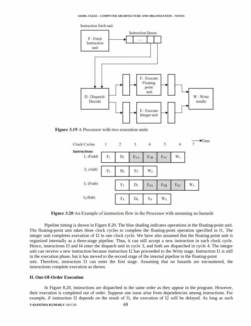
141403, CS2253 – COMPUTER ARCHITECTURE AND ORGANIZATION – NOTES
VASANTHA KUMAR.V AP/CSE 69
Pipeline timing is shown in Figure 8.20. The blue shading indicates operations in the floating-point unit.The floating-point unit takes three clock cycles to complete the floating-point operation specified in I1. Theinteger unit completes execution of I2 in one clock cycle. We have also assumed that the floating-point unit isorganized internally as a three-stage pipeline. Thus, it can still accept a new instruction in each clock cycle.Hence, instructions I3 and I4 enter the dispatch unit in cycle 3, and both are dispatched in cycle 4. The integerunit can receive a new instruction because instruction I2 has proceeded to the Write stage. Instruction I1 is stillin the execution phase, but it has moved to the second stage of the internal pipeline in the floating-pointunit. Therefore, instruction I3 can enter the first stage. Assuming that no hazards are encountered, theinstructions complete execution as shown.
II. Out-Of-Order Execution
In Figure 8.20, instructions are dispatched in the same order as they appear in the program. However,their execution is completed out of order. Suppose one issue arise from dependencies among instructions. Forexample, if instruction I2 depends on the result of I1, the execution of I2 will be delayed. As long as such
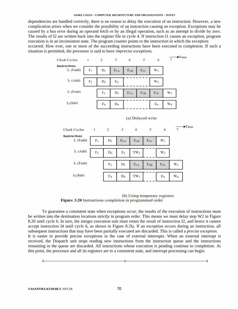
141403, CS2253 – COMPUTER ARCHITECTURE AND ORGANIZATION – NOTES
VASANTHA KUMAR.V AP/CSE 70
dependencies are handled correctly, there is no reason to delay the execution of an instruction. However, a newcomplication arises when we consider the possibility of an instruction causing an exception. Exceptions may becaused by a bus error during an operand fetch or by an illegal operation, such as an attempt to divide by zero.The results of I2 are written back into the register file in cycle 4. If instruction I1 causes an exception, programexecution is in an inconsistent state. The program counter points to the instruction in which the exceptionoccurred. How ever, one or more of the succeeding instructions have been executed to completion. If such asituation is permitted, the processor is said to have imprecise exceptions.
To guarantee a consistent state when exceptions occur, the results of the execution of instructions mustbe written into the destination locations strictly in program order. This means we must delay step W2 in Figure8.20 until cycle 6. In turn, the integer execution unit must retain the result of instruction I2, and hence it cannotaccept instruction I4 until cycle 6, as shown in Figure 8.2Ia. If an exception occurs during an instruction, allsubsequent instructions that may have been partially executed are discarded. This is called a precise exception.It is easier to provide precise exceptions in the case of external interrupts. When an external interrupt isreceived, the Dispatch unit stops reading new instructions from the instruction queue and the instructionsremaining in the queue are discarded. All instructions whose execution is pending continue to completion. Atthis point, the processor and all its registers are in a consistent state, and interrupt processing can begin.
x--------------------------------------------------------x--------------------------------------------------------x
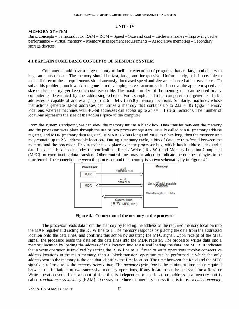
141403, CS2253 – COMPUTER ARCHITECTURE AND ORGANIZATION – NOTES
VASANTHA KUMAR.V AP/CSE 71
UNIT - IVMEMORY SYSTEMBasic concepts – Semiconductor RAM – ROM – Speed – Size and cost – Cache memories – Improving cacheperformance – Virtual memory – Memory management requirements – Associative memories – Secondarystorage devices.
4.1 EXPLAIN SOME BASIC CONCEPTS OF MEMORY SYSTEM
Computer should have a large memory to facilitate execution of programs that are large and deal withhuge amounts of data. The memory should be fast, large, and inexpensive. Unfortunately, it is impossible tomeet all three of these requirements simultaneously. Increased speed and size are achieved at increased cost. Tosolve this problem, much work has gone into developing clever structures that improve the apparent speed andsize of the memory, yet keep the cost reasonable. The maximum size of the memory that can be used in anycomputer is determined by the addressing scheme. For example, a 16-bit computer that generates 16-bitaddresses is capable of addressing up to 216 = 64K (65536) memory locations. Similarly, machines whoseinstructions generate 32-bit addresses can utilize a memory that contains up to 232 = 4G (giga) memorylocations, whereas machines with 4O-bit addresses can access up to 240 = 1 T (tera) locations. The number oflocations represents the size of the address space of the computer.
From the system standpoint, we can view the memory unit as a black box. Data transfer between the memoryand the processor takes place through the use of two processor registers, usually called MAR (memory addressregister) and MDR (memory data register), If MAR is k bits long and MDR is n bits long, then the memory unitmay contain up to 2 k addressable locations. During a memory cycle, n bits of data are transferred between thememory and the processor. This transfer takes place over the processor bus, which has k address lines and ndata lines. The bus also includes the con1rollines Read / Write ( R / W ) and Memory Function Completed(MFC) for coordinating data transfers. Other control lines may be added to indicate the number of bytes to betransferred. The connection between the processor and the memory is shown schematically in Figure 4.1.
Figure 4.1 Connection of the memory to the processor
The processor reads data from the memory by loading the address of the required memory location intothe MAR register and setting the R / W line to 1. The memory responds by placing the data from the addressedlocation onto the data lines, and confirms this action by asserting the MFC signal. Upon receipt of the MFCsignal, the processor loads the data on the data lines into the MDR register. The processor writes data into amemory location by loading the address of this location into MAR and loading the data into MDR. It indicatesthat a write operation is involved by setting the R/ W line to 0. If read or write operations involve consecutiveaddress locations in the main memory, then a "block transfer" operation can be performed in which the onlyaddress sent to the memory is the one that identifies the first location. The time between the Read and the MFCsignals is referred to as the memory access time. The memory cycle time is the minimum time delay requiredbetween the initiations of two successive memory operations, If any location can be accessed for a Read orWrite operation some fixed amount of time that is independent of the location's address in a memory unit iscalled random-access memory (RAM). One way to reduce the memory access time is to use a cache memory.
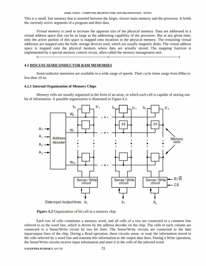
141403, CS2253 – COMPUTER ARCHITECTURE AND ORGANIZATION – NOTES
VASANTHA KUMAR.V AP/CSE 72
This is a small, fast memory that is inserted between the larger, slower main memory and the processor. It holdsthe currently active segments of a program and their data.
Virtual memory is used to increase the apparent size of the physical memory. Data are addressed in avirtual address space that can be as large as the addressing capability of the processor. But at any given time,only the active portion of this space is mapped onto locations in the physical memory. The remaining virtualaddresses are mapped onto the bulk: storage devices used, which are usually magnetic disks. The virtual addressspace is mapped onto the physical memory where data are actually stored. The mapping function isimplemented by a special memory control circuit, often called the memory management unit.
x--------------------------------------------------------x--------------------------------------------------------x
4.2 DISCUSS SEMICONDUCTOR RAM MEMORIES
Semiconductor memories are available in a wide range of speeds. Their cycle times range from l00ns toless than 10 ns.
4.2.1 Internal Organization of Memory Chips
Memory cells are usually organized in the form of an array, in which each cell is capable of storing onebit of information. A possible organization is illustrated in Figure 4.2.
Each row of cells constitutes a memory word, and all cells of a row are connected to a common linereferred to as the word line, which is driven by the address decoder on the chip. The cells in each column areconnected to a Sense/Write circuit by two bit lines. The Sense/Write circuits are connected to the datainput/output lines of the chip. During a Read operation, these circuits sense, or read, the information stored inthe cells selected by a word line and transmit this information to the output data lines. During a Write operation,the Sense/Write circuits receive input information and store it in the cells of the selected word.
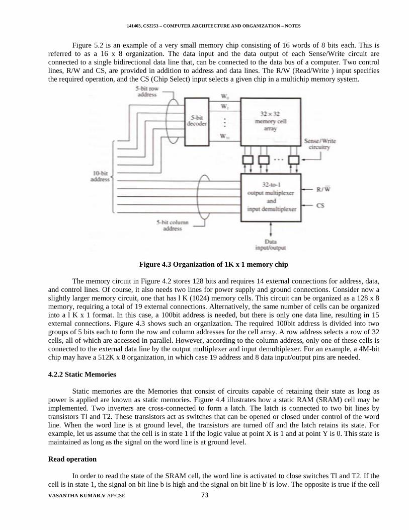
141403, CS2253 – COMPUTER ARCHITECTURE AND ORGANIZATION – NOTES
VASANTHA KUMAR.V AP/CSE 73
Figure 5.2 is an example of a very small memory chip consisting of 16 words of 8 bits each. This isreferred to as a 16 x 8 organization. The data input and the data output of each Sense/Write circuit areconnected to a single bidirectional data line that, can be connected to the data bus of a computer. Two controllines, R/W and CS, are provided in addition to address and data lines. The R/W (Read/Write ) input specifiesthe required operation, and the CS (Chip Select) input selects a given chip in a multichip memory system.
Figure 4.3 Organization of 1K x 1 memory chip
The memory circuit in Figure 4.2 stores 128 bits and requires 14 external connections for address, data,and control lines. Of course, it also needs two lines for power supply and ground connections. Consider now aslightly larger memory circuit, one that has l K (1024) memory cells. This circuit can be organized as a 128 x 8memory, requiring a total of 19 external connections. Alternatively, the same number of cells can be organizedinto a l K x 1 format. In this case, a 100bit address is needed, but there is only one data line, resulting in 15external connections. Figure 4.3 shows such an organization. The required 100bit address is divided into twogroups of 5 bits each to form the row and column addresses for the cell array. A row address selects a row of 32cells, all of which are accessed in parallel. However, according to the column address, only one of these cells isconnected to the external data line by the output multiplexer and input demultiplexer. For an example, a 4M-bitchip may have a 512K x 8 organization, in which case 19 address and 8 data input/output pins are needed.
4.2.2 Static Memories
Static memories are the Memories that consist of circuits capable of retaining their state as long aspower is applied are known as static memories. Figure 4.4 illustrates how a static RAM (SRAM) cell may beimplemented. Two inverters are cross-connected to form a latch. The latch is connected to two bit lines bytransistors Tl and T2. These transistors act as switches that can be opened or closed under control of the wordline. When the word line is at ground level, the transistors are turned off and the latch retains its state. Forexample, let us assume that the cell is in state 1 if the logic value at point X is 1 and at point Y is 0. This state ismaintained as long as the signal on the word line is at ground level.
Read operation
In order to read the state of the SRAM cell, the word line is activated to close switches Tl and T2. If thecell is in state 1, the signal on bit line b is high and the signal on bit line b' is low. The opposite is true if the cell
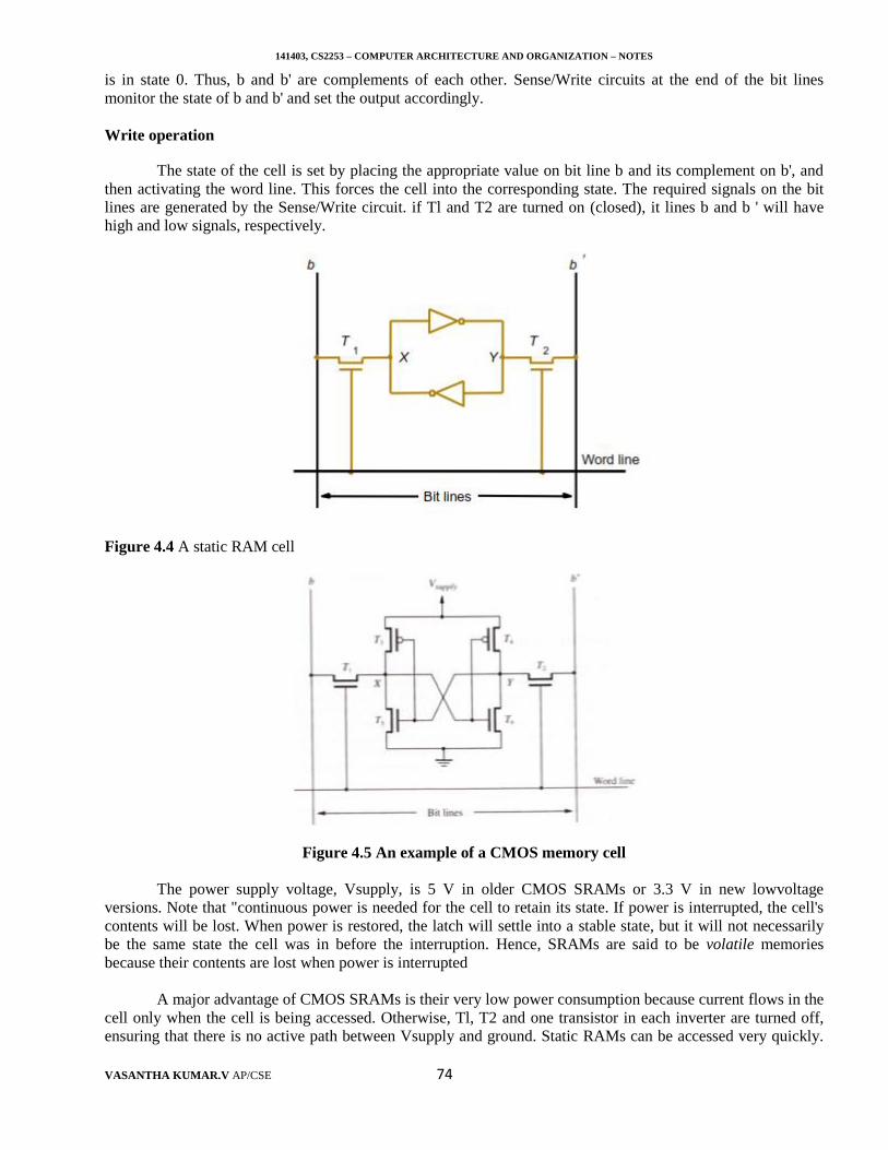
141403, CS2253 – COMPUTER ARCHITECTURE AND ORGANIZATION – NOTES
VASANTHA KUMAR.V AP/CSE 74
is in state 0. Thus, b and b' are complements of each other. Sense/Write circuits at the end of the bit linesmonitor the state of b and b' and set the output accordingly.
Write operation
The state of the cell is set by placing the appropriate value on bit line b and its complement on b', andthen activating the word line. This forces the cell into the corresponding state. The required signals on the bitlines are generated by the Sense/Write circuit. if Tl and T2 are turned on (closed), it lines b and b ' will havehigh and low signals, respectively.
Figure 4.4 A static RAM cell
Figure 4.5 An example of a CMOS memory cell
The power supply voltage, Vsupply, is 5 V in older CMOS SRAMs or 3.3 V in new lowvoltageversions. Note that "continuous power is needed for the cell to retain its state. If power is interrupted, the cell'scontents will be lost. When power is restored, the latch will settle into a stable state, but it will not necessarilybe the same state the cell was in before the interruption. Hence, SRAMs are said to be volatile memoriesbecause their contents are lost when power is interrupted
A major advantage of CMOS SRAMs is their very low power consumption because current flows in thecell only when the cell is being accessed. Otherwise, Tl, T2 and one transistor in each inverter are turned off,ensuring that there is no active path between Vsupply and ground. Static RAMs can be accessed very quickly.
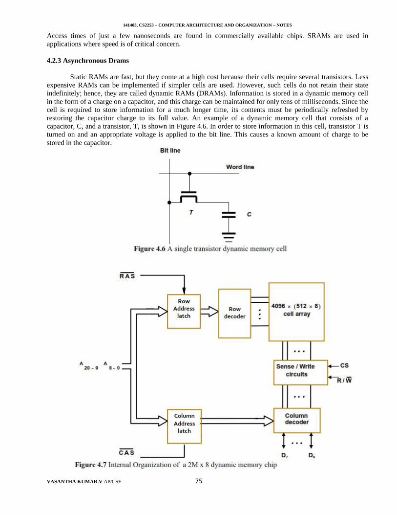
141403, CS2253 – COMPUTER ARCHITECTURE AND ORGANIZATION – NOTES
VASANTHA KUMAR.V AP/CSE 75
Access times of just a few nanoseconds are found in commercially available chips. SRAMs are used inapplications where speed is of critical concern.
4.2.3 Asynchronous Drams
Static RAMs are fast, but they come at a high cost because their cells require several transistors. Lessexpensive RAMs can be implemented if simpler cells are used. However, such cells do not retain their stateindefinitely; hence, they are called dynamic RAMs (DRAMs). Information is stored in a dynamic memory cellin the form of a charge on a capacitor, and this charge can be maintained for only tens of milliseconds. Since thecell is required to store information for a much longer time, its contents must be periodically refreshed byrestoring the capacitor charge to its full value. An example of a dynamic memory cell that consists of acapacitor, C, and a transistor, T, is shown in Figure 4.6. In order to store information in this cell, transistor T isturned on and an appropriate voltage is applied to the bit line. This causes a known amount of charge to bestored in the capacitor.
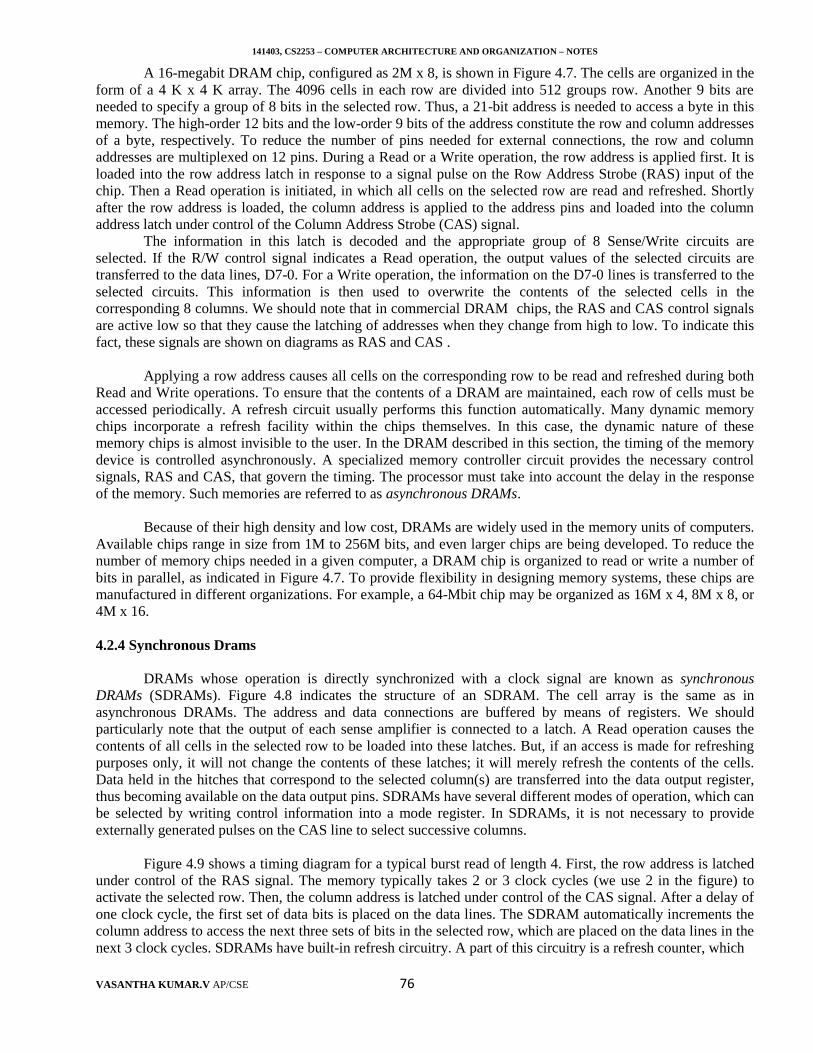
141403, CS2253 – COMPUTER ARCHITECTURE AND ORGANIZATION – NOTES
VASANTHA KUMAR.V AP/CSE 76
A 16-megabit DRAM chip, configured as 2M x 8, is shown in Figure 4.7. The cells are organized in theform of a 4 K x 4 K array. The 4096 cells in each row are divided into 512 groups row. Another 9 bits areneeded to specify a group of 8 bits in the selected row. Thus, a 21-bit address is needed to access a byte in thismemory. The high-order 12 bits and the low-order 9 bits of the address constitute the row and column addressesof a byte, respectively. To reduce the number of pins needed for external connections, the row and columnaddresses are multiplexed on 12 pins. During a Read or a Write operation, the row address is applied first. It isloaded into the row address latch in response to a signal pulse on the Row Address Strobe (RAS) input of thechip. Then a Read operation is initiated, in which all cells on the selected row are read and refreshed. Shortlyafter the row address is loaded, the column address is applied to the address pins and loaded into the columnaddress latch under control of the Column Address Strobe (CAS) signal.
The information in this latch is decoded and the appropriate group of 8 Sense/Write circuits areselected. If the R/W control signal indicates a Read operation, the output values of the selected circuits aretransferred to the data lines, D7-0. For a Write operation, the information on the D7-0 lines is transferred to theselected circuits. This information is then used to overwrite the contents of the selected cells in thecorresponding 8 columns. We should note that in commercial DRAM chips, the RAS and CAS control signalsare active low so that they cause the latching of addresses when they change from high to low. To indicate thisfact, these signals are shown on diagrams as RAS and CAS .
Applying a row address causes all cells on the corresponding row to be read and refreshed during bothRead and Write operations. To ensure that the contents of a DRAM are maintained, each row of cells must beaccessed periodically. A refresh circuit usually performs this function automatically. Many dynamic memorychips incorporate a refresh facility within the chips themselves. In this case, the dynamic nature of thesememory chips is almost invisible to the user. In the DRAM described in this section, the timing of the memorydevice is controlled asynchronously. A specialized memory controller circuit provides the necessary controlsignals, RAS and CAS, that govern the timing. The processor must take into account the delay in the responseof the memory. Such memories are referred to as asynchronous DRAMs.
Because of their high density and low cost, DRAMs are widely used in the memory units of computers.Available chips range in size from 1M to 256M bits, and even larger chips are being developed. To reduce thenumber of memory chips needed in a given computer, a DRAM chip is organized to read or write a number ofbits in parallel, as indicated in Figure 4.7. To provide flexibility in designing memory systems, these chips aremanufactured in different organizations. For example, a 64-Mbit chip may be organized as 16M x 4, 8M x 8, or4M x 16.
4.2.4 Synchronous Drams
DRAMs whose operation is directly synchronized with a clock signal are known as synchronousDRAMs (SDRAMs). Figure 4.8 indicates the structure of an SDRAM. The cell array is the same as inasynchronous DRAMs. The address and data connections are buffered by means of registers. We shouldparticularly note that the output of each sense amplifier is connected to a latch. A Read operation causes thecontents of all cells in the selected row to be loaded into these latches. But, if an access is made for refreshingpurposes only, it will not change the contents of these latches; it will merely refresh the contents of the cells.Data held in the hitches that correspond to the selected column(s) are transferred into the data output register,thus becoming available on the data output pins. SDRAMs have several different modes of operation, which canbe selected by writing control information into a mode register. In SDRAMs, it is not necessary to provideexternally generated pulses on the CAS line to select successive columns.
Figure 4.9 shows a timing diagram for a typical burst read of length 4. First, the row address is latchedunder control of the RAS signal. The memory typically takes 2 or 3 clock cycles (we use 2 in the figure) toactivate the selected row. Then, the column address is latched under control of the CAS signal. After a delay ofone clock cycle, the first set of data bits is placed on the data lines. The SDRAM automatically increments thecolumn address to access the next three sets of bits in the selected row, which are placed on the data lines in thenext 3 clock cycles. SDRAMs have built-in refresh circuitry. A part of this circuitry is a refresh counter, which
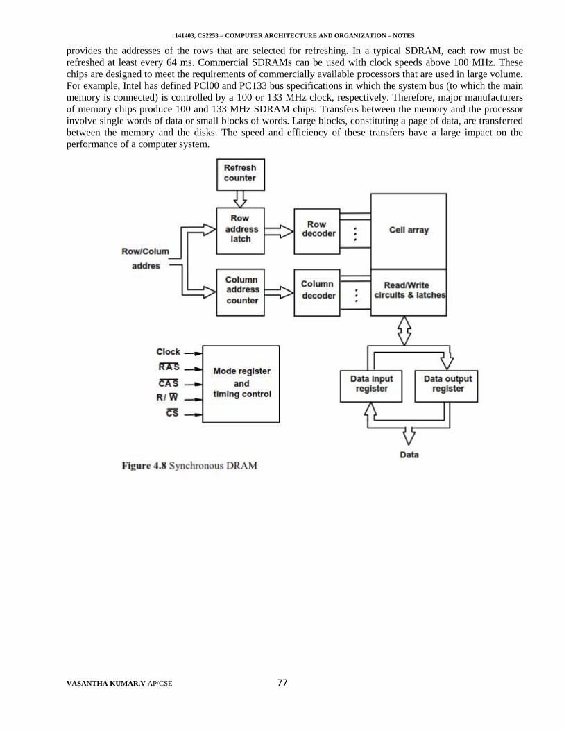
141403, CS2253 – COMPUTER ARCHITECTURE AND ORGANIZATION – NOTES
VASANTHA KUMAR.V AP/CSE 77
provides the addresses of the rows that are selected for refreshing. In a typical SDRAM, each row must berefreshed at least every 64 ms. Commercial SDRAMs can be used with clock speeds above 100 MHz. Thesechips are designed to meet the requirements of commercially available processors that are used in large volume.For example, Intel has defined PCl00 and PC133 bus specifications in which the system bus (to which the mainmemory is connected) is controlled by a 100 or 133 MHz clock, respectively. Therefore, major manufacturersof memory chips produce 100 and 133 MHz SDRAM chips. Transfers between the memory and the processorinvolve single words of data or small blocks of words. Large blocks, constituting a page of data, are transferredbetween the memory and the disks. The speed and efficiency of these transfers have a large impact on theperformance of a computer system.
141403, CS2253 – COMPUTER ARCHITECTURE AND ORGANIZATION – NOTES
VASANTHA KUMAR.V AP/CSE 78
A good indication of the performance is given by two parameters: latency and bandwidth. The termmemory latency is used to refer to the amount of time it takes to transfer a word of data to or from the memory.In the case of reading or writing a single word of data, the latency provides a complete indication of memoryperformance. But, in the case of burst operations that transfer a block of data, the time needed to complete theoperation depends also on the rate at which successive words can be transferred and on the size of the block. Inblock transfers, the term latency is used to denote the time it takes to transfer the first word of data. Whentransferring blocks of data, it is of interest to know how much time is needed to transfer an entire block. Sinceblocks can be variable in size, it is useful to define a performance measure in terms of the number of bits orbytes that can be transferred in one second. This measure is often referred to as the memory bandwidth. Thebandwidth of a memory unit (consisting of one or more memory chips) depends on the speed of access to thestored data and on the number of bits that can be accessed in parallel.
4.2.5 Structure of Larger Memories
Many memory chips are connected to form a much larger memory.
Static Memory System
Consider a memory consisting of 2M (2,097,152) words of 32 bits each. Figure 4.10 shows how we canimplement this memory using 512K x 8 static memory chips. Each column in the figure consists of four chips,which implement one byte position. Four of these sets provide the required 2M x 32 memory. Each chip has acontrol input called Chip Select. When this input is set to 1, it enables the chip to accept data from or to placedata on its data lines. The data output for each chip is of the three-state type. Only the selected chip places dataon the data output line, while all other outputs are in the high-impedance state. Twenty one address bits areneeded to select a 32-bit word in this memory. The high-order 2 bits of the address are decoded to determinewhich of the four Chip Select control signals should be activated and the remaining 19 address bits are used toaccess specific byte locations inside each chip of the selected row. The R/W inputs of all chips are tied togetherto provide a common Rea d/Write control (not shown in the figure).
141403, CS2253 – COMPUTER ARCHITECTURE AND ORGANIZATION – NOTES
VASANTHA KUMAR.V AP/CSE 79
Dynamic Memory System
The organization of large dynamic memory systems is essentially the same as the memory shown inFigure 4.10. However, physical implementation is often done more conveniently in the form of memorymodules. Modem computers use very large memories; even a small personal computer is likely to have at least32M bytes of memory. Typical workstations have at least 128M bytes of memory. A large memory leads tobetter performance because more of the programs and data used in processing can be held in the memory, thusreducing the frequency of accessing the information in secondary storage. However, if a large memory is builtby placing DRAM chips directly on the main system printed-circuit board that contains the processor, oftenreferred to as a motherboard, it will occupy an unacceptably large amount of space on the board. Also, it isawkward to provide for future expansion of the memory, because space must be allocated and wiring providedfor the maximum expected size. These packaging considerations have led to the development of larger memoryunits known as SIMMs (Single In-line Memory Modules) and DIMMs (Dual In-line Memory Modules). Such amodule is an assembly of several Memory chips on a separate small board that plugs vertically into a singlesocket on the motherboard. SIMMs and DIMMs of different sizes are designed to use the same size socket.
4.2.6 Memory System Consideration
There are several factors that determine the choice of a RAM chip for a given application. These factorsare the cost, speed, power dissipation, and size of the chip. Static RAMs are generally used only when very fastoperation is the primary requirement. Their cost and size are adversely affected by the complexity of the circuitthat realizes the basic cell. They are used mostly in cache memories. Dynamic RAMs are the predominantchoice for implementing computer main memories. The high densities achievable in these chips make largememories economically feasible.
141403, CS2253 – COMPUTER ARCHITECTURE AND ORGANIZATION – NOTES
VASANTHA KUMAR.V AP/CSE 80
Memory' Controller
To reduce the number of pins, the dynamic memory chips use multiplexed address inputs. The addressis divided into two parts. The high-order address bits, which select a row in the cell array, are provided first andlatched into the memory chip under control of the RAS signal. Then, the low-order address bits, which select acolumn, are provided on the same address pins and latched using the CAS signal. A typical processor issues allbits of an address at the same time. The required multiplexing of address bits is usually performed by a memorycontroller circuit, which is interposed between the processor and the dynamic memory as shown in Figure 4.11.The controller accepts a complete address and the R/W signal from the processor, under control of a Requestsignal which indicates that a memory access operation is needed. The controller then forwards the row andcolumn portions of the address to the memory and generates the RAS and CAS signals. Thus, the controllerprovides the RAS-CAS timing, in addition to its address multiplexing function. It also sends the R/W and CSsignals to the memory. The CS signal is usually active low; hence it is shown as CS in Figure 4.11. Data linesare connected directly between the processor and the memory. Note that the clock signal is needed in SDRAMchips.
When used with DRAM chips, which do not have self-refreshing capability, the memory controller hasto provide all the information needed to control the refreshing process. It contains a refresh counter thatprovides successive row addresses. Its function is to cause the refreshing of all rows to be done within theperiod specified for a particular device.
Refresh overhead
All dynamic memories have to be refreshed. In older DRAMs, a typical period for refreshing all rowswas 16ms. In typical SDRAMs, a typical period is 64 ms.
x--------------------------------------------------------x--------------------------------------------------------x
4.2.7 RAMBUS MEMORY
A very wide bus is expensive and requires a lot of space on a motherboard. An alternative approach isto implement a narrow bus that is much faster. This approach was used by Rambus Inc. to develop a proprietarydesign known as Rambus. The key feature of Rambus technology is a fast signaling method used to transferinformation between chips. Instead of using signals that have voltage levels of either 0 or Vsupply to representthe logic values, the signals consist of much smaller voltage swings around a reference voltage, Vref. Thereference voltage is about 2 V, and the two logic values are represented by 0.3 V swings above and below Vref.This type of signaling is generally known as differential signaling. Small voltage swings make it possible tohave short transition times, which allows for a high speed of transmission.
141403, CS2253 – COMPUTER ARCHITECTURE AND ORGANIZATION – NOTES
VASANTHA KUMAR.V AP/CSE 81
Rambus requires specially designed memory chips. These chips use cell arrays based on the standardDRAM technology. Multiple banks of cell arrays are used to access more than one word at a time. Circuitryneeded to interface to the Rambus channel is included on the chip. Such chips are known as Rambus DRAMs(RDRAMs). The original specification of Rambus provided for a channel consisting of 9 data lines and anumber of control and power supply lines. Eight of the data lines are intended for transferring a byte of data.The ninth data line can be used for purposes such as parity checking. Subsequent specifications allow foradditional channels. A two-channel Rambus, also known as Direct RDRAM, has 18 data lines intended totransfer two bytes of data at a time. There are no separate address lines.
Communication between the processor, or some other device that can serve as a master, and RDRAMmodules, which serve as slaves, is carried out by means of packets transmitted on the data lines. There are threetypes of packets: request, acknowledge, and data. A request packet issued by the master indicates the type ofoperation that is to be performed. It contains the address of the desired memory location and includes an 8-bitcount that specifies the number of bytes involved in the transfer. The operation types include memory reads andwrites, as well as reading and writing of various control registers in the RDRAM chips. When the master issuesa request packet, the addressed slave responds by returning a positive acknowledgement packet if it canimmediately satisfy the request. Otherwise, the slave indicates that it is "busy" by returning a negativeacknowledgement packet, in which case the master will try again.
The number of bits in a request packet exceeds the number of data lines, which means that several clockcycles are needed to transmit the entire packet. Using a narrow communication link is compensated by the veryhigh rate of transmission. RDRAM chips can be assembled into larger modules, similar to SIMMs and DIMMs.One such module, called RIMM, can hold up to 16 RDRAMs. Rambus technology competes directly with theDDR SDRAM technology. Each has certain advantages and disadvantages. A nontechnical consideration is thatthe specification of DDR SDRAM is an open standard, while RDRAM is a proprietary design of Rambus Inc.for which the manufacturers of chips have to pay a royalty.
x--------------------------------------------------------x--------------------------------------------------------x
4.3 DISCUSS READ ONLY MEMORIES (ROM)
RAM memories are volatile memories, which mean that they lose the stored information if power is turned off.There are many applications that need memory devices which retain the stored information if power is turnedoff. For example, the boot program stored in hard disk must be retained even if power is turned off. A practicalsolution is to provide a small amount of nonvolatile memory that holds the instructions whose execution resultsin loading the boot program from the disk. The contents of such memory can be read as if they were SRAM orDRAM memories. But, a special writing process is needed to place the information into this memory. Since itsnormal operation involves only reading of stored data, a memory of this type is called read-only memory(ROM).
4.3.1 ROM
Figure 4.12 shows a possible configuration for a ROM cell. A logic value 0 is stored in the cell if thetransistor is connected to ground at point P; otherwise, a 1 is stored. The bit line is connected through a resistorto the power supply. To read the state of the cell, the word line is activated. Thus, the transistor switch is closedand the voltage on the bit line drops to near zero if there is a connection between the transistor and ground. Ifthere is no connection to ground, the bit line remains at the high voltage, indicating a 1. A sense circuit at theend of the bit line generates the proper output value. Data are written into a ROM when it is manufactured.
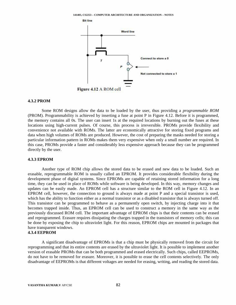
141403, CS2253 – COMPUTER ARCHITECTURE AND ORGANIZATION – NOTES
VASANTHA KUMAR.V AP/CSE 82
4.3.2 PROM
Some ROM designs allow the data to be loaded by the user, thus providing a programmable ROM(PROM). Programmability is achieved by inserting a fuse at point P in Figure 4.12. Before it is programmed,the memory contains all 0s. The user can insert 1s at the required locations by burning out the fuses at theselocations using high-current pulses. Of course, this process is irreversible. PROMs provide flexibility andconvenience not available with ROMs. The latter are economically attractive for storing fixed programs anddata when high volumes of ROMs are produced. However, the cost of preparing the masks needed for storing aparticular information pattern in ROMs makes them very expensive when only a small number are required. Inthis case, PROMs provide a faster and considerably less expensive approach because they can be programmeddirectly by the user.
4.3.3 EPROM
Another type of ROM chip allows the stored data to be erased and new data to be loaded. Such anerasable, reprogrammable ROM is usually called an EPROM. It provides considerable flexibility during thedevelopment phase of digital systems. Since EPROMs are capable of retaining stored information for a longtime, they can be used in place of ROMs while software is being developed. In this way, memory changes andupdates can be easily made. An EPROM cell has a structure similar to the ROM cell in Figure 4.12. In anEPROM cell, however, the connection to ground is always made at point P and a special transistor is used,which has the ability to function either as a normal transistor or as a disabled transistor that is always turned off.This transistor can be programmed to behave as a permanently open switch, by injecting charge into it thatbecomes trapped inside. Thus, an EPROM cell can be used to construct a memory in the same way as thepreviously discussed ROM cell. The important advantage of EPROM chips is that their contents can be erasedand reprogrammed. Erasure requires dissipating the charges trapped in the transistors of memory cells; this canbe done by exposing the chip to ultraviolet light. For this reason, EPROM chips are mounted in packages thathave transparent windows.4.3.4 EEPROM
A significant disadvantage of EPROMs is that a chip must be physically removed from the circuit forreprogramming and that its entire contents are erased by the ultraviolet light. It is possible to implement anotherversion of erasable PROMs that can be both programmed and erased electrically. Such chips, called EEPROMs,do not have to be removed for erasure. Moreover, it is possible to erase the cell contents selectively. The onlydisadvantage of EEPROMs is that different voltages are needed for erasing, writing, and reading the stored data.
141403, CS2253 – COMPUTER ARCHITECTURE AND ORGANIZATION – NOTES
VASANTHA KUMAR.V AP/CSE 83
4.3.5 FLASH MEMORIES
An approach similar to EEPROM technology has more recently given rise to flash memory devices. Aflash cell is based on a single transistor controlled by trapped charge, just like an EEPROM cell. While similarin some respects, there are also substantial differences between flash and EEPROM devices. In EEPROM it ispossible to read and write the contents of a single cell. In a flash device it is possible to read the contents of asingle cell, but it is only possible to write an entire block of cells. Prior to writing, the previous contents of theblock are erased. Flash devices have greater density, which leads to higher capacity and a lower cost per bit.They require a single power supply voltage, and consume less power in their operation. The low powerconsumption of flash memory makes it attractive for use in portable equipment that is battery driven. 1Ypicalapplications include hand-held computers, cell phones, digital cameras, and MP3 music players. Single flashchips do not provide sufficient storage capacity for the applications mentioned above. Larger memory modulesconsisting of a number of chips are needed. There are two popular choices for the implementation of suchmodules: flash cards and flash drives.
Flash Cards
One way of constructing a larger module is to mount flash chips on a small card. Such flash cards havea standard interface that makes them usable in a variety of products. A card is simply plugged into aconveniently accessible slot. Flash cards come in a variety of memory sizes. Typical sizes are 8, 32, 64 MB andso on.
Flash drive
Larger flash memory modules have been developed to replace, hard disk drives. These flash drives aredesigned to fully emulate the bard disks, to the point that they can be fitted into standard disk drive bays. Thefact that flash drives are solid state electronic devices that have no movable parts provides some importantadvantages. They have shorter seek and access times, which results in faster response. They have lower powerconsumption, which makes them attractive for battery driven applications, and they are also insensitive tovibration. Another type of ROM chip allows the stored data to be erased and new data to be loaded. Thedisadvantages of flash drives are less storage capacity, higher cost per bit and it will become weak after it hasbeen written several times.
x--------------------------------------------------------x--------------------------------------------------------x
4.4 DISCUSS SPEED, SIZE AND COST OF MEMORIES
An ideal memory would be fast, large, and inexpensive. a very fast memory can be implemented ifSRAM chips are used. But these chips are expensive because their basic cells have six transistors, whichpreclude packing a very large number of cells onto a single chip. Thus, for cost reasons, it is impractical to builda large memory using SRAM chips. The alternative is to use Dynamic RAM chips, which have much simplerbasic cells and thus are much less expensive. But such memories are significantly slower.
Although dynamic memory units in the range of hundreds of megabytes can be implemented at areasonable cost, the affordable size is still small compared to the demands of large programs with voluminousdata. A solution is provided by using secondary storage, mainly magnetic disks, to implement large memoryspaces. Very large disks are available at a reasonable price, and they are used extensively in computer systems.However, they are much slower than the semiconductor memory units. So a huge amount of cost-effectivestorage can be provided by magnetic disks. A large, yet affordable, main memory can be built with dynamicRAM technology. This leaves SRAMs to be used in smaller units where speed is of the essence, such as incache memories.
141403, CS2253 – COMPUTER ARCHITECTURE AND ORGANIZATION – NOTES
VASANTHA KUMAR.V AP/CSE 84
All of these different types of memory units are employed effectively in a computer. The entirecomputer memory can be viewed as the hierarchy depicted in Figure 4.13. The fastest access is to data held inprocessor registers. Therefore, if we consider the registers to be part of the memory hierarchy, then theprocessor registers are at the top in terms of the speed of access. Of course, the registers provide only aminuscule portion of the required memory.
At the next level of the hierarchy is a relatively small amount of memory that can be implementeddirectly on the processor chip. This memory, called a processor cache, holds copies of instructions and datastored in a much larger memory that is provided externally. There are often two levels of caches. A primarycache is always located on the processor chip. This cache is small because it competes for space on theprocessor chip, which must implement many other functions. The primary cache is referred to as level (L1)cache. A larger, secondary cache is placed between the primary cache and the rest of the memory. It is referredto as level 2 (L2) cache. It is usually implemented using SRAM chips. It is possible to have both Ll and L2caches on the processor chip.
The next level in the hierarchy is called the main memory. This rather large memory is implementedusing dynamic memory components, typically in the form of SIMMs, DIMMs, or RIMMs. The main memory ismuch larger but significantly slower than the cache memory. In a typical computer, the access time for the mainmemory is about ten times longer than the access time for the L 1 cache. Disk devices provide a huge amount ofinexpensive storage. They are very slow compared to the semiconductor devices used to implement the mainmemory.
A hard disk drive (HDD; also hard drive, hard disk, magnetic disk or disk drive) is a device for storingand retrieving digital information, primarily computer data. It consists of one or more rigid (hence "hard")rapidly rotating discs (often referred to as platters), coated with magnetic material and with magnetic headsarranged to write data to the surfaces and read it from them.
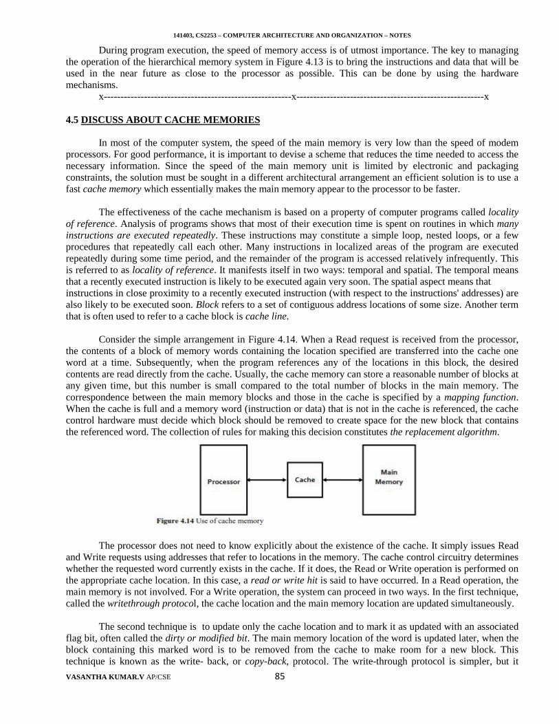
141403, CS2253 – COMPUTER ARCHITECTURE AND ORGANIZATION – NOTES
VASANTHA KUMAR.V AP/CSE 85
During program execution, the speed of memory access is of utmost importance. The key to managingthe operation of the hierarchical memory system in Figure 4.13 is to bring the instructions and data that will beused in the near future as close to the processor as possible. This can be done by using the hardwaremechanisms.
x--------------------------------------------------------x--------------------------------------------------------x
4.5 DISCUSS ABOUT CACHE MEMORIES
In most of the computer system, the speed of the main memory is very low than the speed of modemprocessors. For good performance, it is important to devise a scheme that reduces the time needed to access thenecessary information. Since the speed of the main memory unit is limited by electronic and packagingconstraints, the solution must be sought in a different architectural arrangement an efficient solution is to use afast cache memory which essentially makes the main memory appear to the processor to be faster.
The effectiveness of the cache mechanism is based on a property of computer programs called localityof reference. Analysis of programs shows that most of their execution time is spent on routines in which manyinstructions are executed repeatedly. These instructions may constitute a simple loop, nested loops, or a fewprocedures that repeatedly call each other. Many instructions in localized areas of the program are executedrepeatedly during some time period, and the remainder of the program is accessed relatively infrequently. Thisis referred to as locality of reference. It manifests itself in two ways: temporal and spatial. The temporal meansthat a recently executed instruction is likely to be executed again very soon. The spatial aspect means thatinstructions in close proximity to a recently executed instruction (with respect to the instructions' addresses) arealso likely to be executed soon. Block refers to a set of contiguous address locations of some size. Another termthat is often used to refer to a cache block is cache line.
Consider the simple arrangement in Figure 4.14. When a Read request is received from the processor,the contents of a block of memory words containing the location specified are transferred into the cache oneword at a time. Subsequently, when the program references any of the locations in this block, the desiredcontents are read directly from the cache. Usually, the cache memory can store a reasonable number of blocks atany given time, but this number is small compared to the total number of blocks in the main memory. Thecorrespondence between the main memory blocks and those in the cache is specified by a mapping function.When the cache is full and a memory word (instruction or data) that is not in the cache is referenced, the cachecontrol hardware must decide which block should be removed to create space for the new block that containsthe referenced word. The collection of rules for making this decision constitutes the replacement algorithm.
The processor does not need to know explicitly about the existence of the cache. It simply issues Readand Write requests using addresses that refer to locations in the memory. The cache control circuitry determineswhether the requested word currently exists in the cache. If it does, the Read or Write operation is performed onthe appropriate cache location. In this case, a read or write hit is said to have occurred. In a Read operation, themain memory is not involved. For a Write operation, the system can proceed in two ways. In the first technique,called the writethrough protocol, the cache location and the main memory location are updated simultaneously.
The second technique is to update only the cache location and to mark it as updated with an associatedflag bit, often called the dirty or modified bit. The main memory location of the word is updated later, when theblock containing this marked word is to be removed from the cache to make room for a new block. Thistechnique is known as the write- back, or copy-back, protocol. The write-through protocol is simpler, but it
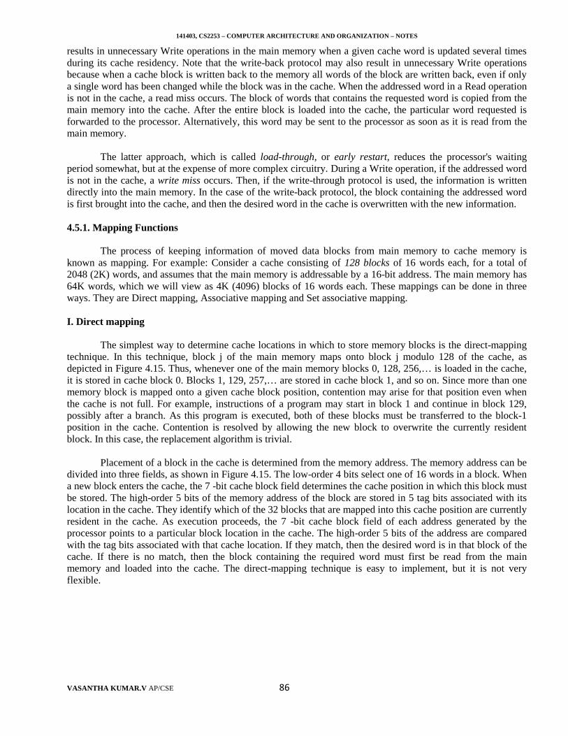
141403, CS2253 – COMPUTER ARCHITECTURE AND ORGANIZATION – NOTES
VASANTHA KUMAR.V AP/CSE 86
results in unnecessary Write operations in the main memory when a given cache word is updated several timesduring its cache residency. Note that the write-back protocol may also result in unnecessary Write operationsbecause when a cache block is written back to the memory all words of the block are written back, even if onlya single word has been changed while the block was in the cache. When the addressed word in a Read operationis not in the cache, a read miss occurs. The block of words that contains the requested word is copied from themain memory into the cache. After the entire block is loaded into the cache, the particular word requested isforwarded to the processor. Alternatively, this word may be sent to the processor as soon as it is read from themain memory.
The latter approach, which is called load-through, or early restart, reduces the processor's waitingperiod somewhat, but at the expense of more complex circuitry. During a Write operation, if the addressed wordis not in the cache, a write miss occurs. Then, if the write-through protocol is used, the information is writtendirectly into the main memory. In the case of the write-back protocol, the block containing the addressed wordis first brought into the cache, and then the desired word in the cache is overwritten with the new information.
4.5.1. Mapping Functions
The process of keeping information of moved data blocks from main memory to cache memory isknown as mapping. For example: Consider a cache consisting of 128 blocks of 16 words each, for a total of2048 (2K) words, and assumes that the main memory is addressable by a 16-bit address. The main memory has64K words, which we will view as 4K (4096) blocks of 16 words each. These mappings can be done in threeways. They are Direct mapping, Associative mapping and Set associative mapping.
I. Direct mapping
The simplest way to determine cache locations in which to store memory blocks is the direct-mappingtechnique. In this technique, block j of the main memory maps onto block j modulo 128 of the cache, asdepicted in Figure 4.15. Thus, whenever one of the main memory blocks 0, 128, 256,… is loaded in the cache,it is stored in cache block 0. Blocks 1, 129, 257,… are stored in cache block 1, and so on. Since more than onememory block is mapped onto a given cache block position, contention may arise for that position even whenthe cache is not full. For example, instructions of a program may start in block 1 and continue in block 129,possibly after a branch. As this program is executed, both of these blocks must be transferred to the block-1position in the cache. Contention is resolved by allowing the new block to overwrite the currently residentblock. In this case, the replacement algorithm is trivial.
Placement of a block in the cache is determined from the memory address. The memory address can bedivided into three fields, as shown in Figure 4.15. The low-order 4 bits select one of 16 words in a block. Whena new block enters the cache, the 7 -bit cache block field determines the cache position in which this block mustbe stored. The high-order 5 bits of the memory address of the block are stored in 5 tag bits associated with itslocation in the cache. They identify which of the 32 blocks that are mapped into this cache position are currentlyresident in the cache. As execution proceeds, the 7 -bit cache block field of each address generated by theprocessor points to a particular block location in the cache. The high-order 5 bits of the address are comparedwith the tag bits associated with that cache location. If they match, then the desired word is in that block of thecache. If there is no match, then the block containing the required word must first be read from the mainmemory and loaded into the cache. The direct-mapping technique is easy to implement, but it is not veryflexible.
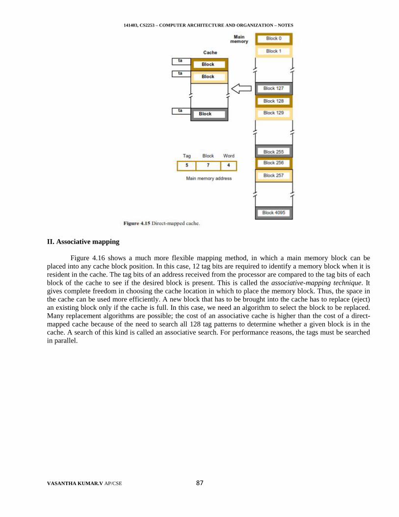
141403, CS2253 – COMPUTER ARCHITECTURE AND ORGANIZATION – NOTES
VASANTHA KUMAR.V AP/CSE 87
II. Associative mapping
Figure 4.16 shows a much more flexible mapping method, in which a main memory block can beplaced into any cache block position. In this case, 12 tag bits are required to identify a memory block when it isresident in the cache. The tag bits of an address received from the processor are compared to the tag bits of eachblock of the cache to see if the desired block is present. This is called the associative-mapping technique. Itgives complete freedom in choosing the cache location in which to place the memory block. Thus, the space inthe cache can be used more efficiently. A new block that has to be brought into the cache has to replace (eject)an existing block only if the cache is full. In this case, we need an algorithm to select the block to be replaced.Many replacement algorithms are possible; the cost of an associative cache is higher than the cost of a direct-mapped cache because of the need to search all 128 tag patterns to determine whether a given block is in thecache. A search of this kind is called an associative search. For performance reasons, the tags must be searchedin parallel.
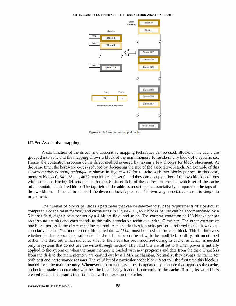
141403, CS2253 – COMPUTER ARCHITECTURE AND ORGANIZATION – NOTES
VASANTHA KUMAR.V AP/CSE 88
III. Set-Associative mapping
A combination of the direct- and associative-mapping techniques can be used. Blocks of the cache aregrouped into sets, and the mapping allows a block of the main memory to reside in any block of a specific set.Hence, the contention problem of the direct method is eased by having a few choices for block placement. Atthe same time, the hardware cost is reduced by decreasing the size of the associative search. An example of thisset-associative-mapping technique is shown in Figure 4.17 for a cache with two blocks per set. In this case,memory blocks 0, 64, 128, …, 4032 map into cache set 0, and they can occupy either of the two block positionswithin this set. Having 64 sets means that the 6-bit set field of the address determines which set of the cachemight contain the desired block. The tag field of the address must then be associatively compared to the tags ofthe two blocks of the set to check if the desired block is present. This two-way associative search is simple toimplement.
The number of blocks per set is a parameter that can be selected to suit the requirements of a particularcomputer. For the main memory and cache sizes in Figure 4.17, four blocks per set can be accommodated by a5-bit set field, eight blocks per set by a 4-bit set field, and so on. The extreme condition of 128 blocks per setrequires no set bits and corresponds to the fully associative technique, with 12 tag bits. The other extreme ofone block per set is the direct-mapping method. A cache that has k blocks per set is referred to as a k-way set-associative cache. One more control bit, called the valid bit, must be provided for each block. This bit indicateswhether the block contains valid data. It should not be confused with the modified, or dirty, bit mentionedearlier. The dirty bit, which indicates whether the block has been modified during its cache residency, is neededonly in systems that do not use the write-through method. The valid bits are all set to 0 when power is initiallyapplied to the system or when the main memory is loaded with new programs and data from the disk. Transfersfrom the disk to the main memory are carried out by a DMA mechanism. Normally, they bypass the cache forboth cost and performance reasons. The valid bit of a particular cache block is set to 1 the first time this block isloaded from the main memory. Whenever a main memory block is updated by a source that bypasses the cache,a check is made to determine whether the block being loaded is currently in the cache. If it is, its valid bit iscleared to O. This ensures that stale data will not exist in the cache.
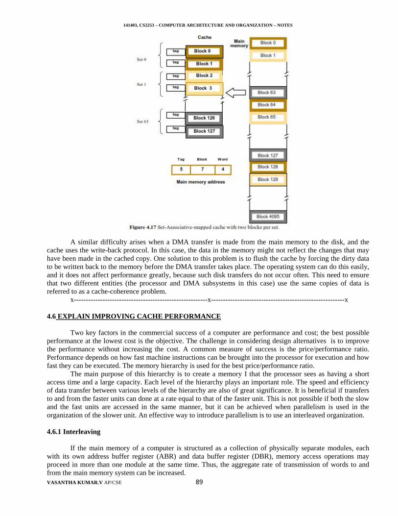
141403, CS2253 – COMPUTER ARCHITECTURE AND ORGANIZATION – NOTES
VASANTHA KUMAR.V AP/CSE 89
A similar difficulty arises when a DMA transfer is made from the main memory to the disk, and thecache uses the write-back protocol. In this case, the data in the memory might not reflect the changes that mayhave been made in the cached copy. One solution to this problem is to flush the cache by forcing the dirty datato be written back to the memory before the DMA transfer takes place. The operating system can do this easily,and it does not affect performance greatly, because such disk transfers do not occur often. This need to ensurethat two different entities (the processor and DMA subsystems in this case) use the same copies of data isreferred to as a cache-coherence problem.
x--------------------------------------------------------x--------------------------------------------------------x
4.6 EXPLAIN IMPROVING CACHE PERFORMANCE
Two key factors in the commercial success of a computer are performance and cost; the best possibleperformance at the lowest cost is the objective. The challenge in considering design alternatives is to improvethe performance without increasing the cost. A common measure of success is the price/performance ratio.Performance depends on how fast machine instructions can be brought into the processor for execution and howfast they can be executed. The memory hierarchy is used for the best price/performance ratio.
The main purpose of this hierarchy is to create a memory I that the processor sees as having a shortaccess time and a large capacity. Each level of the hierarchy plays an important role. The speed and efficiencyof data transfer between various levels of the hierarchy are also of great significance. It is beneficial if transfersto and from the faster units can done at a rate equal to that of the faster unit. This is not possible if both the slowand the fast units are accessed in the same manner, but it can be achieved when parallelism is used in theorganization of the slower unit. An effective way to introduce parallelism is to use an interleaved organization.
4.6.1 Interleaving
If the main memory of a computer is structured as a collection of physically separate modules, eachwith its own address buffer register (ABR) and data buffer register (DBR), memory access operations mayproceed in more than one module at the same time. Thus, the aggregate rate of transmission of words to andfrom the main memory system can be increased.
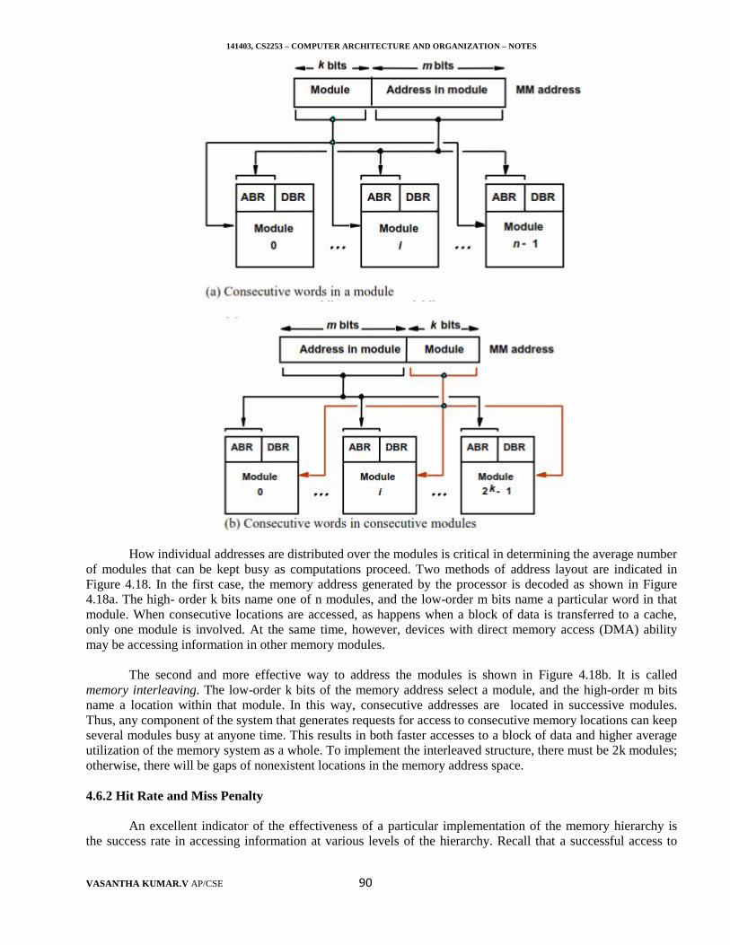
141403, CS2253 – COMPUTER ARCHITECTURE AND ORGANIZATION – NOTES
VASANTHA KUMAR.V AP/CSE 90
How individual addresses are distributed over the modules is critical in determining the average numberof modules that can be kept busy as computations proceed. Two methods of address layout are indicated inFigure 4.18. In the first case, the memory address generated by the processor is decoded as shown in Figure4.18a. The high- order k bits name one of n modules, and the low-order m bits name a particular word in thatmodule. When consecutive locations are accessed, as happens when a block of data is transferred to a cache,only one module is involved. At the same time, however, devices with direct memory access (DMA) abilitymay be accessing information in other memory modules.
The second and more effective way to address the modules is shown in Figure 4.18b. It is calledmemory interleaving. The low-order k bits of the memory address select a module, and the high-order m bitsname a location within that module. In this way, consecutive addresses are located in successive modules.Thus, any component of the system that generates requests for access to consecutive memory locations can keepseveral modules busy at anyone time. This results in both faster accesses to a block of data and higher averageutilization of the memory system as a whole. To implement the interleaved structure, there must be 2k modules;otherwise, there will be gaps of nonexistent locations in the memory address space.
4.6.2 Hit Rate and Miss Penalty
An excellent indicator of the effectiveness of a particular implementation of the memory hierarchy isthe success rate in accessing information at various levels of the hierarchy. Recall that a successful access to
141403, CS2253 – COMPUTER ARCHITECTURE AND ORGANIZATION – NOTES
VASANTHA KUMAR.V AP/CSE 91
data in a cache is called a hit. The number of hits stated as a fraction of all attempted accesses is called the hitrate, and the miss rate is the number of misses stated as a fraction of attempted accesses.
Ideally, the entire memory hierarchy would appear to the processor as a single memory unit that has theaccess time of a cache on the processor chip and the size of a magnetic disk. How close we get to this idealdepends largely on the hit rate at different levels of the hierarchy. High hit rates, well over 0.9, are essential forhigh-performance computers. Performance is adversely affected by the actions that must be taken after a miss.The extra time needed to bring the desired information into the cache is called the miss penalty. This penaltyis ultimately reflected in the time that the processor is stalled because the required instructions or data are notavailable for execution. In general, the miss penalty is the time needed to bring a block of data from a slowerunit in the memory hierarchy to a faster unit. The miss penalty is reduced if efficient mechanisms fortransferring data between the various units of the hierarchy are implemented. The previous section shows howan interleaved memory can reduce the miss penalty substantially.
4.6.3 Caches on the Processor Chip
From the speed point of view, the optimal place for a cache is on the processor chip. Unfortunately,space on the processor chip is needed for many other functions; this limits the size of the cache that can beaccommodated. All high-performance processor chips include some form of a cache. Some manufacturershave chosen to implement two separate caches, one for instructions and another for data. A combined cache forinstructions and data is likely to have a somewhat better hit rate because it offers greater flexibility in mappingnew information into the cache. However, if separate caches are used, it is possible to access both caches at thesame time, which leads to increased parallelism and, hence, better performance.
The disadvantage of separate caches is that the increased parallelism comes at the expense of morecomplex circuitry (more cost). In high-performance processors two levels of caches are normally used. The L1cache( s) is on the processor chip. The L2 cache, which is much larger, may be implemented externally usingSRAM chips. But, a somewhat smaller L2 cache may also be implemented on the processor chip. If both L1 andL2 caches are used, the L1 cache should be designed to allow very fast access by the processor because itsaccess time will have a large effect on the clock rate of the processor. A cache cannot be accessed at the samespeed as a register file because the cache is much bigger and, hence, more complex. A practical way to speed upaccess to the cache is to access more than one word simultaneously and then let the processor use them one at atime.
The L2 cache can be slower, but it should be much larger to ensure a high hit rate. Its speed is lesscritical because it only affects the miss penalty of the L 1 cache. A workstation computer may include an Llcache with the capacity of tens of kilobytes and an L2 cache of several megabytes. Including an L2 cachefurther reduces the impact of the main memory speed on the performance of a computer. The average accesstime experienced by the processor in a system with two levels of caches is
tave = h1 C1 + (1 - h1) h2 C2 + ( 1 - h1 ) ( 1 - h2 ) M
Whereh1 is the hit rate in the Ll cache.h2 is the hit rate in the L2 cache.C1 is the time to access information in the Ll cache.C2 is the time to access information in the L2 cache.M is the time to access information in the main memory.
The number of misses in the L2 cache, given by the term ( 1 - h1 ) ( 1 - h2 ), should be low. If both h1and h 2 are in the 90 percent range, then the number of misses will be less than 1 percent of the processor'smemory accesses. Thus, the miss penalty M will be less critical from a performance point of view.
141403, CS2253 – COMPUTER ARCHITECTURE AND ORGANIZATION – NOTES
VASANTHA KUMAR.V AP/CSE 92
4.6.4 OTHER ENHANCEMENTS
In addition to the main design issues just discussed, several other possibilities exist for enhancingperformance. They are
Write Buffer
When the write-through protocol is used, each write operation results in writing a new value into themain memory. If the processor must wait for the memory function to be completed, as we have assumed untilnow, then the processor is slowed down by all write requests. Yet the processor typically does not immediatelydepend on the result of a write operation, so it is not necessary for the processor to wait for the write request tobe completed. To improve performance, a write buffer can be included for temporary storage of write requests.The processor places each write request into this buffer and continues execution of the next instruction. Thewrite requests stored in the write buffer are sent to the main memory whenever the memory is not responding toread requests. Note that it is important that the read requests be serviced immediately because the processorusually cannot proceed without the data that are to be read from the memory. Hence, these requests are givenpriority over write requests.
Write-back protocol
A different situation occurs with the write-back protocol. In this case, the write operations are simply performedon the corresponding word in the cache. But consider what happens when a new block of data is to be broughtinto the cache as a result of a read miss, which replaces an existing block that has some dirty data. The dirtyblock has to be written into the main memory. If the required write-back is performed first, then the processorwill have to wait longer for the new block to be read into the cache. It is more prudent to read the new blockfirst. This can be arranged by providing a fast write buffer for temporary storage of the dirty block that isejected from the cache while the new block is being read. Afterward, the contents of the buffer are written intothe main memory. Thus, the write buffer also works well for the write-back protocol.
Prefetching
In the cache mechanism, new data are brought into the cache when they are first needed. A read miss occurs,and the desired data are loaded from the main memory. The processor has to pause until the new data arrive,which is the effect of the miss penalty.To avoid stalling the processor, it is possible to prefetch the data into thecache before they are needed. The simplest way to do this is through software. A special prefetch instructionmay be provided in the instruction set of the processor. Executing this instruction causes the addressed data tobe loaded into the cache, as in the case of a read miss. However, the processor does not wait for the referenceddata. A prefetch instruction is inserted in a program to cause the data to be loaded in the cache by the time theyare needed in the program. The hope is that prefetching will take place while the processor is busy executinginstructions that do not result in a read miss, thus allowing accesses to the main memory to be overlapped withcomputation in the processor.
Prefetch instructions can be inserted into a program either by the programmer or by the compiler. Theoverall effect of software prefetching on performance is positive, and many processors have machineinstructions to support this feature. Prefetching can also be done through hardware. This involves addingcircuitry that attempts to discover a pattern in memory references and then prefetches data according to thispattern.
Lockup-Free cache
The software prefetching scheme just discussed does not work well if it interferes significantly with the normalexecution of instructions. This is the case if the action of prefetching stops other accesses to the cache until theprefetch is completed. A cache of this type is said to be locked while it services a miss. This problem can be
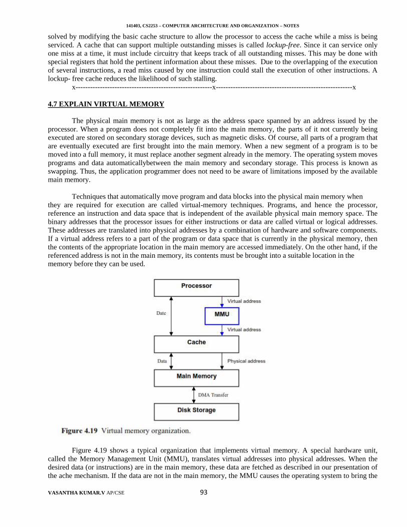
141403, CS2253 – COMPUTER ARCHITECTURE AND ORGANIZATION – NOTES
VASANTHA KUMAR.V AP/CSE 93
solved by modifying the basic cache structure to allow the processor to access the cache while a miss is beingserviced. A cache that can support multiple outstanding misses is called lockup-free. Since it can service onlyone miss at a time, it must include circuitry that keeps track of all outstanding misses. This may be done withspecial registers that hold the pertinent information about these misses. Due to the overlapping of the executionof several instructions, a read miss caused by one instruction could stall the execution of other instructions. Alockup- free cache reduces the likelihood of such stalling.
x--------------------------------------------------------x--------------------------------------------------------x
4.7 EXPLAIN VIRTUAL MEMORY
The physical main memory is not as large as the address space spanned by an address issued by theprocessor. When a program does not completely fit into the main memory, the parts of it not currently beingexecuted are stored on secondary storage devices, such as magnetic disks. Of course, all parts of a program thatare eventually executed are first brought into the main memory. When a new segment of a program is to bemoved into a full memory, it must replace another segment already in the memory. The operating system movesprograms and data automaticallybetween the main memory and secondary storage. This process is known asswapping. Thus, the application programmer does not need to be aware of limitations imposed by the availablemain memory.
Techniques that automatically move program and data blocks into the physical main memory whenthey are required for execution are called virtual-memory techniques. Programs, and hence the processor,reference an instruction and data space that is independent of the available physical main memory space. Thebinary addresses that the processor issues for either instructions or data are called virtual or logical addresses.These addresses are translated into physical addresses by a combination of hardware and software components.If a virtual address refers to a part of the program or data space that is currently in the physical memory, thenthe contents of the appropriate location in the main memory are accessed immediately. On the other hand, if thereferenced address is not in the main memory, its contents must be brought into a suitable location in thememory before they can be used.
Figure 4.19 shows a typical organization that implements virtual memory. A special hardware unit,called the Memory Management Unit (MMU), translates virtual addresses into physical addresses. When thedesired data (or instructions) are in the main memory, these data are fetched as described in our presentation ofthe ache mechanism. If the data are not in the main memory, the MMU causes the operating system to bring the
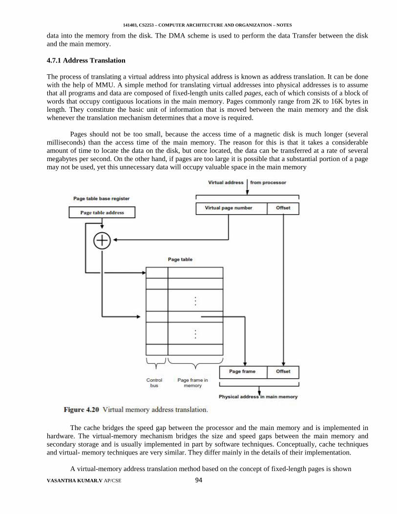
141403, CS2253 – COMPUTER ARCHITECTURE AND ORGANIZATION – NOTES
VASANTHA KUMAR.V AP/CSE 94
data into the memory from the disk. The DMA scheme is used to perform the data Transfer between the diskand the main memory.
4.7.1 Address Translation
The process of translating a virtual address into physical address is known as address translation. It can be donewith the help of MMU. A simple method for translating virtual addresses into physical addresses is to assumethat all programs and data are composed of fixed-length units called pages, each of which consists of a block ofwords that occupy contiguous locations in the main memory. Pages commonly range from 2K to 16K bytes inlength. They constitute the basic unit of information that is moved between the main memory and the diskwhenever the translation mechanism determines that a move is required.
Pages should not be too small, because the access time of a magnetic disk is much longer (severalmilliseconds) than the access time of the main memory. The reason for this is that it takes a considerableamount of time to locate the data on the disk, but once located, the data can be transferred at a rate of severalmegabytes per second. On the other hand, if pages are too large it is possible that a substantial portion of a pagemay not be used, yet this unnecessary data will occupy valuable space in the main memory
The cache bridges the speed gap between the processor and the main memory and is implemented inhardware. The virtual-memory mechanism bridges the size and speed gaps between the main memory andsecondary storage and is usually implemented in part by software techniques. Conceptually, cache techniquesand virtual- memory techniques are very similar. They differ mainly in the details of their implementation.
A virtual-memory address translation method based on the concept of fixed-length pages is shown
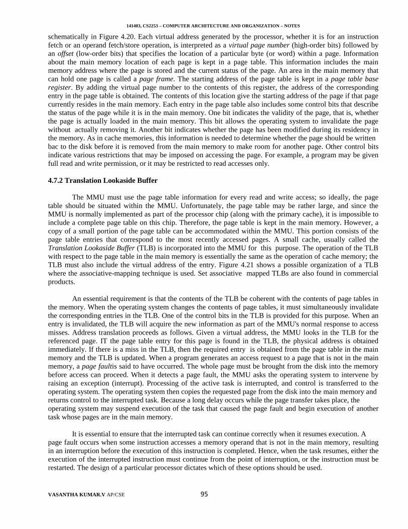
141403, CS2253 – COMPUTER ARCHITECTURE AND ORGANIZATION – NOTES
VASANTHA KUMAR.V AP/CSE 95
schematically in Figure 4.20. Each virtual address generated by the processor, whether it is for an instructionfetch or an operand fetch/store operation, is interpreted as a virtual page number (high-order bits) followed byan offset (low-order bits) that specifies the location of a particular byte (or word) within a page. Informationabout the main memory location of each page is kept in a page table. This information includes the mainmemory address where the page is stored and the current status of the page. An area in the main memory thatcan hold one page is called a page frame. The starting address of the page table is kept in a page table baseregister. By adding the virtual page number to the contents of this register, the address of the correspondingentry in the page table is obtained. The contents of this location give the starting address of the page if that pagecurrently resides in the main memory. Each entry in the page table also includes some control bits that describethe status of the page while it is in the main memory. One bit indicates the validity of the page, that is, whetherthe page is actually loaded in the main memory. This bit allows the operating system to invalidate the pagewithout actually removing it. Another bit indicates whether the page has been modified during its residency inthe memory. As in cache memories, this information is needed to determine whether the page should be writtenbac to the disk before it is removed from the main memory to make room for another page. Other control bitsindicate various restrictions that may be imposed on accessing the page. For example, a program may be givenfull read and write permission, or it may be restricted to read accesses only.
4.7.2 Translation Lookaside Buffer
The MMU must use the page table information for every read and write access; so ideally, the pagetable should be situated within the MMU. Unfortunately, the page table may be rather large, and since theMMU is normally implemented as part of the processor chip (along with the primary cache), it is impossible toinclude a complete page table on this chip. Therefore, the page table is kept in the main memory. However, acopy of a small portion of the page table can be accommodated within the MMU. This portion consists of thepage table entries that correspond to the most recently accessed pages. A small cache, usually called theTranslation Lookaside Buffer (TLB) is incorporated into the MMU for this purpose. The operation of the TLBwith respect to the page table in the main memory is essentially the same as the operation of cache memory; theTLB must also include the virtual address of the entry. Figure 4.21 shows a possible organization of a TLBwhere the associative-mapping technique is used. Set associative mapped TLBs are also found in commercialproducts.
An essential requirement is that the contents of the TLB be coherent with the contents of page tables inthe memory. When the operating system changes the contents of page tables, it must simultaneously invalidatethe corresponding entries in the TLB. One of the control bits in the TLB is provided for this purpose. When anentry is invalidated, the TLB will acquire the new information as part of the MMU's normal response to accessmisses. Address translation proceeds as follows. Given a virtual address, the MMU looks in the TLB for thereferenced page. IT the page table entry for this page is found in the TLB, the physical address is obtainedimmediately. If there is a miss in the TLB, then the required entry is obtained from the page table in the mainmemory and the TLB is updated. When a program generates an access request to a page that is not in the mainmemory, a page faultis said to have occurred. The whole page must be brought from the disk into the memorybefore access can proceed. When it detects a page fault, the MMU asks the operating system to intervene byraising an exception (interrupt). Processing of the active task is interrupted, and control is transferred to theoperating system. The operating system then copies the requested page from the disk into the main memory andreturns control to the interrupted task. Because a long delay occurs while the page transfer takes place, theoperating system may suspend execution of the task that caused the page fault and begin execution of anothertask whose pages are in the main memory.
It is essential to ensure that the interrupted task can continue correctly when it resumes execution. Apage fault occurs when some instruction accesses a memory operand that is not in the main memory, resultingin an interruption before the execution of this instruction is completed. Hence, when the task resumes, either theexecution of the interrupted instruction must continue from the point of interruption, or the instruction must berestarted. The design of a particular processor dictates which of these options should be used.
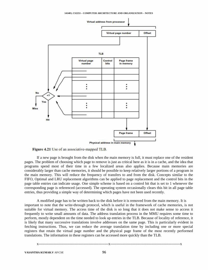
141403, CS2253 – COMPUTER ARCHITECTURE AND ORGANIZATION – NOTES
VASANTHA KUMAR.V AP/CSE 96
If a new page is brought from the disk when the main memory is full, it must replace one of the residentpages. The problem of choosing which page to remove is just as critical here as it is in a cache, and the idea thatprograms spend most of their time in a few localized areas also applies. Because main memories areconsiderably larger than cache memories, it should be possible to keep relatively larger portions of a program inthe main memory. This will reduce the frequency of transfers to and from the disk. Concepts similar to theFIFO, Optimal and LRU replacement algorithms can be applied to page replacement and the control bits in thepage table entries can indicate usage. One simple scheme is based on a control bit that is set to 1 whenever thecorresponding page is referenced (accessed). The operating system occasionally clears this bit in all page tableentries, thus providing a simple way of determining which pages have not been used recently.
A modified page has to be written back to the disk before it is removed from the main memory. It isimportant to note that the write-through protocol, which is useful in the framework of cache memories, is notsuitable for virtual memory. The access time of the disk is so long that it does not make sense to access itfrequently to write small amounts of data. The address translation process in the MMU requires some time toperform, mostly dependent on the time needed to look up entries in the TLB. Because of locality of reference, itis likely that many successive translations involve addresses on the same page. This is particularly evident infetching instructions. Thus, we can reduce the average translation time by including one or more specialregisters that retain the virtual page number and the physical page frame of the most recently performedtranslations. The information in these registers can be accessed more quickly than the TLB.
x--------------------------------------------------------x--------------------------------------------------------x
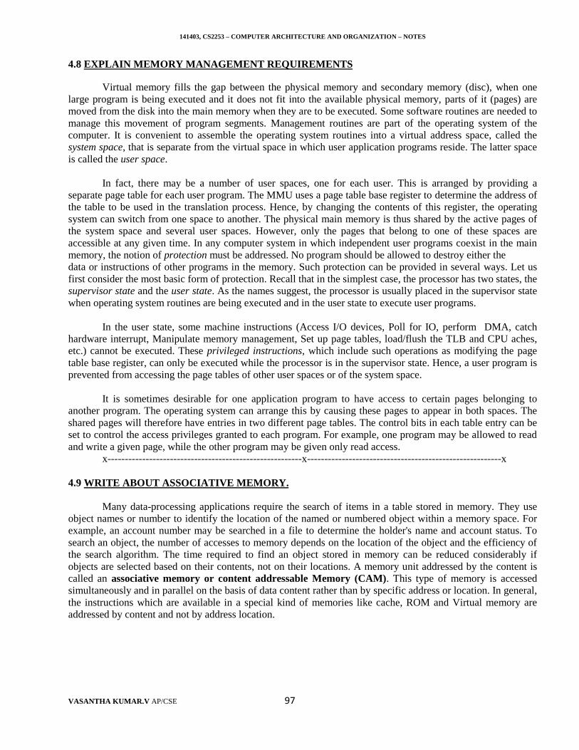
141403, CS2253 – COMPUTER ARCHITECTURE AND ORGANIZATION – NOTES
VASANTHA KUMAR.V AP/CSE 97
4.8 EXPLAIN MEMORY MANAGEMENT REQUIREMENTS
Virtual memory fills the gap between the physical memory and secondary memory (disc), when onelarge program is being executed and it does not fit into the available physical memory, parts of it (pages) aremoved from the disk into the main memory when they are to be executed. Some software routines are needed tomanage this movement of program segments. Management routines are part of the operating system of thecomputer. It is convenient to assemble the operating system routines into a virtual address space, called thesystem space, that is separate from the virtual space in which user application programs reside. The latter spaceis called the user space.
In fact, there may be a number of user spaces, one for each user. This is arranged by providing aseparate page table for each user program. The MMU uses a page table base register to determine the address ofthe table to be used in the translation process. Hence, by changing the contents of this register, the operatingsystem can switch from one space to another. The physical main memory is thus shared by the active pages ofthe system space and several user spaces. However, only the pages that belong to one of these spaces areaccessible at any given time. In any computer system in which independent user programs coexist in the mainmemory, the notion of protection must be addressed. No program should be allowed to destroy either thedata or instructions of other programs in the memory. Such protection can be provided in several ways. Let usfirst consider the most basic form of protection. Recall that in the simplest case, the processor has two states, thesupervisor state and the user state. As the names suggest, the processor is usually placed in the supervisor statewhen operating system routines are being executed and in the user state to execute user programs.
In the user state, some machine instructions (Access I/O devices, Poll for IO, perform DMA, catchhardware interrupt, Manipulate memory management, Set up page tables, load/flush the TLB and CPU aches,etc.) cannot be executed. These privileged instructions, which include such operations as modifying the pagetable base register, can only be executed while the processor is in the supervisor state. Hence, a user program isprevented from accessing the page tables of other user spaces or of the system space.
It is sometimes desirable for one application program to have access to certain pages belonging toanother program. The operating system can arrange this by causing these pages to appear in both spaces. Theshared pages will therefore have entries in two different page tables. The control bits in each table entry can beset to control the access privileges granted to each program. For example, one program may be allowed to readand write a given page, while the other program may be given only read access.
x--------------------------------------------------------x--------------------------------------------------------x
4.9 WRITE ABOUT ASSOCIATIVE MEMORY.
Many data-processing applications require the search of items in a table stored in memory. They useobject names or number to identify the location of the named or numbered object within a memory space. Forexample, an account number may be searched in a file to determine the holder's name and account status. Tosearch an object, the number of accesses to memory depends on the location of the object and the efficiency ofthe search algorithm. The time required to find an object stored in memory can be reduced considerably ifobjects are selected based on their contents, not on their locations. A memory unit addressed by the content iscalled an associative memory or content addressable Memory (CAM). This type of memory is accessedsimultaneously and in parallel on the basis of data content rather than by specific address or location. In general,the instructions which are available in a special kind of memories like cache, ROM and Virtual memory areaddressed by content and not by address location.
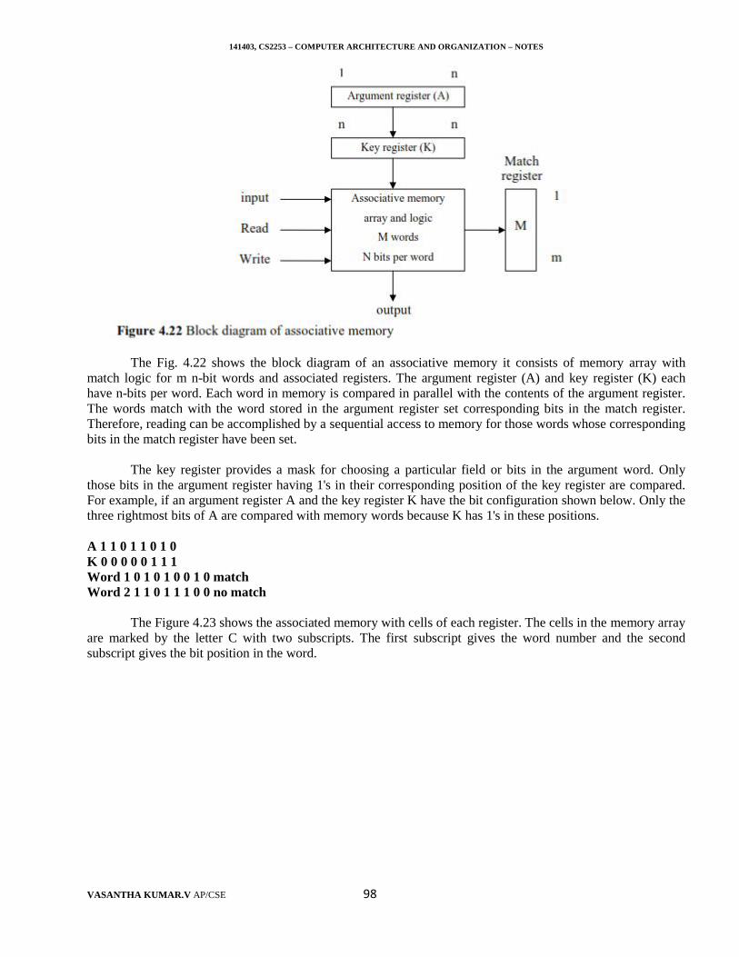
141403, CS2253 – COMPUTER ARCHITECTURE AND ORGANIZATION – NOTES
VASANTHA KUMAR.V AP/CSE 98
The Fig. 4.22 shows the block diagram of an associative memory it consists of memory array withmatch logic for m n-bit words and associated registers. The argument register (A) and key register (K) eachhave n-bits per word. Each word in memory is compared in parallel with the contents of the argument register.The words match with the word stored in the argument register set corresponding bits in the match register.Therefore, reading can be accomplished by a sequential access to memory for those words whose correspondingbits in the match register have been set.
The key register provides a mask for choosing a particular field or bits in the argument word. Onlythose bits in the argument register having 1's in their corresponding position of the key register are compared.For example, if an argument register A and the key register K have the bit configuration shown below. Only thethree rightmost bits of A are compared with memory words because K has 1's in these positions.
A 1 1 0 1 1 0 1 0K 0 0 0 0 0 1 1 1Word 1 0 1 0 1 0 0 1 0 matchWord 2 1 1 0 1 1 1 0 0 no match
The Figure 4.23 shows the associated memory with cells of each register. The cells in the memory arrayare marked by the letter C with two subscripts. The first subscript gives the word number and the secondsubscript gives the bit position in the word.
141403, CS2253 – COMPUTER ARCHITECTURE AND ORGANIZATION – NOTES
VASANTHA KUMAR.V AP/CSE 99
Read Operation
In the read operation, all matched words are read in sequence by applying a read signal to each wordline whose corresponding Mi bit is logic 1. In applications where no two identical items are stored in thememory, only one word may match the unmasked argument field. In such case, we can use Mi output directlyas a read signal for the corresponding word. The contents of the matched word will be presented automaticallyat the output lines and no special read signal is needed.
Write Operation
In write operation, consider two separate cases: 1. It is necessary to load entire memory with newinformation. 2. It is necessary to replace one word with new information. The entire memory can be loaded withnew information by addressing each location in sequence. This will make the memory device a random accessmemory for writing and a content addressable memory for reading. Here, the address for the input can bedecoded as in a random access memory. Thus instead of having m address lines, one for each word, the numberof address lines can be reduced by the use of decoder to d lines, where m = 2d .
To implement the write operation in the second case the tag register is used. This register has as manybits as there are words in the memory for every active (valid) word stored in the memory. The corresponding bitin the tag register is set to 1. When word is deleted from the memory the corresponding tag bit is cleared, i.e. itis set to logic 0. The word is then stored in the memory by scanning the tag register until the first 0 bit isencountered. This gives the first available inactive word and a position for writing a new word. After the newword is stored in the memory it is made active by setting the corresponding tag bit in the tag register.
x--------------------------------------------------------x--------------------------------------------------------x
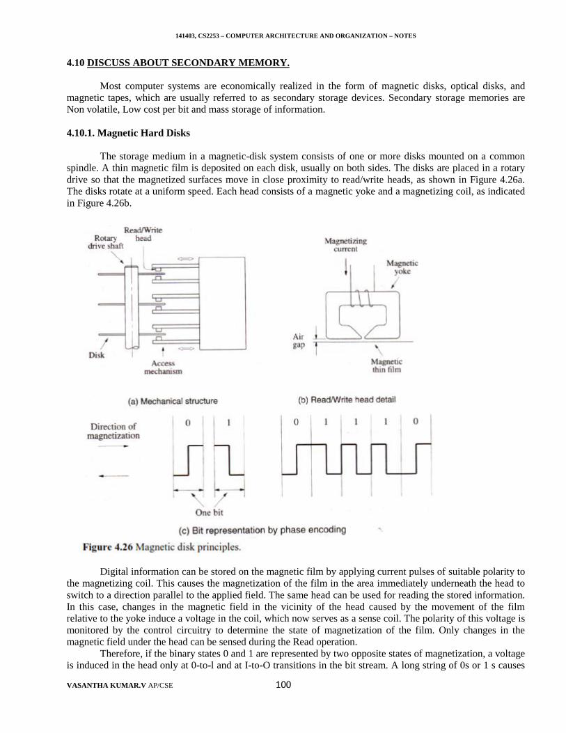
141403, CS2253 – COMPUTER ARCHITECTURE AND ORGANIZATION – NOTES
VASANTHA KUMAR.V AP/CSE 100
4.10 DISCUSS ABOUT SECONDARY MEMORY.
Most computer systems are economically realized in the form of magnetic disks, optical disks, andmagnetic tapes, which are usually referred to as secondary storage devices. Secondary storage memories areNon volatile, Low cost per bit and mass storage of information.
4.10.1. Magnetic Hard Disks
The storage medium in a magnetic-disk system consists of one or more disks mounted on a commonspindle. A thin magnetic film is deposited on each disk, usually on both sides. The disks are placed in a rotarydrive so that the magnetized surfaces move in close proximity to read/write heads, as shown in Figure 4.26a.The disks rotate at a uniform speed. Each head consists of a magnetic yoke and a magnetizing coil, as indicatedin Figure 4.26b.
Digital information can be stored on the magnetic film by applying current pulses of suitable polarity tothe magnetizing coil. This causes the magnetization of the film in the area immediately underneath the head toswitch to a direction parallel to the applied field. The same head can be used for reading the stored information.In this case, changes in the magnetic field in the vicinity of the head caused by the movement of the filmrelative to the yoke induce a voltage in the coil, which now serves as a sense coil. The polarity of this voltage ismonitored by the control circuitry to determine the state of magnetization of the film. Only changes in themagnetic field under the head can be sensed during the Read operation.
Therefore, if the binary states 0 and 1 are represented by two opposite states of magnetization, a voltageis induced in the head only at 0-to-l and at I-to-O transitions in the bit stream. A long string of 0s or 1 s causes
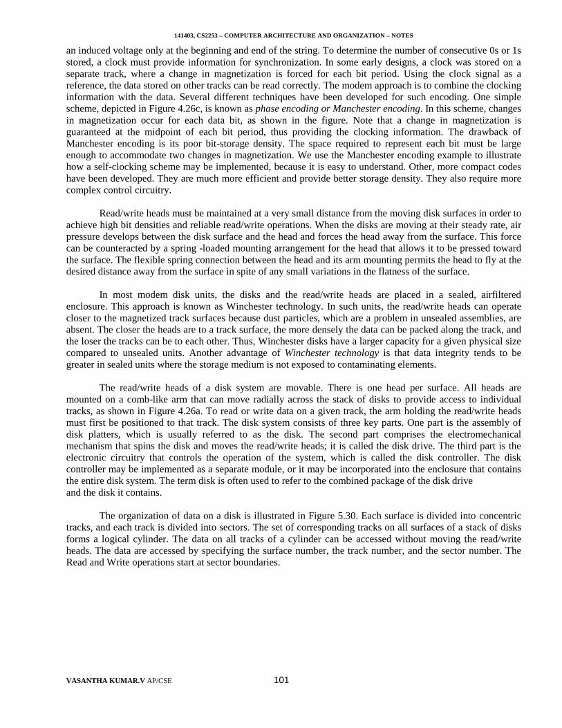
141403, CS2253 – COMPUTER ARCHITECTURE AND ORGANIZATION – NOTES
VASANTHA KUMAR.V AP/CSE 101
an induced voltage only at the beginning and end of the string. To determine the number of consecutive 0s or 1sstored, a clock must provide information for synchronization. In some early designs, a clock was stored on aseparate track, where a change in magnetization is forced for each bit period. Using the clock signal as areference, the data stored on other tracks can be read correctly. The modem approach is to combine the clockinginformation with the data. Several different techniques have been developed for such encoding. One simplescheme, depicted in Figure 4.26c, is known as phase encoding or Manchester encoding. In this scheme, changesin magnetization occur for each data bit, as shown in the figure. Note that a change in magnetization isguaranteed at the midpoint of each bit period, thus providing the clocking information. The drawback ofManchester encoding is its poor bit-storage density. The space required to represent each bit must be largeenough to accommodate two changes in magnetization. We use the Manchester encoding example to illustratehow a self-clocking scheme may be implemented, because it is easy to understand. Other, more compact codeshave been developed. They are much more efficient and provide better storage density. They also require morecomplex control circuitry.
Read/write heads must be maintained at a very small distance from the moving disk surfaces in order toachieve high bit densities and reliable read/write operations. When the disks are moving at their steady rate, airpressure develops between the disk surface and the head and forces the head away from the surface. This forcecan be counteracted by a spring -loaded mounting arrangement for the head that allows it to be pressed towardthe surface. The flexible spring connection between the head and its arm mounting permits the head to fly at thedesired distance away from the surface in spite of any small variations in the flatness of the surface.
In most modem disk units, the disks and the read/write heads are placed in a sealed, airfilteredenclosure. This approach is known as Winchester technology. In such units, the read/write heads can operatecloser to the magnetized track surfaces because dust particles, which are a problem in unsealed assemblies, areabsent. The closer the heads are to a track surface, the more densely the data can be packed along the track, andthe loser the tracks can be to each other. Thus, Winchester disks have a larger capacity for a given physical sizecompared to unsealed units. Another advantage of Winchester technology is that data integrity tends to begreater in sealed units where the storage medium is not exposed to contaminating elements.
The read/write heads of a disk system are movable. There is one head per surface. All heads aremounted on a comb-like arm that can move radially across the stack of disks to provide access to individualtracks, as shown in Figure 4.26a. To read or write data on a given track, the arm holding the read/write headsmust first be positioned to that track. The disk system consists of three key parts. One part is the assembly ofdisk platters, which is usually referred to as the disk. The second part comprises the electromechanicalmechanism that spins the disk and moves the read/write heads; it is called the disk drive. The third part is theelectronic circuitry that controls the operation of the system, which is called the disk controller. The diskcontroller may be implemented as a separate module, or it may be incorporated into the enclosure that containsthe entire disk system. The term disk is often used to refer to the combined package of the disk driveand the disk it contains.
The organization of data on a disk is illustrated in Figure 5.30. Each surface is divided into concentrictracks, and each track is divided into sectors. The set of corresponding tracks on all surfaces of a stack of disksforms a logical cylinder. The data on all tracks of a cylinder can be accessed without moving the read/writeheads. The data are accessed by specifying the surface number, the track number, and the sector number. TheRead and Write operations start at sector boundaries.
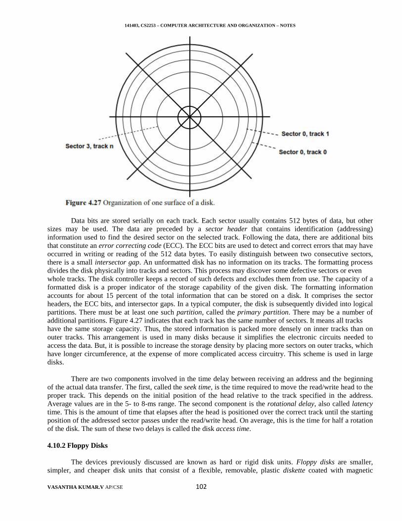
141403, CS2253 – COMPUTER ARCHITECTURE AND ORGANIZATION – NOTES
VASANTHA KUMAR.V AP/CSE 102
Data bits are stored serially on each track. Each sector usually contains 512 bytes of data, but othersizes may be used. The data are preceded by a sector header that contains identification (addressing)information used to find the desired sector on the selected track. Following the data, there are additional bitsthat constitute an error correcting code (ECC). The ECC bits are used to detect and correct errors that may haveoccurred in writing or reading of the 512 data bytes. To easily distinguish between two consecutive sectors,there is a small intersector gap. An unformatted disk has no information on its tracks. The formatting processdivides the disk physically into tracks and sectors. This process may discover some defective sectors or evenwhole tracks. The disk controller keeps a record of such defects and excludes them from use. The capacity of aformatted disk is a proper indicator of the storage capability of the given disk. The formatting informationaccounts for about 15 percent of the total information that can be stored on a disk. It comprises the sectorheaders, the ECC bits, and intersector gaps. In a typical computer, the disk is subsequently divided into logicalpartitions. There must be at least one such partition, called the primary partition. There may be a number ofadditional partitions. Figure 4.27 indicates that each track has the same number of sectors. It means all trackshave the same storage capacity. Thus, the stored information is packed more densely on inner tracks than onouter tracks. This arrangement is used in many disks because it simplifies the electronic circuits needed toaccess the data. But, it is possible to increase the storage density by placing more sectors on outer tracks, whichhave longer circumference, at the expense of more complicated access circuitry. This scheme is used in largedisks.
There are two components involved in the time delay between receiving an address and the beginningof the actual data transfer. The first, called the seek time, is the time required to move the read/write head to theproper track. This depends on the initial position of the head relative to the track specified in the address.Average values are in the 5- to 8-ms range. The second component is the rotational delay, also called latencytime. This is the amount of time that elapses after the head is positioned over the correct track until the startingposition of the addressed sector passes under the read/write head. On average, this is the time for half a rotationof the disk. The sum of these two delays is called the disk access time.
4.10.2 Floppy Disks
The devices previously discussed are known as hard or rigid disk units. Floppy disks are smaller,simpler, and cheaper disk units that consist of a flexible, removable, plastic diskette coated with magnetic
141403, CS2253 – COMPUTER ARCHITECTURE AND ORGANIZATION – NOTES
VASANTHA KUMAR.V AP/CSE 103
material. The diskette is enclosed in a plastic jacket, which has an opening where the read/write head makescontact with the diskette. A hole in the center of the diskette allows a spindle mechanism in the disk drive toposition and rotate the diskette.
One of the simplest schemes used in the first floppy disks for recording data is phase or Manchesterencoding mentioned earlier. Disks encoded in this way are said to have single density. A more complicatedvariant of this scheme, called double density, is most often used in current standard floppy disks. It increases thestorage density by a factor of 2 but also requires more complex circuits in the disk controller. The main featureof floppy disks is their low cost and shipping convenience. However, they have much smaller storagecapacities, longer access times, and higher failure rates than hard disks. Current standard floppy disks are 3.25inches in diameter and store 1.44 or 2 Mbytes of data. Larger super-floppy disks are also available. One type ofsuch disks, known as the zip disk, can store more than 100 Mbytes. In recent years, the attraction of floppy-disktechnology has been diminished by the emergence of rewritable compact disks.
4.10.3 Raid Disk Array
A storage system based on multiple disks are called it RAID, for Redundant Array of InexpensiveDisks. Using multiple disks also makes it possible to improve the reliability of the overall system. Six differentconfigurations were proposed. They are known as RAID levels even though there is no hierarchy involved.RAID 0 is the basic configuration intended to enhance performance. A single large file is stored in severalseparate disk units by breaking the file up into a number of smaller pieces and storing these pieces on differentdisks. This is called data striping. When the file is accessed for a read, all disks can deliver their data in parallel.RAID 1 is intended to provide better reliability by storing identical copies of data on two disks rather than justone. The two disks are said to be mirrors of each other. Then, if one disk drive fails, all read and writeoperations are directed to its mirror drive. This is a costly way to improve the reliability because all disks areduplicated. RAID 2, RAID 3, and RAID 4 levels achieve increased reliability through various parity checkingschemes without requiring a full duplication of disks. All of the parity information is kept on one disk. RAID 5also makes use of a parity-based error-recovery scheme. However, the parity information is distributed amongall disks, rather than being stored on one disk.
4.10.4 Optical Disks
Large storage devices can also be implemented using optical means. The familiar compact disk (CD),used in audio systems, was the first practical application of this technology. Soon after, the optical technologywas adapted to the computer environment to provide high-capacity readonly storage referred to as CD-ROM.The first generation of CDs was developed in the mid-1980s by the Sony and Philips companies, which alsopublished a complete specification for these devices.
CD Technology
The optical technology that is used for CD systems is based on a laser light source. A laser beam isdirected onto the surface of the spinning disk. Physical indentations in the surface are arranged along the tracksof the disk. They reflect the focused beam toward a photo detector, which detects the stored binary patterns.The laser emits a coherent light beam that is sharply focused on the surface of the disk.
Coherent light consists of synchronized waves that have the same wavelength. If a coherent light beamis combined with another beam of the same kind, and the two beams are in phase, then the result will be abrighter beam. But, if the waves of the two beams are 180 degrees out of phase, they will cancel each other.Thus, if a photo detector is used to detect the beams, it will detect a bright spot in the first case and a dark spotin the second case.
A cross-section of a small portion of a CD is shown in Figure 4.30a. The bottom layer is polycarbonateplastic, which functions as a clear glass base. The surface of this plastic is programmed to store data byindenting it with pits. The unintended parts are called lands. A thin layer of reflecting aluminum material isplaced on top of a programmed disk. The aluminum is then covered by a protective acrylic. Finally, the topmost
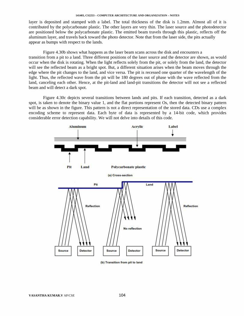
141403, CS2253 – COMPUTER ARCHITECTURE AND ORGANIZATION – NOTES
VASANTHA KUMAR.V AP/CSE 104
layer is deposited and stamped with a label. The total thickness of the disk is 1.2mm. Almost all of it iscontributed by the polycarbonate plastic. The other layers are very thin. The laser source and the photodetectorare positioned below the polycarbonate plastic. The emitted beam travels through this plastic, reflects off thealuminum layer, and travels back toward the photo detector. Note that from the laser side, the pits actuallyappear as bumps with respect to the lands.
Figure 4.30b shows what happens as the laser beam scans across the disk and encounters atransition from a pit to a land. Three different positions of the laser source and the detector are shown, as wouldoccur when the disk is rotating. When the light reflects solely from the pit, or solely from the land, the detectorwill see the reflected beam as a bright spot. But, a different situation arises when the beam moves through theedge where the pit changes to the land, and vice versa. The pit is recessed one quarter of the wavelength of thelight. Thus, the reflected wave from the pit will be 180 degrees out of phase with the wave reflected from theland, canceling each other. Hence, at the pit-land and land-pit transitions the detector will not see a reflectedbeam and will detect a dark spot.
Figure 4.30c depicts several transitions between lands and pits. If each transition, detected as a darkspot, is taken to denote the binary value 1, and the flat portions represent Os, then the detected binary patternwill be as shown in the figure. This pattern is not a direct representation of the stored data. CDs use a complexencoding scheme to represent data. Each byte of data is represented by a 14-bit code, which providesconsiderable error detection capability. We will not delve into details of this code.
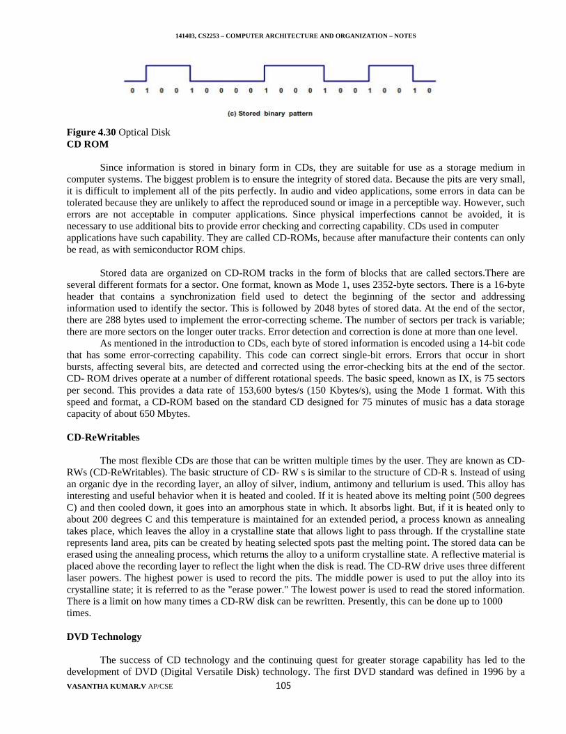
141403, CS2253 – COMPUTER ARCHITECTURE AND ORGANIZATION – NOTES
VASANTHA KUMAR.V AP/CSE 105
Figure 4.30 Optical DiskCD ROM
Since information is stored in binary form in CDs, they are suitable for use as a storage medium incomputer systems. The biggest problem is to ensure the integrity of stored data. Because the pits are very small,it is difficult to implement all of the pits perfectly. In audio and video applications, some errors in data can betolerated because they are unlikely to affect the reproduced sound or image in a perceptible way. However, sucherrors are not acceptable in computer applications. Since physical imperfections cannot be avoided, it isnecessary to use additional bits to provide error checking and correcting capability. CDs used in computerapplications have such capability. They are called CD-ROMs, because after manufacture their contents can onlybe read, as with semiconductor ROM chips.
Stored data are organized on CD-ROM tracks in the form of blocks that are called sectors.There areseveral different formats for a sector. One format, known as Mode 1, uses 2352-byte sectors. There is a 16-byteheader that contains a synchronization field used to detect the beginning of the sector and addressinginformation used to identify the sector. This is followed by 2048 bytes of stored data. At the end of the sector,there are 288 bytes used to implement the error-correcting scheme. The number of sectors per track is variable;there are more sectors on the longer outer tracks. Error detection and correction is done at more than one level.
As mentioned in the introduction to CDs, each byte of stored information is encoded using a 14-bit codethat has some error-correcting capability. This code can correct single-bit errors. Errors that occur in shortbursts, affecting several bits, are detected and corrected using the error-checking bits at the end of the sector.CD- ROM drives operate at a number of different rotational speeds. The basic speed, known as IX, is 75 sectorsper second. This provides a data rate of 153,600 bytes/s (150 Kbytes/s), using the Mode 1 format. With thisspeed and format, a CD-ROM based on the standard CD designed for 75 minutes of music has a data storagecapacity of about 650 Mbytes.
CD-ReWritables
The most flexible CDs are those that can be written multiple times by the user. They are known as CD-RWs (CD-ReWritables). The basic structure of CD- RW s is similar to the structure of CD-R s. Instead of usingan organic dye in the recording layer, an alloy of silver, indium, antimony and tellurium is used. This alloy hasinteresting and useful behavior when it is heated and cooled. If it is heated above its melting point (500 degreesC) and then cooled down, it goes into an amorphous state in which. It absorbs light. But, if it is heated only toabout 200 degrees C and this temperature is maintained for an extended period, a process known as annealingtakes place, which leaves the alloy in a crystalline state that allows light to pass through. If the crystalline staterepresents land area, pits can be created by heating selected spots past the melting point. The stored data can beerased using the annealing process, which returns the alloy to a uniform crystalline state. A reflective material isplaced above the recording layer to reflect the light when the disk is read. The CD-RW drive uses three differentlaser powers. The highest power is used to record the pits. The middle power is used to put the alloy into itscrystalline state; it is referred to as the "erase power." The lowest power is used to read the stored information.There is a limit on how many times a CD-RW disk can be rewritten. Presently, this can be done up to 1000times.
DVD Technology
The success of CD technology and the continuing quest for greater storage capability has led to thedevelopment of DVD (Digital Versatile Disk) technology. The first DVD standard was defined in 1996 by a
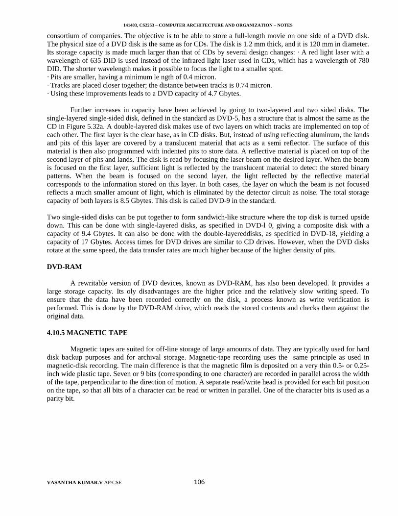
141403, CS2253 – COMPUTER ARCHITECTURE AND ORGANIZATION – NOTES
VASANTHA KUMAR.V AP/CSE 106
consortium of companies. The objective is to be able to store a full-length movie on one side of a DVD disk.The physical size of a DVD disk is the same as for CDs. The disk is 1.2 mm thick, and it is 120 mm in diameter.Its storage capacity is made much larger than that of CDs by several design changes: · A red light laser with awavelength of 635 DID is used instead of the infrared light laser used in CDs, which has a wavelength of 780DID. The shorter wavelength makes it possible to focus the light to a smaller spot.· Pits are smaller, having a minimum le ngth of 0.4 micron.· Tracks are placed closer together; the distance between tracks is 0.74 micron.· Using these improvements leads to a DVD capacity of 4.7 Gbytes.
Further increases in capacity have been achieved by going to two-layered and two sided disks. Thesingle-layered single-sided disk, defined in the standard as DVD-5, has a structure that is almost the same as theCD in Figure 5.32a. A double-layered disk makes use of two layers on which tracks are implemented on top ofeach other. The first layer is the clear base, as in CD disks. But, instead of using reflecting aluminum, the landsand pits of this layer are covered by a translucent material that acts as a semi reflector. The surface of thismaterial is then also programmed with indented pits to store data. A reflective material is placed on top of thesecond layer of pits and lands. The disk is read by focusing the laser beam on the desired layer. When the beamis focused on the first layer, sufficient light is reflected by the translucent material to detect the stored binarypatterns. When the beam is focused on the second layer, the light reflected by the reflective materialcorresponds to the information stored on this layer. In both cases, the layer on which the beam is not focusedreflects a much smaller amount of light, which is eliminated by the detector circuit as noise. The total storagecapacity of both layers is 8.5 Gbytes. This disk is called DVD-9 in the standard.
Two single-sided disks can be put together to form sandwich-like structure where the top disk is turned upsidedown. This can be done with single-layered disks, as specified in DVD-l 0, giving a composite disk with acapacity of 9.4 Gbytes. It can also be done with the double-layereddisks, as specified in DVD-18, yielding acapacity of 17 Gbytes. Access times for DVD drives are similar to CD drives. However, when the DVD disksrotate at the same speed, the data transfer rates are much higher because of the higher density of pits.
DVD-RAM
A rewritable version of DVD devices, known as DVD-RAM, has also been developed. It provides alarge storage capacity. Its oly disadvantages are the higher price and the relatively slow writing speed. Toensure that the data have been recorded correctly on the disk, a process known as write verification isperformed. This is done by the DVD-RAM drive, which reads the stored contents and checks them against theoriginal data.
4.10.5 MAGNETIC TAPE
Magnetic tapes are suited for off-line storage of large amounts of data. They are typically used for harddisk backup purposes and for archival storage. Magnetic-tape recording uses the same principle as used inmagnetic-disk recording. The main difference is that the magnetic film is deposited on a very thin 0.5- or 0.25-inch wide plastic tape. Seven or 9 bits (corresponding to one character) are recorded in parallel across the widthof the tape, perpendicular to the direction of motion. A separate read/write head is provided for each bit positionon the tape, so that all bits of a character can be read or written in parallel. One of the character bits is used as aparity bit.
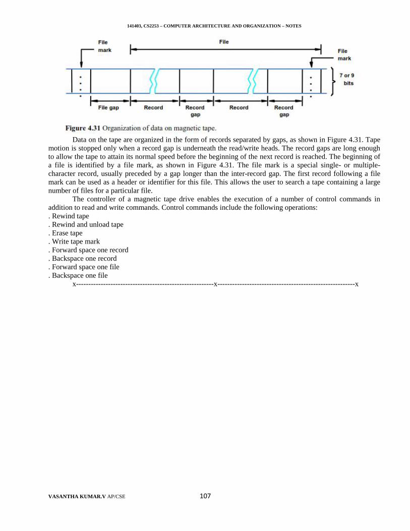
141403, CS2253 – COMPUTER ARCHITECTURE AND ORGANIZATION – NOTES
VASANTHA KUMAR.V AP/CSE 107
Data on the tape are organized in the form of records separated by gaps, as shown in Figure 4.31. Tapemotion is stopped only when a record gap is underneath the read/write heads. The record gaps are long enoughto allow the tape to attain its normal speed before the beginning of the next record is reached. The beginning ofa file is identified by a file mark, as shown in Figure 4.31. The file mark is a special single- or multiple-character record, usually preceded by a gap longer than the inter-record gap. The first record following a filemark can be used as a header or identifier for this file. This allows the user to search a tape containing a largenumber of files for a particular file.
The controller of a magnetic tape drive enables the execution of a number of control commands inaddition to read and write commands. Control commands include the following operations:. Rewind tape. Rewind and unload tape. Erase tape. Write tape mark. Forward space one record. Backspace one record. Forward space one file. Backspace one file
x--------------------------------------------------------x--------------------------------------------------------x
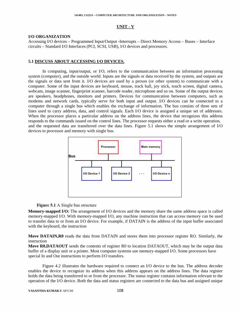
141403, CS2253 – COMPUTER ARCHITECTURE AND ORGANIZATION – NOTES
VASANTHA KUMAR.V AP/CSE 108
UNIT - V
I/O ORGANIZATIONAccessing I/O devices – Programmed Input/Output -Interrupts – Direct Memory Access – Buses – Interfacecircuits – Standard I/O Interfaces (PCI, SCSI, USB), I/O devices and processors.
5.1 DISCUSS ABOUT ACCESSING I/O DEVICES.
In computing, input/output, or I/O, refers to the communication between an information processingsystem (computer), and the outside world. Inputs are the signals or data received by the system, and outputs arethe signals or data sent from it. I/O devices are used by a person (or other system) to communicate with acomputer. Some of the input devices are keyboard, mouse, track ball, joy stick, touch screen, digital camera,webcam, image scanner, fingerprint scanner, barcode reader, microphone and so on. Some of the output devicesare speakers, headphones, monitors and printers. Devices for communication between computers, such asmodems and network cards, typically serve for both input and output. I/O devices can be connected to acomputer through a single bus which enables the exchange of information. The bus consists of three sets oflines used to carry address, data, and control signals. Each I/O device is assigned a unique set of addresses.When the processor places a particular address on the address lines, the device that recognizes this addressresponds to the commands issued on the control lines. The processor requests either a read or a write operation,and the requested data are transferred over the data lines. Figure 5.1 shows the simple arrangement of I/Odevices to processor and memory with single bus.
Memory-mapped I/O: The arrangement of I/O devices and the memory share the same address space is calledmemory-mapped I/O. With memory-mapped I/O, any machine instruction that can access memory can be usedto transfer data to or from an I/O device. For example, if DATAIN is the address of the input buffer associatedwith the keyboard, the instruction
Move DATAIN,R0 reads the data from DATAIN and stores them into processor register RO. Similarly, theinstructionMove R0,DATAOUT sends the contents of register R0 to location DATAOUT, which may be the output databuffer of a display unit or a printer. Most computer systems use memory-mapped I/O. Some processors havespecial In and Out instructions to perform I/O transfers.
Figure 4.2 illustrates the hardware required to connect an I/O device to the bus. The address decoderenables the device to recognize its address when this address appears on the address lines. The data registerholds the data being transferred to or from the processor. The status register contains information relevant to theoperation of the I/O device. Both the data and status registers are connected to the data bus and assigned unique
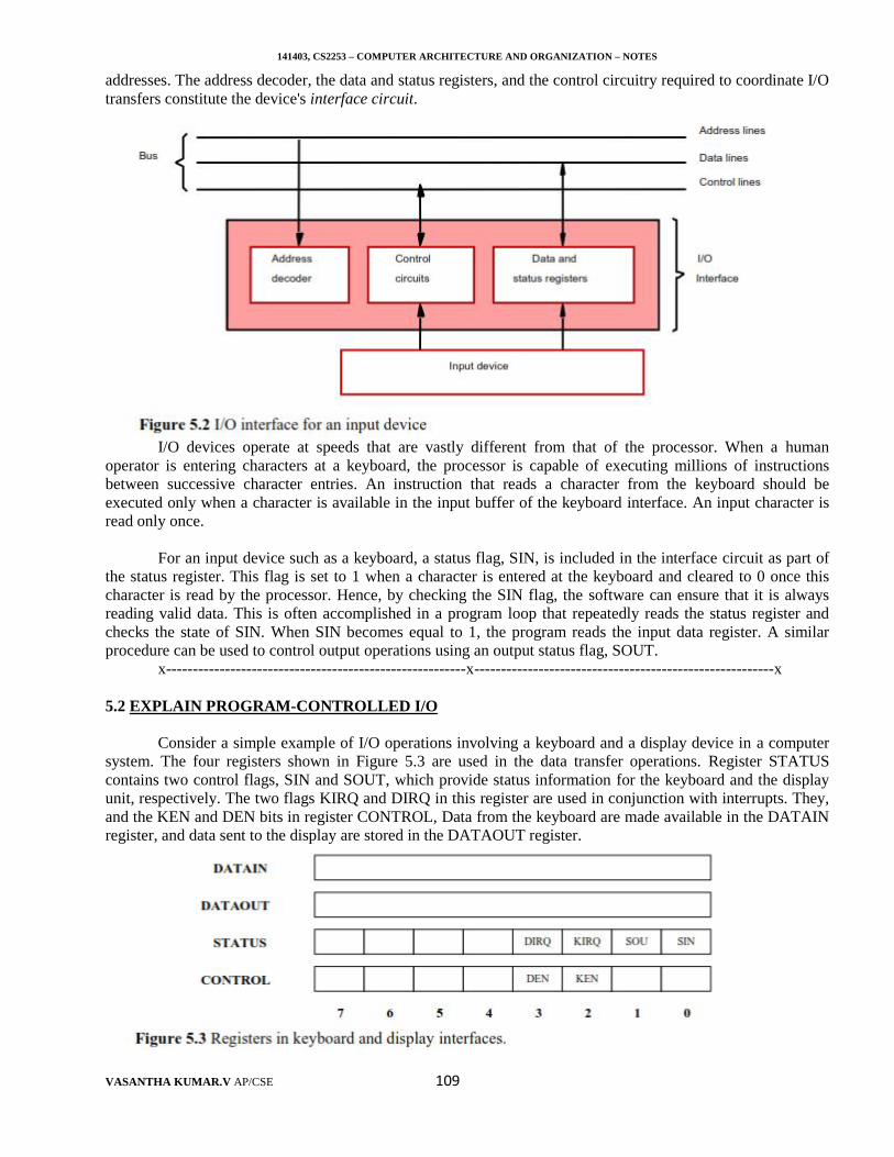
141403, CS2253 – COMPUTER ARCHITECTURE AND ORGANIZATION – NOTES
VASANTHA KUMAR.V AP/CSE 109
addresses. The address decoder, the data and status registers, and the control circuitry required to coordinate I/Otransfers constitute the device's interface circuit.
I/O devices operate at speeds that are vastly different from that of the processor. When a humanoperator is entering characters at a keyboard, the processor is capable of executing millions of instructionsbetween successive character entries. An instruction that reads a character from the keyboard should beexecuted only when a character is available in the input buffer of the keyboard interface. An input character isread only once.
For an input device such as a keyboard, a status flag, SIN, is included in the interface circuit as part ofthe status register. This flag is set to 1 when a character is entered at the keyboard and cleared to 0 once thischaracter is read by the processor. Hence, by checking the SIN flag, the software can ensure that it is alwaysreading valid data. This is often accomplished in a program loop that repeatedly reads the status register andchecks the state of SIN. When SIN becomes equal to 1, the program reads the input data register. A similarprocedure can be used to control output operations using an output status flag, SOUT.
x--------------------------------------------------------x--------------------------------------------------------x
5.2 EXPLAIN PROGRAM-CONTROLLED I/O
Consider a simple example of I/O operations involving a keyboard and a display device in a computersystem. The four registers shown in Figure 5.3 are used in the data transfer operations. Register STATUScontains two control flags, SIN and SOUT, which provide status information for the keyboard and the displayunit, respectively. The two flags KIRQ and DIRQ in this register are used in conjunction with interrupts. They,and the KEN and DEN bits in register CONTROL, Data from the keyboard are made available in the DATAINregister, and data sent to the display are stored in the DATAOUT register.
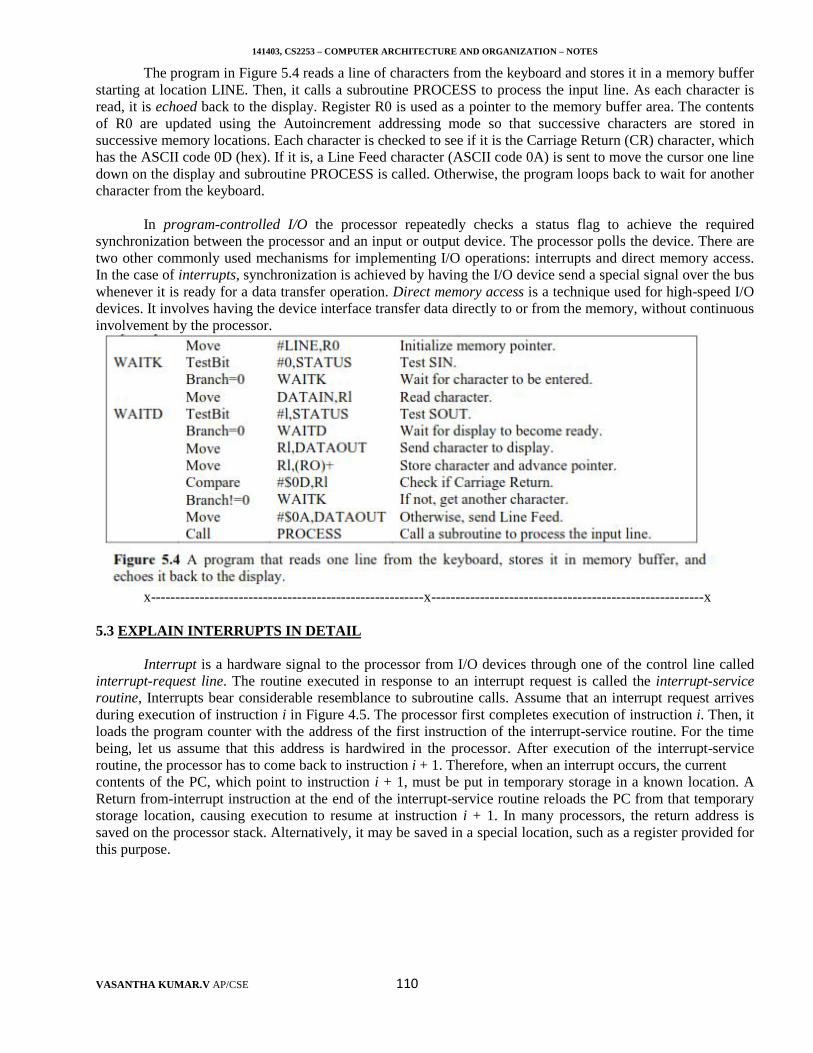
141403, CS2253 – COMPUTER ARCHITECTURE AND ORGANIZATION – NOTES
VASANTHA KUMAR.V AP/CSE 110
The program in Figure 5.4 reads a line of characters from the keyboard and stores it in a memory bufferstarting at location LINE. Then, it calls a subroutine PROCESS to process the input line. As each character isread, it is echoed back to the display. Register R0 is used as a pointer to the memory buffer area. The contentsof R0 are updated using the Autoincrement addressing mode so that successive characters are stored insuccessive memory locations. Each character is checked to see if it is the Carriage Return (CR) character, whichhas the ASCII code 0D (hex). If it is, a Line Feed character (ASCII code 0A) is sent to move the cursor one linedown on the display and subroutine PROCESS is called. Otherwise, the program loops back to wait for anothercharacter from the keyboard.
In program-controlled I/O the processor repeatedly checks a status flag to achieve the requiredsynchronization between the processor and an input or output device. The processor polls the device. There aretwo other commonly used mechanisms for implementing I/O operations: interrupts and direct memory access.In the case of interrupts, synchronization is achieved by having the I/O device send a special signal over the buswhenever it is ready for a data transfer operation. Direct memory access is a technique used for high-speed I/Odevices. It involves having the device interface transfer data directly to or from the memory, without continuousinvolvement by the processor.
x--------------------------------------------------------x--------------------------------------------------------x
5.3 EXPLAIN INTERRUPTS IN DETAIL
Interrupt is a hardware signal to the processor from I/O devices through one of the control line calledinterrupt-request line. The routine executed in response to an interrupt request is called the interrupt-serviceroutine, Interrupts bear considerable resemblance to subroutine calls. Assume that an interrupt request arrivesduring execution of instruction i in Figure 4.5. The processor first completes execution of instruction i. Then, itloads the program counter with the address of the first instruction of the interrupt-service routine. For the timebeing, let us assume that this address is hardwired in the processor. After execution of the interrupt-serviceroutine, the processor has to come back to instruction i + 1. Therefore, when an interrupt occurs, the currentcontents of the PC, which point to instruction i + 1, must be put in temporary storage in a known location. AReturn from-interrupt instruction at the end of the interrupt-service routine reloads the PC from that temporarystorage location, causing execution to resume at instruction i + 1. In many processors, the return address issaved on the processor stack. Alternatively, it may be saved in a special location, such as a register provided forthis purpose.
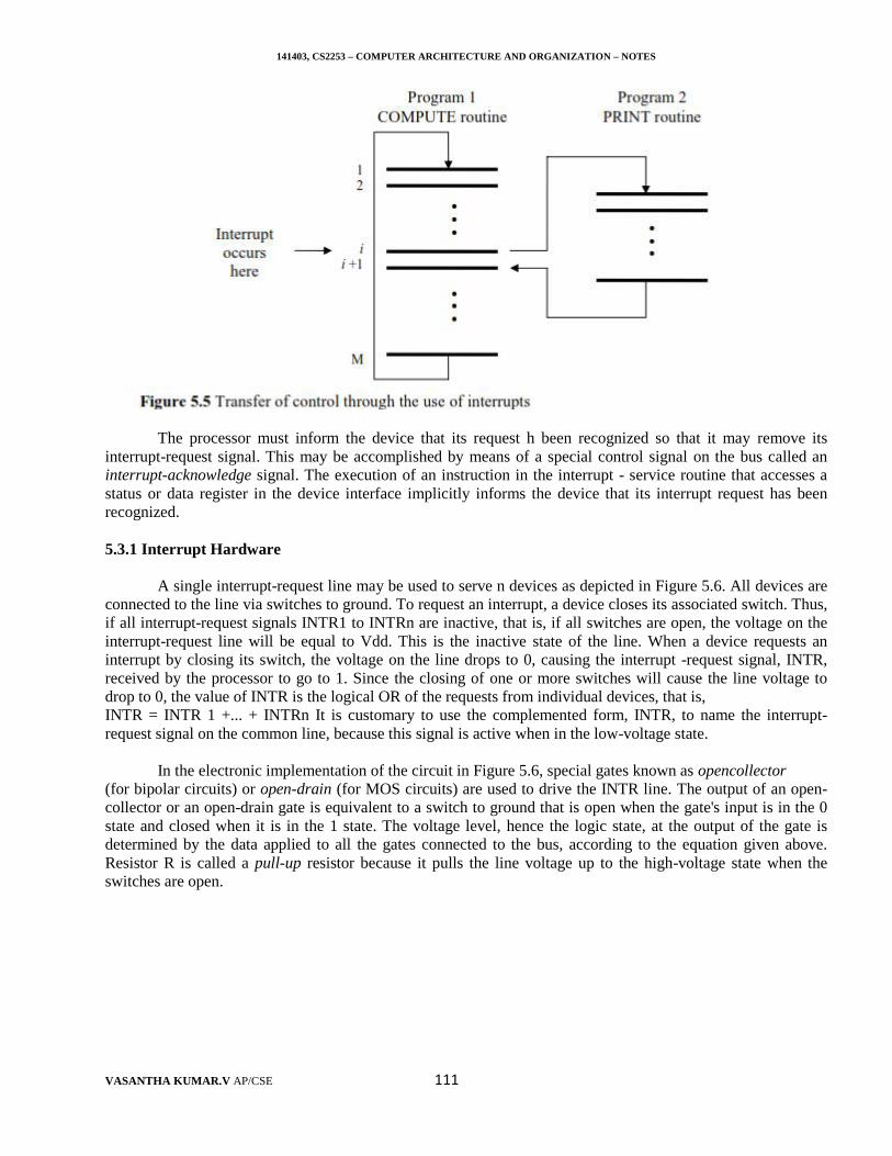
141403, CS2253 – COMPUTER ARCHITECTURE AND ORGANIZATION – NOTES
VASANTHA KUMAR.V AP/CSE 111
The processor must inform the device that its request h been recognized so that it may remove itsinterrupt-request signal. This may be accomplished by means of a special control signal on the bus called aninterrupt-acknowledge signal. The execution of an instruction in the interrupt - service routine that accesses astatus or data register in the device interface implicitly informs the device that its interrupt request has beenrecognized.
5.3.1 Interrupt Hardware
A single interrupt-request line may be used to serve n devices as depicted in Figure 5.6. All devices areconnected to the line via switches to ground. To request an interrupt, a device closes its associated switch. Thus,if all interrupt-request signals INTR1 to INTRn are inactive, that is, if all switches are open, the voltage on theinterrupt-request line will be equal to Vdd. This is the inactive state of the line. When a device requests aninterrupt by closing its switch, the voltage on the line drops to 0, causing the interrupt -request signal, INTR,received by the processor to go to 1. Since the closing of one or more switches will cause the line voltage todrop to 0, the value of INTR is the logical OR of the requests from individual devices, that is,INTR = INTR 1 +... + INTRn It is customary to use the complemented form, INTR, to name the interrupt-request signal on the common line, because this signal is active when in the low-voltage state.
In the electronic implementation of the circuit in Figure 5.6, special gates known as opencollector(for bipolar circuits) or open-drain (for MOS circuits) are used to drive the INTR line. The output of an open-collector or an open-drain gate is equivalent to a switch to ground that is open when the gate's input is in the 0state and closed when it is in the 1 state. The voltage level, hence the logic state, at the output of the gate isdetermined by the data applied to all the gates connected to the bus, according to the equation given above.Resistor R is called a pull-up resistor because it pulls the line voltage up to the high-voltage state when theswitches are open.
141403, CS2253 – COMPUTER ARCHITECTURE AND ORGANIZATION – NOTES
VASANTHA KUMAR.V AP/CSE 112
5.3.2 Enabling and Disabling Interrupts
There are many situations in which the processor should ignore interrupt requests. For example, in thecase of the Compute-Print program of Figure 5.5, an interrupt request from the printer should be accepted onlyif there are output lines to be printed. After printing the last line of a set of n lines, interrupts should be disableduntil another set becomes available for printing. A simple way is to provide machine instructions, such asInterrupt-enable and Interrupt disable. The processor hardware ignores the interrupt-request line until theexecution of the first instruction of the interrupt-service routine has been completed. Then, by using anInterrupt-disable instruction as the first instruction in the interrupt-service routine, the programmer can ensurethat no further interruptions will occur until an Interrupt-enable instruction is executed.
Typically, the Interrupt- enable instruction will be the last instruction in the interrupt-service routinebefore the Return-from-interrupt instruction. The processor must guarantee that execution of the Returnfrom-interrupt instruction is completed before ¬further interruption can occur. The second option, which is suitablefor a simple processor with only one interrupt- request line, is to have the process or automatically disableinterrupts before starting the execution of the interrupt-service routine. After saving the contents of the PC andthe processor status register (PS) on the stack, the processor performs the equivalent of executing an Interrupt -disable instruction. It is often the case that one bit in the PS register, called Interrupt-enable, indicates whetherinterrupts are enabled. An interrupt request received while this bit is equal to 1 will be accepted. After savingthe contents of the PS on the stack, with the Interrupt-enable bit equal to 1, the processor clears the Interrupt-enable bit in its PS register, thus disabling further interrupts. When a Return-from interrupt instruction isexecuted, the contents of the PS are restored from the stack, setting the Interrupt-enable bit back to 1. Hence,interrupts are again enabled.
In the third option, the processor has a special interrupt-request line for which the interrupt handlingcircuit responds only to the leading edge of the signal. Such a line is said to be edge triggered. In this case, theprocessor will receive only one request, regardless of how long the line is activated. Hence, there is no dangerof multiple interruptions and no need to explicitly disable interrupt requests from this line. Before proceeding tostudy more complex aspects of interrupts, let us summarize the sequence of events involved in handling aninterrupt request from a single device. Assuming that interrupts are enabled, the following is a typical scenario:1. The device raises an interrupt request.2. The processor interrupts the program currently being executed.3. Interrupts are disabled by changing the control bits in the PS (except in the case of edgetriggered interrupts).4. The device is informed that its request has been recognized, and in response, it deactivates the interrupt-request signal.5. The action requested by the interrupt is performed by the interrupt-service routine.
141403, CS2253 – COMPUTER ARCHITECTURE AND ORGANIZATION – NOTES
VASANTHA KUMAR.V AP/CSE 113
6. Interrupts are enabled and execution of the interrupted program is resumed.
5.3.3 HANDLING MULTIPLE DEVICES (May come separately for 8 marks)
Let us now consider the situation where a number of devices capable of initiating interrupts areconnected to the processor. Because these devices are operationally independent, there is no definite order inwhich they will generate interrupts. For example, device X may request an interrupt while an interrupt causedby device Y is being serviced, or several devices may request interrupts at exactly the same time. This gives riseto a number of questions:1. How can the processor recognize the device requesting an interrupt?2. Given that different devices are likely to require different interrupt -service routines, how can the processorobtain the starting address of the appropriate routine in each case?3. Should a device be allowed to interrupt the processor while another interrupt is being serviced?4. How should two or more simultaneous interrupt requests be handled?
If two devices have activated the line at the same time, it must be possible to break the tie and elect oneof the two requests for service. When the interrupt-service routine for the selected device has been completed,the second request can be serviced.
Vectored interrupts
To reduce the time involved in the polling process, a device requesting an interrupt may identify itselfdirectly to the processor. Then, the processor can immediately start executing the corresponding interrupt-service routine. The term vectored interrupts refers to all interrupt - handling schemes based on this approach.
A device requesting an interrupt can identify itself by sending a special code to the processor over thebus. This enables the processor to identify individual devices even if they share a single interrupt-request line.The code supplied by the device may represent the starting address of the interrupt-service routine for thatdevice. The code length is typically in the range of 4 to 8 bits. The remainder of the address is supplied by theprocessor based on the area in its memory where the addresses for interrupt-service routines are located.
This arrangement implies that the interrupt-service routine for a given device must always start at thesame location. The programmer can gain some flexibility by storing in this location an instruction that causes abranch to the appropriate routine. In many computers, this is done automatically by the interrupt-handlingmechanism. The location pointed to by the interrupting device is used to store the starting address of theinterrupt-service routine. The processor reads this address, called the interrupt vector, and loads it into the PC.The interrupt vector may also include a new value for the processor status register
.In most computers, I/O devices send the interrupt-vector code over the data bus, using the bus control
signals to ensure that devices do not interfere with each other. When a device sends an interrupt request, theprocessor may not be ready to receive the interrupt-vector code immediately. For example, it must firstcomplete the execution of the current instruction, which may require the use of the bus. There may be furtherdelays if interrupts happen to be disabled at the time the request is raised. The interrupting device must wait toput data on the bus only when the processor is ready to receive it. When the processor is ready to receive theinterrupt-vector code, it activates the interrupt-acknowledge line, INTA. The I/O device responds by sending itsinterrupt- vector code and turning off the INTR signal.
Interrupt nesting
I/O devices should be organized in a priority structure. An interrupt request from a high priority deviceshould be accepted while the processor is servicing another request from a lower priority device. A multiple-level priority organization means that during execution of an interrupt service routine, interrupt requests will beaccepted from some devices but not from others, depending upon the device's priority. To implement thisscheme, priority level can be assigned to the processor that can be changed by the program.
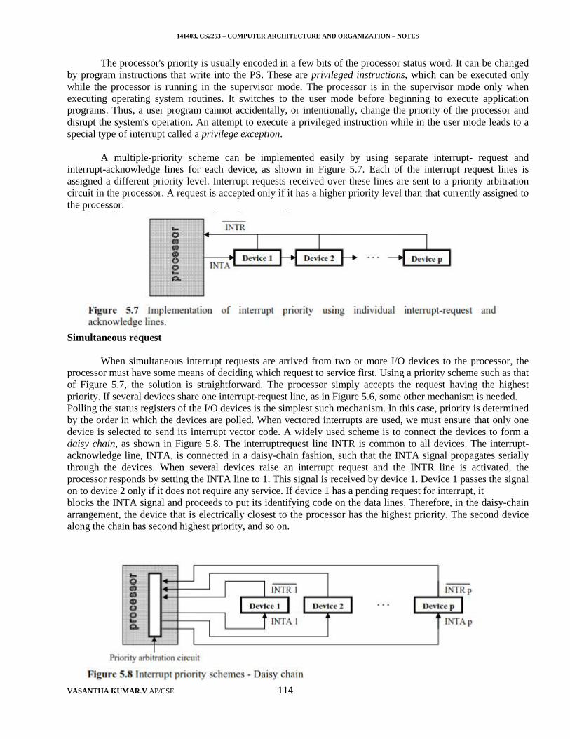
141403, CS2253 – COMPUTER ARCHITECTURE AND ORGANIZATION – NOTES
VASANTHA KUMAR.V AP/CSE 114
The processor's priority is usually encoded in a few bits of the processor status word. It can be changedby program instructions that write into the PS. These are privileged instructions, which can be executed onlywhile the processor is running in the supervisor mode. The processor is in the supervisor mode only whenexecuting operating system routines. It switches to the user mode before beginning to execute applicationprograms. Thus, a user program cannot accidentally, or intentionally, change the priority of the processor anddisrupt the system's operation. An attempt to execute a privileged instruction while in the user mode leads to aspecial type of interrupt called a privilege exception.
A multiple-priority scheme can be implemented easily by using separate interrupt- request andinterrupt-acknowledge lines for each device, as shown in Figure 5.7. Each of the interrupt request lines isassigned a different priority level. Interrupt requests received over these lines are sent to a priority arbitrationcircuit in the processor. A request is accepted only if it has a higher priority level than that currently assigned tothe processor.
Simultaneous request
When simultaneous interrupt requests are arrived from two or more I/O devices to the processor, theprocessor must have some means of deciding which request to service first. Using a priority scheme such as thatof Figure 5.7, the solution is straightforward. The processor simply accepts the request having the highestpriority. If several devices share one interrupt-request line, as in Figure 5.6, some other mechanism is needed.Polling the status registers of the I/O devices is the simplest such mechanism. In this case, priority is determinedby the order in which the devices are polled. When vectored interrupts are used, we must ensure that only onedevice is selected to send its interrupt vector code. A widely used scheme is to connect the devices to form adaisy chain, as shown in Figure 5.8. The interruptrequest line INTR is common to all devices. The interrupt-acknowledge line, INTA, is connected in a daisy-chain fashion, such that the INTA signal propagates seriallythrough the devices. When several devices raise an interrupt request and the INTR line is activated, theprocessor responds by setting the INTA line to 1. This signal is received by device 1. Device 1 passes the signalon to device 2 only if it does not require any service. If device 1 has a pending request for interrupt, itblocks the INTA signal and proceeds to put its identifying code on the data lines. Therefore, in the daisy-chainarrangement, the device that is electrically closest to the processor has the highest priority. The second devicealong the chain has second highest priority, and so on.
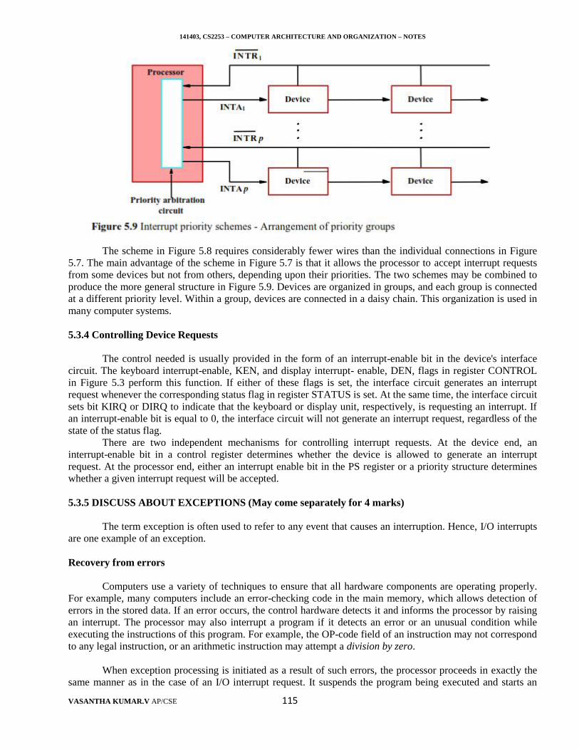
141403, CS2253 – COMPUTER ARCHITECTURE AND ORGANIZATION – NOTES
VASANTHA KUMAR.V AP/CSE 115
The scheme in Figure 5.8 requires considerably fewer wires than the individual connections in Figure5.7. The main advantage of the scheme in Figure 5.7 is that it allows the processor to accept interrupt requestsfrom some devices but not from others, depending upon their priorities. The two schemes may be combined toproduce the more general structure in Figure 5.9. Devices are organized in groups, and each group is connectedat a different priority level. Within a group, devices are connected in a daisy chain. This organization is used inmany computer systems.
5.3.4 Controlling Device Requests
The control needed is usually provided in the form of an interrupt-enable bit in the device's interfacecircuit. The keyboard interrupt-enable, KEN, and display interrupt- enable, DEN, flags in register CONTROLin Figure 5.3 perform this function. If either of these flags is set, the interface circuit generates an interruptrequest whenever the corresponding status flag in register STATUS is set. At the same time, the interface circuitsets bit KIRQ or DIRQ to indicate that the keyboard or display unit, respectively, is requesting an interrupt. Ifan interrupt-enable bit is equal to 0, the interface circuit will not generate an interrupt request, regardless of thestate of the status flag.
There are two independent mechanisms for controlling interrupt requests. At the device end, aninterrupt-enable bit in a control register determines whether the device is allowed to generate an interruptrequest. At the processor end, either an interrupt enable bit in the PS register or a priority structure determineswhether a given interrupt request will be accepted.
5.3.5 DISCUSS ABOUT EXCEPTIONS (May come separately for 4 marks)
The term exception is often used to refer to any event that causes an interruption. Hence, I/O interruptsare one example of an exception.
Recovery from errors
Computers use a variety of techniques to ensure that all hardware components are operating properly.For example, many computers include an error-checking code in the main memory, which allows detection oferrors in the stored data. If an error occurs, the control hardware detects it and informs the processor by raisingan interrupt. The processor may also interrupt a program if it detects an error or an unusual condition whileexecuting the instructions of this program. For example, the OP-code field of an instruction may not correspondto any legal instruction, or an arithmetic instruction may attempt a division by zero.
When exception processing is initiated as a result of such errors, the processor proceeds in exactly thesame manner as in the case of an I/O interrupt request. It suspends the program being executed and starts an
141403, CS2253 – COMPUTER ARCHITECTURE AND ORGANIZATION – NOTES
VASANTHA KUMAR.V AP/CSE 116
exception-service routine. This routine takes appropriate action to recover from the error, if possible, or toinform the user about it. Recall that in the case of an I/O interrupt, the processor completes execution of theinstruction in progress before accepting the interrupt. However, when an interrupt is caused by an error,execution of the interrupted instruction cannot usually be completed, and the processor begins exceptionprocessing immediately.
Debugging
Another important type of exception is used as an aid in debugging programs. System software usuallyincludes a program called a debugger, which helps the programmer find errors in a program. The debugger usesexceptions to provide two important facilities called trace and breakpoints. When a processor is operating in thetrace mode, an exception occurs after execution of every instruction, using the debugging program as theexception-service routine. The debugging program enables the user to examine the contents of registers,memory locations, and so on. On return from the debugging program, the next instruction in the program beingdebugged is executed, then the debugging program is activated again. The trace exception is disabled duringthe execution of the debugging program.
Breakpoints provide a similar facility, except that the program being debugged is interrupted only atspecific points selected by the user. An instruction called Trap or Software interrupt is usually provided for thispurpose. Execution of this instruction results in exactly the same actions as when a hardware interrupt request isreceived. While debugging a program, the user may wish to interrupt program execution after instruction i. Thedebugging routine saves instruction i + 1 and replaces it with a software interrupt instruction. When the programis executed and reaches that point, it is interrupted and the debugging routine is activated. This gives the user achance to examine memory and register contents. When the user is ready to continue executing the programbeing debugged, the debugging routine restores the saved instruction that was at location i + 1 and executes aReturn-from-interrupt instruction.
Privilege exception
To protect the operating system of a computer from being corrupted by user programs, certaininstructions can be executed only while the processor is in the supervisor mode. These are called privilegedinstructions. For example, when the processor is running in the user mode, it will not execute an instruction thatchanges the priority level of the processor or that enables a user program to access areas in the computermemory that have been allocated to other users. An attempt to execute such an instruction will produce aprivilege exception, causing the processor to switch to the supervisor mode and begin executing an appropriateroutine in the operating system.
5.3.6 USE OF INTERRUPTS IN OPERATING SYSTEMS (May come separately for 6 marks)
The operating system (OS) is responsible for coordinating all activities within a computer. It makesextensive use of interrupts to perform I/O operations and communicate with and control the execution of userprograms. The operating system incorporates the interrupt-service routines (ISR) for all devices connected to acomputer. Application programs do not perform I/O operations themselves. An operating system provides avariety of services to application programs. To facilitate the implementation of these services, most processorshave several different software interrupt instructions, each with its own interrupt vector. They can be used tocall different parts of the OS.
In a computer that has both a supervisor and a user mode, the processor switches its operation tosupervisor mode at the time it accepts an interrupt request. It does so by setting a bit in the processor statusregister after saving the old contents of that register on the stack. Thus, when an application program calls the asby a software interrupt instruction, the processor automatically switches to supervisor mode, giving the ascomplete access to the computer's resources. When the as executes a Return-from-interrupt instruction, theprocessor status word belonging to the application program is restored from the stack. As a result, the processorswitches back to the user mode.
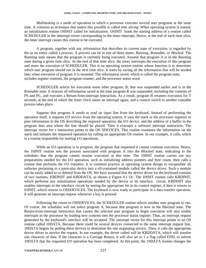
141403, CS2253 – COMPUTER ARCHITECTURE AND ORGANIZATION – NOTES
VASANTHA KUMAR.V AP/CSE 117
Multitasking is a mode of operation in which a processor executes several user programs at the sametime. A common as technique that makes this possible is called time slicing. When operating system is started,an initialization routine OSINIT called for initialization. OSINIT loads the starting address of a routine calledSCHEDULER in the interrupt vector corresponding to the timer interrupt. Hence, at the end of each time slice,the timer interrupt causes this routine to be executed.
A program, together with any information that describes its current state of execution, is regarded bythe as an entity called a process. A process can be in one of three states: Running, Runnable, or Blocked. TheRunning state means that the program is currently being executed. Assume that program A is in the Runningstate during a given time slice. At the end of that time slice, the timer interrupts the execution of this programand starts the execution of SCHEDULER. This is an operating system routine whose function is to determinewhich user program should run in the next time slice. It starts by saving all the information that will be neededlater when execution of program A is resumed. The information saved, which is called the program state,includes register contents, the program counter, and the processor status word.
SCHEDULER selects for execution some other program, B, that was suspended earlier and is in theRunnable state. It restores all information saved at the time program R was suspended, including the contents ofPS and PC, and executes a Retum-from-interrupt instruction. As a result, program B resumes execution for Tseconds, at the end of which the timer clock raises an interrupt again, and a context switch to another runnableprocess takes place.
Suppose that program A needs to read an input line from the keyboard. Instead of performing theoperation itself, it requests I/O service from the operating system. It uses the stack or the processor registers topass information to the OS describing the required operation, the I/O device, and the address of a buffer in theprogram data area where the line should be placed. Then it executes a software interrupt instruction. Theinterrupt vector for s instruction points to the OS SERVICES. This routine examines the information on thestack and initiates the requested operation by calling an appropriate OS routine. In our example, it calls, whichis a routine responsible for starting I/O operations.
While an I/O operation is in progress, the program that requested it cannot continue execution. Hence,the 10INIT routine sets the process associated with program A into the Blocked state, indicating to thescheduler that the program cannot resume execution at this time. The 10INIT routine carries out anypreparations needed for the I/O operation, such as initializing address pointers and byte count, then calls aroutine that performs the I/O transfers. It is common practice in operating system design to encapsulate allsoftware pertaining to a particular device into a elf-contained module called the device driver. Such a modulecan be easily added to or deleted from the OS. We have assumed that the device driver for the keyboard consistsof two routines, KBDINIT and KBDDATA, as shown n Figure 4.1 Oc. The 10INIT routine calls KBDINIT,which performs any initialization operations needed by the device or its interface circuit. KBDINIT alsoenables interrupts in the interface circuit by setting the appropriate bit in its control register, d then it returns toIOINIT, which returns to OSSERVICES. The keyboard is now ready to participate in a data transfer operation.It will generate an interrupt request whenever a key is pressed.
Following the return to OSSERVICES, the SCHEDULER routine selects another user program to run.Of course, the scheduler will not select program A, because that program is now in the Blocked state. TheReturn-from-interrupt instruction that causes the selected user program to begin execution will also enableinterrupts in the processor by loading new contents into the processor status register. Thus, an interrupt requestgenerated by the keyboard's interface will be accepted. The interrupt vector for this interrupt points to an OSroutine called 10DATA. Because there could be several devices connected to the same interrupt request line,10DATA begins by polling these devices to determine the one requesting service. Then, it calls the appropriatedevice driver to service the request. In our example, the driver called will be KBDDATA, which will transferone character of data. If the character is a Carriage Return, it will also set to 1 a flag called END, to inform10DATA that the requested I/O operation has been completed. At this point, the 10DATA routine changes the
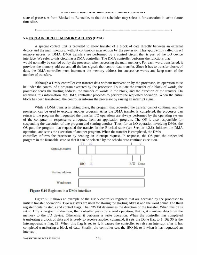
141403, CS2253 – COMPUTER ARCHITECTURE AND ORGANIZATION – NOTES
VASANTHA KUMAR.V AP/CSE 118
state of process A from Blocked to Runnable, so that the scheduler may select it for execution in some futuretime slice.
x--------------------------------------------------------x--------------------------------------------------------x
5.4 EXPLAIN DIRECT MEMORY ACCESS (DMA)
A special control unit is provided to allow transfer of a block of data directly between an externaldevice and the main memory, without continuous intervention by the processor. This approach is called directmemory access, or DMA. DMA transfers are performed by a control circuit that is part of the I/O deviceinterface. We refer to this circuit as a DMA controller. The DMA controller performs the functions thatwould normally be carried out by the processor when accessing the main memory. For each word transferred, itprovides the memory address and all the bus signals that control data transfer. Since it has to transfer blocks ofdata, the DMA controller must increment the memory address for successive words and keep track of thenumber of transfers.
Although a DMA controller can transfer data without intervention by the processor, its operation mustbe under the control of a program executed by the processor. To initiate the transfer of a block of words, theprocessor sends the starting address, the number of words in the block, and the direction of the transfer. Onreceiving this information, the DMA controller proceeds to perform the requested operation. When the entireblock has been transferred, the controller informs the processor by raising an interrupt signal.
While a DMA transfer is taking place, the program that requested the transfer cannot continue, and theprocessor can be used to execute another program. After the DMA transfer is completed, the processor canreturn to the program that requested the transfer. I/O operations are always performed by the operating systemof the computer in response to a request from an application program. The OS is also responsible forsuspending the execution of one program and starting another. Thus, for an I/O operation involving DMA, theOS puts the program that requested the transfer in the Blocked state (see Section 4.2.6), initiates the DMAoperation, and starts the execution of another program. When the transfer is completed, the DMAcontroller informs the processor by sending an interrupt request. In response, the OS puts the suspendedprogram in the Runnable state so that it can be selected by the scheduler to continue execution.
Figure 5.10 shows an example of the DMA controller registers that are accessed by the processor toinitiate transfer operations. Two registers are used for storing the starting address and the word count. The thirdregister contains status and control flags. The R/W bit determines the direction of the transfer. When this bit isset to 1 by a program instruction, the controller performs a read operation, that is, it transfers data from thememory to the I/O device. Otherwise, it performs a write operation. When the controller has completedtransferring a block of data and is ready to receive another command, it sets the Done flag to 1. Bit 30 is theInterrupt-enable flag, IE. When this flag is set to 1, it causes the controller to raise an interrupt after it hascompleted transferring a block of data. Finally, the controller sets the IRQ bit to 1 when it has requested aninterrupt.
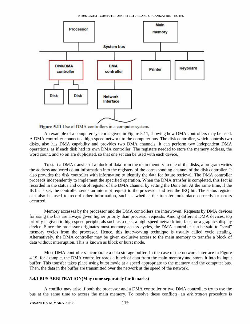
141403, CS2253 – COMPUTER ARCHITECTURE AND ORGANIZATION – NOTES
VASANTHA KUMAR.V AP/CSE 119
An example of a computer system is given in Figure 5.11, showing how DMA controllers may be used.A DMA controller connects a high-speed network to the computer bus. The disk controller, which controls twodisks, also has DMA capability and provides two DMA channels. It can perform two independent DMAoperations, as if each disk had its own DMA controller. The registers needed to store the memory address, theword count, and so on are duplicated, so that one set can be used with each device.
To start a DMA transfer of a block of data from the main memory to one of the disks, a program writesthe address and word count information into the registers of the corresponding channel of the disk controller. Italso provides the disk controller with information to identify the data for future retrieval. The DMA controllerproceeds independently to implement the specified operation. When the DMA transfer is completed, this fact isrecorded in the status and control register of the DMA channel by setting the Done bit. At the same time, if theIE bit is set, the controller sends an interrupt request to the processor and sets the IRQ bit. The status registercan also be used to record other information, such as whether the transfer took place correctly or errorsoccurred.
Memory accesses by the processor and the DMA controllers are interwoven. Requests by DMA devicesfor using the bus are always given higher priority than processor requests. Among different DMA devices, toppriority is given to high-speed peripherals such as a disk, a high-speed network interface, or a graphics displaydevice. Since the processor originates most memory access cycles, the DMA controller can be said to "steal"memory cycles from the processor. Hence, this interweaving technique is usually called cycle stealing.Alternatively, the DMA controller may be given exclusive access to the main memory to transfer a block ofdata without interruption. This is known as block or burst mode.
Most DMA controllers incorporate a data storage buffer. In the case of the network interface in Figure4.19, for example, the DMA controller reads a block of data from the main memory and stores it into its inputbuffer. This transfer takes place using burst mode at a speed appropriate to the memory and the computer bus.Then, the data in the buffer are transmitted over the network at the speed of the network.
5.4.1 BUS ARBITRATION(May come separately for 6 marks)
A conflict may arise if both the processor and a DMA controller or two DMA controllers try to use thebus at the same time to access the main memory. To resolve these conflicts, an arbitration procedure is
141403, CS2253 – COMPUTER ARCHITECTURE AND ORGANIZATION – NOTES
VASANTHA KUMAR.V AP/CSE 120
implemented on the bus to coordinate the activities of all devices requesting memory transfers. The device thatinitiates data transfers on the bus at any given time is called the bus master. When the current masterrelinquishes control of the bus, another device can acquire this status. Bus arbitration is the process by whichthe next device to become the bus master is selected and bus mastership is transferred to it. The selection of thebus master must take into account the needs of various devices by establishing a priority system for gainingaccess to the bus. There are two approaches to bus arbitration: centralized and distributed. In centralizedarbitration, a single bus arbiter performs the required arbitration. In distributed arbitration, all devicesparticipate in the selection of the next bus master.
Centralized arbitration
The bus arbiter may be the processor or a separate unit connected to the bus. Figure 5.12 illustrates abasic arrangement in which the processor contains the bus arbitration circuitry.
The processor is normally the bus master unless it grants bus mastership to one of the DMA controllers.A DMA controller indicates that it needs to become the bus master by activating the Bus-Request line, BR, Thisis an open-drain line for the same reasons that the Interrupt- Request line in Figure 5.6 is an open-drain line.The signal on the Bus-Request line is the logical OR of the bus requests from all the devices connected to it.When Bus-Request is activated, the processor activates the Bus-Grant signal, BG 1, indicating to the DMAcontrollers that they may use the bus when it becomes free. This signal is connected to all DMA controllersusing a daisychain arrangement. Thus, if DMA controller 1 is requesting the bus, it blocks the propagation ofthe grant signal to other devices. Otherwise, it passes the grant downstream by asserting BG2.
The current bus master indicates to all device s that i t is using the bus by activating another opencollector line called Busy, BBSY. Hence, after receiving the Bus-Grant signal, a DMA controller waits for Bus-Busy to become inactive, then assumes mastership of the bus. At this time, it activates Bus-Busy to preventother devices from using the bus at the same time. The timing diagram in Figure 5.13 shows the sequence ofevents for the devices in Figure 5.12 as DMA controller 2 requests and acquires bus mastership and laterreleases the bus. During its tenure as the bus master, it may perform one or more data transfer operations,depending on whether it is operating in the cycle stealing or block mode. After it releases the bus, the processorresumes bus mastership. This figure shows the causal relationships among the signals involved in the arbitrationprocess. Details of timing, which vary significantly from one computer bus to another, are not shown.
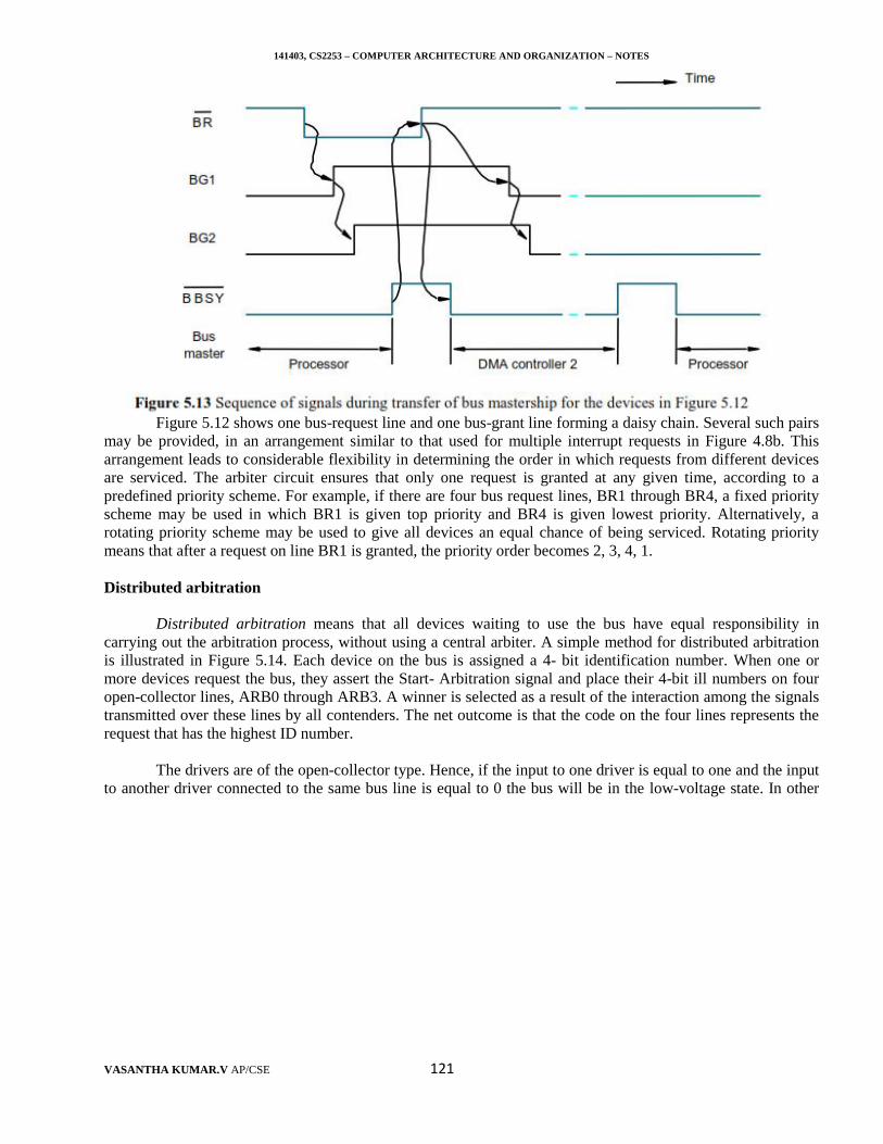
141403, CS2253 – COMPUTER ARCHITECTURE AND ORGANIZATION – NOTES
VASANTHA KUMAR.V AP/CSE 121
Figure 5.12 shows one bus-request line and one bus-grant line forming a daisy chain. Several such pairsmay be provided, in an arrangement similar to that used for multiple interrupt requests in Figure 4.8b. Thisarrangement leads to considerable flexibility in determining the order in which requests from different devicesare serviced. The arbiter circuit ensures that only one request is granted at any given time, according to apredefined priority scheme. For example, if there are four bus request lines, BR1 through BR4, a fixed priorityscheme may be used in which BR1 is given top priority and BR4 is given lowest priority. Alternatively, arotating priority scheme may be used to give all devices an equal chance of being serviced. Rotating prioritymeans that after a request on line BR1 is granted, the priority order becomes 2, 3, 4, 1.
Distributed arbitration
Distributed arbitration means that all devices waiting to use the bus have equal responsibility incarrying out the arbitration process, without using a central arbiter. A simple method for distributed arbitrationis illustrated in Figure 5.14. Each device on the bus is assigned a 4- bit identification number. When one ormore devices request the bus, they assert the Start- Arbitration signal and place their 4-bit ill numbers on fouropen-collector lines, ARB0 through ARB3. A winner is selected as a result of the interaction among the signalstransmitted over these lines by all contenders. The net outcome is that the code on the four lines represents therequest that has the highest ID number.
The drivers are of the open-collector type. Hence, if the input to one driver is equal to one and the inputto another driver connected to the same bus line is equal to 0 the bus will be in the low-voltage state. In other
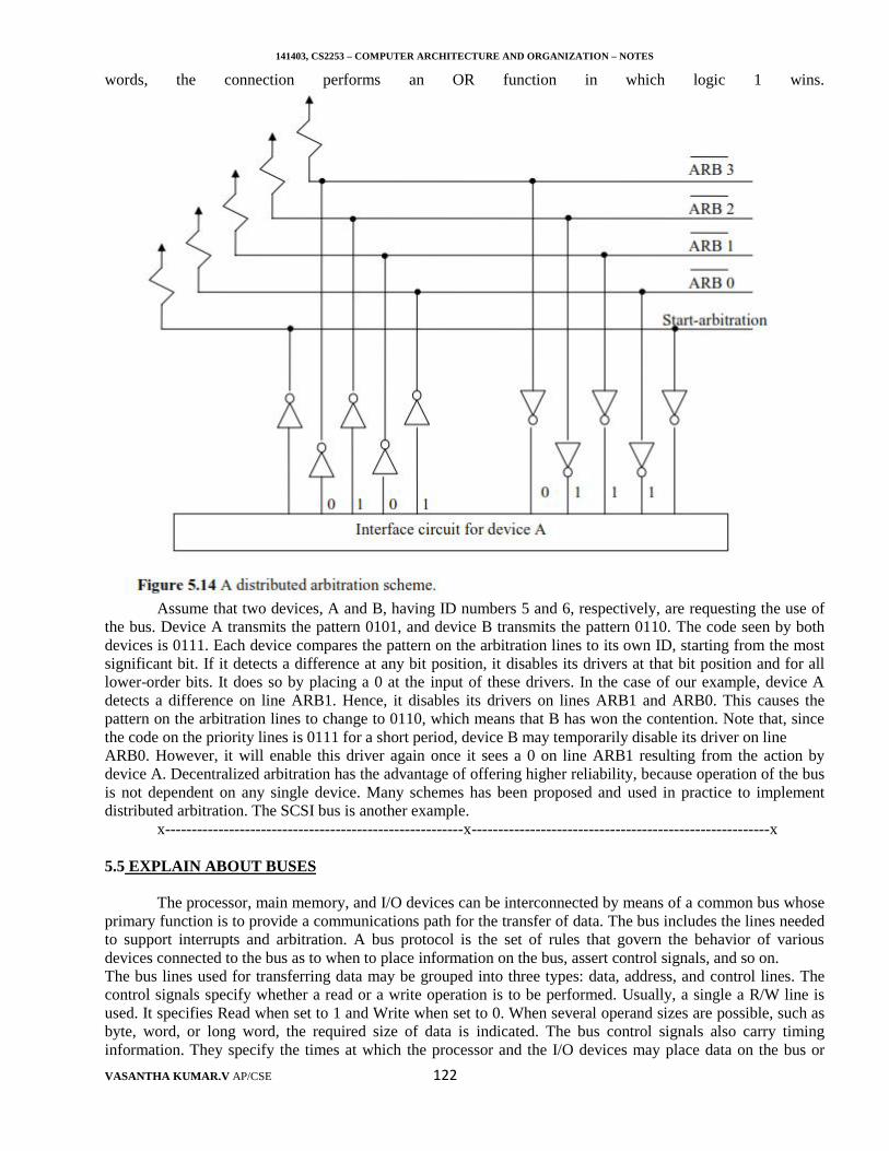
141403, CS2253 – COMPUTER ARCHITECTURE AND ORGANIZATION – NOTES
VASANTHA KUMAR.V AP/CSE 122
words, the connection performs an OR function in which logic 1 wins.
Assume that two devices, A and B, having ID numbers 5 and 6, respectively, are requesting the use ofthe bus. Device A transmits the pattern 0101, and device B transmits the pattern 0110. The code seen by bothdevices is 0111. Each device compares the pattern on the arbitration lines to its own ID, starting from the mostsignificant bit. If it detects a difference at any bit position, it disables its drivers at that bit position and for alllower-order bits. It does so by placing a 0 at the input of these drivers. In the case of our example, device Adetects a difference on line ARB1. Hence, it disables its drivers on lines ARB1 and ARB0. This causes thepattern on the arbitration lines to change to 0110, which means that B has won the contention. Note that, sincethe code on the priority lines is 0111 for a short period, device B may temporarily disable its driver on lineARB0. However, it will enable this driver again once it sees a 0 on line ARB1 resulting from the action bydevice A. Decentralized arbitration has the advantage of offering higher reliability, because operation of the busis not dependent on any single device. Many schemes has been proposed and used in practice to implementdistributed arbitration. The SCSI bus is another example.
x--------------------------------------------------------x--------------------------------------------------------x
5.5 EXPLAIN ABOUT BUSES
The processor, main memory, and I/O devices can be interconnected by means of a common bus whoseprimary function is to provide a communications path for the transfer of data. The bus includes the lines neededto support interrupts and arbitration. A bus protocol is the set of rules that govern the behavior of variousdevices connected to the bus as to when to place information on the bus, assert control signals, and so on.The bus lines used for transferring data may be grouped into three types: data, address, and control lines. Thecontrol signals specify whether a read or a write operation is to be performed. Usually, a single a R/W line isused. It specifies Read when set to 1 and Write when set to 0. When several operand sizes are possible, such asbyte, word, or long word, the required size of data is indicated. The bus control signals also carry timinginformation. They specify the times at which the processor and the I/O devices may place data on the bus or
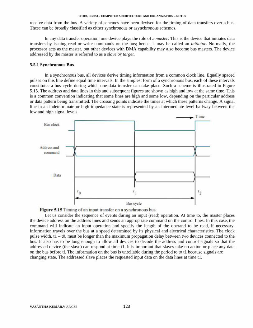
141403, CS2253 – COMPUTER ARCHITECTURE AND ORGANIZATION – NOTES
VASANTHA KUMAR.V AP/CSE 123
receive data from the bus. A variety of schemes have been devised for the timing of data transfers over a bus.These can be broadly classified as either synchronous or asynchronous schemes.
In any data transfer operation, one device plays the role of a master. This is the device that initiates datatransfers by issuing read or write commands on the bus; hence, it may be called an initiator. Normally, theprocessor acts as the master, but other devices with DMA capability may also become bus masters. The deviceaddressed by the master is referred to as a slave or target.
5.5.1 Synchronous Bus
In a synchronous bus, all devices derive timing information from a common clock line. Equally spacedpulses on this line define equal time intervals. In the simplest form of a synchronous bus, each of these intervalsconstitutes a bus cycle during which one data transfer can take place. Such a scheme is illustrated in Figure5.15. The address and data lines in this and subsequent figures are shown as high and low at the same time. Thisis a common convention indicating that some lines are high and some low, depending on the particular addressor data pattern being transmitted. The crossing points indicate the times at which these patterns change. A signalline in an indeterminate or high impedance state is represented by an intermediate level halfway between thelow and high signal levels.
Let us consider the sequence of events during an input (read) operation. At time to, the master placesthe device address on the address lines and sends an appropriate command on the control lines. In this case, thecommand will indicate an input operation and specify the length of the operand to be read, if necessary.Information travels over the bus at a speed determined by its physical and electrical characteristics. The clockpulse width, t1 – t0, must be longer than the maximum propagation delay between two devices connected to thebus. It also has to be long enough to allow all devices to decode the address and control signals so that theaddressed device (the slave) can respond at time t1. It is important that slaves take no action or place any dataon the bus before tl. The information on the bus is unreliable during the period to to t1 because signals arechanging state. The addressed slave places the requested input data on the data lines at time t1.
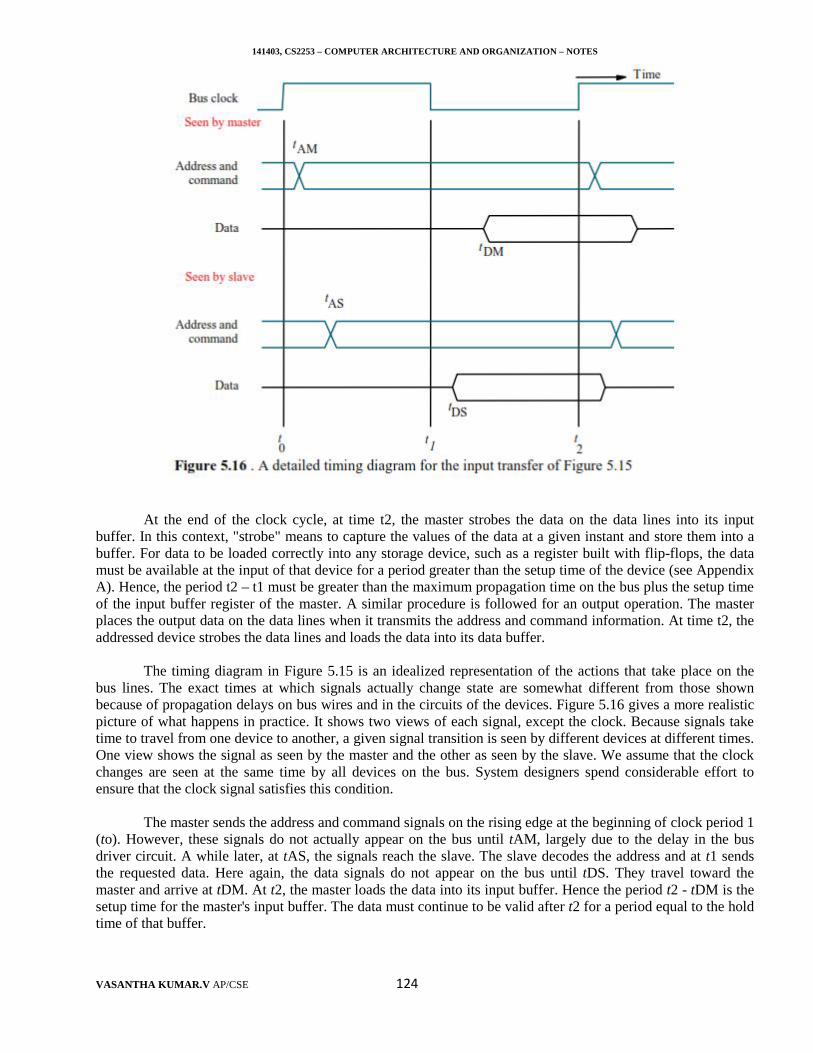
141403, CS2253 – COMPUTER ARCHITECTURE AND ORGANIZATION – NOTES
VASANTHA KUMAR.V AP/CSE 124
At the end of the clock cycle, at time t2, the master strobes the data on the data lines into its inputbuffer. In this context, "strobe" means to capture the values of the data at a given instant and store them into abuffer. For data to be loaded correctly into any storage device, such as a register built with flip-flops, the datamust be available at the input of that device for a period greater than the setup time of the device (see AppendixA). Hence, the period t2 – t1 must be greater than the maximum propagation time on the bus plus the setup timeof the input buffer register of the master. A similar procedure is followed for an output operation. The masterplaces the output data on the data lines when it transmits the address and command information. At time t2, theaddressed device strobes the data lines and loads the data into its data buffer.
The timing diagram in Figure 5.15 is an idealized representation of the actions that take place on thebus lines. The exact times at which signals actually change state are somewhat different from those shownbecause of propagation delays on bus wires and in the circuits of the devices. Figure 5.16 gives a more realisticpicture of what happens in practice. It shows two views of each signal, except the clock. Because signals taketime to travel from one device to another, a given signal transition is seen by different devices at different times.One view shows the signal as seen by the master and the other as seen by the slave. We assume that the clockchanges are seen at the same time by all devices on the bus. System designers spend considerable effort toensure that the clock signal satisfies this condition.
The master sends the address and command signals on the rising edge at the beginning of clock period 1(to). However, these signals do not actually appear on the bus until tAM, largely due to the delay in the busdriver circuit. A while later, at tAS, the signals reach the slave. The slave decodes the address and at t1 sendsthe requested data. Here again, the data signals do not appear on the bus until tDS. They travel toward themaster and arrive at tDM. At t2, the master loads the data into its input buffer. Hence the period t2 - tDM is thesetup time for the master's input buffer. The data must continue to be valid after t2 for a period equal to the holdtime of that buffer.
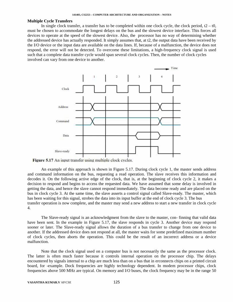
141403, CS2253 – COMPUTER ARCHITECTURE AND ORGANIZATION – NOTES
VASANTHA KUMAR.V AP/CSE 125
Multiple Cycle TransfersIn single clock transfer, a transfer has to be completed within one clock cycle, the clock period, t2 – t0,
must be chosen to accommodate the longest delays on the bus and the slowest device interface. This forces alldevices to operate at the speed of the slowest device. Also, the processor has no way of determining whetherthe addressed device has actually responded. It simply assumes that, at t2, the output data have been received bythe I/O device or the input data are available on the data lines. If, because of a malfunction, the device does notrespond, the error will not be detected. To overcome these limitations, a high-frequency clock signal is usedsuch that a complete data transfer cycle would span several clock cycles. Then, the number of clock cyclesinvolved can vary from one device to another.
An example of this approach is shown in Figure 5.17. During clock cycle 1, the master sends addressand command information on the bus, requesting a read operation. The slave receives this information anddecodes it. On the following active edge of the clock, that is, at the beginning of clock cycle 2, it makes adecision to respond and begins to access the requested data. We have assumed that some delay is involved ingetting the data, and hence the slave cannot respond immediately. The data become ready and are placed on thebus in clock cycle 3. At the same time, the slave asserts a control signal called Slave-ready. The master, whichhas been waiting for this signal, strobes the data into its input buffer at the end of clock cycle 3. The bustransfer operation is now complete, and the master may send a new address to start a new transfer in clock cycle4.
The Slave-ready signal is an acknowledgment from the slave to the master, con- finning that valid datahave been sent. In the example in Figure 5.17, the slave responds in cycle 3. Another device may respondsooner or later. The Slave-ready signal allows the duration of a bus transfer to change from one device toanother. If the addressed device does not respond at all, the master waits for some predefined maximum numberof clock cycles, then aborts the operation. This could be the result of an incorrect address or a devicemalfunction.
Note that the clock signal used on a computer bus is not necessarily the same as the processor clock.The latter is often much faster because it controls internal operation on the processor chip. The delaysencountered by signals internal to a chip are much less than on a bus that in erconnects chips on a printed circuitboard, for -example. Dock frequencies are highly technology dependent. In modem processor chips, clockfrequencies above 500 MHz are typical. On memory and I/O buses, the clock frequency may be in the range 50
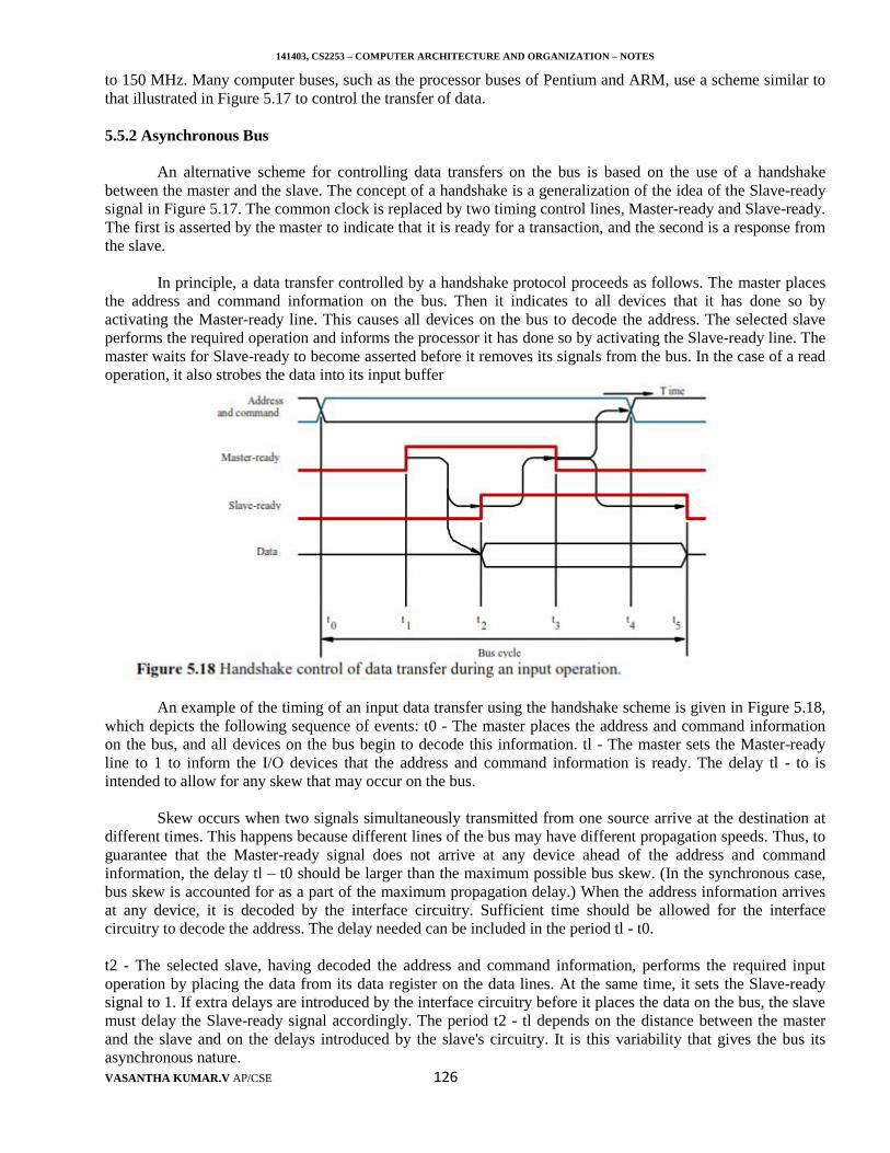
141403, CS2253 – COMPUTER ARCHITECTURE AND ORGANIZATION – NOTES
VASANTHA KUMAR.V AP/CSE 126
to 150 MHz. Many computer buses, such as the processor buses of Pentium and ARM, use a scheme similar tothat illustrated in Figure 5.17 to control the transfer of data.
5.5.2 Asynchronous Bus
An alternative scheme for controlling data transfers on the bus is based on the use of a handshakebetween the master and the slave. The concept of a handshake is a generalization of the idea of the Slave-readysignal in Figure 5.17. The common clock is replaced by two timing control lines, Master-ready and Slave-ready.The first is asserted by the master to indicate that it is ready for a transaction, and the second is a response fromthe slave.
In principle, a data transfer controlled by a handshake protocol proceeds as follows. The master placesthe address and command information on the bus. Then it indicates to all devices that it has done so byactivating the Master-ready line. This causes all devices on the bus to decode the address. The selected slaveperforms the required operation and informs the processor it has done so by activating the Slave-ready line. Themaster waits for Slave-ready to become asserted before it removes its signals from the bus. In the case of a readoperation, it also strobes the data into its input buffer
An example of the timing of an input data transfer using the handshake scheme is given in Figure 5.18,which depicts the following sequence of events: t0 - The master places the address and command informationon the bus, and all devices on the bus begin to decode this information. tl - The master sets the Master-readyline to 1 to inform the I/O devices that the address and command information is ready. The delay tl - to isintended to allow for any skew that may occur on the bus.
Skew occurs when two signals simultaneously transmitted from one source arrive at the destination atdifferent times. This happens because different lines of the bus may have different propagation speeds. Thus, toguarantee that the Master-ready signal does not arrive at any device ahead of the address and commandinformation, the delay tl – t0 should be larger than the maximum possible bus skew. (In the synchronous case,bus skew is accounted for as a part of the maximum propagation delay.) When the address information arrivesat any device, it is decoded by the interface circuitry. Sufficient time should be allowed for the interfacecircuitry to decode the address. The delay needed can be included in the period tl - t0.
t2 - The selected slave, having decoded the address and command information, performs the required inputoperation by placing the data from its data register on the data lines. At the same time, it sets the Slave-readysignal to 1. If extra delays are introduced by the interface circuitry before it places the data on the bus, the slavemust delay the Slave-ready signal accordingly. The period t2 - tl depends on the distance between the masterand the slave and on the delays introduced by the slave's circuitry. It is this variability that gives the bus itsasynchronous nature.
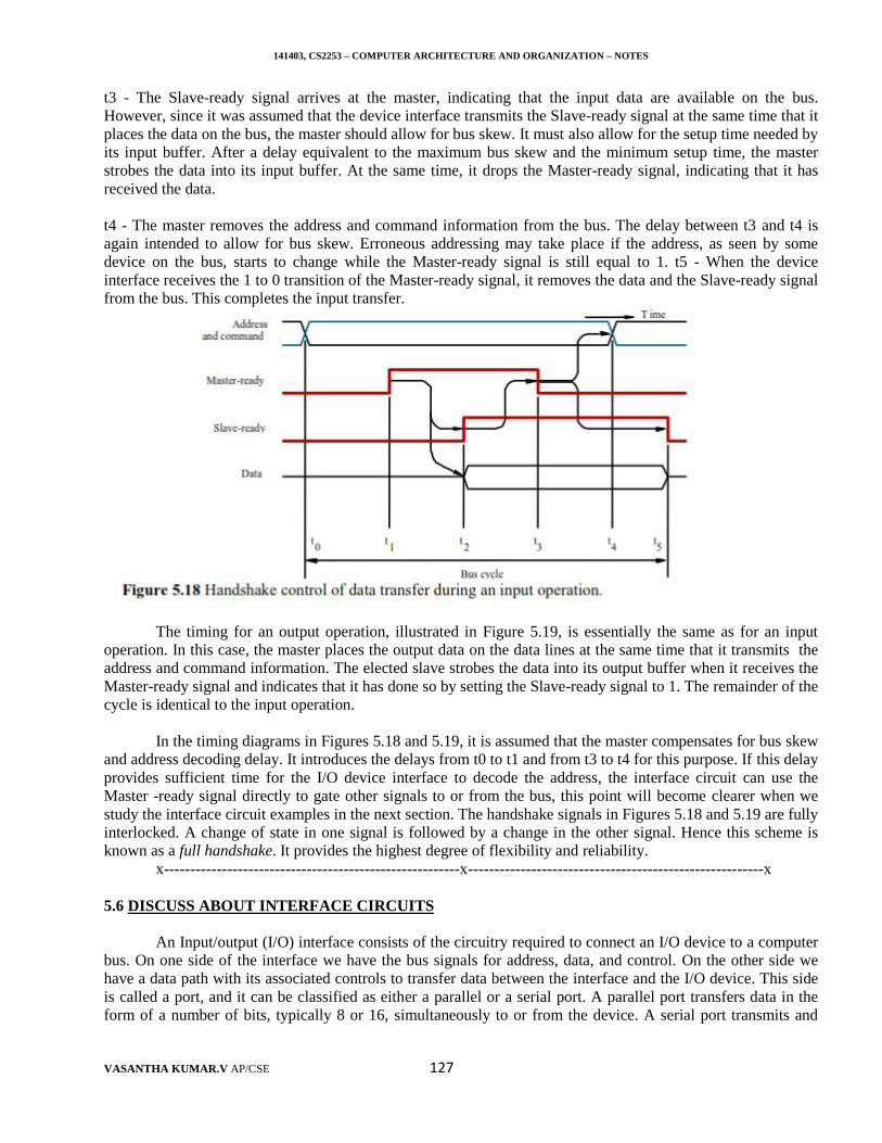
141403, CS2253 – COMPUTER ARCHITECTURE AND ORGANIZATION – NOTES
VASANTHA KUMAR.V AP/CSE 127
t3 - The Slave-ready signal arrives at the master, indicating that the input data are available on the bus.However, since it was assumed that the device interface transmits the Slave-ready signal at the same time that itplaces the data on the bus, the master should allow for bus skew. It must also allow for the setup time needed byits input buffer. After a delay equivalent to the maximum bus skew and the minimum setup time, the masterstrobes the data into its input buffer. At the same time, it drops the Master-ready signal, indicating that it hasreceived the data.
t4 - The master removes the address and command information from the bus. The delay between t3 and t4 isagain intended to allow for bus skew. Erroneous addressing may take place if the address, as seen by somedevice on the bus, starts to change while the Master-ready signal is still equal to 1. t5 - When the deviceinterface receives the 1 to 0 transition of the Master-ready signal, it removes the data and the Slave-ready signalfrom the bus. This completes the input transfer.
The timing for an output operation, illustrated in Figure 5.19, is essentially the same as for an inputoperation. In this case, the master places the output data on the data lines at the same time that it transmits theaddress and command information. The elected slave strobes the data into its output buffer when it receives theMaster-ready signal and indicates that it has done so by setting the Slave-ready signal to 1. The remainder of thecycle is identical to the input operation.
In the timing diagrams in Figures 5.18 and 5.19, it is assumed that the master compensates for bus skewand address decoding delay. It introduces the delays from t0 to t1 and from t3 to t4 for this purpose. If this delayprovides sufficient time for the I/O device interface to decode the address, the interface circuit can use theMaster -ready signal directly to gate other signals to or from the bus, this point will become clearer when westudy the interface circuit examples in the next section. The handshake signals in Figures 5.18 and 5.19 are fullyinterlocked. A change of state in one signal is followed by a change in the other signal. Hence this scheme isknown as a full handshake. It provides the highest degree of flexibility and reliability.
x--------------------------------------------------------x--------------------------------------------------------x
5.6 DISCUSS ABOUT INTERFACE CIRCUITS
An Input/output (I/O) interface consists of the circuitry required to connect an I/O device to a computerbus. On one side of the interface we have the bus signals for address, data, and control. On the other side wehave a data path with its associated controls to transfer data between the interface and the I/O device. This sideis called a port, and it can be classified as either a parallel or a serial port. A parallel port transfers data in theform of a number of bits, typically 8 or 16, simultaneously to or from the device. A serial port transmits and
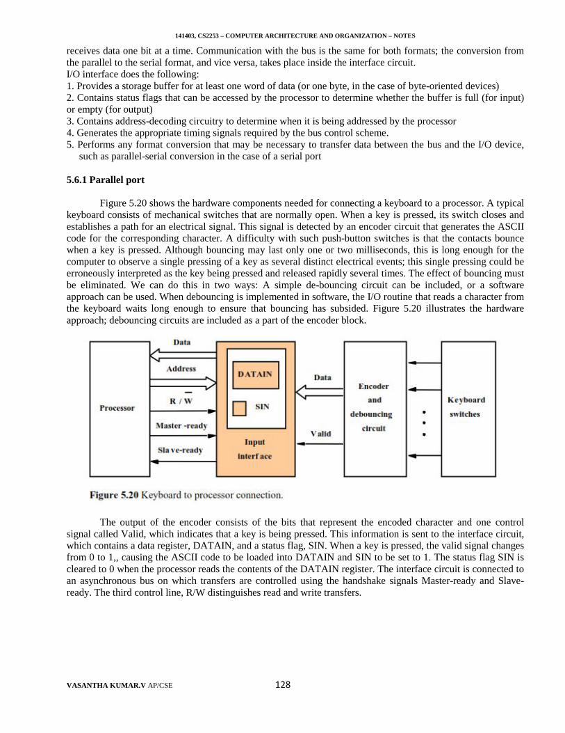
141403, CS2253 – COMPUTER ARCHITECTURE AND ORGANIZATION – NOTES
VASANTHA KUMAR.V AP/CSE 128
receives data one bit at a time. Communication with the bus is the same for both formats; the conversion fromthe parallel to the serial format, and vice versa, takes place inside the interface circuit.I/O interface does the following:1. Provides a storage buffer for at least one word of data (or one byte, in the case of byte-oriented devices)2. Contains status flags that can be accessed by the processor to determine whether the buffer is full (for input)or empty (for output)3. Contains address-decoding circuitry to determine when it is being addressed by the processor4. Generates the appropriate timing signals required by the bus control scheme.5. Performs any format conversion that may be necessary to transfer data between the bus and the I/O device,
such as parallel-serial conversion in the case of a serial port
5.6.1 Parallel port
Figure 5.20 shows the hardware components needed for connecting a keyboard to a processor. A typicalkeyboard consists of mechanical switches that are normally open. When a key is pressed, its switch closes andestablishes a path for an electrical signal. This signal is detected by an encoder circuit that generates the ASCIIcode for the corresponding character. A difficulty with such push-button switches is that the contacts bouncewhen a key is pressed. Although bouncing may last only one or two milliseconds, this is long enough for thecomputer to observe a single pressing of a key as several distinct electrical events; this single pressing could beerroneously interpreted as the key being pressed and released rapidly several times. The effect of bouncing mustbe eliminated. We can do this in two ways: A simple de-bouncing circuit can be included, or a softwareapproach can be used. When debouncing is implemented in software, the I/O routine that reads a character fromthe keyboard waits long enough to ensure that bouncing has subsided. Figure 5.20 illustrates the hardwareapproach; debouncing circuits are included as a part of the encoder block.
The output of the encoder consists of the bits that represent the encoded character and one controlsignal called Valid, which indicates that a key is being pressed. This information is sent to the interface circuit,which contains a data register, DATAIN, and a status flag, SIN. When a key is pressed, the valid signal changesfrom 0 to 1,, causing the ASCII code to be loaded into DATAIN and SIN to be set to 1. The status flag SIN iscleared to 0 when the processor reads the contents of the DATAIN register. The interface circuit is connected toan asynchronous bus on which transfers are controlled using the handshake signals Master-ready and Slave-ready. The third control line, R/W distinguishes read and write transfers.
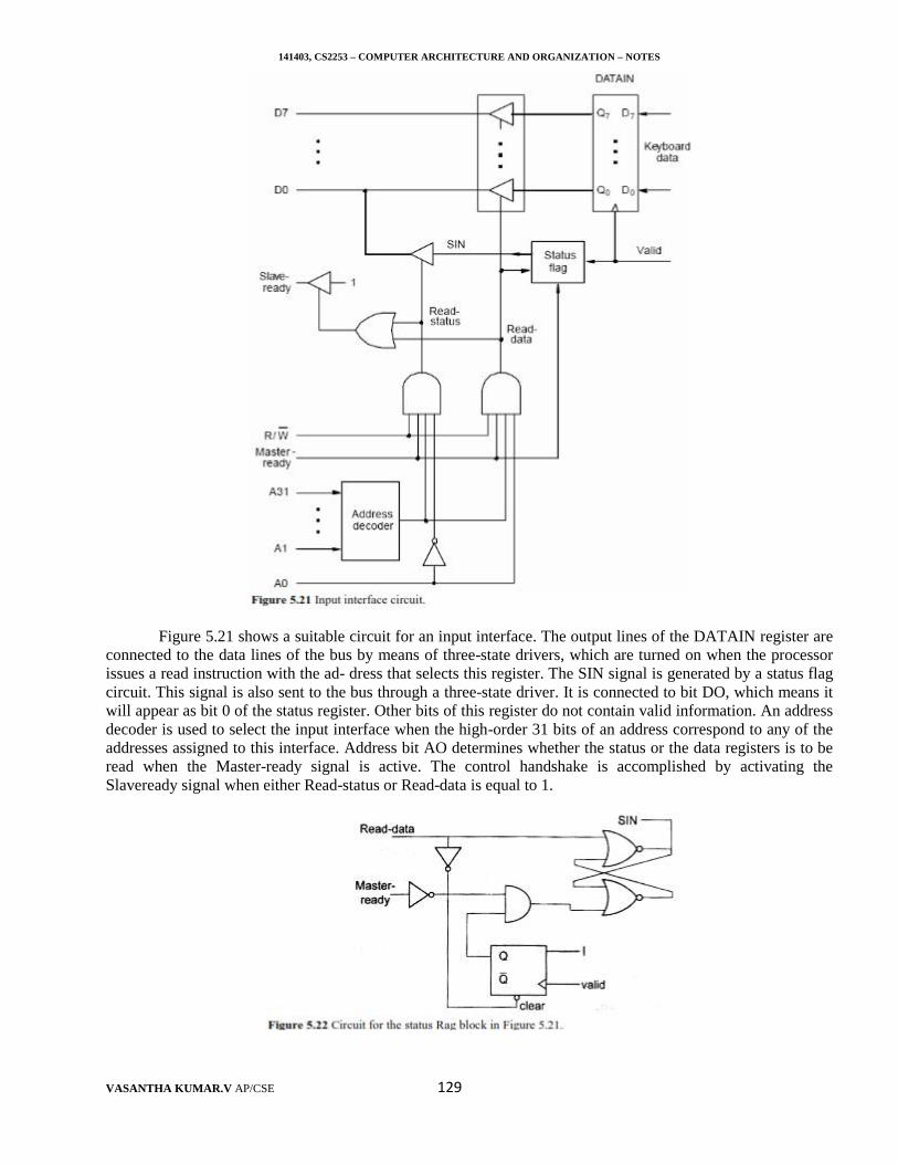
141403, CS2253 – COMPUTER ARCHITECTURE AND ORGANIZATION – NOTES
VASANTHA KUMAR.V AP/CSE 129
Figure 5.21 shows a suitable circuit for an input interface. The output lines of the DATAIN register areconnected to the data lines of the bus by means of three-state drivers, which are turned on when the processorissues a read instruction with the ad- dress that selects this register. The SIN signal is generated by a status flagcircuit. This signal is also sent to the bus through a three-state driver. It is connected to bit DO, which means itwill appear as bit 0 of the status register. Other bits of this register do not contain valid information. An addressdecoder is used to select the input interface when the high-order 31 bits of an address correspond to any of theaddresses assigned to this interface. Address bit AO determines whether the status or the data registers is to beread when the Master-ready signal is active. The control handshake is accomplished by activating theSlaveready signal when either Read-status or Read-data is equal to 1.
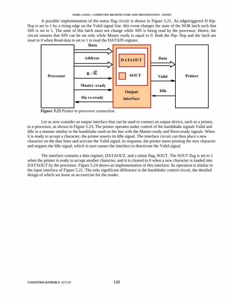
141403, CS2253 – COMPUTER ARCHITECTURE AND ORGANIZATION – NOTES
VASANTHA KUMAR.V AP/CSE 130
A possible implementation of the status flag circuit is shown in Figure 5.21. An edgetriggered D flip-flop is set to 1 by a rising edge on the Valid signal line. this event changes the state of the NOR latch such thatSIN is set to 1. The state of this latch must not change while SIN is being read by the processor. Hence, thecircuit ensures that SIN can be set only while Master ready is equal to 0. Both the flip- flop and the latch arereset to 0 when Read-data is set to 1 to read the DATAIN register.
Let us now consider an output interface that can be used to connect an output device, such as a printer,to a processor, as shown in Figure 5.23. The printer operates under control of the handshake signals Valid andIdle in a manner similar to the handshake used on the bus with the Master-ready and Slave-ready signals. Whenit is ready to accept a character, the printer asserts its Idle signal. The interface circuit can then place a newcharacter on the data lines and activate the Valid signal. In response, the printer starts printing the new characterand negates the Idle signal, which in turn causes the interface to deactivate the Valid signal.
The interface contains a data register, DATAOUT, and a status flag, SOUT. The SOUT flag is set to 1when the printer is ready to accept another character, and it is cleared to 0 when a new character is loaded intoDATAOUT by the processor. Figure 5.24 shows an implementation of this interface. Its operation is similar tothe input interface of Figure 5.21. The only significant difference is the handshake control circuit, the detaileddesign of which we leave as an exercise for the reader.
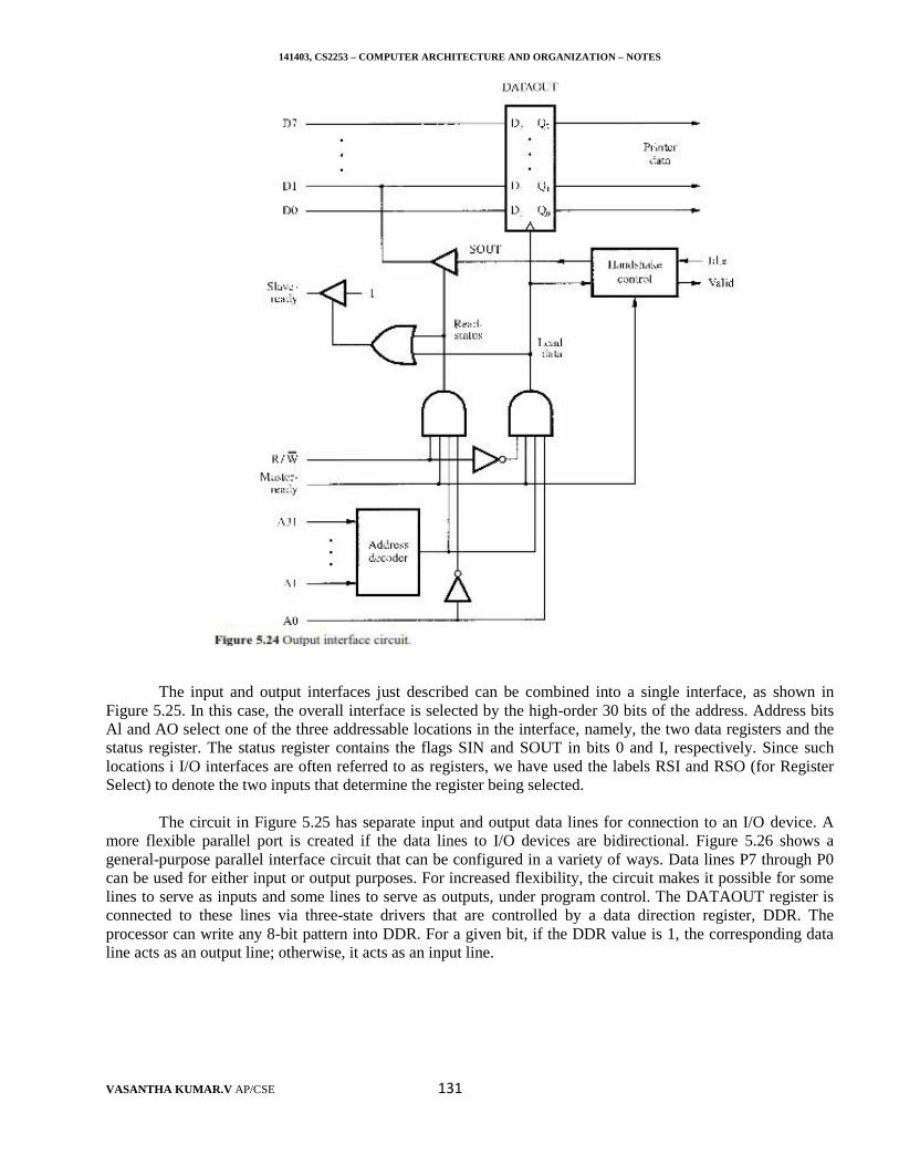
141403, CS2253 – COMPUTER ARCHITECTURE AND ORGANIZATION – NOTES
VASANTHA KUMAR.V AP/CSE 131
The input and output interfaces just described can be combined into a single interface, as shown inFigure 5.25. In this case, the overall interface is selected by the high-order 30 bits of the address. Address bitsAl and AO select one of the three addressable locations in the interface, namely, the two data registers and thestatus register. The status register contains the flags SIN and SOUT in bits 0 and I, respectively. Since suchlocations i I/O interfaces are often referred to as registers, we have used the labels RSI and RSO (for RegisterSelect) to denote the two inputs that determine the register being selected.
The circuit in Figure 5.25 has separate input and output data lines for connection to an I/O device. Amore flexible parallel port is created if the data lines to I/O devices are bidirectional. Figure 5.26 shows ageneral-purpose parallel interface circuit that can be configured in a variety of ways. Data lines P7 through P0can be used for either input or output purposes. For increased flexibility, the circuit makes it possible for somelines to serve as inputs and some lines to serve as outputs, under program control. The DATAOUT register isconnected to these lines via three-state drivers that are controlled by a data direction register, DDR. Theprocessor can write any 8-bit pattern into DDR. For a given bit, if the DDR value is 1, the corresponding dataline acts as an output line; otherwise, it acts as an input line.
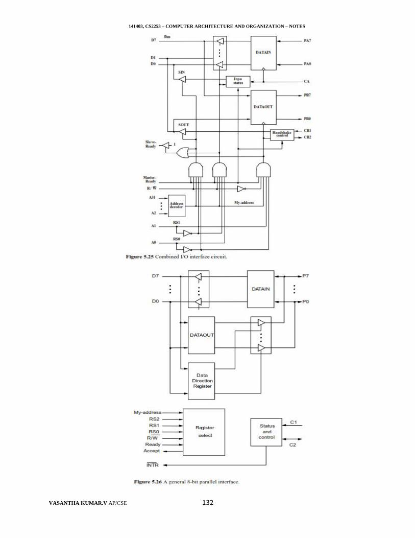
141403, CS2253 – COMPUTER ARCHITECTURE AND ORGANIZATION – NOTES
VASANTHA KUMAR.V AP/CSE 132
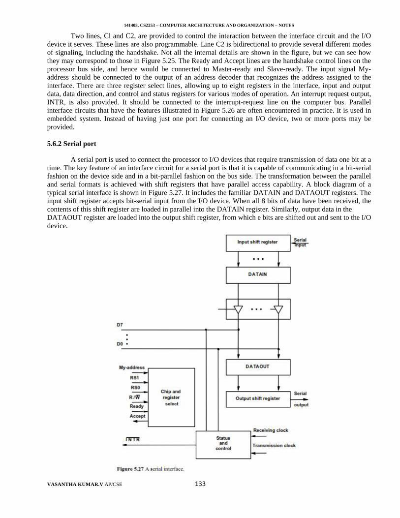
141403, CS2253 – COMPUTER ARCHITECTURE AND ORGANIZATION – NOTES
VASANTHA KUMAR.V AP/CSE 133
Two lines, Cl and C2, are provided to control the interaction between the interface circuit and the I/Odevice it serves. These lines are also programmable. Line C2 is bidirectional to provide several different modesof signaling, including the handshake. Not all the internal details are shown in the figure, but we can see howthey may correspond to those in Figure 5.25. The Ready and Accept lines are the handshake control lines on theprocessor bus side, and hence would be connected to Master-ready and Slave-ready. The input signal My-address should be connected to the output of an address decoder that recognizes the address assigned to theinterface. There are three register select lines, allowing up to eight registers in the interface, input and outputdata, data direction, and control and status registers for various modes of operation. An interrupt request output,INTR, is also provided. It should be connected to the interrupt-request line on the computer bus. Parallelinterface circuits that have the features illustrated in Figure 5.26 are often encountered in practice. It is used inembedded system. Instead of having just one port for connecting an I/O device, two or more ports may beprovided.
5.6.2 Serial port
A serial port is used to connect the processor to I/O devices that require transmission of data one bit at atime. The key feature of an interface circuit for a serial port is that it is capable of communicating in a bit-serialfashion on the device side and in a bit-parallel fashion on the bus side. The transformation between the paralleland serial formats is achieved with shift registers that have parallel access capability. A block diagram of atypical serial interface is shown in Figure 5.27. It includes the familiar DATAIN and DATAOUT registers. Theinput shift register accepts bit-serial input from the I/O device. When all 8 bits of data have been received, thecontents of this shift register are loaded in parallel into the DATAIN register. Similarly, output data in theDATAOUT register are loaded into the output shift register, from which e bits are shifted out and sent to the I/Odevice.
141403, CS2253 – COMPUTER ARCHITECTURE AND ORGANIZATION – NOTES
VASANTHA KUMAR.V AP/CSE 134
The part of the interface that deals with the bus is the same as in the parallel interface described earlier.The status flags SIN and SOUT serve similar functions. The SIN flag is set to 1when new data are loaded inDATAIN; it is cleared to 0 when the processor reads the contents of DATAIN. As soon as the data aretransferred from the input shift register into the DATAIN register, the shift register can start accepting the next8-bit character from the I/O device. The SOUT flag indicates whether the output buffer is available. It is clearedto 0 when the processor writes new data into the DATAOUT register and set to 1 when data are transferredfrom DATAOUT into the output shift register.
The double buffering used in the input and output paths are important. A simpler interface could beimplemented by turning DATAIN and DATA OUT into shift registers and eliminating the shift registers inFigure 5.27. However, this would impose awkward restrictions on the operation of the I/O device; afterreceiving one character from the serial line, the device cannot start receiving the next character until theprocessor reads the contents of DATAIN. Thus, a pause would be needed between two characters to allow theprocessor to read the input data. With the double buffer, the transfer of the second character can begin as soonas the first character is loaded from the shift register into the DATAIN register. Thus, provided the processorreads the contents of DATAIN before the serial transfer of the second character is completed, the interface canreceive a continuo us stream of serial data. An analogous situation occurs in the output path of theinterface.
Because it requires fewer wires, serial transmission is convenient for connecting devices that arephysically far away from the computer. The speed of transmission, often given as a bit rate, depends on thenature of the devices connected. To accommodate a range of devices, a serial interface must be able to use arange of clock speeds. The circuit in Figure 5.27 allows separate clock signals to be used for input and outputoperations for increased flexibility. Because serial interfaces play a vital role in connecting I/O devices, severalwidely used standards have been developed. A standard circuit that includes the features of our example inFigure 5.27 is known as a Universal Asynchronous Receiver Transmitter (UART). It is intended for use withlow-speed serial devices. Data transmission is performed using the asynchronous start-stop format. To facilitateconnection to communication links, a popular standard known as RS-232-C was developed.
x--------------------------------------------------------x--------------------------------------------------------x
5.7 DESCRIBE ABOUT STANDARD I/O INTERFACE
A number of standards have been developed for I/O Interface. IBM developed a they called ISA(Industry Standard Architecture) for their personal computer known at the time as PC AT. The popularity ofthat computer led to other manufacturers producing ISA –compatible interfaces for their 110 devices, thusmaking ISA into a de facto standard. Some standards have been developed through industrial cooperativeefforts, even among competing companies driven by their common self-interest in having compatible products.In some cases, organizations such as the IEEE (Institute of Electrical and Electronics Engineers), ANSI(American Nationa1 Standards Institute), or international bodies such as ISO (International StandardsOrganization) have blessed these standards and given them an official status.
There are three widely used bus standards, PCI (Peripheral Component Interconnect), SCSI (SmallComputer System Interface), and USB (Universal Serial Bus). The way these standards are used in a typicalcomputer system is illustrated in Figure 5.28. The PCI standard defines an expansion bus on the motherboard.SCSI and USB are used for connecting additional devices, both inside and outside the computer box. The SCSIbus is a high-speed parallel bus intended for devices such as disks and video displays. The USB bus uses serialtransmission to suit the needs of equipment ranging from keyboards to game controls to internet connections.The figure shows an interface circuit that enables devices compatible with the earlier ISA standard, such as thepopular IDE (Integrated Device Electronics) disk, to be connected. It also shows a connection to an Ethernet.The Ethernet is a widely used local area network, providing a high-speed connection among computers in abuilding or a university campus. A given computer may use more than one bus standard. A typical Pentiumcomputer has both a PCI bus and an ISA bus, thus providing the user with a wide range of devices to choosefrom.
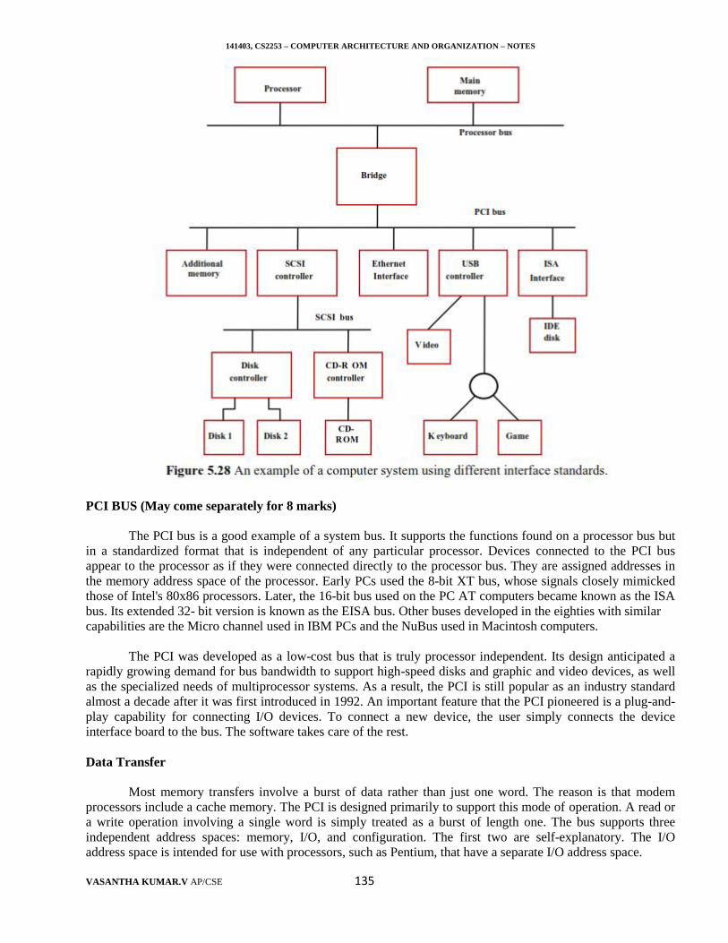
141403, CS2253 – COMPUTER ARCHITECTURE AND ORGANIZATION – NOTES
VASANTHA KUMAR.V AP/CSE 135
PCI BUS (May come separately for 8 marks)
The PCI bus is a good example of a system bus. It supports the functions found on a processor bus butin a standardized format that is independent of any particular processor. Devices connected to the PCI busappear to the processor as if they were connected directly to the processor bus. They are assigned addresses inthe memory address space of the processor. Early PCs used the 8-bit XT bus, whose signals closely mimickedthose of Intel's 80x86 processors. Later, the 16-bit bus used on the PC AT computers became known as the ISAbus. Its extended 32- bit version is known as the EISA bus. Other buses developed in the eighties with similarcapabilities are the Micro channel used in IBM PCs and the NuBus used in Macintosh computers.
The PCI was developed as a low-cost bus that is truly processor independent. Its design anticipated arapidly growing demand for bus bandwidth to support high-speed disks and graphic and video devices, as wellas the specialized needs of multiprocessor systems. As a result, the PCI is still popular as an industry standardalmost a decade after it was first introduced in 1992. An important feature that the PCI pioneered is a plug-and-play capability for connecting I/O devices. To connect a new device, the user simply connects the deviceinterface board to the bus. The software takes care of the rest.
Data Transfer
Most memory transfers involve a burst of data rather than just one word. The reason is that modemprocessors include a cache memory. The PCI is designed primarily to support this mode of operation. A read ora write operation involving a single word is simply treated as a burst of length one. The bus supports threeindependent address spaces: memory, I/O, and configuration. The first two are self-explanatory. The I/Oaddress space is intended for use with processors, such as Pentium, that have a separate I/O address space.
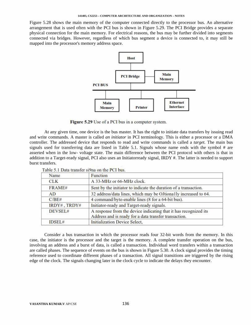
141403, CS2253 – COMPUTER ARCHITECTURE AND ORGANIZATION – NOTES
VASANTHA KUMAR.V AP/CSE 136
Figure 5.28 shows the main memory of the computer connected directly to the processor bus. An alternativearrangement that is used often with the PCI bus is shown in Figure 5.29. The PCI Bridge provides a separatephysical connection for the main memory. For electrical reasons, the bus may be further divided into segmentsconnected via bridges. However, regardless of which bus segment a device is connected to, it may still bemapped into the processor's memory address space.
At any given time, one device is the bus master. It has the right to initiate data transfers by issuing readand write commands. A master is called an initiator in PCI terminology. This is either a processor or a DMAcontroller. The addressed device that responds to read and write commands is called a target. The main bussignals used for transferring data are listed in Table 5.1. Signals whose name ends with the symbol # areasserted when in the low- voltage state. The main difference between the PCI protocol with others is that inaddition to a Target-ready signal, PCI also uses an Initiatorready signal, IRDY #. The latter is needed to supportburst transfers.
Consider a bus transaction in which the processor reads four 32-bit words from the memory. In thiscase, the initiator is the processor and the target is the memory. A complete transfer operation on the bus,involving an address and a burst of data, is called a transaction. Individual word transfers within a transactionare called phases. The sequence of events on the bus is shown in Figure 5.30. A clock signal provides the timingreference used to coordinate different phases of a transaction. All signal transitions are triggered by the risingedge of the clock. The signals changing later in the clock cycle to indicate the delays they encounter.
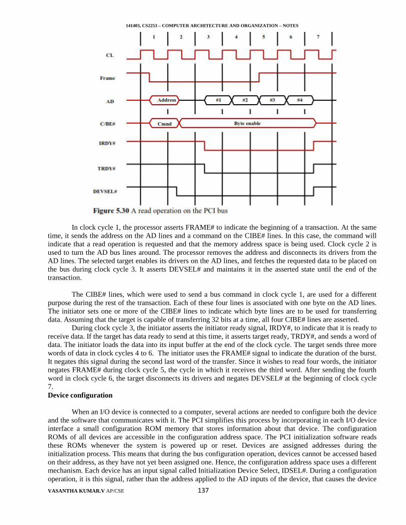
141403, CS2253 – COMPUTER ARCHITECTURE AND ORGANIZATION – NOTES
VASANTHA KUMAR.V AP/CSE 137
In clock cycle 1, the processor asserts FRAME# to indicate the beginning of a transaction. At the sametime, it sends the address on the AD lines and a command on the CIBE# lines. In this case, the command willindicate that a read operation is requested and that the memory address space is being used. Clock cycle 2 isused to turn the AD bus lines around. The processor removes the address and disconnects its drivers from theAD lines. The selected target enables its drivers on the AD lines, and fetches the requested data to be placed onthe bus during clock cycle 3. It asserts DEVSEL# and maintains it in the asserted state until the end of thetransaction.
The CIBE# lines, which were used to send a bus command in clock cycle 1, are used for a differentpurpose during the rest of the transaction. Each of these four lines is associated with one byte on the AD lines.The initiator sets one or more of the CIBE# lines to indicate which byte lines are to be used for transferringdata. Assuming that the target is capable of transferring 32 bits at a time, all four CIBE# lines are asserted.
During clock cycle 3, the initiator asserts the initiator ready signal, IRDY#, to indicate that it is ready toreceive data. If the target has data ready to send at this time, it asserts target ready, TRDY#, and sends a word ofdata. The initiator loads the data into its input buffer at the end of the clock cycle. The target sends three morewords of data in clock cycles 4 to 6. The initiator uses the FRAME# signal to indicate the duration of the burst.It negates this signal during the second last word of the transfer. Since it wishes to read four words, the initiatornegates FRAME# during clock cycle 5, the cycle in which it receives the third word. After sending the fourthword in clock cycle 6, the target disconnects its drivers and negates DEVSEL# at the beginning of clock cycle7.Device configuration
When an I/O device is connected to a computer, several actions are needed to configure both the deviceand the software that communicates with it. The PCI simplifies this process by incorporating in each I/O deviceinterface a small configuration ROM memory that stores information about that device. The configurationROMs of all devices are accessible in the configuration address space. The PCI initialization software readsthese ROMs whenever the system is powered up or reset. Devices are assigned addresses during theinitialization process. This means that during the bus configuration operation, devices cannot be accessed basedon their address, as they have not yet been assigned one. Hence, the configuration address space uses a differentmechanism. Each device has an input signal called Initialization Device Select, IDSEL#. During a configurationoperation, it is this signal, rather than the address applied to the AD inputs of the device, that causes the device
141403, CS2253 – COMPUTER ARCHITECTURE AND ORGANIZATION – NOTES
VASANTHA KUMAR.V AP/CSE 138
to be selected. The motherboard in which device connectors are plugged typically has the IDSEL# pin of eachdevice connected to one of the upper 21 address lines, AD 11 to AD31. Hence, a device can be selected for aconfiguration operation by issuing a configuration command and an address in which the corresponding ADline is set to 1 and the remaining 20 lines set to O. The lower address lines, ADI0 to ADOO, are used to specifythe type of operation and to access the contents of the device configuration ROM. This arrangement limits thenumber of 110 devices to 21.
The configuration software scans all 21 locations in the configuration address space to identify whichdevices are present. Each device may request an address in the I/O space or in the memory space. The device isthen assigned an address by writing that address into the appropriate device register. The configuration softwarealso sets such parameters as the device interrupt priority. The PCI bus has four interrupt-request lines. Bywriting into a device configuration register, the software instructs the device as to which of these lines it can useto request an interrupt. If a device requires initialization, the initialization code is stored in a ROM in the deviceinterface. (This is a different ROM from that used in the configuration process.) The PCI software reads thiscode and executes it to perform the required initialization.
This process relieves the user from having to be involved in the configuration process. The user simplyplugs in the interface board and turns on the power. The software does the rest. The device is ready to use. ThePCI bus has gained great popularity in the PC world. It is also used in many other computers, such as SUNs, tobenefit from the wide range of 110 devices for which a PCI interface is available. In the case of someprocessors, such as the Compaq Alpha, the PCI-processor bridge circuit is built on the processor chip itself,further simplifying system design and packaging.
Electrical Characteristics
The PCI bus has been defined for operation with either a 5- or 3.3- V power supply. The motherboardmay be designed to operate with either signaling system. Connectors on expansion boards are designed toensure that they can be plugged only in a compatible motherboard.
5.7.2 SCSI (Small Computer System Interface) (May come separately for 8 marks)
The acronym SCSI stands for Small Computer System Interface. It refers to a standard bus defined bythe American National Standards Institute (ANSI) under the designation X3.131. In the original specificationsof the standard, devices such as disks are connected to a computer via a 50- wire cable, which can be up to 25meters in length and can transfer data at rates up to 5 megabytes/s. The SCSI bus standard has undergone manyrevisions, and its data transfer capability has increased very rapidly, almost doubling every two years. SCSI-2and SCSI-3 have been defined, and each has several options.
A SCSI bus may have eight data lines, in which case it is called a narrow bus and transfers data onebyte at a time. Because of these various options, the SCSI connector may have 50, 68, or 80 pins. Themaximum transfer rate in commercial devices that are currently available varies from 5 megabytes/s to 160megabytes/so The most recent version of the standard is intended to support transfer rates up to 320megabytes/s, and 640 megabytes/s is anticipated a little later. Devices connected to the SCSI bus are not part ofthe address space of the processor in the same way as devices connected to the processor bus. The SCSI bus isconnected to the processor bus through a SCSI controller, as shown in Figure 5.28. This controller uses DMA totransfer data packets from the main memory to the device, or vice versa. A packet may contain a block of data,commands from the processor to the device, or status information about the device.
A controller connected to a SCSI bus is one of two types - an initiator or a target. An initiator has theability to select a particular target and to send commands specifying the operations to be performed. The diskcontroller operates as a target. It carries out the commands it receives from the initiator. The initiator establishesa logical connection with the intended target. Once this connection has been established, it can be suspendedand restored as needed to transfer commands and bursts of data. While a particular connection is suspended,
141403, CS2253 – COMPUTER ARCHITECTURE AND ORGANIZATION – NOTES
VASANTHA KUMAR.V AP/CSE 139
other devices can use the bus to transfer information. This ability to overlap data transfer requests is one of thekey features of the SCSI bus that leads to its high performance.
Data transfers on the SCSI bus are always controlled by the target controller. To send a command to atarget, an initiator requests control of the bus and, after winning arbitration, selects the controller it wants tocommunicate with and hands control of the bus over to it. Then the controller starts a data transfer operation toreceive a command from the initiator. Assume that the processor wishes to read a block of data from a diskdrive and that these data are stored in two disk sectors that are not contiguous. The processor sends a commandto the SCSI controller, which causes the following sequence of events to take place:
1. The SCSI controller, acting as an initiator, contends for control of the bus.2. When the 'initiator wins the arbitration process, it selects the target controller and hands over control of thebus to it.3. The target starts an output operation (from initiator to target); in response to this, the initiator sends acommand specifying the required read operation.4. The target, realizing that it first needs to perform a disk seek operation, sends a message to the initiatorindicating that it will temporarily suspend the connection between them. Then it releases the bus.5. The target controller sends a command to the disk drive to move the read head to the first sector involved inthe requested read operation. Then, it reads the data stored in that sector and stores them in a data buffer. Whenit is ready to begin transferring data to the initiator, the target requests control of the bus. After it winsarbitration, it res elects the initiator controller, thus restoring the suspended connection.6. The target transfers the contents of the data buffer to the initiator and then suspends the connection again.Data are transferred either 8 or 16 bits in parallel, depending on the width of the bus.7. The target controller sends a command to the disk drive to perform another seek operation. Then, it transfersthe contents of the second disk sector to the initiator, as before. At the end of this transfer, the logicalconnection between the two controllers is terminated.8. As the initiator controller receives the data, it stores them into the main memory using the DMA approach.9. The SCSI controller sends an interrupt to the processor to inform it that the requested operation has beencompleted.
This scenario shows that the messages exchanged over the SCSI bus are at a higher level than thoseexchanged over the processor bus. The SCSI bus standard defines a wide range of control messages that can beex- changed between the controllers to handle different types of I/O devices. Messages are also defined to dealwith various error or failure conditions that might arise during device operation or data transfer.
Bus SignalThe bus signals are summarized in Table 5.2. For simplicity we show the signals for a narrow bus (8
data lines). Note that all signal names are preceded by a minus sign. This indicates that the signals are active, orthat a data line is equal to 1, when they are in the low-voltage state. The bus has no address lines. Instead, thedata lines are used to identify the bus controllers involved during the selection or reselection process and duringbus arbitration. For a narrow bus, there are eight possible controllers, numbered o through 7, and each i,associated with the data line that has the same number. A wide bus accommodates up to 16 controllers. Acontroller places its own address or the address of another controller on the bus by activating the correspondingdata line. Thus, it is possible to have more than one address on the bus at the same time, as in the arbitrationprocess we describe next. Once a connection is established between two controllers, there is no further need foraddressing, and the data lines are used to carry data.
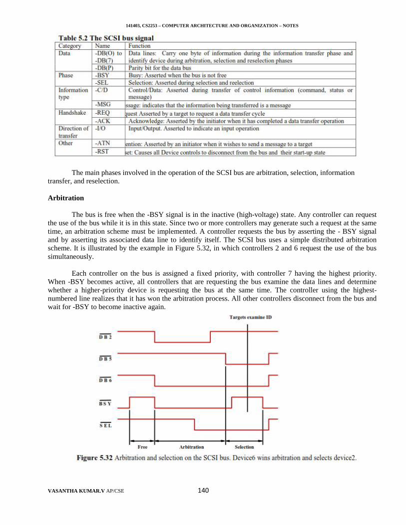
141403, CS2253 – COMPUTER ARCHITECTURE AND ORGANIZATION – NOTES
VASANTHA KUMAR.V AP/CSE 140
The main phases involved in the operation of the SCSI bus are arbitration, selection, informationtransfer, and reselection.
Arbitration
The bus is free when the -BSY signal is in the inactive (high-voltage) state. Any controller can requestthe use of the bus while it is in this state. Since two or more controllers may generate such a request at the sametime, an arbitration scheme must be implemented. A controller requests the bus by asserting the - BSY signaland by asserting its associated data line to identify itself. The SCSI bus uses a simple distributed arbitrationscheme. It is illustrated by the example in Figure 5.32, in which controllers 2 and 6 request the use of the bussimultaneously.
Each controller on the bus is assigned a fixed priority, with controller 7 having the highest priority.When -BSY becomes active, all controllers that are requesting the bus examine the data lines and determinewhether a higher-priority device is requesting the bus at the same time. The controller using the highest-numbered line realizes that it has won the arbitration process. All other controllers disconnect from the bus andwait for -BSY to become inactive again.
141403, CS2253 – COMPUTER ARCHITECTURE AND ORGANIZATION – NOTES
VASANTHA KUMAR.V AP/CSE 141
In Figure 5.32, we have assumed that controller 6 is an initiator that wishes to establish a connection tocontroller 5. After winning arbitration, controller 6 proceeds to the selection phase, in which it identifies thetarget.
Selection
Having won arbitration, controller 6 continues to assert -BSY and -DB6 (its address). It indicates that itwishes to select controller 5 by asserting the -SEL and then the - DB5 lines. Any other controller that may havebeen involved in the arbitration phase, such as controller 2 in the figure, must stop driving the data lines oncethe -SEL line becomes active, if it has not already done so. After placing the address of the target controller onthe bus, the initiator releases the –BSY line. The selected target controller responds by asserting - BSY. Thisinforms the initiator that the connection it is requesting has been established, so that it may remove the addressinformation from the data lines. The selection process is now complete, and the target controller (controller 5)is asserting - BSY. From this point on, controller 5 has control of the bus, as required for theinformation transfer phase.
Information Transfer
The information transferred between two controllers may consist of commands from the initiator to thetarget, status responses from the target to the initiator, or data being transferred to or from the I/O device.Handshake signaling is used to control information transfers. The - REQ and - ACK signals replace the Master-ready and Slave-ready signals. The target asserts - I/O during an input operation (target to initiator), and itasserts -CID to indicate that the information being transferred is a command or a status response rather thandata.
High-speed versions of the SCSI bus use a technique known as double-edge clocking or DoubleTransitions (DT). Each data transfer requires a high-to-low transition followed by a lowto- high transition onthe two handshake signals. Double-edge clocking means that data are transferred on both the rising and fallingedges of these signals, thus doubling the transfer rate. At the end of the transfer, the target controller releases the- BSY signal, thus freeing the bus for use by other devices.
Reselection
When a logical connection is suspended and the target is ready to restore it, the target must first gaincontrol of the bus. It starts an arbitration cycle, and after winning arbitration, it selects the initiator controller inexactly the same manner as described above. But with the roles of the target and initiator reversed, the initiatoris now asserting - BSY. Before data transfer can begin, the initiator must hand control over to the target. This isachieved by having the target controller assert - BSY r selecting the initiator. Meanwhile, the initiator waits fora short period after being selected to make sure that the target has asserted -BS and then it releases the -BSYline. The connection between the two controllers has now been reestablished, with the target in control of thebus as required for data transfer to proceed.
The bus signaling scheme described above provides the mechanisms needed for two controllers toestablish a logical connection and exchange messages. The connection may be suspended and reestablished atany time. The SCSI standard defines the structure and contents of various types of packets that the controllersexchange to handle different situations. The initiator uses these packets to send the commands it receives fromthe processor to the target. The target responds with status information and data transfer operations. The latterare controlled by the target, because it is the target that knows when data are available, when to suspend andreestablish connections, etc.
5.7.3 USB (Universal Serial Bus). (May come separately for 8 marks)
Universal Serial Bus (USB) is an industry standard developed through a collaborative effort of severalcomputer and communications companies, including Compaq, Hewlett-Packard, Intel, Lucent, Microsoft,
141403, CS2253 – COMPUTER ARCHITECTURE AND ORGANIZATION – NOTES
VASANTHA KUMAR.V AP/CSE 142
Nortel Networks, and Philips. USB is a simple and low cost mechanism to connect the devices such askeyboards, mouse, cameras, speakers, printer and display devices to the computer.
The USB supports two speeds of operation, called low-speed (1.5 megabits/s) and fullspeed (12megabits/s). The most recent revision of the bus specification (USB 2.0) introduced a third speed of operation,called high-speed (480 megabits/s). The USB is quickly gaining acceptance in the market place, and with theaddition of the high-speed capability it may well become the interconnection method of choice for mostcomputer devices. The USB has been designed to meet several key objectives:
· Provide a simple, low-cost, and easy to use interconnection system that overcomes the difficulties due to thelimited number of I/O ports available on a computer· Accommodate a wide range of data transfer characteristics for I/O devices, including telephone and Internetconnections· Enhance user convenience through a "plug-and-play" mode of operation
Port limitation
Only a few ports are provided in a typical computer. To add new ports, a user must open the computerbox to gain access to the internal expansion bus and install a new interface card. The user may also need toknow how to configure the device and the software. An objective of the USB is to make it possible to add manydevices to a computer system at any time, without opening the computer box.
Device Characteristics
The different kinds of devices may be connected to a computer cover a wide range of functionality. Thespeed, volume, and timing constraints associated with data transfers to and from such devices vary significantly.In the case of a keyboard, one byte of data is generated every time a key is pressed, which may happen at anytime. These data should be transferred to the computer promptly. Since the event of pressing a key is notsynchronized to any other event in -8 computer system, the data generated by the keyboard are calledasynchronous. Furthermore, the rate at which the data are generated is quite low. It is limited by the speed ofthe human operator to about 100 bytes per second, which is less than 1000 bits per second.
Let us consider a different source of data. Many computers have a microphone either externallyattached or built in. The sound picked up by the microphone produces an analog electrical signal, which must beconverted into a digital form before it can be handled by the computer. This is accomplished by sampling theanalog signal periodically. For each sample, an analog-to-digital (A/D) converter generates an n-bit numberrepresenting the magnitude of the sample. The number of bits, n, is selected based on, the desired precision withwhich to represent each sample. Later, when these data are sent to a speaker, a digital-to-analog (D/A) converteris used to restore the original analog signal from the digital format. The sampling process yields a continuousstream of digitized samples that arrive at regular intervals, synchronized with the sampling clock. Such a datastream is called isochronous, meaning that successive events are separated by equal periods of time.
Plug-and-play
The plug-and-play feature means that a new device, such as an additional speaker, can be connected atany time while the system is operating. The system should detect the existence of this new device automatically,identify the appropriate device-driver soft- ware and any other facilities needed to service that device, andestablish the appropriate addresses and logical connections to enable them to communicate. The plug-and-playrequirement has many implications at all levels in the system, from the hardware to the operating system andthe applications software. One of the primary objectives of the design of the USB has been to provide a plug-and-play capability.
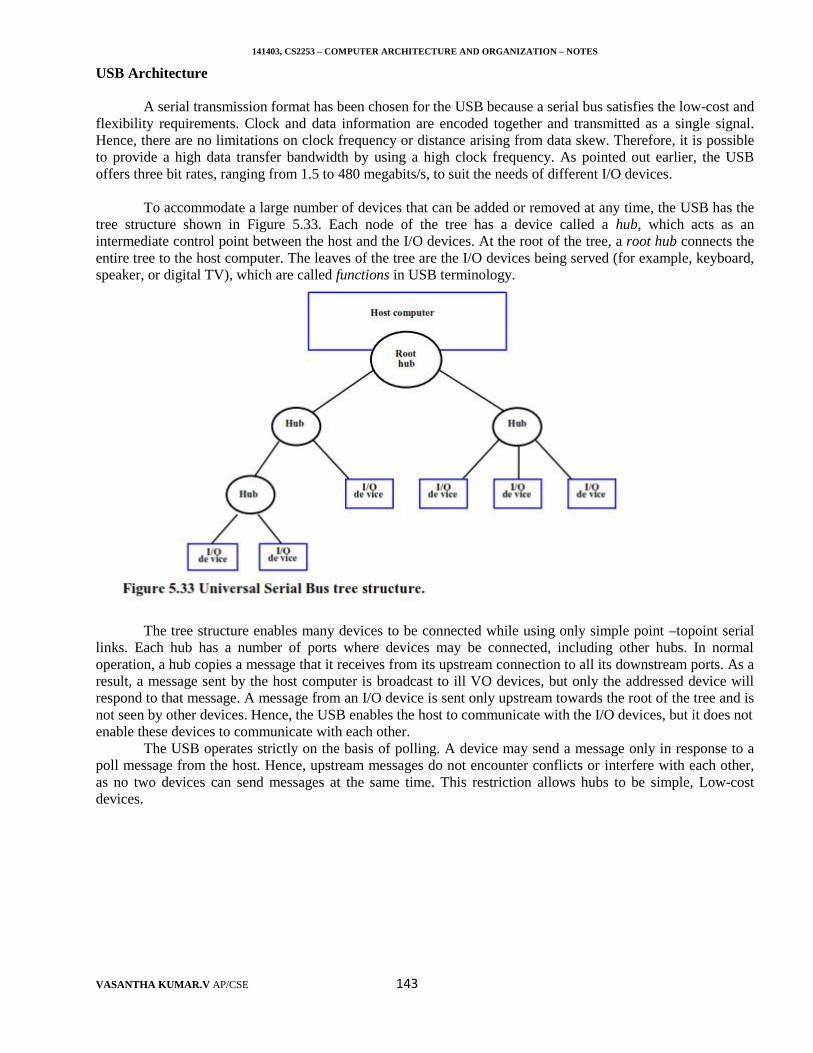
141403, CS2253 – COMPUTER ARCHITECTURE AND ORGANIZATION – NOTES
VASANTHA KUMAR.V AP/CSE 143
USB Architecture
A serial transmission format has been chosen for the USB because a serial bus satisfies the low-cost andflexibility requirements. Clock and data information are encoded together and transmitted as a single signal.Hence, there are no limitations on clock frequency or distance arising from data skew. Therefore, it is possibleto provide a high data transfer bandwidth by using a high clock frequency. As pointed out earlier, the USBoffers three bit rates, ranging from 1.5 to 480 megabits/s, to suit the needs of different I/O devices.
To accommodate a large number of devices that can be added or removed at any time, the USB has thetree structure shown in Figure 5.33. Each node of the tree has a device called a hub, which acts as anintermediate control point between the host and the I/O devices. At the root of the tree, a root hub connects theentire tree to the host computer. The leaves of the tree are the I/O devices being served (for example, keyboard,speaker, or digital TV), which are called functions in USB terminology.
The tree structure enables many devices to be connected while using only simple point –topoint seriallinks. Each hub has a number of ports where devices may be connected, including other hubs. In normaloperation, a hub copies a message that it receives from its upstream connection to all its downstream ports. As aresult, a message sent by the host computer is broadcast to ill VO devices, but only the addressed device willrespond to that message. A message from an I/O device is sent only upstream towards the root of the tree and isnot seen by other devices. Hence, the USB enables the host to communicate with the I/O devices, but it does notenable these devices to communicate with each other.
The USB operates strictly on the basis of polling. A device may send a message only in response to apoll message from the host. Hence, upstream messages do not encounter conflicts or interfere with each other,as no two devices can send messages at the same time. This restriction allows hubs to be simple, Low-costdevices.
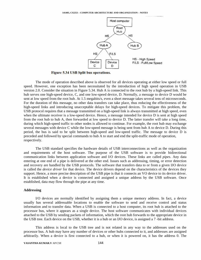
141403, CS2253 – COMPUTER ARCHITECTURE AND ORGANIZATION – NOTES
VASANTHA KUMAR.V AP/CSE 144
The mode of operation described above is observed for all devices operating at either low speed or fullspeed. However, one exception has been necessitated by the introduction of high speed operation in USBversion 2.0. Consider the situation in Figure 5.34. Hub A is connected to the root hub by a high-speed link. Thishub serves one high-speed device, C, and one low-speed device, D. Normally, a message to device D would besent at low speed from the root hub. At 1.5 megabits/s, even a short message takes several tens of microseconds.For the duration of this message, no other data transfers can take place, thus reducing the effectiveness of thehigh-speed links and introducing unacceptable delays for high-speed devices. To mitigate this problem, theUSB protocol requires that a message transmitted on a high-speed link is always transmitted at high speed, evenwhen the ultimate receiver is a low-speed device. Hence, a message intended for device D is sent at high speedfrom the root hub to hub A, then forwarded at low speed to device D. The latter transfer will take a long time,during which high-speed traffic to other nodes is allowed to continue. For example, the root hub may exchangeseveral messages with device C while the low-speed message is being sent from hub A to device D. During thisperiod, the bus is said to be split between high-speed and low-speed traffic. The message to device D ispreceded and followed by special commands to hub A to start and end the split-traffic mode of operation,respectively.
The USB standard specifies the hardware details of USB interconnections as well as the organizationand requirements of the host software. The purpose of the USB software is to provide bidirectionalcommunication links between application software and I/O devices. These links are called pipes. Any dataentering at one end of a pipe is delivered at the other end. Issues such as addressing, timing, or error detectionand recovery are handled by the USB protocols. The software that transfers data to or from a given IJO deviceis called the device driver for that device. The device drivers depend on the characteristics of the devices theysupport. Hence, a more precise description of the USB pipe is that it connects an VO device to its device driver.It is established when a device is connected and assigned a unique address by the USB software. Onceestablished, data may flow through the pipe at any time.
Addressing
I/O devices are normally identified by assigning them a unique memory address. In fact, a deviceusually has several addressable locations to enable the software to send and receive control and statusinformation and to transfer data. When a USB is connected to a host computer, its root hub is attached to theprocessor bus, where it appears as a single device. The host software communicates with individual devicesattached to the USB by sending packets of information, which the root hub forwards to the appropriate device inthe USB tree. Each device on the USB, whether it is a hub or an IJO device, is assigned a 7 -bit address.
This address is local to the USB tree and is not related in any way to the addresses used on theprocessor bus. A hub may have any number of devices or other hubs connected to it, and addresses are assignedarbitrarily. When a device is first connected to a hub, or when it is powered on, it has the address 0. The
141403, CS2253 – COMPUTER ARCHITECTURE AND ORGANIZATION – NOTES
VASANTHA KUMAR.V AP/CSE 145
hardware of the hub to which this device is connected is capable of detecting that the device has beenconnected, and it records this fact as part of its own status information. Periodically, the host polls each hub tocollect status information and learn about new devices that may have been added or disconnected.
USB Protocol
All information transferred over the USB is organized in packets, where a packet consists of one ormore bytes of information. There are many types of packets that perform a variety of control functions. Theinformation transferred on the USB can be divided into two broad categories: control and data. Control packetsperform such tasks as addressing a device to initiate data transfer, acknowledging that data have been receivedcorrectly, or indicating an error. Data packets carry information that is delivered to a device. For example, putand output data are transferred inside data packets.
A packet consists of one or more fields containing different kinds of information. The first field of anypacket is called the packet identifier, PID, which identifies the type of that packet. There are four bits ofinformation in this field, but they are transmitted twice. The first time they are sent with their true values, andthe second time with each bit complemented, as shown in Figure 5.35(a). This enables the receiving device toverify that the PID byte has been received correctly.
The four PID bits identify one of 16 different packet types. Some control packets, such as ACK(Acknowledge), consist only of the PID byte. Control packets used for controlling data transfer operations arecalled token packets. They have the format shown in Figure 5.35(b). A token packet starts with the PID field,using one of two PID values to distinguish between an IN packet and an OUT packet, which control input andoutput transfers, respectively. The PID field is followed by the 7 -bit address of a device and the 4-bit endpointnumber within that device. The packet ends with 5 bits for error checking, using a method called cyclicredundancy check (CRC). The CRC bits are computed based on the contents of the address and endpoint fields.By performing an inverse computation, the receiving device can determine whether the packet has beenreceived correctly.
Data packets, which carry input and output data, have the format shown in Figure 4.45c. The packetidentifier field is followed by up to 8192 bits of data, then 16 error-checking bits. Three different PID patternsare used to identify data packets, so that data packets may be numbered 0, 1, or 2. Note that data packets do not
141403, CS2253 – COMPUTER ARCHITECTURE AND ORGANIZATION – NOTES
VASANTHA KUMAR.V AP/CSE 146
carry a device address or an endpoint number. This information is included in the IN or OUT token packet thatinitiates the transfer.
Consider an output device connected to a USB hub, which in turn is connected to a host computer. Anexample of an output operation is shown in Figure 5.36. The host computer sends a token packet of type OUTto the hub, followed by a data packet containing the output data. The PID field of the data packet identifies it asdata packet number o. The hub verifies that the transmission has been error free by checking the error controlbits, and then sends an acknowledgment packet (ACK) back to the host. The hub forwards the token and datapackets downstream. All I/O devices receive this sequence of packets, but only the device that recognizesits address in the token packet accepts the data in the packet that follows. After verifying that transmission hasbeen error free, it sends an ACK packet to the hub.
Successive data packets on a full-speed or low-speed pipe carry the numbers 0 and 1, alternately. Thissimplifies recovery from transmission errors. If a token, data, or acknowledgment packet is lost as a result of atransmission error, the sender resends the entire sequence. By checking the data packet number in the PID field,the receiver can detect and discard duplicate packets. High-speed data packets are sequentially numbered 0, 1,2, 0, and so on. Input operations follow a similar procedure. The host sends a token packet of type IN containingthe device address. In effect, this packet is a poll asking the device to send any input data it may have. Thedevice responds by sending a data packet followed by an ACK. If it has no data ready, it responds by sending anegative acknowledgment (NAK) instead.
Electrical characteristics
The cables used for USB connections consist of four wires. Two are used to carry power, +5 V andGround. Thus, a hub or an I/O device may be powered directly from the bus, or it may have its own externalpower connection. The other two wires are used to carry data. Different signaling schemes are used for differentspeeds of transmission. At low speed, 1s and 0s are transmitted by sending a high voltage state (5 V) on one orthe other of the two signal wires. For high-speed links, differential transmission is used.
x--------------------------------------------------------x--------------------------------------------------------x
141403, CS2253 – COMPUTER ARCHITECTURE AND ORGANIZATION – NOTES
VASANTHA KUMAR.V AP/CSE 147
5.8. DISCUSS ABOUT I/O DEVICE
Keyboard:The computer keyboard is used to enter text information into the computer, as when you type the
contents of a report. The keyboard can also be used to type commands directing the computer to perform certainactions. In addition to the keys of the main keyboard (used for typing text), keyboards usually also have anumeric keypad (for entering numerical data efficiently), a bank of editing keys (used in text editingoperations), and a row of function keys along the top (to easily invoke certain program functions). Laptopcomputers, which don’t have room for large keyboards, often include a “fn” key so that other keys can performdouble duty (such as having a numeric keypad function embedded within the main keyboard keys).
Mouse:
The mouse pointing device sits on your work surface and is moved with your hand. In older mice, a ballin the bottom of the mouse rolls on the surface as you move the mouse, and internal rollers sense the ballmovement and transmit the information to the computer via the cord of the mouse. The newer optical mousedoes not use a rolling ball, but instead uses a light and a small optical sensor to detect the motion of the mouseby tracking a tiny image of the desk surface. Optical mice avoid the problem of a dirty mouse ball, which causesregular mice to roll unsmoothly if the mouse ball and internal rollers are not cleaned frequently.
Scanners:A scanner is a device that images a printed page or graphic by digitizing it, producing an image made of
tiny pixels of different brightness and color values which are represented numerically and sent to the computer.Scanners scan graphics, but they can also scan pages of text which are then run through OCR (Optical CharacterRecognition) software that identifies the individual letter shapes and creates a text file of the page's contents.
Monitors: CRT (Cathode Ray Tube), LCD (Liquid Crystal Display)
Printers: Laser Printer, Inkjet Printer, Dot matrix printer.
x--------------------------------------------------------x--------------------------------------------------------x
141403, CS2253 – COMPUTER ARCHITECTURE AND ORGANIZATION – NOTES
VASANTHA KUMAR.V AP/CSE 148
TWO MARK QUESTIONS AND ANSWERS
UNIT – I – BASIC STRUCTURE OF COMPUTERS
1. What are the basic functional units of a computer?
A computer consist of five functionally independent main parts namely,(i) Input Unit,(ii) Memory Unit,(iii) Arithmetic and Logic Unit,(iv) Output Unit, and(v) Control Unit.
2. Define RAM.
Memory in which any location can be reached in a short and fixed amount of time after specifying itsaddress is called random access memory.
3. Define memory access time.
The time required to access one word is called memory access time.
4. What is Instruction Register (IR) and Program Counter (PC) used for?
The Instruction Register (IR) holds the instruction that is currently being executed. Its output isavailable to the control circuits which generated the timing signals that control the various processing elements.The Program Counter (PC) issued to keep rack of the execution of the program. It contains the memory addressof the next instruction to be fetched and executed.
5. What do you mean by Memory Address Register (MAR) and memory Data Register (MDR)?
The MAR holds the address of the location to be accessed. The MDR contains the data to be written into or readout of the addressed location.
6. What is an interrupt?
An interrupt is a request from an I/O device for service by the processor. The processor provides therequested service by executing an appropriate interrupt service routine.
7. Explain about Bus.
Bus is group of lines that serves as a connecting path for several devices. it, addition to the lines thatcarry the data, the bus must have the lines for address and control purposes.
8. What do you mean by multiprogramming or multitasking?
The operating system manages the concurrent execution of severe application programs to make bestpossible use of computer resources. This pattern of concurrent execution is called multiprogramming ormultitasking.
9. Give the basic performance equation.
The basic performance equation is given as T = N x S / R
141403, CS2253 – COMPUTER ARCHITECTURE AND ORGANIZATION – NOTES
VASANTHA KUMAR.V AP/CSE 149
T = It is the processor time required to execute a program.N = It is the actual number of instruction executions.S = It is average number of basic steps needs to execute one machine instruction.R = It is the clock rate
10. Explain the concept of pipelining.
Pipelining is the means of executing machine instructions concurrently. It is the effective way oforganizing concurrent activity in a computer system. It is a process of substantial improvement in theperformance by overlapping the execution of successive instructions.
11. What are the two techniques used to increase the clock rate R?
The two techniques used to increase the clock rate R are:(i) The Integrated Circuit (1C) technology can be increased which reduces the time needed to complete a basicstep.(ii) We can reduce the amount of processing done in one basic step.
12. What is Big-Endian and Little-Endian representations.
The big-endian is used when lower byte addresses are used for the more significant bytes(The leftmost bytes) of the word. The little-endian is used for the opposite ordering, where the lower byteaddresses are used for the less significant bytes (the rightmost bytes) of the word.
13. What is addressing mode?
The addressing mode is defined as the different ways in which the location of an operand is specified in aninstruction.
14. What are the different types of addressing modes available?
The different types of addressing modes available are:(i)Immediate addressing mode, (ii)Register addressing mode, (iii)Direct or absolute addressing mode,(iv)Indirect addressing mode, (v)Indexed addressing mode, (vi) Relative addressing mode,(vii)Autoincrement, and (viii) Autodecrement.
15. What is indirect addressing mode?
The effective address of the operand is the contents of a register or memory location whose addressappears in the instruction.
16. What is indexed addressing mode?
The effective address of the operand is generated by adding a constant value to the contents ofa register.
17. Define autoincrement mode of addressing.
The effective address of the operand is the contents of a register specified in the instruction. Afteraccessing the operand, the contents of this register are automatically incremented to point to the next item in thelist.18. Define autodecrement mode of addressing.
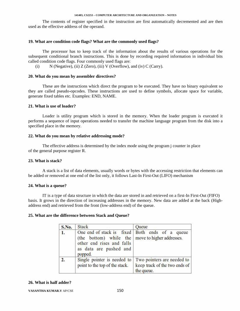
141403, CS2253 – COMPUTER ARCHITECTURE AND ORGANIZATION – NOTES
VASANTHA KUMAR.V AP/CSE 150
The contents of register specified in the instruction are first automatically decremented and are thenused as the effective address of the operand.
19. What are condition code flags? What are the commonly used flags?
The processor has to keep track of the information about the results of various operations for thesubsequent conditional branch instructions. This is done by recording required information in individual bitscalled condition code flags. Four commonly used flags are:
(i) N (Negative), (ii) Z (Zero), (iii) V (Overflow), and (iv) C (Carry).
20. What do you mean by assembler directives?
These are the instructions which direct the program to be executed. They have no binary equivalent sothey are called pseudo-opcodes. These instructions are used to define symbols, allocate space for variable,generate fixed tables etc. Examples: END, NAME.
21. What is use of loader?
Loader is utility program which is stored in the memory. When the loader program is executed itperforms a sequence of input operations needed to transfer the machine language program from the disk into aspecified place in the memory.
22. What do you mean by relative addressing mode?
The effective address is determined by the index mode using the program j counter in placeof the general purpose register R.
23. What is stack?
A stack is a list of data elements, usually words or bytes with the accessing restriction that elements canbe added or removed at one end of the list only, it follows Last-In First-Out (LIFO) mechanism
24. What is a queue?
IT is a type of data structure in which the data are stored in and retrieved on a first-In First-Out (FIFO)basis. It grows in the direction of increasing addresses in the memory. New data are added at the back (High-address end) and retrieved from the front (low-address end) of the queue.
25. What are the difference between Stack and Queue?
26. What is half adder?
141403, CS2253 – COMPUTER ARCHITECTURE AND ORGANIZATION – NOTES
VASANTHA KUMAR.V AP/CSE 151
A half adder is a logic circuit with two inputs and two outputs, which adds two bits at a time,producing a sum and a carry.
27. What is full adder?
A full adder is logic circuit with three inputs and two outputs, which adds three bits at a timegiving a sum and a carry.
28. What is signed binary?
A system in which the leading bit represents the sign and the remaining bits the magnitude ofthe number is called signed binary. This is also known as sign magnitude.
29. What are the two approaches used to reduce delay in address?
(i) The first approach is to use the fastest possible electronic technology in implementing theripple-carry logic design.(ii) The second approach is to use an augmented logic gate network structure.
30. What is a carry look - ahead adder?
The input carry needed by a stage is directly computed from carry signals obtained from all thepreceding stages i-1, i-2, ... 0, rather than waiting for normal carries to supply slowly from stage to stage. Anadder that uses this principle ii t called carry look-ahead adder.
32. How can we speed up the multiplication process?
There are two techniques to speed up the multiplication process:(i) The first technique guarantees that the maximum number of summands that must be added isn/2 for n-bit operands.(ii) The second technique reduces the time needed to add the summands.
33. What is bit pair recoding? Give an example.
Bit pair receding halves the maximum number of summands. Group the Booth-recoded multiplierbits in pairs and observe the following: the pair (+1 -1) is equivalent to the pair (0 +1). That is instead of adding-1 times the multiplicand m at shift position i to +1 x M at position i+1, the same result is obtained by adding +1x M at position i. Example: 11010 - Bit pair receding value is 0 - 1 - 2.
34. What are the two methods of achieving the 2's complement?
(i) Take the 1's complement of the number and addl.(ii) Leave all least significant O's and the first unchanged and then complement the remaining bits.
35. What are the advantages / features of using Booth algorithm?
(i) It handles both positive and negative multiplier uniformly.(ii) It achieves efficiency in the number of additions required when the multiplier has afew large blocks of 1 's.(iii) The speed gained by skipping 1 's depends on the data.
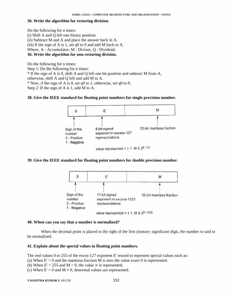
141403, CS2253 – COMPUTER ARCHITECTURE AND ORGANIZATION – NOTES
VASANTHA KUMAR.V AP/CSE 152
36. Write the algorithm for restoring division.
Do the following for n times:(i) Shift A and Q left one binary position.(ii) Subtract M and A and place the answer back in A.(iii) If the sign of A is 1, set q0 to 0 and add M back to A.Where, A - Accumulator, M - Divisor, Q - Dividend.36. Write the algorithm for non restoring division.
Do the following for n times:Step 1: Do the following for n times:* If the sign of A is 0, shift A and Q left one bit position and subtract M from A,otherwise, shift A and Q left and add M to A.* Now, if the sign of A is 0, set q0 to 1, otherwise, set q0 to 0.Step 2: If the sign of A is 1, add M to A.
38. Give the IEEE standard for floating point numbers for single precision number.
39. Give the IEEE standard for floating point numbers for double precision number.
40. When can you say that a number is normalized?
When the decimal point is placed to the right of the first (nonzer; significant digit, the number is said tobe normalized.
41. Explain about the special values in floating point numbers.
The end values 0 to 255 of the exces-127 exponent E' reused to represent special values such as:(a) When E' = 0 and the mantissa fraction M is zero the value exact 0 is represented.(b) When E' = 255 and M = 0, the value ∞ is represented.(c) When E' = 0 and M ≠ 0, denormal values are represented.
141403, CS2253 – COMPUTER ARCHITECTURE AND ORGANIZATION – NOTES
VASANTHA KUMAR.V AP/CSE 153
(d) When E' = 2555 and M ≠ 0, the value represented is called a Not a number.
42. Write the add subtract rule for floating point numbers.
(i) Choose the number with the smaller exponent and shift its mantissa right a number of stepsequal to the difference in exponents.(ii) Set the exponent of the result equal to the larger exponent.(iii) Perform addition/subtraction on the mantissa and determine the sign of the result.(iv) Normalize the resulting value, if necessary.43. Write the multiply rule for floating point numbers.
i) Add the exponent and subtract 127.ii) Multiply the mantissa and determine the sign of the result.(iii) Normalize the resulting value, if necessary.
44. What is guard bit?
Although the mantissa of initial operands is limited to 24bits, it is important to retain extra bits, calledas guard bits.
45. What are the ways to truncate the guard bits?
There are several ways to truncate the guard bits:(i) Chopping,(ii) Von Neumann rounding, and(iii) Rounding.
46. Define Carry Save Addition (CSA) process.
Instead of letting the carries ripple along the rows, they can be saved and introduced into the next row atthe correct weighted position. Delay in CSA is less than delay through the ripple carry adder.
47. What is generate and propagate function?
The generate function is given by Gi = Xi Vi andThe propagate function is given as Pi = xi + yi
48. What is excess -127format?
Instead of the signed exponent E, the value actually stored in the exponent field is and unsigned inter E'= E + 127. This format is called excess-127.
49. What is floating point numbers?
In some cases, the binary point is variable and is automatically adjusted as computation proceeds. Insuch case, the binary point is said to float and the numbers are called floating point numbers.
50. In floating point numbers when so you say that an underflow or overflow has occurred?
In single precision numbers when an exponent is less than - 126 then we say that an underflow hasoccurred. In single precision numbers when an exponent is less than +127 then we say that an overflow hasoccurred.
UNIT – II – BASIC PROCESSING UNIT
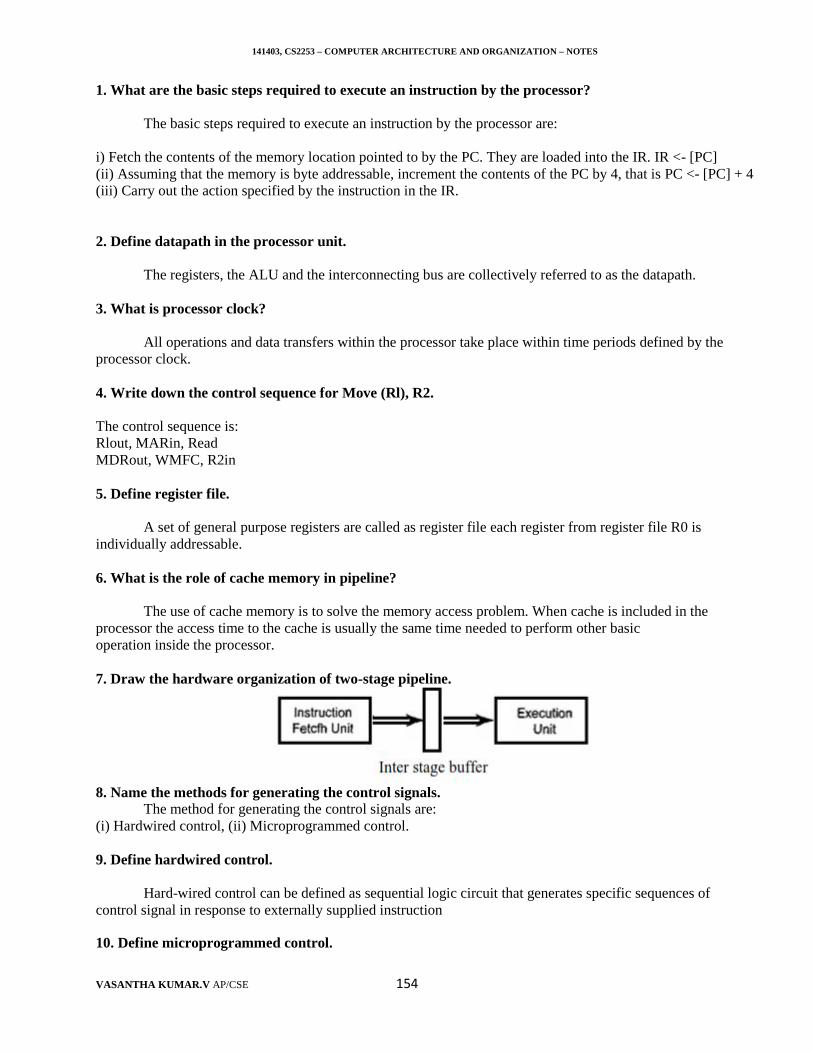
141403, CS2253 – COMPUTER ARCHITECTURE AND ORGANIZATION – NOTES
VASANTHA KUMAR.V AP/CSE 154
1. What are the basic steps required to execute an instruction by the processor?
The basic steps required to execute an instruction by the processor are:
i) Fetch the contents of the memory location pointed to by the PC. They are loaded into the IR. IR <- [PC](ii) Assuming that the memory is byte addressable, increment the contents of the PC by 4, that is PC <- [PC] + 4(iii) Carry out the action specified by the instruction in the IR.
2. Define datapath in the processor unit.
The registers, the ALU and the interconnecting bus are collectively referred to as the datapath.
3. What is processor clock?
All operations and data transfers within the processor take place within time periods defined by theprocessor clock.
4. Write down the control sequence for Move (Rl), R2.
The control sequence is:Rlout, MARin, ReadMDRout, WMFC, R2in
5. Define register file.
A set of general purpose registers are called as register file each register from register file R0 isindividually addressable.
6. What is the role of cache memory in pipeline?
The use of cache memory is to solve the memory access problem. When cache is included in theprocessor the access time to the cache is usually the same time needed to perform other basicoperation inside the processor.
7. Draw the hardware organization of two-stage pipeline.
8. Name the methods for generating the control signals.The method for generating the control signals are:
(i) Hardwired control, (ii) Microprogrammed control.
9. Define hardwired control.
Hard-wired control can be defined as sequential logic circuit that generates specific sequences ofcontrol signal in response to externally supplied instruction
10. Define microprogrammed control.
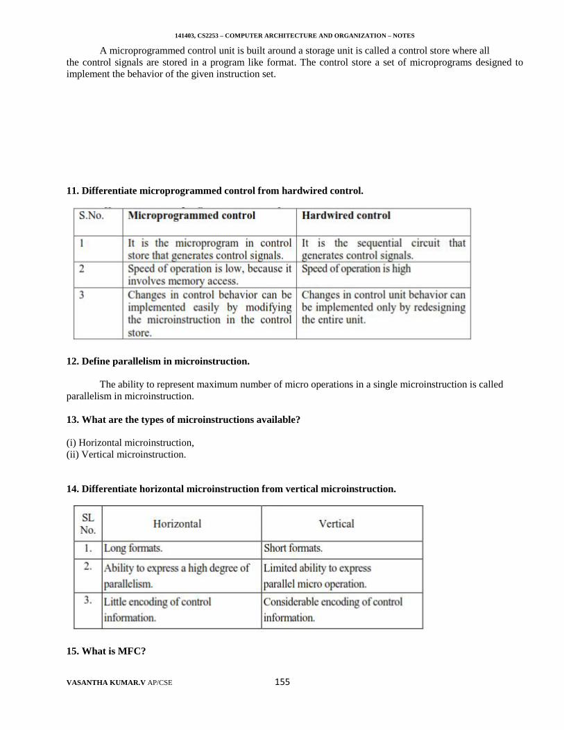
141403, CS2253 – COMPUTER ARCHITECTURE AND ORGANIZATION – NOTES
VASANTHA KUMAR.V AP/CSE 155
A microprogrammed control unit is built around a storage unit is called a control store where allthe control signals are stored in a program like format. The control store a set of microprograms designed toimplement the behavior of the given instruction set.
11. Differentiate microprogrammed control from hardwired control.
12. Define parallelism in microinstruction.
The ability to represent maximum number of micro operations in a single microinstruction is calledparallelism in microinstruction.
13. What are the types of microinstructions available?
(i) Horizontal microinstruction,(ii) Vertical microinstruction.
14. Differentiate horizontal microinstruction from vertical microinstruction.
15. What is MFC?
141403, CS2253 – COMPUTER ARCHITECTURE AND ORGANIZATION – NOTES
VASANTHA KUMAR.V AP/CSE 156
To accommodate the variability in response time, the processor waits until it receives an indication thatthe requested read operation has been completed. This is accomplished by a control signal called Memory-Function-Completed.
UNIT – III – PIPELINING
1. What are the major characteristics of a pipeline?
The major characteristics of a pipeline are:(i) Pipelining cannot be implemented on a single task, as if works by splitting multiple tasks into a number ofsubtasks and operating on them simultaneously.(ii) The speedup or efficiency achieved by using a pipeline depends on the number of pipe stages and thenumber of available tasks that can be subdivided.(iii) If the task that can be subdivided has uneven length of execution times, then the speedup of the pipeline isreduced.(iv) Though the pipeline architecture does not reduce the time of execution of a single task, it reduces theoverall time taken for the entire job to get completed.
2. What is a pipeline hazard?
Any condition that causes the pipeline to stall is called hazard. They are also called as stalls orbubbles.
3. What are the types of pipeline hazards?
The various pipeline hazards are:(i) Data hazard, (ii) Structural Hazard, and (iii) Control Hazard.
4. What is data hazard?
Any condition in which either the source or the destination operand of an instruction are notavailable at the time expected in the pipeline is called data hazard.
5. What is instruction or control hazard?
The pipeline may be stalled because of a delay in the availability of an instruction. Forexample, this may be a result of a miss in the cache, requiring the instruction to be fetched from themain memory. Such hazards are often called control hazards or instruction hazard.
6. Define structural hazards.
This is the situation when two instruction require the use of a given hardware resource atthe same time. The most common case in which this hazard may arise is in access to memory.
7. What is side effect?
When a location other than one explicitly named in an instruction as a destinationoperand is affected, the instruction is said to have a side effect.
8. What do you mean by branch penalty?
The time lost as a result of a branch instruction is often referred to as branch penalty.
9. What is branch folding?
141403, CS2253 – COMPUTER ARCHITECTURE AND ORGANIZATION – NOTES
VASANTHA KUMAR.V AP/CSE 157
When the instruction fetch unit executes the branch instruction concurrently with theexecution of the other instruction, then this technique is called branch folding.
10. What do you mean by delayed branching?
Delayed branching is used to minimize the penalty incurred as a result of conditional branch instruction.The location following the branch instruction is called delay slot. The instructions in the delay slots are alwaysfetched and they are arranged such that they are fully executed whether or not branch is taken. That is branchingtakes place one instruction later than where the branch instruction appears in the instruction sequence in thememory hence the name delayed branching.
11. What are the two types of branch prediction techniques available?
The two types of branch prediction techniques are,(I) Static branch prediction, (II) Dynamic branch prediction
UNIT – IV – MEMORY SYSTEM
1. Define Memory Access Time.
It is the time taken by the memory to supply the contents of a location, from the time, itreceives "READ".
2. Define memory cycle time.
It is defined as the minimum time delay required between the initiations of two successivememory operations.
3. What is RAM?
This storage location can be accessed in any order and access time is independent of thelocation being accessed.
4. What is cache memory?
It is a fast memory that is inserted between the larger slower main memory and the processor.It holds the currently active segments of a program and their data.
5. Explain virtual memory.
The data is to be stored in physical memory locations that have addresses different from thosespecified by the program. The memory control circuitry translates the address specified by the program into anaddress that can be used to access the physical memory.
6. List the various semiconductors RAMs.
(i) Static RAM, and(ii) Dynamic RAM.
7. What do you mean by static memories?
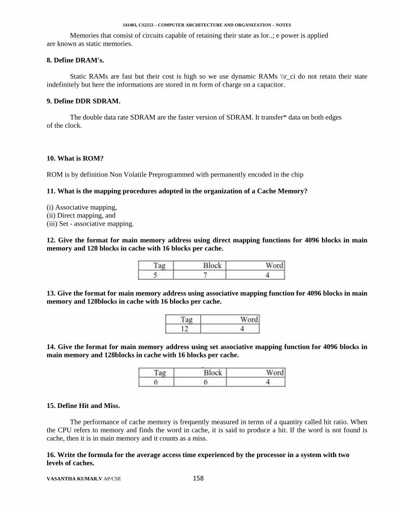
141403, CS2253 – COMPUTER ARCHITECTURE AND ORGANIZATION – NOTES
VASANTHA KUMAR.V AP/CSE 158
Memories that consist of circuits capable of retaining their state as lor..; e power is appliedare known as static memories.
8. Define DRAM's.
Static RAMs are fast but their cost is high so we use dynamic RAMs \\r_ci do not retain their stateindefinitely but here the informations are stored in m form of charge on a capacitor.
9. Define DDR SDRAM.
The double data rate SDRAM are the faster version of SDRAM. It transfer* data on both edgesof the clock.
10. What is ROM?
ROM is by definition Non Volatile Preprogrammed with permanently encoded in the chip
11. What is the mapping procedures adopted in the organization of a Cache Memory?
(i) Associative mapping,(ii) Direct mapping, and(iii) Set - associative mapping.
12. Give the format for main memory address using direct mapping functions for 4096 blocks in mainmemory and 128 blocks in cache with 16 blocks per cache.
13. Give the format for main memory address using associative mapping function for 4096 blocks in mainmemory and 128blocks in cache with 16 blocks per cache.
14. Give the format for main memory address using set associative mapping function for 4096 blocks inmain memory and 128blocks in cache with 16 blocks per cache.
15. Define Hit and Miss.
The performance of cache memory is frequently measured in terms of a quantity called hit ratio. Whenthe CPU refers to memory and finds the word in cache, it is said to produce a hit. If the word is not found iscache, then it is in main memory and it counts as a miss.
16. Write the formula for the average access time experienced by the processor in a system with twolevels of caches.
141403, CS2253 – COMPUTER ARCHITECTURE AND ORGANIZATION – NOTES
VASANTHA KUMAR.V AP/CSE 159
The formula for the average access time experienced by the processor in a system with twolevels of caches is
Tave = h1C1 + (1-h1)h2C2 + (1-h1)(1-h2)MWhere h1 = Hit rate in the L1 cacheh2 = Hit rate in the L2 cacheC1 = Time access information in the L1 cacheC2 = Time access information in the L2 cacheM = Time access information in the main memory
17. What are the enhancements used in the memory management?
(i) Write buffer, (ii) Pre fetching, and (iii) Look-up cache.
18. What do you mean by memory management unit?
The memory management unit is a hardware unit which translates virtual addresses into physicaladdresses in the virtual memory techniques.
19. Explain main (primary) memory.
This memory stores programs and data that are active in use. Storage locations in main memory areaddressed directly by the CPU's load and store instructions.
20. What do you mean by seek time?
It is the time required to move the read/write head in the proper track.
21. What is disk controller?
It provides an interface between the disk drive and the bus that connects it to the rest of thecomputer system.
22. What is RAID?
High performance devices tend to be expensive. So we can achieve very high performanceat a reasonable cost by using a number of low-cost devices operating in parallel. This is calledRAID (Redundant Array of Inexpensive Disks). The data Recovery from the disk failure is the major tasks ofRAID.
23. Define data stripping.
A single large file is stored in several separate disk units by breaking the file up into a numberof smaller pieces and storing these pieces on different disks. This is called data stripping.
24. How the data is organized in the disk?
Each surface is divided into concentric tracks and each track is divided into sectors. The set ofcorresponding tracks on all surfaces of a stack of disks forms a logical cylinder. The data are accessed by usingread/write head.
141403, CS2253 – COMPUTER ARCHITECTURE AND ORGANIZATION – NOTES
VASANTHA KUMAR.V AP/CSE 160
25. Define latency time.
This is the amount of time that elapses after the head is positioned over the correct track until the startingposition of the addressed sector passes under the read/write head.
UNIT – V – INPUT OUTPUT ORGANIZATION
1. Why I/O device cannot be directly be connected to the system bus?
The I/O devices cannot be directly connected to the system bus because,(i) The data transfer rate of I/O devices is slow that of CPU.
(ii) The I/O devices in computer system has different data formats and work lengths that of CPU.So it is necessary to use a module between system bus and I/O device called I/O module or I/O system.
2. What are the major functions of I/O system?
(i) Interface to the CPU and memory through the system bus.(ii) Interface to one or more I/O devices by tailored data link.3. What is an I/O interface?
I/O interface provides a method for transferring binary information between internal storage,such as memory and CPU registers, and external I/O devices.
4. Write the factors considered in designing an I/O subsystem?
(i) Data Location: Device selection, address of data within device (track, sector etc)(ii) Data transfer: Amount, rate to or from device.(iii) Synchronization: Output only where device is ready, input only when data is available.(iv) I/O operation: Refers to a data transfer between an I/O device and memory or between an I/O device andCPU.
5. Explain Direct Memory Access.
A modest increase in hardware enables an I/O device to transfer a block of information to or frommemory without CPU intervention. This task requires the I/O device to generate memory addresses and transferdata through the bus using interface controllers.
6. Define DMA controller.
The I/O device interface control circuit that is used for direct memory access is known asDMA controller.
7. What is polling?
Polling is a scheme or an algorithm to identify the devices interrupting the processor. Polling isemployed when multiple devices interrupt the processor through one interrupt pin of the processor.
8. What is the need for interrupt controller?
The interrupt controller is employed to expand the interrupt inputs. It can handle the interrupt requests fromvarious devices and allow one by one to the processor
9. What is a priority interrupt?
141403, CS2253 – COMPUTER ARCHITECTURE AND ORGANIZATION – NOTES
VASANTHA KUMAR.V AP/CSE 161
A priority interrupt is an interrupt that establishes a priority over the various sources to determine whichcondition is to be serviced first when two or more requests arrive simultaneously.
10. Define bus.
When a word of data is transferred between units, all the bits are transferred in parallel over a set oflines called bus. In addition to the liens that carry the data, the bus must have lines for address and controlpurposes.
11. Define synchronous bus
Synchronous buses are the ones in which each item is transferred during a time slot (clock cycle)known to both the source and destination units. Synchronization can be achieved by connecting both units to acommon clock source.
12. Define asynchronous bus.
Asynchronous buses are the ones in which each item being transferred is accompanied by a controlsignal that indicates its presence to the destination unit. The destination can respond with another control signalto acknowledge receipt of the items.
13. What do you mean by memory mapped I/O?
In memory mapped I/O, there are no specific input or output instructions. The CPU can manipulate I/Odata residing in interface registers with the same instructions that are used to manipulate memory words i.e., thesame set of instructions are used for reading and writing memory can be used to input and output.
14. What is program controlled I/O?
In program controlled I/O the processor repeatedly checks a status flags to achieve the requiredsynchronization between the processor and an input and output device.
15. Define interrupt.
An interrupt is any exceptional event that causes a CPU to temporarily transfer control from its currentprogram to another program, an interrupt handler that services the event in question.
16. Define exception.
The term exception is used to refer to any event that causes an interruption.
17. What are the different methods used for handling the situation when multiple interrupt occurs?
(i) Vectors interrupts,(ii) Interrupt nesting, and(iii) Simultaneous requests.
18. What is a privileged instruction?
To protect the operating system of a computer from being corrupted by user programs, certaininstructions can be executed only while the processor is in the supervisor mode. These are called privilegedinstruction.
19. What is bus arbitration?
141403, CS2253 – COMPUTER ARCHITECTURE AND ORGANIZATION – NOTES
VASANTHA KUMAR.V AP/CSE 162
It is process by which the next device to become the bus master is selected and bus mastership istransferred to it. There are two ways for doing this, (i) Centralized arbitration, (ii) Distributed arbitration.
20. What is port? What are the types of port available?
An I/O interface consists of circuitry required to connect an I/O device to computer bus. One sideconsists of a data path with its associated controls to transfer data between the interface and I/O device. This iscalled port. It is classified into (i) Parallel port, (ii) Serial port.
21. What is a parallel port?
A parallel port transfers data in the form a number of bits, typically 8 to 16, simultaneously to or fromthe device.
22. What is a serial port?A serial port transfers and receives data one bit at a time.
23. What is PCI bus?The Peripheral Component Interconnect (PCI) bus is a standard that supports the functions found on a
processor bus but in a standardized format that is independent of any particular processor.
24. What is SCSI?
It is the acronym for small computer system interface. It refers to a standard bus defined ANSI. Devicessuch as disks are connected to a computer via 50-wire cable, which can be upto 25 meters in length and cantransfer data at rate up to 55 megabytes/s.
25. Define USB.
The Universal Serial Bus (USB) is an industry standard developed to provide two speed of operationcalled low-speed and full-speed. They provide simple, low cost and easy to use interconnection system.
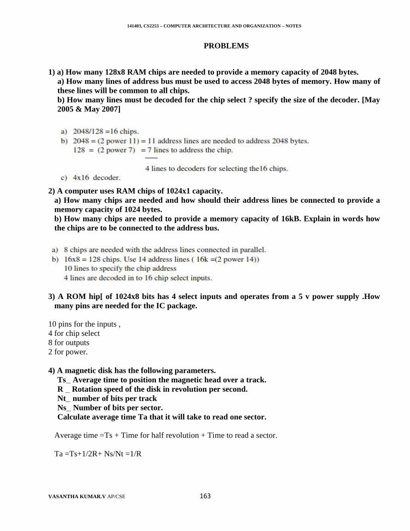
141403, CS2253 – COMPUTER ARCHITECTURE AND ORGANIZATION – NOTES
VASANTHA KUMAR.V AP/CSE 163
PROBLEMS
1) a) How many 128x8 RAM chips are needed to provide a memory capacity of 2048 bytes.a) How many lines of address bus must be used to access 2048 bytes of memory. How many ofthese lines will be common to all chips.b) How many lines must be decoded for the chip select ? specify the size of the decoder. [May2005 & May 2007]
2) A computer uses RAM chips of 1024x1 capacity.a) How many chips are needed and how should their address lines be connected to provide amemory capacity of 1024 bytes.b) How many chips are needed to provide a memory capacity of 16kB. Explain in words howthe chips are to be connected to the address bus.
3) A ROM hip[ of 1024x8 bits has 4 select inputs and operates from a 5 v power supply .Howmany pins are needed for the IC package.
10 pins for the inputs ,4 for chip select8 for outputs2 for power.
4) A magnetic disk has the following parameters.Ts_ Average time to position the magnetic head over a track.R _ Rotation speed of the disk in revolution per second.Nt_ number of bits per trackNs_ Number of bits per sector.Calculate average time Ta that it will take to read one sector.
Average time =Ts + Time for half revolution + Time to read a sector.
Ta =Ts+1/2R+ Ns/Nt =1/R
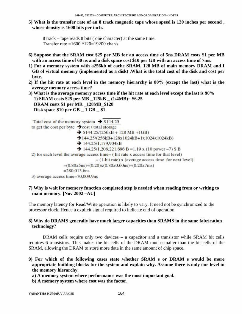
141403, CS2253 – COMPUTER ARCHITECTURE AND ORGANIZATION – NOTES
VASANTHA KUMAR.V AP/CSE 164
5) What is the transfer rate of an 8 track magnetic tape whose speed is 120 inches per second ,whose density is 1600 bits per inch.
8 track – tape reads 8 bits ( one character) at the same time.Transfer rate =1600 *120=19200 char/s
6) Suppose that the SRAM cost $25 per MB for an access time of 5ns DRAM costs $1 per MBwith an access time of 60 ns and a disk space cost $10 per GB with an access time of 7ms.
1) For a memory system with a256kb of cache SRAM, 128 MB of main memory DRAM and IGB of virtual memory (implemented as a disk) .What is the total cost of the disk and cost perbyte.
2) If the hit rate at each level in the memory hierarchy is 80% (except the last) what is theaverage memory access time?
3) What is the average memory access time if the hit rate at each level except the last is 90%1) SRAM costs $25 per MB _125kB _ (1/4MB)= $6.25DRAM costs $1 per MR _128MB_$128Disk space $10 per GB _ 1 GB _ $1
7) Why is wait for memory function completed step is needed when reading from or writing tomain memory. [Nov 2002 –AU]
The memory latency for Read/Write operation is likely to vary. It need not be synchronized to theprocessor clock. Hence a explicit signal required to indicate end of operation.
8) Why do DRAMS generally have much larger capacities than SRAMS in the same fabricationtechnology?
DRAM cells require only two devices – a capacitor and a transistor while SRAM bit cellsrequires 6 transistors. This makes the bit cells of the DRAM much smaller than the bit cells of theSRAM, allowing the DRAM to store more data in the same amount of chip space.
9) For which of the following cases state whether SRAM s or DRAM s would be moreappropriate building blocks for the system and explain why. Assume there is only one level inthe memory hierarchy.a) A memory system where performance was the most important goal.b) A memory system where cost was the factor.
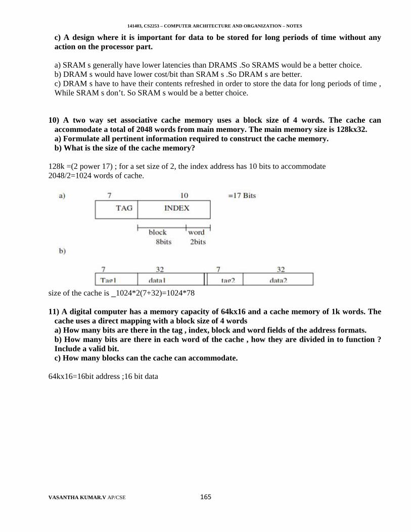
141403, CS2253 – COMPUTER ARCHITECTURE AND ORGANIZATION – NOTES
VASANTHA KUMAR.V AP/CSE 165
c) A design where it is important for data to be stored for long periods of time without anyaction on the processor part.
a) SRAM s generally have lower latencies than DRAMS .So SRAMS would be a better choice.b) DRAM s would have lower cost/bit than SRAM s .So DRAM s are better.c) DRAM s have to have their contents refreshed in order to store the data for long periods of time ,While SRAM s don’t. So SRAM s would be a better choice.
10) A two way set associative cache memory uses a block size of 4 words. The cache canaccommodate a total of 2048 words from main memory. The main memory size is 128kx32.a) Formulate all pertinent information required to construct the cache memory.b) What is the size of the cache memory?
128k =(2 power 17) ; for a set size of 2, the index address has 10 bits to accommodate2048/2=1024 words of cache.
size of the cache is _1024*2(7+32)=1024*78
11) A digital computer has a memory capacity of 64kx16 and a cache memory of 1k words. Thecache uses a direct mapping with a block size of 4 wordsa) How many bits are there in the tag , index, block and word fields of the address formats.b) How many bits are there in each word of the cache , how they are divided in to function ?Include a valid bit.c) How many blocks can the cache can accommodate.
64kx16=16bit address ;16 bit data
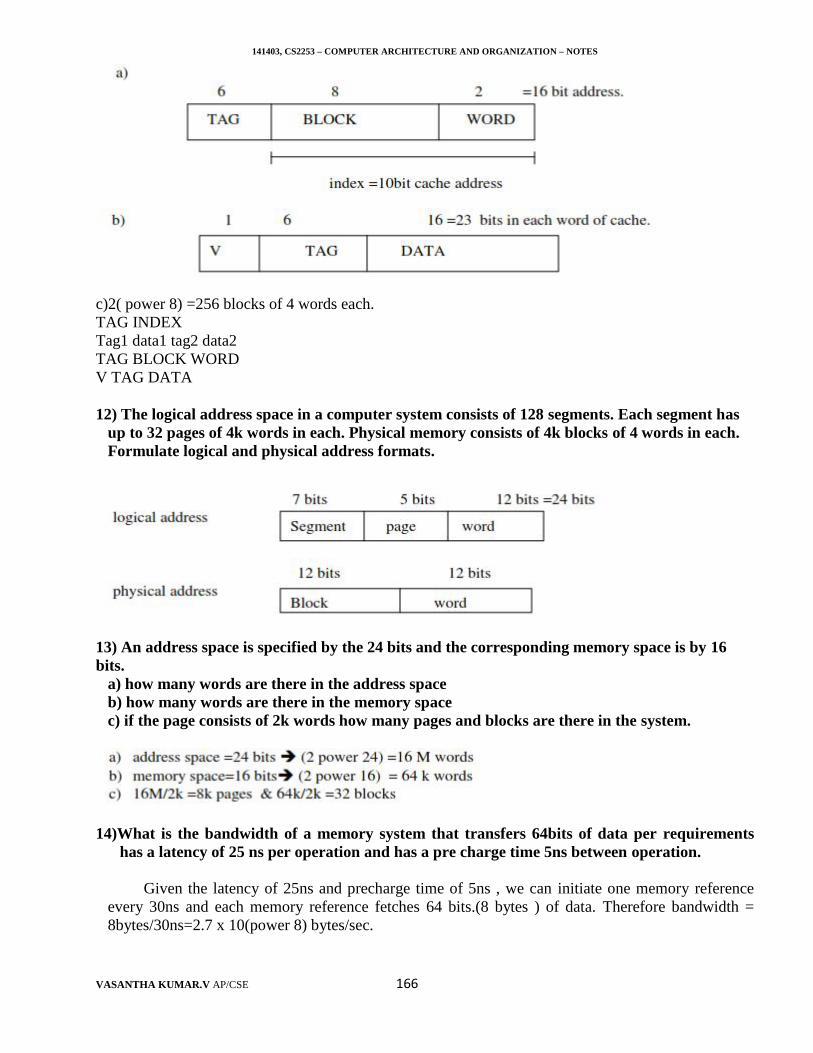
141403, CS2253 – COMPUTER ARCHITECTURE AND ORGANIZATION – NOTES
VASANTHA KUMAR.V AP/CSE 166
c)2( power 8) =256 blocks of 4 words each.TAG INDEXTag1 data1 tag2 data2TAG BLOCK WORDV TAG DATA
12) The logical address space in a computer system consists of 128 segments. Each segment hasup to 32 pages of 4k words in each. Physical memory consists of 4k blocks of 4 words in each.Formulate logical and physical address formats.
13) An address space is specified by the 24 bits and the corresponding memory space is by 16bits.
a) how many words are there in the address spaceb) how many words are there in the memory spacec) if the page consists of 2k words how many pages and blocks are there in the system.
14)What is the bandwidth of a memory system that transfers 64bits of data per requirementshas a latency of 25 ns per operation and has a pre charge time 5ns between operation.
Given the latency of 25ns and precharge time of 5ns , we can initiate one memory referenceevery 30ns and each memory reference fetches 64 bits.(8 bytes ) of data. Therefore bandwidth =8bytes/30ns=2.7 x 10(power 8) bytes/sec.
141403, CS2253 – COMPUTER ARCHITECTURE AND ORGANIZATION – NOTES
VASANTHA KUMAR.V AP/CSE 167
UNIT I
1. What are the functional units of a computer?The functional units of a computer are: input, memory, arithmetic and logic, output,
control units.2. Define program?
A list of instruction that performs a task is called a program.
3. What is a data?
Data are numbers and encoded characters that are used as operands by the instructions.4. What is the function for the memory unit? Give the two classes of the memory unit?
The function for the memory unit is to store program and data. The two classes ofstorage are primary storage and secondary storage.5. What is called primary storage?
Primary storage is the fast memory that operates at electronic speeds. Programs muststore the memory while they are being executed.6. Define memory access time?
The time required to access one word is called the memory access time.7. Define random access memory (RAM)?
Memory in which any location can be reached in a short and fixed amount of time afterspecifying its address is called random-access memory.
8. Define registers?
When operands are brought in to the processor, they are stored in high-speed storageelements called registers.9. What are the operations of a computer?
i. The computer accepts information in the form of programs and data through an
input unit and stores in the memory.
ii. Information stored in the memory is fetched, under program control, into anarithmetic and logic unit, where it is processed.
iii. Processed information leaves the computer through an output unitiv. The control unit directs all activities inside the machine.
10. What is a bus?
A group of lines that serves as a connecting path for several devices is called a bus.
11. Define system software?
It is a collection of programs that are executed as needed to perform functions such asi. Receiving and interpreting user controls.
ii. Entering and editing application programs.iii. Managing the storage and retrival of filesiv. Compiling the I/O units.
12. What is a compiler?A compiler that translates the high-level language program in to a suitable machine language
program.
141403, CS2253 – COMPUTER ARCHITECTURE AND ORGANIZATION – NOTES
VASANTHA KUMAR.V AP/CSE 168
13. Define operating system?It is a large program or a collection of routines that is used to control the sharing of and
interaction among various computer units as they execute application programs.
14. What is a clock?Processor signals are controlled by a timing signal is called a clock.
15. Give the performance equation?T=N x S / RWhere S= machine instruction
R= clock cyclesN=machine language instructions
T=Processor time.16. Give the system Performance Evaluation Corporation (SPEC) rating?
SPEC rating= Running time on the reference computer
Running time on the computer under test
17. What are the two basic memory operations?The two memory operations are: Load and store.
18. Give the general instruction for the three-address type format?Operation Source1, Source2, Destination
19. Define straight-line sequencing?The processor control circuits use the information in the PC to fetch and execute instructions,one at a time, in the order of increasing addresses is called straight-line sequencing.
20. What are the two-phase procedures in executing an n instruction?First phase: Instruction fetchesSecond phase: Instruction execute
21. Define stack pointer?A processor register is used to keep track of the address of the element of the stack that is at thetop at any given time. This register is called the Stack pointer.
22. Tell the difference between how the stack and queue are implemented?
Stack: One end of the stack is fixed while the other end rises and falls as data pushedand popped. A single pointer is needed to point to the top of the stack at any given time.
Queue: Both end of a queue move to higher addresses as the data are added at the backand removed from the front. So two pointers are needed to keep track of the two ends of thequeue
23. Define subroutine?
In a given program, it is often necessary to perform a particular subtask many times on
different values. Such a subtask is called a subroutine.
24. Define machine instruction?
When a program is being executed in a processor, an instruction must be encoded in a
compact binary pattern. Such encoded instructions are called machine instruction.
25. Define assembly language instructions?
The instructions that use symbolic names and acronyms are called assembly language
instructions.
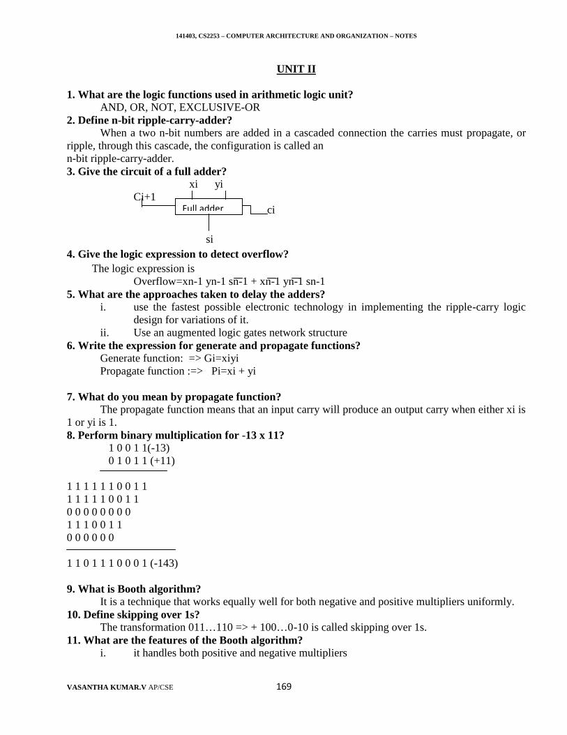
141403, CS2253 – COMPUTER ARCHITECTURE AND ORGANIZATION – NOTES
VASANTHA KUMAR.V AP/CSE 169
UNIT II
1. What are the logic functions used in arithmetic logic unit?AND, OR, NOT, EXCLUSIVE-OR
2. Define n-bit ripple-carry-adder?When a two n-bit numbers are added in a cascaded connection the carries must propagate, or
ripple, through this cascade, the configuration is called ann-bit ripple-carry-adder.3. Give the circuit of a full adder?
xi yiCi+1
ci
si4. Give the logic expression to detect overflow?
The logic expression isOverflow=xn-1 yn-1 sn-1 + xn-1 yn-1 sn-1
5. What are the approaches taken to delay the adders?i. use the fastest possible electronic technology in implementing the ripple-carry logic
design for variations of it.ii. Use an augmented logic gates network structure
6. Write the expression for generate and propagate functions?Generate function: => Gi=xiyiPropagate function :=> Pi=xi + yi
7. What do you mean by propagate function?The propagate function means that an input carry will produce an output carry when either xi is
1 or yi is 1.8. Perform binary multiplication for -13 x 11?
1 0 0 1 1(-13)0 1 0 1 1 (+11)
1 1 1 1 1 1 0 0 1 11 1 1 1 1 0 0 1 10 0 0 0 0 0 0 01 1 1 0 0 1 10 0 0 0 0 0
1 1 0 1 1 1 0 0 0 1 (-143)
9. What is Booth algorithm?It is a technique that works equally well for both negative and positive multipliers uniformly.
10. Define skipping over 1s?The transformation 011…110 => + 100…0-10 is called skipping over 1s.
11. What are the features of the Booth algorithm?i. it handles both positive and negative multipliers
Full adder
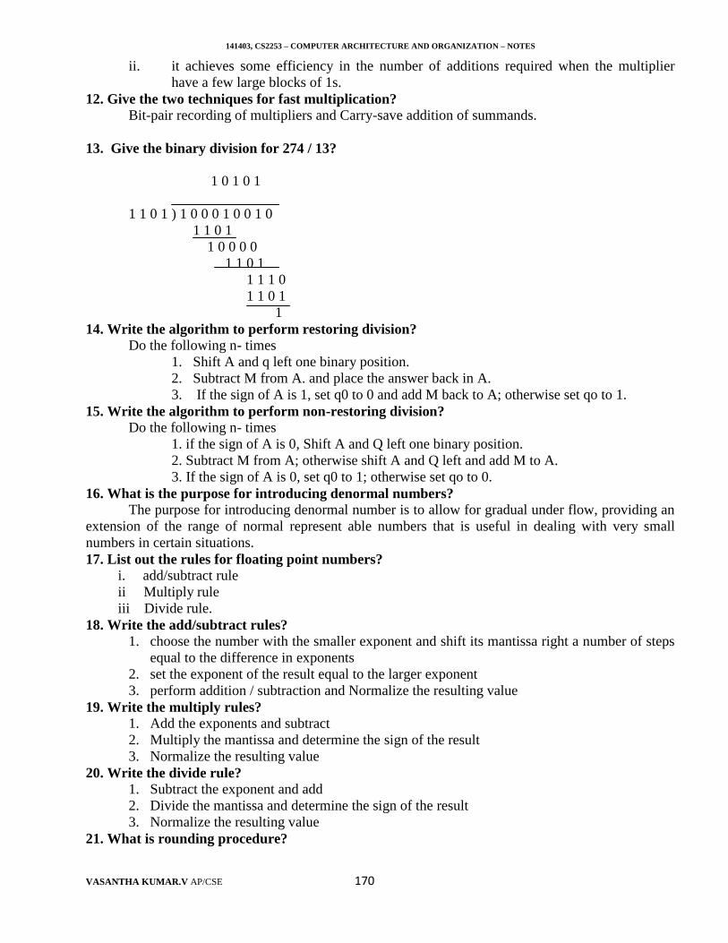
141403, CS2253 – COMPUTER ARCHITECTURE AND ORGANIZATION – NOTES
VASANTHA KUMAR.V AP/CSE 170
ii. it achieves some efficiency in the number of additions required when the multiplierhave a few large blocks of 1s.
12. Give the two techniques for fast multiplication?Bit-pair recording of multipliers and Carry-save addition of summands.
13. Give the binary division for 274 / 13?
1 0 1 0 1
1 1 0 1 ) 1 0 0 0 1 0 0 1 01 1 0 1
1 0 0 0 01 1 0 1
1 1 1 01 1 0 1
114. Write the algorithm to perform restoring division?
Do the following n- times1. Shift A and q left one binary position.2. Subtract M from A. and place the answer back in A.3. If the sign of A is 1, set q0 to 0 and add M back to A; otherwise set qo to 1.
15. Write the algorithm to perform non-restoring division?Do the following n- times
1. if the sign of A is 0, Shift A and Q left one binary position.2. Subtract M from A; otherwise shift A and Q left and add M to A.3. If the sign of A is 0, set q0 to 1; otherwise set qo to 0.
16. What is the purpose for introducing denormal numbers?The purpose for introducing denormal number is to allow for gradual under flow, providing an
extension of the range of normal represent able numbers that is useful in dealing with very smallnumbers in certain situations.17. List out the rules for floating point numbers?
i. add/subtract ruleii Multiply ruleiii Divide rule.
18. Write the add/subtract rules?1. choose the number with the smaller exponent and shift its mantissa right a number of steps
equal to the difference in exponents2. set the exponent of the result equal to the larger exponent3. perform addition / subtraction and Normalize the resulting value
19. Write the multiply rules?1. Add the exponents and subtract2. Multiply the mantissa and determine the sign of the result3. Normalize the resulting value
20. Write the divide rule?1. Subtract the exponent and add2. Divide the mantissa and determine the sign of the result3. Normalize the resulting value
21. What is rounding procedure?
141403, CS2253 – COMPUTER ARCHITECTURE AND ORGANIZATION – NOTES
VASANTHA KUMAR.V AP/CSE 171
Rounding achieves the closest approximation to the number being truncated and is an unbiasedtechnique.22. What Von Neumann rounding?
If the bits to be removed are all 0’s, they are simply dropped, with no changes to the retainedbits.23. What is sticky bit?
If a 1 is shifted out through the position , the bit becomes 1 and retains the value is called asticky bit.24. What is the use of carry-save addition?
Used to speeds up the addition process.25. What is the use of bit-pair recording?
It halves the maximum number of summands.
UNIT III
1. What are the steps taken to perform to execute the instructions?
The following are the steps taken to perform to execute the instructions:1. Fetch the contents of the memory locations pointed to by the PC. The contents of this locations are
interpreted as an instruction to be execute
2. Assuming that the memory is byte addressable, increment the contents of the PC by 4.
3. Carry out the actions specified by the instructions in the IR.
2. Define Data Path?The decoder generates the control signals to select the registers involved and direct the transfer
of the data. The registers, the ALU, the interconnecting bus are collectively referred to as the data
path.
3. Define Multiphase clocking?
When edge-triggered flip-flop are not used, two or more clock signals may be needed to
guarantee proper transfer of data. This is known as multiphase clocking.
4. What is register file?
All general purpose registers are combined into a single block called the register file.
5. What are the actions performed to execute the instructions?
The following are the actions performed to execute the instructions
1. Fetch the instructions
2. Fetch the first operand
3. Perform the addition
4. Load the result into R1
141403, CS2253 – COMPUTER ARCHITECTURE AND ORGANIZATION – NOTES
VASANTHA KUMAR.V AP/CSE 172
6. Define MFC.
MEMORY-FUNCTION-COMPLETED is a control signal which is used to accommodate the
variability in response time the processor waits until it receives an indication that the requested Read
operation has been completed.
7. What do you mean by ISP?
The processing unit which executes machine instructions and coordinates the activities of
other units. The units is often called as Instructions Set Processor (ISP) or simply the processor.
8. Define processor clock?
All operations and data transfer within the processor take place with on time periods defined
by the processor clock.
9. How we can transfer the contents of one register to another?
1. Enable the output of register R1 by setting R1out to 1.This places the contents of R1 on the
processor bus
2. Enable the output of register R4 by setting R4 into 1.This loads data from the processor bus
into register R4.
10. What do you mean by bit-oring technique?
The most efficient way to bypass microinstructions 170 and then use as OR gate to change the
Least significant bit of this address to 1 if the direct addressing mode is involved. This is known as
Bit Oring technique.
11. How the control signals can be determined?
The required control signals csn be determined using the following information:
i. Contents of the control step counter
ii. Contents of the instruction register
iii. Controls of the condition code flags
iv. External input signals, such as MFC and interrupt requests.
12. Define microinstructions?
A sequence of control word’s corresponding to the control sequence of a machine instruction
constitutes the microroutine for that instruction, and the individual control words in this microroutine
are referred to as microinstructions.
13. Define vertical organization?
Highly encoded schemes that use compact codes to specify only a small number of control
functions in each microinstruction are called vertical organization.
14. Define horizontal organization?
141403, CS2253 – COMPUTER ARCHITECTURE AND ORGANIZATION – NOTES
VASANTHA KUMAR.V AP/CSE 173
The minimally encoded scheme, in which many resources can be controlled with a single
microinstruction, is called a horizontal organization.
15. Give the steps involved in executing the statement Move R2, (R1)?
It requires the following sequence:
i. R1out, MARin
ii. R2out, MDRin, Write
iii. MDRoutE, WMFC
16. What are the factors that influence the speed of execution of a program?
i. One way to improve the performance is to use faster circuit technology
ii. Another possibility is to arrange the hardware so that more than one operation can be
performed at the same time.
17. Define hazard?
The condition that causes the pipeline to stall is called a hazard.
18. Define structural hazard?
The situation when two instructions require the use of a given hardware resource at the same
time is called structural hazard
19. Define Side effect?
When a location other than one explicitly named in an instruction as a destination operand is
affected, the instruction is said to be side effect.
20. What is Speculative execution?
Speculative execution means that instructions are executed before the processor is certain that
they are in the correct execution sequence.
21. What are the two key aspects of machine instructions?
Addressing modes and condition code flags
22. What is a control hazard?
The pipeline may also be stalled because of a delay in the availability of an instruction .This
may be a result of a cache miss, requiring the instruction to be fetched from the main memory. Such
hazards are called control hazards.
23. Define delayed branching?
The technique that can minimize the penalty incurred as a result of conditional branch
instructions are called delayed branching.
24. What are the features of an addressing mode?
141403, CS2253 – COMPUTER ARCHITECTURE AND ORGANIZATION – NOTES
VASANTHA KUMAR.V AP/CSE 174
i. Access to an operand does not require more than one access to the memory
ii. Only load and store instructions access memory operands.
iii. The addressing modes used do not have side effects.
25. What the four states that involved in a 4-state algorithm?
ST: Strongly likely to be taken
LT: Likely to be taken
LNT: Likely not to be taken
SNT: Strongly likely not to be taken
UNIT –IV
1. Define memory access time?
The time that elapses between the initiation of an operation and completion of that
operation is called memory access time.
2. Define memory cycle time?
The minimum time delay required between the initiation of two successive memory
operations.
3. What is random access memory?
Any location can be accessed for a read or write operation in some fixed amount of time
that is independent of the locations address.
4. What is a cache memory?
This is a small, fast memory that is inserted between the larger , slower main memory
and the processor. It holds the currently active segment of the program and their data.
5. Define virtual or logical address?
The memory control circuitry translates the address specified by the program in to an
address that can be used to access the physical memory. In such cases the address generated by the
processor is referred to as virtual or logical address.
6. What is memory management unit?
The virtual address space is mapped on to the physical memory where the data is stored.
The mapping function is implemented by a special memory control circuit called memory
management unit.
7. What is a word line?
All cells of a row are connected to a common line, is referred to as word line
8. Define static memories?
Memories that consists of circuits capable of retaining their state as long as power is
applied is known as static memories.
9. Why static RAMs are volatile memories?
141403, CS2253 – COMPUTER ARCHITECTURE AND ORGANIZATION – NOTES
VASANTHA KUMAR.V AP/CSE 175
When power is restored, the latch will settle in to the stable state, but will not
necessarily be the same state the cell was in before the interruption. Hence SRAMs are said to be
volatile memories.
10. Define asynchronous DRAMs?
A specialized memory controller unit provides the necessary control signals, row
address strobe (RAS) and Column address strobe (CAS) that govern the timing. The processor must
take in to account the delay in the response of the memory. Such memories are referred to as
asynchronous DRAMs.
11. Define memory latency?
The amount of time it takes to transfer a word of data to or from the memory. This is
known as memory latency.
12. What is a motherboard?
If a large memory is built by placing DRAM chips directly on the main system printed-circuit
board that contains the processor is referred to as motherboard.
13. What is double-data-rate SDRAMs?
The memory devices transfer data on both edges of the clock; their bandwidth is essentially
doubled for long burst transfers. Such devices are called
double-data-rate SDRAMs.
14. Give the three types of packets?
o Request
o Acknowledge
o Data
15. What are the types of ROM?
PROM
EPROM
EEPROM
16. What is the advantage and disadvantage of EPROM?
The main advantage is that their contents can be erased and reprogrammed. Erasure requires
dissipating the charges trapped in the transistors of memory cells.
The important disadvantage is that a chip must be physically removed from the circuit for
reprogramming and that the ultraviolet light erases its entire contents.
17. Define the term block?
The term block, refer to contiguous address locations of some size.
18. What are the types of mapping functions?
Direct mapping
Associative mapping
141403, CS2253 – COMPUTER ARCHITECTURE AND ORGANIZATION – NOTES
VASANTHA KUMAR.V AP/CSE 176
Set-associative mapping
19. Define hit and hit rate?
A successful access of data is called a hit.The number of hits stated as a fraction of all
attempted accesses is called hit-rate.
20. Define miss penalty?
The extra time needed to bring the desired information into the cache is called the miss penalty.
21. What is page table?
Information about the main memory location is kept in a table .That table is referred to as page
table.
22. Define page frame?
An area in the main memory that can hold one page is called a page frame.
23. What are the major functions of a controller on the disk drive side?
o Seek
o Read
o Write
o Error checking
24. Define floppy disk?
The smaller, simpler, and cheaper disks units that consist of a flexible, removable, plastic
diskette coated with magnetic material known as floppy disk.
25. Define seek time and rotational delay?
Seek time is the time required to move the read/write head to the proper track. Rotational delay
is the amount of time that elapses after the head is positioned over the correct track until the starting
position of the addressed sector passes under the read/write head.
UNIT-V
1. What is memory-mapped I/O?
When I/O devices and the main memory share the same address space, the arrangement is
known as memory-mapped I/O.
2. What is an interrupt?
Interrupt is a hardware signal that can arrange the I/O device to alert the processor when it
becomes ready.
3. Define interrupt service routine?
The routine executed in response to an interrupt request is called interrupt-service routine.
4. Define interrupt latency?
The delay between the time an interrupt request is received and the start of execution of the
interrupt service routine. This delay is called interrupt latency.
141403, CS2253 – COMPUTER ARCHITECTURE AND ORGANIZATION – NOTES
VASANTHA KUMAR.V AP/CSE 177
5. What are the situations in which the interrupts are enabled?
i. The device raises an interrupt request
ii. The processor interrupts the program currently being executed
iii. The action requested by the interrupt is performed by the interrupt service routine
iv. Interrupts are enabled and execution of the interrupted program is resumed
6. What is edge triggered?
The processor has a special interrupt request line for which the interrupt handling circuit
responds only to the leading edge of the signal. Such line is said to be edge triggered.
7. What is an interrupt vector?
The location pointed to by the interrupting device is used to store the starting address of the interrupt
service routine. The processor reads this address, and this is called as interrupt vector.
8. Define privilege exception?
An attempt to execute a privileged instruction while in the user mode leads to a special type of
interrupt. This interrupt is called privilege exception.
9. What are privileged instructions?
To protect the operating system of a computer from being corrupted by user programs, certain
instructions can be executed only while the processor is in the supervisor mode. These are called
privileged instructions.
10. Define multitasking?
Multitasking is a mode of operation in which a processor executes several user programs at the
same time.
11. What is a process?
The OS as an entity regards a program, together with any information that describes its current
state of execution. This is called a process.
12. What is a program state?
The information saved, which includes register contents, the program counter, and the
processor status word. This is called p program state.
13. Give some operating system routines?
OSINIT
OSSERVICES
SHEDULER
IOINIT
IODATA
KBDINIT
14. What is the purpose for OSINIT?
It set the interrupt vectors. That is it set,
141403, CS2253 – COMPUTER ARCHITECTURE AND ORGANIZATION – NOTES
VASANTHA KUMAR.V AP/CSE 178
Time slice clockSCHEDULER
Software interruptOSSERVICES
15. Give the priority for handling the exceptions?
The priority structure is:
Reset
Data abort
FIQ
IRQ
Prefetch abort
Undefined instruction
16. What is data abort and Prefetch abort?
Data abort arises from an error in reading or writing data, and Prefetch abort arises from an
error when perfecting instructions from the memory.
17. Define direct memory access?
A special control; unit may be provided to allow transfer of a block of data directly between an
external device and the main memory, without continuous intervention by the processor. This
approach is called direct memory access (DMA).
18. What is known as burst mode?
The DMA controller may be given the exclusive access to the main memory to transfer a block
of data without interruption. This is known as block or burst mode.
19. What is a bus master?
The device that is allowed to initiate data transfers on the bus at any given time is called a bus
master.
20. What is distributed arbitration?
Distributed arbitration means that all devices waiting to use the bus have equal responsibility
in carrying out the arbitration process, without using a central arbiter.
21. What are called transaction and phases?
A complete transfer operation on the bus, involving an address and a burst of data, is called a
transaction. Individual word transfers within a transaction are called phases.
22. What is an initiator?
The device that initiates data transfers by issuing read or write commands on the bus is called
an initiator.
23. Define full handshake?
A change of state in one signal is followed by a change in the other signal is known as full
handshake.
24. What is a parallel port?

141403, CS2253 – COMPUTER ARCHITECTURE AND ORGANIZATION – NOTES
VASANTHA KUMAR.V AP/CSE 179
A parallel port transfers data in the form of a number of bits, simultaneously to or from the
device.
25. What is a serial port?
A serial port is used to connect the processor to I/O devices that require the transmission of one
bit at a time.