Embed Size (px)
DESCRIPTION
Behrooz Parhami Computer Architecture instructor manual
Citation preview

Jan. 2011 Computer Architecture, Background and Motivation Slide 1
Part IBackground and Motivation

Jan. 2011 Computer Architecture, Background and Motivation Slide 2
About This PresentationThis presentation is intended to support the use of the textbookComputer Architecture: From Microprocessors to Supercomputers, Oxford University Press, 2005, ISBN 0-19-515455-X. It is updated regularly by the author as part of his teaching of the upper-division course ECE 154, Introduction to Computer Architecture, at the University of California, Santa Barbara. Instructors can use these slides freely in classroom teaching and for other educational purposes. Any other use is strictly prohibited. © Behrooz Parhami
Edition Released Revised Revised Revised RevisedFirst June 2003 July 2004 June 2005 Mar. 2006 Jan. 2007
Jan. 2008 Jan. 2009 Jan. 2011
Second
Jan. 2011 Computer Architecture, Background and Motivation Slide 3
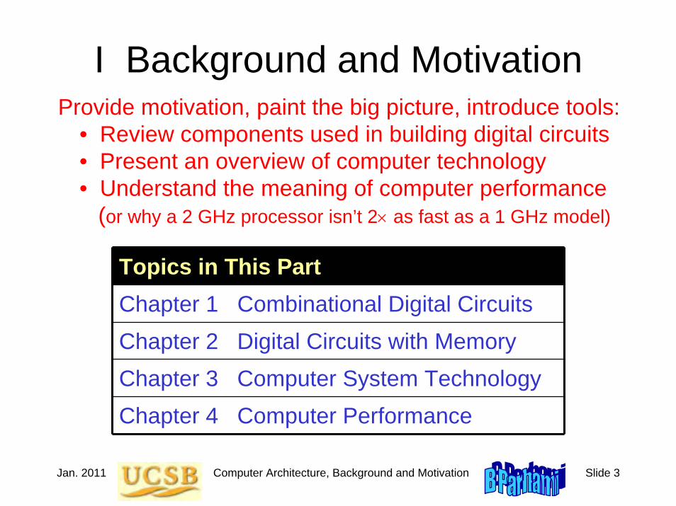
I Background and Motivation
Topics in This PartChapter 1 Combinational Digital CircuitsChapter 2 Digital Circuits with MemoryChapter 3 Computer System TechnologyChapter 4 Computer Performance
Provide motivation, paint the big picture, introduce tools:• Review components used in building digital circuits• Present an overview of computer technology• Understand the meaning of computer performance
(or why a 2 GHz processor isn’t 2× as fast as a 1 GHz model)
Jan. 2011 Computer Architecture, Background and Motivation Slide 4
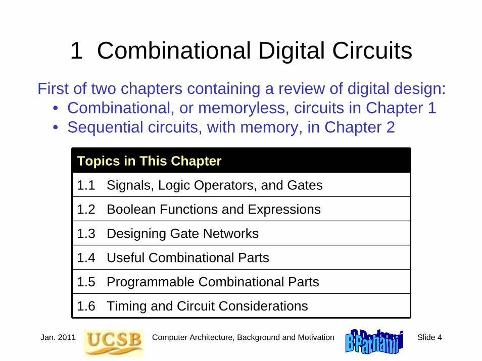
1 Combinational Digital CircuitsFirst of two chapters containing a review of digital design:
• Combinational, or memoryless, circuits in Chapter 1• Sequential circuits, with memory, in Chapter 2
Topics in This Chapter
1.1 Signals, Logic Operators, and Gates
1.2 Boolean Functions and Expressions
1.3 Designing Gate Networks
1.4 Useful Combinational Parts
1.5 Programmable Combinational Parts
1.6 Timing and Circuit Considerations

Jan. 2011 Computer Architecture, Background and Motivation Slide 5
1.1 Signals, Logic Operators, and Gates
Figure 1.1 Some basic elements of digital logic circuits, with operator signs used in this book highlighted.
x ≡ y /
AND Name XOR OR NOT
Graphical symbol
x ∧ y
Operator sign and alternate(s)
x ⊕ y x ∨ y xy x + y
x ′ ¬x or x
_
x × y or xy Arithmetic expression
x + y − 2xyx + y − xy 1 − x
Output is 1 iff: Input is 0 Both inputs
are 1s At least one
input is 1 Inputs are not equal

Jan. 2011 Computer Architecture, Background and Motivation Slide 6
The Arithmetic Substitution Method
z ′ = 1 – z NOT converted to arithmetic formxy AND same as multiplication
(when doing the algebra, set zk = z)x ∨ y = x + y − xy OR converted to arithmetic formx ⊕ y = x + y − 2xy XOR converted to arithmetic form
Example: Prove the identity xyz ∨ x ′ ∨ y ′ ∨ z ′ ≡? 1
LHS = [xyz ∨ x ′] ∨ [y ′ ∨ z ′]= [xyz + 1 – x – (1 – x)xyz] ∨ [1 – y + 1 – z – (1 – y)(1 – z)]= [xyz + 1 – x] ∨ [1 – yz]= (xyz + 1 – x) + (1 – yz) – (xyz + 1 – x)(1 – yz) = 1 + xy2z2 – xyz= 1 = RHS This is addition,
not logical OR

Jan. 2011 Computer Architecture, Background and Motivation Slide 7
Variations in Gate Symbols
Figure 1.2 Gates with more than two inputs and/or with inverted signals at input or output.
OR NOR NAND AND XNOR

Jan. 2011 Computer Architecture, Background and Motivation Slide 8
Gates as Control Elements
Figure 1.3 An AND gate and a tristate buffer act as controlled switches or valves. An inverting buffer is logically the same as a NOT gate.
Enable/Pass signal e
Data in x
Data out x or 0
Data in x
Enable/Pass signal e
Data out x or “high impedance”
(a) AND gate for controlled transfer (b) Tristate buffer
(c) Model for AND switch.
x
e
No data or x
0 1 x
e
ex
0 1
0
(d) Model for tristate buffer.
Jan. 2011 Computer Architecture, Background and Motivation Slide 9
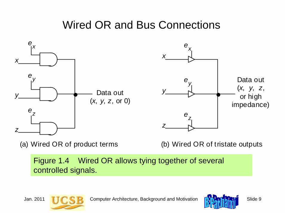
Wired OR and Bus Connections
Figure 1.4 Wired OR allows tying together of several controlled signals.
e
e
e Data out (x, y, z, or high
impedance)
(b) Wired OR of t ristate outputs
e
e
e
Data out (x, y, z, or 0)
(a) Wired OR of product terms
z
x
y
z
x
y
z
x
y
z
x
y

Jan. 2011 Computer Architecture, Background and Motivation Slide 10
Control/Data Signals and Signal Bundles
Figure 1.5 Arrays of logic gates represented by a single gate symbol.
/ 8
/
8 / 8
Compl
/ 32
/ k
/ 32
Enable
/ k
/ k
/ k
(b) 32 AND gates (c) k XOR gates (a) 8 NOR gates

Jan. 2011 Computer Architecture, Background and Motivation Slide 11
1.2 Boolean Functions and Expressions
Ways of specifying a logic function
• Truth table: 2n row, “don’t-care” in input or output
• Logic expression: w ′ (x ∨ y ∨ z), product-of-sums,sum-of-products, equivalent expressions
• Word statement: Alarm will sound if the dooris opened while the security system is engaged, or when the smoke detector is triggered
• Logic circuit diagram: Synthesis vs analysis

Jan. 2011 Computer Architecture, Background and Motivation Slide 12
Table 1.2 Laws (basic identities) of Boolean algebra.
Name of law OR version AND versionIdentity x ∨ 0 = x x 1 = x
One/Zero x ∨ 1 = 1 x 0 = 0
Idempotent x ∨ x = x x x = x
Inverse x ∨ x ′ = 1 x x ′ = 0
Commutative x ∨ y = y ∨ x x y = y x
Associative (x ∨ y) ∨ z = x ∨ (y ∨ z) (x y) z = x (y z)
Distributive x ∨ (y z) = (x ∨ y) (x ∨ z) x (y ∨ z) = (x y) ∨ (x z)
DeMorgan’s (x ∨ y)′ = x ′ y ′ (x y)′ = x ′ ∨ y ′
Manipulating Logic Expressions

Jan. 2011 Computer Architecture, Background and Motivation Slide 13
Proving the Equivalence of Logic ExpressionsExample 1.1
• Truth-table method: Exhaustive verification
• Arithmetic substitutionx ∨ y = x + y − xyx ⊕ y = x + y − 2xy
• Case analysis: two cases, x = 0 or x = 1
• Logic expression manipulation
Example: x ⊕ y ≡? x ′y∨xy ′x + y – 2xy ≡? (1–x)y + x(1–y) – (1–x)yx(1–y)
Jan. 2011 Computer Architecture, Background and Motivation Slide 14
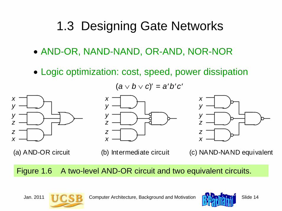
1.3 Designing Gate Networks
• AND-OR, NAND-NAND, OR-AND, NOR-NOR
• Logic optimization: cost, speed, power dissipation
(a) AND-OR circuit
z
x y
x
y z
(b) Intermediate circuit (c) NAND-NAND equivalent
z
x y
x
y z z
x y
x
y z
Figure 1.6 A two-level AND-OR circuit and two equivalent circuits.
(a ∨ b ∨ c)′ = a ′b ′c ′

Jan. 2011 Computer Architecture, Background and Motivation Slide 15
Seven-Segment Display of Decimal Digits
Figure 1.7 Seven-segment display of decimal digits. The three open segments may be optionally used. The digit 1 can be displayed in two ways, with the more common right-side version shown.
Optional segment

Jan. 2011 Computer Architecture, Background and Motivation Slide 16
BCD-to-Seven-Segment Decoder
Example 1.2
Figure 1.8 The logic circuit that generates the enable signal for the lowermost segment (number 3) in a seven-segment display unit.
x 3 x 2 x 1 x 0
Signals to enable or turn on the segments
4-bit input in [0, 9] e0
e 5
e 6
e 4
e 2
e 1
e 3
1
2 4
5
0
3
6
Jan. 2011 Computer Architecture, Background and Motivation Slide 17
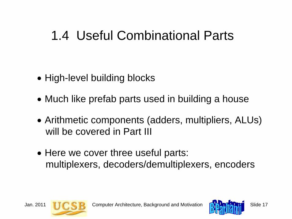
1.4 Useful Combinational Parts
• High-level building blocks
• Much like prefab parts used in building a house
• Arithmetic components (adders, multipliers, ALUs) will be covered in Part III
• Here we cover three useful parts:multiplexers, decoders/demultiplexers, encoders

Jan. 2011 Computer Architecture, Background and Motivation Slide 18
Multiplexers
Figure 1.9 Multiplexer (mux), or selector, allows one of several inputs to be selected and routed to output depending on the binary value of a set of selection or address signals provided to it.
x
x
y
z
1
0
x
x
z
y
x x
y
z
1
0
y
/ 32
/ 32
/ 32 1
0
1
0
3
2
z
y 1 0
1
0
1
0
y 1
y 0
y 0
(a) 2-to-1 mux (b) Switch view (c) Mux symbol
(d) Mux array (e) 4-to-1 mux with enable (e) 4-to-1 mux design
0
1
y
1 1
1
0
0 0
x x x x
1 0
2 3
x
x
x
x
0
1
2
3
z
e (Enable)
1 0
x2

Computer Architecture, Background and Motivation Slide 19
Decoders/Demultiplexers
Figure 1.10 A decoder allows the selection of one of 2a options using an a-bit address as input. A demultiplexer (demux) is a decoder that only selects an output if its enable signal is asserted.
y 1 y 0
x 0
x 3
x 2
x 1
1
0
3
2
y 1 y 0
x 0
x 3
x 2
x 1 e
1
0
3
2
y 1 y 0
x 0
x 3
x 2
x 1
(a) 2-to-4 decoder (b) Decoder symbol (c) Demultiplexer, or decoder with “enable”
(Enable) 1
1 0
1
1 0
11 1
Jan. 2011

Jan. 2011 Computer Architecture, Background and Motivation Slide 20
Encoders
Figure 1.11 A 2a-to-a encoder outputs an a-bit binary number equal to the index of the single 1 among its 2a inputs.
(a) 4-to-2 encoder (b) Encoder symbol
x 0
x 3
x 2
x 1
y 1 y 0
1
0
3
2
x 0
x 3
x 2
x 1
y 1 y 0
1 0
1
0
0
0

Jan. 2011 Computer Architecture, Background and Motivation Slide 21
1.5 Programmable Combinational Parts
• Programmable ROM (PROM)
• Programmable array logic (PAL)
• Programmable logic array (PLA)
A programmable combinational part can do the job of many gates or gate networks
Programmed by cutting existing connections (fuses) or establishing new connections (antifuses)

Jan. 2011 Computer Architecture, Background and Motivation Slide 22
PROMs
Figure 1.12 Programmable connections and their use in a PROM.
. . .
.
.
.
Inputs
Outputs
(a) Programmable OR gates
w
x
y
z
(b) Logic equivalent of part a
w
x
y
z
(c) Programmable read-only memory (PROM)
Dec
oder

Jan. 2011 Computer Architecture, Background and Motivation Slide 23
PALs and PLAs
Figure 1.13 Programmable combinational logic: general structure and two classes known as PAL and PLA devices. Not shown is PROM withfixed AND array (a decoder) and programmable OR array.
AND array (AND plane)
OR array (OR
plane)
. . .
. . .
.
.
.
Inputs
Outputs
(a) General programmable combinational logic
(b) PAL: programmable AND array, fixed OR array
8-input ANDs
(c) PLA: programmable AND and OR arrays
6-input ANDs
4-input ORs

Jan. 2011 Computer Architecture, Background and Motivation Slide 24
1.6 Timing and Circuit Considerations
• Gate delay δ: a fraction of, to a few, nanoseconds
• Wire delay, previously negligible, is now important(electronic signals travel about 15 cm per ns)
• Circuit simulation to verify function and timing
Changes in gate/circuit output, triggered by changes in its inputs, are not instantaneous

Jan. 2011 Computer Architecture, Background and Motivation Slide 25
Glitching
Figure 1.14 Timing diagram for a circuit that exhibits glitching.
x = 0
y
z
a = x ∨ y
f = a ∨ z 2δ 2δ
Using the PAL in Fig. 1.13b to implement f = x ∨ y ∨ z
AND-OR(PAL)
AND-OR(PAL)
xyz
af
Jan. 2011 Computer Architecture, Background and Motivation Slide 26
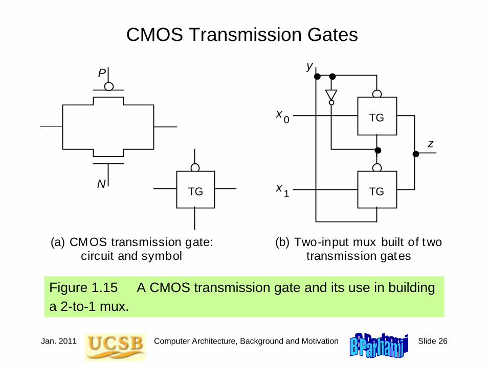
CMOS Transmission Gates
Figure 1.15 A CMOS transmission gate and its use in buildinga 2-to-1 mux.
z
x
x
0
1
(a) CMOS transmission gate: circuit and symbol
(b) Two-input mux built of two transmission gates
TG
TG TG
y P
N

Jan. 2011 Computer Architecture, Background and Motivation Slide 27
2 Digital Circuits with MemorySecond of two chapters containing a review of digital design:
• Combinational (memoryless) circuits in Chapter 1• Sequential circuits (with memory) in Chapter 2
Topics in This Chapter
2.1 Latches, Flip-Flops, and Registers2.2 Finite-State Machines2.3 Designing Sequential Circuits2.4 Useful Sequential Parts2.5 Programmable Sequential Parts2.6 Clocks and Timing of Events

Jan. 2011 Computer Architecture, Background and Motivation Slide 28
2.1 Latches, Flip-Flops, and Registers
Figure 2.1 Latches, flip-flops, and registers.
R Q
Q′ S
D Q
Q′ C
Q
Q′
D
C
(a) SR latch (b) D latch
Q
C
Q
D
Q
C
Q
D
(e) k -bit register(d) D flip-flop symbol (c) Master-slave D flip-flop
Q
C
Q
D FF
/
/
k
k
Q
C
Q
D FF
R
S

Jan. 2011 Computer Architecture, Background and Motivation Slide 29
Latches vs Flip-Flops
Figure 2.2 Operations of D latch and negative-edge-triggered D flip-flop.
D
C
D latch: Q
D FF: Q
Setup time
Setup time
Hold time
Hold time
D
C
Q
Q
D
C
Q
QFF

Jan. 2011 Computer Architecture, Background and Motivation Slide 30
Reading and Modifying FFs in the Same Cycle
Figure 2.3 Register-to-register operation with edge-triggered flip-flops.
/
/
k
k
Q
C
Q
D FF
/
/
k
k
Q
C
Q
D FF
Computation module (combinational logic)
Clock Propagation delay Combinational delay

Jan. 2011 Computer Architecture, Background and Motivation Slide 31
2.2 Finite-State MachinesExample 2.1
Figure 2.4 State table and state diagram for a vending machine coin reception unit.
Dime Dime Quarter
Dime
Quarter
Dime Quarter
Dime Quarter
Reset Reset
Reset
Reset
Reset
Start Quarter
S 00 S 10 S 20 S 25 S 30 S 35
S 10 S 25 S 00 S 00 S 00 S 00 S 00 S 00
S 20 S 35
S 35 S 35
S 35 S 35
S 35 S 30
S 35 S 35
------- Input ------- D
ime
Qua
rter
Res
et Current
state
S 00 S 35
is the initial state is the final state
Next state
Dime Quarter
S 00
S 10 S 20
S 25
S 30 S 35

Jan. 2011 Computer Architecture, Background and Motivation Slide 32
Sequential Machine Implementation
Figure 2.5 Hardware realization of Moore and Mealy sequential machines.
Next-state logic
State register / n
/ m
/ l
Inputs Outputs
Next-state excitation signals
Present state
Output logic
Only for Mealy machine
Jan. 2011 Computer Architecture, Background and Motivation Slide 33
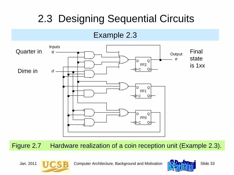
2.3 Designing Sequential CircuitsExample 2.3
Figure 2.7 Hardware realization of a coin reception unit (Example 2.3).
Output
Q C
Q
D
e
Inputs
Q C
Q
D
Q C
Q
D
FF2
FF1
FF0
q
d
Quarter in
Dime in
Final state is 1xx

Jan. 2011 Computer Architecture, Background and Motivation Slide 34
2.4 Useful Sequential Parts
• High-level building blocks
• Much like prefab closets used in building a house
• Other memory components will be covered in Chapter 17 (SRAM details, DRAM, Flash)
• Here we cover three useful parts:shift register, register file (SRAM basics), counter
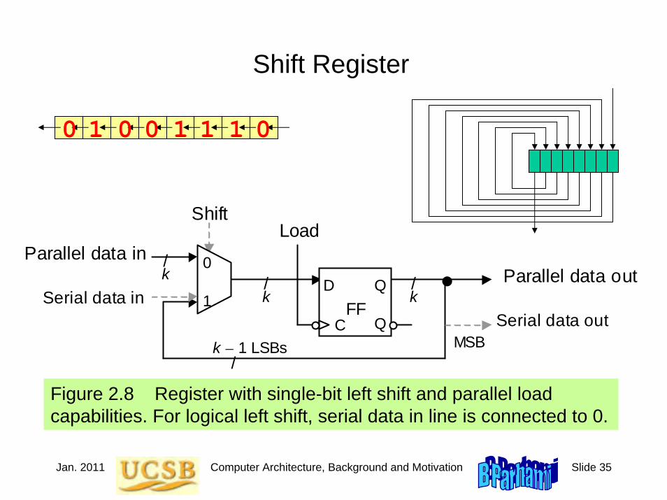
Jan. 2011 Computer Architecture, Background and Motivation Slide 35
Shift Register
Figure 2.8 Register with single-bit left shift and parallel load capabilities. For logical left shift, serial data in line is connected to 0.
Parallel data in / k
/ k
/ k
Shift
Q C
Q
D FF
1
0
Serial data in
/
k – 1 LSBs
Load
Parallel data out
Serial data out MSB
0 1 0 0 1 1 1 0

Jan. 2011 Computer Architecture, Background and Motivation Slide 36
Register File and FIFO
Figure 2.9 Register file with random access and FIFO.
Dec
oder
/ k
/ k
/
h
Write enable
Read address 0
Read address 1
Read data 0
Write data
Read enable
2 k -bit registersh / k
/ k
/ k
/ k
/ k
/ k
/ k
/ h
Write address
Muxes
Read data 1
/
k
/
h
/ h / h
/ k / h
Write enable
Read addr 0
/ k / k
Read addr 1
Write data Write addr
Read data 0
Read enable
Read data 1
(a) Register file with random access
(b) Graphic symbol for register file
Q C
Q
D FF
/ k
Q C
Q
D FF
Q C
Q
D FF
Q C
Q
D FF
/ k
Push
/ k
Input
Output Pop
Full
Empty
(c) FIFO symbol

Jan. 2011 Computer Architecture, Background and Motivation Slide 37
SRAM
Figure 2.10 SRAM memory is simply a large, single-port register file.
Column mux
Row
dec
oder
/ h
Address
Square or almost square memory matrix
Row buffer
Row
Column g bits data out
/ g / h
Write enable
/ g
Data in
Address
Data out
Output enable
Chip select
.
.
.
. . .
. . .
(a) SRAM block diagram (b) SRAM read mechanism
Jan. 2011 Computer Architecture, Background and Motivation Slide 38
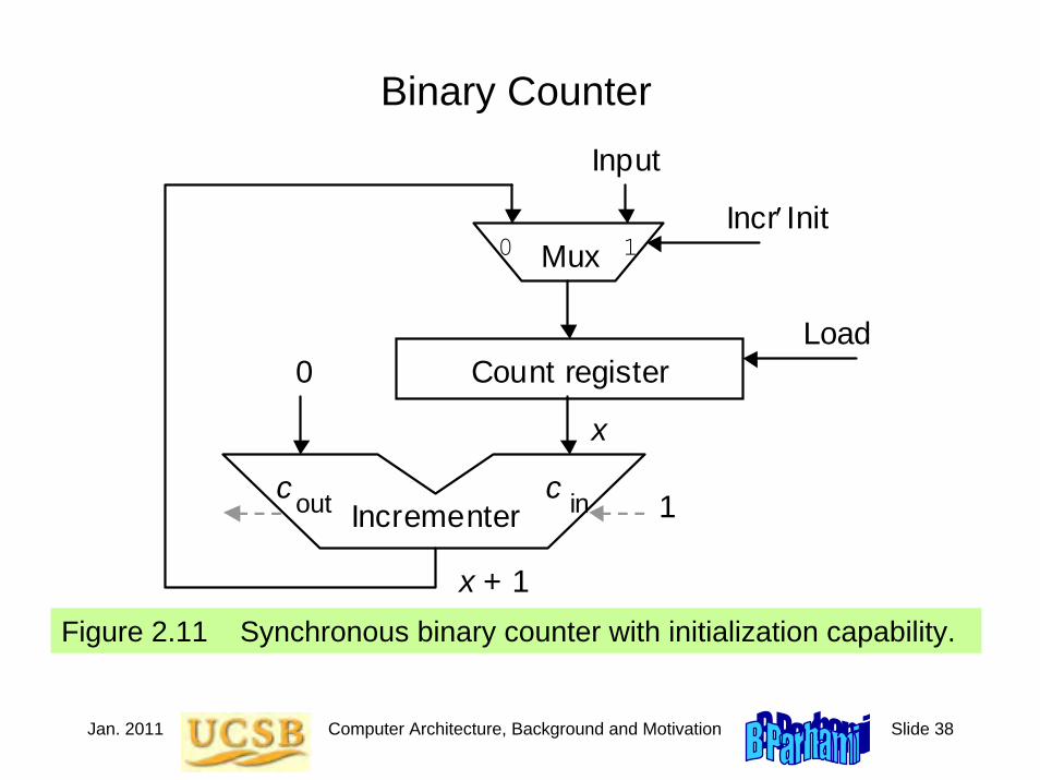
Binary Counter
Figure 2.11 Synchronous binary counter with initialization capability.
Count register
Mux
Incrementer
0
Input
Load
Incr′Init
x + 1
x
0 1
1 c in c out

Jan. 2011 Computer Architecture, Background and Motivation Slide 39
2.5 Programmable Sequential Parts
• Programmable array logic (PAL)
• Field-programmable gate array (FPGA)
• Both types contain macrocells and interconnects
A programmable sequential part contain gates and memory elements
Programmed by cutting existing connections (fuses) or establishing new connections (antifuses)

Jan. 2011 Computer Architecture, Background and Motivation Slide 40
PAL and FPGA
Figure 2.12 Examples of programmable sequential logic.
(a) Portion of PAL with storable output (b) Generic structure of an FPGA
8-input ANDs
D
C Q
Q
FF
Mux
Mux
0 1
0 1
I/O blocks
Configurable logic block
Programmable connections
CLB
CLB
CLB
CLB
Jan. 2011 Computer Architecture, Background and Motivation Slide 41
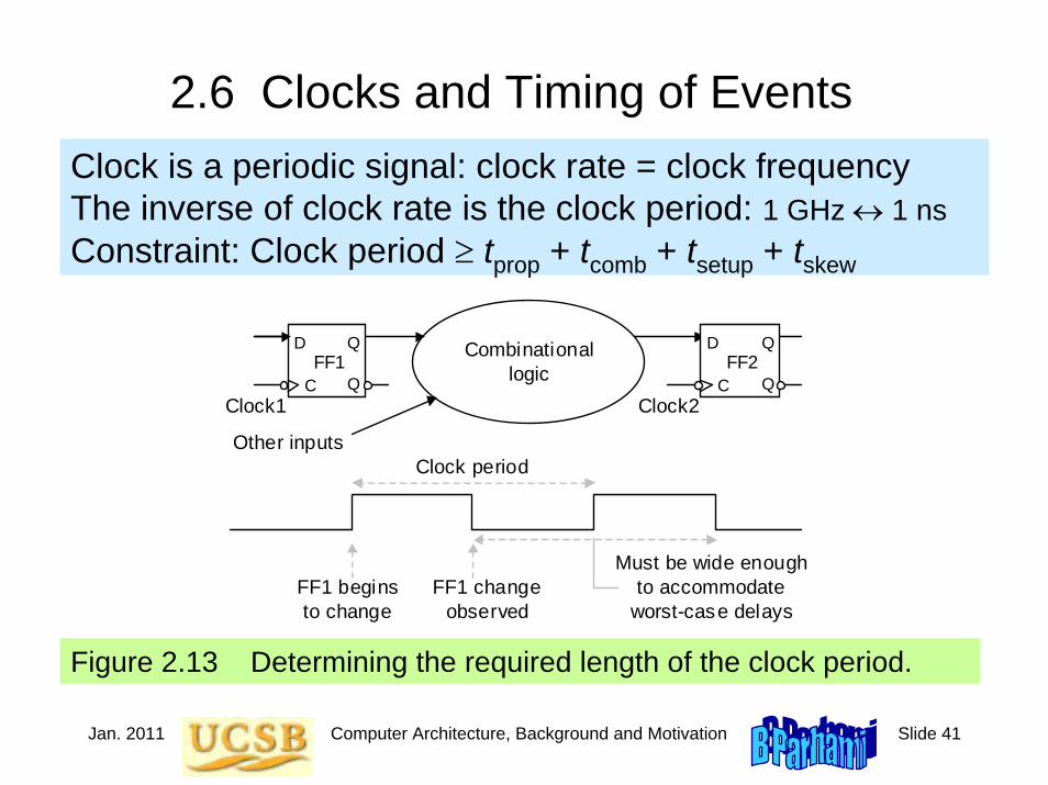
2.6 Clocks and Timing of EventsClock is a periodic signal: clock rate = clock frequencyThe inverse of clock rate is the clock period: 1 GHz ↔ 1 nsConstraint: Clock period ≥ tprop + tcomb + tsetup + tskew
Figure 2.13 Determining the required length of the clock period.
Other inputs
Combinational logic
Clock period
FF1 begins to change
FF1 change observed
Must be wide enough to accommodate
worst-case delays
Clock1 Clock2
Q C
Q
D
FF2
Q C
Q
D
FF1

Jan. 2011 Computer Architecture, Background and Motivation Slide 42
Synchronization
Figure 2.14 Synchronizers are used to prevent timing problemsarising from untimely changes in asynchronous signals.
Asynch input
Asynch input
Synch version
Synch version
Asynch input
Synch version
Clock
(a) Simple synchronizer (b) Two-FF synchronizer
(c) Input and output waveforms
Q
C
Q
D
FF
Q
C
Q
D
FF2
Q
C
Q
D
FF1
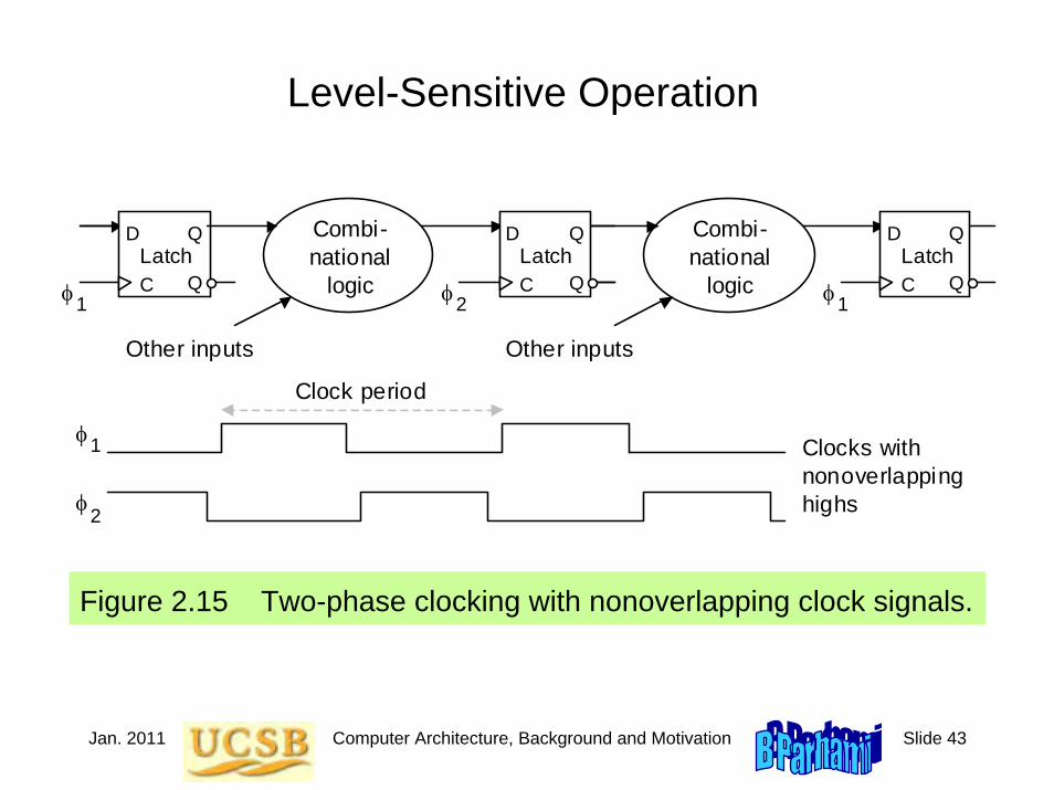
Jan. 2011 Computer Architecture, Background and Motivation Slide 43
Level-Sensitive Operation
Figure 2.15 Two-phase clocking with nonoverlapping clock signals.
Combi- national
logic 1 φ 1
Clock period
φ
Q C
Q
D
Latch
1 φ
Q C
Q
D
Latch
Other inputs
Combi- national
logic 2 φ
2 φ
Clocks with nonoverlapping highs
Other inputs
Q C
Q
Latch
D

Jan. 2011 Computer Architecture, Background and Motivation Slide 44
3 Computer System TechnologyInterplay between architecture, hardware, and software
• Architectural innovations influence technology• Technological advances drive changes in architecture
Topics in This Chapter3.1 From Components to Applications
3.2 Computer Systems and Their Parts
3.3 Generations of Progress
3.4 Processor and Memory Technologies
3.5 Peripherals, I/O, and Communications
3.6 Software Systems and Applications

Jan. 2011 Computer Architecture, Background and Motivation Slide 45
3.1 From Components to Applications
Figure 3.1 Subfields or views in computer system engineering.
High-level view
Com
pute
r de
sign
er
Circ
uit d
esig
ner
App
licat
ion
desi
gner
Sys
tem
des
igne
r
Logi
c de
sign
er
Software
Hardware
Computer organization
Low-level view
App
licat
ion
dom
ains
Ele
ctro
nic
com
pone
nts
Computer architecture
Jan. 2011 Computer Architecture, Background and Motivation Slide 46
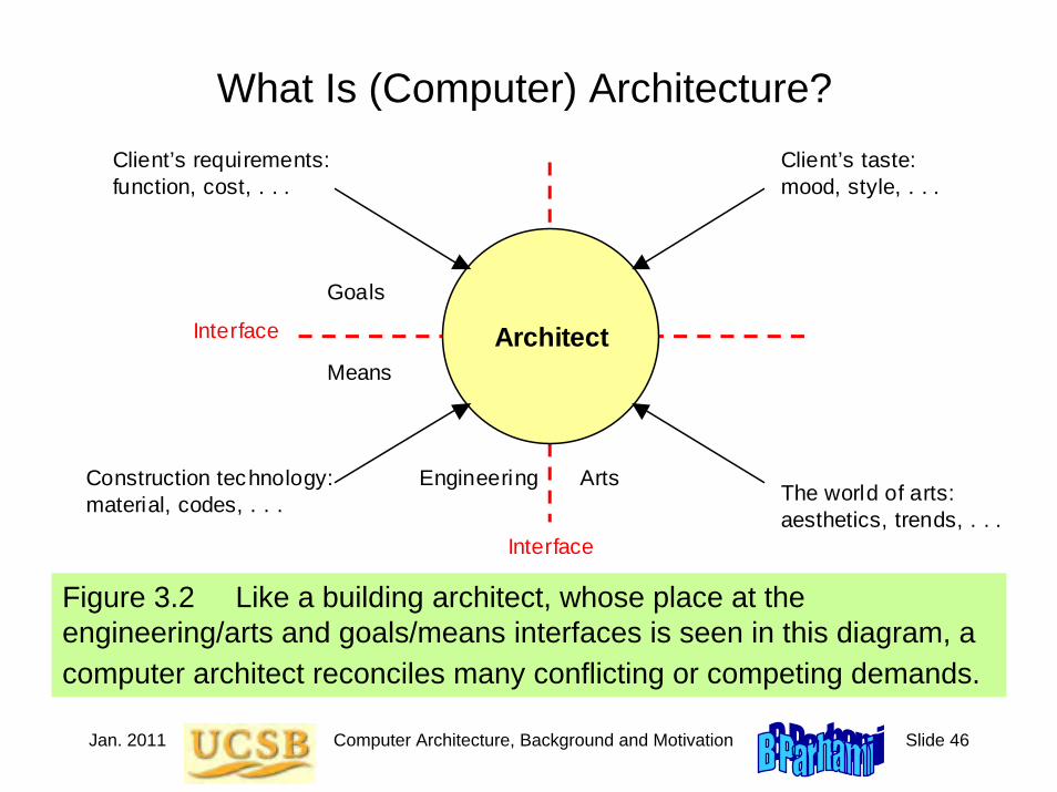
What Is (Computer) Architecture?
Figure 3.2 Like a building architect, whose place at the engineering/arts and goals/means interfaces is seen in this diagram, a computer architect reconciles many conflicting or competing demands.
Architect Interface
Interface
Goals
Means
Arts Engineering
Client’s taste: mood, style, . . .
Client’s requirements: function, cost, . . .
The world of arts: aesthetics, trends, . . .
Construction technology: material, codes, . . .

Jan. 2011 Computer Architecture, Background and Motivation Slide 47
3.2 Computer Systems and Their Parts
Figure 3.3 The space of computer systems, with what we normally mean by the word “computer” highlighted.
Computer
Analog
Fixed-function Stored-program
Electronic Nonelectronic
General-purpose Special-purpose
Number cruncher Data manipulator
Digital

Jan. 2011 Computer Architecture, Background and Motivation Slide 48
Price/Performance Pyramid
Figure 3.4 Classifying computers by computational power and price range.
Embedded Personal
Workstation
Server
Mainframe
Super $Millions$100s Ks
$10s Ks
$1000s
$100s
$10s
Differences in scale, not in substance

Jan. 2011 Computer Architecture, Background and Motivation Slide 49
Automotive Embedded Computers
Figure 3.5 Embedded computers are ubiquitous, yet invisible. They are found in our automobiles, appliances, and many other places.
Engine
Impact sensors
Navigation & entertainment
Central control ler
Brakes Airbags

Jan. 2011 Computer Architecture, Background and Motivation Slide 50
Personal Computers and Workstations
Figure 3.6 Notebooks, a common class of portable computers, are much smaller than desktops but offer substantially the same capabilities. What are the main reasons for the size difference?

Jan. 2011 Computer Architecture, Background and Motivation Slide 51
Digital Computer Subsystems
Figure 3.7 The (three, four, five, or) six main units of a digital computer. Usually, the link unit (a simple bus or a more elaborate network) is not explicitly included in such diagrams.
Memory
Link Input/Output
To/from network
Processor
Control
Datapath
Input
Output
CPU I/O

Jan. 2011 Computer Architecture, Background and Motivation Slide 52
3.3 Generations of ProgressTable 3.2 The 5 generations of digital computers, and their ancestors.
Generation (begun)
Processor technology
Memory innovations
I/O devices introduced
Dominant look & fell
0 (1600s) (Electro-) mechanical
Wheel, card Lever, dial, punched card
Factory equipment
1 (1950s) Vacuum tube Magnetic drum
Paper tape, magnetic tape
Hall-size cabinet
2 (1960s) Transistor Magnetic core
Drum, printer, text terminal
Room-size mainframe
3 (1970s) SSI/MSI RAM/ROM chip
Disk, keyboard, video monitor
Desk-size mini
4 (1980s) LSI/VLSI SRAM/DRAM Network, CD, mouse,sound
Desktop/ laptop micro
5 (1990s) ULSI/GSI/ WSI, SOC
SDRAM, flash
Sensor/actuator, point/click
Invisible, embedded

Jan. 2011 Computer Architecture, Background and Motivation Slide 53
Figure 3.8 The manufacturing process for an IC part.
IC Production and Yield
15-30 cm
30-60 cm
Silicon crystal ingot
Slicer Processing: 20-30 steps
Blank wafer with defects
x x x x x x x
x x x x
0.2 cm
Patterned wafer
(100s of simple or scores of complex processors)
Dicer Die
~1 cm
Good die
~1 cm
Die tester
Microchip or other part
Mounting Part
tester Usable
part to ship
Jan. 2011 Computer Architecture, Background and Motivation Slide 54
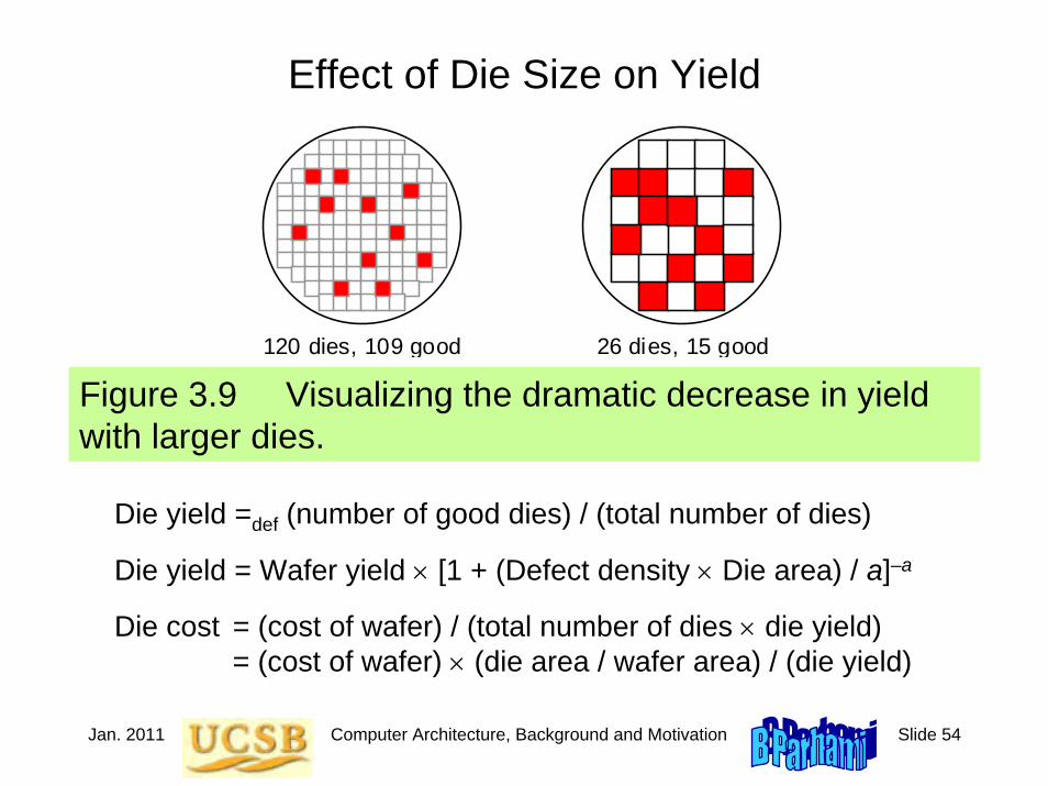
Figure 3.9 Visualizing the dramatic decrease in yield with larger dies.
Effect of Die Size on Yield
120 dies, 109 good 26 dies, 15 good
Die yield =def (number of good dies) / (total number of dies)
Die yield = Wafer yield × [1 + (Defect density × Die area) / a]–a
Die cost = (cost of wafer) / (total number of dies × die yield)= (cost of wafer) × (die area / wafer area) / (die yield)

Jan. 2011 Computer Architecture, Background and Motivation Slide 55
3.4 Processor and Memory Technologies
Figure 3.11 Packaging of processor, memory, and other components.
PC board
Backplane
Memory
CPU
Bus
Connector
(b) 3D packaging of the future (a) 2D or 2.5D packaging now common
Stacked layers glued together
Interlayer connections deposited on the
outside of the stack Die
Jan. 2011 Computer Architecture, Background and Motivation Slide 56
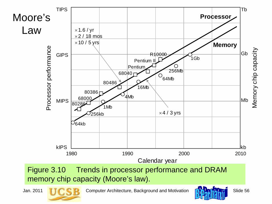
Figure 3.10 Trends in processor performance and DRAM memory chip capacity (Moore’s law).
Moore’s Law
1Mb
1990 1980 2000 2010 kIPS
MIPS
GIPS
TIPS
Pro
cess
or p
erfo
rman
ce
Calendar year
80286 68000
80386
80486
68040 Pentium
Pentium II R10000
×1.6 / yr
×10 / 5 yrs ×2 / 18 mos
64Mb
4Mb
64kb
256kb
256Mb
1Gb
16Mb
×4 / 3 yrs
Processor
Memory
kb
Mb
Gb
Tb
Mem
ory
chip
cap
acity

Jan. 2011 Computer Architecture, Background and Motivation Slide 57
Pitfalls of Computer Technology Forecasting
“DOS addresses only 1 MB of RAM because we cannot imagine any applications needing more.” Microsoft, 1980
“640K ought to be enough for anybody.” Bill Gates, 1981
“Computers in the future may weigh no more than 1.5 tons.” Popular Mechanics
“I think there is a world market for maybe five computers.” Thomas Watson, IBM Chairman, 1943
“There is no reason anyone would want a computer in their home.” Ken Olsen, DEC founder, 1977
“The 32-bit machine would be an overkill for a personal computer.” Sol Libes, ByteLines

Jan. 2011 Computer Architecture, Background and Motivation Slide 58
3.5 Input/Output and Communications
Figure 3.12 Magnetic and optical disk memory units.
(a) Cutaway view of a hard disk drive (b) Some removable storage media
Typically 2-9 cm
Floppy disk
CD-ROM
Magnetic tape
cartridge
. .
. . . . . .
Jan. 2011 Computer Architecture, Background and Motivation Slide 59
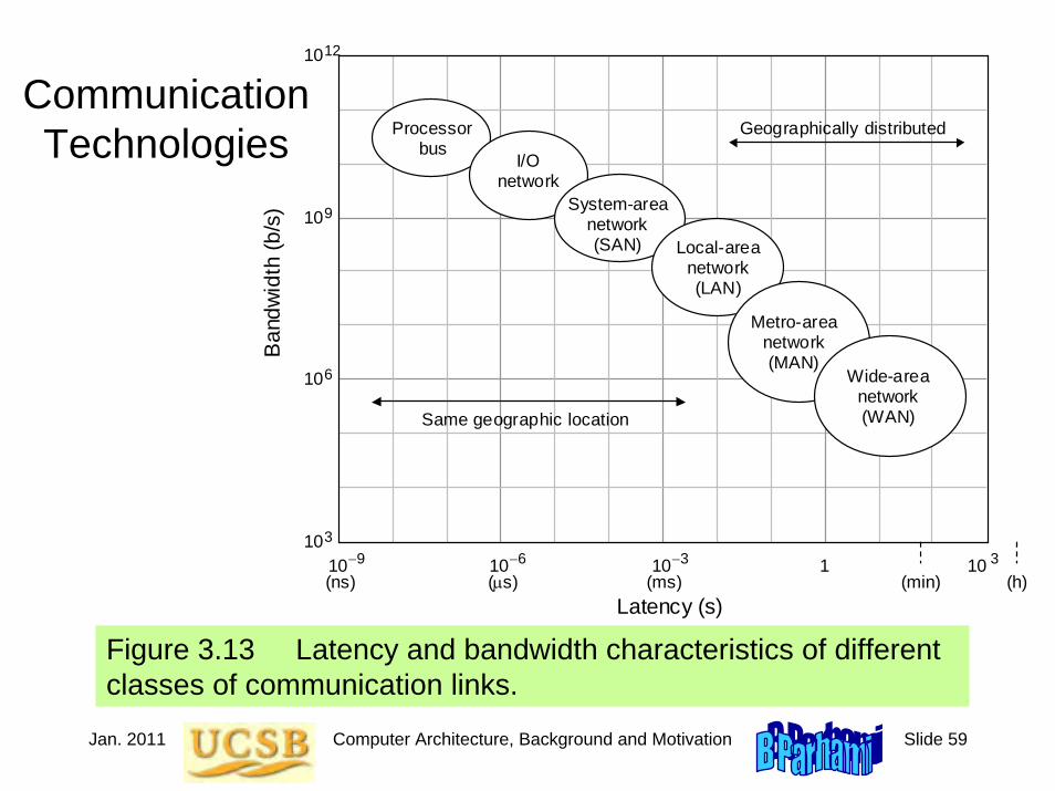
Figure 3.13 Latency and bandwidth characteristics of different classes of communication links.
Communication Technologies
3
6
9
12
−9 −6 −3 3
Ban
dwid
th (b
/s)
Latency (s)
10
10
10
10
10 10 10 1 10
Processor bus
I/O
network
System-area
network (SAN)
Local-area
network (LAN)
Metro-area
network (MAN)
Wide-area
network (WAN)
Geographically distributed
Same geographic location
(ns) (μs) (ms) (min) (h)

Jan. 2011 Computer Architecture, Background and Motivation Slide 60
3.6 Software Systems and Applications
Figure 3.15 Categorization of software, with examples in each class.
Software
Application: word processor,
spreadsheet, circuit simulator,
. . . Operating system Translator:
MIPS assembler, C compiler,
. . .
System
Manager: virtual memory,
security, file system,
. . .
Coordinator: scheduling,
load balancing, diagnostics,
. . .
Enabler: disk driver,
display driver, printing,
. . .

Jan. 2011 Computer Architecture, Background and Motivation Slide 61
Figure 3.14 Models and abstractions in programming.
High- vs Low-Level Programming
Com
pile
r
Ass
embl
er
Inte
rpre
ter
temp=v[i] v[i]=v[i+1] v[i+1]=temp
Swap v[i] and v[i+1]
add $2,$5,$5 add $2,$2,$2 add $2,$4,$2 lw $15,0($2) lw $16,4($2) sw $16,0($2) sw $15,4($2) jr $31
00a51020 00421020 00821020 8c620000 8cf20004 acf20000 ac620004 03e00008
Very high-level language objectives or tasks
High-level language statements
Assembly language instructions, mnemonic
Machine language instructions, binary (hex)
One task = many statements
One statement = several instructions
Mostly one-to-one
More abstract, machine-independent; easier to write, read, debug, or maintain
More conc rete, machine-specific, error-prone; harder to write, read, debug, or maintain
Jan. 2011 Computer Architecture, Background and Motivation Slide 62
4 Computer PerformancePerformance is key in design decisions; also cost and power
• It has been a driving force for innovation• Isn’t quite the same as speed (higher clock rate)
Topics in This Chapter4.1 Cost, Performance, and Cost/Performance
4.2 Defining Computer Performance
4.3 Performance Enhancement and Amdahl’s Law
4.4 Performance Measurement vs Modeling
4.5 Reporting Computer Performance
4.6 The Quest for Higher Performance

Jan. 2011 Computer Architecture, Background and Motivation Slide 63
4.1 Cost, Performance, and Cost/Performance
1980 1960 2000 2020$1
Com
pute
r cos
t
Calendar year
$1 K
$1 M
$1 G
Jan. 2011 Computer Architecture, Background and Motivation Slide 64
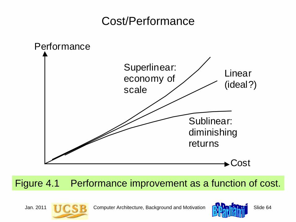
Figure 4.1 Performance improvement as a function of cost.
Cost/Performance
Performance
Cost
Superlinear: economy of scale
Sublinear: diminishing returns
Linear (ideal?)

Jan. 2011 Computer Architecture, Background and Motivation Slide 65
4.2 Defining Computer Performance
Figure 4.2 Pipeline analogy shows that imbalance between processing power and I/O capabilities leads to a performance bottleneck.
Processing Input Output
CPU-bound task
I/O-bound task

Jan. 2011 Computer Architecture, Background and Motivation Slide 66
Six Passenger Aircraft to Be ComparedB 747
DC-8-50
Jan. 2011 Computer Architecture, Background and Motivation Slide 67
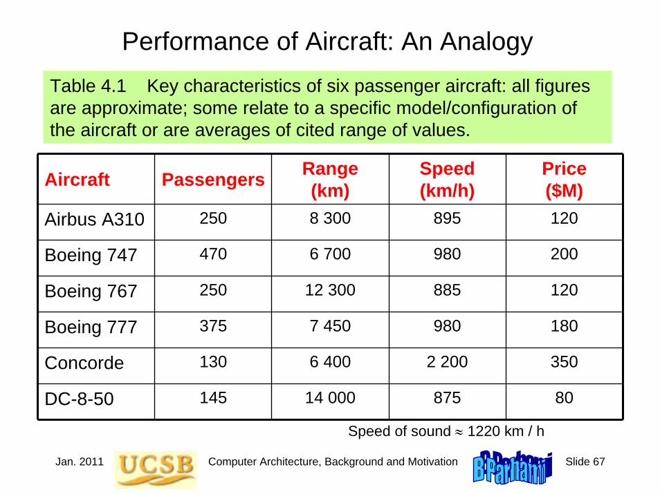
Performance of Aircraft: An AnalogyTable 4.1 Key characteristics of six passenger aircraft: all figures are approximate; some relate to a specific model/configuration of the aircraft or are averages of cited range of values.
Aircraft Passengers Range (km)
Speed (km/h)
Price ($M)
Airbus A310 250 8 300 895 120
Boeing 747 470 6 700 980 200
Boeing 767 250 12 300 885 120
Boeing 777 375 7 450 980 180
Concorde 130 6 400 2 200 350
DC-8-50 145 14 000 875 80
Speed of sound ≈ 1220 km / h
Jan. 2011 Computer Architecture, Background and Motivation Slide 68
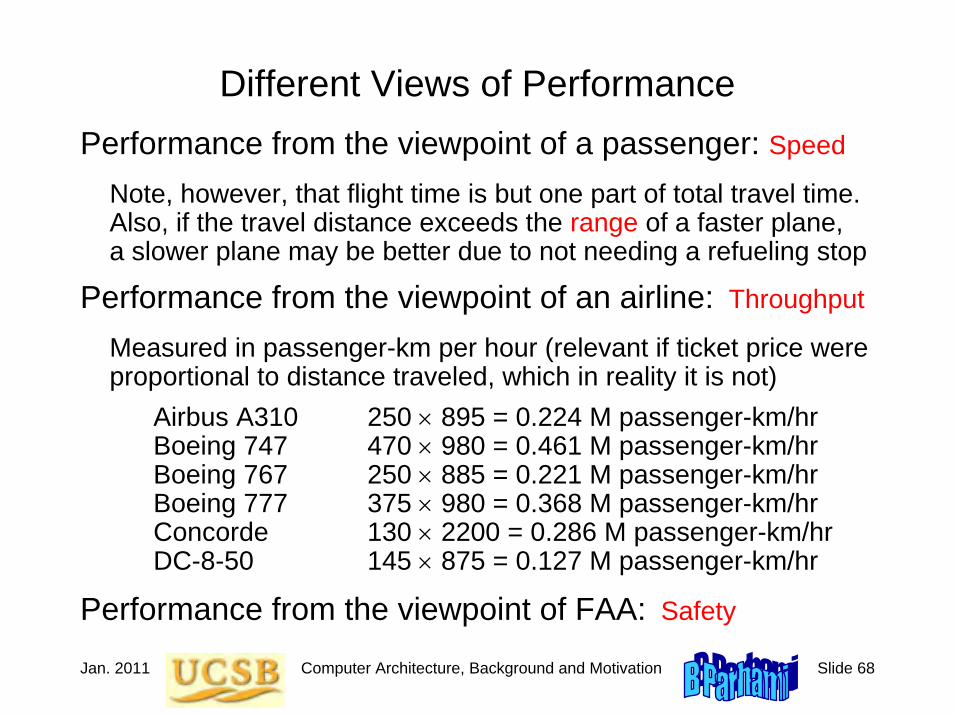
Different Views of PerformancePerformance from the viewpoint of a passenger: Speed
Note, however, that flight time is but one part of total travel time.Also, if the travel distance exceeds the range of a faster plane, a slower plane may be better due to not needing a refueling stop
Performance from the viewpoint of an airline: Throughput
Measured in passenger-km per hour (relevant if ticket price were proportional to distance traveled, which in reality it is not)
Airbus A310 250 × 895 = 0.224 M passenger-km/hrBoeing 747 470 × 980 = 0.461 M passenger-km/hrBoeing 767 250 × 885 = 0.221 M passenger-km/hrBoeing 777 375 × 980 = 0.368 M passenger-km/hrConcorde 130 × 2200 = 0.286 M passenger-km/hrDC-8-50 145 × 875 = 0.127 M passenger-km/hr
Performance from the viewpoint of FAA: Safety

Jan. 2011 Computer Architecture, Background and Motivation Slide 69
Cost Effectiveness: Cost/PerformanceTable 4.1 Key characteristics of six passenger aircraft: all figures are approximate; some relate to a specific model/configuration of the aircraft or are averages of cited range of values.Aircraft Passen-
gersRange (km)
Speed (km/h)
Price ($M)
A310 250 8 300 895 120
B 747 470 6 700 980 200
B 767 250 12 300 885 120
B 777 375 7 450 980 180
Concorde 130 6 400 2 200 350
DC-8-50 145 14 000 875 80
Cost /Performance
536
434
543
489
1224
630
Smallervaluesbetter
Throughput(M P km/hr)
0.224
0.461
0.221
0.368
0.286
0.127
Largervaluesbetter

Jan. 2011 Computer Architecture, Background and Motivation Slide 70
Concepts of Performance and Speedup
Performance = 1 / Execution time is simplified to
Performance = 1 / CPU execution time
(Performance of M1) / (Performance of M2) = Speedup of M1 over M2= (Execution time of M2) / (Execution time M1)
Terminology: M1 is x times as fast as M2 (e.g., 1.5 times as fast)M1 is 100(x – 1)% faster than M2 (e.g., 50% faster)
CPU time = Instructions × (Cycles per instruction) × (Secs per cycle)= Instructions × CPI / (Clock rate)
Instruction count, CPI, and clock rate are not completely independent, so improving one by a given factor may not lead to overall execution time improvement by the same factor.

Jan. 2011 Computer Architecture, Background and Motivation Slide 71
Elaboration on the CPU Time Formula
CPU time = Instructions × (Cycles per instruction) × (Secs per cycle)= Instructions × Average CPI / (Clock rate)
Clock period
Clock rate: 1 GHz = 109 cycles / s (cycle time 10–9 s = 1 ns)200 MHz = 200 × 106 cycles / s (cycle time = 5 ns)
Average CPI: Is calculated based on the dynamic instruction mixand knowledge of how many clock cycles are neededto execute various instructions (or instruction classes)
Instructions: Number of instructions executed, not number of instructions in our program (dynamic count)

Jan. 2011 Computer Architecture, Background and Motivation Slide 72
Dynamic Instruction Count
250 instructionsfor i = 1, 100 do20 instructions
for j = 1, 100 do40 instructions
for k = 1, 100 do10 instructionsendfor
endforendfor
How many instructions are executed in this program fragment?
Each “for” consists of two instructions: increment index, check exit condition
2 + 40 + 1200 instructions100 iterations124,200 instructions in all
2 + 10 instructions100 iterations1200 instructions in all
2 + 20 + 124,200 instructions100 iterations12,422,200 instructions in all
12,422,450 Instructions
for i = 1, nwhile x > 0
Static count = 326
Jan. 2011 Computer Architecture, Background and Motivation Slide 73
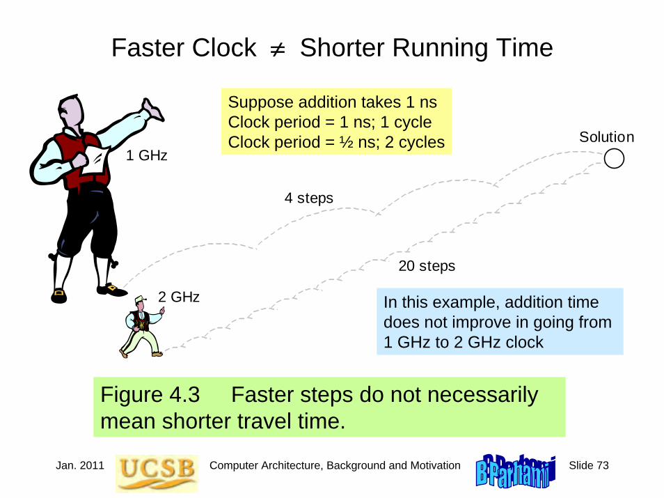
Figure 4.3 Faster steps do not necessarily mean shorter travel time.
Faster Clock ≠ Shorter Running Time
1 GHz
2 GHz
4 steps
Solution
20 steps
Suppose addition takes 1 nsClock period = 1 ns; 1 cycleClock period = ½ ns; 2 cycles
In this example, addition time does not improve in going from 1 GHz to 2 GHz clock

Jan. 2011 Computer Architecture, Background and Motivation Slide 74
0
10
20
30
40
50
0 10 20 30 40 50Enhancement factor (p )
Spe
edup
(s)
f = 0
f = 0.1
f = 0.05
f = 0.02
f = 0.01
4.3 Performance Enhancement: Amdahl’s Law
Figure 4.4 Amdahl’s law: speedup achieved if a fraction f of a task is unaffected and the remaining 1 – f part runs p times as fast.
s =
≤ min(p, 1/f)
1f+ (1 – f)/p
f = fraction unaffected
p = speedup of the rest
Jan. 2011 Computer Architecture, Background and Motivation Slide 75
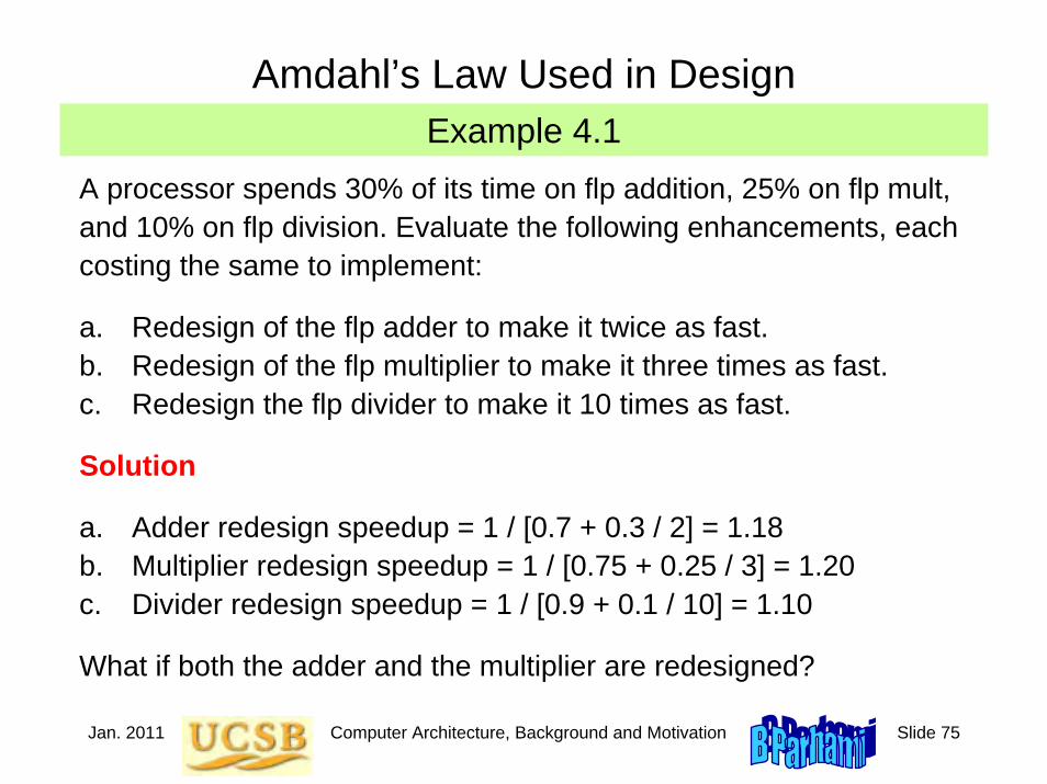
Example 4.1 Amdahl’s Law Used in Design
A processor spends 30% of its time on flp addition, 25% on flp mult, and 10% on flp division. Evaluate the following enhancements, each costing the same to implement:
a. Redesign of the flp adder to make it twice as fast.b. Redesign of the flp multiplier to make it three times as fast.c. Redesign the flp divider to make it 10 times as fast.
Solution
a. Adder redesign speedup = 1 / [0.7 + 0.3 / 2] = 1.18b. Multiplier redesign speedup = 1 / [0.75 + 0.25 / 3] = 1.20c. Divider redesign speedup = 1 / [0.9 + 0.1 / 10] = 1.10
What if both the adder and the multiplier are redesigned?
Jan. 2011 Computer Architecture, Background and Motivation Slide 76
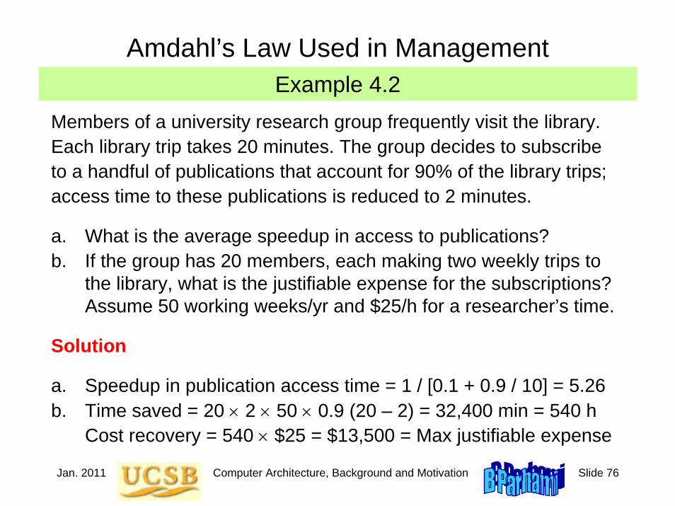
Example 4.2 Amdahl’s Law Used in Management
Members of a university research group frequently visit the library. Each library trip takes 20 minutes. The group decides to subscribe to a handful of publications that account for 90% of the library trips; access time to these publications is reduced to 2 minutes.
a. What is the average speedup in access to publications?b. If the group has 20 members, each making two weekly trips to
the library, what is the justifiable expense for the subscriptions? Assume 50 working weeks/yr and $25/h for a researcher’s time.
Solution
a. Speedup in publication access time = 1 / [0.1 + 0.9 / 10] = 5.26b. Time saved = 20 × 2 × 50 × 0.9 (20 – 2) = 32,400 min = 540 h
Cost recovery = 540 × $25 = $13,500 = Max justifiable expense
Jan. 2011 Computer Architecture, Background and Motivation Slide 77
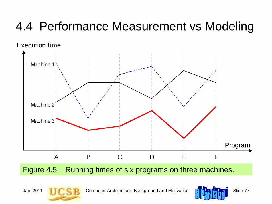
4.4 Performance Measurement vs Modeling
Figure 4.5 Running times of six programs on three machines.
Execution time
Program
A E F B C D
Machine 1
Machine 2
Machine 3
Jan. 2011 Computer Architecture, Background and Motivation Slide 78
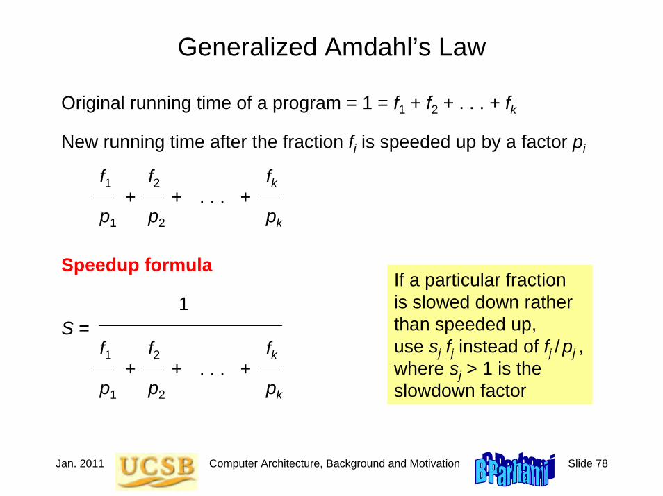
Generalized Amdahl’s Law
Original running time of a program = 1 = f1 + f2 + . . . + fk
New running time after the fraction fi is speeded up by a factor pi
f1 f2 fk+ + . . . +
p1 p2 pk
Speedup formula
1S =
f1 f2 fk+ + . . . +
p1 p2 pk
If a particular fraction is slowed down rather than speeded up, use sj fj instead of fj /pj , where sj > 1 is the slowdown factor
Jan. 2011 Computer Architecture, Background and Motivation Slide 79
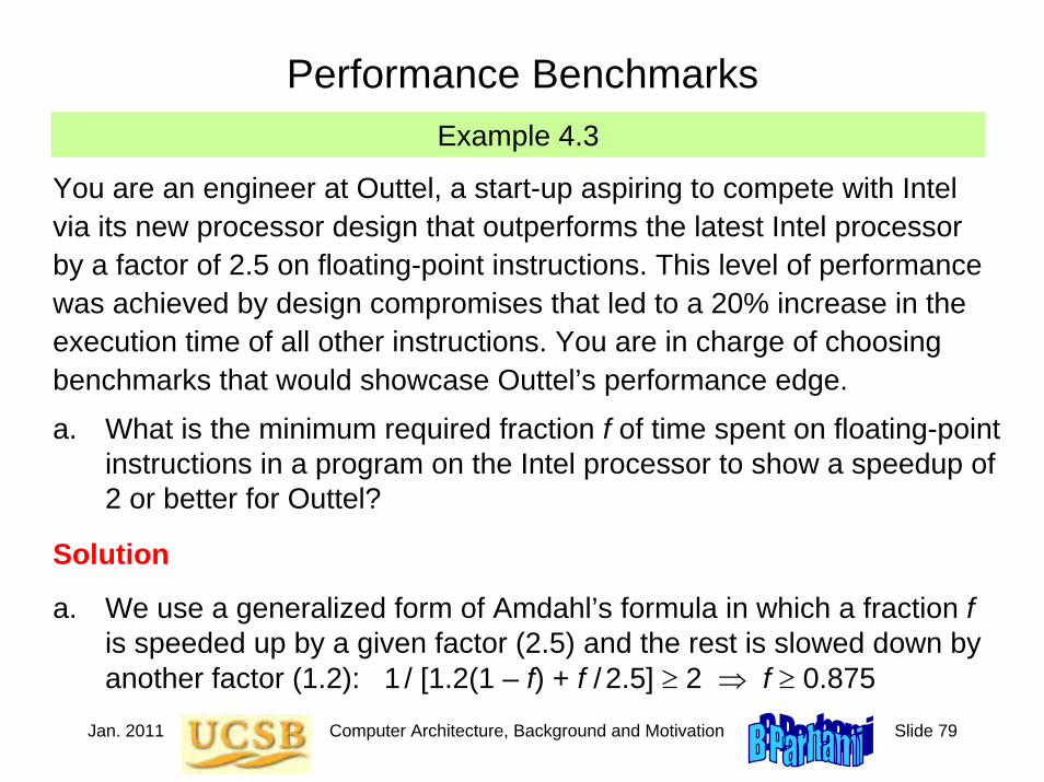
Performance BenchmarksExample 4.3
You are an engineer at Outtel, a start-up aspiring to compete with Intel via its new processor design that outperforms the latest Intel processor by a factor of 2.5 on floating-point instructions. This level of performance was achieved by design compromises that led to a 20% increase in the execution time of all other instructions. You are in charge of choosing benchmarks that would showcase Outtel’s performance edge.
a. What is the minimum required fraction f of time spent on floating-point instructions in a program on the Intel processor to show a speedup of 2 or better for Outtel?
Solution
a. We use a generalized form of Amdahl’s formula in which a fraction fis speeded up by a given factor (2.5) and the rest is slowed down by another factor (1.2): 1 / [1.2(1 – f) + f / 2.5] ≥ 2 ⇒ f ≥ 0.875

Jan. 2011 Computer Architecture, Background and Motivation Slide 80
Performance EstimationAverage CPI = ∑All instruction classes (Class-i fraction) × (Class-i CPI)
Machine cycle time = 1 / Clock rate
CPU execution time = Instructions × (Average CPI) / (Clock rate)
Table 4.3 Usage frequency, in percentage, for various instruction classes in four representative applications.
Application →Instr’n class ↓
Data compression
C language compiler
Reactor simulation
Atomic motion modeling
A: Load/Store 25 37 32 37B: Integer 32 28 17 5C: Shift/Logic 16 13 2 1D: Float 0 0 34 42E: Branch 19 13 9 10F: All others 8 9 6 4

Jan. 2011 Computer Architecture, Background and Motivation Slide 81
CPI and IPS CalculationsExample 4.4 (2 of 5 parts)
Consider two implementations M1 (600 MHz) and M2 (500 MHz) of an instruction set containing three classes of instructions:
Class CPI for M1 CPI for M2 CommentsF 5.0 4.0 Floating-pointI 2.0 3.8 Integer arithmeticN 2.4 2.0 Nonarithmetic
a. What are the peak performances of M1 and M2 in MIPS?b. If 50% of instructions executed are class-N, with the rest divided
equally among F and I, which machine is faster? By what factor?
Solution
a. Peak MIPS for M1 = 600 / 2.0 = 300; for M2 = 500 / 2.0 = 250b. Average CPI for M1 = 5.0 / 4 + 2.0 / 4 + 2.4 / 2 = 2.95;
for M2 = 4.0 /4 + 3.8 / 4 + 2.0 / 2 = 2.95 → M1 is faster; factor 1.2
Jan. 2011 Computer Architecture, Background and Motivation Slide 82
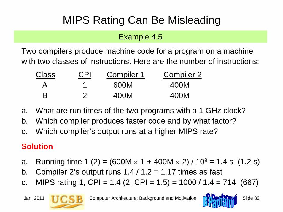
MIPS Rating Can Be MisleadingExample 4.5
Two compilers produce machine code for a program on a machine with two classes of instructions. Here are the number of instructions:
Class CPI Compiler 1 Compiler 2A 1 600M 400MB 2 400M 400M
a. What are run times of the two programs with a 1 GHz clock?b. Which compiler produces faster code and by what factor?c. Which compiler’s output runs at a higher MIPS rate?
Solution
a. Running time 1 (2) = (600M × 1 + 400M × 2) / 109 = 1.4 s (1.2 s)b. Compiler 2’s output runs 1.4 / 1.2 = 1.17 times as fastc. MIPS rating 1, CPI = 1.4 (2, CPI = 1.5) = 1000 / 1.4 = 714 (667)

Jan. 2011 Computer Architecture, Background and Motivation Slide 83
4.5 Reporting Computer PerformanceTable 4.4 Measured or estimated execution times for three programs.
Time on machine X
Time on machine Y
Speedup of Y over X
Program A 20 200 0.1
Program B 1000 100 10.0
Program C 1500 150 10.0
All 3 prog’s 2520 450 5.6
Analogy: If a car is driven to a city 100 km away at 100 km/hr and returns at 50 km/hr, the average speed is not (100 + 50) / 2but is obtained from the fact that it travels 200 km in 3 hours.

Jan. 2011 Computer Architecture, Background and Motivation Slide 84
Table 4.4 Measured or estimated execution times for three programs.
Time on machine X
Time on machine Y
Speedup of Y over X
Program A 20 200 0.1
Program B 1000 100 10.0
Program C 1500 150 10.0
Geometric mean does not yield a measure of overall speedup, but provides an indicator that at least moves in the right direction
Comparing the Overall Performance
Speedup of X over Y
10
0.1
0.1
Arithmetic meanGeometric mean
6.72.15
3.40.46
Jan. 2011 Computer Architecture, Background and Motivation Slide 85
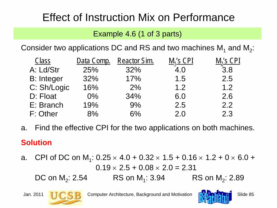
Effect of Instruction Mix on PerformanceExample 4.6 (1 of 3 parts)
Consider two applications DC and RS and two machines M1 and M2:
Class Data Comp. Reactor Sim. M1’s CPI M2’s CPIA: Ld/Str 25% 32% 4.0 3.8B: Integer 32% 17% 1.5 2.5C: Sh/Logic 16% 2% 1.2 1.2D: Float 0% 34% 6.0 2.6E: Branch 19% 9% 2.5 2.2F: Other 8% 6% 2.0 2.3
a. Find the effective CPI for the two applications on both machines.
Solution
a. CPI of DC on M1: 0.25 × 4.0 + 0.32 × 1.5 + 0.16 × 1.2 + 0 × 6.0 + 0.19 × 2.5 + 0.08 × 2.0 = 2.31
DC on M2: 2.54 RS on M1: 3.94 RS on M2: 2.89

Jan. 2011 Computer Architecture, Background and Motivation Slide 86
4.6 The Quest for Higher PerformanceState of available computing power ca. the early 2000s:
Gigaflops on the desktopTeraflops in the supercomputer centerPetaflops on the drawing board
Note on terminology (see Table 3.1)
Prefixes for large units:Kilo = 103, Mega = 106, Giga = 109, Tera = 1012, Peta = 1015
For memory:K = 210 = 1024, M = 220, G = 230, T = 240, P = 250
Prefixes for small units:micro = 10−6, nano = 10−9, pico = 10−12, femto = 10−15
Jan. 2011 Computer Architecture, Background and Motivation Slide 87
Figure 3.10 Trends in processor performance and DRAM memory chip capacity (Moore’s law).
Performance Trends and Obsolescence
1Mb
1990 1980 2000 2010 kIPS
MIPS
GIPS
TIPS
Pro
cess
or p
erfo
rman
ce
Calendar year
80286 68000
80386
80486
68040 Pentium
Pentium II R10000
×1.6 / yr
×10 / 5 yrs ×2 / 18 mos
64Mb
4Mb
64kb
256kb
256Mb
1Gb
16Mb
×4 / 3 yrs
Processor
Memory
kb
Mb
Gb
Tb
Mem
ory
chip
cap
acity
“Can I call you back? We just bought a new computer and we’re trying to set it up before it’s obsolete.”

Jan. 2011 Computer Architecture, Background and Motivation Slide 88
Figure 4.7 Exponential growth of supercomputer performance.
Super-computers
1990 1980 2000 2010
Sup
erco
mpu
ter p
erfo
rman
ce
Calendar year
Cray X-MP
Y-MP
CM-2
MFLOPS
GFLOPS
TFLOPS
PFLOPS
Vector supercomputers
CM-5
CM-5
$240M MPPs
$30M MPPs
Massively parallel processors
Jan. 2011 Computer Architecture, Background and Motivation Slide 89
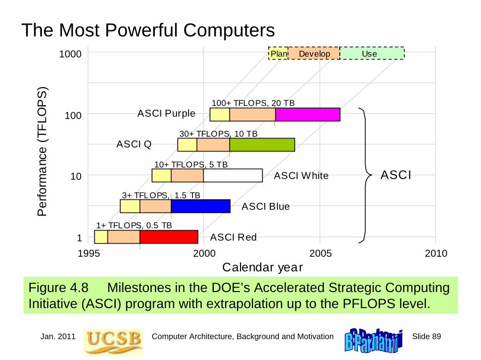
Figure 4.8 Milestones in the DOE’s Accelerated Strategic Computing Initiative (ASCI) program with extrapolation up to the PFLOPS level.
The Most Powerful Computers
2000 1995 2005 2010
Per
form
ance
(TFL
OP
S)
Calendar year
ASCI Red
ASCI Blue
ASCI White
1+ TFLOPS, 0.5 TB
3+ TFLOPS, 1.5 TB
10+ TFLOPS, 5 TB
30+ TFLOPS, 10 TB
100+ TFLOPS, 20 TB
1
10
100
1000 Plan Develop Use
ASCI
ASCI Purple
ASCI Q

Jan. 2011 Computer Architecture, Background and Motivation Slide 90
Figure 25.1 Trend in computational performance per watt of power used in general-purpose processors and DSPs.
Performance is Important, But It Isn’t Everything
1990 1980 2000 2010kIPS
MIPS
GIPS
TIPS
Per
form
ance
Calendar year
Absolute processor
performance
GP processor performance
per Watt
DSP performance per Watt

Jan. 2011 Computer Architecture, Background and Motivation Slide 91
Roadmap for the Rest of the BookCh. 5-8: A simple ISA, variations in ISA
Ch. 9-12: ALU design
Ch. 13-14: Data path and control unit designCh. 15-16: Pipelining and its limits
Ch. 17-20: Memory (main, mass, cache, virtual)
Ch. 21-24: I/O, buses, interrupts, interfacing
Fasten your seatbelts as we begin our ride!
Ch. 25-28: Vector and parallel processing

Jan. 2011 Computer Architecture, Instruction-Set Architecture Slide 1
Part IIInstruction-Set Architecture

Jan. 2011 Computer Architecture, Instruction-Set Architecture Slide 2
About This PresentationThis presentation is intended to support the use of the textbookComputer Architecture: From Microprocessors to Supercomputers, Oxford University Press, 2005, ISBN 0-19-515455-X. It is updated regularly by the author as part of his teaching of the upper-division course ECE 154, Introduction to Computer Architecture, at the University of California, Santa Barbara. Instructors can use these slides freely in classroom teaching and for other educational purposes. Any other use is strictly prohibited. © Behrooz Parhami
Edition Released Revised Revised Revised RevisedFirst June 2003 July 2004 June 2005 Mar. 2006 Jan. 2007
Jan. 2008 Jan. 2009 Jan. 2011
Jan. 2011 Computer Architecture, Instruction-Set Architecture Slide 3
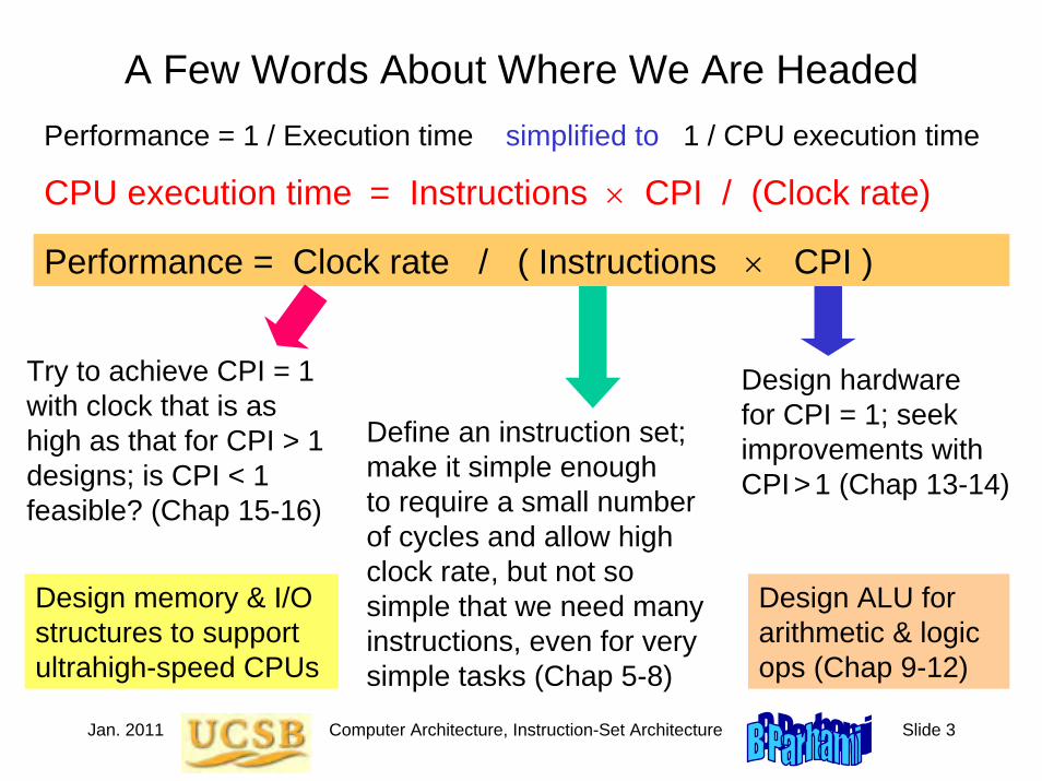
A Few Words About Where We Are HeadedPerformance = 1 / Execution time simplified to 1 / CPU execution time
CPU execution time = Instructions × CPI / (Clock rate)
Performance = Clock rate / ( Instructions × CPI )
Define an instruction set;make it simple enough to require a small number of cycles and allow high clock rate, but not so simple that we need many instructions, even for very simple tasks (Chap 5-8)
Design hardware for CPI = 1; seek improvements with CPI >1 (Chap 13-14)
Design ALU for arithmetic & logic ops (Chap 9-12)
Try to achieve CPI = 1 with clock that is as high as that for CPI > 1 designs; is CPI < 1 feasible? (Chap 15-16)
Design memory & I/O structures to support ultrahigh-speed CPUs

Jan. 2011 Computer Architecture, Instruction-Set Architecture Slide 4
Strategies for Speeding Up Instruction ExecutionPerformance = 1 / Execution time simplified to 1 / CPU execution time
CPU execution time = Instructions × CPI / (Clock rate)
Performance = Clock rate / ( Instructions × CPI )
Items that take longest to inspect dictate the speed of the assembly line
Assembly line analogy
Single-cycle (CPI = 1)
Multicycle (CPI > 1)
Faster
Parallel processing or pipelining
Faster

Jan. 2011 Computer Architecture, Instruction-Set Architecture Slide 5
II Instruction Set Architecture
Topics in This PartChapter 5 Instructions and AddressingChapter 6 Procedures and DataChapter 7 Assembly Language ProgramsChapter 8 Instruction Set Variations
Introduce machine “words” and its “vocabulary,” learning:• A simple, yet realistic and useful instruction set• Machine language programs; how they are executed• RISC vs CISC instruction-set design philosophy

Jan. 2011 Computer Architecture, Instruction-Set Architecture Slide 6
5 Instructions and Addressing
Topics in This Chapter
5.1 Abstract View of Hardware
5.2 Instruction Formats
5.3 Simple Arithmetic / Logic Instructions
5.4 Load and Store Instructions
5.5 Jump and Branch Instructions
5.6 Addressing Modes
First of two chapters on the instruction set of MiniMIPS:• Required for hardware concepts in later chapters• Not aiming for proficiency in assembler programming

Jan. 2011 Computer Architecture, Instruction-Set Architecture Slide 7
5.1 Abstract View of Hardware
Figure 5.1 Memory and processing subsystems for MiniMIPS.
Memory up to 2 words 30
Loc 0 Loc 4 Loc 8
Loc m − 4
Loc m − 8
4 B / location
m ≤ 2 32
$0 $1 $2
$31
Hi Lo
ALU
$0 $1 $2
$31 FP
arith
EPC Cause
BadVaddr Status
EIU FPU
TMU
Execution & integer unit
Floating- point unit
Trap & memory unit
. . .
. . .
(Coproc. 1)
(Coproc. 0)
(Main proc.)
Integer mul/div
Chapter 10
Chapter 11
Chapter 12

Jan. 2011 Computer Architecture, Instruction-Set Architecture Slide 8
Data Types
MiniMIPS registers hold 32-bit (4-byte) words. Other common data sizes include byte, halfword, and doubleword.
Byte
Halfword
Word
Doubleword
Byte = 8 bits
Word = 4 bytes
Doubleword = 8 bytes
Quadword (16 bytes) also used occasionally
Halfword = 2 bytesUsed only for floating-point data, so safe to ignore in this course
Jan. 2011 Computer Architecture, Instruction-Set Architecture Slide 9
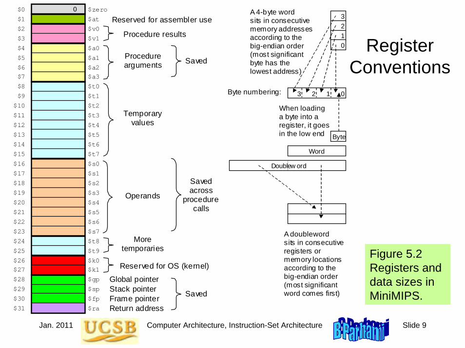
Register Conventions
Figure 5.2 Registers and data sizes in MiniMIPS.
Temporary values
More temporaries
Operands
Global pointer Stack pointer Frame pointer Return address
Saved
Saved Procedure arguments
Saved across
procedure calls
Procedure results
Reserved for assembler use
Reserved for OS (kernel)
$0 $1 $2 $3 $4 $5 $6 $7 $8 $9 $10 $11 $12 $13 $14 $15 $16 $17 $18 $19 $20 $21 $22 $23 $24 $25 $26 $27 $28 $29 $30 $31
0
$zero
$t0
$t2
$t4
$t6
$t1
$t3
$t5
$t7
$s0
$s2
$s4
$s6
$s1
$s3
$s5
$s7
$t8
$t9
$gp
$sp
$fp
$ra
$at
$k0
$k1
$v0
$a0
$a2
$v1
$a1
$a3
A doubleword sits in consecutive registers or memory locations according to the big-endian order (most significant word comes first)
When loading a byte into a register, it goes in the low end Byte
Word
Doublew ord
Byte numbering: 0 1 2 3
3 2 1 0
A 4-byte word sits in consecutive memory addresses according to the big-endian order (most significant byte has the lowest address)

Jan. 2011 Computer Architecture, Instruction-Set Architecture Slide 10
Registers Used in This Chapter
Figure 5.2 (partial)
Temporary values
More temporaries
Operands
Saved across
procedure calls
$8 $9 $10 $11 $12 $13 $14 $15 $16 $17 $18 $19 $20 $21 $22 $23 $24 $25
$t0
$t2
$t4
$t6
$t1
$t3
$t5
$t7
$s0
$s2
$s4
$s6
$s1
$s3
$s5
$s7
$t8
$t9
10 temporary registers
8 operand registers
WalletKeys
Change
Analogy for register usage conventions

Jan. 2011 Computer Architecture, Instruction-Set Architecture Slide 11
5.2 Instruction Formats
Figure 5.3 A typical instruction for MiniMIPS and steps in its execution.
Assembly language instruction:
Machine language instruction:
High-level language statement:
000000 10010 10001 11000 00000 100000
add $t8, $s2, $s1
a = b + c
ALU-type instruction
Register 18
Register 17
Register 24 Unused
Addition opcode
ALU
Instruction fetch
Register readout Operation Data
read/storeRegister
writeback
Register file
Instruction
cache
Data cache (not used)
Register file
P C
$17 $18
$24

Jan. 2011 Computer Architecture, Instruction-Set Architecture Slide 12
Add, Subtract, and Specification of Constants
MiniMIPS add & subtract instructions; e.g., compute: g = (b + c) − (e + f)
add $t8,$s2,$s3 # put the sum b + c in $t8add $t9,$s5,$s6 # put the sum e + f in $t9sub $s7,$t8,$t9 # set g to ($t8) − ($t9)
Decimal and hex constants
Decimal 25, 123456, −2873Hexadecimal 0x59, 0x12b4c6, 0xffff0000
Machine instruction typically contains
an opcodeone or more source operandspossibly a destination operand

Jan. 2011 Computer Architecture, Instruction-Set Architecture Slide 13
MiniMIPS Instruction Formats
Figure 5.4 MiniMIPS instructions come in only three formats:register (R), immediate (I), and jump (J).
5 bits 5 bits 31 25 20 15 0
Opcode Source register 1
Source register 2
op rs rt
R 6 bits 5 bits
rd
5 bits
sh
6 bits 10 5
fn
Destination register
Shift amount
Opcode extension
Imm ediate operand or address offset
31 25 20 15 0
Opcode Destination or data
Source or base
op rs rt operand / offset
I 5 bits 6 bits 16 bits 5 bits
0 0 0 0 0 0 0 0 0 0 0 1 1 1 1 1 1 0 0 0 0 0 0 0 0 0 31 0
Opcode
op jump target address
J Memory word address (byte address divided by 4)
26 bits 25
6 bits

Jan. 2011 Computer Architecture, Instruction-Set Architecture Slide 14
5.3 Simple Arithmetic/Logic Instructions
Figure 5.5 The arithmetic instructions add and sub have a format that is common to all two-operand ALU instructions. For these, the fn field specifies the arithmetic/logic operation to be performed.
0 0 0 0 0 0 0 0 0 0 0 0 0 0 0 1 x 0 0 1 1 1 1 0 0 0 0 0 0 0 0 0 31 25 20 15 0
ALU instruction
Source register 1
Source register 2
op rs rt
R rd sh
10 5 fn
Destination register
Unused add = 32 sub = 34
Add and subtract already discussed; logical instructions are similar add $t0,$s0,$s1 # set $t0 to ($s0)+($s1)sub $t0,$s0,$s1 # set $t0 to ($s0)-($s1)and $t0,$s0,$s1 # set $t0 to ($s0)∧($s1)or $t0,$s0,$s1 # set $t0 to ($s0)∨($s1)xor $t0,$s0,$s1 # set $t0 to ($s0)⊕($s1)nor $t0,$s0,$s1 # set $t0 to (($s0)∨($s1))′

Jan. 2011 Computer Architecture, Instruction-Set Architecture Slide 15
Arithmetic/Logic with One Immediate Operand
Figure 5.6 Instructions such as addi allow us to perform an arithmetic or logic operation for which one operand is a small constant.
0 0 0 0 0 0 0 0 0 0 0 0 0 0 1 1 1 1 1 0 0 1 1 0 0 0 0 0 0 0 0 31 25 20 15 0
addi = 8 Destination Source Immediate operand
op rs rt operand / offset
I 1
An operand in the range [−32 768, 32 767], or [0x0000, 0xffff], can be specified in the immediate field.
addi $t0,$s0,61 # set $t0 to ($s0)+61andi $t0,$s0,61 # set $t0 to ($s0)∧61ori $t0,$s0,61 # set $t0 to ($s0)∨61xori $t0,$s0,0x00ff # set $t0 to ($s0)⊕ 0x00ff
For arithmetic instructions, the immediate operand is sign-extended
1 0 0 1Errors

Jan. 2011 Computer Architecture, Instruction-Set Architecture Slide 16
5.4 Load and Store Instructions
Figure 5.7 MiniMIPS lw and sw instructions and their memory addressing convention that allows for simple access to array elements via a base address and an offset (offset = 4i leads us to the i th word).
0 0 0 0 0 0 0 0 0 0 0 0 1 0 0 x 1 0 0 0 0 0 0 31 25 20 15 0
lw = 35 sw = 43
Base register
Data register
Offset relative to base
op rs rt operand / offset
I 1 1 0 0 1 1 1 1 1
A[0] A[1] A[2]
A[i]
Address in base register
Offset = 4i
.
.
.
Memory
Element i of array A
Note on base and offset: The memory address is the sum of (rs) and an immediate value. Calling one of these the base and the other the offset is quite arbitrary. It would make perfect sense to interpret the address A($s3) as having the base A and the offset ($s3). However, a 16-bit base confines us to a small portion of memory space.
lw $t0,40($s3)lw $t0,A($s3)

Jan. 2011 Computer Architecture, Instruction-Set Architecture Slide 17
lw, sw, and lui Instructions
Figure 5.8 The lui instruction allows us to load an arbitrary 16-bit value into the upper half of a register while setting its lower half to 0s.
0
0 0 0 0 0 0 0 0 0 0 0 1 1 1 1 1 0 0 0 0 0 0 0 0 0 0 0 0 0 0 0 0
0 0 0 0 0 0 0 0 0 0 0 1 1 1 1 1 0 0 1 1 1 1 1 0 0 0 0 0 0 0 0 31 25 20 15 0
lui = 15 Destination Unused Immediate operand
op rs rt operand / offset
I
Content of $s0 after the instruction is executed
lw $t0,40($s3) # load mem[40+($s3)] in $t0sw $t0,A($s3) # store ($t0) in mem[A+($s3)]
# “($s3)” means “content of $s3”lui $s0,61 # The immediate value 61 is
# loaded in upper half of $s0# with lower 16b set to 0s
Jan. 2011 Computer Architecture, Instruction-Set Architecture Slide 18
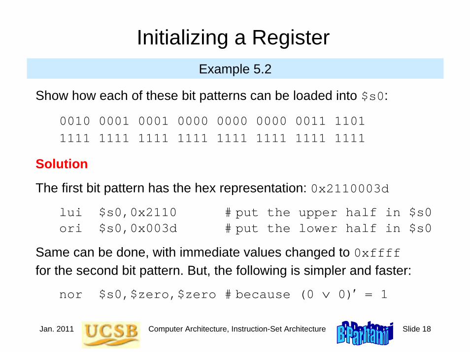
Initializing a RegisterExample 5.2
Show how each of these bit patterns can be loaded into $s0:
0010 0001 0001 0000 0000 0000 0011 11011111 1111 1111 1111 1111 1111 1111 1111
Solution
The first bit pattern has the hex representation: 0x2110003d
lui $s0,0x2110 # put the upper half in $s0 ori $s0,0x003d # put the lower half in $s0
Same can be done, with immediate values changed to 0xfffffor the second bit pattern. But, the following is simpler and faster:
nor $s0,$zero,$zero # because (0 ∨ 0)′ = 1
Jan. 2011 Computer Architecture, Instruction-Set Architecture Slide 19
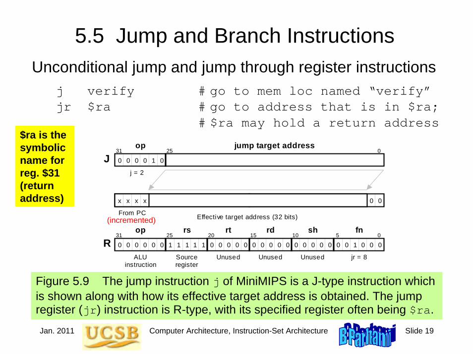
5.5 Jump and Branch InstructionsUnconditional jump and jump through register instructions
j verify # go to mem loc named “verify”jr $ra # go to address that is in $ra;
# $ra may hold a return address
Figure 5.9 The jump instruction j of MiniMIPS is a J-type instruction which is shown along with how its effective target address is obtained. The jump register (jr) instruction is R-type, with its specified register often being $ra.
0
0 0 0 0 0 0 0 1 1 1 1 1 0 0 0 0 0 0 0 0 0 0 0 0 0 0 0 0
0 0 0 0 0 0 0 0 0 0 0 1 1 1 1 1 0 0 1 0 0 0 0 0 0 0 0 0 31 0
j = 2
op jump target address
J
Effective target address (32 bits)
25
From PC
0 0
x x x x
0 0 0 1 1 1 1 0 0 0 0 0 0 0 0 0 0 0 0 0 0 0 0 0 0 0 1 1 0 0 0 0 31 25 20 15 0
ALU instruction
Source register
Unused
op rs rt
R rd sh
10 5 fn
Unused Unused jr = 8
$ra is the symbolic name for reg. $31 (return address)
(incremented)
Jan. 2011 Computer Architecture, Instruction-Set Architecture Slide 20
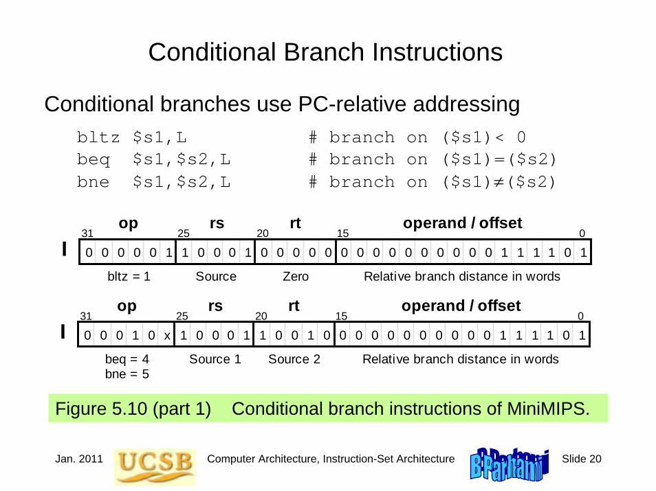
Conditional Branch Instructions
Figure 5.10 (part 1) Conditional branch instructions of MiniMIPS.
Conditional branches use PC-relative addressingbltz $s1,L # branch on ($s1)< 0beq $s1,$s2,L # branch on ($s1)=($s2)bne $s1,$s2,L # branch on ($s1)≠($s2)
0 1 0 0 0 0 0 0 0 0 0 0 0 0 0 0 1 1 1 1 1 0 0 1 1 0 0 0 0 0 0 31 25 20 15 0
bltz = 1 Zero Source Relative branch distance in words
op rs rt operand / offset
I 0
1 1 0 0 x 0 0 0 0 0 0 0 0 0 0 0 1 1 1 1 1 0 0 1 1 0 0 0 0 0 0 31 25 20 15 0
beq = 4 bne = 5
Source 2 Source 1 Relative branch distance in words
op rs rt operand / offset
I 1

Jan. 2011 Computer Architecture, Instruction-Set Architecture Slide 21
Comparison Instructions for Conditional Branching
Figure 5.10 (part 2) Comparison instructions of MiniMIPS.
slt $s1,$s2,$s3 # if ($s2)<($s3), set $s1 to 1 # else set $s1 to 0;# often followed by beq/bne
slti $s1,$s2,61 # if ($s2)<61, set $s1 to 1 # else set $s1 to 0
1 1 1 0 1 1 1 0 0 0 1 1 0 0 0 0 0 0 0 0 0 0 0 0 0 0 0 0 1 1 0 0 31 25 20 15 0
ALU instruction
Source 1 register
Source 2 register
op rs rt
R rd sh
10 5 fn
Destination Unused slt = 42
1 1 1 0 0 0 0 0 0 0 0 0 0 0 0 0 1 1 1 1 1 0 0 1 1 0 0 0 0 0 0 31 25 20 15 0
slti = 10 Destination Source Immediate operand
op rs rt operand / offset
I 1

Jan. 2011 Computer Architecture, Instruction-Set Architecture Slide 22
Examples for Conditional BranchingIf the branch target is too far to be reachable with a 16-bit offset (rare occurrence), the assembler automatically replaces the branch instruction beq $s0,$s1,L1 with:
bne $s1,$s2,L2 # skip jump if (s1)≠(s2)j L1 # goto L1 if (s1)=(s2)
L2: ...
Forming if-then constructs; e.g., if (i == j) x = x + y
bne $s1,$s2,endif # branch on i≠jadd $t1,$t1,$t2 # execute the “then” part
endif: ...
If the condition were (i < j), we would change the first line to:
slt $t0,$s1,$s2 # set $t0 to 1 if i<jbeq $t0,$0,endif # branch if ($t0)=0;
# i.e., i not< j or i≥j
Jan. 2011 Computer Architecture, Instruction-Set Architecture Slide 23
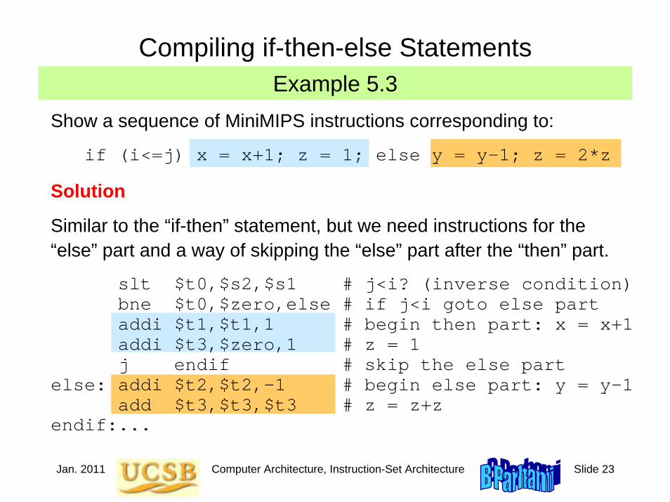
Example 5.3 Compiling if-then-else Statements
Show a sequence of MiniMIPS instructions corresponding to:
if (i<=j) x = x+1; z = 1; else y = y–1; z = 2*z
Solution
Similar to the “if-then” statement, but we need instructions for the“else” part and a way of skipping the “else” part after the “then” part.
slt $t0,$s2,$s1 # j<i? (inverse condition)bne $t0,$zero,else # if j<i goto else partaddi $t1,$t1,1 # begin then part: x = x+1addi $t3,$zero,1 # z = 1j endif # skip the else part
else: addi $t2,$t2,-1 # begin else part: y = y–1add $t3,$t3,$t3 # z = z+z
endif:...

Jan. 2011 Computer Architecture, Instruction-Set Architecture Slide 24
5.6 Addressing Modes
Figure 5.11 Schematic representation of addressing modes in MiniMIPS.
Addressing Instruction Other elements involved Operand
Implied
Immediate
Register
Base
PC-relative
Pseudodirect
Some place in the machine
Extend, if required
Reg f ile Reg spec Reg data
Memory Add
Reg file
Mem addr
Constant offset
Reg base Reg data
Mem data
Add
PC
Constant offset
Memory
Mem addr Mem
data
Memory Mem data
PC Mem addr
Incremented

Jan. 2011 Computer Architecture, Instruction-Set Architecture Slide 25
Example 5.5 List A is stored in memory beginning at the address given in $s1. List length is given in $s2. Find the largest integer in the list and copy it into $t0.
Solution
Scan the list, holding the largest element identified thus far in $t0.lw $t0,0($s1) # initialize maximum to A[0]addi $t1,$zero,0 # initialize index i to 0
loop: add $t1,$t1,1 # increment index i by 1beq $t1,$s2,done # if all elements examined, quitadd $t2,$t1,$t1 # compute 2i in $t2add $t2,$t2,$t2 # compute 4i in $t2 add $t2,$t2,$s1 # form address of A[i] in $t2 lw $t3,0($t2) # load value of A[i] into $t3slt $t4,$t0,$t3 # maximum < A[i]?beq $t4,$zero,loop # if not, repeat with no changeaddi $t0,$t3,0 # if so, A[i] is the new
maximum j loop # change completed; now repeat
done: ... # continuation of the program
Finding the Maximum Value in a List of Integers

Jan. 2011 Computer Architecture, Instruction-Set Architecture Slide 26
The 20 MiniMIPS Instructions
Covered So Far
Instruction UsageLoad upper immediate lui rt,imm
Add add rd,rs,rt
Subtract sub rd,rs,rt
Set less than slt rd,rs,rt
Add immediate addi rt,rs,imm
Set less than immediate slti rd,rs,imm
AND and rd,rs,rt
OR or rd,rs,rt
XOR xor rd,rs,rt
NOR nor rd,rs,rt
AND immediate andi rt,rs,imm
OR immediate ori rt,rs,imm
XOR immediate xori rt,rs,imm
Load word lw rt,imm(rs)
Store word sw rt,imm(rs)
Jump j L
Jump register jr rs
Branch less than 0 bltz rs,L
Branch equal beq rs,rt,L
Branch not equal bne rs,rt,L
Copy
Control transfer
Logic
Arithmetic
Memory access
op15
0008
100000
1213143543
20145
fn
323442
36373839
8
Table 5.1
5 bits 5 bits 31 25 20 15 0
Opcode Source register 1
Source register 2
op rs rt
R 6 bits 5 bits
rd
5 bits
sh
6 bits 10 5
fn
Destination register
Shift amount
Opcode extension
Immediate operand or address offset
31 25 20 15 0
Opcode Destination or data
Source or base
op rs rt operand / offset
I 5 bits 6 bits 16 bits 5 bits
0 0 0 0 0 0 0 0 0 0 0 1 1 1 1 1 1 0 0 0 0 0 0 0 0 0 31 0
Opcode
op jump target address
J Memory word address (byte address divided by 4)
26 bits 25
6 bits

Jan. 2011 Computer Architecture, Instruction-Set Architecture Slide 27
6 Procedures and Data
Topics in This Chapter
6.1 Simple Procedure Calls
6.2 Using the Stack for Data Storage
6.3 Parameters and Results
6.4 Data Types
6.5 Arrays and Pointers
6.6 Additional Instructions
Finish our study of MiniMIPS instructions and its data types:• Instructions for procedure call/return, misc. instructions• Procedure parameters and results, utility of stack

Jan. 2011 Computer Architecture, Instruction-Set Architecture Slide 28
6.1 Simple Procedure CallsUsing a procedure involves the following sequence of actions:
1. Put arguments in places known to procedure (reg’s $a0-$a3)2. Transfer control to procedure, saving the return address (jal)3. Acquire storage space, if required, for use by the procedure4. Perform the desired task5. Put results in places known to calling program (reg’s $v0-$v1)6. Return control to calling point (jr)
MiniMIPS instructions for procedure call and return from procedure:
jal proc # jump to loc “proc” and link;# “link” means “save the return# address” (PC)+4 in $ra ($31)
jr rs # go to loc addressed by rs
Jan. 2011 Computer Architecture, Instruction-Set Architecture Slide 29
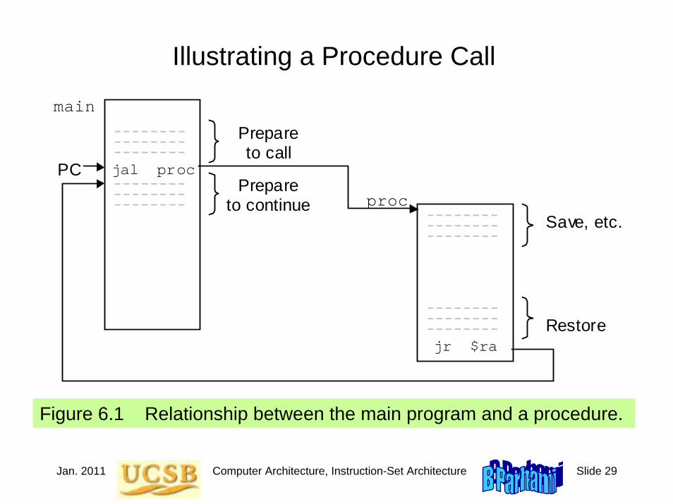
Illustrating a Procedure Call
Figure 6.1 Relationship between the main program and a procedure.
jal proc
jr $ra
proc Save, etc.
Restore
PC Prepare
to continue
Prepare to call
main

Jan. 2011 Computer Architecture, Instruction-Set Architecture Slide 30
Recalling Register
Conventions
Figure 5.2 Registers and data sizes in MiniMIPS.
Temporary values
More temporaries
Operands
Global pointer Stack pointer Frame pointer Return address
Saved
Saved Procedure arguments
Saved across
procedure calls
Procedure results
Reserved for assembler use
Reserved for OS (kernel)
$0 $1 $2 $3 $4 $5 $6 $7 $8 $9 $10 $11 $12 $13 $14 $15 $16 $17 $18 $19 $20 $21 $22 $23 $24 $25 $26 $27 $28 $29 $30 $31
0
$zero
$t0
$t2
$t4
$t6
$t1
$t3
$t5
$t7
$s0
$s2
$s4
$s6
$s1
$s3
$s5
$s7
$t8
$t9
$gp
$sp
$fp
$ra
$at
$k0
$k1
$v0
$a0
$a2
$v1
$a1
$a3
A doubleword sits in consecutive registers or memory locations according to the big-endian order (most significant word comes first)
When loading a byte into a register, it goes in the low end Byte
Word
Doublew ord
Byte numbering: 0 1 2 3
3 2 1 0
A 4-byte word sits in consecutive memory addresses according to the big-endian order (most significant byte has the lowest address)

Jan. 2011 Computer Architecture, Instruction-Set Architecture Slide 31
Example 6.1 A Simple MiniMIPS Procedure
Procedure to find the absolute value of an integer.
$v0 ← |($a0)|
Solution
The absolute value of x is –x if x < 0 and x otherwise.
abs: sub $v0,$zero,$a0 # put -($a0) in $v0; # in case ($a0) < 0
bltz $a0,done # if ($a0)<0 then done add $v0,$a0,$zero # else put ($a0) in $v0
done: jr $ra # return to calling program
In practice, we seldom use such short procedures because of the overhead that they entail. In this example, we have 3-4 instructions of overhead for 3 instructions of useful computation.

Jan. 2011 Computer Architecture, Instruction-Set Architecture Slide 32
Nested Procedure Calls
Figure 6.2 Example of nested procedure calls.
jal abc
jr $ra
abc Save
Restore
PC Prepare to continue
Prepare to call
main
jal xyz
jr $ra
xyz
Procedure abc
Procedure xyz
Text version is incorrect

Jan. 2011 Computer Architecture, Instruction-Set Architecture Slide 33
6.2 Using the Stack for Data Storage
Figure 6.4 Effects of push and pop operations on a stack.
b a
sp
b a
sp b a sp
c
Push c Pop x
sp = sp – 4 mem[sp] = c
x = mem[sp]sp = sp + 4
push: addi $sp,$sp,-4sw $t4,0($sp)
pop: lw $t5,0($sp)addi $sp,$sp,4
Analogy:Cafeteria stack of plates/trays

Jan. 2011 Computer Architecture, Instruction-Set Architecture Slide 34
Memory Map in
MiniMIPS
Figure 6.3 Overview of the memory address space in MiniMIPS.
Reserved
Program
Stack
1 M words
Hex address
10008000
1000ffff
10000000
00000000
00400000
7ffffffc
Text segment 63 M words
Data segment
Stack segment
Static data
Dynamic data
$gp
$sp
$fp
448 M words
Second half of address space reserved for memory-mapped I/O
$28 $29 $30
Addressable with 16-bit signed offset
80000000
Jan. 2011 Computer Architecture, Instruction-Set Architecture Slide 35
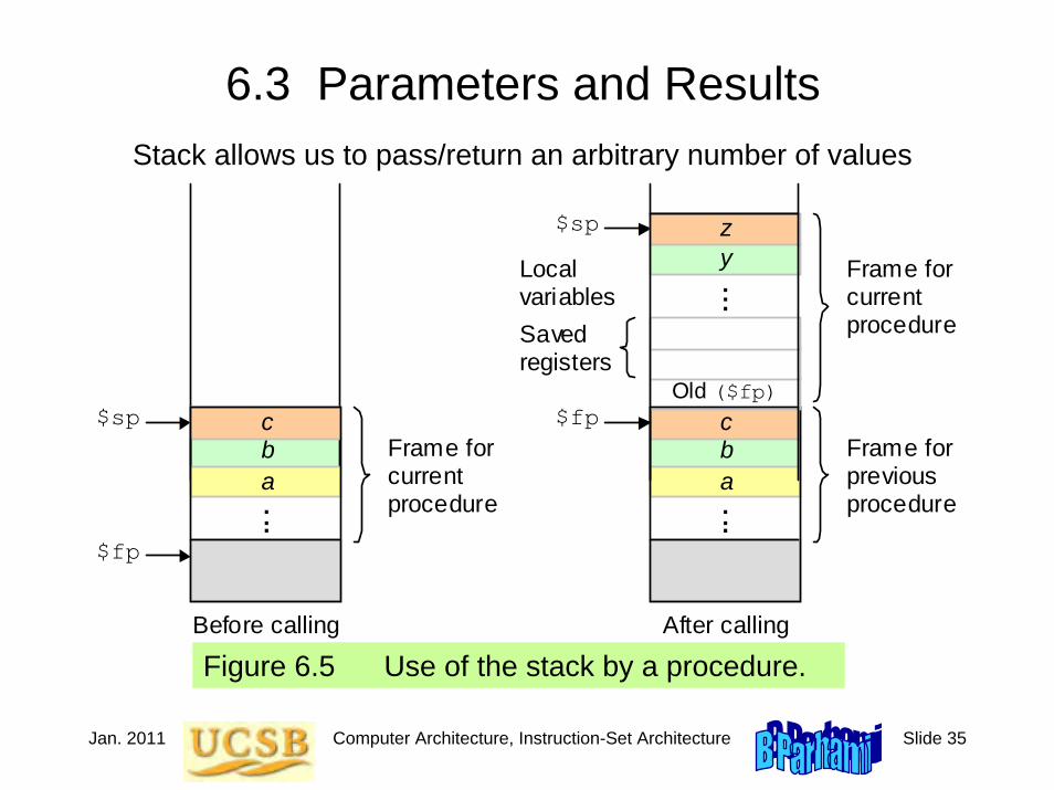
6.3 Parameters and Results
Figure 6.5 Use of the stack by a procedure.
b a
$sp c Frame for current procedure
$fp
. . .
Before calling
b a
$sp
c Frame for previous procedure
$fp
. . .
After calling
Frame for current procedure
Old ($fp)
Saved registers
y z
. . . Local variables
Stack allows us to pass/return an arbitrary number of values
Jan. 2011 Computer Architecture, Instruction-Set Architecture Slide 36
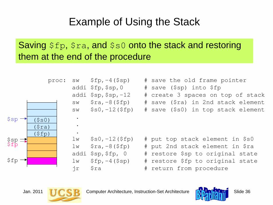
Example of Using the Stack
proc: sw $fp,-4($sp) # save the old frame pointeraddi $fp,$sp,0 # save ($sp) into $fpaddi $sp,$sp,–12 # create 3 spaces on top of stacksw $ra,-8($fp) # save ($ra) in 2nd stack elementsw $s0,-12($fp) # save ($s0) in top stack element...lw $s0,-12($fp) # put top stack element in $s0lw $ra,-8($fp) # put 2nd stack element in $raaddi $sp,$fp, 0 # restore $sp to original statelw $fp,-4($sp) # restore $fp to original statejr $ra # return from procedure
Saving $fp, $ra, and $s0 onto the stack and restoring them at the end of the procedure
$fp
$sp($fp)
$fp
$sp($ra)($s0)

Jan. 2011 Computer Architecture, Instruction-Set Architecture Slide 37
6.4 Data Types
Data size (number of bits), data type (meaning assigned to bits)
Signed integer: byte wordUnsigned integer: byte wordFloating-point number: word doublewordBit string: byte word doubleword
Converting from one size to anotherType 8-bit number Value 32-bit version of the number
Unsigned 0010 1011 43 0000 0000 0000 0000 0000 0000 0010 1011Unsigned 1010 1011 171 0000 0000 0000 0000 0000 0000 1010 1011
Signed 0010 1011 +43 0000 0000 0000 0000 0000 0000 0010 1011Signed 1010 1011 –85 1111 1111 1111 1111 1111 1111 1010 1011

Jan. 2011 Computer Architecture, Instruction-Set Architecture Slide 38
ASCII CharactersTable 6.1 ASCII (American standard code for information interchange)
NUL DLE SP 0 @ P ` pSOH DC1 ! 1 A Q a qSTX DC2 “ 2 B R b rETX DC3 # 3 C S c sEOT DC4 $ 4 D T d tENQ NAK % 5 E U e uACK SYN & 6 F V f vBEL ETB ‘ 7 G W g wBS CAN ( 8 H X h xHT EM ) 9 I Y i yLF SUB * : J Z j zVT ESC + ; K [ k {FF FS , < L \ l |CR GS - = M ] m }SO RS . > N ^ n ~SI US / ? O _ o DEL
0123456789abcdef
0 1 2 3 4 5 6 7 8-9 a-f
Morecontrols
Moresymbols
8-bit ASCII code(col #, row #)hex
e.g., code for + is (2b) hex or(0010 1011)two

Jan. 2011 Computer Architecture, Instruction-Set Architecture Slide 39
Loading and Storing Bytes
Figure 6.6 Load and store instructions for byte-size data elements.
x x 0 0 0 0 0 0 0 0 0 0 0 0 0 1 0 0 1 0 0 0 0 0 0 31 25 20 15 0
lb = 32 lbu = 36 sb = 40
Data register
Base register
Address offset
op rs rt immediate / offset
I 1 1 0 0 0 1 1
Bytes can be used to store ASCII characters or small integers. MiniMIPS addresses refer to bytes, but registers hold words.
lb $t0,8($s3) # load rt with mem[8+($s3)]# sign-extend to fill reg
lbu $t0,8($s3) # load rt with mem[8+($s3)]# zero-extend to fill reg
sb $t0,A($s3) # LSB of rt to mem[A+($s3)]
Jan. 2011 Computer Architecture, Instruction-Set Architecture Slide 40
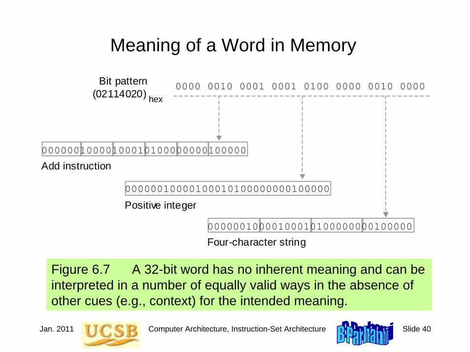
Meaning of a Word in Memory
Figure 6.7 A 32-bit word has no inherent meaning and can be interpreted in a number of equally valid ways in the absence of other cues (e.g., context) for the intended meaning.
0000 0010 0001 0001 0100 0000 0010 0000
Positive integer
Four-character string
Add instruction
Bit pattern (02114020) hex
00000010000100010100000000100000
00000010000100010100000000100000
00000010000100010100000000100000
Jan. 2011 Computer Architecture, Instruction-Set Architecture Slide 41
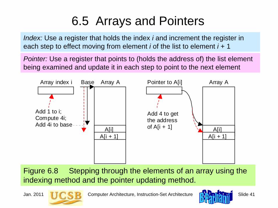
6.5 Arrays and PointersIndex: Use a register that holds the index i and increment the register in each step to effect moving from element i of the list to element i + 1
Pointer: Use a register that points to (holds the address of) the list element being examined and update it in each step to point to the next element
Add 4 to get the address of A[i + 1]
Pointer to A[i] Array index i
Add 1 to i; Compute 4i; Add 4i to base
A[i] A[i + 1]
A[i] A[i + 1]
Base Array A Array A
Figure 6.8 Stepping through the elements of an array using the indexing method and the pointer updating method.

Jan. 2011 Computer Architecture, Instruction-Set Architecture Slide 42
Selection SortExample 6.4
Figure 6.9 One iteration of selection sort.
first
last
max
first
last
first
last
Start of iteration Maximum identified End of iteration
x
x y
y
A A A
To sort a list of numbers, repeatedly perform the following:Find the max element, swap it with the last item, move up the “last” pointer

Jan. 2011 Computer Architecture, Instruction-Set Architecture Slide 43
Selection Sort Using the Procedure maxExample 6.4 (continued)
sort: beq $a0,$a1,done # single-element list is sortedjal max # call the max procedurelw $t0,0($a1) # load last element into $t0sw $t0,0($v0) # copy the last element to max locsw $v1,0($a1) # copy max value to last elementaddi $a1,$a1,-4 # decrement pointer to last elementj sort # repeat sort for smaller list
done: ... # continue with rest of program
first
last
max
first
last
first
last
Start of iteration Maximum identified End of iteration
x
x y
y
A A A
Inputs toproc max
Outputs fromproc max
In $a0
In $a1
In $v0 In $v1
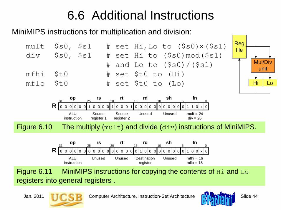
Jan. 2011 Computer Architecture, Instruction-Set Architecture Slide 44
6.6 Additional Instructions
Figure 6.10 The multiply (mult) and divide (div) instructions of MiniMIPS.
1 0 0 1 1 0 0
fn
0 0 0 0 0 0 0 0 0 0 0 0 x 0 0 1 1 0 0 0 0 0 0 0 0 31 25 20 15 0
ALU instruction
Source register 1
Source register 2
op rs rt
R rd sh
10 5
Unused Unused mult = 24 div = 26
1 0 0 0 0 0 0 1 0 0
fn
0 0 0 0 0 0 0 0 0 0 0 x 0 0 0 0 0 0 0 0 0 0 31 25 20 15 0
ALU instruction
Unused Unused
op rs rt
R rd sh
10 5
Destination register
Unused mfhi = 16 mflo = 18
Figure 6.11 MiniMIPS instructions for copying the contents of Hi and Loregisters into general registers .
MiniMIPS instructions for multiplication and division:
mult $s0, $s1 # set Hi,Lo to ($s0)×($s1)div $s0, $s1 # set Hi to ($s0)mod($s1)
# and Lo to ($s0)/($s1)mfhi $t0 # set $t0 to (Hi)mflo $t0 # set $t0 to (Lo)
Regfile
Mul/Divunit
Hi Lo

Jan. 2011 Computer Architecture, Instruction-Set Architecture Slide 45
Logical Shifts
Figure 6.12 The four logical shift instructions of MiniMIPS.
MiniMIPS instructions for left and right shifting:
sll $t0,$s1,2 # $t0=($s1) left-shifted by 2srl $t0,$s1,2 # $t0=($s1) right-shifted by 2sllv $t0,$s1,$s0 # $t0=($s1) left-shifted by ($s0)srlv $t0,$s1,$s0 # $t0=($s1) right-shifted by ($s0)
0
x
0 0
fn
0 0 0 0 0 0 0 0 0 0 0 1 0 0 x 0 0 1 1 1 0 0 0 0 0 0 0 0 0 31 25 20 15 0
ALU instruction
Unused Source register
op rs rt
R rd sh
10 5
Destination register
Shift amount
sll = 0 srl = 2
1 0 0 0 0 0 0 0 0 0 0 0 0 0 0 0 0 0 1 1 1 1 0 0 0 0 0 0 0 0 0 31 25 20 15 0
ALU instruction
Amount register
Source register
op rs rt
R rd sh
10 5 fn
Destination register
Unused sllv = 4 srlv = 6

Jan. 2011 Computer Architecture, Instruction-Set Architecture Slide 46
Unsigned Arithmetic and Miscellaneous Instructions
MiniMIPS instructions for unsigned arithmetic (no overflow exception):
addu $t0,$s0,$s1 # set $t0 to ($s0)+($s1)subu $t0,$s0,$s1 # set $t0 to ($s0)–($s1)multu $s0,$s1 # set Hi,Lo to ($s0)×($s1)divu $s0,$s1 # set Hi to ($s0)mod($s1)
# and Lo to ($s0)/($s1)addiu $t0,$s0,61 # set $t0 to ($s0)+61;
# the immediate operand is# sign extended
To make MiniMIPS more powerful and complete, we introduce later:
sra $t0,$s1,2 # sh. right arith (Sec. 10.5)srav $t0,$s1,$s0 # shift right arith variablesyscall # system call (Sec. 7.6)
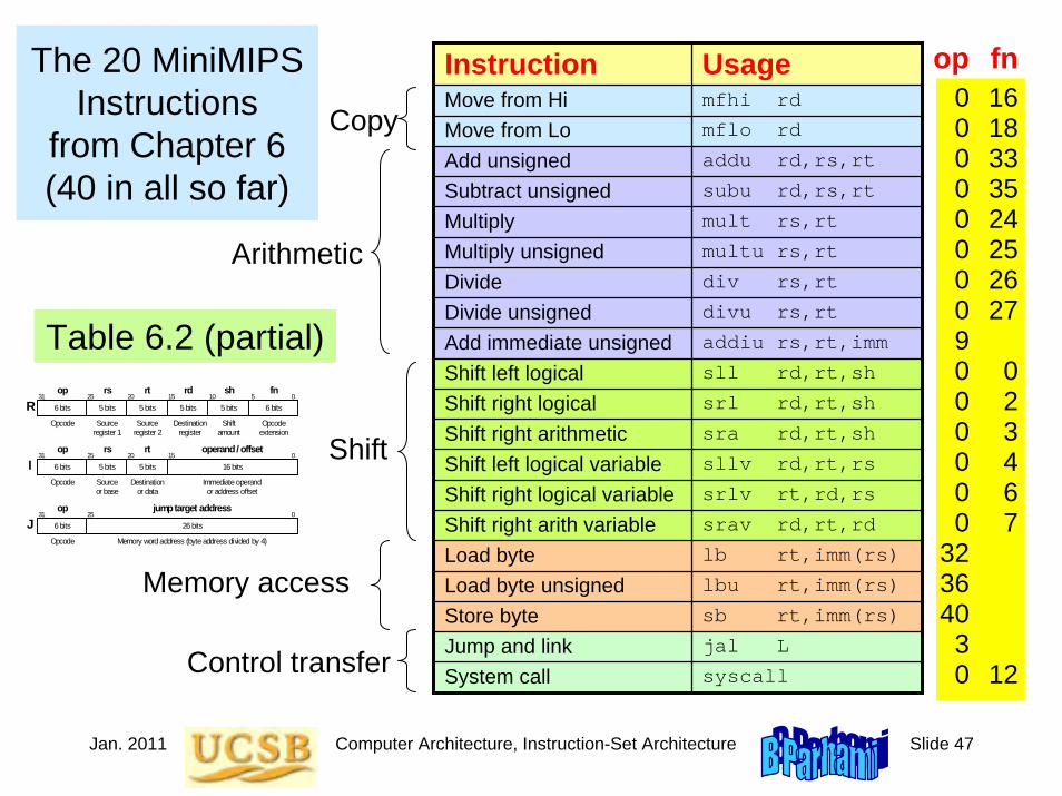
Jan. 2011 Computer Architecture, Instruction-Set Architecture Slide 47
The 20 MiniMIPS Instructions
from Chapter 6(40 in all so far)
Instruction UsageMove from Hi mfhi rd
Move from Lo mflo rd
Add unsigned addu rd,rs,rt
Subtract unsigned subu rd,rs,rt
Multiply mult rs,rt
Multiply unsigned multu rs,rt
Divide div rs,rt
Divide unsigned divu rs,rt
Add immediate unsigned addiu rs,rt,imm
Shift left logical sll rd,rt,sh
Shift right logical srl rd,rt,sh
Shift right arithmetic sra rd,rt,sh
Shift left logical variable sllv rd,rt,rs
Shift right logical variable srlv rt,rd,rs
Shift right arith variable srav rd,rt,rd
Load byte lb rt,imm(rs)
Load byte unsigned lbu rt,imm(rs)
Store byte sb rt,imm(rs)
Jump and link jal L
System call syscall
Copy
Control transfer
Shift
Arithmetic
Memory access
op000000009000000
323640
30
fn1618333524252627
023467
12
Table 6.2 (partial)
5 bits 5 bits 31 25 20 15 0
Opcode Source register 1
Source register 2
op rs rt
R 6 bits 5 bits
rd
5 bits
sh
6 bits 10 5
fn
Destination register
Shift amount
Opcode extension
Immediate operand or address offset
31 25 20 15 0
Opcode Destination or data
Source or base
op rs rt operand / offset
I 5 bits 6 bits 16 bits 5 bits
0 0 0 0 0 0 0 0 0 0 0 1 1 1 1 1 1 0 0 0 0 0 0 0 0 0 31 0
Opcode
op jump target address
J Memory word address (byte address divided by 4)
26 bits 25
6 bits

Jan. 2011 Computer Architecture, Instruction-Set Architecture Slide 48
Table 6.2 The 37 + 3 MiniMIPS Instructions Covered So FarInstruction UsageMove from Hi mfhi rd
Move from Lo mflo rd
Add unsigned addu rd,rs,rt
Subtract unsigned subu rd,rs,rt
Multiply mult rs,rt
Multiply unsigned multu rs,rt
Divide div rs,rt
Divide unsigned divu rs,rt
Add immediate unsigned addiu rs,rt,imm
Shift left logical sll rd,rt,sh
Shift right logical srl rd,rt,sh
Shift right arithmetic sra rd,rt,sh
Shift left logical variable sllv rd,rt,rs
Shift right logical variable srlv rd,rt,rs
Shift right arith variable srav rd,rt,rs
Load byte lb rt,imm(rs)
Load byte unsigned lbu rt,imm(rs)
Store byte sb rt,imm(rs)
Jump and link jal L
System call syscall
Instruction UsageLoad upper immediate lui rt,imm
Add add rd,rs,rt
Subtract sub rd,rs,rt
Set less than slt rd,rs,rt
Add immediate addi rt,rs,imm
Set less than immediate slti rd,rs,imm
AND and rd,rs,rt
OR or rd,rs,rt
XOR xor rd,rs,rt
NOR nor rd,rs,rt
AND immediate andi rt,rs,imm
OR immediate ori rt,rs,imm
XOR immediate xori rt,rs,imm
Load word lw rt,imm(rs)
Store word sw rt,imm(rs)
Jump j L
Jump register jr rs
Branch less than 0 bltz rs,L
Branch equal beq rs,rt,L
Branch not equal bne rs,rt,L
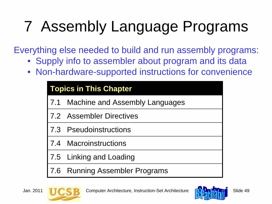
Jan. 2011 Computer Architecture, Instruction-Set Architecture Slide 49
7 Assembly Language Programs
Topics in This Chapter
7.1 Machine and Assembly Languages
7.2 Assembler Directives
7.3 Pseudoinstructions
7.4 Macroinstructions
7.5 Linking and Loading
7.6 Running Assembler Programs
Everything else needed to build and run assembly programs:• Supply info to assembler about program and its data• Non-hardware-supported instructions for convenience

Jan. 2011 Computer Architecture, Instruction-Set Architecture Slide 50
7.1 Machine and Assembly Languages
Figure 7.1 Steps in transforming an assembly language program to an executable program residing in memory.
Link
er
Load
er
Ass
embl
er
add $2,$5,$5 add $2,$2,$2 add $2,$4,$2 lw $15,0($2) lw $16,4($2) sw $16,0($2) sw $15,4($2) jr $31
00a51020 00421020 00821020 8c620000 8cf20004 acf20000 ac620004 03e00008
Assembly language program
Machine language program
Executable machine language program
Memory content
Library routines (machine language)
MIPS, 80x86, PowerPC, etc.

Jan. 2011 Computer Architecture, Instruction-Set Architecture Slide 51
Symbol Table
Figure 7.2 An assembly-language program, its machine-language version, and the symbol table created during the assembly process.
0 00100000000100000000000000001001
addi $s0,$zero,9
test
done result
12
28 248
4 00000010000100000100000000100010 8 00000001001000000000000000100000 12 00010101000100000000000000001100 16 00100001000010000000000000000001 20 00000010000000000100100000100000 24 00001000000000000000000000000011 28 10101111100010010000000011111000
Determined from assembler directives not shown here
Symbol table
done: sw $t1,result($gp)
sub $t0,$s0,$s0 add $t1,$zero,$zero
test: bne $t0,$s0,done
addi $t0,$t0,1 add $t1,$s0,$zero
j test
Assembly language program Machine language program Location
op rs rt rd sh fn Field boundaries shown to facilitate understanding

Jan. 2011 Computer Architecture, Instruction-Set Architecture Slide 52
7.2 Assembler DirectivesAssembler directives provide the assembler with info on how to translatethe program but do not lead to the generation of machine instructions
.macro # start macro (see Section 7.4)
.end_macro # end macro (see Section 7.4)
.text # start program’s text segment
... # program text goes here
.data # start program’s data segmenttiny: .byte 156,0x7a # name & initialize data byte(s)max: .word 35000 # name & initialize data word(s)
small: .float 2E-3 # name short float (see Chapter 12)big: .double 2E-3 # name long float (see Chapter 12)
.align 2 # align next item on word boundaryarray: .space 600 # reserve 600 bytes = 150 wordsstr1: .ascii “a*b” # name & initialize ASCII string str2: .asciiz “xyz” # null-terminated ASCII string
.global main # consider “main” a global name

Jan. 2011 Computer Architecture, Instruction-Set Architecture Slide 53
Composing Simple Assembler Directives
Write assembler directive to achieve each of the following objectives:
a. Put the error message “Warning: The printer is out of paper!” in memory.b. Set up a constant called “size” with the value 4.c. Set up an integer variable called “width” and initialize it to 4.d. Set up a constant called “mill” with the value 1,000,000 (one million).e. Reserve space for an integer vector “vect” of length 250.
Solution:
a. noppr: .asciiz “Warning: The printer is out of paper!”b. size: .byte 4 # small constant fits in one bytec. width: .word 4 # byte could be enough, but ...d. mill: .word 1000000 # constant too large for bytee. vect: .space 1000 # 250 words = 1000 bytes
Example 7.1

Jan. 2011 Computer Architecture, Instruction-Set Architecture Slide 54
7.3 Pseudoinstructions
Example of one-to-one pseudoinstruction: The followingnot $s0 # complement ($s0)
is converted to the real instruction:nor $s0,$s0,$zero # complement ($s0)
Example of one-to-several pseudoinstruction: The followingabs $t0,$s0 # put |($s0)| into $t0
is converted to the sequence of real instructions:add $t0,$s0,$zero # copy x into $t0slt $at,$t0,$zero # is x negative?beq $at,$zero,+4 # if not, skip next instrsub $t0,$zero,$s0 # the result is 0 – x
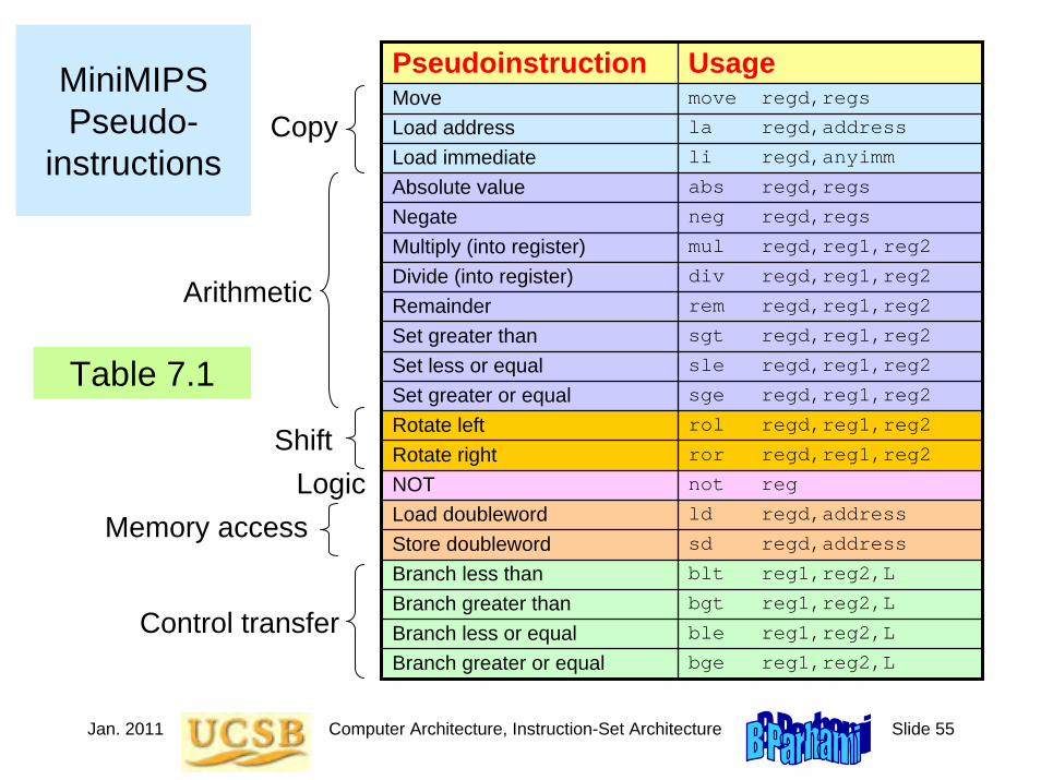
Jan. 2011 Computer Architecture, Instruction-Set Architecture Slide 55
MiniMIPS Pseudo-
instructions
Pseudoinstruction UsageMove move regd,regs
Load address la regd,address
Load immediate li regd,anyimm
Absolute value abs regd,regs
Negate neg regd,regs
Multiply (into register) mul regd,reg1,reg2
Divide (into register) div regd,reg1,reg2
Remainder rem regd,reg1,reg2
Set greater than sgt regd,reg1,reg2
Set less or equal sle regd,reg1,reg2
Set greater or equal sge regd,reg1,reg2
Rotate left rol regd,reg1,reg2
Rotate right ror regd,reg1,reg2
NOT not reg
Load doubleword ld regd,address
Store doubleword sd regd,address
Branch less than blt reg1,reg2,L
Branch greater than bgt reg1,reg2,L
Branch less or equal ble reg1,reg2,L
Branch greater or equal bge reg1,reg2,L
Copy
Control transfer
Shift
Arithmetic
Memory access
Table 7.1
Logic

Jan. 2011 Computer Architecture, Instruction-Set Architecture Slide 56
7.4 MacroinstructionsA macro is a mechanism to give a name to an often-used sequence of instructions (shorthand notation)
.macro name(args) # macro and arguments named
... # instr’s defining the macro
.end_macro # macro terminator
How is a macro different from a pseudoinstruction?Pseudos are predefined, fixed, and look like machine instructionsMacros are user-defined and resemble procedures (have arguments)
How is a macro different from a procedure?Control is transferred to and returns from a procedureAfter a macro has been replaced, no trace of it remains

Jan. 2011 Computer Architecture, Instruction-Set Architecture Slide 57
Macro to Find the Largest of Three Values
Write a macro to determine the largest of three values in registers and to put the result in a fourth register.
Solution:
.macro mx3r(m,a1,a2,a3) # macro and arguments namedmove m,a1 # assume (a1) is largest; m = (a1)bge m,a2,+4 # if (a2) is not larger, ignore itmove m,a2 # else set m = (a2)bge m,a3,+4 # if (a3) is not larger, ignore itmove m,a3 # else set m = (a3).endmacro # macro terminator
If the macro is used as mx3r($t0,$s0,$s4,$s3), the assembler replaces the arguments m, a1, a2, a3 with $t0, $s0, $s4, $s3, respectively.
Example 7.4

Jan. 2011 Computer Architecture, Instruction-Set Architecture Slide 58
7.5 Linking and Loading
The linker has the following responsibilities:Ensuring correct interpretation (resolution) of labels in all modulesDetermining the placement of text and data segments in memoryEvaluating all data addresses and instruction labelsForming an executable program with no unresolved references
The loader is in charge of the following:Determining the memory needs of the program from its headerCopying text and data from the executable program file into memoryModifying (shifting) addresses, where needed, during copyingPlacing program parameters onto the stack (as in a procedure call)Initializing all machine registers, including the stack pointerJumping to a start-up routine that calls the program’s main routine

Jan. 2011 Computer Architecture, Instruction-Set Architecture Slide 59
7.6 Running Assembler Programs
Spim is a simulator that can run MiniMIPS programs
The name Spim comes from reversing MIPS
Three versions of Spim are available for free downloading:
PCSpim for Windows machinesxspim for X-windowsspim for Unix systems
You can download SPIM from:
http://www.cs.wisc.edu/~larus/spim.html
SPIMA MIPS32 Simulator
James [email protected]
Microsoft ResearchFormerly: Professor, CS Dept., Univ. Wisconsin-Madison
spim is a self-contained simulator that will run MIPS32 assembly language programs. It reads and executes assembly . . .

Jan. 2011 Computer Architecture, Instruction-Set Architecture Slide 60
Input/Output Conventions for MiniMIPSTable 7.2 Input/output and control functions of syscall in PCSpim.
($v0) Function Arguments Result1 Print integer Integer in $a0 Integer displayed2 Print floating-point Float in $f12 Float displayed3 Print double-float Double-float in $f12,$f13 Double-float displayed4 Print string Pointer in $a0 Null-terminated string displayed5 Read integer Integer returned in $v0
6 Read floating-point Float returned in $f0
7 Read double-float Double-float returned in $f0,$f1
8 Read string Pointer in $a0, length in $a1 String returned in buffer at pointer9 Allocate memory Number of bytes in $a0 Pointer to memory block in $v0
10 Exit from program Program execution terminated
Out
put
Inpu
tC
ntl

Jan. 2011 Computer Architecture, Instruction-Set Architecture Slide 61
Figure 7.3
PCSpim User
Interface
Status bar
Menu bar Tools bar
File
Simulator
Window
Open Sav e Log File Ex it
Tile 1 Messages 2 Tex t Segment 3 Data Segment 4 Registers 5 Console Clear Console Toolbar Status bar
Clear Registers Reinitialize Reload Go Break Continue Single Step Multiple Step ... Breakpoints ... Set Value ... Disp Symbol Table Settings ...
For Help, press F1
PCSpim
Registers
File Simulator Window Help
PC = 00400000 EPC = 00000000 Cause = 00000000 Status = 00000000 HI = 00000000 LO = 00000000 General Registers R0 (r0) = 0 R8 (t0) = 0 R16 (s0) = 0 R24 R1 (at) = 0 R9 (t1) = 0 R17 (s1) = 0 R25
[0x00400000] 0x0c100008 jal 0x00400020 [main] ; 43 [0x00400004] 0x00000021 addu $0, $0, $0 ; 44 [0x00400008] 0x2402000a addiu $2, $0, 10 ; 45 [0x0040000c] 0x0000000c syscall ; 46 [0x00400010] 0x00000021 addu $0, $0, $0 ; 47
DATA [0x10000000] 0x00000000 0x6c696146 0x20206465 [0x10000010] 0x676e6974 0x44444120 0x6554000a [0x10000020] 0x44412067 0x000a4944 0x74736554
Text Segment
Data Segment
Messages
Base=1; Pseudo=1, Mapped=1; LoadTrap=0
?
?
See the file README for a full copyright notice. Memory and registers have been cleared, and the simulator rei D:\temp\dos\TESTS\Alubare.s has been successfully loaded

Jan. 2011 Computer Architecture, Instruction-Set Architecture Slide 62
8 Instruction Set Variations
Topics in This Chapter
8.1 Complex Instructions
8.2 Alternative Addressing Modes
8.3 Variations in Instruction Formats
8.4 Instruction Set Design and Evolution
8.5 The RISC/CISC Dichotomy
8.6 Where to Draw the Line
The MiniMIPS instruction set is only one example• How instruction sets may differ from that of MiniMIPS• RISC and CISC instruction set design philosophies
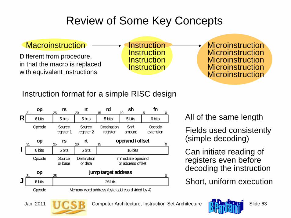
Jan. 2011 Computer Architecture, Instruction-Set Architecture Slide 63
Review of Some Key Concepts
Different from procedure, in that the macro is replaced with equivalent instructions
All of the same lengthFields used consistently (simple decoding)Can initiate reading of registers even before decoding the instructionShort, uniform execution
MacroinstructionInstructionInstructionInstruction
Instruction format for a simple RISC design
5 bits 5 bits 31 25 20 15 0
Opcode Source register 1
Source register 2
op rs rt
R 6 bits 5 bits
rd
5 bits
sh
6 bits 10 5
fn
Destination register
Shift amount
Opcode extension
Immediate operand or address offset
31 25 20 15 0
Opcode Destination or data
Source or base
op rs rt operand / offset
I 5 bits 6 bits 16 bits 5 bits
0 0 0 0 0 0 0 0 0 0 0 1 1 1 1 1 1 0 0 0 0 0 0 0 0 0 31 0
Opcode
op jump target address
J Memory word address (byte address divided by 4)
26 bits 25
6 bits
MicroinstructionMicroinstructionMicroinstructionMicroinstructionMicroinstruction
Instruction
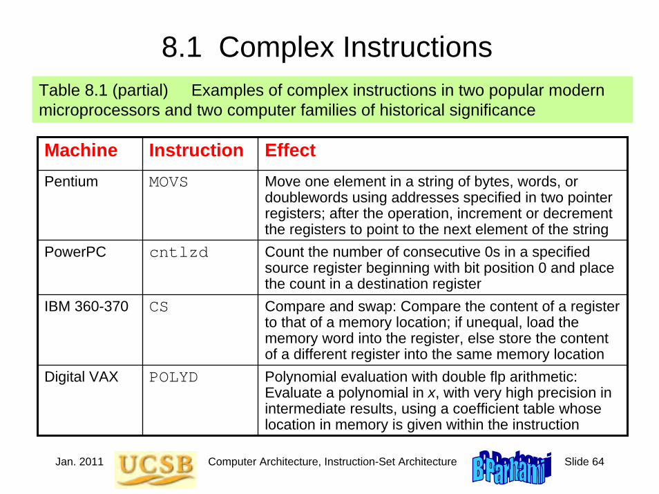
Jan. 2011 Computer Architecture, Instruction-Set Architecture Slide 64
8.1 Complex InstructionsTable 8.1 (partial) Examples of complex instructions in two popular modern microprocessors and two computer families of historical significance
Machine Instruction EffectPentium MOVS Move one element in a string of bytes, words, or
doublewords using addresses specified in two pointer registers; after the operation, increment or decrement the registers to point to the next element of the string
PowerPC cntlzd Count the number of consecutive 0s in a specified source register beginning with bit position 0 and place the count in a destination register
IBM 360-370 CS Compare and swap: Compare the content of a register to that of a memory location; if unequal, load the memory word into the register, else store the content of a different register into the same memory location
Digital VAX POLYD Polynomial evaluation with double flp arithmetic: Evaluate a polynomial in x, with very high precision in intermediate results, using a coefficient table whose location in memory is given within the instruction

Jan. 2011 Computer Architecture, Instruction-Set Architecture Slide 65
Some Details of Sample Complex Instructions
MOVS(Move string)
Sourcestring
Destinationstring
cntlzd(Count leading 0s)
0000 0010 1100 0111
0000 0000 0000 0110
6 leading 0s
POLYD(Polynomial evaluation in
double floating-point)
cn–1xn–1 + . . . + c2x2 + c1x + c0
Coefficients
x

Jan. 2011 Computer Architecture, Instruction-Set Architecture Slide 66
Benefits and Drawbacks of Complex Instructions
Fewer instructions in program(less memory)
Potentially faster execution (complex steps are still done sequentially in multiple cycles, but hardware control can be faster than software loops)
Fewer memory accesses for instructions
Programs may become easier to write/read/understand
More complex format(slower decoding)
Less flexible (one algorithm for polynomial evaluation or sorting may not be the best in all cases)
If interrupts are processed at the end of instruction cycle, machine may become less responsive to time-critical events (interrupt handling)

Jan. 2011 Computer Architecture, Instruction-Set Architecture Slide 67
8.2 Alternative Addressing Modes
Figure 5.11 Schematic representation of addressing modes in MiniMIPS.
Addressing Instruction Other elements involved Operand
Implied
Immediate
Register
Base
PC-relative
Pseudodirect
Some place in the machine
Extend, if required
Reg f ile Reg spec Reg data
Memory Add
Reg file
Mem addr
Constant offset
Reg base Reg data
Mem data
Add
PC
Constant offset
Memory
Mem addr Mem
data
Memory Mem data
PC Mem addr
Let’s refresh our memory (from Chap. 5)
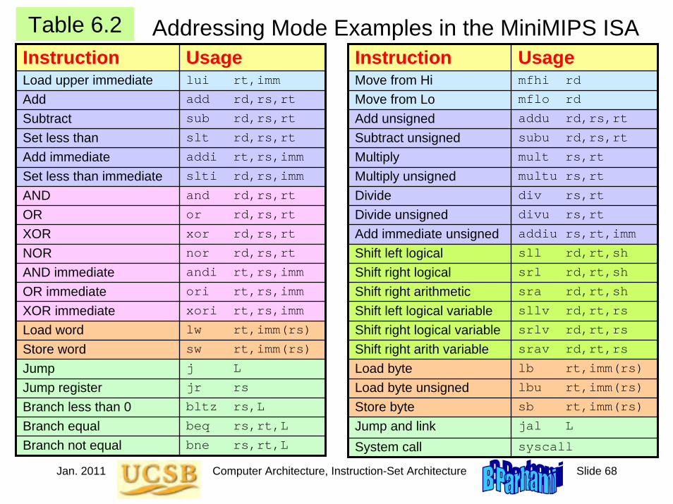
Jan. 2011 Computer Architecture, Instruction-Set Architecture Slide 68
Table 6.2Instruction UsageMove from Hi mfhi rd
Move from Lo mflo rd
Add unsigned addu rd,rs,rt
Subtract unsigned subu rd,rs,rt
Multiply mult rs,rt
Multiply unsigned multu rs,rt
Divide div rs,rt
Divide unsigned divu rs,rt
Add immediate unsigned addiu rs,rt,imm
Shift left logical sll rd,rt,sh
Shift right logical srl rd,rt,sh
Shift right arithmetic sra rd,rt,sh
Shift left logical variable sllv rd,rt,rs
Shift right logical variable srlv rd,rt,rs
Shift right arith variable srav rd,rt,rs
Load byte lb rt,imm(rs)
Load byte unsigned lbu rt,imm(rs)
Store byte sb rt,imm(rs)
Jump and link jal L
System call syscall
Instruction UsageLoad upper immediate lui rt,imm
Add add rd,rs,rt
Subtract sub rd,rs,rt
Set less than slt rd,rs,rt
Add immediate addi rt,rs,imm
Set less than immediate slti rd,rs,imm
AND and rd,rs,rt
OR or rd,rs,rt
XOR xor rd,rs,rt
NOR nor rd,rs,rt
AND immediate andi rt,rs,imm
OR immediate ori rt,rs,imm
XOR immediate xori rt,rs,imm
Load word lw rt,imm(rs)
Store word sw rt,imm(rs)
Jump j L
Jump register jr rs
Branch less than 0 bltz rs,L
Branch equal beq rs,rt,L
Branch not equal bne rs,rt,L
Addressing Mode Examples in the MiniMIPS ISA
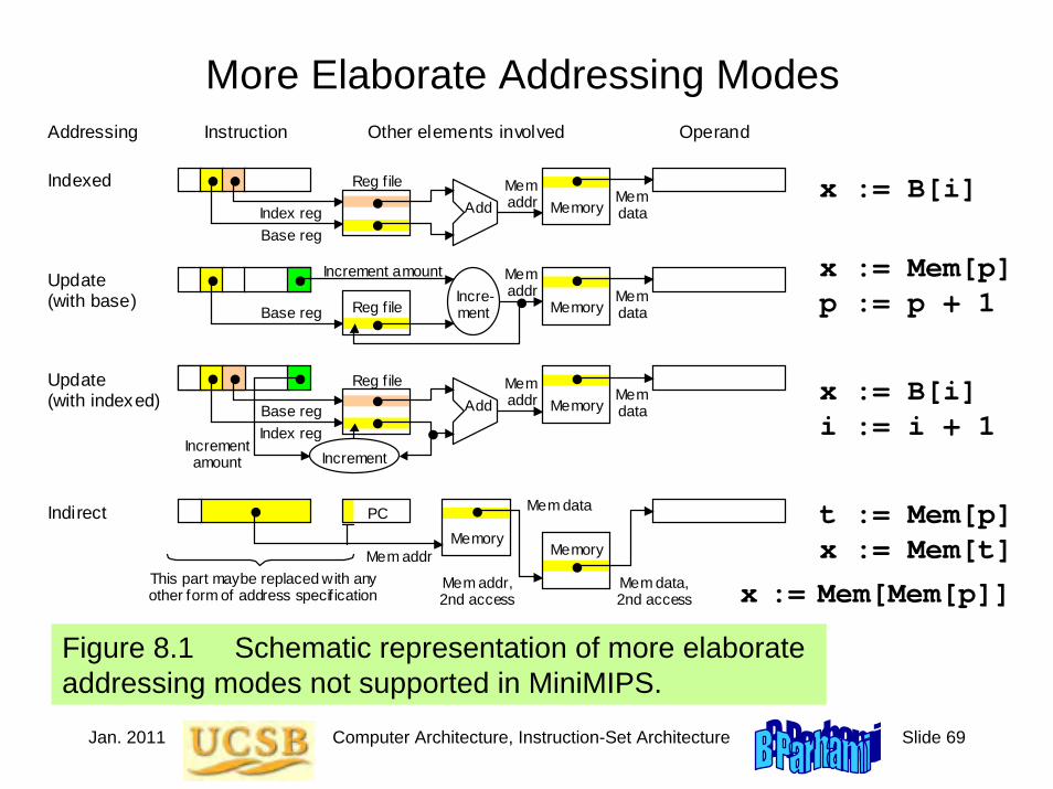
Jan. 2011 Computer Architecture, Instruction-Set Architecture Slide 69
More Elaborate Addressing Modes
Figure 8.1 Schematic representation of more elaborate addressing modes not supported in MiniMIPS.
Addressing Instruction Other elements involved Operand
Mem data PC
Mem addr Memory
Memory Add
Reg f ile Mem addr Mem
data Index reg Base reg
Memory Reg f ile
Mem addr Mem
data
Increment amount
Base reg
Indirect
Indexed
Update (with base)
Update (with indexed) Memory Add
Reg f ile Mem addr Mem
data Index reg Base reg
Increment amount
Memory
Mem addr, 2nd access
Mem data, 2nd access
This part maybe replaced with any other form of address specif ication
Incre-ment
Increment
x := Mem[Mem[p]]
x := B[i]
x := Mem[p]p := p + 1
x := B[i]i := i + 1
t := Mem[p]x := Mem[t]

Jan. 2011 Computer Architecture, Instruction-Set Architecture Slide 70
Usefulness of Some Elaborate Addressing Modes
Update mode: XORing a string of bytes
loop: lb $t0,A($s0)xor $s1,$s1,$t0addi $s0,$s0,-1bne $s0,$zero,loop
One instruction with update addressing
Indirect mode: Case statement
case: lw $t0,0($s0) # get sadd $t0,$t0,$t0 # form 2sadd $t0,$t0,$t0 # form 4sla $t1,T # base Tadd $t1,$t0,$t1lw $t2,0($t1) # entryjr $t2
L0L1L2L3L4L5
TT+4
T+20T+16T+12
T+8
Branch to location Li if s = i (switch var.)

Jan. 2011 Computer Architecture, Instruction-Set Architecture Slide 71
8.3 Variations in Instruction Formats
Figure 8.2 Examples of MiniMIPS instructions with 0 to 3 addresses; shaded fields are unused.
3-address
0-address
1-address
2-address
syscall
j
mult
add
One implied operand in register $v0
Destination and two source registers addressed
Two source registers addressed, destination implied
Jump target addressed (in pseudodirect form)
Category Format Opcode Description of operand(s)
Address 2
12
rt rs 0 24
rt rs 0 rd 32
0
0-, 1-, 2-, and 3-address instructions in MiniMIPS

Jan. 2011 Computer Architecture, Instruction-Set Architecture Slide 72
Zero-Address Architecture: Stack Machine
Stack holds all the operands (replaces our register file)
Load/Store operations become push/pop
Arithmetic/logic operations need only an opcode: they pop operand(s) from the top of the stack and push the result onto the stack
Example: Evaluating the expression (a + b) × (c – d)
a
Push a
ab
Push b
a + b
Add
d
Push d
a + b d
Push c
a + b
c c – d
Subtract
a + bResult
Multiply
If a variable is used again, you may have to push it multiple times
Special instructions such as “Duplicate” and “Swap” are helpful
Polish string: a b + d c – ×

Jan. 2011 Computer Architecture, Instruction-Set Architecture Slide 73
One-Address Architecture: Accumulator Machine
The accumulator, a special register attached to the ALU, always holds operand 1 and the operation result
Only one operand needs to be specified by the instruction
Example: Evaluating the expression (a + b) × (c – d)
May have to store accumulator contents in memory (example above)
No store needed for a + b + c + d + . . . (“accumulator”)
Load aadd bStore tload csubtract dmultiply t
Within branch instructions, the condition or target address must be implied
Branch to L if acc negative
If register x is negative skip the next instruction
Jan. 2011 Computer Architecture, Instruction-Set Architecture Slide 74
Two-Address Architectures
Two addresses may be used in different ways:
Operand1/result and operand 2
Condition to be checked and branch target address
Example: Evaluating the expression (a + b) × (c – d)
A variation is to use one of the addresses as in a one-address machine and the second one to specify a branch in every instruction
load $1,aadd $1,bload $2,csubtract $2,dmultiply $1,$2
Instructions of a hypothetical two-address machine
Jan. 2011 Computer Architecture, Instruction-Set Architecture Slide 75
Components that form a variable-length IA-32 (80x86) instruction.
Example of a Complex Instruction Format
Offset or displacement (0, 1, 2, or 4 B)
Immediate (0, 1, 2, or 4 B)
Opcode (1-2 B)
Instruction prefixes (zero to four, 1 B each)
Mod Reg/Op R/M Scale Index Base
ModR/M SIB
Operand/addresssize overwrites and other modifiers
Most memoryoperands needthese 2 bytes
Instructions can contain up to 15 bytes

Jan. 2011 Computer Architecture, Instruction-Set Architecture Slide 76
Figure 8.3 Example 80x86 instructions ranging in width from 1 to 6 bytes; much wider instructions (up to 15 bytes) also exist
Some of IA-32’s Variable-Width Instructions
4-byte
1-byte
2-byte
3-byte
6-byte
5-byte
Type Format (field widths shown) Opcode Description of operand(s)
8 8 6
PUSH
JE
MOV
XOR
3-bit register specification
8-bit register/mode, 8-bit base/index, 8-bit offset
8-bit register/mode, 8-bit offset
4-bit condition, 8-bit jump offset
ADD
TEST 8-bit register/mode, 32-bit immediate
3-bit register spec, 32-bit immediate
5 3
4 4 8
3 32 4
7 8 32
8 8 8 8

Jan. 2011 Computer Architecture, Instruction-Set Architecture Slide 77
8.4 Instruction Set Design and Evolution
Figure 8.4 Processor design and implementation process.
Pro- cessor design team
New machine project
Tuning & bug fixes
Performance objectives
Instruction-set definition
Imple- men- tation Fabrica-
tion & testing
Sales &
use
?
Feedback
Desirable attributes of an instruction set:
Consistent, with uniform and generally applicable rulesOrthogonal, with independent features noninterferingTransparent, with no visible side effect due to implementation detailsEasy to learn/use (often a byproduct of the three attributes above)Extensible, so as to allow the addition of future capabilitiesEfficient, in terms of both memory needs and hardware realization

Jan. 2011 Computer Architecture, Instruction-Set Architecture Slide 78
8.5 The RISC/CISC DichotomyThe RISC (reduced instruction set computer) philosophy:Complex instruction sets are undesirable because inclusion of mechanisms to interpret all the possible combinations of opcodesand operands might slow down even very simple operations.
Features of RISC architecture
1. Small set of inst’s, each executable in roughly the same time2. Load/store architecture (leading to more registers)3. Limited addressing mode to simplify address calculations4. Simple, uniform instruction formats (ease of decoding)
Ad hoc extension of instruction sets, while maintaining backwardcompatibility, leads to CISC; imagine modern English containingevery English word that has been used through the ages

Jan. 2011 Computer Architecture, Instruction-Set Architecture Slide 79
RISC/CISC Comparison via Generalized Amdahl’s LawExample 8.1
An ISA has two classes of simple (S) and complex (C) instructions. On a reference implementation of the ISA, class-S instructions account for 95% of the running time for programs of interest. A RISC version of the machine is being considered that executes only class-S instructions directly in hardware, with class-C instructions treated as pseudoinstructions. It is estimated that in the RISC version, class-S instructions will run 20% faster while class-C instructions will be slowed down by a factor of 3. Does the RISC approach offer better or worse performance compared to the reference implementation?
SolutionPer assumptions, 0.95 of the work is speeded up by a factor of 1.0 / 0.8 = 1.25, while the remaining 5% is slowed down by a factor of 3. The RISC speedup is 1 / [0.95 / 1.25 + 0.05 × 3] = 1.1. Thus, a 10% improvement in performance can be expected in the RISC version.

Jan. 2011 Computer Architecture, Instruction-Set Architecture Slide 80
Some Hidden Benefits of RISC
In Example 8.1, we established that a speedup factor of 1.1 can be expected from the RISC version of a hypothetical machine
This is not the entire story, however!
If the speedup of 1.1 came with some additional cost, then one might legitimately wonder whether it is worth the expense and design effort
The RISC version of the architecture also:
Reduces the effort and team size for design
Shortens the testing and debugging phase
Simplifies documentation and maintenance
Cheaper product and shorter time-to-market

Jan. 2011 Computer Architecture, Instruction-Set Architecture Slide 81
MIPS Performance Rating RevisitedAn m-MIPS processor can execute m million instructions per second
Comparing an m-MIPS processor with a 10m-MIPS processorLike comparing two people who read m pages and 10m pages per hour
Reading 100 pages per hour, as opposed to 10 pages per hour, maynot allow you to finish the same reading assignment in 1/10 the time
10 pages / hr 100 pages / hr
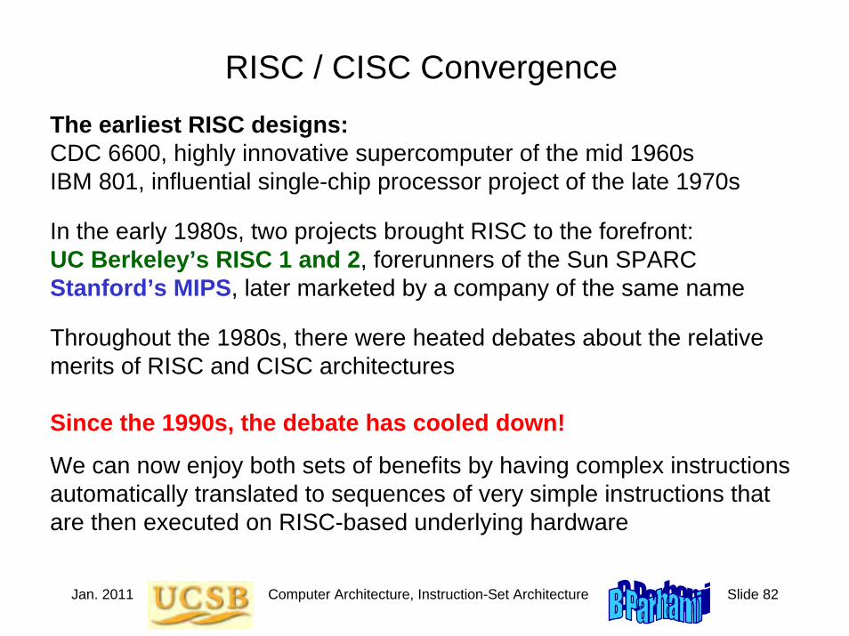
Jan. 2011 Computer Architecture, Instruction-Set Architecture Slide 82
RISC / CISC Convergence
In the early 1980s, two projects brought RISC to the forefront:UC Berkeley’s RISC 1 and 2, forerunners of the Sun SPARCStanford’s MIPS, later marketed by a company of the same name
Since the 1990s, the debate has cooled down!
We can now enjoy both sets of benefits by having complex instructions automatically translated to sequences of very simple instructions that are then executed on RISC-based underlying hardware
The earliest RISC designs:CDC 6600, highly innovative supercomputer of the mid 1960s IBM 801, influential single-chip processor project of the late 1970s
Throughout the 1980s, there were heated debates about the relative merits of RISC and CISC architectures
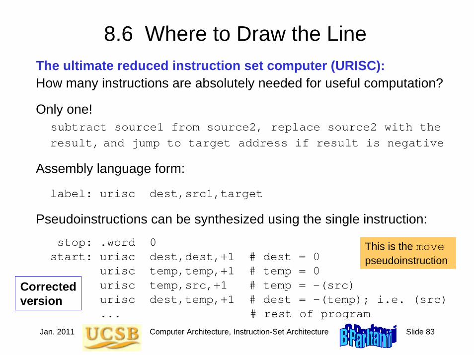
Jan. 2011 Computer Architecture, Instruction-Set Architecture Slide 83
8.6 Where to Draw the LineThe ultimate reduced instruction set computer (URISC):How many instructions are absolutely needed for useful computation?
Only one!subtract source1 from source2, replace source2 with the result, and jump to target address if result is negative
Assembly language form:
label: urisc dest,src1,target
Pseudoinstructions can be synthesized using the single instruction:
stop: .word 0start: urisc dest,dest,+1 # dest = 0
urisc temp,temp,+1 # temp = 0urisc temp,src,+1 # temp = -(src)urisc dest,temp,+1 # dest = -(temp); i.e. (src)... # rest of program
This is the movepseudoinstruction
Correctedversion

Jan. 2011 Computer Architecture, Instruction-Set Architecture Slide 84
Some Useful Pseudo Instructions for URISCExample 8.2 (2 parts of 5)
Write the sequence of instructions that are produced by the URISC assembler for each of the following pseudoinstructions.parta: uadd dest,src1,src2 # dest=(src1)+(src2)partc: uj label # goto label
Solutionat1 and at2 are temporary memory locations for assembler’s use
parta: urisc at1,at1,+1 # at1 = 0urisc at1,src1,+1 # at1 = -(src1)urisc at1,src2,+1 # at1 = -(src1)–(src2)urisc dest,dest,+1 # dest = 0urisc dest,at1,+1 # dest = -(at1)
partc: urisc at1,at1,+1 # at1 = 0urisc at1,one,label # at1 = -1 to force jump

Jan. 2011 Computer Architecture, Instruction-Set Architecture Slide 85
Figure 8.5 Instruction format and hardware structure for URISC.
URISC Hardware
MAR
in
Memory unit
Adder
P C
Write
Read
Word 1
Source 1 Source 2 / Dest Jump target
Word 2 Word 3
URISC instruction:
R M A R
M D R
N Z
PC
in
PC
out
MDR
in
R
in
N in
Z in
C in
Comp
0 1 Mux
0
1
0
R’

Jan. 2011 Computer Architecture, The Arithmetic/Logic Unit Slide 1
Part IIIThe Arithmetic/Logic Unit
Jan. 2011 Computer Architecture, The Arithmetic/Logic Unit Slide 2
About This PresentationThis presentation is intended to support the use of the textbookComputer Architecture: From Microprocessors to Supercomputers, Oxford University Press, 2005, ISBN 0-19-515455-X. It is updated regularly by the author as part of his teaching of the upper-division course ECE 154, Introduction to Computer Architecture, at the University of California, Santa Barbara. Instructors can use these slides freely in classroom teaching and for other educational purposes. Any other use is strictly prohibited. © Behrooz Parhami
Edition Released Revised Revised Revised RevisedFirst July 2003 July 2004 July 2005 Mar. 2006 Jan. 2007
Jan. 2008 Jan. 2009 Jan. 2011
Jan. 2011 Computer Architecture, The Arithmetic/Logic Unit Slide 3
III The Arithmetic/Logic Unit
Topics in This PartChapter 9 Number RepresentationChapter 10 Adders and Simple ALUsChapter 11 Multipliers and DividersChapter 12 Floating-Point Arithmetic
Overview of computer arithmetic and ALU design:• Review representation methods for signed integers• Discuss algorithms & hardware for arithmetic ops• Consider floating-point representation & arithmetic

Jan. 2011 Computer Architecture, The Arithmetic/Logic Unit Slide 4
Preview of Arithmetic Unit in the Data Path
Fig. 13.3 Key elements of the single-cycle MicroMIPS data path.
/
ALU
Data cache
Instr cache
Next addr
Reg file
op
jta
fn
inst
imm
rs (rs)
(rt)
Data addr
Data in 0
1
ALUSrc ALUFunc DataWrite
DataRead
SE
RegInSrc
rt
rd
RegDst RegWrite
32 / 16
Register input
Data out
Func
ALUOvfl
Ovfl
31
0 1 2
Next PC
Incr PC
(PC)
Br&Jump
ALU out
PC
0 1 2
Register writeback
Instruction fetch Reg access / decode ALU operation Data access
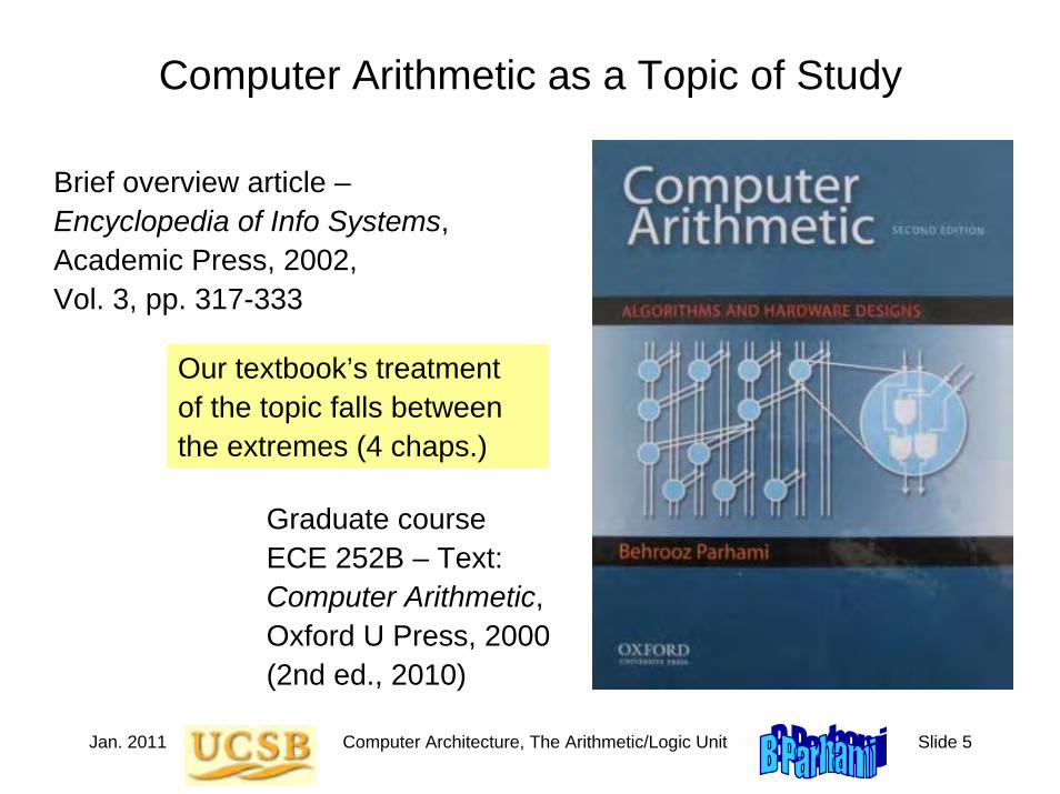
Jan. 2011 Computer Architecture, The Arithmetic/Logic Unit Slide 5
Computer Arithmetic as a Topic of Study
Brief overview article –Encyclopedia of Info Systems,Academic Press, 2002, Vol. 3, pp. 317-333
Our textbook’s treatment of the topic falls between the extremes (4 chaps.)
Graduate courseECE 252B – Text:Computer Arithmetic,Oxford U Press, 2000(2nd ed., 2010)

Jan. 2011 Computer Architecture, The Arithmetic/Logic Unit Slide 6
9 Number RepresentationArguably the most important topic in computer arithmetic:
• Affects system compatibility and ease of arithmetic• Two’s complement, flp, and unconventional methods
Topics in This Chapter9.1 Positional Number Systems9.2 Digit Sets and Encodings9.3 Number-Radix Conversion9.4 Signed Integers9.5 Fixed-Point Numbers9.6 Floating-Point Numbers

Jan. 2011 Computer Architecture, The Arithmetic/Logic Unit Slide 7
9.1 Positional Number Systems
Representations of natural numbers {0, 1, 2, 3, …}||||| ||||| ||||| ||||| ||||| || sticks or unary code
27 radix-10 or decimal code11011 radix-2 or binary codeXXVII Roman numerals
Fixed-radix positional representation with k digits
Value of a number: x = (xk–1xk–2 . . . x1x0)r = Σ xi r i
For example: 27 = (11011)two = (1×24) + (1×23) + (0×22) + (1×21) + (1×20)
Number of digits for [0, P]: k = ⎡logr (P + 1)⎤ = ⎣logr P⎦ + 1
k–1
i=0
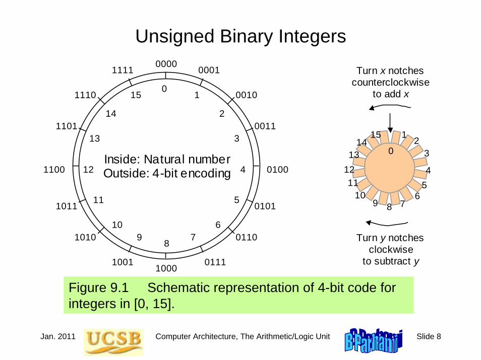
Jan. 2011 Computer Architecture, The Arithmetic/Logic Unit Slide 8
Unsigned Binary Integers
Figure 9.1 Schematic representation of 4-bit code for integers in [0, 15].
0000 0001 1111
0010 1110
0011 1101
0100 1100
1000
0101 1011
0110 1010
0111 1001
0 1
2
3
4
5
6 7
15
11
14
13
12
8 9
10
Inside: Natural number Outside: 4-bit encoding
0
1 2 3
15
4 5
6 7 8 9
Turn x notches counterclockwise
to add x
Turn y notches clockwise
to subtract y
11
14 13
12
10

Jan. 2011 Computer Architecture, The Arithmetic/Logic Unit Slide 9
Representation Range and Overflow
Figure 9.2 Overflow regions in finite number representation systems. For unsigned representations covered in this section, max – = 0.
max
Finite set of representable numbers
Overflow region max Overflow region
Numbers larger than max
Numbers smaller than max
− +
− +
Example 9.2, Part d
Discuss if overflow will occur when computing 317 – 316 in a number system with k = 8 digits in radix r = 10.SolutionThe result 86 093 442 is representable in the number system whichhas a range [0, 99 999 999]; however, if 317 is computed en route to the final result, overflow will occur.

Jan. 2011 Computer Architecture, The Arithmetic/Logic Unit Slide 10
9.2 Digit Sets and Encodings
Conventional and unconventional digit sets
• Decimal digits in [0, 9]; 4-bit BCD, 8-bit ASCII
• Hexadecimal, or hex for short: digits 0-9 & a-f
• Conventional ternary digit set in [0, 2]Conventional digit set for radix r is [0, r – 1]Symmetric ternary digit set in [–1, 1]
• Conventional binary digit set in [0, 1]Redundant digit set [0, 2], encoded in 2 bits( 0 2 1 1 0 )two and ( 1 0 1 0 2 )two represent 22
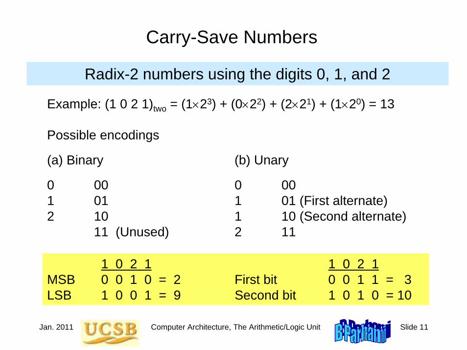
Jan. 2011 Computer Architecture, The Arithmetic/Logic Unit Slide 11
Carry-Save Numbers
Radix-2 numbers using the digits 0, 1, and 2
Example: (1 0 2 1)two = (1×23) + (0×22) + (2×21) + (1×20) = 13
Possible encodings
(a) Binary (b) Unary
0 00 0 001 01 1 01 (First alternate)2 10 1 10 (Second alternate)
11 (Unused) 2 11
1 0 2 1 1 0 2 1MSB 0 0 1 0 = 2 First bit 0 0 1 1 = 3LSB 1 0 0 1 = 9 Second bit 1 0 1 0 = 10

Jan. 2011 Computer Architecture, The Arithmetic/Logic Unit Slide 12
Figure 9.3 Adding a binary number or another carry-save number to a carry-save number.
The Notion of Carry-Save Addition
Two carry-save
inputs
Carry-save input
Binary input
Carry-save output
This bit being 1
represents overflow (ignore it)
0 0
0
a. Carry-save addition. b. Adding two carry-save numbers.
Carry-save addition
Carry-saveaddition
Digit-set combination: {0, 1, 2} + {0, 1} = {0, 1, 2, 3} = {0, 2} + {0, 1}
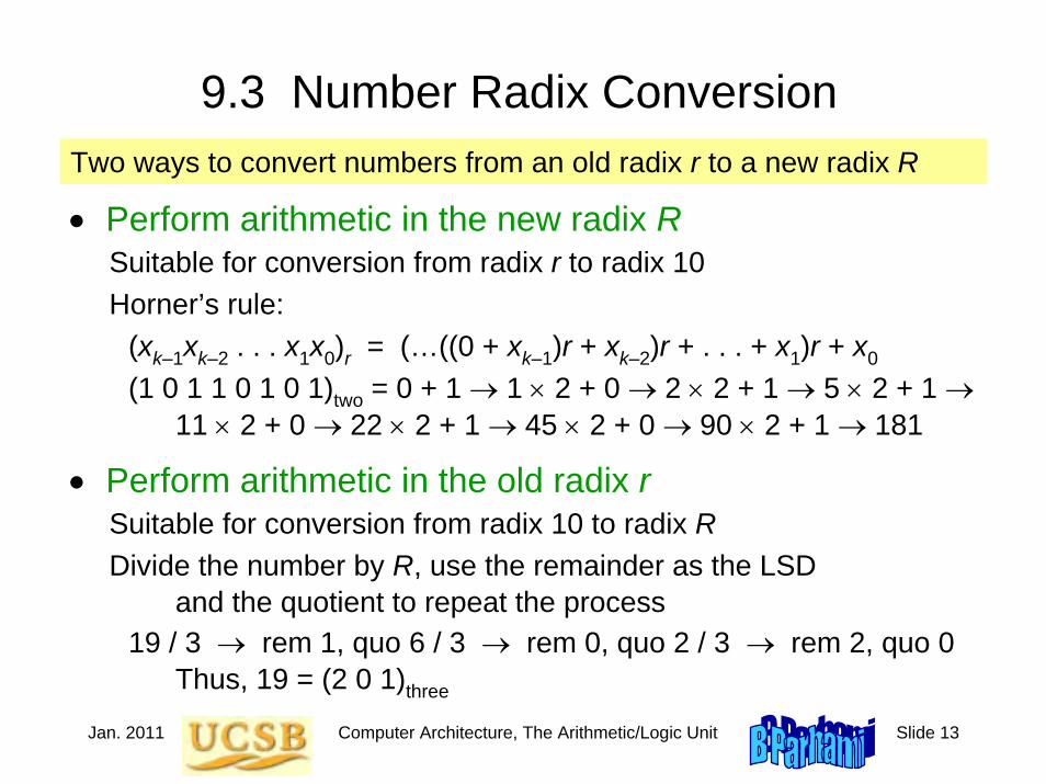
Jan. 2011 Computer Architecture, The Arithmetic/Logic Unit Slide 13
9.3 Number Radix Conversion
• Perform arithmetic in the new radix RSuitable for conversion from radix r to radix 10Horner’s rule:
(xk–1xk–2 . . . x1x0)r = (…((0 + xk–1)r + xk–2)r + . . . + x1)r + x0
(1 0 1 1 0 1 0 1)two = 0 + 1 → 1 × 2 + 0 → 2 × 2 + 1 → 5 × 2 + 1 →11 × 2 + 0 → 22 × 2 + 1 → 45 × 2 + 0 → 90 × 2 + 1 → 181
• Perform arithmetic in the old radix rSuitable for conversion from radix 10 to radix RDivide the number by R, use the remainder as the LSD
and the quotient to repeat the process19 / 3 → rem 1, quo 6 / 3 → rem 0, quo 2 / 3 → rem 2, quo 0
Thus, 19 = (2 0 1)three
Two ways to convert numbers from an old radix r to a new radix R
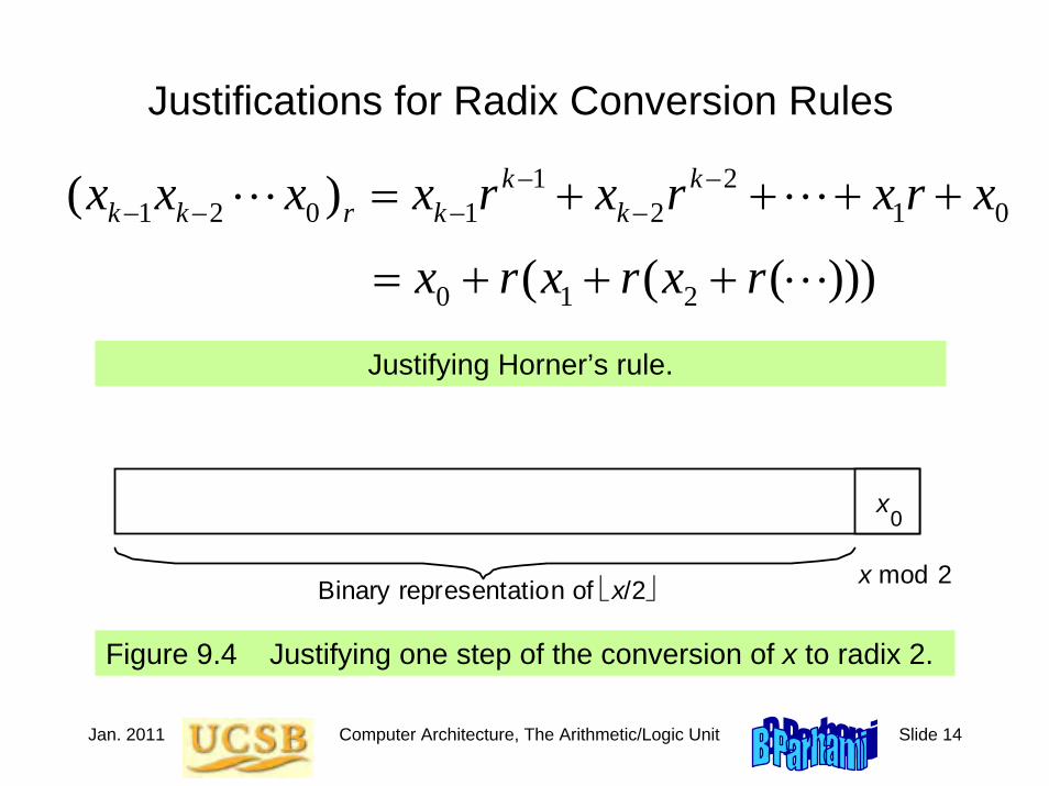
Jan. 2011 Computer Architecture, The Arithmetic/Logic Unit Slide 14
Justifications for Radix Conversion Rules
Figure 9.4 Justifying one step of the conversion of x to radix 2.
x 0
x mod 2 Binary representation of ⎣x/2⎦
Justifying Horner’s rule.
1 21 2 0 1 2 1 0( ) k k
k k r k kx x x x r x r x r x− −− − − −= + + + +L L
0 1 2( ( ( )))x r x r x r= + + + L

Jan. 2011 Computer Architecture, The Arithmetic/Logic Unit Slide 15
9.4 Signed Integers
• We dealt with representing the natural numbers
• Signed or directed whole numbers = integers{ . . . , −3, −2, −1, 0, 1, 2, 3, . . . }
• Signed-magnitude representation+27 in 8-bit signed-magnitude binary code 0 0011011–27 in 8-bit signed-magnitude binary code 1 0011011–27 in 2-digit decimal code with BCD digits 1 0010 0111
• Biased representationRepresent the interval of numbers [−N, P] by the unsigned
interval [0, P + N]; i.e., by adding N to every number
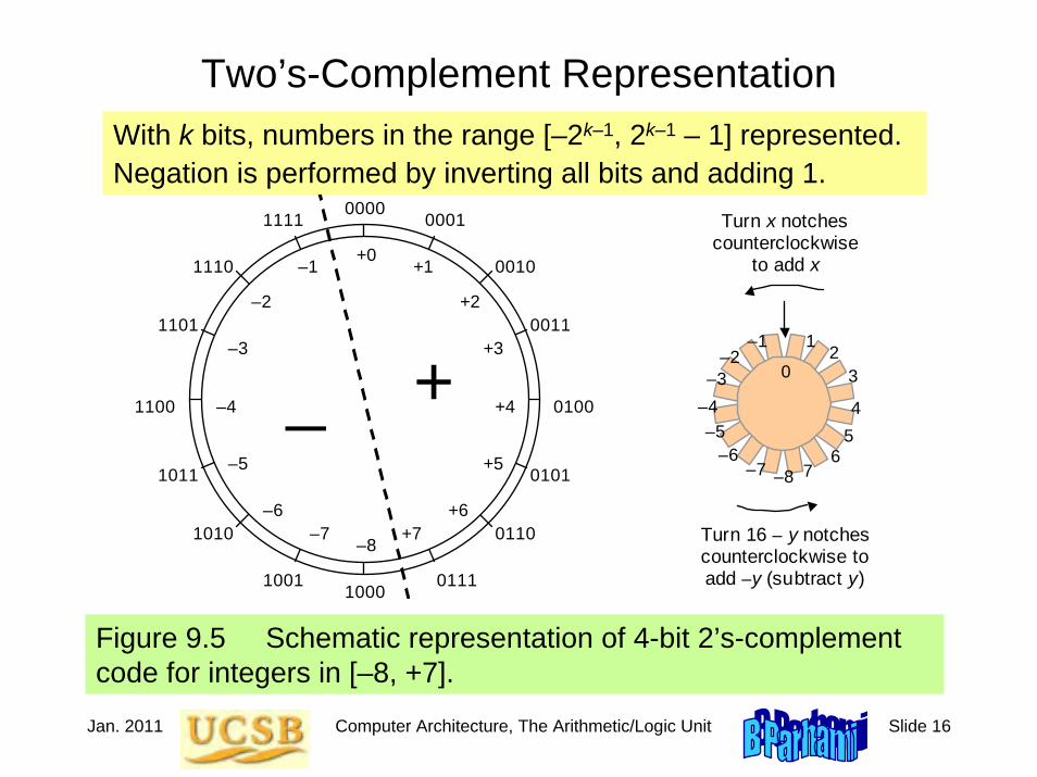
Jan. 2011 Computer Architecture, The Arithmetic/Logic Unit Slide 16
Two’s-Complement Representation
Figure 9.5 Schematic representation of 4-bit 2’s-complement code for integers in [–8, +7].
0000 0001 1111
0010 1110
0011 1101
0100 1100
1000
0101 1011
0110 1010
0111 1001
+0 +1
+2
+3
+4
+5
+6 +7
–1
–5
–2
–3
–4
–8 –7
–6
+ _ 0
1 2
3
–1
4 5
6 7
–8
–7
Turn x notches counterclockwise
to add x
Turn 16 – y notches counterclockwise to add –y (subtract y)
–5
–2 –3
–4
–6
With k bits, numbers in the range [–2k–1, 2k–1 – 1] represented.Negation is performed by inverting all bits and adding 1.

Jan. 2011 Computer Architecture, The Arithmetic/Logic Unit Slide 17
Conversion from 2’s-Complement to DecimalExample 9.7
Convert x = (1 0 1 1 0 1 0 1)2’s-compl to decimal.Solution
Given that x is negative, one could change its sign and evaluate –x.
Shortcut: Use Horner’s rule, but take the MSB as negative–1 × 2 + 0 → –2 × 2 + 1 → –3 × 2 + 1 → –5 × 2 + 0 → –10 × 2 + 1 → –19 × 2 + 0 → –38 × 2 + 1 → –75
Example 9.8Given y = (1 0 1 1 0 1 0 1)2’s-compl, find the representation of –y.Solution
–y = (0 1 0 0 1 0 1 0) + 1 = (0 1 0 0 1 0 1 1)2’s-compl (i.e., 75)
Sign Change for a 2’s-Complement Number

Jan. 2011 Computer Architecture, The Arithmetic/Logic Unit Slide 18
Two’s-Complement Addition and Subtraction
Figure 9.6 Binary adder used as 2’s-complement adder/subtractor.
Add′Sub
x ± y
y
x
k /
k /
k /
y or y ′
Adder
c out
c in
k /

Jan. 2011 Computer Architecture, The Arithmetic/Logic Unit Slide 19
9.5 Fixed-Point NumbersPositional representation: k whole and l fractional digitsValue of a number: x = (xk–1xk–2 . . .x1x0 .x–1x–2 . . . x–l )r = Σ xi r i
For example:
2.375 = (10.011)two = (1×21) + (0×20) + (0×2−1) + (1×2−2) + (1×2−3)
Numbers in the range [0, rk – ulp] representable, where ulp = r –l
Fixed-point arithmetic same as integer arithmetic (radix point implied, not explicit)
Two’s complement properties (including sign change) hold here as well:
(01.011)2’s-compl = (–0×21) + (1×20) + (0×2–1) + (1×2–2) + (1×2–3) = +1.375(11.011)2’s-compl = (–1×21) + (1×20) + (0×2–1) + (1×2–2) + (1×2–3) = –0.625
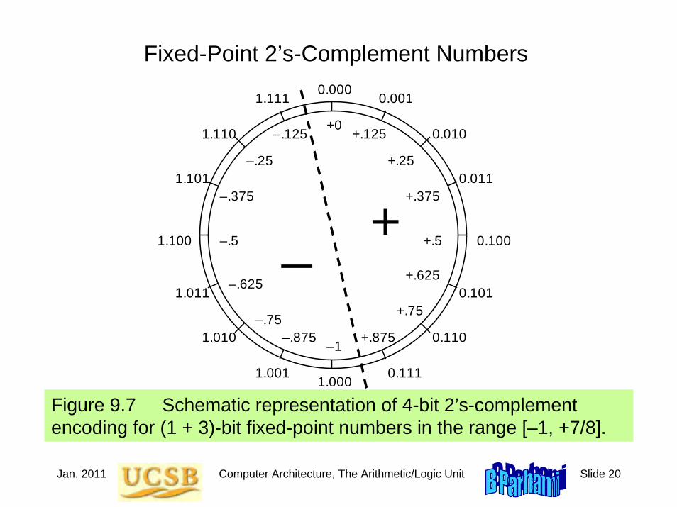
Jan. 2011 Computer Architecture, The Arithmetic/Logic Unit Slide 20
Fixed-Point 2’s-Complement Numbers
Figure 9.7 Schematic representation of 4-bit 2’s-complement encoding for (1 + 3)-bit fixed-point numbers in the range [–1, +7/8].
0.0000.001 1.111
0.010 1.110
0.011 1.101
0.100 1.100
1.000
0.101 1.011
0.110 1.010
0.111 1.001
+0 +.125
+.25
+.375
+.5
+.625
+.75
+.875
–.125
–.625
–.25
–.375
–.5
–1 –.875
–.75
+ _
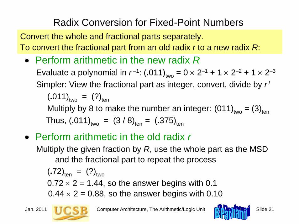
Jan. 2011 Computer Architecture, The Arithmetic/Logic Unit Slide 21
Radix Conversion for Fixed-Point Numbers
• Perform arithmetic in the new radix REvaluate a polynomial in r –1: (.011)two = 0 × 2–1 + 1 × 2–2 + 1 × 2–3
Simpler: View the fractional part as integer, convert, divide by r l
(.011)two = (?)ten
Multiply by 8 to make the number an integer: (011)two = (3)ten
Thus, (.011)two = (3 / 8)ten = (.375)ten
• Perform arithmetic in the old radix rMultiply the given fraction by R, use the whole part as the MSD
and the fractional part to repeat the process(.72)ten = (?)two
0.72 × 2 = 1.44, so the answer begins with 0.10.44 × 2 = 0.88, so the answer begins with 0.10
Convert the whole and fractional parts separately.To convert the fractional part from an old radix r to a new radix R:

Jan. 2011 Computer Architecture, The Arithmetic/Logic Unit Slide 22
9.6 Floating-Point Numbers
• Fixed-point representation must sacrifice precision for small values to represent large values
x = (0000 0000 . 0000 1001)two Small numbery = (1001 0000 . 0000 0000)two Large number
• Neither y2 nor y / x is representable in the format above
• Floating-point representation is like scientific notation: −20 000 000 = −2 × 10⁷ +0.000 000 007 = +7 × 10⁻⁹
Useful for applications where very large and very small numbers are needed simultaneously
Also, 7E−9Significand
ExponentExponent base
Sign

Jan. 2011 Computer Architecture, The Arithmetic/Logic Unit Slide 23
ANSI/IEEE Standard Floating-Point Format (IEEE 754)
Figure 9.8 The two ANSI/IEEE standard floating-point formats.
Short (32-bit) format
Long (64-bit) format
Sign Exponent Significand
8 bits, bias = 127, –126 to 127
11 bits, bias = 1023, –1022 to 1023
52 bits for fractional part (plus hidden 1 in integer part)
23 bits for fractional part (plus hidden 1 in integer part)
Short exponent range is –127 to 128but the two extreme values
are reserved for special operands(similarly for the long format)
Revision (IEEE 754R) was completed in 2008: The revised version includes 16-bit and 128-bit binary formats, as well as 64- and 128-bit decimal formats

Jan. 2011 Computer Architecture, The Arithmetic/Logic Unit Slide 24
Short and Long IEEE 754 Formats: FeaturesTable 9.1 Some features of ANSI/IEEE standard floating-point formats
Feature Single/Short Double/LongWord width in bits 32 64Significand in bits 23 + 1 hidden 52 + 1 hiddenSignificand range [1, 2 – 2–23] [1, 2 – 2–52]Exponent bits 8 11Exponent bias 127 1023Zero (±0) e + bias = 0, f = 0 e + bias = 0, f = 0Denormal e + bias = 0, f ≠ 0
represents ±0.f × 2–126e + bias = 0, f ≠ 0represents ±0.f × 2–1022
Infinity (±∞) e + bias = 255, f = 0 e + bias = 2047, f = 0Not-a-number (NaN) e + bias = 255, f ≠ 0 e + bias = 2047, f ≠ 0Ordinary number e + bias ∈ [1, 254]
e ∈ [–126, 127]represents 1.f × 2e
e + bias ∈ [1, 2046]e ∈ [–1022, 1023]represents 1.f × 2e
min 2–126 ≅ 1.2 × 10–38 2–1022 ≅ 2.2 × 10–308
max ≅ 2128 ≅ 3.4 × 1038 ≅ 21024 ≅ 1.8 × 10308

Jan. 2011 Computer Architecture, The Arithmetic/Logic Unit Slide 25
10 Adders and Simple ALUsAddition is the most important arith operation in computers:
• Even the simplest computers must have an adder• An adder, plus a little extra logic, forms a simple ALU
Topics in This Chapter10.1 Simple Adders
10.2 Carry Propagation Networks
10.3 Counting and Incrementation
10.4 Design of Fast Adders
10.5 Logic and Shift Operations
10.6 Multifunction ALUs

Jan. 2011 Computer Architecture, The Arithmetic/Logic Unit Slide 26
10.1 Simple Adders
Figures 10.1/10.2 Binary half-adder (HA) and full-adder (FA).
x y c s 0 0 0 0 0 1 0 1 1 0 0 1 1 1 1 0
Inputs Outputs
HA
x y
c
s
x y c c s 0 0 0 0 0 0 0 1 0 1 0 1 0 0 1 0 1 1 1 0 1 0 0 0 1 1 0 1 1 0 1 1 0 1 0 1 1 1 1 1
Inputs Outputs
c out c in
out in x
y
s
FA
Digit-set interpretation:{0, 1} + {0, 1}
= {0, 2} + {0, 1}
Digit-set interpretation:{0, 1} + {0, 1} + {0, 1}
= {0, 2} + {0, 1}

Jan. 2011 Computer Architecture, The Arithmetic/Logic Unit Slide 27
Full-Adder Implementations
Figure10.3 Full adder implemented with two half-adders, by means of two 4-input multiplexers, and as two-level gate network.
(a) FA built of two HAs
(c) Two-level AND-OR FA (b) CMOS mux-based FA
1
0
3
2
HA
HA
1
0
3
2
0
1
x y
x y
x y
s
s s
c out
c out
c out
c in
c in
c in

Jan. 2011 Computer Architecture, The Arithmetic/Logic Unit Slide 28
Ripple-Carry Adder: Slow But Simple
Figure 10.4 Ripple-carry binary adder with 32-bit inputs and output.
x
s
y
c c
x
s
y
c
x
s
y
c
c out c in
0 0
0
c 0
1 1
1
1 2
31
31
31
31
FA FA FA 32 . . .
Critical path

Jan. 2011 Computer Architecture, The Arithmetic/Logic Unit Slide 29
Carry Chains and Auxiliary SignalsBit positions
15 14 13 12 11 10 9 8 7 6 5 4 3 2 1 0----------- ----------- ----------- -----------1 0 1 1 0 1 1 0 0 1 1 0 1 1 1 0
cout 0 1 0 1 1 0 0 1 1 1 0 0 0 0 1 1 cin\__________/\__________________/ \________/\____/
4 6 3 2Carry chains and their lengths
g = xy p = x ⊕ y
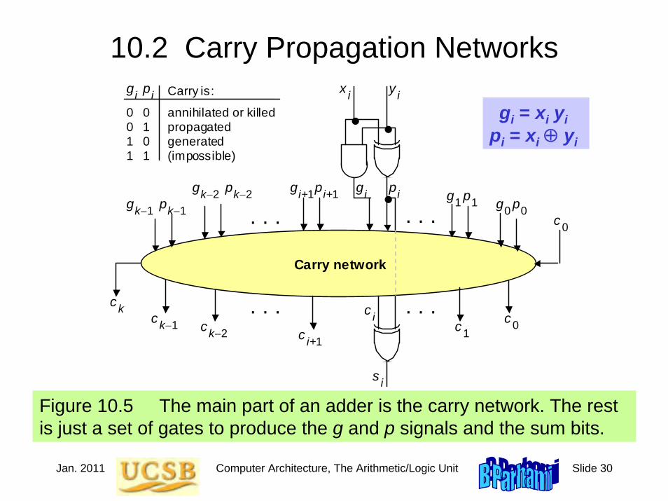
Jan. 2011 Computer Architecture, The Arithmetic/Logic Unit Slide 30
10.2 Carry Propagation Networks
Figure 10.5 The main part of an adder is the carry network. The rest is just a set of gates to produce the g and p signals and the sum bits.
Carry network
. . . . . .
x i y i
g p
s
i i
i
c i c i+1
c k−1
c k c k−2 c 1
c 0
g p 1 1 g p 0 0
g p k−2 k−2 g p i+1 i+1 g p k−1 k−1
c 0 . . . . . .
0 0 0 1 1 0 1 1
annihilated or killed propagated generated (impossible)
Carry is: g i p i gi = xi yi
pi = xi ⊕ yi

Jan. 2011 Computer Architecture, The Arithmetic/Logic Unit Slide 31
Ripple-Carry Adder Revisited
Figure 10.6 The carry propagation network of a ripple-carry adder.
. . . c
k−1
c
k c k−2
c 1
g
p
1
1
g
p
0
0
g
p
k−2
k−2
g
p
k−1
k−1
c
0 c 2
The carry recurrence: ci+1 = gi ∨ pi ci
Latency of k-bit adder is roughly 2k gate delays:
1 gate delay for production of p and g signals, plus 2(k – 1) gate delays for carry propagation, plus1 XOR gate delay for generation of the sum bits

Jan. 2011 Computer Architecture, The Arithmetic/Logic Unit Slide 32
The Complete Design of a Ripple-Carry Adder
Figure 10.6 (ripple-carry network) superimposed on Figure 10.5 (general structure of an adder).
Carry network
. . . . . .
x i y i
g p
s
i i
i
c i c i+1
c k−1
c k c k−2 c 1
c 0
g p 1 1 g p 0 0
g p k−2 k−2 g p i+1 i+1 g p k−1 k−1
c 0 . . . . . .
0 0 0 1 1 0 1 1
annihilated or killed propagated generated (impossible)
Carry is: g i p i gi = xi yi
pi = xi ⊕ yi
. c
1
g
p
1
1
g
p
0
0
c
0 c
2
.c
k−1
c
k c
k−2
g
p
k−2
k−2
g
p
k−1
k−1

Jan. 2011 Computer Architecture, The Arithmetic/Logic Unit Slide 33
First Carry Speed-Up Method: Carry Skip
Figures 10.7/10.8 A 4-bit section of a ripple-carry network with skip paths and the driving analogy.
c
g
p
4j+1
4j+1
g
p
4j
4j
g
p
4j+2
4j+2
g
p
4j+3
4j+3
c
4j
4j+4
c
4j+3
c
4j+2
c
4j+1
One-way street
Freeway

Jan. 2011 Computer Architecture, The Arithmetic/Logic Unit Slide 34
Mux-Based Skip Carry Logic
The carry-skip adder of Fig. 10.7 works fine if we begin with a clean slate, where all signals are 0s; otherwise, it will run into problems, which do not exist in this mux-based implementation
c
g
p
4j+1
4j+1
g
p
4j
4j
g
p
4j+2
4j+2
g
p
4j+3
4j+3
c
4j
4j+4
c
4j+3
c
4j+2
c
4j+1
01
p[4j, 4j+3]
c4j+4
c
g
p
4j+1
4j+1
g
p
4j
4j
g
p
4j+2
4j+2
g
p
4j+3
4j+3
c
4j
4j+4
c
4j+3
c
4j+2
c
4j+1
Fig. 10.7

Jan. 2011 Computer Architecture, The Arithmetic/Logic Unit Slide 35
10.3 Counting and Incrementation
Figure 10.9 Schematic diagram of an initializable synchronous counter.
D Q
C _ Q
D
c out
c in
Adder
Update
/ k
k /
a (Increment
amount)
Count register k
/ 1
0
Data in
k /
k /
Incr′Init

Jan. 2011 Computer Architecture, The Arithmetic/Logic Unit Slide 36
Circuit for Incrementation by 1
Substantially simpler than an adder
Figure 10.10 Carry propagation network and sum logic for an incrementer.
1
0
k−2
k−1
. . . c
k−1
c
k
c
k−2
c
1
x
x
x
x
c
2
1 0 k−2 k−1 s s s s 2 s
. . . c k−1
c
k c k−2
c 1
g
p
1
1
g
p
0
0
g
p
k−2
k−2
g
p
k−1
k−1
c
0 c
2
00x0x1
Figure 10.6
1

Jan. 2011 Computer Architecture, The Arithmetic/Logic Unit Slide 37
• Carries can be computed directly without propagation• For example, by unrolling the equation for c3, we get:
c3 = g2 ∨ p2 c2 = g2 ∨ p2 g1 ∨ p2 p1 g0 ∨ p2 p1 p0 c0
• We define “generate” and “propagate” signals for a block extending from bit position a to bit position b as follows:
g[a,b] = gb ∨ pb gb–1 ∨ pb pb–1gb–2 ∨ . . . ∨ pb pb–1…pa+1 ga
p[a,b] = pb pb–1 . . . pa+1 pa
• Combining g and p signals for adjacent blocks:g[h,j] = g[i+1,j] ∨ p[i+1,j] g[h,i]
p[h,j] = p[i+1,j] p[h,i]
10.4 Design of Fast Adders
hii+1j
[h, j] = [i + 1, j] ¢ [h, i]

Jan. 2011 Computer Architecture, The Arithmetic/Logic Unit Slide 38
Carries as Generate Signals for Blocks [ 0, i ]
Figure 10.5
Carry network
. . . . . .
x i y i
g p
s
i i
i
c i c i+1
c k−1
c k c k−2 c 1
c 0
g p 1 1 g p 0 0
g p k−2 k−2 g p i+1 i+1 g p k−1 k−1
c 0 . . . . . .
0 0 0 1 1 0 1 1
annihilated or killed propagated generated (impossible)
Carry is: g i p i
Assuming c0 = 0, we have ci = g [0,i –1]

Jan. 2011 Computer Architecture, The Arithmetic/Logic Unit Slide 39
Second Carry Speed-Up Method: Carry Lookahead
Figure 10.11 Brent-Kung lookahead carry network for an 8-digit adder, along with details of one of the carry operator blocks.
¢ ¢ ¢ ¢
¢ ¢
¢ ¢
¢ ¢ ¢
[7, 7 ] [6, 6 ] [5, 5 ] [4, 4 ] [3, 3 ] [2, 2 ] [1, 1 ] [0, 0 ]
[0, 7 ] [0, 6 ] [0, 5 ] [0, 4 ] [0, 3 ] [0, 2 ] [0, 1 ] [0, 0 ]
[2, 3 ] [4, 5 ]
[6, 7 ]
[4, 7 ] [0, 3 ]
[0, 1 ]
g [0, 0]
g [0, 1]
g [1, 1]
p [0, 0]
p [0, 1]
p [1, 1]
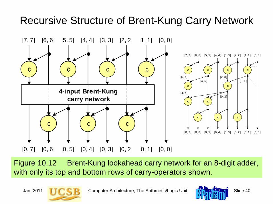
Jan. 2011 Computer Architecture, The Arithmetic/Logic Unit Slide 40
Recursive Structure of Brent-Kung Carry Network
Figure 10.12 Brent-Kung lookahead carry network for an 8-digit adder, with only its top and bottom rows of carry-operators shown.
¢ ¢ ¢ ¢
¢ ¢ ¢
[7, 7] [6, 6] [5, 5] [4, 4] [3, 3] [2, 2] [1, 1] [0, 0]
[0, 7] [0, 6] [0, 5] [0, 4] [0, 3] [0, 2] [0, 1] [0, 0]
4-input Brent-Kung carry network
¢ ¢ ¢ ¢
¢ ¢
¢ ¢
¢ ¢ ¢
[7, 7 ] [6, 6 ] [5, 5 ] [4, 4 ] [3, 3 ] [2, 2 ] [1, 1 ] [0, 0 ]
[0, 7 ] [0, 6 ] [0, 5 ] [0, 4 ] [0, 3 ] [0, 2 ] [0, 1 ] [0, 0 ]
[2, 3 ] [4, 5 ]
[6, 7 ]
[4, 7 ] [0, 3 ]
[0, 1 ]

Jan. 2011 Computer Architecture, The Arithmetic/Logic Unit Slide 41
An Alternate Design: Kogge-Stone Network
Kogge-Stone lookahead carry network for an 8-digit adder.
¢ ¢ ¢ ¢
¢ ¢ ¢ ¢
¢ ¢
¢ ¢¢ ¢
¢
¢ ¢
c1 = g [0,0]c2 = g [0,1]
c3 = g [0,2]c8 = g [0,7] c4 = g [0,3]
c5 = g [0,4]c6 = g [0,5]
c7 = g [0,6]

Jan. 2011 Computer Architecture, The Arithmetic/Logic Unit Slide 42
¢ ¢ ¢ ¢
¢ ¢
¢ ¢
¢ ¢ ¢
[7, 7 ] [6, 6 ] [5, 5 ] [4, 4 ] [3, 3 ] [2, 2 ] [1, 1 ] [0, 0 ]
[0, 7 ] [0, 6 ] [0, 5 ] [0, 4 ] [0, 3 ] [0, 2 ] [0, 1 ] [0, 0 ]
[2, 3 ] [4, 5 ]
[6, 7 ]
[4, 7 ] [0, 3 ]
[0, 1 ]
g [0, 0]
g [0, 1]
g [1, 1]
p [0, 0]
p [0, 1]
p [1, 1]
Brent-Kung vs. Kogge-Stone Carry Network
11 carry operators4 levels
17 carry operators3 levels

Jan. 2011 Computer Architecture, The Arithmetic/Logic Unit Slide 43
Carry-Lookahead Logic with 4-Bit Block
Figure 10.13 Blocks needed in the design of carry-lookahead adders with four-way grouping of bits.
Bloc
k si
gnal
gen
erat
ion
p [i, i+3]
c i
Inte
rmei
dte
carr
ies
c i+1 c i+2 c i+3 g [i, i+3]
p i+3 g i+3 p i+2 g i+2 p i+1 g i+1 p i g i

Jan. 2011 Computer Architecture, The Arithmetic/Logic Unit Slide 44
Third Carry Speed-Up Method: Carry Select
Figure 10.14 Carry-select addition principle.
c out c in Adder
Version 1 of sum bits 1
0
x [a, b]
c out c in Adder
Version 0 of sum bits
y [a, b]
s [a, b]
c a
0 1
Allows doubling of adder width with a single-mux additional delay
The lowera positions, (0 to a – 1) are added as usual

Jan. 2011 Computer Architecture, The Arithmetic/Logic Unit Slide 45
10.5 Logic and Shift OperationsConceptually, shifts can be implemented by multiplexing
Figure 10.15 Multiplexer-based logical shifting unit.
Multiplexer
0 1 2 31 32 33 62 63
5
6
Right’Left Shift amount 0, x[31, 1]
x[31, 0]
00, x[30, 2] 00...0, x[31]
x[31, 0] x[30, 0], 0
x[1, 0], 00...0 x[0], 00...0
. . . . . .
32
32 32 32 32 32 32 32 32
6-bit code specifying shift direction & amount
Right-shifted values
Left-shifted values
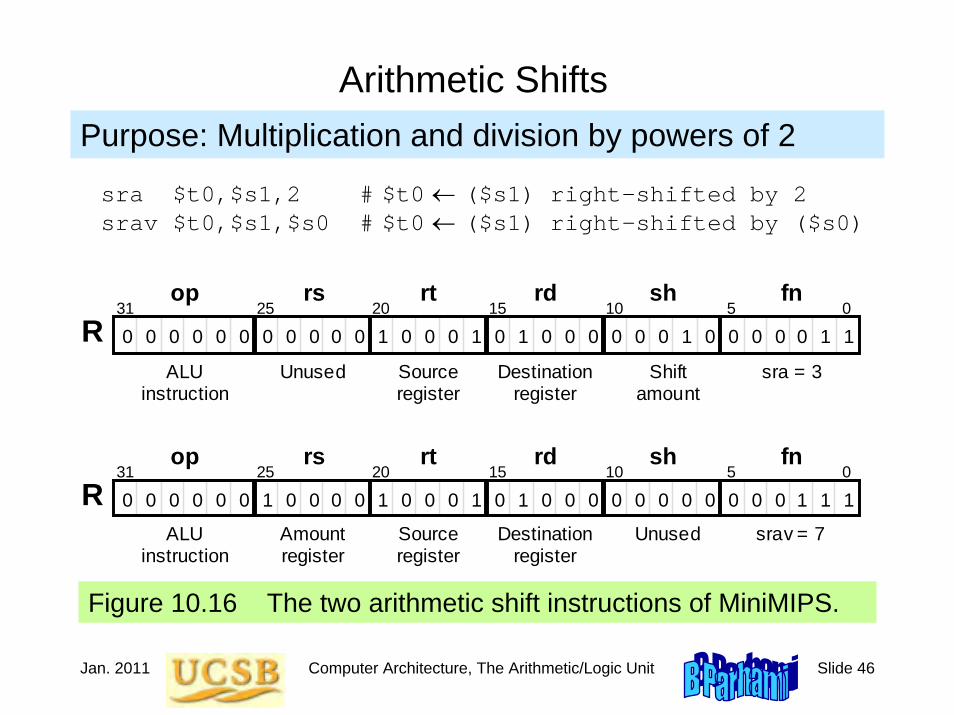
Jan. 2011 Computer Architecture, The Arithmetic/Logic Unit Slide 46
Arithmetic Shifts
Figure 10.16 The two arithmetic shift instructions of MiniMIPS.
Purpose: Multiplication and division by powers of 2
sra $t0,$s1,2 # $t0 ← ($s1) right-shifted by 2srav $t0,$s1,$s0 # $t0 ← ($s1) right-shifted by ($s0)
1 1
1 1
0 0 0
fn
0 0 0 0 0 0 0 0 0 0 0 1 0 0 0 0 1 1 1 0 0 0 0 0 0 0 0 31 25 20 15 0
ALU instruction
Unused Source register
op rs rt
R rd sh
10 5
Destination register
Shift amount
sra = 3
1 0 0 0 0 0 0 0 0 0 0 0 0 0 0 0 0 0 1 1 1 1 0 0 0 0 0 0 0 0 31 25 20 15 0
ALU instruction
Amount register
Source register
op rs rt
R rd sh
10 5 fn
Destination register
Unused srav = 7

Jan. 2011 Computer Architecture, The Arithmetic/Logic Unit Slide 47
Practical Shifting in Multiple Stages
Figure 10.17 Multistage shifting in a barrel shifter.
2
0, x[31, 1]
x[31, 0] x[30, 0], 0
32
0 1 2 3
32 32 32 32
0 0 No shift 0 1 Logical left 1 0 Logical right 1 1 Arith right
x[31], x[31, 1]
Multiplexer
2
0 1 2 3 (0 or 4)-bit shift
2
0 1 2 3 (0 or 2)-bit shift
2
0 1 2 3 (0 or 1)-bit shift
(a) Single-bit shifter (b) Shifting by up to 7 bits
y[31, 0]
z[31, 0]

Jan. 2011 Computer Architecture, The Arithmetic/Logic Unit Slide 48
Figure 10.18 A 4 × 8 block of a black-and-white image represented as a 32-bit word.
32-pixel (4 × 8) block of black-and-white image:
Bit Manipulation via Shifts and Logical Operations
AND with mask to isolate a field: 0000 0000 0000 0000 1111 1100 0000 0000
Right-shift by 10 positions to move field to the right end of word
The result word ranges from 0 to 63, depending on the field pattern
1010 0000 0101 1000 0000 0110 0001 0111 Representation as 32-bit word:
Hex equivalent: 0xa0a80617
Row 0 Row 1 Row 2 Row 3
Bits 10-15

Jan. 2011 Computer Architecture, The Arithmetic/Logic Unit Slide 49
10.6 Multifunction ALUs
General structure of a simple arithmetic/logic unit.
Logicunit
Arithunit 0
1
Arith fn (add, sub, . . .)
Select fn type (logic or arith)
Operand 1
Operand 2
Result
Logic fn (AND, OR, . . .)
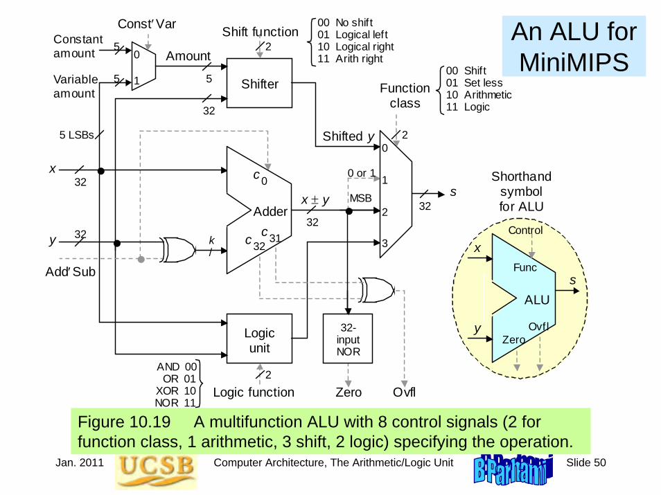
Jan. 2011 Computer Architecture, The Arithmetic/Logic Unit Slide 50
An ALU for MiniMIPS
Figure 10.19 A multifunction ALU with 8 control signals (2 for function class, 1 arithmetic, 3 shift, 2 logic) specifying the operation.
Add′Sub
x ± y
y
x
Adder
c 32
c 0
k /
Shifter
Logic unit
s
Logic function
Amount
5
2
Constant amount
Variable amount
5
5
Const′Var
0
1
0
1
2
3
Function class
2
Shift function
5 LSBs Shifted y
32
32
32
2
c 31
32-input NOR
Ovfl Zero
32 32
MSB
ALU
y
x
s
Shorthand symbol for ALU
Ovfl Zero
Func
Control
0 or 1
AND 00 OR 01
XOR 10 NOR 11
00 Shift 01 Set less 10 Arithmetic 11 Logic
00 No shift 01 Logical left 10 Logical right 11 Arith right

Jan. 2011 Computer Architecture, The Arithmetic/Logic Unit Slide 51
11 Multipliers and DividersModern processors perform many multiplications & divisions:
• Encryption, image compression, graphic rendering• Hardware vs programmed shift-add/sub algorithms
Topics in This Chapter
11.1 Shift-Add Multiplication
11.2 Hardware Multipliers
11.3 Programmed Multiplication
11.4 Shift-Subtract Division
11.5 Hardware Dividers
11.6 Programmed Division

Jan. 2011 Computer Architecture, The Arithmetic/Logic Unit Slide 52
11.1 Shift-Add Multiplication
Figure 11.1 Multiplication of 4-bit numbers in dot notation.
Multiplicand
Partial products bit-matrix
x y
z
y x 2 0 0
y x 2 1 1
y x 2 2 2
y x 2 3 3
Multiplier
Product
z(j+1) = (z(j) + yj x 2k) 2–1 with z(0) = 0 and z(k) = z|––– add –––||–– shift right ––|

Jan. 2011 Computer Architecture, The Arithmetic/Logic Unit Slide 53
Binary and Decimal Multiplication
Figure 11.2 Step-by-step multiplication examples for 4-digit unsigned numbers.
Position 7 6 5 4 3 2 1 0 Position 7 6 5 4 3 2 1 0========================= =========================x24 1 0 1 0 x104 3 5 2 8y 0 0 1 1 y 4 0 6 7========================= =========================z (0) 0 0 0 0 z (0) 0 0 0 0+y0x24 1 0 1 0 +y0x104 2 4 6 9 6–––––––––––––––––––––––––– ––––––––––––––––––––––––––2z (1) 0 1 0 1 0 10z (1) 2 4 6 9 6z (1) 0 1 0 1 0 z (1) 0 2 4 6 9 6+y1x24 1 0 1 0 +y1x104 2 1 1 6 8–––––––––––––––––––––––––– ––––––––––––––––––––––––––2z (2) 0 1 1 1 1 0 10z (2) 2 3 6 3 7 6z (2) 0 1 1 1 1 0 z (2) 2 3 6 3 7 6+y2x24 0 0 0 0 +y2x104 0 0 0 0 0–––––––––––––––––––––––––– ––––––––––––––––––––––––––2z (3) 0 0 1 1 1 1 0 10z (3) 0 2 3 6 3 7 6z (3) 0 0 1 1 1 1 0 z (3) 0 2 3 6 3 7 6+y3x24 0 0 0 0 +y3x104 1 4 1 1 2–––––––––––––––––––––––––– ––––––––––––––––––––––––––2z (4) 0 0 0 1 1 1 1 0 10z (4) 1 4 3 4 8 3 7 6z (4) 0 0 0 1 1 1 1 0 z (4) 1 4 3 4 8 3 7 6========================= =========================
Example 11.1
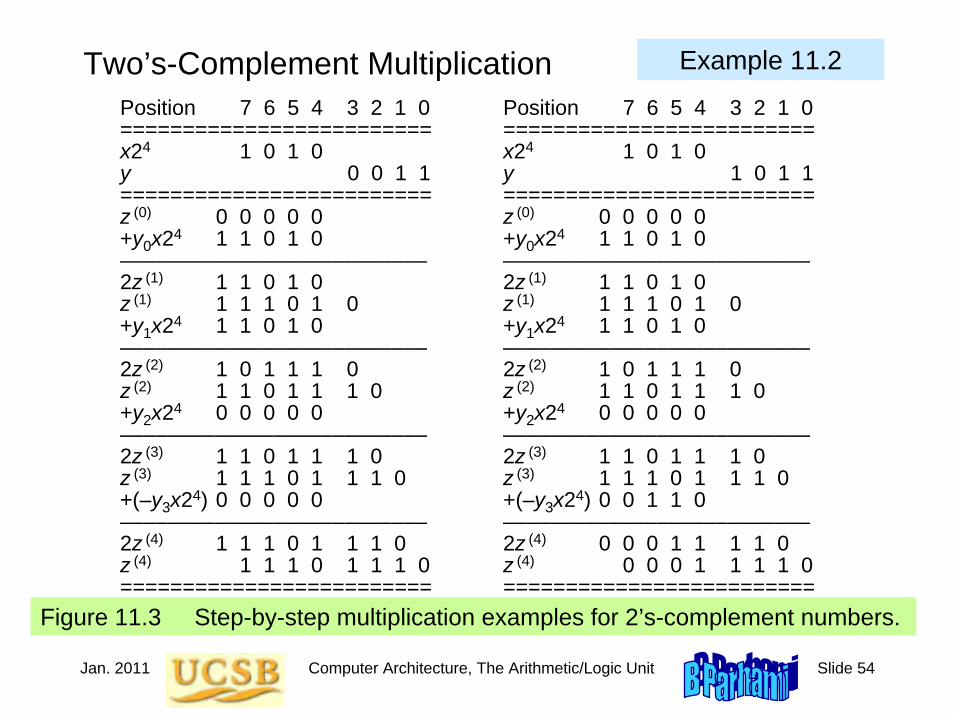
Jan. 2011 Computer Architecture, The Arithmetic/Logic Unit Slide 54
Two’s-Complement Multiplication
Figure 11.3 Step-by-step multiplication examples for 2’s-complement numbers.
Position 7 6 5 4 3 2 1 0 Position 7 6 5 4 3 2 1 0========================= =========================x24 1 0 1 0 x24 1 0 1 0y 0 0 1 1 y 1 0 1 1========================= =========================z (0) 0 0 0 0 0 z (0) 0 0 0 0 0+y0x24 1 1 0 1 0 +y0x24 1 1 0 1 0–––––––––––––––––––––––––– ––––––––––––––––––––––––––2z (1) 1 1 0 1 0 2z (1) 1 1 0 1 0z (1) 1 1 1 0 1 0 z (1) 1 1 1 0 1 0+y1x24 1 1 0 1 0 +y1x24 1 1 0 1 0–––––––––––––––––––––––––– ––––––––––––––––––––––––––2z (2) 1 0 1 1 1 0 2z (2) 1 0 1 1 1 0z (2) 1 1 0 1 1 1 0 z (2) 1 1 0 1 1 1 0+y2x24 0 0 0 0 0 +y2x24 0 0 0 0 0–––––––––––––––––––––––––– ––––––––––––––––––––––––––2z (3) 1 1 0 1 1 1 0 2z (3) 1 1 0 1 1 1 0z (3) 1 1 1 0 1 1 1 0 z (3) 1 1 1 0 1 1 1 0+(–y3x24) 0 0 0 0 0 +(–y3x24) 0 0 1 1 0–––––––––––––––––––––––––– ––––––––––––––––––––––––––2z (4) 1 1 1 0 1 1 1 0 2z (4) 0 0 0 1 1 1 1 0z (4) 1 1 1 0 1 1 1 0 z (4) 0 0 0 1 1 1 1 0========================= =========================
Example 11.2
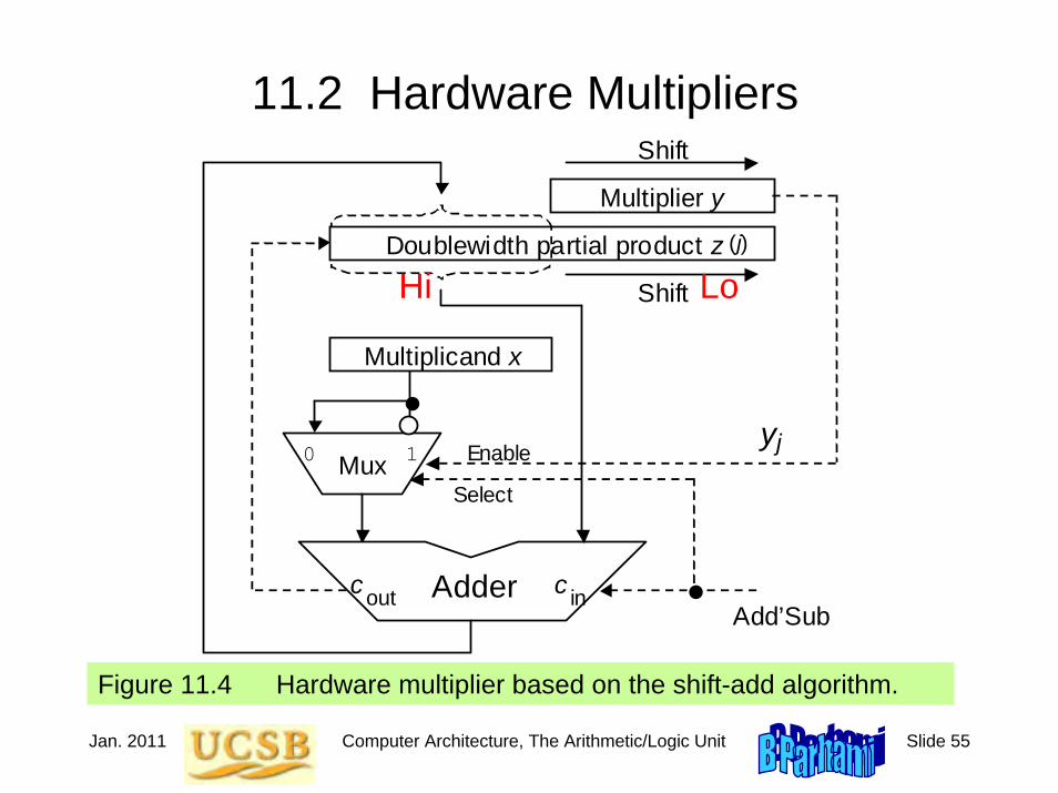
Jan. 2011 Computer Architecture, The Arithmetic/Logic Unit Slide 55
11.2 Hardware Multipliers
Multiplier y
Mux
Adder out c
0 1
Doublewidth partial product z
Multiplicand x
Shift
Shift
(j)
j y
Add’Sub
Enable
Select
in c
Figure 11.4 Hardware multiplier based on the shift-add algorithm.
Hi Lo

Jan. 2011 Computer Architecture, The Arithmetic/Logic Unit Slide 56
The Shift Part of Shift-Add
Figure11.5 Shifting incorporated in the connections to the partial product register rather than as a separate phase.
out c
To adder j y
From adderSum
Partial product Multiplier
/ k – 1
/ k – 1
/ k
/ k

Jan. 2011 Computer Architecture, The Arithmetic/Logic Unit Slide 57
High-Radix Multipliers
Radix-4 multiplication in dot notation.
Multiplicand x y
z
Multiplier
Product
0, x, 2x, or 3x
z(j+1) = (z(j) + yj x 2k) 4–1 with z(0) = 0 and z(k/2) = z|––– add –––||–– shift right ––| Assume k even

Jan. 2011 Computer Architecture, The Arithmetic/Logic Unit Slide 58
Tree Multipliers
Figure 11.6 Schematic diagram for full/partial-tree multipliers.
Adder
Large tree of carry-save
adders
. . .
All partial products
Product
Adder
Small tree of carry-save
adders
. . .
Several partial products
Product
Log-depth
Log-depth
(a) Full-tree multiplier (b) Partial-tree multiplier
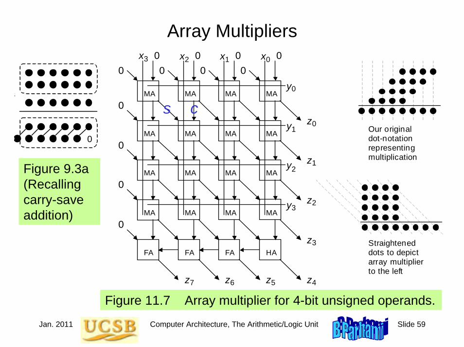
Jan. 2011 Computer Architecture, The Arithmetic/Logic Unit Slide 59
Array Multipliers
Figure 11.7 Array multiplier for 4-bit unsigned operands.
3
2
1
0
4 5 6 7
0
1
2
3
2 1 0 x x x
y
y
y
z
y
3 x
0 0
0 0
0 0
0 0
0
0
0 z
z
z
z z z z
HA FA FA
MA MA MA MA
MA MA MA MA
MA MA MA MA
MA MA MA MA
FA
0
Our original dot-notation representing multiplication
Straightened dots to depict array multiplier to the left
s cs
0
Figure 9.3a (Recalling carry-save addition)
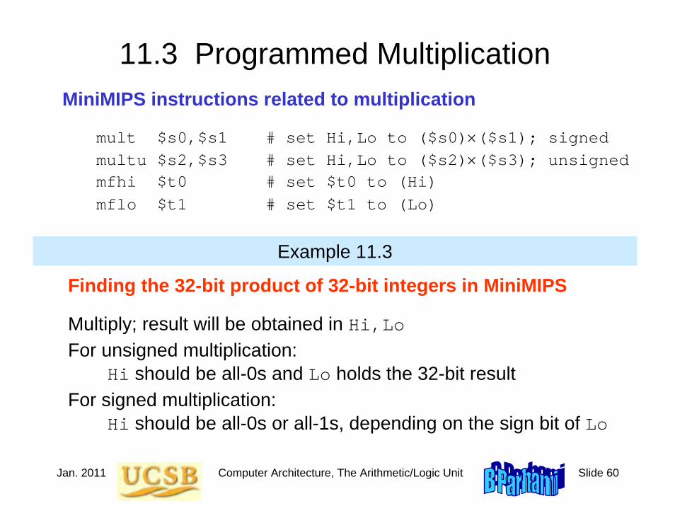
Jan. 2011 Computer Architecture, The Arithmetic/Logic Unit Slide 60
11.3 Programmed MultiplicationMiniMIPS instructions related to multiplication
mult $s0,$s1 # set Hi,Lo to ($s0)×($s1); signedmultu $s2,$s3 # set Hi,Lo to ($s2)×($s3); unsignedmfhi $t0 # set $t0 to (Hi)mflo $t1 # set $t1 to (Lo)
Finding the 32-bit product of 32-bit integers in MiniMIPS
Multiply; result will be obtained in Hi,LoFor unsigned multiplication:
Hi should be all-0s and Lo holds the 32-bit resultFor signed multiplication:
Hi should be all-0s or all-1s, depending on the sign bit of Lo
Example 11.3

Jan. 2011 Computer Architecture, The Arithmetic/Logic Unit Slide 61
Figure 11.8 Register usage for programmed multiplication superimposed on the block diagram for a hardware multiplier.
Emulating a Hardware Multiplier in Software
$t2 (counter) Part of thecontrol in hardware
Also, holdsLSB of Hi during shift
Multiplier y
Mux
Adder out
c
0 1
Doublewidth partial product z
Multiplicand x
Shift
Shift
(j)
j
y
Add’Sub
Enable
Select
in
c
$a0 (multiplicand x)
$a1 (multiplier y)
$v1 (Lo part of z) $v0 (Hi part of z)
$t0 (carry-out)
$t1 (bit j of y)
Example 11.4 (MiniMIPS shift-add program for multiplication)

Jan. 2011 Computer Architecture, The Arithmetic/Logic Unit Slide 62
shamu: move $v0,$zero # initialize Hi to 0move $vl,$zero # initialize Lo to 0addi $t2,$zero,32 # init repetition counter to 32
mloop: move $t0,$zero # set c-out to 0 in case of no addmove $t1,$a1 # copy ($a1) into $t1srl $a1,1 # halve the unsigned value in $a1subu $t1,$t1,$a1 # subtract ($a1) from ($t1) twice tosubu $t1,$t1,$a1 # obtain LSB of ($a1), or y[j], in $t1beqz $t1,noadd # no addition needed if y[j] = 0addu $v0,$v0,$a0 # add x to upper part of zsltu $t0,$v0,$a0 # form carry-out of addition in $t0
noadd: move $t1,$v0 # copy ($v0) into $t1srl $v0,1 # halve the unsigned value in $v0subu $t1,$t1,$v0 # subtract ($v0) from ($t1) twice tosubu $t1,$t1,$v0 # obtain LSB of Hi in $t1sll $t0,$t0,31 # carry-out converted to 1 in
MSB of $t0addu $v0,$v0,$t0 # right-shifted $v0 correctedsrl $v1,1 # halve the unsigned value in $v1sll $t1,$t1,31 # LSB of Hi converted to 1 in
MSB of $t1addu $v1,$v1,$t1 # right-shifted $v1 correctedaddi $t2,$t2,-1 # decrement repetition counter
by 1bne $t2,$zero,mloop # if counter > 0, repeat multiply loopjr $ra # return to the calling program
Multiplication When There Is No Multiply InstructionExample 11.4 (MiniMIPS shift-add program for multiplication)
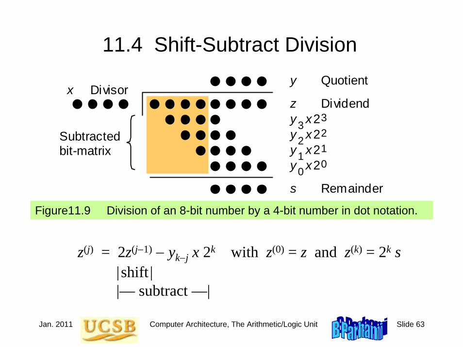
Jan. 2011 Computer Architecture, The Arithmetic/Logic Unit Slide 63
11.4 Shift-Subtract Division
Figure11.9 Division of an 8-bit number by a 4-bit number in dot notation.
2 1
2
y
2
x 2
2
1 0
3
0
Subtracted bit-matrix
Divisor x
z(j) = 2z(j−1) − yk−j x 2k with z(0) = z and z(k) = 2k s| shift ||–– subtract ––|
Dividend z
s Remainder
Quotient y
y x 3 y x 2 y x
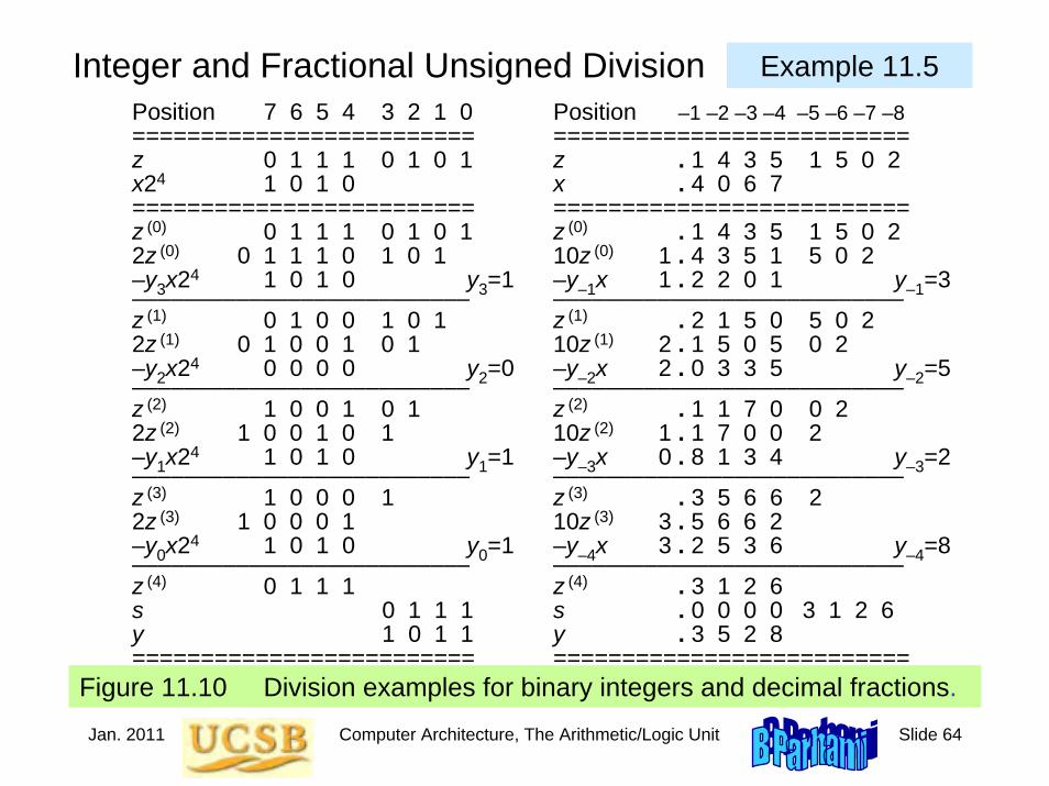
Jan. 2011 Computer Architecture, The Arithmetic/Logic Unit Slide 64
Integer and Fractional Unsigned Division
Figure 11.10 Division examples for binary integers and decimal fractions.
Position 7 6 5 4 3 2 1 0 Position –1 –2 –3 –4 –5 –6 –7 –8========================= ==========================z 0 1 1 1 0 1 0 1 z . 1 4 3 5 1 5 0 2x24 1 0 1 0 x . 4 0 6 7========================= ==========================z (0) 0 1 1 1 0 1 0 1 z (0) . 1 4 3 5 1 5 0 22z (0) 0 1 1 1 0 1 0 1 10z (0) 1 . 4 3 5 1 5 0 2–y3x24 1 0 1 0 y3=1 –y–1x 1 . 2 2 0 1 y–1=3–––––––––––––––––––––––––– –––––––––––––––––––––––––––z (1) 0 1 0 0 1 0 1 z (1) . 2 1 5 0 5 0 22z (1) 0 1 0 0 1 0 1 10z (1) 2 . 1 5 0 5 0 2–y2x24 0 0 0 0 y2=0 –y–2x 2 . 0 3 3 5 y–2=5–––––––––––––––––––––––––– –––––––––––––––––––––––––––z (2) 1 0 0 1 0 1 z (2) . 1 1 7 0 0 22z (2) 1 0 0 1 0 1 10z (2) 1 . 1 7 0 0 2–y1x24 1 0 1 0 y1=1 –y–3x 0 . 8 1 3 4 y–3=2–––––––––––––––––––––––––– –––––––––––––––––––––––––––z (3) 1 0 0 0 1 z (3) . 3 5 6 6 22z (3) 1 0 0 0 1 10z (3) 3 . 5 6 6 2–y0x24 1 0 1 0 y0=1 –y–4x 3 . 2 5 3 6 y–4=8–––––––––––––––––––––––––– –––––––––––––––––––––––––––z (4) 0 1 1 1 z (4) . 3 1 2 6s 0 1 1 1 s . 0 0 0 0 3 1 2 6y 1 0 1 1 y . 3 5 2 8========================= ==========================
Example 11.5

Jan. 2011 Computer Architecture, The Arithmetic/Logic Unit Slide 65
Division with Same-Width Operands
Figure 11.11 Division examples for 4/4-digit binary integers and fractions.
Position 7 6 5 4 3 2 1 0 Position –1 –2 –3 –4 –5 –6 –7 –8========================= ==========================z 0 0 0 0 1 1 0 1 z . 0 1 0 1x24 0 1 0 1 x . 1 1 0 1========================= ==========================z (0) 0 0 0 0 1 1 0 1 z (0) . 0 1 0 12z (0) 0 0 0 1 1 0 1 2z (0) 0 . 1 0 1 0–y3x24 0 0 0 0 y3=0 –y–1x 0 . 0 0 0 0 y–1=0–––––––––––––––––––––––––– –––––––––––––––––––––––––––z (1) 0 0 0 1 1 0 1 z (1) . 1 0 1 0 2z (1) 0 0 1 1 0 1 2z (1) 1 . 0 1 0 0–y2x24 0 0 0 0 y2=0 –y–2x 0 . 1 1 0 1 y–2=1–––––––––––––––––––––––––– –––––––––––––––––––––––––––z (2) 0 0 1 1 0 1 z (2) . 0 1 1 12z (2) 0 1 1 0 1 2z (2) 0 . 1 1 1 0 –y1x24 0 1 0 1 y1=1 –y–3x 0 . 1 1 0 1 y–3=1–––––––––––––––––––––––––– –––––––––––––––––––––––––––z (3) 0 0 0 1 1 z (3) . 0 0 0 12z (3) 0 0 1 1 2z (3) 0 . 0 0 1 0–y0x24 1 0 1 0 y0=0 –y–4x 0 . 0 0 0 0 y–4=0–––––––––––––––––––––––––– –––––––––––––––––––––––––––z (4) 0 0 1 1 z (4) . 0 0 1 0s 0 0 1 1 s . 0 0 0 0 0 0 1 0y 0 0 1 0 y . 0 1 1 0========================= ==========================
Example 11.6

Jan. 2011 Computer Architecture, The Arithmetic/Logic Unit Slide 66
Signed DivisionMethod 1 (indirect): strip operand signs, divide, set result signs
Dividend Divisor Quotient Remainderz = 5 x = 3 ⇒ y = 1 s = 2z = 5 x = –3 ⇒ y = –1 s = 2z = –5 x = 3 ⇒ y = –1 s = –2z = –5 x = –3 ⇒ y = 1 s = –2
Method 2 (direct 2’s complement): develop quotient with digits –1 and 1, chosen based on signs, convert to digits 0 and 1
Restoring division: perform trial subtraction, choose 0 for q digit if partial remainder negative
Nonrestoring division: if sign of partial remainder is correct, then subtract (choose 1 for q digit) else add (choose –1)

Jan. 2011 Computer Architecture, The Arithmetic/Logic Unit Slide 67
11.5 Hardware Dividers
Figure 11.12 Hardware divider based on the shift-subtract algorithm.
Load
Quotient y
Mux
Adder
0 1
Partial remainder z (initially z)
Divisor x
Shift
Shift
(j)
k– j
y
1
Enable
Select
Quotient
digit selector
1
out
c in
c
Trial di fference (Always subtract)
Hi Lo

Jan. 2011 Computer Architecture, The Arithmetic/Logic Unit Slide 68
The Shift Part of Shift-Subtract
Figure 11.13 Shifting incorporated in the connections to thepartial remainder register rather than as a separate phase.
To adder
From adder
Partial remainder Quotient
/ k
/ k
/ k
/ k
k–j q
MSB

Jan. 2011 Computer Architecture, The Arithmetic/Logic Unit Slide 69
High-Radix Dividers
Radix-4 division in dot notation.
Divisor x Dividend z
s Remainder
Quotient y
0, x, 2x, or 3x
z(j) = 4z(j−1) − (yk−2j+1 yk−2j)two x 2k with z(0) = z and z(k/2) = 2ks| shift ||––––––– subtract –––––––| Assume k even

Jan. 2011 Computer Architecture, The Arithmetic/Logic Unit Slide 70
Array Dividers
Figure 11.14 Array divider for 8/4-bit unsigned integers.
2 1 0 x x x
1 y
2 y
3 y 3 z
0 y
3 x
2 z
1 z
0 z
4 z 5 z 6 z 7 z
MS MS MS MS
MS MS MS MS
MS MS MS MS
MS MS MS MS
Our original dot-notation for division
Straightened dots to depict an array divider 2 1 0 s s s 3 s
0
0
0
0
b d

Jan. 2011 Computer Architecture, The Arithmetic/Logic Unit Slide 71
11.6 Programmed DivisionMiniMIPS instructions related to division
div $s0,$s1 # Lo = quotient, Hi = remainderdivu $s2,$s3 # unsigned version of divisionmfhi $t0 # set $t0 to (Hi)mflo $t1 # set $t1 to (Lo)
Compute z mod x, where z (singed) and x > 0 are integers
Divide; remainder will be obtained in Hi
if remainder is negative, then add |x| to (Hi) to obtain z mod xelse Hi holds z mod x
Example 11.7

Jan. 2011 Computer Architecture, The Arithmetic/Logic Unit Slide 72
Figure 11.15 Register usage for programmed division superimposed on the block diagram for a hardware divider.
Emulating a Hardware Divider in SoftwareExample 11.8 (MiniMIPS shift-add program for division)
Load
Quotient y
Mux
Adder
0 1
Partial remainder z (initially z)
Divisor x
Shift
Shift
(j)
k– j
y
1
Enable Select
Quotient digit
selector
1
out
c
in
c Trial difference
(Always subtract)
$t2 (counter)
$a0 (divisor x)
$a1 (quotient y)
$v1 (Lo part of z) $v0 (Hi part of z)
$t1 (bit k−j of y)
Part of the control in hardware
$t0 (MSB of Hi)
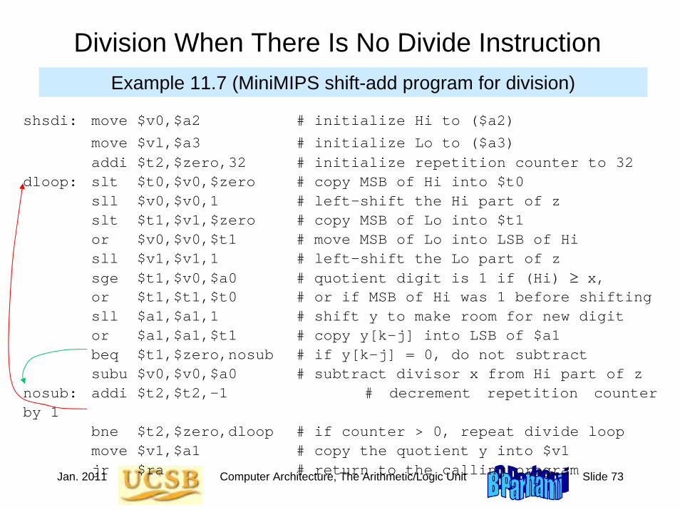
Jan. 2011 Computer Architecture, The Arithmetic/Logic Unit Slide 73
shsdi: move $v0,$a2 # initialize Hi to ($a2)
move $vl,$a3 # initialize Lo to ($a3)addi $t2,$zero,32 # initialize repetition counter to 32
dloop: slt $t0,$v0,$zero # copy MSB of Hi into $t0sll $v0,$v0,1 # left-shift the Hi part of zslt $t1,$v1,$zero # copy MSB of Lo into $t1or $v0,$v0,$t1 # move MSB of Lo into LSB of Hisll $v1,$v1,1 # left-shift the Lo part of zsge $t1,$v0,$a0 # quotient digit is 1 if (Hi) ≥ x,or $t1,$t1,$t0 # or if MSB of Hi was 1 before shiftingsll $a1,$a1,1 # shift y to make room for new digitor $a1,$a1,$t1 # copy y[k-j] into LSB of $a1beq $t1,$zero,nosub # if y[k-j] = 0, do not subtractsubu $v0,$v0,$a0 # subtract divisor x from Hi part of z
nosub: addi $t2,$t2,-1 # decrement repetition counter by 1
bne $t2,$zero,dloop # if counter > 0, repeat divide loopmove $v1,$a1 # copy the quotient y into $v1jr $ra # return to the calling program
Division When There Is No Divide InstructionExample 11.7 (MiniMIPS shift-add program for division)

Jan. 2011 Computer Architecture, The Arithmetic/Logic Unit Slide 74
Load
Quotient y
Mux
Adder
0 1
Partial remainder z (initially z)
Divisor x
Shift
Shift
(j)
k– j
y
1
Enable
Select
Quotient
digit selector
1
out
c in
c
Trial di fference (Always subtract)
Multiplier y
Mux
Adder out c
0 1
Doublewidth partial product z
Multiplicand x
Shift
Shift
(j)
j y
Add’Sub
Enable
Select
in c
Divider vs Multiplier: Hardware Similarities
2 1 0 x x x
1 y
2 y
3 y 3 z
0 y
3 x
2 z
1 z
0 z
4 z 5 z 6 z 7 z
MS MS MS MS
MS MS MS MS
MS MS MS MS
MS MS MS MS
Our original dot-notation for division
Straightened dots to depict an array divider 2 1 0 s s s 3 s
0
0
0
0
Figure 11.12 Figure 11.4
3
2
1
0
4 5 6 7
0
1
2
3
2 1 0 x x x
y
y
y
z
y
3 x
0 0
0 0
0 0
0 0
0
0
0 z
z
z
z z z z
HA FA FA
MA MA MA MA
MA MA MA MA
MA MA MA MA
MA MA MA MA
FA
0
Our o rigin al dot-n otation rep resentin g m ultiplication
S traighten ed dots to depic t array m ultiplier to the left Figure 11.14 Figure 11.7Turn upside-down

Jan. 2011 Computer Architecture, The Arithmetic/Logic Unit Slide 75
12 Floating-Point ArithmeticFloating-point is no longer reserved for high-end machines
• Multimedia and signal processing require flp arithmetic• Details of standard flp format and arithmetic operations
Topics in This Chapter
12.1 Rounding Modes
12.2 Special Values and Exceptions
12.3 Floating-Point Addition
12.4 Other Floating-Point Operations
12.5 Floating-Point Instructions
12.6 Result Precision and Errors
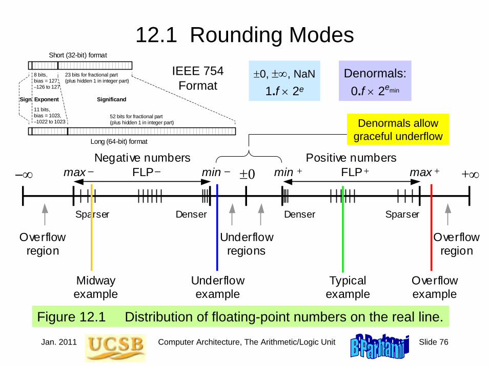
Jan. 2011 Computer Architecture, The Arithmetic/Logic Unit Slide 76
12.1 Rounding Modes
Figure 12.1 Distribution of floating-point numbers on the real line.
Denser Denser Sparser Sparser
Negative numbers FLP FLP ±0 +∞
–∞
Overflow region
Overflow region
Underflow regions
Positive numbers
Underflow example
Overflow example
Midway example
Typical example
min max min max + + – – – +
Denormals allow graceful underflow
Short (32-bit) format
Long (64-bit) format
Sign Exponent Significand
8 bits, bias = 127, –126 to 127
11 bits, bias = 1023, –1022 to 1023
52 bits for fractional part (plus hidden 1 in integer part)
23 bits for fractional part (plus hidden 1 in integer part)
IEEE 754Format
±0, ±∞, NaN1.f × 2e
Denormals:0.f × 2emin
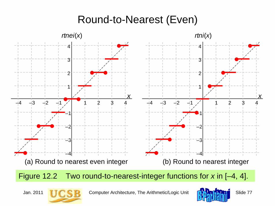
Jan. 2011 Computer Architecture, The Arithmetic/Logic Unit Slide 77
Figure 12.2 Two round-to-nearest-integer functions for x in [–4, 4].
Round-to-Nearest (Even)rtnei(x)
–4
–3
–2
–1
x–4 –3 –2 –1 4 3 2 1
4
3
2
1
rtni(x)
–4
–3
–2
–1
x–4 –3 –2 –1 4 3 2 1
4
3
2
1
(a) Round to nearest even integer (b) Round to nearest integer
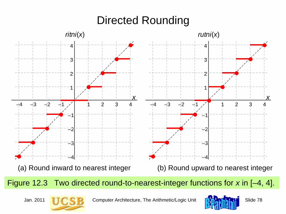
Jan. 2011 Computer Architecture, The Arithmetic/Logic Unit Slide 78
Figure 12.3 Two directed round-to-nearest-integer functions for x in [–4, 4].
Directed Rounding
(a) Round inward to nearest integer (b) Round upward to nearest integer
rutni(x)
–4
–3
–2
–1
x–4 –3 –2 –1 4 3 2 1
4
3
2
1
ritni(x)
–4
–3
–2
–1
x–4 –3 –2 –1 4 3 2 1
4
3
2
1
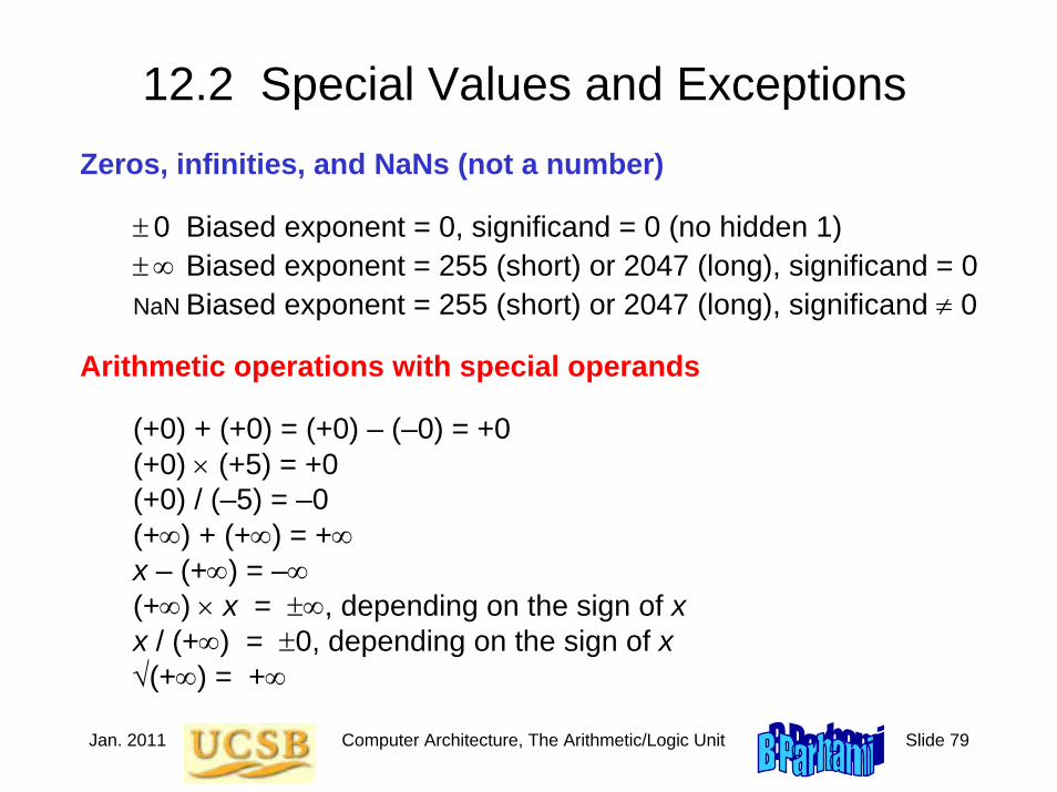
Jan. 2011 Computer Architecture, The Arithmetic/Logic Unit Slide 79
12.2 Special Values and ExceptionsZeros, infinities, and NaNs (not a number)
± 0 Biased exponent = 0, significand = 0 (no hidden 1)± ∞ Biased exponent = 255 (short) or 2047 (long), significand = 0NaN Biased exponent = 255 (short) or 2047 (long), significand ≠ 0
Arithmetic operations with special operands
(+0) + (+0) = (+0) – (–0) = +0(+0) × (+5) = +0(+0) / (–5) = –0(+∞) + (+∞) = +∞x – (+∞) = –∞(+∞) × x = ±∞, depending on the sign of xx / (+∞) = ±0, depending on the sign of x√(+∞) = +∞
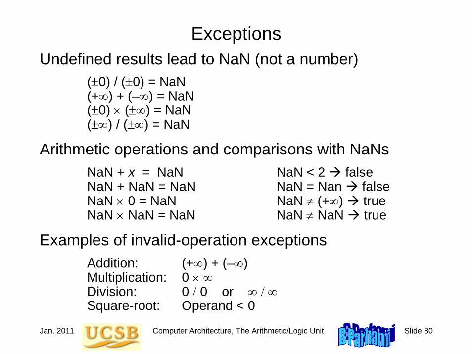
Jan. 2011 Computer Architecture, The Arithmetic/Logic Unit Slide 80
ExceptionsUndefined results lead to NaN (not a number)
(±0) / (±0) = NaN(+∞) + (–∞) = NaN(±0) × (±∞) = NaN(±∞) / (±∞) = NaN
Arithmetic operations and comparisons with NaNsNaN + x = NaN NaN < 2 falseNaN + NaN = NaN NaN = Nan falseNaN × 0 = NaN NaN ≠ (+∞) trueNaN × NaN = NaN NaN ≠ NaN true
Examples of invalid-operation exceptionsAddition: (+∞) + (–∞)Multiplication: 0 × ∞Division: 0 / 0 or ∞ / ∞Square-root: Operand < 0

Jan. 2011 Computer Architecture, The Arithmetic/Logic Unit Slide 81
12.3 Floating-Point Addition
Figure 12.4 Alignment shift and rounding in floating-point addition.
Operands after alignment shift: x = 2 1.00101101 y = 2 0.000111101101
Numbers to be added: x = 2 1.00101101 y = 2 1.11101101
5 × ×
5 × ×
Extra bits to be rounded off
Operand with smaller exponent to be preshifted
Result of addition: s = 2 1.010010111101 s = 2 1.01001100 Rounded sum
× ×
5
1
5 5
(±2e1s1) (±2e2s2)
+ (±2e1(s2 / 2e1–e2)) = ±2e1(s1 ± s2 / 2e1–e2)

Jan. 2011 Computer Architecture, The Arithmetic/Logic Unit Slide 82
Hardware for Floating-Point
Addition
Figure 12.5 Simplified schematic of a floating-point adder.
Normalize & round
Add
Align significands
Possible swap & complement
Unpack
Control & sign logic
Pack
Input 1
Output
Significands Exponents Signs
Significand Exponent Sign
Sub
±
Mu x
Input 2
Add′Sub
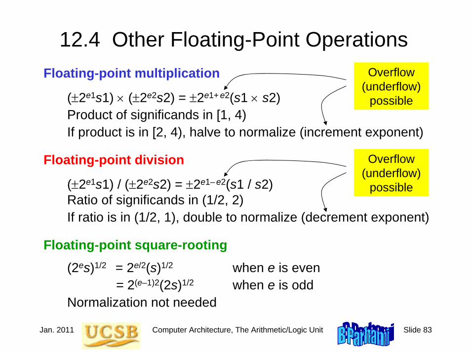
Jan. 2011 Computer Architecture, The Arithmetic/Logic Unit Slide 83
12.4 Other Floating-Point OperationsFloating-point multiplication
(±2e1s1) × (±2e2s2) = ±2e1+ e2(s1 × s2)Product of significands in [1, 4)If product is in [2, 4), halve to normalize (increment exponent)
Floating-point division
(±2e1s1) / (±2e2s2) = ±2e1– e2(s1 / s2)Ratio of significands in (1/2, 2)If ratio is in (1/2, 1), double to normalize (decrement exponent)
Floating-point square-rooting
(2es)1/2 = 2e/2(s)1/2 when e is even= 2(e–1)2(2s)1/2 when e is odd
Normalization not needed
Overflow (underflow)
possible
Overflow (underflow)
possible

Jan. 2011 Computer Architecture, The Arithmetic/Logic Unit Slide 84
Hardware for Floating-Point Multiplication and Division
Figure 12.6 Simplified schematic of a floating-point multiply/divide unit.
Normalize & round
Multiply or divide
Unpack
Control & sign logic
Mul′Div
Pack
Input 1
Output
Significands Exponents Signs
Significand Exponent Sign
±
±
Input 2

Jan. 2011 Computer Architecture, The Arithmetic/Logic Unit Slide 85
12.5 Floating-Point InstructionsFloating-point arithmetic instructions for MiniMIPS:
add.s $f0,$f8,$f10 # set $f0 to ($f8) +fp ($f10)sub.d $f0,$f8,$f10 # set $f0 to ($f8) –fp ($f10)mul.d $f0,$f8,$f10 # set $f0 to ($f8) ×fp ($f10)div.s $f0,$f8,$f10 # set $f0 to ($f8) /fp ($f10)neg.s $f0,$f8 # set $f0 to –($f8)
Figure 12.7 The common floating-point instruction format for MiniMIPS and components for arithmetic instructions. The extension (ex) field distinguishes single (* = s) from double (* = d) operands.
x x x x 0 1 1 0 0 0 0 0 0 0 0 0 0 0 0 0 0 1 1 1 0 0 0 0 0 0 0 0 31 25 20 15 0
Floating-point instruction
s = 0 d = 1
Source register 2
op ex ft
F fs fd
10 5 fn
Destination register
add.* = 0 sub.* = 1 mul.* = 2 div.* = 3 neg.* = 7
Source register 1

Jan. 2011 Computer Architecture, The Arithmetic/Logic Unit Slide 86
The Floating-Point Unit in MiniMIPS
Figure 5.1 Memory and processing subsystems for MiniMIPS.
Memory up to 2 words 30
Loc 0 Loc 4 Loc 8
Loc m − 4
Loc m − 8
4 B / location
m ≤ 2 32
$0 $1 $2
$31
Hi Lo
ALU
$0 $1 $2
$31 FP
arith
EPC Cause
BadVaddr Status
EIU FPU
TMU
Execution & integer unit
Floating- point unit
Trap & memory unit
. . .
. . .
(Coproc. 1)
(Coproc. 0)
(Main proc.)
Integer mul/div
Chapter 10
Chapter 11
Chapter 12
Pairs of registers, beginning with an even-numbered one, are used for double operands
Coprocessor 1

Jan. 2011 Computer Architecture, The Arithmetic/Logic Unit Slide 87
Floating-Point Format ConversionsMiniMIPS instructions for number format conversion:
cvt.s.w $f0,$f8 # set $f0 to single(integer $f8)cvt.d.w $f0,$f8 # set $f0 to double(integer $f8)cvt.d.s $f0,$f8 # set $f0 to double($f8)cvt.s.d $f0,$f8 # set $f0 to single($f8,$f9)cvt.w.s $f0,$f8 # set $f0 to integer($f8)cvt.w.d $f0,$f8 # set $f0 to integer($f8,$f9)
Figure 12.8 Floating-point instructions for format conversion in MiniMIPS.
1 0 0 x x x x 0 1 1 0 0 0 0 0 0 0 0 0 0 0 0 0 0 1 0 0 0 0 0 0 0 31 25 20 15 0
Floating-point instruction
*.w = 0 w.s = 0 w.d = 1 *.* = 1
Unused
op ex ft
F fs fd
10 5 fn
Destination register
To format: s = 32 d = 33 w = 36
Source register

Jan. 2011 Computer Architecture, The Arithmetic/Logic Unit Slide 88
Floating-Point Data TransfersMiniMIPS instructions for floating-point load, store, and move:
lwc1 $f8,40($s3) # load mem[40+($s3)] into $f8swc1 $f8,A($s3) # store ($f8) into mem[A+($s3)]mov.s $f0,$f8 # load $f0 with ($f8)mov.d $f0,$f8 # load $f0,$f1 with ($f8,$f9)mfc1 $t0,$f12 # load $t0 with ($f12)mtc1 $f8,$t4 # load $f8 with ($t4)
Figure 12.9 Instructions for floating-point data movement in MiniMIPS.
0 1 1 0 0 x 0 1 1 0 0 0 0 0 0 0 0 0 0 0 0 0 0 1 0 0 0 0 0 0 0 0 31 25 20 15 0
Floating-point instruction
s = 0 d = 1
Unused
op ex ft
F fs fd
10 5 fn
Destination register
mov.* = 6
Source register
1 1 1 0 0 0 0 x 0 1 1 0 0 0 0 0 0 0 0 0 0 0 0 0 0 0 0 0 0 0 0 0 31 25 20 15 0
Floating-point instruction
mfc1 = 0 mtc1 = 4
Unused
op rs rt
R rd sh
10 5 fn
Destination register
Source register
Unused

Jan. 2011 Computer Architecture, The Arithmetic/Logic Unit Slide 89
Floating-Point Branches and ComparisonsMiniMIPS instructions for floating-point load, store, and move:
bc1t L # branch on fp flag truebc1f L # branch on fp flag falsec.eq.* $f0,$f8 # if ($f0)=($f8), set flag to “true”c.lt.* $f0,$f8 # if ($f0)<($f8), set flag to “true”c.le.* $f0,$f8 # if ($f0)≤($f8), set flag to “true”
Figure 12.10 Floating-point branch and comparison instructions in MiniMIPS.
x
0 0 1 0 0 0 0 0 0 0 0 0 0 0 0 0 1 1 1 1 1 0 0 1 1 0 0 0 0 0 0 31 25 20 15 0
Floating-point instruction
true = 1 false = 0
bc1? = 8
Offset
op rs rt operand / offset
I
1 0 0 1 1 0 0 x 0 1 1 0 0 0 0 0 0 0 0 0 0 0 0 0 0 0 0 0 0 0 0 0 31 25 20 15 0
Floating-point instruction
s = 0 d = 1
Source register 2
op ex ft
F fs fd
10 5 fn
Unused c.eq.* = 50 c.lt.* = 60 c.le.* = 62
Source register 1
Correction: 1 1 x x x 0

Jan. 2011 Computer Architecture, The Arithmetic/Logic Unit Slide 90
Floating-Point Instructions of
MiniMIPS
Instruction UsageMove s/d registers mov.* fd,fs
Move fm coprocessor 1 mfc1 rt,rd
Move to coprocessor 1 mtc1 rd,rt
Add single/double add.* fd,fs,ft
Subtract single/double sub.* fd,fs,ft
Multiply single/double mul.* fd,fs,ft
Divide single/double div.* fd,fs,ft
Negate single/double neg.* fd,fs
Compare equal s/d c.eq.* fs,ft
Compare less s/d c.lt.* fs,ft
Compare less or eq s/d c.le.* fs,ft
Convert integer to single cvt.s.w fd,fs
Convert integer to double cvt.d.w fd,fs
Convert single to double cvt.d.s fd,fs
Convert double to single cvt.s.d fd,fs
Convert single to integer cvt.w.s fd,fs
Convert double to integer cvt.w.d fd,fs
Load word coprocessor 1 lwc1 ft,imm(rs)
Store word coprocessor 1 swc1 ft,imm(rs)
Branch coproc 1 true bc1t L
Branch coproc 1 false bc1f L
Copy
Control transfer
Conversions
Memory access
Arithmetic
ex#04########001101
rsrs88
fn6
01237
506062323333323636
Table 12.1
* s/d for single/double# 0/1 for single/double

Jan. 2011 Computer Architecture, The Arithmetic/Logic Unit Slide 91
12.6 Result Precision and ErrorsExample 12.4
Laws of algebra may not hold in floating-point arithmetic. For example, the following computations show that the associative law of addition, (a + b) + c = a + (b + c), is violated for the three numbers shown.
Compute a + b 2 × 0.00000011 a+b = 2 × 1.10000000 c =-2 × 1.01100101
Numbers to be added first a =-2 × 1.10101011 b = 2 × 1.10101110
5
5
Compute (a + b) + c 2 × 0.00011011 Sum = 2 × 1.10110000
5
−2 −2
−2 −6
Compute b + c (after preshifting c) 2 × 1.101010110011011 b+c = 2 × 1.10101011 (Round) a =-2 × 1.10101011
Numbers to be added first b = 2 × 1.10101110 c =-2 × 1.01100101
5
5
Compute a + (b + c) 2 × 0.00000000 Sum = 0 (Normalize to special code for 0)
5 5
5
−2
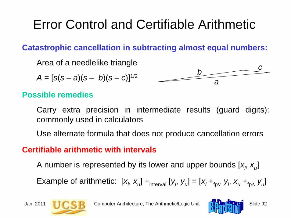
Jan. 2011 Computer Architecture, The Arithmetic/Logic Unit Slide 92
Error Control and Certifiable Arithmetic
Catastrophic cancellation in subtracting almost equal numbers:
Area of a needlelike triangle
A = [s(s – a)(s – b)(s – c)]1/2
Possible remedies
Carry extra precision in intermediate results (guard digits): commonly used in calculators
Use alternate formula that does not produce cancellation errors
Certifiable arithmetic with intervals
A number is represented by its lower and upper bounds [xl, xu]
Example of arithmetic: [xl, xu] +interval [yl, yu] = [xl +fp∇ yl, xu +fpΔ yu]
ab c
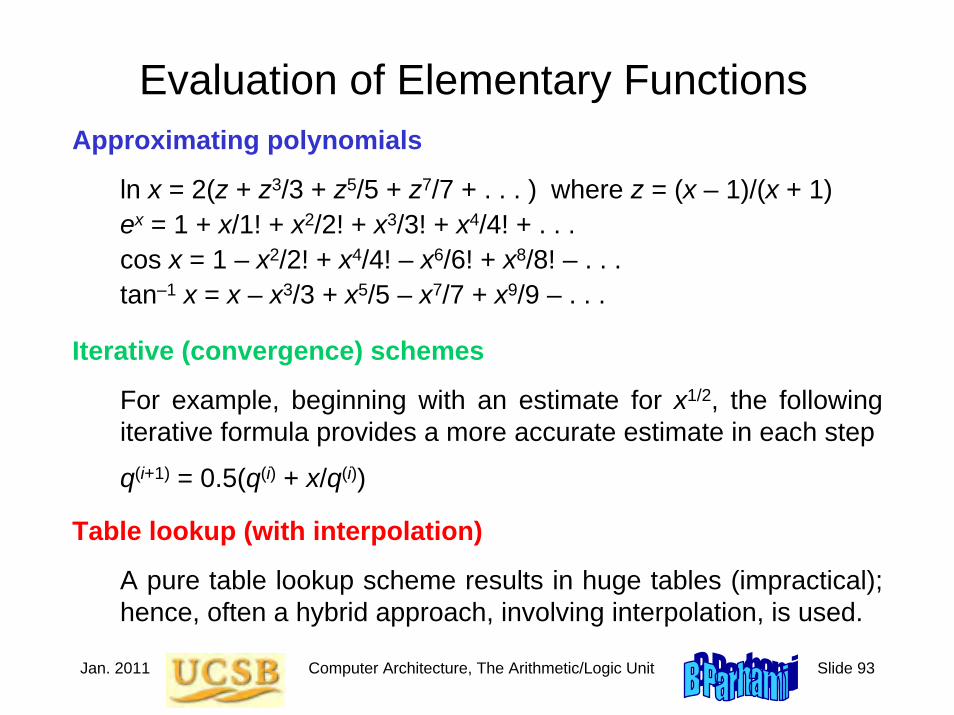
Jan. 2011 Computer Architecture, The Arithmetic/Logic Unit Slide 93
Evaluation of Elementary FunctionsApproximating polynomials
ln x = 2(z + z3/3 + z5/5 + z7/7 + . . . ) where z = (x – 1)/(x + 1)ex = 1 + x/1! + x2/2! + x3/3! + x4/4! + . . . cos x = 1 – x2/2! + x4/4! – x6/6! + x8/8! – . . . tan–1 x = x – x3/3 + x5/5 – x7/7 + x9/9 – . . .
Iterative (convergence) schemes
For example, beginning with an estimate for x1/2, the following iterative formula provides a more accurate estimate in each step
q(i+1) = 0.5(q(i) + x/q(i))
Table lookup (with interpolation)
A pure table lookup scheme results in huge tables (impractical);hence, often a hybrid approach, involving interpolation, is used.

Jan. 2011 Computer Architecture, The Arithmetic/Logic Unit Slide 94
Figure 12.12 Function evaluation by table lookup and linear interpolation.
L
Function Evaluation by Table Lookup
Add
x
Table for a
Output
Table for b
x Input x H L
f(x)
Multiply
h bits k - h bits
x H
f(x) x
x
Best linear approximationin subinterval
The linear approximation above is characterized by the line equation a + b x , where a and b are read out from tables based on x
L
H

Feb. 2011 Computer Architecture, Data Path and Control Slide 1
Part IVData Path and Control

Feb. 2011 Computer Architecture, Data Path and Control Slide 2
About This PresentationThis presentation is intended to support the use of the textbookComputer Architecture: From Microprocessors to Supercomputers, Oxford University Press, 2005, ISBN 0-19-515455-X. It is updated regularly by the author as part of his teaching of the upper-division course ECE 154, Introduction to Computer Architecture, at the University of California, Santa Barbara. Instructors can use these slides freely in classroom teaching and for other educational purposes. Any other use is strictly prohibited. © Behrooz Parhami
Edition Released Revised Revised Revised RevisedFirst July 2003 July 2004 July 2005 Mar. 2006 Feb. 2007
Feb. 2008 Feb. 2009 Feb. 2011
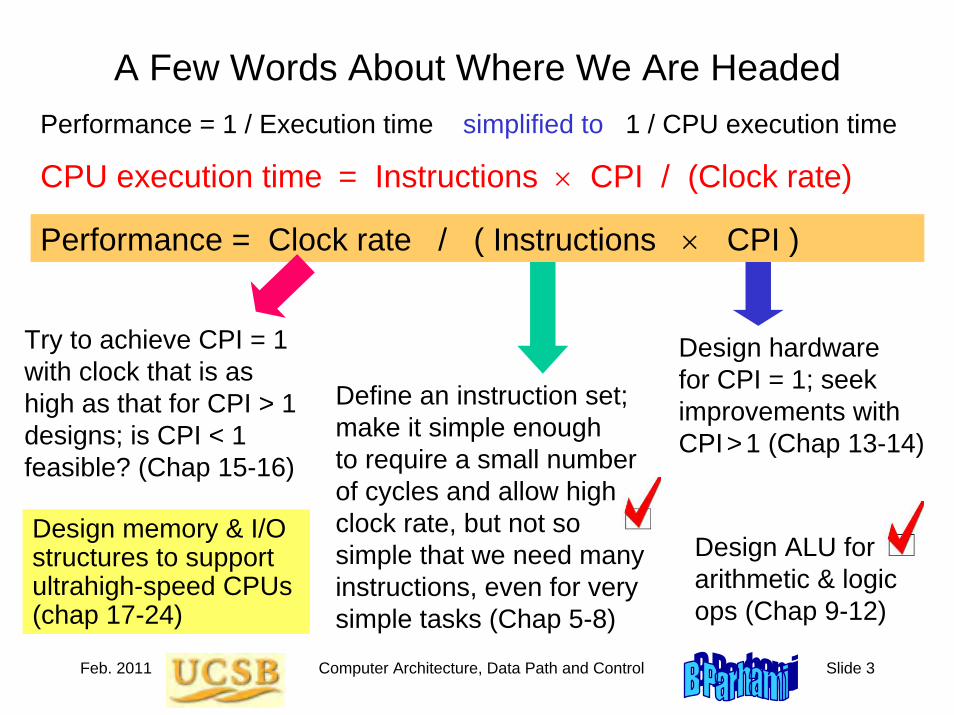
Feb. 2011 Computer Architecture, Data Path and Control Slide 3
A Few Words About Where We Are HeadedPerformance = 1 / Execution time simplified to 1 / CPU execution time
CPU execution time = Instructions × CPI / (Clock rate)
Performance = Clock rate / ( Instructions × CPI )
Define an instruction set;make it simple enough to require a small number of cycles and allow high clock rate, but not so simple that we need many instructions, even for very simple tasks (Chap 5-8)
Design hardware for CPI = 1; seek improvements with CPI >1 (Chap 13-14)
Design ALU for arithmetic & logic ops (Chap 9-12)
Try to achieve CPI = 1 with clock that is as high as that for CPI > 1 designs; is CPI < 1 feasible? (Chap 15-16)
Design memory & I/O structures to support ultrahigh-speed CPUs(chap 17-24)
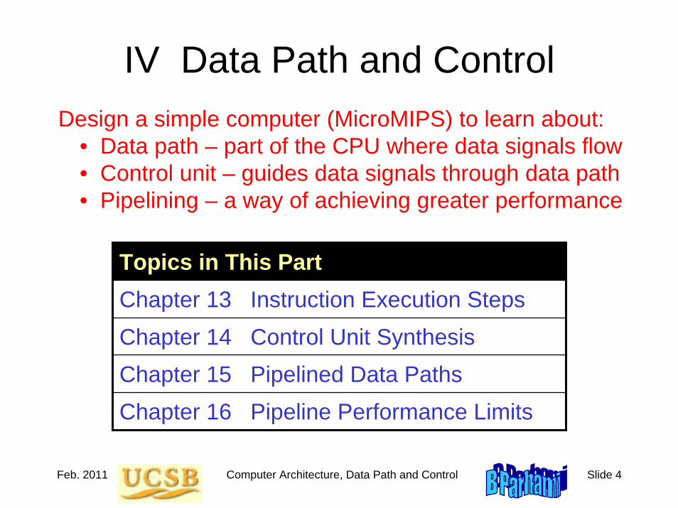
Feb. 2011 Computer Architecture, Data Path and Control Slide 4
IV Data Path and Control
Topics in This PartChapter 13 Instruction Execution StepsChapter 14 Control Unit SynthesisChapter 15 Pipelined Data PathsChapter 16 Pipeline Performance Limits
Design a simple computer (MicroMIPS) to learn about:• Data path – part of the CPU where data signals flow• Control unit – guides data signals through data path• Pipelining – a way of achieving greater performance

Feb. 2011 Computer Architecture, Data Path and Control Slide 5
13 Instruction Execution StepsA simple computer executes instructions one at a time
• Fetches an instruction from the loc pointed to by PC• Interprets and executes the instruction, then repeats
Topics in This Chapter
13.1 A Small Set of Instructions
13.2 The Instruction Execution Unit
13.3 A Single-Cycle Data Path
13.4 Branching and Jumping
13.5 Deriving the Control Signals
13.6 Performance of the Single-Cycle Design

Feb. 2011 Computer Architecture, Data Path and Control Slide 6
13.1 A Small Set of Instructions
Fig. 13.1 MicroMIPS instruction formats and naming of the various fields.
5 bits 5 bits 31 25 20 15 0
Opcode Source 1 or base
Source 2 or dest’n
op rs rt
R 6 bits 5 bits
rd
5 bits
sh
6 bits 10 5
fn
jta Jump target address, 26 bits
imm Operand / Offset, 16 bits
Destination Unused Opcode ext I
J inst
Instruction, 32 bits
Seven R-format ALU instructions (add, sub, slt, and, or, xor, nor)Six I-format ALU instructions (lui, addi, slti, andi, ori, xori)Two I-format memory access instructions (lw, sw)Three I-format conditional branch instructions (bltz, beq, bne)Four unconditional jump instructions (j, jr, jal, syscall)
We will refer to this diagram later
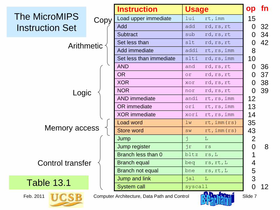
Feb. 2011 Computer Architecture, Data Path and Control Slide 7
The MicroMIPS Instruction Set
Instruction UsageLoad upper immediate lui rt,imm
Add add rd,rs,rt
Subtract sub rd,rs,rt
Set less than slt rd,rs,rt
Add immediate addi rt,rs,imm
Set less than immediate slti rd,rs,imm
AND and rd,rs,rt
OR or rd,rs,rt
XOR xor rd,rs,rt
NOR nor rd,rs,rt
AND immediate andi rt,rs,imm
OR immediate ori rt,rs,imm
XOR immediate xori rt,rs,imm
Load word lw rt,imm(rs)
Store word sw rt,imm(rs)
Jump j L
Jump register jr rs
Branch less than 0 bltz rs,L
Branch equal beq rs,rt,L
Branch not equal bne rs,rt,L
Jump and link jal L
System call syscall
Copy
Control transfer
Logic
Arithmetic
Memory access
op15
0008
100000
1213143543
2014530
fn
323442
36373839
8
12Table 13.1

Feb. 2011 Computer Architecture, Data Path and Control Slide 8
13.2 The Instruction Execution Unit
Fig. 13.2 Abstract view of the instruction execution unit for MicroMIPS. For naming of instruction fields, see Fig. 13.1.
ALU
Data cache
Instr cache
Next addr
Control
Reg file
op
jta
fn
inst
imm
rs,rt,rd (rs)
(rt)
Address Data
PC
5 bits 5 bits 31 25 20 15 0
Opcode Source 1 or base
Source 2 or dest’n
op rs rt
R 6 bits 5 bits
rd
5 bits
sh
6 bits 10 5
fn
jta Jump target address, 26 bits
imm Operand / Offset, 16 bits
Destination Unused Opcode ext I
J inst
Instruction, 32 bits
bltz,jr
beq,bne
12 A/L, lui, lw,sw
j,jal
syscall
22 instructions
Harvardarchitecture

Feb. 2011 Computer Architecture, Data Path and Control Slide 9
13.3 A Single-Cycle Data Path
Fig. 13.3 Key elements of the single-cycle MicroMIPS data path.
/
ALU
Data cache
Instr cache
Next addr
Reg file
op
jta
fn
inst
imm
rs (rs)
(rt)
Data addr
Data in 0
1
ALUSrc ALUFunc DataWrite
DataRead
SE
RegInSrc
rt
rd
RegDst RegWrite
32 / 16
Register input
Data out
Func
ALUOvfl
Ovfl
31
0 1 2
Next PC
Incr PC
(PC)
Br&Jump
ALU out
PC
0 1 2
Register writeback
Instruction fetch Reg access / decode ALU operation Data access

Feb. 2011 Computer Architecture, Data Path and Control Slide 10
An ALU for MicroMIPS
Fig. 10.19 A multifunction ALU with 8 control signals (2 for function class, 1 arithmetic, 3 shift, 2 logic) specifying the operation.
Add′Sub
x ± y
y
x
Adder
c 32
c 0
k /
Shifter
Logic unit
s
Logic function
Amount
5
2
Constant amount
Variable amount
5
5
Const′Var
0
1
0
1
2
3
Function class
2
Shift function
5 LSBs Shifted y
32
32
32
2
c 31
32-input NOR
Ovfl Zero
32 32
MSB
ALU
y
x
s
Shorthand symbol for ALU
Ovfl Zero
Func
Control
0 or 1
AND 00 OR 01
XOR 10 NOR 11
00 Shift 01 Set less 10 Arithmetic 11 Logic
00 No shift 01 Logical left 10 Logical right 11 Arith right
lui
imm
We use only 5 control signals
(no shifts)
5

Feb. 2011 Computer Architecture, Data Path and Control Slide 11
13.4 Branching and Jumping
Fig. 13.4 Next-address logic for MicroMIPS (see top part of Fig. 13.3). Adder
jta imm
(rs)
(rt)
SE
SysCallAddr
PCSrc
(PC)
Branch condition checker
in c
1 0 1 2 3
/ 30
/ 32 BrTrue / 32
/ 30 / 30
/ 30
/ 30
/ 30
/ 30 / 26
/ 30
/ 30 4 MSBs
30 MSBs
BrType
IncrPC
NextPC
/ 30 31:2
16
(PC)31:2 + 1 Default option(PC)31:2 + 1 + imm When instruction is branch and condition is met(PC)31:28 | jta When instruction is j or jal(rs)31:2 When the instruction is jrSysCallAddr Start address of an operating system routine
Update options for PC
Lowest 2 bits of PC always 00
4 MSBs
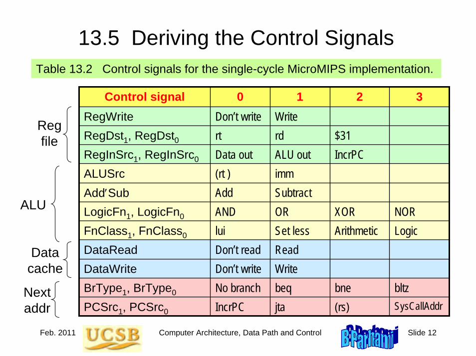
Feb. 2011 Computer Architecture, Data Path and Control Slide 12
13.5 Deriving the Control SignalsTable 13.2 Control signals for the single-cycle MicroMIPS implementation.
Control signal 0 1 2 3RegWrite Don’t write WriteRegDst1, RegDst0 rt rd $31RegInSrc1, RegInSrc0 Data out ALU out IncrPCALUSrc (rt ) immAdd′Sub Add SubtractLogicFn1, LogicFn0 AND OR XOR NORFnClass1, FnClass0 lui Set less Arithmetic LogicDataRead Don’t read ReadDataWrite Don’t write WriteBrType1, BrType0 No branch beq bne bltzPCSrc1, PCSrc0 IncrPC jta (rs) SysCallAddr
Reg file
Data cache
Next addr
ALU

Feb. 2011 Computer Architecture, Data Path and Control Slide 13
Single-Cycle Data Path, Repeated for Reference
Fig. 13.3 Key elements of the single-cycle MicroMIPS data path.
/
ALU
Data cache
Instr cache
Next addr
Reg file
op
jta
fn
inst
imm
rs (rs)
(rt)
Data addr
Data in 0
1
ALUSrc ALUFunc DataWrite
DataRead
SE
RegInSrc
rt
rd
RegDst RegWrite
32 / 16
Register input
Data out
Func
ALUOvfl
Ovfl
31
0 1 2
Next PC
Incr PC
(PC)
Br&Jump
ALU out
PC
0 1 2
Register writeback
Outcome of an executed instruction:A new value loaded into PCPossible new value in a reg or memory loc
Instruction fetch Reg access / decode ALU operation Data access
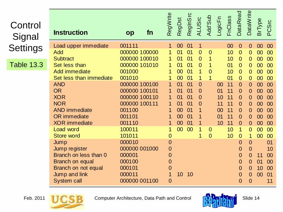
Feb. 2011 Computer Architecture, Data Path and Control Slide 14
Control Signal
Settings
Table 13.3
Load upper immediate Add Subtract Set less than Add immediate Set less than immediate AND OR XOR NOR AND immediate OR immediate XOR immediate Load word Store word Jump Jump register Branch on less than 0 Branch on equal Branch on not equal Jump and link System call
001111 000000 100000 000000 100010 000000 101010 001000 001010 000000 100100 000000 100101 000000 100110 000000 100111 001100 001101 001110 100011 101011 000010 000000 001000 000001 000100 000101 000011 000000 001100
1 1 1 1 1 1 1 1 1 1 1 1 1 1 0 0 0 0 0 0 1 0
op fn
00 01 01 01 00 00 01 01 01 01 00 00 00 00
10
01 01 01 01 01 01 01 01 01 01 01 01 01 00
10
1 0 0 0 1 1 0 0 0 0 1 1 1 1 1
0 1 1 0 1 0 0
00 01 10 11 00 01 10
00 10 10 01 10 01 11 11 11 11 11 11 11 10 10
0 0 0 0 0 0 0 0 0 0 0 0 0 1 0 0 0 0 0 0 0 0
0 0 0 0 0 0 0 0 0 0 0 0 0 0 1 0 0 0 0 0 0 0
00 00 00 00 00 00 00 00 00 00 00 00 00 00 00
11 0110 00
00 00 00 00 00 00 00 00 00 00 00 00 00 00 00 01 10 00 00 00 01 11
Instruction Reg
Writ
e
Reg
Dst
Reg
InS
rc
ALU
Src
Add
’Sub
Logi
cFn
FnC
lass
Dat
aRea
d
Dat
aWrit
e
BrT
ype
PC
Src

Feb. 2011 Computer Architecture, Data Path and Control Slide 15
Control Signals in the Single-Cycle Data Path
Fig. 13.3 Key elements of the single-cycle MicroMIPS data path.
/
ALU
Data cache
Instr cache
Next addr
Reg file
op
jta
fn
inst
imm
rs (rs)
(rt)
Data addr
Data in 0
1
ALUSrc ALUFunc DataWrite
DataRead
SE
RegInSrc
rt
rd
RegDst RegWrite
32 / 16
Register input
Data out
Func
ALUOvfl
Ovfl
31
0 1 2
Next PC
Incr PC
(PC)
Br&Jump
ALU out
PC
0 1 2
Add′Sub LogicFn FnClassPCSrc BrType
lui
001111 10001
1 x xx 00
0 0
00 00
slt
000000 10101
0 1 xx 01
0 0
00 00010101

Feb. 2011 Computer Architecture, Data Path and Control Slide 16
Instruction Decoding
Fig. 13.5 Instruction decoder for MicroMIPS built of two 6-to-64 decoders.
jrIns t
norInst
s ltIns t
orIns t xorInst
syscallIns t
andInst
addInst
subInst
RtypeInst
bltzIns t jIns t jalIns t beqInst bneInst
s ltiIns t
andiIns t oriIns t xoriIns t luiIns t
lwInst
swInst
addiIns t
1
0 1 2 3 4 5
10
12 13 14 15
35
43
63
8 op
Dec
oder
fn D
ecod
er
/ 6 / 6 op fn
0
8
12
32
34
36 37 38 39
42
63
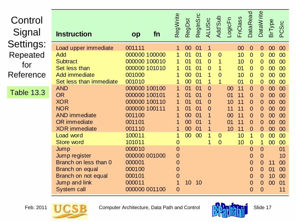
Feb. 2011 Computer Architecture, Data Path and Control Slide 17
Control Signal
Settings:Repeated
for Reference
Table 13.3
Load upper immediate Add Subtract Set less than Add immediate Set less than immediate AND OR XOR NOR AND immediate OR immediate XOR immediate Load word Store word Jump Jump register Branch on less than 0 Branch on equal Branch on not equal Jump and link System call
001111 000000 100000 000000 100010 000000 101010 001000 001010 000000 100100 000000 100101 000000 100110 000000 100111 001100 001101 001110 100011 101011 000010 000000 001000 000001 000100 000101 000011 000000 001100
1 1 1 1 1 1 1 1 1 1 1 1 1 1 0 0 0 0 0 0 1 0
op fn
00 01 01 01 00 00 01 01 01 01 00 00 00 00
10
01 01 01 01 01 01 01 01 01 01 01 01 01 00
10
1 0 0 0 1 1 0 0 0 0 1 1 1 1 1
0 1 1 0 1 0 0
00 01 10 11 00 01 10
00 10 10 01 10 01 11 11 11 11 11 11 11 10 10
0 0 0 0 0 0 0 0 0 0 0 0 0 1 0 0 0 0 0 0 0 0
0 0 0 0 0 0 0 0 0 0 0 0 0 0 1 0 0 0 0 0 0 0
00 00 00 00 00 00 00 00 00 00 00 00 00 00 00
11 0110 00
00 00 00 00 00 00 00 00 00 00 00 00 00 00 00 01 10 00 00 00 01 11
Instruction Reg
Writ
e
Reg
Dst
Reg
InS
rc
ALU
Src
Add
’Sub
Logi
cFn
FnC
lass
Dat
aRea
d
Dat
aWrit
e
BrT
ype
PC
Src
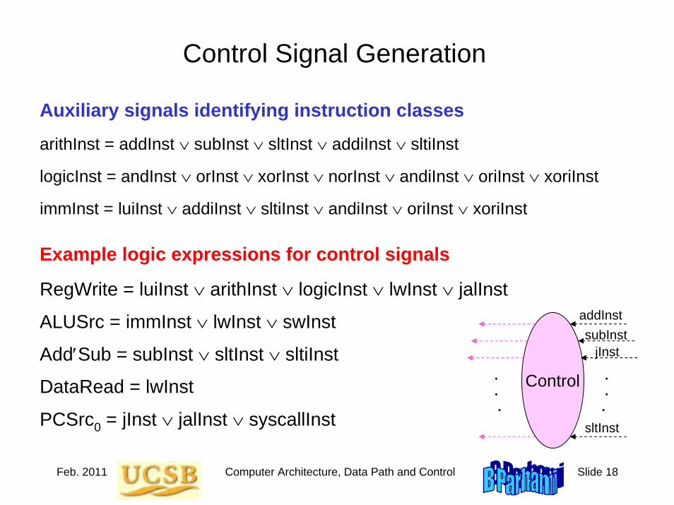
Feb. 2011 Computer Architecture, Data Path and Control Slide 18
Control Signal Generation
Auxiliary signals identifying instruction classes
arithInst = addInst ∨ subInst ∨ sltInst ∨ addiInst ∨ sltiInst
logicInst = andInst ∨ orInst ∨ xorInst ∨ norInst ∨ andiInst ∨ oriInst ∨ xoriInst
immInst = luiInst ∨ addiInst ∨ sltiInst ∨ andiInst ∨ oriInst ∨ xoriInst
Example logic expressions for control signals
RegWrite = luiInst ∨ arithInst ∨ logicInst ∨ lwInst ∨ jalInst
ALUSrc = immInst ∨ lwInst ∨ swInst
Add′Sub = subInst ∨ sltInst ∨ sltiInst
DataRead = lwInst
PCSrc0 = jInst ∨ jalInst ∨ syscallInst
Control
addInstsubInst
jInst
sltInst
.
..
.
..

Feb. 2011 Computer Architecture, Data Path and Control Slide 19
Putting It All Together
/
ALU
Data cache
Instr cache
Next addr
Reg file
op
jta
fn
inst
imm
rs (rs)
(rt)
Data addr
Data in 0
1
ALUSrc ALUFunc DataWrite
DataRead
SE
RegInSrc
rt
rd
RegDst RegWrite
32 / 16
Register input
Data out
Func
ALUOvfl
Ovfl
31
0 1 2
Next PC
Incr PC
(PC)
Br&Jump
ALU out
PC
0 1 2
Fig. 13.3
Control
addInstsubInst
jInst
sltInst
.
..
.
..
Fig. 10.19
Add′Sub
x ± y
y
x
Adder
c 32
c 0
k /
Shifter
Logic unit
s
Logic function
Amount
5
2
Constant amount
Variable amount
5
5
Const′Var
0
1
0
1
2
3
Function class
2
Shift function
5 LSBs Shifted y
32
32
32
2
c 31
32-input NOR
Ovfl Zero
32 32
MSB
A
y
x
Shorthsymbfor AL
OZero
Fun
Cont
0 or 1
AND 00 OR 01
XOR 10 NOR 11
00 Shif t 01 Set less 10 Arithmetic 11 Logic
00 No shif t 01 Logical lef t 10 Logical right 11 Arith right
imm
lui
Adder
jta imm
(rs)
(rt)
SE
SysCallAddr
PCSrc
(PC)
Branch condition checker
in c
1 0 1 2 3
/ 30
/ 32 BrTrue / 32
/ 30 / 30
/ 30
/ 30
/ 30
/ 30 / 26
/ 30
/ 30 4 MSBs
30 MSBs
BrType
IncrPC
NextPC
/ 30 31:2
16
Fig. 13.4
4 MSBs

Feb. 2011 Computer Architecture, Data Path and Control Slide 20
13.6 Performance of the Single-Cycle DesignAn example combinational-logic data path to compute z := (u + v)(w – x) / y
Add/Sub latency
2 ns
Multiply latency
6 ns
Divide latency15 ns
Beginning with inputs u, v, w, x, and y stored in registers, the entire computation can be completed in ≅25 ns, allowing 1 ns each for register readout and write
Total latency23 ns
Note that the divider gets its correct inputs after ≅9 ns, but this won’t cause a problem if we allow enough total time
×
/
+
−
y
u
v
w
xz
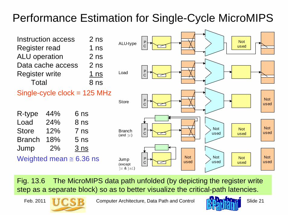
Feb. 2011 Computer Architecture, Data Path and Control Slide 21
Performance Estimation for Single-Cycle MicroMIPS
Fig. 13.6 The MicroMIPS data path unfolded (by depicting the register write step as a separate block) so as to better visualize the critical-path latencies.
Instruction access 2 nsRegister read 1 nsALU operation 2 nsData cache access 2 nsRegister write 1 ns
Total 8 nsSingle-cycle clock = 125 MHz
P C
P C
P C
P C
P C
ALU-type
Load
Store
Branch
Jump
Not used
Not used
Not used
Not used
Not used
Not used
Not used
Not used
Not used
(and jr)
(except jr & jal)
R-type 44% 6 nsLoad 24% 8 nsStore 12% 7 nsBranch 18% 5 nsJump 2% 3 nsWeighted mean ≅ 6.36 ns

Feb. 2011 Computer Architecture, Data Path and Control Slide 22
How Good is Our Single-Cycle Design?
Instruction access 2 nsRegister read 1 nsALU operation 2 nsData cache access 2 nsRegister write 1 ns
Total 8 nsSingle-cycle clock = 125 MHz
Clock rate of 125 MHz not impressive
How does this compare with current processors on the market?
Not bad, where latency is concerned
A 2.5 GHz processor with 20 or so pipeline stages has a latency of about
0.4 ns/cycle × 20 cycles = 8 ns
Throughput, however, is much better for the pipelined processor:
Up to 20 times better with single issue
Perhaps up to 100 times better with multiple issue

Feb. 2011 Computer Architecture, Data Path and Control Slide 23
14 Control Unit SynthesisThe control unit for the single-cycle design is memoryless
• Problematic when instructions vary greatly in complexity• Multiple cycles needed when resources must be reused
Topics in This Chapter14.1 A Multicycle Implementation
14.2 Choosing the Clock Cycle
14.3 The Control State Machine
14.4 Performance of the Multicycle Design
14.5 Microprogramming
14.6 Exception Handling

Feb. 2011 Computer Architecture, Data Path and Control Slide 24
14.1 A Multicycle Implementation
Appointment Appointment book for a book for a dentistdentist
Assume longest Assume longest treatment takes treatment takes one hourone hour
SingleSingle--cyclecycle MulticycleMulticycle

Feb. 2011 Computer Architecture, Data Path and Control Slide 25
Single-Cycle vs. Multicycle MicroMIPS
Fig. 14.1 Single-cycle versus multicycle instruction execution.
Clock
Clock
Instr 2 Instr 1 Instr 3 Instr 4 3 cycles 3 cycles 4 cycles 5 cycles
Time saved
Instr 1 Instr 4 Instr 3 Instr 2
Time needed
Time needed
Time allotted
Time allotted
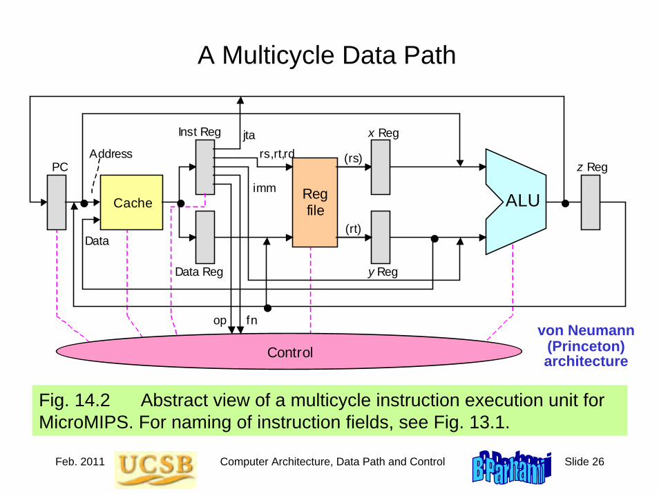
Feb. 2011 Computer Architecture, Data Path and Control Slide 26
A Multicycle Data Path
Fig. 14.2 Abstract view of a multicycle instruction execution unit for MicroMIPS. For naming of instruction fields, see Fig. 13.1.
ALU
Cache
Control
Reg file
op
jta
fn
imm
rs,rt,rd (rs)
(rt)
Address
Data
Inst Reg
Data Reg
x Reg
y Reg
z Reg PC
von Neumann (Princeton)architecture
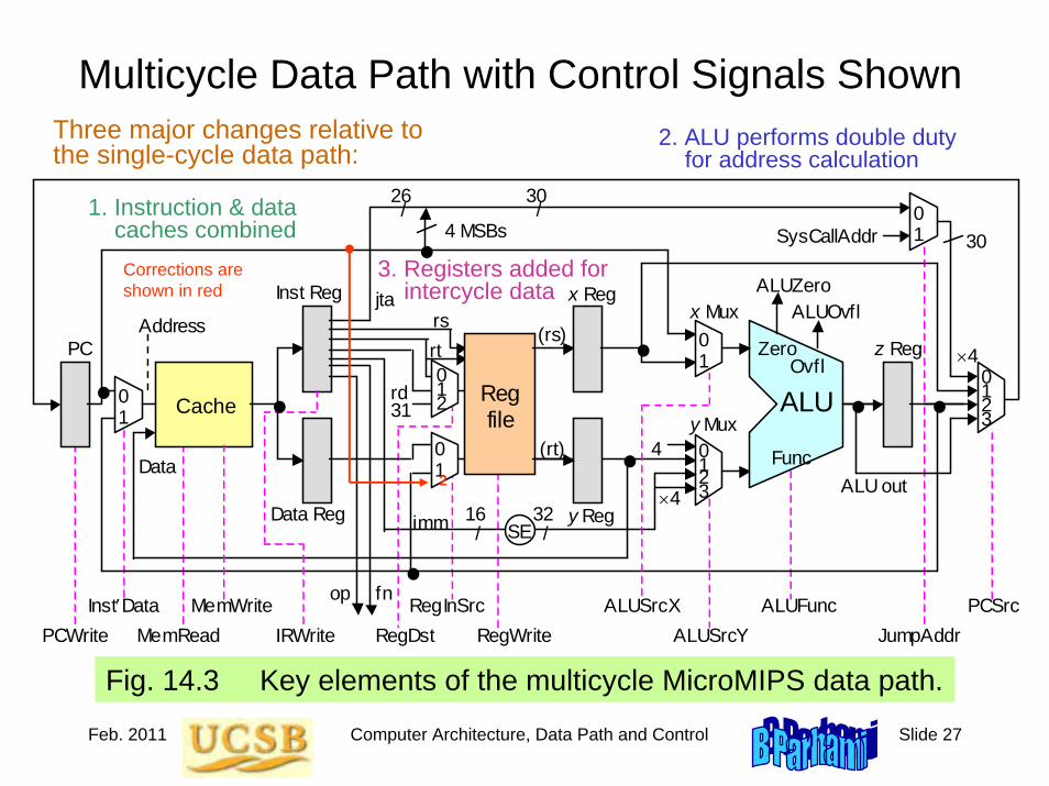
Feb. 2011 Computer Architecture, Data Path and Control Slide 27
Multicycle Data Path with Control Signals Shown
Fig. 14.3 Key elements of the multicycle MicroMIPS data path.
Three major changes relative to the single-cycle data path:
1. Instruction & data caches combined
2. ALU performs double duty for address calculation
3. Registers added for intercycle data
/
16
rs
0 1
0 1 2
ALU
Cache Reg file
op
jta
fn
(rs)
(rt)
Address
Data
Inst Reg
Data Reg
x Reg
y Reg
z Reg PC
×4
ALUSrcX
ALUFunc
MemWrite MemRead
RegInSrc
4
rd
RegDst RegWrite
/
32
Func
ALUOvfl
Ovfl
31
PCSrc PCWrite IRWrite
ALU out
0 1
0 1
0 1 2 3
0 1 2 3
Inst′Data ALUSrcY
SysCallAddr
/
26
×4
rt
ALUZero
Zero
x Mux
y Mux
0 1
JumpAddr
4 MSBs
/
30
30
SE
imm
2
Corrections are shown in red

Feb. 2011 Computer Architecture, Data Path and Control Slide 28
14.2 Clock Cycle and Control SignalsTable 14.1 Control signal 0 1 2 3
JumpAddr jta SysCallAddrPCSrc1, PCSrc0 Jump addr x reg z reg ALU outPCWrite Don’t write WriteInst′Data PC z regMemRead Don’t read ReadMemWrite Don’t write Write
ALUSrcX PC x regALUSrcY1, ALUSrcY0 4 y reg imm 4 × immAdd′Sub Add SubtractLogicFn1, LogicFn0 AND OR XOR NOR
IRWrite Don’t write WriteRegWrite Don’t write WriteRegDst1, RegDst0 rt rd $31RegInSrc1, RegInSrc0 Data reg z reg PC
FnClass1, FnClass0 lui Set less Arithmetic Logic
Register file
ALU
Cache
Program counter

Feb. 2011 Computer Architecture, Data Path and Control Slide 29
Multicycle Data Path, Repeated for Reference
Fig. 14.3 Key elements of the multicycle MicroMIPS data path.
/
16
rs
0 1
0 1 2
ALU
Cache Reg file
op
jta
fn
(rs)
(rt)
Address
Data
Inst Reg
Data Reg
x Reg
y Reg
z Reg PC
×4
ALUSrcX
ALUFunc
MemWrite MemRead
RegInSrc
4
rd
RegDst RegWrite
/
32
Func
ALUOvfl
Ovfl
31
PCSrc PCWrite IRWrite
ALU out
0 1
0 1
0 1 2 3
0 1 2 3
Inst′Data ALUSrcY
SysCallAddr
/
26
×4
rt
ALUZero
Zero
x Mux
y Mux
0 1
JumpAddr
4 MSBs
/
30
30
SE
imm
2
Corrections are shown in red

Feb. 2011 Computer Architecture, Data Path and Control Slide 30
Execution Cycles
Table 14.2 Execution cycles for multicycle MicroMIPS
Instruction Operations Signal settingsAny Read out the instruction and
write it into instruction register, increment PC
Inst′Data = 0, MemRead = 1IRWrite = 1, ALUSrcX = 0ALUSrcY = 0, ALUFunc = ‘+’PCSrc = 3, PCWrite = 1
Any Read out rs & rt into x & yregisters, compute branch address and save in z register
ALUSrcX = 0, ALUSrcY = 3ALUFunc = ‘+’
ALU type Perform ALU operation and save the result in z register
ALUSrcX = 1, ALUSrcY = 1 or 2ALUFunc: Varies
Load/Store Add base and offset values, save in z register
ALUSrcX = 1, ALUSrcY = 2ALUFunc = ‘+’
Branch If (x reg) = ≠ < (y reg), set PC to branch target address
ALUSrcX = 1, ALUSrcY = 1ALUFunc= ‘−’, PCSrc = 2PCWrite = ALUZero or ALUZero′ or ALUOut31
Jump Set PC to the target address jta, SysCallAddr, or (rs)
JumpAddr = 0 or 1,PCSrc = 0 or 1, PCWrite = 1
ALU type Write back z reg into rd RegDst = 1, RegInSrc = 1RegWrite = 1
Load Read memory into data reg Inst′Data = 1, MemRead = 1Store Copy y reg into memory Inst′Data = 1, MemWrite = 1Load Copy data register into rt RegDst = 0, RegInSrc = 0
RegWrite = 1
Fetch & PC incr
Decode & reg read
ALU oper & PC update
Reg write or mem access
Reg write for lw
1
2
3
4
5

Feb. 2011 Computer Architecture, Data Path and Control Slide 31
14.3 The Control State Machine
Fig. 14.4 The control state machine for multicycle MicroMIPS.
State 0
Inst′Data = 0 MemRead = 1
IRWrite = 1 ALUSrcX = 0 ALUSrcY = 0 ALUFunc = ‘+’
PCSrc = 3 PCWrite = 1
Start
Cycle 1 Cycle 3 Cycle 2 Cycle 1 Cycle 4 Cycle 5
ALU- type
lw/ sw lw
sw
State 1
ALUSrcX = 0 ALUSrcY = 3 ALUFunc = ‘+’
State 5 ALUSrcX = 1 ALUSrcY = 1 ALUFunc = ‘−’ JumpAddr = %
PCSrc = @ PCWrite = #
State 8
RegDst = 0 or 1 RegInSrc = 1 RegWrite = 1
State 7
ALUSrcX = 1 ALUSrcY = 1 or 2 ALUFunc = Varies
State 6
Inst′Data = 1 MemWrite = 1
State 4
RegDst = 0 RegInSrc = 0 RegWrite = 1
State 2
ALUSrcX = 1 ALUSrcY = 2 ALUFunc = ‘+’
State 3
Inst′Data = 1 MemRead = 1
Jump/ Branch
Notes for State 5: % 0 for j or jal, 1 for syscall, don’t-care for other instr’s @ 0 for j, jal, and syscall, 1 for jr, 2 for branches # 1 for j, jr, jal, and syscall, ALUZero (′) for beq (bne), bit 31 of ALUout for bltz For jal, RegDst = 2, RegInSrc = 1, RegWrite = 1
Note for State 7: ALUFunc is determined based on the op and fn f ields
Speculative calculation of branch address
Branches based on instruction

Feb. 2011 Computer Architecture, Data Path and Control Slide 32
State and Instruction Decoding
Fig. 14.5 State and instruction decoders for multicycle MicroMIPS.
jrInst
norInst
sltInst
orInst xorInst
syscallInst
andInst
addInst
subInst
RtypeInst
bltzInst jInst jalInst beqInst bneInst
sltiInst
andiInst oriInst xoriInst luiInst
lwInst
swInst
andiInst
1
0 1 2 3 4 5
10
12 13 14 15
35
43
63
8
op D
ecod
er
fn D
ecod
er
/ 6 / 6 op fn
0
8
12
32
34
36 37 38 39
42
63
ControlSt0 ControlSt1 ControlSt2 ControlSt3 ControlSt4 ControlSt5
ControlSt8
ControlSt6 1
st D
ecod
er
/ 4
st
0 1 2 3 4 5
7
12 13 14 15
8 9 10
6
11
ControlSt7
addiInst

Feb. 2011 Computer Architecture, Data Path and Control Slide 33
Control Signal GenerationCertain control signals depend only on the control state
ALUSrcX = ControlSt2 ∨ ControlSt5 ∨ ControlSt7RegWrite = ControlSt4 ∨ ControlSt8
Auxiliary signals identifying instruction classes
addsubInst = addInst ∨ subInst ∨ addiInstlogicInst = andInst ∨ orInst ∨ xorInst ∨ norInst ∨ andiInst ∨ oriInst ∨ xoriInst
Logic expressions for ALU control signals
Add′Sub = ControlSt5 ∨ (ControlSt7 ∧ subInst)FnClass1 = ControlSt7′ ∨ addsubInst ∨ logicInst FnClass0 = ControlSt7 ∧ (logicInst ∨ sltInst ∨ sltiInst)LogicFn1 = ControlSt7 ∧ (xorInst ∨ xoriInst ∨ norInst)LogicFn0 = ControlSt7 ∧ (orInst ∨ oriInst ∨ norInst)
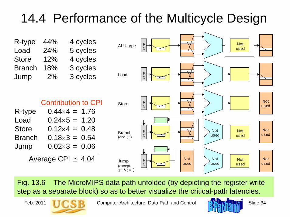
Feb. 2011 Computer Architecture, Data Path and Control Slide 34
14.4 Performance of the Multicycle Design
Fig. 13.6 The MicroMIPS data path unfolded (by depicting the register write step as a separate block) so as to better visualize the critical-path latencies.
P C
P C
P C
P C
P C
ALU-type
Load
Store
Branch
Jump
Not used
Not used
Not used
Not used
Not used
Not used
Not used
Not used
Not used
(and jr)
(except jr & jal)
R-type 44% 4 cyclesLoad 24% 5 cyclesStore 12% 4 cyclesBranch 18% 3 cyclesJump 2% 3 cycles
Contribution to CPIR-type 0.44×4 = 1.76Load 0.24×5 = 1.20Store 0.12×4 = 0.48Branch 0.18×3 = 0.54Jump 0.02×3 = 0.06
_____________________________
Average CPI ≅ 4.04
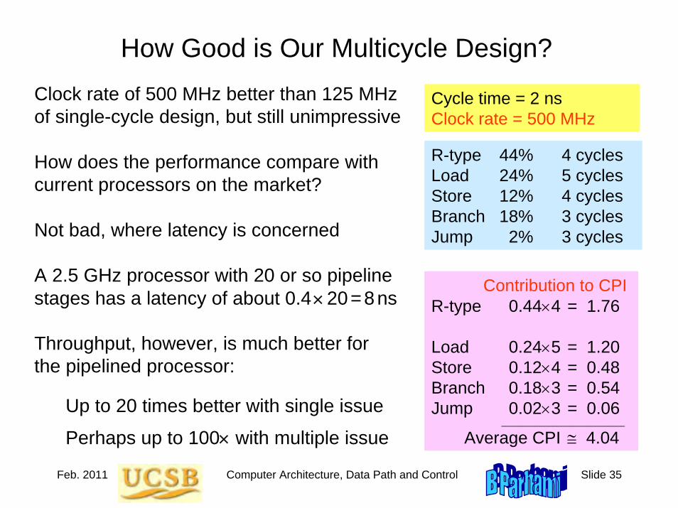
Feb. 2011 Computer Architecture, Data Path and Control Slide 35
How Good is Our Multicycle Design?Clock rate of 500 MHz better than 125 MHz of single-cycle design, but still unimpressive
How does the performance compare with current processors on the market?
Not bad, where latency is concerned
A 2.5 GHz processor with 20 or so pipeline stages has a latency of about 0.4×20=8ns
Throughput, however, is much better for the pipelined processor:
Up to 20 times better with single issue
Perhaps up to 100× with multiple issue
R-type 44% 4 cyclesLoad 24% 5 cyclesStore 12% 4 cyclesBranch 18% 3 cyclesJump 2% 3 cycles
Contribution to CPIR-type 0.44×4 = 1.76
Load 0.24×5 = 1.20Store 0.12×4 = 0.48Branch 0.18×3 = 0.54Jump 0.02×3 = 0.06
_____________________________
Average CPI ≅ 4.04
Cycle time = 2 nsClock rate = 500 MHz
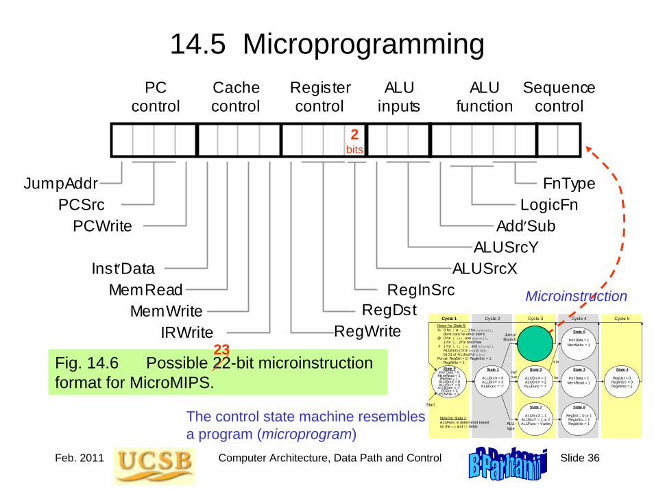
Feb. 2011 Computer Architecture, Data Path and Control Slide 36
14.5 Microprogramming
State 0
Inst′Data = 0 MemRead = 1
IRWrite = 1 ALUSrcX = 0 ALUSrcY = 0 ALUFunc = ‘+’
PCSrc = 3 PCWrite = 1
Start
Cycle 1 Cycle 3 Cycle 2 Cycle 1 Cycle 4 Cycle 5
ALU- type
lw/ sw lw
sw
State 1
ALUSrcX = 0 ALUSrcY = 3
ALUFunc = ‘+’
State 5 ALUSrcX = 1 ALUSrcY = 1 ALUFunc = ‘−’ JumpAddr = %
PCSrc = @ PCWrite = #
State 8
RegDst = 0 or 1 RegInSrc = 1 RegWrite = 1
State 7
ALUSrcX = 1 ALUSrcY = 1 or 2 ALUFunc = Varies
State 6
Inst′Data = 1 MemWrite = 1
State 4
RegDst = 0 RegInSrc = 0 RegWrite = 1
State 2
ALUSrcX = 1 ALUSrcY = 2 ALUFunc = ‘+’
State 3
Inst′Data = 1 MemRead = 1
Jump/ Branch
Notes for State 5: % 0 for j or jal, 1 for syscall, don’t-care for other instr’s @ 0 for j, jal, and syscall, 1 for jr, 2 for branches # 1 for j, jr, jal, and syscall, ALUZero (′) for beq (bne), bit 31 of ALUout for bltz For jal, RegDst = 2, RegInSrc = 1, RegWrite = 1
Note for State 7: ALUFunc is determined based on the op and fn f ields
The control state machine resembles a program (microprogram)
Microinstruction
Fig. 14.6 Possible 22-bit microinstruction format for MicroMIPS.
PC control
Cache control
Register control
ALU inputs
JumpAddr PCSrc
PCWrite
Inst′Data MemRead
MemWrite IRWrite
FnType LogicFn
Add′Sub ALUSrcY
ALUSrcX RegInSrc
RegDst RegWrite
Sequence control
ALU function
2bits
23

Feb. 2011 Computer Architecture, Data Path and Control Slide 37
The Control State Machine as a Microprogram
Fig. 14.4 The control state machine for multicycle MicroMIPS.
State 0
Inst′Data = 0 MemRead = 1
IRWrite = 1 ALUSrcX = 0 ALUSrcY = 0 ALUFunc = ‘+’
PCSrc = 3 PCWrite = 1
Start
Cycle 1 Cycle 3 Cycle 2 Cycle 1 Cycle 4 Cycle 5
ALU- type
lw/ sw lw
sw
State 1
ALUSrcX = 0 ALUSrcY = 3 ALUFunc = ‘+’
State 5 ALUSrcX = 1 ALUSrcY = 1 ALUFunc = ‘−’ JumpAddr = %
PCSrc = @ PCWrite = #
State 8
RegDst = 0 or 1 RegInSrc = 1 RegWrite = 1
State 7
ALUSrcX = 1 ALUSrcY = 1 or 2 ALUFunc = Varies
State 6
Inst′Data = 1 MemWrite = 1
State 4
RegDst = 0 RegInSrc = 0 RegWrite = 1
State 2
ALUSrcX = 1 ALUSrcY = 2 ALUFunc = ‘+’
State 3
Inst′Data = 1 MemRead = 1
Jump/ Branch
Notes for State 5: % 0 for j or jal, 1 for syscall, don’t-care for other instr’s @ 0 for j, jal, and syscall, 1 for jr, 2 for branches # 1 for j, jr, jal, and syscall, ALUZero (′) for beq (bne), bit 31 of ALUout for bltz For jal, RegDst = 2, RegInSrc = 1, RegWrite = 1
Note for State 7: ALUFunc is determined based on the op and fn f ields
Decompose into 2 substatesMultiple substates
Multiple substates

Feb. 2011 Computer Architecture, Data Path and Control Slide 38
Symbolic Names for Microinstruction Field ValuesTable 14.3 Microinstruction field values and their symbolic names. The default value for each unspecified field is the all 0s bit pattern.
Field name Possible field values and their symbolic names0001 1001 x011 x101 x111
PCjump PCsyscall PCjreg PCbranch PCnext
0101 1010 1100
CacheFetch CacheStore CacheLoad
1000 1001 1011 1101
rt ← Data rt ← z rd ← z $31 ← PC
000 011 101 110
PC ⊗ 4 PC ⊗ 4imm x ⊗ y x ⊗ imm
0xx10 1xx01 1xx10 x0011 x0111
+ < − ∧ ∨x1011 x1111 xxx00
⊕ ∼∨ lui
01 10 11μPCdisp1 μPCdisp2 μPCfetch
Seq. control
ALU function*
ALU inputs*
Register control
Cache control
PC control
* The operator symbol ⊗ stands for any of the ALU functions defined above (except for “lui”).
10000 10001 10101 11010
x10
(imm)

Feb. 2011 Computer Architecture, Data Path and Control Slide 39
Control Unit for Microprogramming
Fig. 14.7 Microprogrammed control unit for MicroMIPS .
Microprogram memory or PLA
op (from instruction register) Control signals to data path
Address 1
Incr
MicroPC
Data
0
Sequence control
0 1 2 3
Dispatch table 1
Dispatch table 2
Microinstruction register
fetch: ---------------
andi: ----------
Multiway branch
64 entries in each table

Feb. 2011 Computer Architecture, Data Path and Control Slide 40
Microprogram for MicroMIPS
Fig. 14.8 The complete MicroMIPS microprogram.
fetch: PCnext, CacheFetch # State 0 (start)PC + 4imm, μPCdisp1 # State 1
lui1: lui(imm) # State 7luirt ← z, μPCfetch # State 8lui
add1: x + y # State 7addrd ← z, μPCfetch # State 8add
sub1: x - y # State 7subrd ← z, μPCfetch # State 8sub
slt1: x - y # State 7sltrd ← z, μPCfetch # State 8slt
addi1: x + imm # State 7addirt ← z, μPCfetch # State 8addi
slti1: x - imm # State 7sltirt ← z, μPCfetch # State 8slti
and1: x ∧ y # State 7andrd ← z, μPCfetch # State 8and
or1: x ∨ y # State 7orrd ← z, μPCfetch # State 8or
xor1: x ⊕ y # State 7xorrd ← z, μPCfetch # State 8xor
nor1: x ∼∨ y # State 7norrd ← z, μPCfetch # State 8nor
andi1: x ∧ imm # State 7andirt ← z, μPCfetch # State 8andi
ori1: x ∨ imm # State 7orirt ← z, μPCfetch # State 8ori
xori: x ⊕ imm # State 7xorirt ← z, μPCfetch # State 8xori
lwsw1: x + imm, mPCdisp2 # State 2lw2: CacheLoad # State 3
rt ← Data, μPCfetch # State 4sw2: CacheStore, μPCfetch # State 6j1: PCjump, μPCfetch # State 5jjr1: PCjreg, μPCfetch # State 5jrbranch1: PCbranch, μPCfetch # State 5branchjal1: PCjump, $31←PC, μPCfetch # State 5jalsyscall1:PCsyscall, μPCfetch # State 5syscall
37 microinstructions

Feb. 2011 Computer Architecture, Data Path and Control Slide 41
14.6 Exception HandlingExceptions and interrupts alter the normal program flow
Examples of exceptions (things that can go wrong):
• ALU operation leads to overflow (incorrect result is obtained)• Opcode field holds a pattern not representing a legal operation• Cache error-code checker deems an accessed word invalid• Sensor signals a hazardous condition (e.g., overheating)
Exception handler is an OS program that takes care of the problem
• Derives correct result of overflowing computation, if possible• Invalid operation may be a software-implemented instruction
Interrupts are similar, but usually have external causes (e.g., I/O)

Feb. 2011 Computer Architecture, Data Path and Control Slide 42
Exception Control States
Fig. 14.10 Exception states 9 and 10 added to the control state machine.
State 0 Inst′Data = 0 MemRead = 1
IRWrite = 1 ALUSrcX = 0 ALUSrcY = 0 ALUFunc = ‘+’
PCSrc = 3 PCWrite = 1
Start
Cycle 1 Cycle 3 Cycle 2 Cycle 4 Cycle 5
ALU- type
lw/ sw lw
sw
State 1
ALUSrcX = 0 ALUSrcY = 3 ALUFunc = ‘+’
State 5 ALUSrcX = 1 ALUSrcY = 1 ALUFunc = ‘−’ JumpAddr = %
PCSrc = @ PCWrite = #
State 8
RegDst = 0 or 1 RegInSrc = 1 RegWrite = 1
State 7
ALUSrcX = 1 ALUSrcY = 1 or 2 ALUFunc = Varies
State 6
Inst′Data = 1 MemWrite = 1
State 4
RegDst = 0 RegInSrc = 0 RegWrite = 1
State 2
ALUSrcX = 1 ALUSrcY = 2 ALUFunc = ‘+’
State 3
Inst′Data = 1 MemRead = 1
Jump/ Branch
State 10 IntCause = 0
CauseWrite = 1 ALUSrcX = 0 ALUSrcY = 0 ALUFunc = ‘−’ EPCWrite = 1 JumpAddr = 1
PCSrc = 0 PCWrite = 1
State 9 IntCause = 1
CauseWrite = 1 ALUSrcX = 0 ALUSrcY = 0 ALUFunc = ‘−’ EPCWrite = 1 JumpAddr = 1
PCSrc = 0 PCWrite = 1
Illegal operation
Overflow

Feb. 2011 Computer Architecture, Data Path and Control Slide 43
15 Pipelined Data PathsPipelining is now used in even the simplest of processors
• Same principles as assembly lines in manufacturing• Unlike in assembly lines, instructions not independent
Topics in This Chapter15.1 Pipelining Concepts
15.2 Pipeline Stalls or Bubbles
15.3 Pipeline Timing and Performance
15.4 Pipelined Data Path Design
15.5 Pipelined Control
15.6 Optimal Pipelining
Feb. 2011 Computer Architecture, Data Path and Control Slide 44
FetchRegRegReadRead
ALUALUData Data
MemoryMemory
RegRegWriteWrite
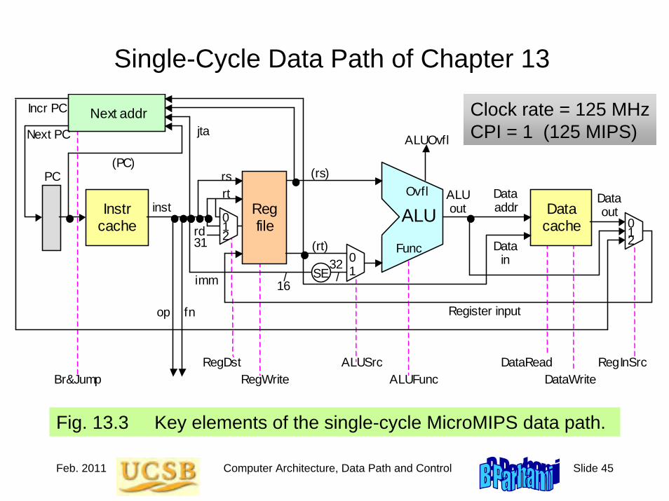
Feb. 2011 Computer Architecture, Data Path and Control Slide 45
Single-Cycle Data Path of Chapter 13
Fig. 13.3 Key elements of the single-cycle MicroMIPS data path.
/
ALU
Data cache
Instr cache
Next addr
Reg file
op
jta
fn
inst
imm
rs (rs)
(rt)
Data addr
Data in 0
1
ALUSrc ALUFunc DataWrite
DataRead
SE
RegInSrc
rt
rd
RegDst RegWrite
32 / 16
Register input
Data out
Func
ALUOvfl
Ovfl
31
0 1 2
Next PC
Incr PC
(PC)
Br&Jump
ALU out
PC
0 1 2
Clock rate = 125 MHzCPI = 1 (125 MIPS)

Feb. 2011 Computer Architecture, Data Path and Control Slide 46
Multicycle Data Path of Chapter 14
Fig. 14.3 Key elements of the multicycle MicroMIPS data path.
Clock rate = 500 MHzCPI ≅ 4 (≅ 125 MIPS)
/
16
rs
0 1
0 1 2
ALU
Cache Reg file
op
jta
fn
(rs)
(rt)
Address
Data
Inst Reg
Data Reg
x Reg
y Reg
z Reg PC
×4
ALUSrcX
ALUFunc
MemWrite MemRead
RegInSrc
4
rd
RegDst RegWrite
/
32
Func
ALUOvfl
Ovfl
31
PCSrc PCWrite IRWrite
ALU out
0 1
0 1
0 1 2 3
0 1 2 3
Inst′Data ALUSrcY
SysCallAddr
/
26
×4
rt
ALUZero
Zero
x Mux
y Mux
0 1
JumpAddr
4 MSBs
/
30
30
SE
imm
2

Feb. 2011 Computer Architecture, Data Path and Control Slide 47
Getting the Best of Both Worlds
Single-cycle:Clock rate = 125 MHz
CPI = 1
Multicycle:Clock rate = 500 MHz
CPI ≅ 4
Pipelined:Clock rate = 500 MHz
CPI ≅ 1
Single-cycle analogy:Doctor appointments scheduled for 60 min per patient
Multicycle analogy:Doctor appointments scheduled in 15-min increments

Feb. 2011 Computer Architecture, Data Path and Control Slide 48
15.1 Pipelining Concepts
Fig. 15.1 Pipelining in the student registration process.
Strategies for improving performance1 – Use multiple independent data paths accepting several instructions
that are read out at once: multiple-instruction-issue or superscalar
2 – Overlap execution of several instructions, starting the next instruction before the previous one has run to completion: (super)pipelined
Approval Cashier Registrar ID photo Pickup
Start here
Exit
1 2 3 4 5 22

Feb. 2011 Computer Architecture, Data Path and Control Slide 49
Pipelined Instruction Execution
Fig. 15.2 Pipelining in the MicroMIPS instruction execution process.
Cycle 7 Cycle 6 Cycle 5 Cycle 4 Cycle 3 Cycle 2 Cycle 1 Cycle 8
Reg file
Reg f ile ALU
Reg file
Reg f ile ALU
Reg file
Reg f ile ALU
Reg f ile
Reg f ile ALU
Reg file
Reg f ile ALU
Cycle 9
Instr cache
Instr cache
Instr cache
Instr cache
Instr cache
Data cache
Data cache
Data cache
Data cache
Data cache
Time dimension
Task dimension
Ins
tr 1
Ins
tr 2
Ins
tr 3
Ins
tr 4
Ins
tr 5

Feb. 2011 Computer Architecture, Data Path and Control Slide 50
Alternate Representations of a Pipeline
Fig. 15.3 Two abstract graphical representations of a 5-stage pipeline executing 7 tasks (instructions).
1
2
3
4
5
1
2
3
4
5
6
7
(a) Task-time diagram (b) Space-time diagram
Cycle
Instruction
Cycle
Pipeline stage
1 2 3 4 5 6 7 8 9 10 11 1 2 3 4 5 6 7 8 9 10 11
Start-up region
Drainageregion
a
a
a
a
a
a
a
w
w
w
w
w
w
w
f
f
f
f
f
f
f
r
r
r
r
r
r
r
d
d
d
d
d
d
d
a a a a a a a
w w w w w w w
d d d d d d d
r r r r r r r
f f f f f f f
f = Fetch r = Reg read a = ALU op d = Data access w = Writeback
Except for start-up and drainage overheads, a pipeline can execute one instruction per clock tick; IPS is dictated by the clock frequency

Feb. 2011 Computer Architecture, Data Path and Control Slide 51
Pipelining Example in a PhotocopierExample 15.1
A photocopier with an x-sheet document feeder copies the first sheet in 4 s and each subsequent sheet in 1 s. The copier’s paper path is a 4-stage pipeline with each stage having a latency of 1s. The firstsheet goes through all 4 pipeline stages and emerges after 4 s. Each subsequent sheet emerges 1s after the previous sheet. How does the throughput of this photocopier vary with x, assuming that loading the document feeder and removing the copies takes 15 s.
Solution
Each batch of x sheets is copied in 15 + 4 + (x – 1) = 18 + x seconds. A nonpipelined copier would require 4x seconds to copy x sheets. For x > 6, the pipelined version has a performance edge. When x = 50, the pipelining speedup is (4 × 50) / (18 + 50) = 2.94.

Feb. 2011 Computer Architecture, Data Path and Control Slide 52
15.2 Pipeline Stalls or Bubbles
Fig. 15.4 Read-after-write data dependency and its possible resolution through data forwarding .
Cycle 7 Cycle 6 Cycle 5 Cycle 4 Cycle 3 Cycle 2 Cycle 1 Cycle 8
Reg f ile
Reg f ile ALU
Reg file
Reg file ALU
Reg f ile
Reg file ALU
Reg f ile
Reg f ile ALU
$5 = $6 + $7
$8 = $8 + $6
$9 = $8 + $2
sw $9, 0($3)
Data forwarding
Instr cache
Instr cache
Instr cache
Instr cache
Data cache
Data cache
Data cache
Data cache
First type of data dependency

Feb. 2011 Computer Architecture, Data Path and Control Slide 53
Inserting Bubbles in a Pipeline
Without data forwarding, three bubbles are needed to resolve a read-after-write data dependency
Cycle 7 Cycle 6 Cycle 5 Cycle 4 Cycle 3 Cycle 2 Cycle 1 Cycle 8
Reg f ile
Reg file ALU
Reg f ile
Reg f ile ALU
Reg file
Reg f ile ALU
Reg file
Reg f ile ALU
Reg f ile
Reg f ile ALU
Cycle 9
Instr cache
Instr cache
Instr cache
Instr cache
Instr cache
Data cache
Data cache
Data cache
Data cache
Data cache
Time dimension
Task dimension
Ins
tr 1
Ins
tr 2
Ins
tr 3
Ins
tr 4
Ins
tr 5
Bubble
Bubble
Bubble
Writes into $8
Reads from $8
Cycle 7 Cycle 6 Cycle 5 Cycle 4 Cycle 3 Cycle 2 Cycle 1 Cycle 8
Reg f ile
Reg file ALU
Reg f ile
Reg f ile ALU
Reg file
Reg f ile ALU
Reg file
Reg f ile ALU
Reg f ile
Reg f ile ALU
Cycle 9
Instr cache
Instr cache
Instr cache
Instr cache
Instr cache
Data cache
Data cache
Data cache
Data cache
Data cache
Time dimension
Task dimension
Ins
tr 1
Ins
tr 2
Ins
tr 3
Ins
tr 4
Ins
tr 5
Bubble
Bubble
Writes into $8
Reads from $8
Two bubbles, if we assume that a register can be updated and read from in one cycle
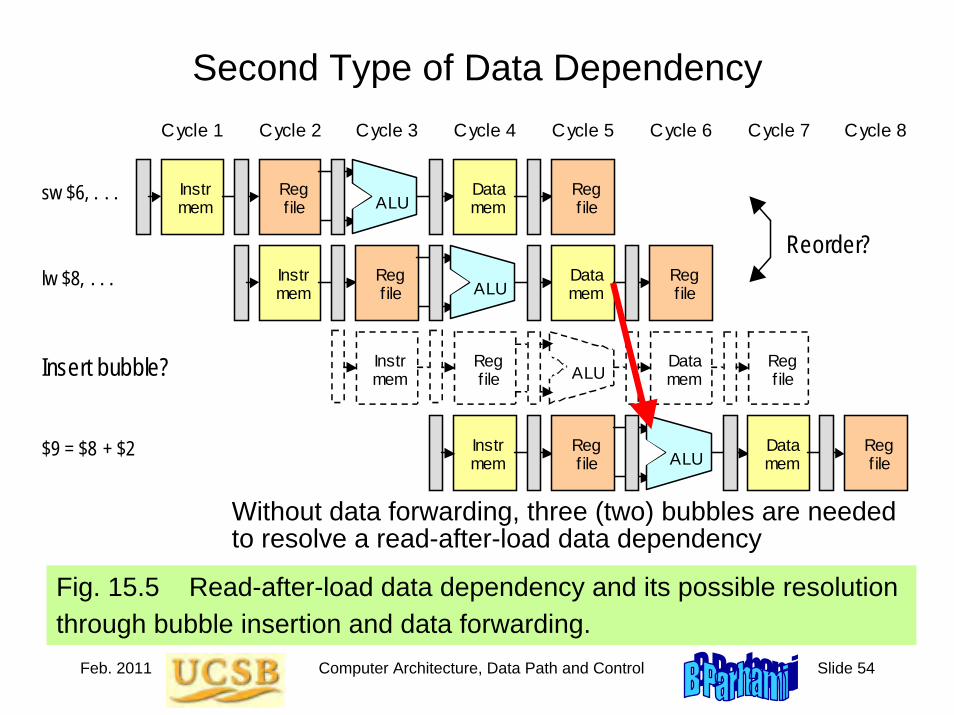
Feb. 2011 Computer Architecture, Data Path and Control Slide 54
Second Type of Data Dependency
Fig. 15.5 Read-after-load data dependency and its possible resolution through bubble insertion and data forwarding.
Cycle 7 Cycle 6 Cycle 5 Cycle 4 Cycle 3 Cycle 2 Cycle 1 Cycle 8
Data mem
Instr mem
Reg file
Reg f ile ALU
Data mem
Instr mem
Reg f ile
Reg f ile ALU
Data mem
Instr mem
Reg f ile
Reg f ile ALU
sw $6, . . .
lw $8, . . .
Insert bubble?
$9 = $8 + $2
Data mem
Instr mem
Reg file
Reg f ile ALU
Reorder?
Without data forwarding, three (two) bubbles are needed to resolve a read-after-load data dependency

Feb. 2011 Computer Architecture, Data Path and Control Slide 55
Control Dependency in a Pipeline
Fig. 15.6 Control dependency due to conditional branch.
Cycle 7 Cycle 6 Cycle 5 Cycle 4 Cycle 3 Cycle 2 Cycle 1 Cycle 8
Data mem
Instr mem
Reg f ile
Reg f ile ALU
Data mem
Instr mem
Reg file
Reg file ALU
Data mem
Instr mem
Reg f ile
Reg file ALU
$6 = $3 + $5
beq $1, $2, . . .
Insert bubble?
$9 = $8 + $2
Data mem
Instr mem
Reg f ile
Reg f ile ALU
Reorder? (delayed branch)
Assume branch resolved here
Here would need 1-2 more bubbles

Feb. 2011 Computer Architecture, Data Path and Control Slide 56
15.3 Pipeline Timing and Performance
Fig. 15.7 Pipelined form of a function unit with latching overhead.
τ
Stage 1
Stage 2
Stage 3
Stage q − 1
Stage q
t/q
Function unit
t
. . .
Latching of results
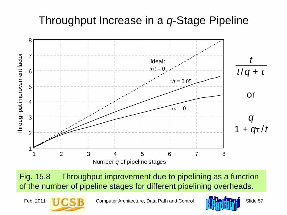
Feb. 2011 Computer Architecture, Data Path and Control Slide 57
Fig. 15.8 Throughput improvement due to pipelining as a function of the number of pipeline stages for different pipelining overheads.
Throughput Increase in a q-Stage Pipeline
1 2 3 4 5 6 7 8 Number q of pipeline stages
Thro
ughp
ut im
prov
emen
t fac
tor
1
2
3
4
5
6
7
8
Ideal: τ/t = 0
τ/t = 0.1
τ/t = 0.05
tt /q + τ
or
q1 + qτ / t
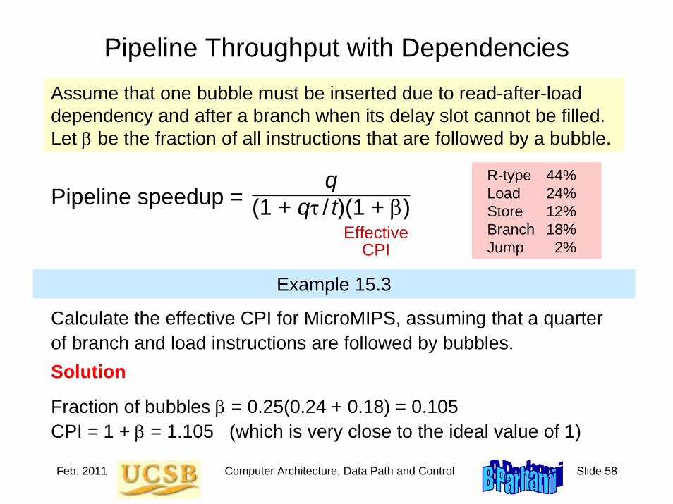
Feb. 2011 Computer Architecture, Data Path and Control Slide 58
Assume that one bubble must be inserted due to read-after-load dependency and after a branch when its delay slot cannot be filled.Let β be the fraction of all instructions that are followed by a bubble.
Pipeline Throughput with Dependencies
q(1 + qτ / t)(1 + β)Pipeline speedup =
R-type 44%Load 24%Store 12%Branch 18%Jump 2%
Example 15.3
Calculate the effective CPI for MicroMIPS, assuming that a quarter of branch and load instructions are followed by bubbles.Solution
Fraction of bubbles β = 0.25(0.24 + 0.18) = 0.105CPI = 1 + β = 1.105 (which is very close to the ideal value of 1)
EffectiveCPI

Feb. 2011 Computer Architecture, Data Path and Control Slide 59
15.4 Pipelined Data Path Design
Fig. 15.9 Key elements of the pipelined MicroMIPS data path. ALU
Data
cache Instr
cache
Next addr
Reg file
op fn
inst
imm
rs (rs)
(rt)
Data addr
ALUSrc ALUFunc DataWrite DataRead
RegInSrc
rt
rd
RegDst RegWrite
Func
ALUOvfl
Ovfl
IncrPC
Br&Jump
PC
1 Incr
0 1
rt
31
0 1 2
NextPC
0 1
SeqInst
0 1 2
0 1
RetAddr
Stage 1 Stage 2 Stage 3 Stage 4 Stage 5
SE
Address
Data

Feb. 2011 Computer Architecture, Data Path and Control Slide 60
15.5 Pipelined Control
Fig. 15.10 Pipelined control signals. ALU
Data
cache Instr
cache
Next addr
Reg file
op fn
inst
imm
rs (rs)
(rt)
Data addr
ALUSrc ALUFunc
DataWrite DataRead
RegInSrc
rt
rd
RegDst RegWrite
Func
ALUOvfl
Ovfl
IncrPC
Br&Jump
PC
1 Incr
0 1
rt
31
0 1 2
NextPC
0 1
SeqInst
0 1 2
0 1
RetAddr
Stage 1 Stage 2 Stage 3 Stage 4 Stage 5
SE
5 3
2
Address
Data

Feb. 2011 Computer Architecture, Data Path and Control Slide 61
15.6 Optimal Pipelining
Fig. 15.11 Higher-throughput pipelined data path for MicroMIPS and the execution of consecutive instructions in it .
Data cache
Instr cache
Data cache
Instr cache
Data cache
Instr cache
Reg f ile
Reg file ALU
Reg file
Reg f ile ALU
Reg f ile
Reg file ALU
Instruction fetch
Register readout
ALU operation
Data read/store
Register writeback
PC
MicroMIPS pipeline with more than four-fold improvement
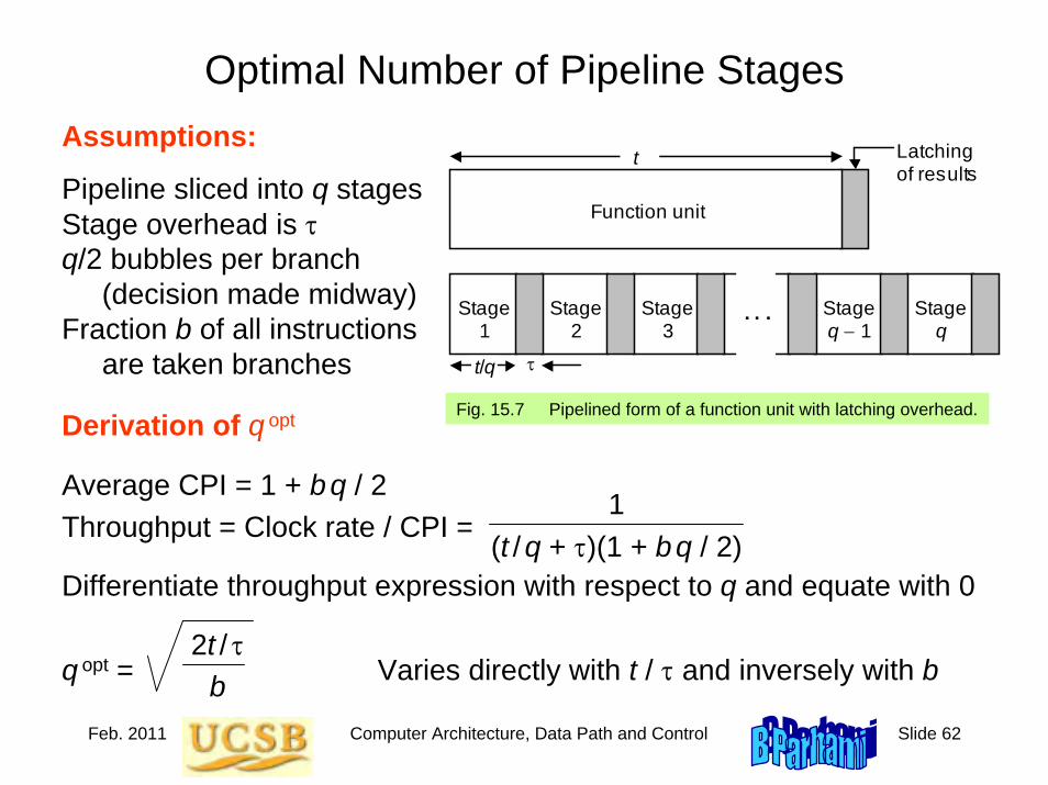
Feb. 2011 Computer Architecture, Data Path and Control Slide 62
Optimal Number of Pipeline Stages
Fig. 15.7 Pipelined form of a function unit with latching overhead.
τ
Stage 1
Stage 2
Stage 3
Stage q − 1
Stage q
t/q
Function unit
t
. . .
Latching of results
Derivation of q opt
Average CPI = 1 + bq / 2Throughput = Clock rate / CPI =
Differentiate throughput expression with respect to q and equate with 0
q opt = Varies directly with t / τ and inversely with b
Assumptions:
Pipeline sliced into q stagesStage overhead is τq/2 bubbles per branch
(decision made midway)Fraction b of all instructions
are taken branches
2t / τb
1(t /q + τ)(1 + bq / 2)

Feb. 2011 Computer Architecture, Data Path and Control Slide 63
Pipeline register placement, Option 2
Pipelining ExampleAn example combinational-logic data path to compute z := (u + v)(w – x) / y
Add/Sub latency
2 ns
Multiply latency
6 ns
Divide latency15 ns
Throughput, original = 1/(25 × 10–9)= 40 M computations / s
×
/
+
−
y
u
v
w
xz
Readout, 1 ns
Write, 1 ns
Throughput, option 1 = 1/(17 × 10–9)= 58.8 M computations / s
Throughput, Option 2 = 1/(10 × 10–9)= 100 M computations / sPipeline register
placement, Option 1
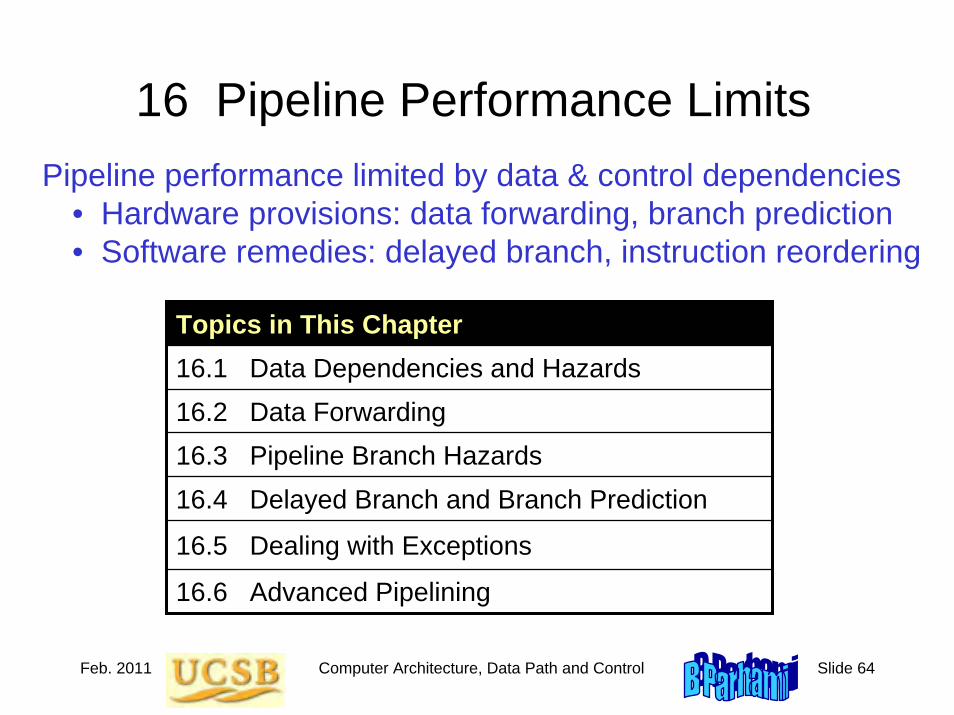
Feb. 2011 Computer Architecture, Data Path and Control Slide 64
16 Pipeline Performance LimitsPipeline performance limited by data & control dependencies
• Hardware provisions: data forwarding, branch prediction• Software remedies: delayed branch, instruction reordering
Topics in This Chapter16.1 Data Dependencies and Hazards16.2 Data Forwarding16.3 Pipeline Branch Hazards16.4 Delayed Branch and Branch Prediction
16.5 Dealing with Exceptions
16.6 Advanced Pipelining
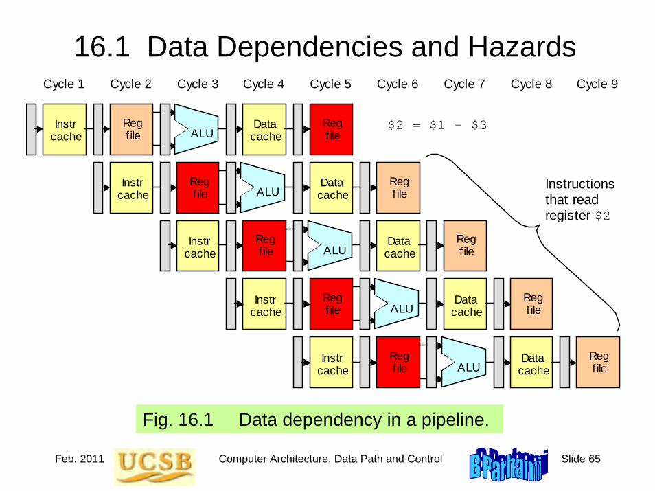
Feb. 2011 Computer Architecture, Data Path and Control Slide 65
16.1 Data Dependencies and Hazards
Fig. 16.1 Data dependency in a pipeline.
Cycle 7 Cycle 6 Cycle 5 Cycle 4 Cycle 3 Cycle 2 Cycle 1 Cycle 8
Reg file
Reg f ile ALU
Reg f ile
Reg f ile ALU
Reg file
Reg f ile ALU
Reg file
Reg f ile ALU
Reg f ile
Reg f ile ALU
Cycle 9
$2 = $1 - $3
Instructions that read register $2
Instr cache
Instr cache
Instr cache
Instr cache
Instr cache
Data cache
Data cache
Data cache
Data cache
Data cache
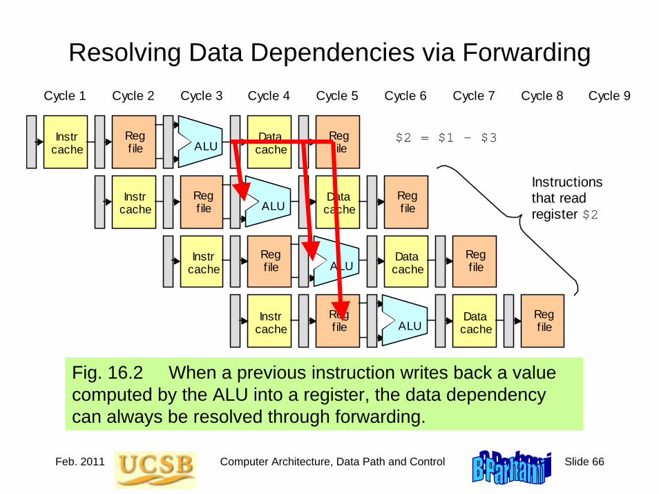
Feb. 2011 Computer Architecture, Data Path and Control Slide 66
Fig. 16.2 When a previous instruction writes back a value computed by the ALU into a register, the data dependency can always be resolved through forwarding.
Cycle 7 Cycle 6 Cycle 5 Cycle 4 Cycle 3 Cycle 2 Cycle 1 Cycle 8
Resolving Data Dependencies via Forwarding
Reg f ile
Reg f ile ALU
Reg f ile
Reg f ile ALU
Reg file
Reg file ALU
Reg f ile
Reg file ALU
Cycle 9
$2 = $1 - $3
Instructions that read register $2
Instr cache
Instr cache
Instr cache
Instr cache
Data cache
Data cache
Data cache
Data cache

Feb. 2011 Computer Architecture, Data Path and Control Slide 67
Pipelined MicroMIPS – Repeated for Reference
Fig. 15.10 Pipelined control signals. ALU
Data
cache Instr
cache
Next addr
Reg file
op fn
inst
imm
rs (rs)
(rt)
Data addr
ALUSrc ALUFunc
DataWrite DataRead
RegInSrc
rt
rd
RegDst RegWrite
Func
ALUOvfl
Ovfl
IncrPC
Br&Jump
PC
1 Incr
0 1
rt
31
0 1 2
NextPC
0 1
SeqInst
0 1 2
0 1
RetAddr
Stage 1 Stage 2 Stage 3 Stage 4 Stage 5
SE
5 3
2
Address
Data

Feb. 2011 Computer Architecture, Data Path and Control Slide 68
Fig. 16.3 When the immediately preceding instruction writes a value read out from the data memory into a register, the data dependency cannot be resolved through forwarding (i.e., we cannot go back in time) and a bubble must be inserted in the pipeline.
Cycle 7 Cycle 6 Cycle 5 Cycle 4 Cycle 3 Cycle 2 Cycle 1 Cycle 8
Certain Data Dependencies Lead to Bubbles
Reg f ile
Reg f ile ALU
Reg f ile
Reg f ile ALU
Reg file
Reg file ALU
Reg f ile
Reg file ALU
Cycle 9
lw $2,4($12)
Instructions that read register $2
Instr cache
Instr cache
Instr cache
Instr cache
Data cache
Data cache
Data cache
Data cache
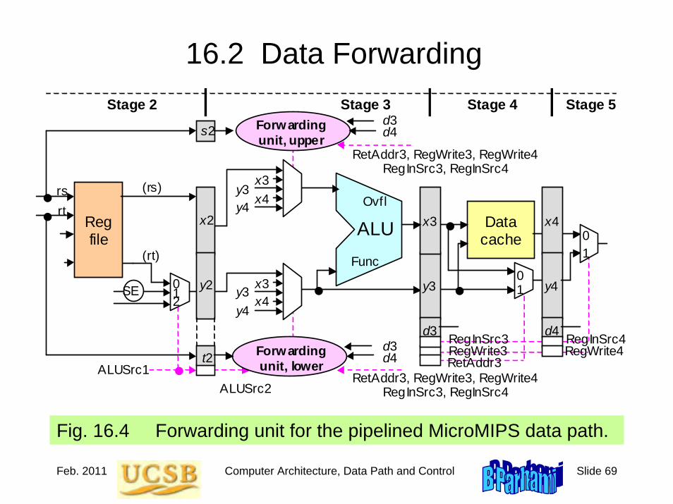
Feb. 2011 Computer Architecture, Data Path and Control Slide 69
16.2 Data Forwarding
Fig. 16.4 Forwarding unit for the pipelined MicroMIPS data path.
(rt)
0 1 2
SE
ALU
Data cache
RegInSrc4
Func
Ovfl
0 1
0 1
RegWrite4 RetAddr3
(rs)
ALUSrc1
Stage 3 Stage 4 Stage 5 Stage 2
x3
y3
x4
y4 x3 y3 x4
y4
RegWrite3 d3 d4
x3 y3
x4 y4
Reg file
rs rt
RegInSrc3
ALUSrc2
s2
t2
d4 d3
RetAddr3, RegWrite3, RegWrite4 RegInSrc3, RegInSrc4
RetAddr3, RegWrite3, RegWrite4 RegInSrc3, RegInSrc4
d4 d3
Forwarding unit, upper
Forwarding unit, lower
x2
y2
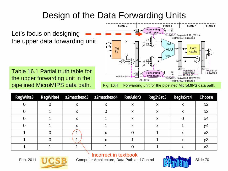
Feb. 2011 Computer Architecture, Data Path and Control Slide 70
Design of the Data Forwarding Units
Fig. 16.4 Forwarding unit for the pipelined MicroMIPS data path.
(rt)
0 1 2
SE
ALU
Data cache
RegInSrc4
Func
Ovfl
0 1
0 1
RegWrite4 RetAddr3
(rs)
ALUSrc1
Stage 3 Stage 4 Stage 5 Stage 2
x3
y3
x4
y4 x3 y3 x4
y4
RegWrite3 d3 d4
x3 y3
x4 y4
Reg file
rs rt
RegInSrc3
ALUSrc2
s2
t2
d4 d3
RetAddr3, RegWrite3, RegWrite4 RegInSrc3, RegInSrc4
RetAddr3, RegWrite3, RegWrite4 RegInSrc3, RegInSrc4
d4 d3
Forwarding unit, upper
Forwarding unit, lower
x2
y2
RegWrite3 RegWrite4 s2matchesd3 s2matchesd4 RetAddr3 RegInSrc3 RegInSrc4 Choose0 0 x x x x x x20 1 x 0 x x x x20 1 x 1 x x 0 x40 1 x 1 x x 1 y41 0 1 x 0 1 x x31 0 1 x 1 1 x y31 1 1 1 0 1 x x3
Table 16.1 Partial truth table for the upper forwarding unit in the pipelined MicroMIPS data path.
Let’s focus on designing the upper data forwarding unit
Incorrect in textbook
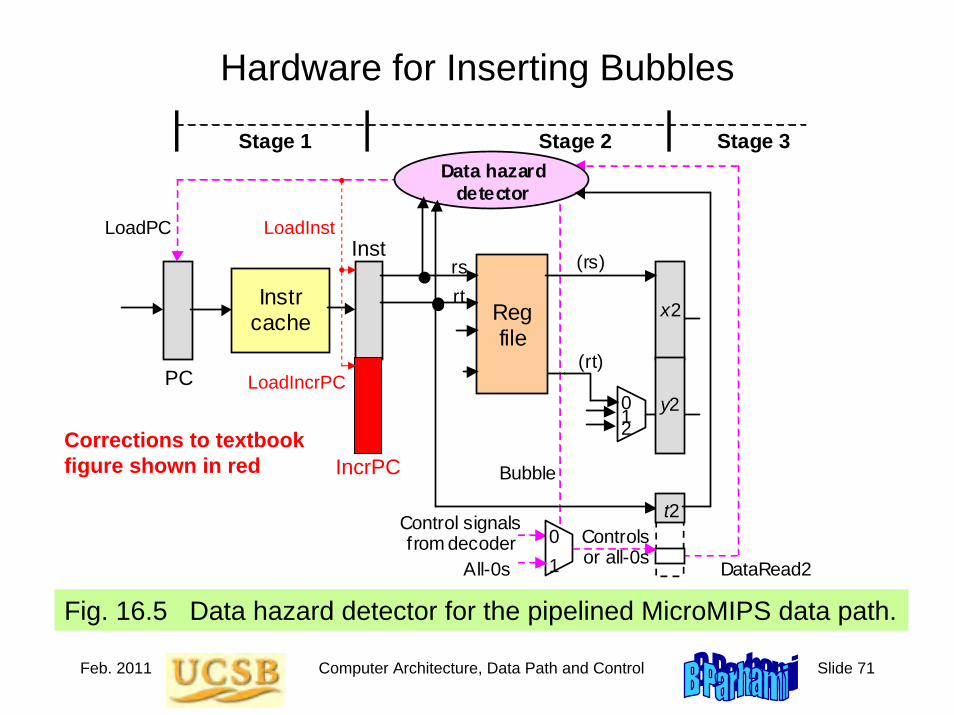
Feb. 2011 Computer Architecture, Data Path and Control Slide 71
Hardware for Inserting Bubbles
Fig. 16.5 Data hazard detector for the pipelined MicroMIPS data path.
(rt)
0 1 2
(rs)
Stage 3 Stage 2
Reg file
rs rt
t2
Data hazard detector
x2
y2
Control signals from decoder
DataRead2
Instr cache
LoadPC
Stage 1
PC Inst reg
All-0s
0 1
Bubble
Controls or all-0s
Inst
IncrPC
LoadInst
LoadIncrPC
Corrections to textbook figure shown in red
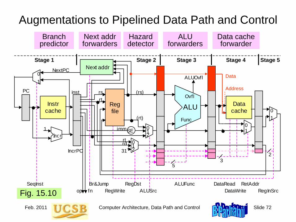
Feb. 2011 Computer Architecture, Data Path and Control Slide 72
Augmentations to Pipelined Data Path and Control
Fig. 15.10 ALU
Data
cache Instr
cache
Next addr
Reg file
op fn
inst
imm
rs (rs)
(rt)
Data addr
ALUSrc ALUFunc
DataWrite DataRead
RegInSrc
rt
rd
RegDst RegWrite
Func
ALUOvfl
Ovfl
IncrPC
Br&Jump
PC
1 Incr
0 1
rt
31
0 1 2
NextPC
0 1
SeqInst
0 1 2
0 1
RetAddr
Stage 1 Stage 2 Stage 3 Stage 4 Stage 5
SE
5 3
2
Address
Data
ALU forwarders
Hazard detector
Data cache forwarder
Next addrforwarders
Branch predictor

Feb. 2011 Computer Architecture, Data Path and Control Slide 73
16.3 Pipeline Branch Hazards
Software-based solutions
Compiler inserts a “no-op” after every branch (simple, but wasteful)
Branch is redefined to take effect after the instruction that follows it
Branch delay slot(s) are filled with useful instructions via reordering
Hardware-based solutions
Mechanism similar to data hazard detector to flush the pipeline
Constitutes a rudimentary form of branch prediction:Always predict that the branch is not taken, flush if mistaken
More elaborate branch prediction strategies possible

Feb. 2011 Computer Architecture, Data Path and Control Slide 74
16.4 Branch PredictionPredicting whether a branch will be taken
• Always predict that the branch will not be taken
• Use program context to decide (backward branch is likely taken, forward branch is likely not taken)
• Allow programmer or compiler to supply clues
• Decide based on past history (maintain a small history table); to be discussed later
• Apply a combination of factors: modern processorsuse elaborate techniques due to deep pipelines

Feb. 2011 Computer Architecture, Data Path and Control Slide 75
Forward and Backward Branches
List A is stored in memory beginning at the address given in $s1. List length is given in $s2. Find the largest integer in the list and copy it into $t0.
Solution
Scan the list, holding the largest element identified thus far in $t0.lw $t0,0($s1) # initialize maximum to A[0]addi $t1,$zero,0 # initialize index i to 0
loop: add $t1,$t1,1 # increment index i by 1beq $t1,$s2,done # if all elements examined, quitadd $t2,$t1,$t1 # compute 2i in $t2add $t2,$t2,$t2 # compute 4i in $t2 add $t2,$t2,$s1 # form address of A[i] in $t2 lw $t3,0($t2) # load value of A[i] into $t3slt $t4,$t0,$t3 # maximum < A[i]?beq $t4,$zero,loop # if not, repeat with no changeaddi $t0,$t3,0 # if so, A[i] is the new maximum j loop # change completed; now repeat
done: ... # continuation of the program
Example 5.5

Feb. 2011 Computer Architecture, Data Path and Control Slide 76
Simple Branch Prediction: 1-Bit History
Two-state branch prediction scheme.
Predicttaken
Predictnot taken
Taken
Not takenNot taken
Taken
Problem with this approach:
Each branch in a loop entails two mispredictions:
Once in first iteration (loop is repeated, but the history indicates exit from loop)
Once in last iteration (when loop is terminated, but history indicates repetition)

Feb. 2011 Computer Architecture, Data Path and Control Slide 77
Simple Branch Prediction: 2-Bit History
Fig. 16.6 Four-state branch prediction scheme.
Not taken
Predict taken
Predict taken again
Predict not taken
Predict not taken
again
Not taken Taken
Not taken Taken
Taken Not taken
Taken
Example 16.1L1: ----
----L2: ----
----br <c2> L2----br <c1> L1
20 iter’s
10 iter’s Impact of different branch prediction schemes
Solution
Always taken: 11 mispredictions, 94.8% accurate1-bit history: 20 mispredictions, 90.5% accurate2-bit history: Same as always taken
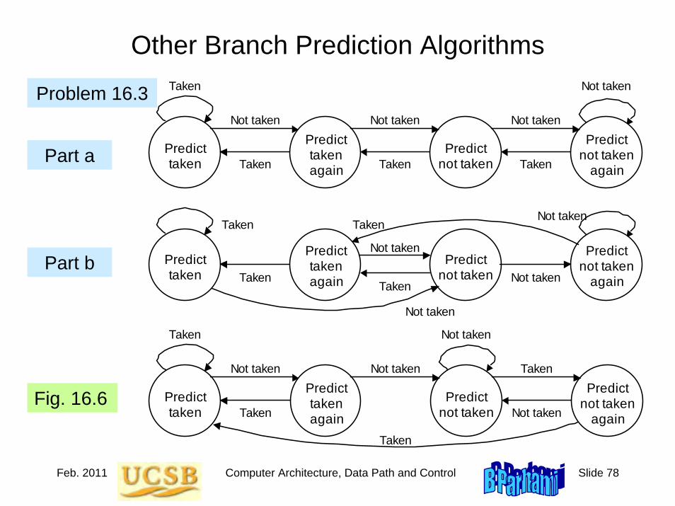
Feb. 2011 Computer Architecture, Data Path and Control Slide 78
Other Branch Prediction Algorithms
Problem 16.3Not taken
Predict taken
Predict taken again
Predict not taken
Predict not taken
again
Not taken
Taken
Not taken
Taken
Taken Not taken
Taken
Not taken
Predict taken
Predict taken again
Predict not taken
Predict not taken
again
Not taken
Taken
Not taken Taken
Taken Not taken
Taken
Not taken
Predict taken
Predict taken again
Predict not taken
Predict not taken
again
Not taken Taken
Not taken Taken
Taken Not taken
Taken
Fig. 16.6
Part a
Part b

Feb. 2011 Computer Architecture, Data Path and Control Slide 79
Hardware Implementation of Branch Prediction
Fig. 16.7 Hardware elements for a branch prediction scheme.
The mapping scheme used to go from PC contents to a table entry is the same as that used in direct-mapped caches (Chapter 18)
Compare
Addresses of recent branch instructions
Target addresses
History bit(s) Low-order
bits used as index
Logic From PC
Incremented PC
Next PC
0
1
=
Read-out table entry

Feb. 2011 Computer Architecture, Data Path and Control Slide 80
Pipeline Augmentations – Repeated for Reference
Fig. 15.10 ALU
Data
cache Instr
cache
Next addr
Reg file
op fn
inst
imm
rs (rs)
(rt)
Data addr
ALUSrc ALUFunc
DataWrite DataRead
RegInSrc
rt
rd
RegDst RegWrite
Func
ALUOvfl
Ovfl
IncrPC
Br&Jump
PC
1 Incr
0 1
rt
31
0 1 2
NextPC
0 1
SeqInst
0 1 2
0 1
RetAddr
Stage 1 Stage 2 Stage 3 Stage 4 Stage 5
SE
5 3
2
Address
Data
ALU forwarders
Hazard detector
Data cache forwarder
Next addrforwarders
Branch predictor
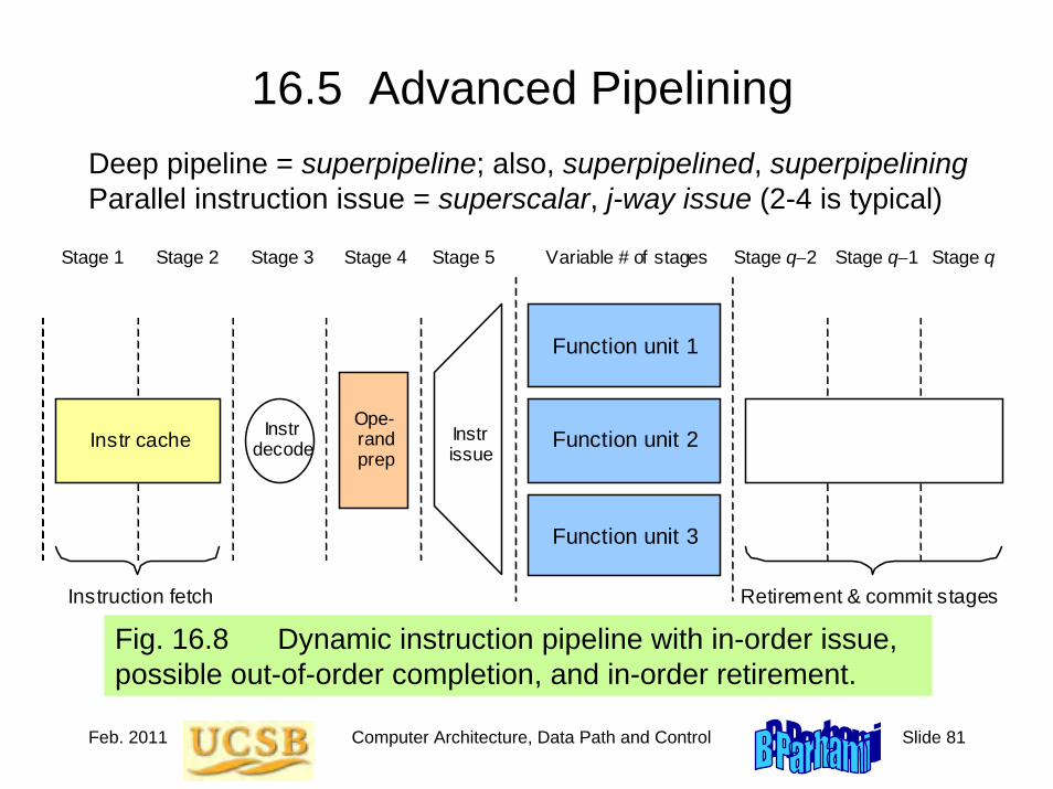
Feb. 2011 Computer Architecture, Data Path and Control Slide 81
16.5 Advanced Pipelining
Fig. 16.8 Dynamic instruction pipeline with in-order issue, possible out-of-order completion, and in-order retirement.
Deep pipeline = superpipeline; also, superpipelined, superpipeliningParallel instruction issue = superscalar, j-way issue (2-4 is typical)
Stage 1
Instr cache
Instruction fetch
Function unit 1
Function unit 2
Function unit 3
Stage 2 Stage 3 Stage 4 Variable # of stages Stage q−2 Stage q−1 Stage q
Ope- rand prep
Instr decode
Retirement & commit stages
Instr issue
Stage 5
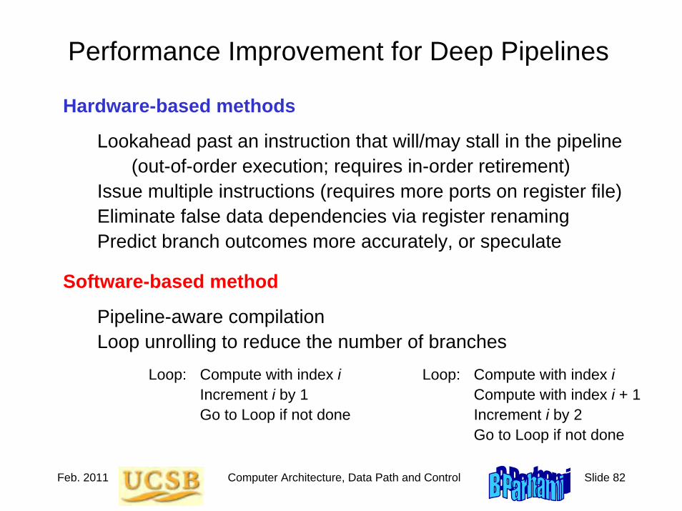
Feb. 2011 Computer Architecture, Data Path and Control Slide 82
Performance Improvement for Deep Pipelines
Hardware-based methods
Lookahead past an instruction that will/may stall in the pipeline(out-of-order execution; requires in-order retirement)
Issue multiple instructions (requires more ports on register file)Eliminate false data dependencies via register renamingPredict branch outcomes more accurately, or speculate
Software-based method
Pipeline-aware compilationLoop unrolling to reduce the number of branches
Loop: Compute with index i Loop: Compute with index iIncrement i by 1 Compute with index i + 1Go to Loop if not done Increment i by 2
Go to Loop if not done

Feb. 2011 Computer Architecture, Data Path and Control Slide 83
CPI Variations with Architectural Features
Table 16.2 Effect of processor architecture, branch prediction methods, and speculative execution on CPI.
Architecture Methods used in practice CPINonpipelined, multicycle Strict in-order instruction issue and exec 5-10
Nonpipelined, overlapped In-order issue, with multiple function units 3-5
Pipelined, static In-order exec, simple branch prediction 2-3
Superpipelined, dynamic Out-of-order exec, adv branch prediction 1-2
Superscalar 2- to 4-way issue, interlock & speculation 0.5-1
Advanced superscalar 4- to 8-way issue, aggressive speculation 0.2-0.5
3.3 inst / cycle × 3 Gigacycles / s ≅ 10 GIPS
Need 100 for TIPS performanceNeed 100,000 for 1 PIPS

Feb. 2011 Computer Architecture, Data Path and Control Slide 84
Development of Intel’s Desktop/Laptop Micros
In the beginning, there was the 8080; led to the 80x86 = IA32 ISA
Half a dozen or so pipeline stages
802868038680486Pentium (80586)
A dozen or so pipeline stages, with out-of-order instruction execution
Pentium ProPentium IIPentium IIICeleron
Two dozens or so pipeline stages
Pentium 4
More advanced technology
More advanced technology
Instructions are broken into micro-ops which are executed out-of-order but retired in-order

Feb. 2011 Computer Architecture, Data Path and Control Slide 85
Current State of Computer Performance
Multi-GIPS/GFLOPS desktops and laptops
Very few users need even greater computing powerUsers unwilling to upgrade just to get a faster processorCurrent emphasis on power reduction and ease of use
Multi-TIPS/TFLOPS in large computer centers
World’s top 500 supercomputers, http://www.top500.orgNext list due in June 2009; as of Nov. 2008:All 500 >> 10 TFLOPS, ≈30 > 100 TFLOPS, 1 > PFLOPS
Multi-PIPS/PFLOPS supercomputers on the drawing board
IBM “smarter planet” TV commercial proclaims (in early 2009):“We just broke the petaflop [sic] barrier.”The technical term “petaflops” is now in the public sphere

Feb. 2011 Computer Architecture, Data Path and Control Slide 86
The Shrinking Supercomputer

Feb. 2011 Computer Architecture, Data Path and Control Slide 87
16.6 Dealing with ExceptionsExceptions present the same problems as branches
How to handle instructions that are ahead in the pipeline?(let them run to completion and retirement of their results)
What to do with instructions after the exception point?(flush them out so that they do not affect the state)
Precise versus imprecise exceptions
Precise exceptions hide the effects of pipelining and parallelism by forcing the same state as that of strict sequential execution
(desirable, because exception handling is not complicated)
Imprecise exceptions are messy, but lead to faster hardware(interrupt handler can clean up to offer precise exception)

Feb. 2011 Computer Architecture, Data Path and Control Slide 88
The Three Hardware Designs for MicroMIPS
/
ALU
Data cache
Instr cache
Next addr
Reg file
op
jta
fn
inst
imm
rs (rs)
(rt)
Data addr
Data in 0
1
ALUSrc ALUFunc DataWrite
DataRead
SE
RegInSrc
rt
rd
RegDst RegWrite
32 / 16
Register input
Data out
Func
ALUOvfl
Ovfl
31
0 1 2
Next PC
Incr PC
(PC)
Br&Jump
ALU out
PC
0 1 2
Single-cycle
/
16
rs
0 1
0 1 2
ALU
Cache Reg file
op
jta
fn
(rs)
(rt)
Address
Data
Inst Reg
Data Reg
x Reg
y Reg
z Reg PC
×4
ALUSrcX
ALUFunc
MemWrite MemRead
RegInSrc
4
rd
RegDst RegWrite
/
32
Func
ALUOvfl
Ovf l
31
PCSrc PCWrite IRWrite
ALU out
0 1
0 1
0 1 2 3
0 1 2 3
Inst′Data ALUSrcY
SysCallAddr
/
26
×4
rt
ALUZero
Zero
x Mux
y Mux
0 1
JumpAddr
4 MSBs
/
30
30
SE
imm
Multicycle
125 MHzCPI = 1
500 MHzCPI ≅ 1.1
500 MHzCPI ≅ 4
ALU
Data cache
Instr cache
Next addr
Reg file
op fn
inst
imm
rs (rs)
(rt)
Data addr
ALUSrc A LUFunc
DataWrite DataRead
Reg InSrc
rt
rd
RegDst RegWrite
Func
ALUOvf l
Ovf l
IncrPC
Br&Jump
PC
1 Incr
0 1
rt
31
0 1 2
NextPC
0 1
SeqInst
0 1 2
0 1
RetAddr
Stage 1 Stage 2 Stage 3 Stage 4 Stage 5
SE
5 3
2
Address
Data
Feb. 2011 Computer Architecture, Data Path and Control Slide 89
Where Do We Go from Here?
Memory Design: How to build a memory unitthat responds in 1 clock
Input and Output:Peripheral devices, I/O programming,interfacing, interrupts
Higher Performance:Vector/array processingParallel processing

Feb. 2011 Computer Architecture, Memory System Design Slide 1
Part VMemory System Design

Feb. 2011 Computer Architecture, Memory System Design Slide 2
About This PresentationThis presentation is intended to support the use of the textbookComputer Architecture: From Microprocessors to Supercomputers, Oxford University Press, 2005, ISBN 0-19-515455-X. It is updated regularly by the author as part of his teaching of the upper-division course ECE 154, Introduction to Computer Architecture, at the University of California, Santa Barbara. Instructors can use these slides freely in classroom teaching and for other educational purposes. Any other use is strictly prohibited. © Behrooz Parhami
Edition Released Revised Revised Revised RevisedFirst July 2003 July 2004 July 2005 Mar. 2006 Mar. 2007
Mar. 2008 Feb. 2009 Feb. 2011

Feb. 2011 Computer Architecture, Memory System Design Slide 3
V Memory System Design
Topics in This PartChapter 17 Main Memory ConceptsChapter 18 Cache Memory OrganizationChapter 19 Mass Memory ConceptsChapter 20 Virtual Memory and Paging
Design problem – We want a memory unit that:• Can keep up with the CPU’s processing speed• Has enough capacity for programs and data• Is inexpensive, reliable, and energy-efficient

Feb. 2011 Computer Architecture, Memory System Design Slide 4
17 Main Memory ConceptsTechnologies & organizations for computer’s main memory
• SRAM (cache), DRAM (main), and flash (nonvolatile)• Interleaving & pipelining to get around “memory wall”
Topics in This Chapter17.1 Memory Structure and SRAM
17.2 DRAM and Refresh Cycles
17.3 Hitting the Memory Wall
17.4 Interleaved and Pipelined Memory
17.5 Nonvolatile Memory
17.6 The Need for a Memory Hierarchy
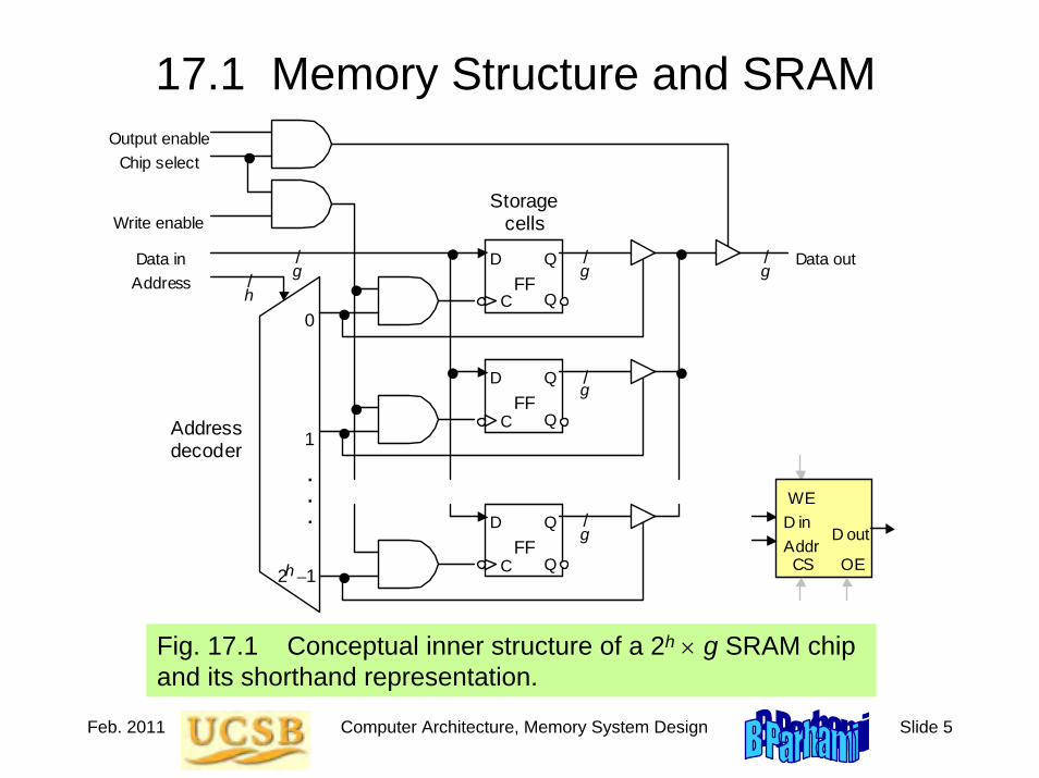
Feb. 2011 Computer Architecture, Memory System Design Slide 5
17.1 Memory Structure and SRAM
Fig. 17.1 Conceptual inner structure of a 2h × g SRAM chip and its shorthand representation.
/ h
Write enable / g
Data in Address
Data out
Chip select
Q
C
Q
D
FF
Q C
Q
D
FF
Q C
Q
D
FF
/ g
Output enable
1
0
2 –1 h
Address decoder
Storage cells
/
g
/ g
/ g
WE
CS
OE
D in D out
Addr
.
.
.

Feb. 2011 Computer Architecture, Memory System Design Slide 6
Multiple-Chip SRAM
Fig. 17.2 Eight 128K × 8 SRAM chips forming a 256K × 32 memory unit.
/
WE
CS
OE
D in D out
Addr
WE
CS
OE
D in D out
Addr
WE
CS
OE
D in D out
Addr
WE
CS
OE
D in D out
Addr
WE
CS
OE
D in D out
Addr
WE
CS
OE
D in D out
Addr
WE
CS
OE
D in D out
Addr
18
/
17
32 WE
CS
OE
D in D out
Addr
Data in
Data out, byte 3
Data out, byte 2
Data out, byte 1
Data out, byte 0
MSB
Address

Feb. 2011 Computer Architecture, Memory System Design Slide 7
SRAM with Bidirectional Data Bus
Fig. 17.3 When data input and output of an SRAM chip are shared or connected to a bidirectional data bus, output must be disabled during write operations.
/ h
/ g
Write enable
Data in/out
Chip select Output enable
Address Data in Data out
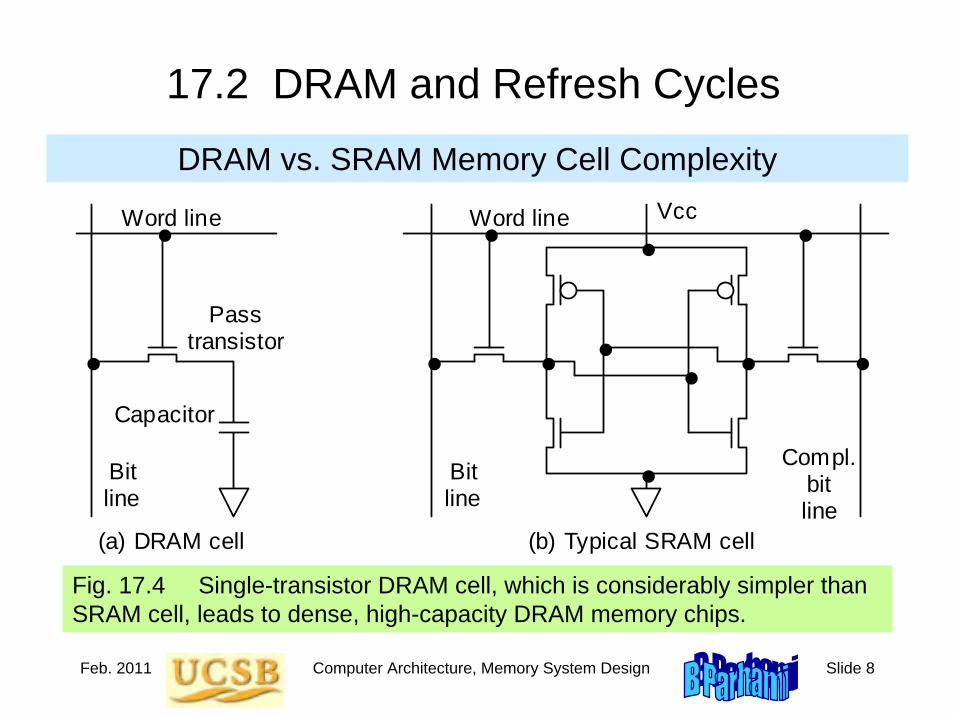
Feb. 2011 Computer Architecture, Memory System Design Slide 8
17.2 DRAM and Refresh Cycles
DRAM vs. SRAM Memory Cell Complexity
Word line
Capacitor
Bit line
Pass transistor
Word line
Bit line
Compl. bit line
Vcc
(a) DRAM cell (b) Typical SRAM cell
Fig. 17.4 Single-transistor DRAM cell, which is considerably simpler than SRAM cell, leads to dense, high-capacity DRAM memory chips.
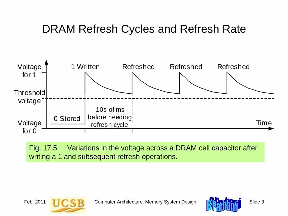
Feb. 2011 Computer Architecture, Memory System Design Slide 9
Fig. 17.5 Variations in the voltage across a DRAM cell capacitor after writing a 1 and subsequent refresh operations.
DRAM Refresh Cycles and Refresh Rate
Time
Threshold voltage
0 Stored
1 Written Refreshed Refreshed Refreshed
10s of ms before needing refresh cycle
Voltage for 1
Voltage for 0

Feb. 2011 Computer Architecture, Memory System Design Slide 10
Loss of Bandwidth to Refresh CyclesExample 17.2
A 256 Mb DRAM chip is organized as a 32M × 8 memory externally and as a 16K × 16K array internally. Rows must be refreshed at least once every 50 ms to forestall data loss; refreshing a row takes 100 ns. What fraction of the total memory bandwidth is lost to refresh cycles?
Column mux
Row
dec
oder
/ h
Address
Square or almost square memory matrix
Row buffer
Row
Column g bits data out
/ g / h
Write enable
/ g
Data in
Address
Data out
Output enable
Chip select
.
.
.
. . .
. . .
(a) SRAM block diagram (b) SRAM read mechanism
Figure 2.10
16K
16K
8
14
11
SolutionRefreshing all 16K rows takes 16 ×1024×100 ns = 1.64 ms. Loss of 1.64 ms every 50 ms amounts to 1.64/50 = 3.3% of the total bandwidth.
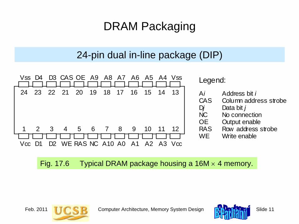
Feb. 2011 Computer Architecture, Memory System Design Slide 11
DRAM Packaging
Fig. 17.6 Typical DRAM package housing a 16M × 4 memory.
Legend:
Ai CAS Dj NC OE RAS WE
1 2 3 4 5 6 7 8 9 10 11 12
24 23 22 21 20 19 18 17 16 15 14 13
A4 A5 A6 A7 A8 A9 D3 D4 CAS OE Vss Vss
A0 A1 A2 A3 A10 D1 D2 RAS WE Vcc Vcc NC
Address bit i Column address strobe Data bit j No connection Output enable Row address strobe Write enable
24-pin dual in-line package (DIP)
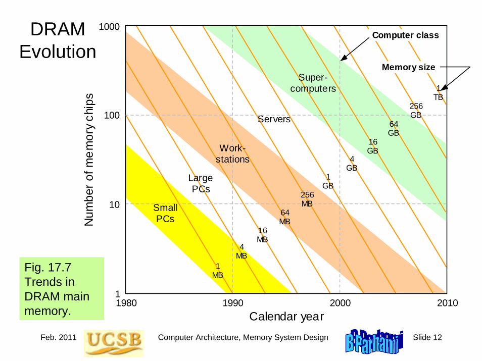
Feb. 2011 Computer Architecture, Memory System Design Slide 12
DRAM Evolution
Fig. 17.7 Trends in DRAM main memory.
1990 1980 2000 2010
Num
ber o
f mem
ory
chip
s
Calendar year
1
10
100
1000
Large PCs
Work- stations
Servers
Super- computers
1 MB
4 MB
16 MB
64 MB
256 MB
1 GB
4 GB
16 GB
64 GB
256 GB
1 TB
Computer class
Memory size
Small PCs
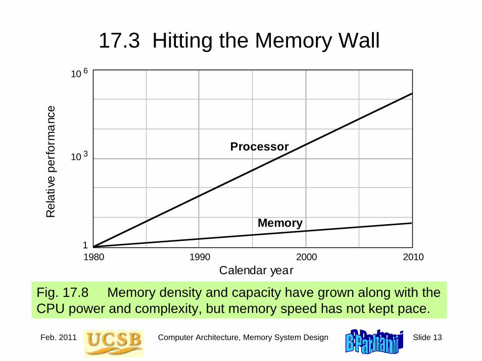
Feb. 2011 Computer Architecture, Memory System Design Slide 13
17.3 Hitting the Memory Wall
Fig. 17.8 Memory density and capacity have grown along with the CPU power and complexity, but memory speed has not kept pace.
1990 1980 2000 20101
10
10
Rel
ativ
e pe
rform
ance
Calendar year
Processor
Memory
3
6

Feb. 2011 Computer Architecture, Memory System Design Slide 14
Bridging the CPU-Memory Speed Gap
Idea: Retrieve more data from memory with each access
Fig. 17.9 Two ways of using a wide-access memory to bridge the speed gap between the processor and memory.
Wide-access
memory
.
.
.
Narrow bus to
processor Mux
Wide-access
memory
. . .
Wide bus to
processor
.
.
. Mux
(a) Buffer and mult iplexer at the memory side
(a) Buffer and mult iplexer at the processor side
. . .

Feb. 2011 Computer Architecture, Memory System Design Slide 15
17.4 Pipelined and Interleaved Memory
Address translation
Row decoding & read out
Column decoding
& selection
Tag comparison & validation
Fig. 17.10 Pipelined cache memory.
Memory latency may involve other supporting operationsbesides the physical access itself
Virtual-to-physical address translation (Chap 20)Tag comparison to determine cache hit/miss (Chap 18)
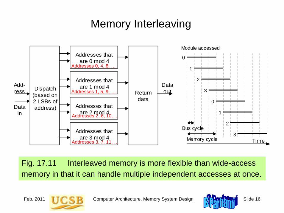
Feb. 2011 Computer Architecture, Memory System Design Slide 16
Memory Interleaving
Fig. 17.11 Interleaved memory is more flexible than wide-access memory in that it can handle multiple independent accesses at once.
Add- ress
Addresses that are 0 mod 4
Addresses that are 2 mod 4
Addresses that are 1 mod 4
Addresses that are 3 mod 4
Return data
Data in
Data out Dispatch
(based on 2 LSBs of address)
Bus cycle
Memory cycle
0
1
2
3
0
1
2
3
Module accessed
Time
Addresses 0, 4, 8, …
Addresses 1, 5, 9, …
Addresses 2, 6, 10, …
Addresses 3, 7, 11, …

Feb. 2011 Computer Architecture, Memory System Design Slide 17
17.5 Nonvolatile Memory
ROM PROM
EPROM
Fig. 17.12 Read-only memory organization, with the fixed contents shown on the right.
B i t l i n e s
Word lines
Word contents
1 0 1 0
1 0 0 1
0 0 1 0
1 1 0 1
S u p p l y v o l t a g e

Feb. 2011 Computer Architecture, Memory System Design Slide 18
Flash Memory
Fig. 17.13 EEPROM or Flash memory organization. Each memory cell is built of a floating-gate MOS transistor.
S o u r c e l i n e s
B i t l i n e s
Word lines
n+
n−
p subs- trate
Control gate
Floating gate
Source
Drain
Feb. 2011 Computer Architecture, Memory System Design Slide 19
17.6 The Need for a Memory Hierarchy
The widening speed gap between CPU and main memory
Processor operations take of the order of 1 ns
Memory access requires 10s or even 100s of ns
Memory bandwidth limits the instruction execution rate
Each instruction executed involves at least one memory access
Hence, a few to 100s of MIPS is the best that can be achieved
A fast buffer memory can help bridge the CPU-memory gap
The fastest memories are expensive and thus not very large
A second (third?) intermediate cache level is thus often used

Feb. 2011 Computer Architecture, Memory System Design Slide 20
Typical Levels in a Hierarchical Memory
Fig. 17.14 Names and key characteristics of levels in a memory hierarchy.
Tertiary Secondary
Main
Cache 2
Cache 1
Reg’s $Millions $100s Ks
$10s Ks
$1000s
$10s
$1s
Cost per GB Access latency Capacity
TBs 10s GB
100s MB
MBs
10s KB
100s B
min+ 10s ms
100s ns
10s ns
a few ns
ns
Speed gap
Feb. 2011 Computer Architecture, Memory System Design Slide 21
Memory Price Trends
Source: https://www1.hitachigst.com/hdd/technolo/overview/chart03.html
$ / G
Byt
e
100K
10K
1K
100
10
1
0.1
Hard disk drive
■ DRAM Flash

Feb. 2011 Computer Architecture, Memory System Design Slide 22
18 Cache Memory OrganizationProcessor speed is improving at a faster rate than memory’s
• Processor-memory speed gap has been widening• Cache is to main as desk drawer is to file cabinet
Topics in This Chapter18.1 The Need for a Cache
18.2 What Makes a Cache Work?
18.3 Direct-Mapped Cache
18.4 Set-Associative Cache
18.5 Cache and Main Memory
18.6 Improving Cache Performance

Feb. 2011 Computer Architecture, Memory System Design Slide 23
18.1 The Need for a Cache
/
ALU
Data cache
Instr cache
Next addr
Reg file
op
jta
fn
inst
imm
rs (rs)
(rt)
Data addr
Data in 0
1
ALUSrc ALUFunc DataWrite
DataRead
SE
RegInSrc
rt
rd
RegDst RegWrite
32 / 16
Register input
Data out
Func
ALUOvfl
Ovfl
31
0 1 2
Next PC
Incr PC
(PC)
Br&Jump
ALU out
PC
0 1 2
Single-cycle
/
16
rs
0 1
0 1 2
ALU
Cache Reg file
op
jta
fn
(rs)
(rt)
Address
Data
Inst Reg
Data Reg
x Reg
y Reg
z Reg PC
×4
ALUSrcX
ALUFunc
MemWrite MemRead
RegInSrc
4
rd
RegDst RegWrite
/
32
Func
ALUOvfl
Ovf l
31
PCSrc PCWrite IRWrite
ALU out
0 1
0 1
0 1 2 3
0 1 2 3
Inst′Data ALUSrcY
SysCallAddr
/
26
×4
rt
ALUZero
Zero
x Mux
y Mux
0 1
JumpAddr
4 MSBs
/
30
30
SE
imm
Multicycle
ALU
Data cache
Instr cache
Next addr
Reg file
op fn
inst
imm
rs (rs)
(rt)
Data addr
ALUSrc ALUFunc
DataWrite DataRead
RegInSrc
rt
rd
RegDst RegWrite
Func
ALUOvfl
Ovfl
IncrPC
Br&Jump
PC
1 Incr
0 1
rt
31
0 1 2
NextPC
0 1
SeqInst
0 1 2
0 1
RetAddr
Stage 1 Stage 2 Stage 3 Stage 4 Stage 5
SE
5 3
2
125 MHzCPI = 1
Pipelined
500 MHzCPI ≅ 4
500 MHzCPI ≅ 1.1
All three of our MicroMIPS designs assumed 2-ns data and instruction memories; however, typical RAMs are 10-50 times slower

Feb. 2011 Computer Architecture, Memory System Design Slide 24
Cache, Hit/Miss Rate, and Effective Access Time
One level of cache with hit rate hCeff = hCfast + (1 – h)(Cslow + Cfast) = Cfast + (1 – h)Cslow
CPU Cache(fast)
memory
Main(slow)
memory
Regfile
WordLine
Data is in the cache fraction h of the time(say, hit rate of 98%)
Go to main 1 – h of the time(say, cache miss rate of 2%)
Cache is transparent to user;transfers occur automatically

Feb. 2011 Computer Architecture, Memory System Design Slide 25
Multiple Cache Levels
Fig. 18.1 Cache memories act as intermediaries between the superfast processor and the much slower main memory.
Level-2 cache
Main memory
CPU CPU registers
Level-1 cache
Level-2 cache
Main memory
CPU CPU registers
Level-1 cache
(a) Level 2 between level 1 and main (b) Level 2 connected to “backside” bus
Cleaner and easier to analyze
Feb. 2011 Computer Architecture, Memory System Design Slide 26
Performance of a Two-Level Cache SystemExample 18.1
A system with L1 and L2 caches has a CPI of 1.2 with no cache miss. There are 1.1 memory accesses on average per instruction. What is the effective CPI with cache misses factored in? What are the effective hit rate and miss penalty overall if L1 and L2 caches are modeled as a single cache?Level Local hit rate Miss penaltyL1 95 % 8 cyclesL2 80 % 60 cycles
Level-2 cache
Main memory
CPU CPU registers
Level-1 cache 8
cycles60
cycles
95% 4%1%
Solution
Ceff = Cfast + (1 – h1)[Cmedium + (1 – h2)Cslow]Because Cfast is included in the CPI of 1.2, we must account for the restCPI = 1.2 + 1.1(1 – 0.95)[8 + (1 – 0.8)60] = 1.2 + 1.1×0.05×20 = 2.3Overall: hit rate 99% (95% + 80% of 5%), miss penalty 60 cycles

Feb. 2011 Computer Architecture, Memory System Design Slide 27
Cache Memory Design ParametersCache size (in bytes or words). A larger cache can hold more of the program’s useful data but is more costly and likely to be slower.
Block or cache-line size (unit of data transfer between cache and main). With a larger cache line, more data is brought in cache with each miss. This can improve the hit rate but also may bring low-utility data in.
Placement policy. Determining where an incoming cache line is stored. More flexible policies imply higher hardware cost and may or may not have performance benefits (due to more complex data location).
Replacement policy. Determining which of several existing cache blocks (into which a new cache line can be mapped) should be overwritten. Typical policies: choosing a random or the least recently used block.
Write policy. Determining if updates to cache words are immediately forwarded to main (write-through) or modified blocks are copied back to main if and when they must be replaced (write-back or copy-back).

Feb. 2011 Computer Architecture, Memory System Design Slide 28
18.2 What Makes a Cache Work?
Fig. 18.2 Assuming no conflict in address mapping, the cache will hold a small program loop in its entirety, leading to fast execution.
9-instruction program loop
Address mapping (many-to-one)
Cache memory
Main memory
Cache l ine/block (unit of t rans fer between main and cache memories)
Temporal localitySpatial locality

Feb. 2011 Computer Architecture, Memory System Design Slide 29
Desktop, Drawer, and File Cabinet Analogy
Fig. 18.3 Items on a desktop (register) or in a drawer (cache) are more readily accessible than those in a file cabinet (main memory).
Main memory
Register file
Access cabinet in 30 s
Access desktop in 2 s
Access drawer in 5 s
Cache memory
Once the “working set” is in the drawer, very few trips to the file cabinet are needed.
Feb. 2011 Computer Architecture, Memory System Design Slide 30
Temporal and Spatial LocalitiesAddresses
Time
From Peter Denning’s CACM paper, July 2005 (Vol. 48, No. 7, pp. 19-24)
Temporal:Accesses to the same address are typically clustered in time
Spatial:When a location is accessed, nearby locations tend to be accessed also
Working set

Feb. 2011 Computer Architecture, Memory System Design Slide 31
Caching Benefits Related to Amdahl’s LawExample 18.2
In the drawer & file cabinet analogy, assume a hit rate h in the drawer. Formulate the situation shown in Fig. 18.2 in terms of Amdahl’s law.
Solution
Without the drawer, a document is accessed in 30 s. So, fetching 1000 documents, say, would take 30 000 s. The drawer causes a fraction hof the cases to be done 6 times as fast, with access time unchanged for the remaining 1 – h. Speedup is thus 1/(1 – h + h/6) = 6 / (6 – 5h). Improving the drawer access time can increase the speedup factor but as long as the miss rate remains at 1 – h, the speedup can never exceed 1 / (1 – h). Given h = 0.9, for instance, the speedup is 4, with the upper bound being 10 for an extremely short drawer access time.Note: Some would place everything on their desktop, thinking that this yields even greater speedup. This strategy is not recommended!
3

Feb. 2011 Computer Architecture, Memory System Design Slide 32
Compulsory, Capacity, and Conflict MissesCompulsory misses: With on-demand fetching, first access to any item is a miss. Some “compulsory” misses can be avoided by prefetching.
Capacity misses: We have to oust some items to make room for others. This leads to misses that are not incurred with an infinitely large cache.
Conflict misses: Occasionally, there is free room, or space occupied by useless data, but the mapping/placement scheme forces us to displace useful items to bring in other items. This may lead to misses in future.
Given a fixed-size cache, dictated, e.g., by cost factors or availability of space on the processor chip, compulsory and capacity misses are pretty much fixed. Conflict misses, on the other hand, are influenced by the data mapping scheme which is under our control.
We study two popular mapping schemes: direct and set-associative.
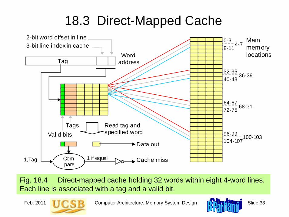
Feb. 2011 Computer Architecture, Memory System Design Slide 33
18.3 Direct-Mapped Cache
Fig. 18.4 Direct-mapped cache holding 32 words within eight 4-word lines. Each line is associated with a tag and a valid bit.
3-bit line index in cache 2-bit word offset in line Main
memory locations
0-3 4-7
8-11
36-39 32-35 40-43
68-71 64-67 72-75
100-103 96-99 104-107
Tag Word
address
Valid bits
Tags
Read tag and specified word
Com-pare
1,Tag
Data out
Cache miss
1 if equal
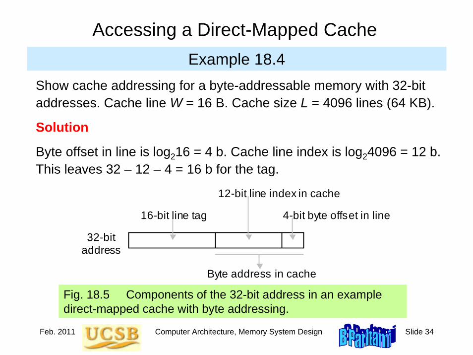
Feb. 2011 Computer Architecture, Memory System Design Slide 34
Accessing a Direct-Mapped CacheExample 18.4
Fig. 18.5 Components of the 32-bit address in an example direct-mapped cache with byte addressing.
12-bit line index in cache
4-bit byte offset in line
Show cache addressing for a byte-addressable memory with 32-bit addresses. Cache line W = 16 B. Cache size L = 4096 lines (64 KB).
Solution
Byte offset in line is log216 = 4 b. Cache line index is log24096 = 12 b.This leaves 32 – 12 – 4 = 16 b for the tag.
Byte address in cache
16-bit line tag
32-bit address

Feb. 2011 Computer Architecture, Memory System Design Slide 35
3-bit line index in cache 2-bit word offset in line
Tag Word
address
Valid bits
Tags
Read tag and specified word
Com-pare
1,Tag
Dat
Cac 1 if equal
Direct-Mapped Cache Behavior
Fig. 18.4
1: miss, line 3, 2, 1, 0 fetched7: miss, line 7, 6, 5, 4 fetched6: hit5: hit
32: miss, line 35,34, 33, 32 fetched (replaces 3, 2, 1, 0)
33: hit1: miss, line 3, 2, 1, 0 fetched
(replaces 35, 34, 33, 32)2: hit
... and so on
1 03 25 47 6
33 3235 34 1 03 2
Address trace:1, 7, 6, 5, 32, 33, 1, 2, . . .

Feb. 2011 Computer Architecture, Memory System Design Slide 36
18.4 Set-Associative Cache
Fig. 18.6 Two-way set-associative cache holding 32 words of data within 4-word lines and 2-line sets.
Main memory locations
0-3
16-19
32-35
48-51
64-67
80-83
96-99
112-115
Valid bits Tags
1
0
2-bit set index in cache
2-bit word offset in line
Tag
Word address
Option 0
Option 1
Read tag and specified word from each option
Com-pare
1,Tag
Com-pare
Data out
Cache
miss
1 if equal

Feb. 2011 Computer Architecture, Memory System Design Slide 37
Accessing a Set-Associative CacheExample 18.5
Fig. 18.7 Components of the 32-bit address in an example two-way set-associative cache.
Show cache addressing scheme for a byte-addressable memory with 32-bit addresses. Cache line width 2W = 16 B. Set size 2S = 2 lines. Cache size 2L = 4096 lines (64 KB).
Solution
Byte offset in line is log216 = 4 b. Cache set index is (log24096/2) = 11 b.This leaves 32 – 11 – 4 = 17 b for the tag.
11-bit set index in cache
4-bit byte offset in line
Address in cache used to read out two candidate
items and their control info
17-bit line tag
32-bit address
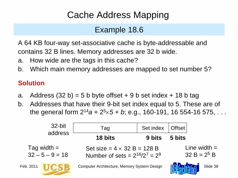
Feb. 2011 Computer Architecture, Memory System Design Slide 38
Cache Address MappingExample 18.6
A 64 KB four-way set-associative cache is byte-addressable and contains 32 B lines. Memory addresses are 32 b wide.a. How wide are the tags in this cache?b. Which main memory addresses are mapped to set number 5?
Solution
a. Address (32 b) = 5 b byte offset + 9 b set index + 18 b tagb. Addresses that have their 9-bit set index equal to 5. These are of
the general form 214a + 25×5 + b; e.g., 160-191, 16 554-16 575, . . .
Tag Set index Offset
18 bits 9 bits 5 bits
32-bitaddress
Line width =32 B = 25 B
Set size = 4 × 32 B = 128 BNumber of sets = 216/27 = 29
Tag width = 32 – 5 – 9 = 18

Feb. 2011 Computer Architecture, Memory System Design Slide 39
18.5 Cache and Main Memory
The writing problem:Write-through slows down the cache to allow main to catch up
Write-back or copy-back is less problematic, but still hurts performance due to two main memory accesses in some cases.
Solution: Provide write buffers for the cache so that it does not have to wait for main memory to catch up.
Harvard architecture: separate instruction and data memoriesvon Neumann architecture: one memory for instructions and data
Split cache: separate instruction and data caches (L1)Unified cache: holds instructions and data (L1, L2, L3)

Feb. 2011 Computer Architecture, Memory System Design Slide 40
Faster Main-Cache Data Transfers
Fig. 18.8 A 256 Mb DRAM chip organized as a 32M × 8 memory module: four such chips could form a 128 MB main memory unit.
16Kb × 16Kb memory matrix
Selected row
Column mux
Row address decoder
16 Kb = 2 KB 14 / 11
/ Byte
address in
Data byte out
. . .
. . .
. . .

Feb. 2011 Computer Architecture, Memory System Design Slide 41
18.6 Improving Cache PerformanceFor a given cache size, the following design issues and tradeoffs exist:
Line width (2W). Too small a value for W causes a lot of main memory accesses; too large a value increases the miss penalty and may tie up cache space with low-utility items that are replaced before being used.
Set size or associativity (2S). Direct mapping (S = 0) is simple and fast; greater associativity leads to more complexity, and thus slower access, but tends to reduce conflict misses. More on this later.
Line replacement policy. Usually LRU (least recently used) algorithm or some approximation thereof; not an issue for direct-mapped caches. Somewhat surprisingly, random selection works quite well in practice.
Write policy. Modern caches are very fast, so that write-through is seldom a good choice. We usually implement write-back or copy-back, using write buffers to soften the impact of main memory latency.

Feb. 2011 Computer Architecture, Memory System Design Slide 42
Effect of Associativity on Cache Performance
Fig. 18.9 Performance improvement of caches with increased associativity.
4-way Direct 16-way 64-way 0
0.1
0.3
Mis
s ra
te
Associativity
0.2
2-way 8-way 32-way

Feb. 2011 Computer Architecture, Memory System Design Slide 43
19 Mass Memory ConceptsToday’s main memory is huge, but still inadequate for all needs
• Magnetic disks provide extended and back-up storage• Optical disks & disk arrays are other mass storage options
Topics in This Chapter19.1 Disk Memory Basics
19.2 Organizing Data on Disk
19.3 Disk Performance
19.4 Disk Caching
19.5 Disk Arrays and RAID
19.6 Other Types of Mass Memory

Feb. 2011 Computer Architecture, Memory System Design Slide 44
19.1 Disk Memory Basics
Fig. 19.1 Disk memory elements and key terms.
Track 0 Track 1
Track c – 1
Sector
Recording area
Spindle
Direction of rotation
Platter
Read/write head
Actuator
Arm
Track 2
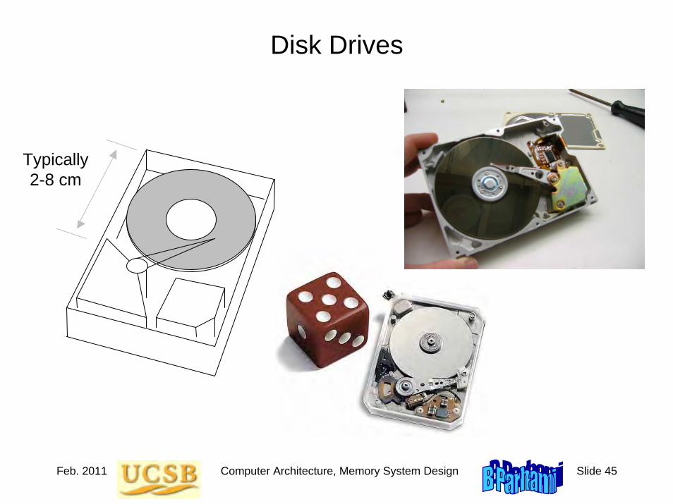
Feb. 2011 Computer Architecture, Memory System Design Slide 45
Disk Drives
Typically
2 - 8 cm
Typically2-8 cm
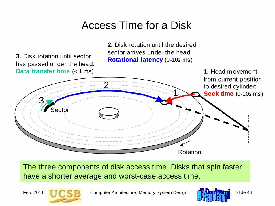
Feb. 2011 Computer Architecture, Memory System Design Slide 46
Access Time for a Disk
The three components of disk access time. Disks that spin fasterhave a shorter average and worst-case access time.
1. Head movement from current position to desired cylinder: Seek time (0-10s ms)
Rotation
2. Disk rotation until the desired sector arrives under the head: Rotational latency (0-10s ms) 3. Disk rotation until sector
has passed under the head: Data transfer time (< 1 ms)
Sector
1 2
3

Feb. 2011 Computer Architecture, Memory System Design Slide 47
Representative Magnetic DisksTable 19.1 Key attributes of three representative magnetic disks, from the highest capacity to the smallest physical size (ca. early 2003). [More detail (weight, dimensions, recording density, etc.) in textbook.]
Manufacturer and Model Name
Seagate Barracuda 180
Hitachi DK23DA
IBM Microdrive
Application domain Server Laptop Pocket deviceCapacity 180 GB 40 GB 1 GBPlatters / Surfaces 12 / 24 2 / 4 1 / 2Cylinders 24 247 33 067 7 167Sectors per track, avg 604 591 140Buffer size 16 MB 2 MB 1/8 MBSeek time, min,avg,max 1, 8, 17 ms 3, 13, 25 ms 1, 12, 19 msDiameter 3.5″ 2.5″ 1.0″Rotation speed, rpm 7 200 4 200 3 600Typical power 14.1 W 2.3 W 0.8 W
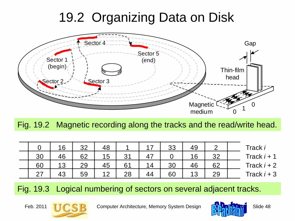
Feb. 2011 Computer Architecture, Memory System Design Slide 48
19.2 Organizing Data on Disk
Fig. 19.2 Magnetic recording along the tracks and the read/write head.
Gap
Thin-film head
0 0 1 Magnetic
medium
Sector 1 (begin)
Sector 4
Sector 5 (end)
Sector 3 Sector 2
Fig. 19.3 Logical numbering of sectors on several adjacent tracks.
0 30 60 27
16 46 13 43
32 62 29 59
48 15 45 12
17 47 14 44
33 0 30 60
49 16 46 13
2 32 62 29
1 31 61 28
Track i Track i + 1 Track i + 2 Track i + 3

Feb. 2011 Computer Architecture, Memory System Design Slide 49
19.3 Disk Performance
Fig. 19.4 Reducing average seek time and rotational latency by performing disk accesses out of order.
Seek time = a + b(c – 1) + β(c – 1)1/2
Average rotational latency = (30 / rpm) s = (30 000 / rpm) ms
Arrival order of access requests: A, B, C, D, E, F Possible out-of-order reading: C, F, D, E, B, A
A
B
C
D
E F
Rotation

Feb. 2011 Computer Architecture, Memory System Design Slide 50
19.4 Disk CachingSame idea as processor cache: bridge main-disk speed gap
Read/write an entire track with each disk access:“Access one sector, get 100s free,” hit rate around 90%
Disks listed in Table 19.1 have buffers from 1/8 to 16 MBRotational latency eliminated; can start from any sectorNeed back-up power so as not to lose changes in disk cache
(need it anyway for head retraction upon power loss)
Placement options for disk cache
In the disk controller:Suffers from bus and controller latencies even for a cache hit
Closer to the CPU:Avoids latencies and allows for better utilization of space
Intermediate or multilevel solutions

Feb. 2011 Computer Architecture, Memory System Design Slide 51
19.5 Disk Arrays and RAID
The need for high-capacity, high-throughput secondary (disk) memory
Processor speed
RAM size
Disk I/O rate
Number of disks
Disk capacity
Number of disks
1 GIPS 1 GB 100 MB/s 1 100 GB 1
1 TIPS 1 TB 100 GB/s 1000 100 TB 100
1 PIPS 1 PB 100 TB/s 1 Million 100 PB 100 000
1 EIPS 1 EB 100 PB/s 1 Billion 100 EB 100 Million
Amdahl’s rules of thumb for system balance
1 RAM bytefor each IPS
100 disk bytesfor each RAM byte
1 I/O bit per secfor each IPS

Feb. 2011 Computer Architecture, Memory System Design Slide 52
Redundant Array of Independent Disks (RAID)
Fig. 19.5 RAID levels 0-6, with a simplified view of data organization.
RAID0: Multiple disks for higher data rate; no redundancy
RAID1: Mirrored disks
RAID2: Error-correcting code
RAID3: Bit- or byte-level striping with parity/checksum disk
RAID4: Parity/checksum applied to sectors,not bits or bytes
RAID5: Parity/checksum distributed across several disks
Data organization on multiple disks
Data disk 0
Data disk 1
Mirror disk 1
Data disk 2
Mirror disk 2
Data disk 0
Data disk 2
Data disk 1
Data disk 3
Mirror disk 0
Parity disk
Spare disk
Spare disk
Data 0 Data 1 Data 2
Data 0’ Data 1’ Data 2’
Data 0” Data 1” Data 2”
Data 0’” Data 1’” Data 2’”
Parity 0 Parity 1 Parity 2
Spare disk
Data 0 Data 1 Data 2
Data 0’ Data 1’ Data 2’
Data 0’” Parity 1 Data 2”
Parity 0 Data 1’” Data 2’”
Data 0” Data 1” Parity 2
RAID6: Parity and 2nd check distributed across several disks
A ⊕ B ⊕ C ⊕ D ⊕ P = 0 →B = A ⊕ C ⊕ D ⊕ P
A B C D P

Feb. 2011 Computer Architecture, Memory System Design Slide 53
RAID Product Examples
IBM ESS Model 750

Feb. 2011 Computer Architecture, Memory System Design Slide 54
19.6 Other Types of Mass Memory
Fig. 3.12 Magnetic and optical disk memory units.
(a) Cutaway view of a hard disk drive (b) Some removable storage media
Typically 2-9 cm
Floppy disk
CD-ROM
Magnetic tape
cartridge
. .
. . . . . .
Flash driveThumb driveTravel drive

Feb. 2011 Computer Architecture, Memory System Design Slide 55
Fig. 19.6 Simplified view of recording format and access mechanism for data on a CD-ROM or DVD-ROM.
Optical Disks
Protective coating Substrate
Pits
Laser diode
Detector
Lenses Side view of
one track
Tracks
Beam splitter
Pits on adjacent
tracks
1 0 1 0 0 1 10
Spiral, rather than concentric, tracks

Feb. 2011 Computer Architecture, Memory System Design Slide 56
Automated Tape Libraries

Feb. 2011 Computer Architecture, Memory System Design Slide 57
20 Virtual Memory and PagingManaging data transfers between main & mass is cumbersome
• Virtual memory automates this process• Key to virtual memory’s success is the same as for cache
Topics in This Chapter
20.1 The Need for Virtual Memory
20.2 Address Translation in Virtual Memory
20.3 Translation Lookaside Buffer
20.4 Page Placement and Replacement
20.5 Main and Mass Memories
20.6 Improving Virtual Memory Performance
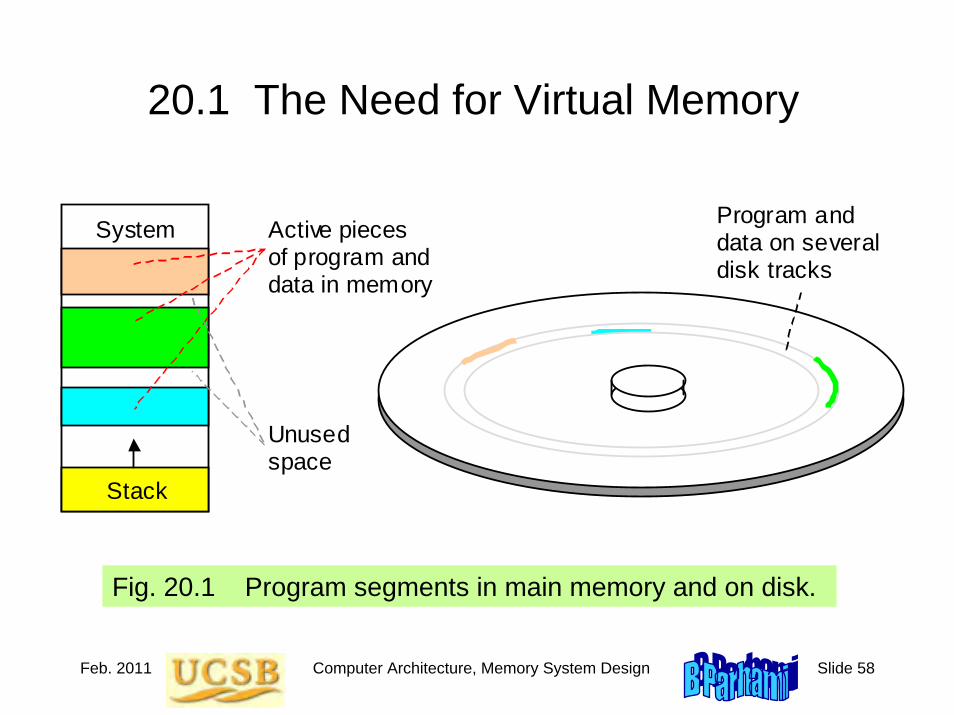
Feb. 2011 Computer Architecture, Memory System Design Slide 58
20.1 The Need for Virtual Memory
Fig. 20.1 Program segments in main memory and on disk.
Program and data on several disk tracks
System
Stack
Active pieces of program and data in memory
Unused space

Feb. 2011 Computer Architecture, Memory System Design Slide 59
Fig. 20.2 Data movement in a memory hierarchy.
Pages Lines
Words
Registers
Main memory
Cache
Memory Hierarchy: The Big Picture
Virtual memory
(transferred explicitly
via load/store) (transferred automatically
upon cache miss) (transferred automatically
upon page fault)
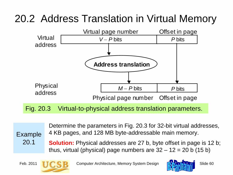
Feb. 2011 Computer Architecture, Memory System Design Slide 60
20.2 Address Translation in Virtual Memory
Fig. 20.3 Virtual-to-physical address translation parameters.
Virtual address
Physical address
Physical page number
Virtual page number Offset in page
Offset in page
Address translation
P bits
P bits
V − P bits
M − P bits
Example 20.1
Determine the parameters in Fig. 20.3 for 32-bit virtual addresses, 4 KB pages, and 128 MB byte-addressable main memory.
Solution: Physical addresses are 27 b, byte offset in page is 12 b; thus, virtual (physical) page numbers are 32 – 12 = 20 b (15 b)

Feb. 2011 Computer Architecture, Memory System Design Slide 61
Page Tables and Address Translation
Fig. 20.4 The role of page table in the virtual-to-physical address translation process.
Page table
Main memory
Valid bits
Page table register
Virtual page
number
Other f lags

Feb. 2011 Computer Architecture, Memory System Design Slide 62
Protection and Sharing in Virtual Memory
Fig. 20.5 Virtual memory as a facilitator of sharing and memory protection.
Page table for process 1
Main memory Permission bits
Pointer Flags
Page table for process 2
To disk memory
Only read accesses allow ed
Read & w rite accesses allowed
01234567
01234567
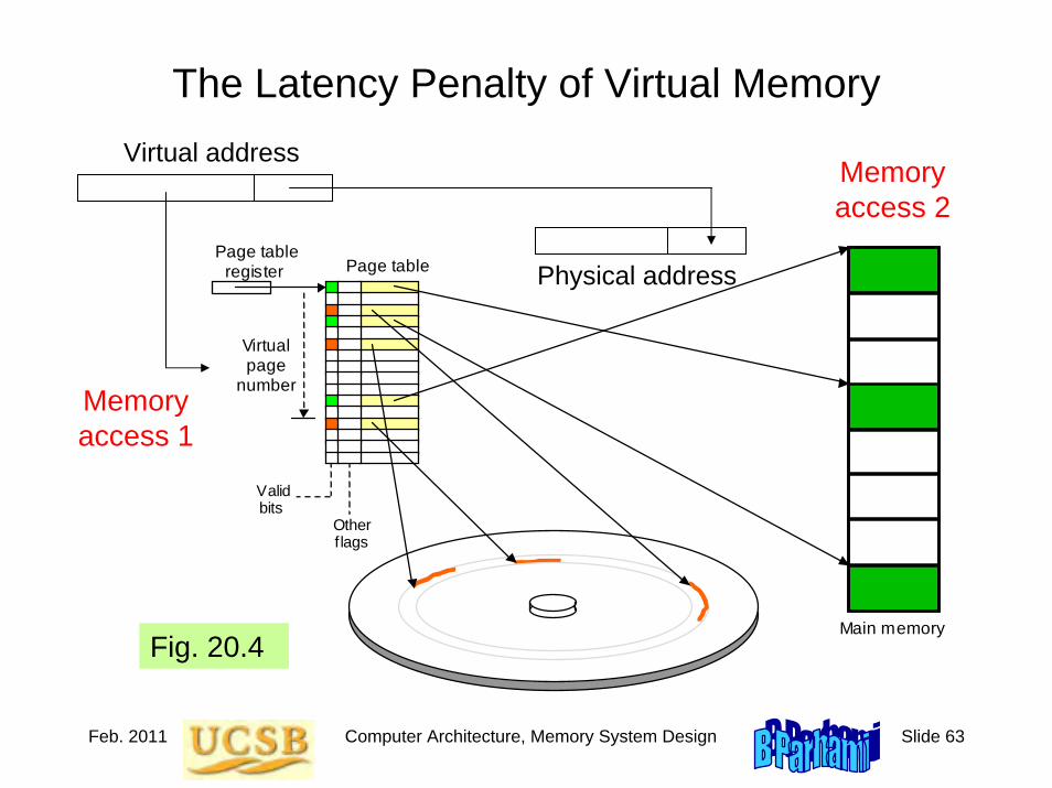
Feb. 2011 Computer Architecture, Memory System Design Slide 63
The Latency Penalty of Virtual Memory
Page table
Main memory
Valid bits
Page table register
Virtual page
number
Other f lags
Virtual address
Memory access 1
Fig. 20.4
Physical address
Memory access 2
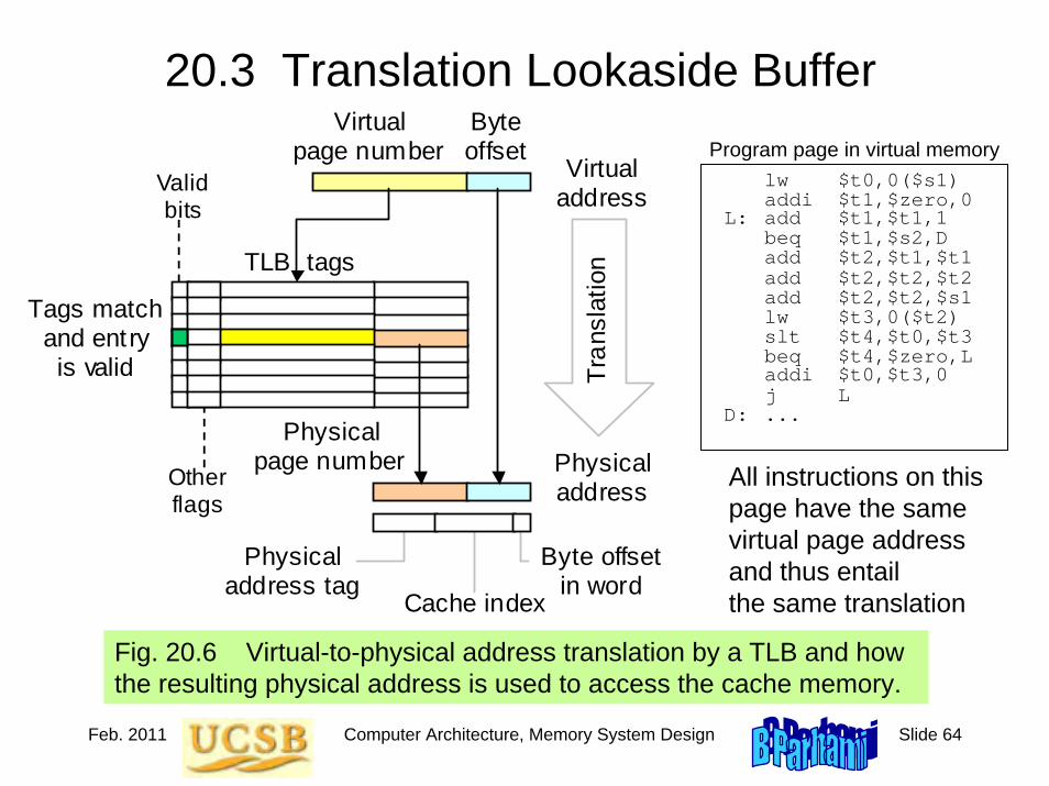
Feb. 2011 Computer Architecture, Memory System Design Slide 64
20.3 Translation Lookaside Buffer
Fig. 20.6 Virtual-to-physical address translation by a TLB and how the resulting physical address is used to access the cache memory.
Virtual page number
Byte offset
Byte offset in word
Physical address tag
Cache index
Valid bits
TLB tags
Tags match and entry is valid
Physical page number Physical
address
Virtual address
Tran
slat
ion
Other flags
lw $t0,0($s1)addi $t1,$zero,0
L: add $t1,$t1,1beq $t1,$s2,Dadd $t2,$t1,$t1add $t2,$t2,$t2add $t2,$t2,$s1lw $t3,0($t2)slt $t4,$t0,$t3beq $t4,$zero,Laddi $t0,$t3,0j L
D: ...
Program page in virtual memory
All instructions on this page have the same virtual page address and thus entail the same translation

Feb. 2011 Computer Architecture, Memory System Design Slide 65
Example 20.2
Address Translation via TLB
An address translation process converts a 32-bit virtual address to a 32-bit physical address. Memory is byte-addressable with 4 KB pages. A 16-entry, direct-mapped TLB is used. Specify the components of the virtual and physical addresses and the width of the various TLB fields.
Solution Virtual page number
Byte offset
Byte offset in word
Physical address tag
Cache index
Valid bits
TLB tags
Tags match and entry is valid
Physical page number Physical
address
Virtual address
Tran
slat
ion
Other flags
12
12
20
20
VirtualPage number
416Tag
16-entryTLB
TLBindex
TLB word width =16-bit tag +20-bit phys page # +1 valid bit +Other flags≥ 37 bits
Fig. 20.6
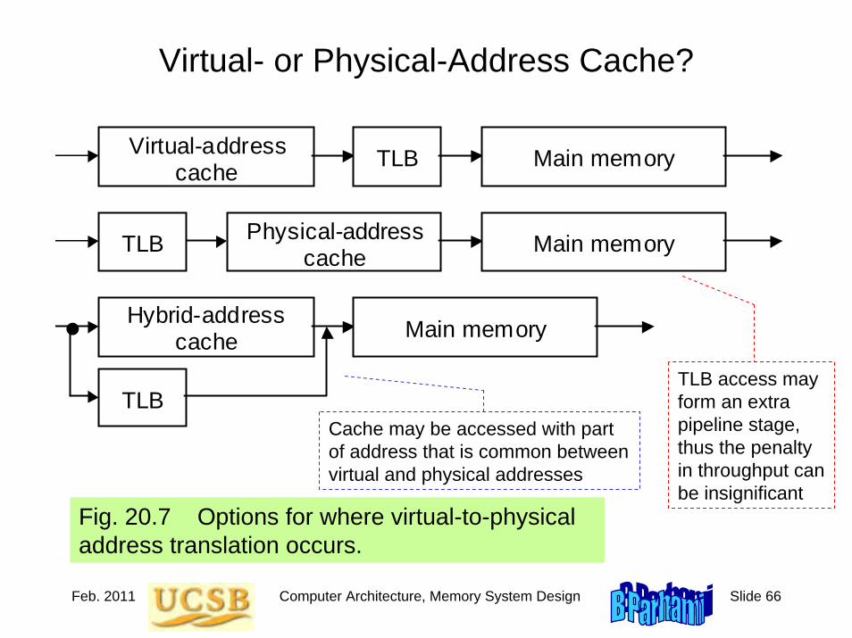
Feb. 2011 Computer Architecture, Memory System Design Slide 66
Virtual- or Physical-Address Cache?
Fig. 20.7 Options for where virtual-to-physical address translation occurs.
TLB Main memory Virtual-address
cache
TLB Main memory Physical-address
cache
TLB
Main memory Hybrid-address cache
TLB access may form an extra pipeline stage, thus the penalty in throughput can be insignificant
Cache may be accessed with part of address that is common between virtual and physical addresses
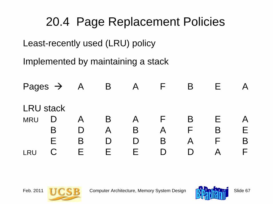
Feb. 2011 Computer Architecture, Memory System Design Slide 67
20.4 Page Replacement Policies
Least-recently used (LRU) policy
Implemented by maintaining a stack
Pages A B A F B E A
LRU stackMRU D A B A F B E A
B D A B A F B EE B D D B A F B
LRU C E E E D D A F

Feb. 2011 Computer Architecture, Memory System Design Slide 68
Approximate LRU Replacement Policy
Fig. 20.8 A scheme for the approximate implementation of LRU .
0
1
0
0
1
1
0
1
0
1
0
1
0
0
0
1
(a) Before replacement (b) After replacement
Page slot 0
Page slot 1Page slot 7
Least-recently used policy: effective, but hard to implement
Approximate versions of LRU are more easily implementedClock policy: diagram below shows the reason for nameUse bit is set to 1 whenever a page is accessed

Feb. 2011 Computer Architecture, Memory System Design Slide 69
LRU Is Not Always the Best PolicyExample 20.2
Computing column averages for a 17 × 1024 table; 16-page memoryfor j = [0 … 1023] {
temp = 0;for i = [0 … 16]
temp = temp + T[i][j]print(temp/17.0); }
Evaluate the page faults for row-major and column-major storage.
Solution
. . .
1024 61 60 60 60 60
17
Fig. 20.9 Pagination of a 17×1024 table with row- or column-major storage.
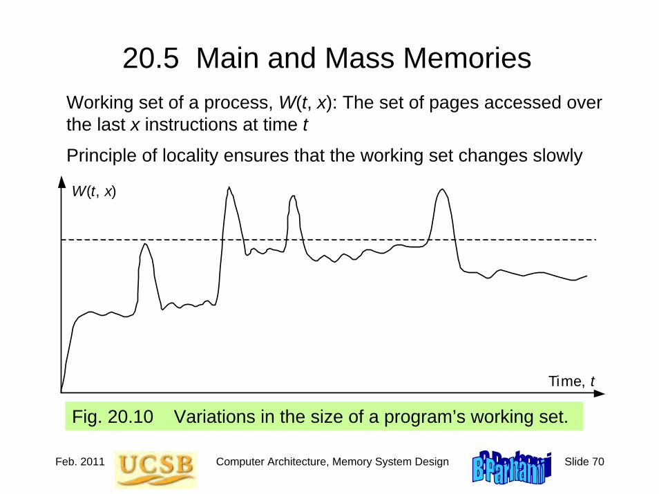
Feb. 2011 Computer Architecture, Memory System Design Slide 70
20.5 Main and Mass Memories
Fig. 20.10 Variations in the size of a program’s working set.
Time, t
W(t, x)
Working set of a process, W(t, x): The set of pages accessed over the last x instructions at time t
Principle of locality ensures that the working set changes slowly

Feb. 2011 Computer Architecture, Memory System Design Slide 71
20.6 Improving Virtual Memory Performance
Table 20.1 Memory hierarchy parameters and their effects on performance
Parameter variation Potential advantages Possible disadvantages
Larger main or cache size
Fewer capacity misses Longer access time
Larger pages or longer lines
Fewer compulsory misses (prefetching effect)
Greater miss penalty
Greater associativity (for cache only)
Fewer conflict misses Longer access time
More sophisticated replacement policy
Fewer conflict misses Longer decision time, more hardware
Write-through policy (for cache only)
No write-back time penalty, easier write-miss handling
Wasted memory bandwidth, longer access time

Feb. 2011 Computer Architecture, Memory System Design Slide 72
Fig. 20.11 Trends in disk, main memory, and CPU speeds.
Impact of Technology on Virtual Memory
1990 1980 2000 2010
Tim
e
Calendar year
Disk seek time
ps
ns
μs
s
ms
CPU cycle time
DRAM access time
Feb. 2011 Computer Architecture, Memory System Design Slide 73
Performance Impact of the Replacement Policy
Fig. 20.12 Dependence of page faults on the number of pages allocated and the page replacement policy
5 0 10 15
Pag
e fa
ult r
ate
Pages allocated
0.00
0.01
0.02
0.04
0.03
Ideal (best possible)
Approximate LRU
Least recently used
First in, first out

Feb. 2011 Computer Architecture, Memory System Design Slide 74
Fig. 20.2 Data movement in a memory hierarchy.
Pages Lines
Words
Registers
Main memory
Cache
Summary of Memory Hierarchy
Virtual memory
(transferred explicitly
via load/store) (transferred automatically
upon cache miss) (transferred automatically
upon page fault)
Cache memory: provides illusion of very high speed
Virtual memory: provides illusion of very large size
Main memory: reasonable cost, but slow & small
Locality makes the illusions work

Feb. 2011 Computer Architecture, Input/Output and Interfacing Slide 1
Part VIInput/Output and Interfacing
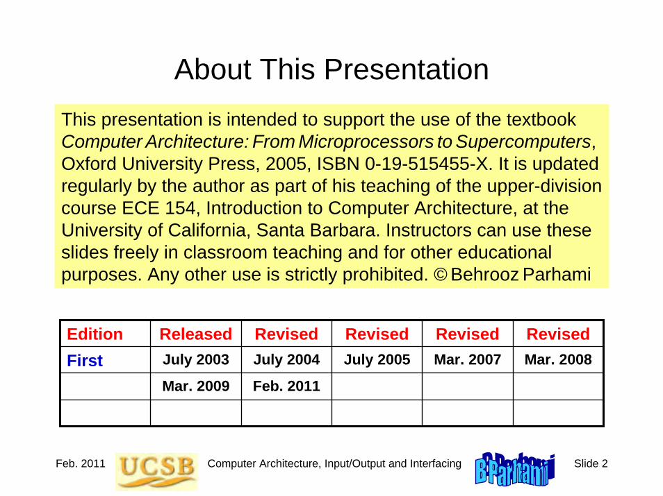
Feb. 2011 Computer Architecture, Input/Output and Interfacing Slide 2
About This PresentationThis presentation is intended to support the use of the textbookComputer Architecture: From Microprocessors to Supercomputers, Oxford University Press, 2005, ISBN 0-19-515455-X. It is updated regularly by the author as part of his teaching of the upper-division course ECE 154, Introduction to Computer Architecture, at the University of California, Santa Barbara. Instructors can use these slides freely in classroom teaching and for other educational purposes. Any other use is strictly prohibited. © Behrooz Parhami
Edition Released Revised Revised Revised RevisedFirst July 2003 July 2004 July 2005 Mar. 2007 Mar. 2008
Mar. 2009 Feb. 2011

Feb. 2011 Computer Architecture, Input/Output and Interfacing Slide 3
VI Input/Output and Interfacing
Topics in This PartChapter 21 Input/Output DevicesChapter 22 Input/Output ProgrammingChapter 23 Buses, Links, and InterfacingChapter 24 Context Switching and Interrupts
Effective computer design & use requires awareness of:• I/O device types, technologies, and performance• Interaction of I/O with memory and CPU• Automatic data collection and device actuation
Feb. 2011 Computer Architecture, Input/Output and Interfacing Slide 4
21 Input/Output DevicesLearn about input and output devices as categorized by:
• Type of data presentation or recording• Data rate, which influences interaction with system
Topics in This Chapter21.1 Input/Output Devices and Controllers
21.2 Keyboard and Mouse
21.3 Visual Display Units
21.4 Hard-Copy Input/Output Devices
21.5 Other Input/Output Devices
21.6 Networking of Input/Output Devices
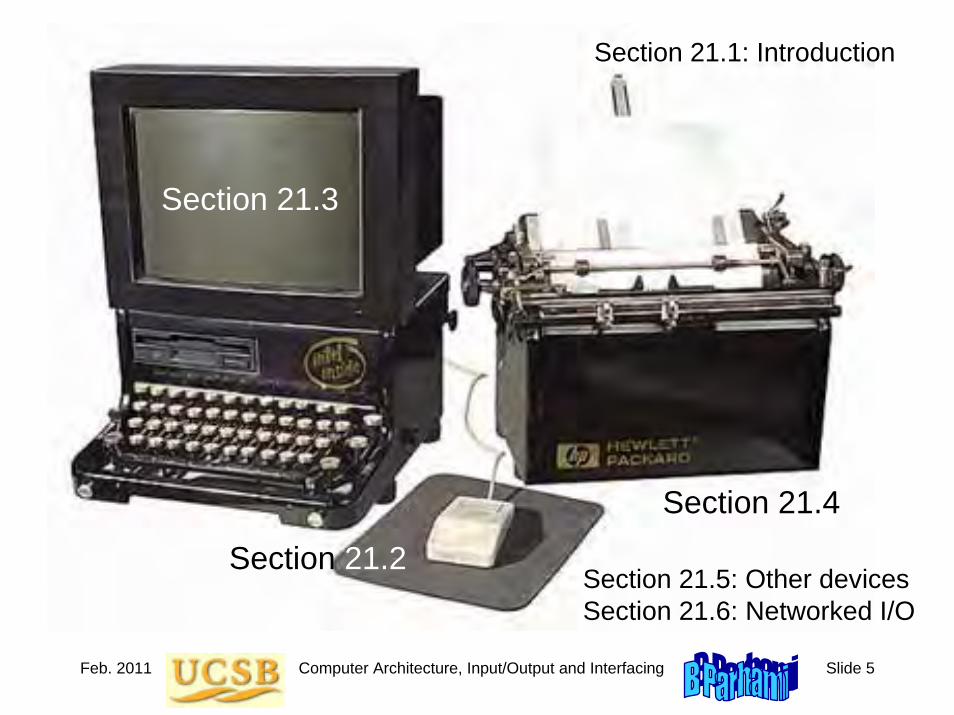
Feb. 2011 Computer Architecture, Input/Output and Interfacing Slide 5
Section 21.2
Section 21.3
Section 21.4
Section 21.1: Introduction
Section 21.5: Other devicesSection 21.6: Networked I/O
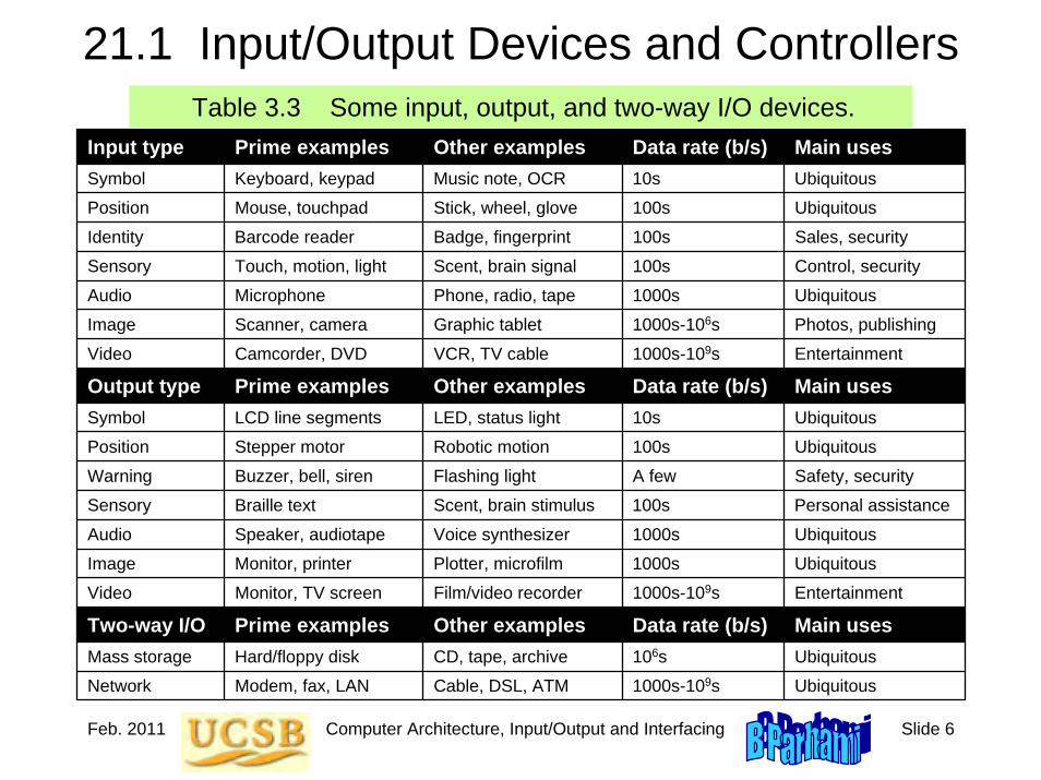
Feb. 2011 Computer Architecture, Input/Output and Interfacing Slide 6
21.1 Input/Output Devices and ControllersTable 3.3 Some input, output, and two-way I/O devices.
Input type Prime examples Other examples Data rate (b/s) Main usesSymbol Keyboard, keypad Music note, OCR 10s Ubiquitous
Position Mouse, touchpad Stick, wheel, glove 100s Ubiquitous
Identity Barcode reader Badge, fingerprint 100s Sales, security
Sensory Touch, motion, light Scent, brain signal 100s Control, security
Audio Microphone Phone, radio, tape 1000s Ubiquitous
Image Scanner, camera Graphic tablet 1000s-106s Photos, publishing
Video Camcorder, DVD VCR, TV cable 1000s-109s Entertainment
Output type Prime examples Other examples Data rate (b/s) Main usesSymbol LCD line segments LED, status light 10s Ubiquitous
Position Stepper motor Robotic motion 100s Ubiquitous
Warning Buzzer, bell, siren Flashing light A few Safety, security
Sensory Braille text Scent, brain stimulus 100s Personal assistance
Audio Speaker, audiotape Voice synthesizer 1000s Ubiquitous
Image Monitor, printer Plotter, microfilm 1000s Ubiquitous
Video Monitor, TV screen Film/video recorder 1000s-109s Entertainment
Two-way I/O Prime examples Other examples Data rate (b/s) Main usesMass storage Hard/floppy disk CD, tape, archive 106s Ubiquitous
Network Modem, fax, LAN Cable, DSL, ATM 1000s-109s Ubiquitous

Feb. 2011 Computer Architecture, Input/Output and Interfacing Slide 7
Simple Organization for Input/Output
Figure 21.1 Input/output via a single common bus.
CPU
Cache
Main memory
I/O controller I/O controller I/O controller
Disk Disk Graphics display Network
System bus
Interrupts
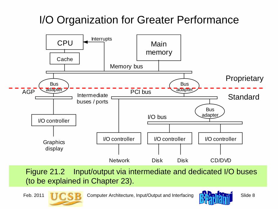
Feb. 2011 Computer Architecture, Input/Output and Interfacing Slide 8
I/O Organization for Greater Performance
Figure 21.2 Input/output via intermediate and dedicated I/O buses (to be explained in Chapter 23).
CPU
Cache
Main memory
I/O controller I/O controller I/O controller
Disk Disk Network CD/DVD
Memory bus
Interrupts
Bus adapter
Bus adapter
Bus adapter
Intermediate buses / ports
I/O bus I/O controller
Graphics display
PCI bus AGP
Proprietary
Standard
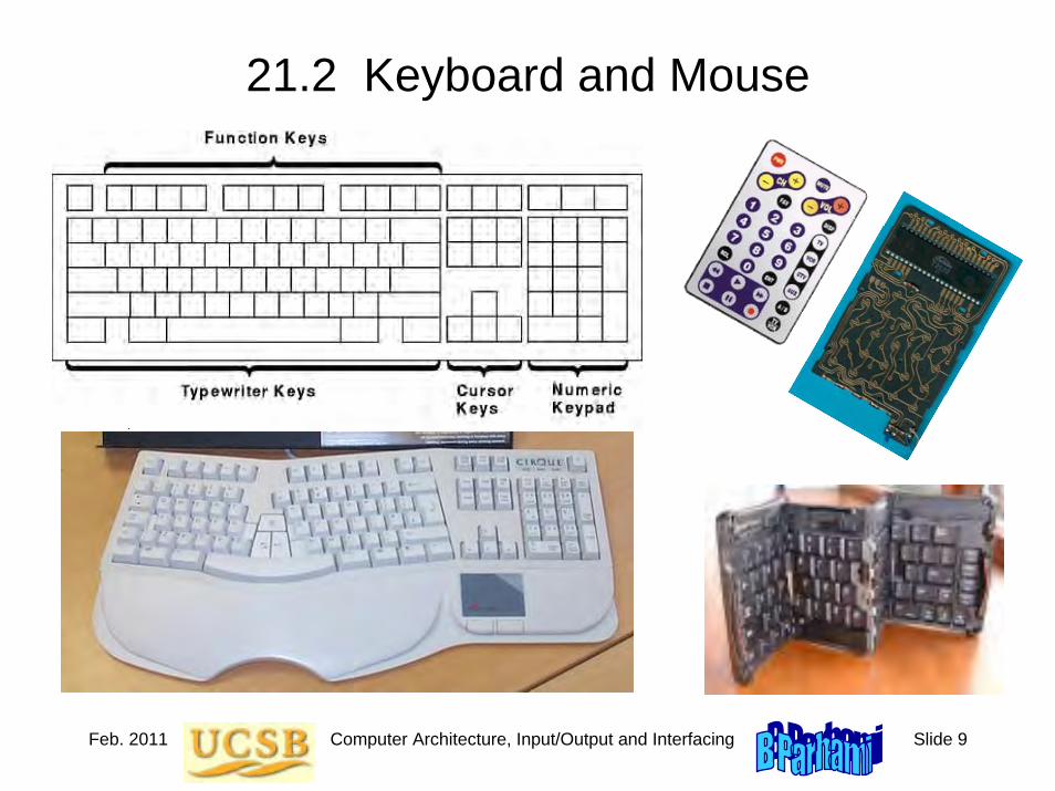
Feb. 2011 Computer Architecture, Input/Output and Interfacing Slide 9
21.2 Keyboard and Mouse

Feb. 2011 Computer Architecture, Input/Output and Interfacing Slide 10
Keyboard Switches and Encoding
Key cap
(a) Mechanical switch with a plunger
Contacts
Spring
(b) Membrane switch
Conductor-coated membrane
(c) Logical arrangement of keys
0 1 2 3
c d e f
8 9 a b
4 5 6 7
Figure 21.3 Two mechanical switch designs and the logical layout of a hex keypad.

Feb. 2011 Computer Architecture, Input/Output and Interfacing Slide 11
Projection Virtual Keyboard
Software:Emulates a real keyboard, even clicking key sounds
Hardware:A tiny laser device projects the image of a full-size keyboard on any surface

Feb. 2011 Computer Architecture, Input/Output and Interfacing Slide 12
Pointing Devices

Feb. 2011 Computer Architecture, Input/Output and Interfacing Slide 13
How a Mouse Works
Figure 21.4 Mechanical and simple optical mice.
x roller
(a) Mechanical mouse (b) Optical mouse
Ball touching the rollers rotates them via friction
y roller
y axis
x axis
Mouse pad
Photosensor detects crossing of grid lines

Feb. 2011 Computer Architecture, Input/Output and Interfacing Slide 14
21.3 Visual Display Units
Figure 21.5 CRT display unit and image storage in frame buffer.
Frame buffer
x
y
Pixel info: brightness, color, etc.
Electron gun
Sensitive screen
Electron beam
≅ 1K lines
≅ 1K pixels per line
(a) Image formation on a CRT (b) Data defining the image
Deflection coils

Feb. 2011 Computer Architecture, Input/Output and Interfacing Slide 15
How Color CRT Displays Work
Figure 21.6 The RGB color scheme of modern CRT displays.
Direction of red beam
(a) The RGB color stripes (b) Use of shadow mask
Direction of green beam
Direction of blue beam
Faceplate
Shadow mask
R G B R G B R G B R G B R G B R G B
R G B
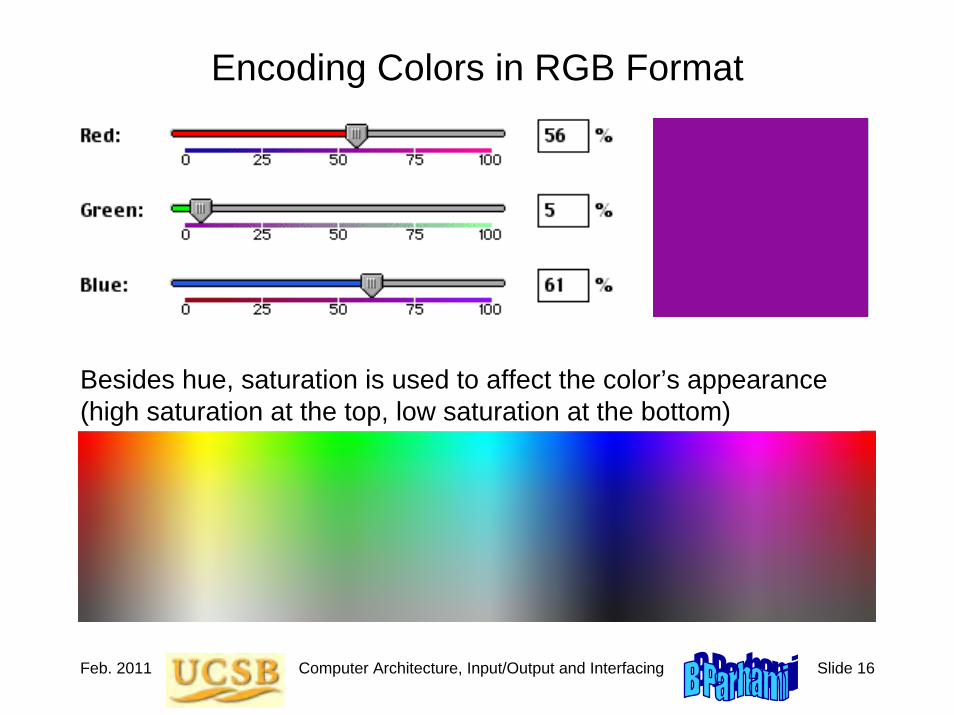
Feb. 2011 Computer Architecture, Input/Output and Interfacing Slide 16
Encoding Colors in RGB Format
Besides hue, saturation is used to affect the color’s appearance(high saturation at the top, low saturation at the bottom)

Feb. 2011 Computer Architecture, Input/Output and Interfacing Slide 17
Flat-Panel Displays
Figure 21.7 Passive and active LCD displays.
(a) Passive display (b) Active display
Column pulses Column pulses
Address pulse
Column (data) lines Column (data) lines
Row lines

Feb. 2011 Computer Architecture, Input/Output and Interfacing Slide 18
Flexible Display DevicesPaper-thin tablet-size display unit by E Ink
Sony organic light-emitting diode (OLED) flexible display

Feb. 2011 Computer Architecture, Input/Output and Interfacing Slide 19
Other Display Technologies
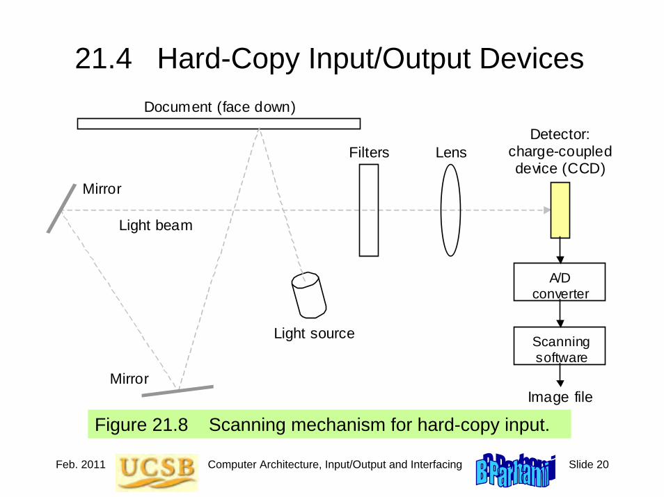
Feb. 2011 Computer Architecture, Input/Output and Interfacing Slide 20
21.4 Hard-Copy Input/Output Devices
Figure 21.8 Scanning mechanism for hard-copy input.
Document (face down)
Mirror
Mirror
Light source
Filters Lens Detector:
charge-coupled device (CCD)
Light beam
A/D converter
Scanning software
Image file

Feb. 2011 Computer Architecture, Input/Output and Interfacing Slide 21
Character Formation by Dot Matrices
Figure 21.9 Forming the letter “D” via dot matrices of varying sizes.
oooooooooooooo ooooooooooooooooo oo oooo oo ooo oo oo oo oo oo oo oo oo oo oo oo o oo oo oo oo oo oo oo oo oo oo oo oo oo oo oo oo oo oo oo oo oo oo oo oo oo oo oo oo oo oo oo oo oo oo oo oo oo oo oo o oo oo oo oo oo oo oo oo oo oo oo ooo oo oooo ooooooooooooooooo oooooooooooooo
ooooo o o o o o o o o o o o o o o ooooo
ooooooooo o oo o oo o o o o o o o o o o o o o o o o o o o o o o o o o o o o o o o oo o oo ooooooooo
oooooooooooooo ooooooooooooooooo oo oooo oo ooo oo oo oo oo oo oo oo oo oo oo oo o oo oo oo oo oo oo oo oo oo oo oo oo oo oo oo oo oo oo oo oo oo oo oo oo oo oo oo oo oo oo oo oo oo oo oo oo oo oo oo o oo oo oo oo oo oo oo oo oo oo oo ooo oo oooo ooooooooooooooooo oooooooooooooo
ooooo oo oo o o o o o o o o o o o o o o o oo oo ooooo
Same dot matrix size,but with greater resolution

Feb. 2011 Computer Architecture, Input/Output and Interfacing Slide 22
Simulating Intensity Levels via Dithering
Forming five gray levels on a device that supports only black and white (e.g., ink-jet or laser printer)
Using the dithering patterns above on each of three colors forms 5 × 5 × 5 = 125 different colors

Feb. 2011 Computer Architecture, Input/Output and Interfacing Slide 23
Simple Dot-Matrix Printer Mechanism

Feb. 2011 Computer Architecture, Input/Output and Interfacing Slide 24
Common Hard-Copy Output Devices
Figure 21.10 Ink-jet and laser printers.
(a) Ink jet printing
Ink supply
Print head
Ink droplet
Print head movement
Paper movement
Sheet of paper
(b) Laser printing
Print head assembly
Rollers
Sheet of paper
Light from optical system
Toner
Rotating drum
Cleaning of excess toner Corona wire
for charging
Heater
Fusing of toner

Feb. 2011 Computer Architecture, Input/Output and Interfacing Slide 25
How Color Printers Work
The RGB scheme of color monitors is additivvarious amounts of the three primary colorsare added to form a desired color
e:
The CMY scheme of color printers is subtractive:various amounts of the three primary colorsare removed from white to form a desired color
To produce a more satisfactory shade of black, the CMYK scheme is often used (K = black)
RedRed GreenGreen
BlueBlue
CyanCyan MagentaMagenta
YellowYellow
Absence of greenAbsence of green

Feb. 2011 Computer Architecture, Input/Output and Interfacing Slide 26
The CMYK Printing Process
Illusion of full colorcreated with CMYK dots

Feb. 2011 Computer Architecture, Input/Output and Interfacing Slide 27
Color Wheels
Artist’s color wheel,used for mixing paint
Subtractive color wheel,used in printing (CMYK)
Additive color wheel,used for projection
Primary colors appear at center and equally spaced around the perimeterSecondary colors are midway between primary colorsTertiary colors are between primary and secondary colors
Source of this and several other slides on color: http://www.devx.com/projectcool/Article/19954/0/(see also color theory tutorial: http://graphics.kodak.com/documents/Introducing%20Color%20Theory.pdf)

Feb. 2011 Computer Architecture, Input/Output and Interfacing Slide 28
21.5 Other Input/Output Devices

Feb. 2011 Computer Architecture, Input/Output and Interfacing Slide 29
Sensors and Actuators
• Light sensors (photocells)• Temperature sensors (contact and noncontact types)• Pressure sensors
Collecting info about the environment and other conditions
S
S
N
N
N
N
N
S
S
S
(a) Initial state
N
N S
S N
N N
S
S
S
(a) After rotation Figure 21.11 Stepper motor principles of operation.

Feb. 2011 Computer Architecture, Input/Output and Interfacing Slide 30
Screw
Converting Circular Motion to Linear Motion
Locomotive
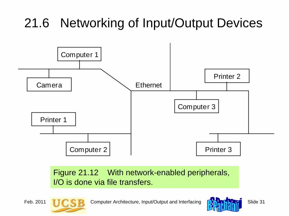
Feb. 2011 Computer Architecture, Input/Output and Interfacing Slide 31
21.6 Networking of Input/Output Devices
Figure 21.12 With network-enabled peripherals, I/O is done via file transfers.
Printer 1
Printer 3
Printer 2
Computer 1
Ethernet
Computer 2
Computer 3
Camera

Feb. 2011 Computer Architecture, Input/Output and Interfacing Slide 32
Input/Output in Control and Embedded Systems
Figure 21.13 The structure of a closed-loop computer-based control system.
Analog signal
conditioning
Digital signal
conditioning
Signal conversion
Signal conversion
Analog sensors: thermocouples, pressure sensors, ...
Digital sensors: detectors, counters, on/off switches, ...
Digital actuators: stepper motors, relays, alarms, ...
Analog actuators: valves, pumps, speed regulators, ...
Digital output
interface
D/A output
interface
Digital input
interface
A/D input interface
CPU and memory
Network interface
Intelligent devices, other computers, archival storage, ...
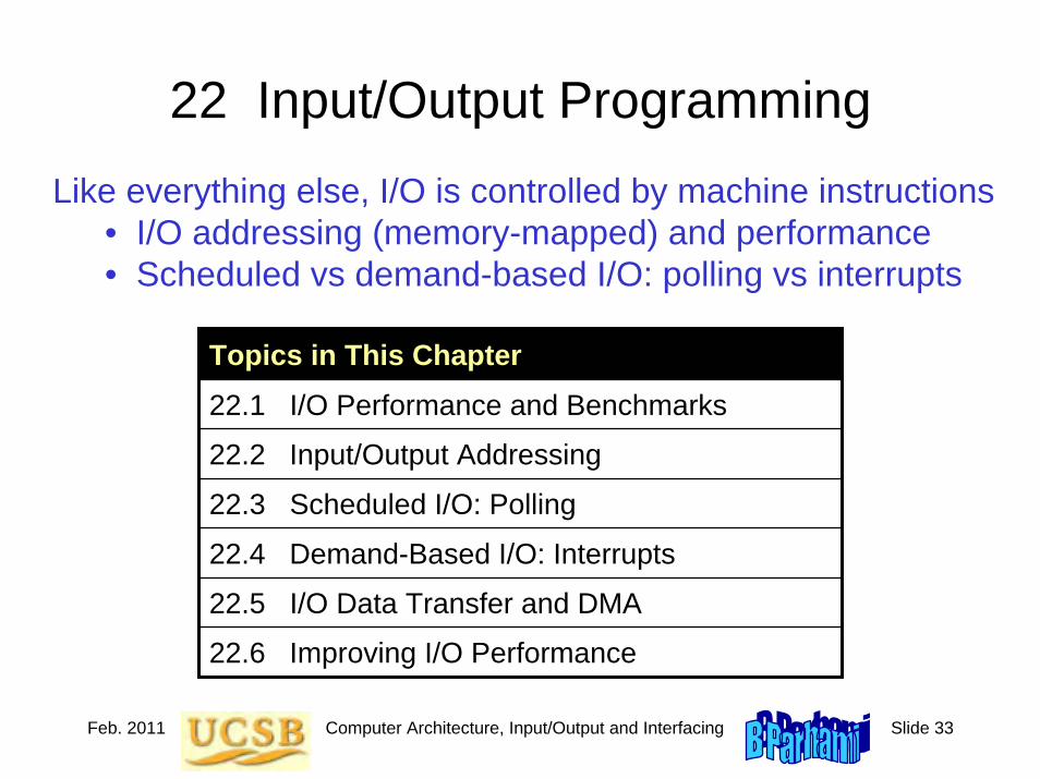
Feb. 2011 Computer Architecture, Input/Output and Interfacing Slide 33
22 Input/Output ProgrammingLike everything else, I/O is controlled by machine instructions
• I/O addressing (memory-mapped) and performance• Scheduled vs demand-based I/O: polling vs interrupts
Topics in This Chapter22.1 I/O Performance and Benchmarks
22.2 Input/Output Addressing
22.3 Scheduled I/O: Polling
22.4 Demand-Based I/O: Interrupts
22.5 I/O Data Transfer and DMA
22.6 Improving I/O Performance

Feb. 2011 Computer Architecture, Input/Output and Interfacing Slide 34
22.1 I/O Performance and Benchmarks Example 22.1: The I/O wall
An industrial control application spent 90% of its time on CPU operations when it was originally developed in the early 1980s. Since then, the CPU component has been upgraded every 5 years, but the I/O components have remained the same. Assuming that CPU performance improved tenfold with each upgrade, derive the fraction of time spent on I/O over the life of the system.
Solution
Apply Amdahl’s law with 90% of the task speeded up by factors of10, 100, 1000, and 10000 over a 20-year period. In the course of these upgrades the running time has been reduced from the original 1 to 0.1 + 0.9/10 = 0.19, 0.109, 0.1009, and 0.10009, making thefraction of time spent on input/output 52.6, 91.7, 99.1, and 99.9%, respectively. The last couple of CPU upgrades did not really help.

Feb. 2011 Computer Architecture, Input/Output and Interfacing Slide 35
Types of Input/Output BenchmarkSupercomputer I/O benchmarks
Reading large volumes of input dataWriting many snapshots for checkpointingSaving a relatively small set of resultsI/O data throughput, in MB/s, is important
Transaction processing I/O benchmarks
Huge database, but each transaction fairly smallA handful (2-10) of disk accesses per transactionI/O rate (disk accesses per second) is important
File system I/O benchmarksFile creation, directory management, indexing, . . .Benchmarks are usually domain-specific

Feb. 2011 Computer Architecture, Input/Output and Interfacing Slide 36
22.2 Input/Output Addressing
Figure 22.1 Control and data registers for keyboard and display unit in MiniMIPS.
Keyboard control 0xffff0000
Memory location (hex address)
0xffff0004 Keyboard data
R I E
Display control 0xffff0008
0xffff000c Display data
R I E
Device ready Interrupt enable
Data byte
Data byte
32-bit device registers
0 1 7 31 2 3 4 5 6
0 1 7 31 2 3 4 5 6

Feb. 2011 Computer Architecture, Input/Output and Interfacing Slide 37
Hardware for I/O Addressing
Figure 22.2 Addressing logic for an I/O device controller.
Control Address
Data
Memory bus
Compare
Device address
Control logic Device
controller
Device status
Device data
=

Feb. 2011 Computer Architecture, Input/Output and Interfacing Slide 38
Keyboard 0xffff0000
Memory location (hex address)
0xffff0004 Keyboard
R I E
Display co0xffff0008
0xffff000c Display da
R I E
Device readInterrupt enable
Data byte
Data byte
32-bit device registers
0 1 7 31 2 3 4 5 6
0 1 7 31 2 3 4 5 6
Data Input from KeyboardExample 22.2
Write a sequence of MiniMIPS assembly language instructions to make the program wait until the keyboard has a symbol to transmit and then read the symbol into register $v0.
Solution
The program must continually examine the keyboard control register, ending its “busy wait” when the R bit has been asserted.
lui $t0,0xffff # put 0xffff0000 in $t0idle: lw $t1,0($t0) # get keyboard’s control word
andi $t1,$t1,0x0001 # isolate the LSB (R bit)beq $t1,$zero,idle # if not ready (R = 0), waitlw $v0,4($t0) # retrieve data from keyboard
This type of input is appropriate only if the computer is waiting for a critical input and cannot continue in the absence of such input.

Feb. 2011 Computer Architecture, Input/Output and Interfacing Slide 39
Keyboa0xffff0000
Memory location (hex address)
0xffff0004 Keyboa
R I E
Display 0xffff0008
0xffff000c Display
R I E
Device reInterrupt enable
Data byte
Data byte
32-bit device registers
0 1 7 31 2 3 4 5 6
0 1 7 31 2 3 4 5 6
Data Output to Display UnitExample 22.3
Write a sequence of MiniMIPS assembly language instructions to make the program wait until the display unit is ready to accept a new symbol and then write the symbol from $a0 to the display unit.
Solution
The program must continually examine the display unit’s control register, ending its “busy wait” when the R bit has been asserted.
lui $t0,0xffff # put 0xffff0000 in $t0idle: lw $t1,8($t0) # get display’s control word
andi $t1,$t1,0x0001 # isolate the LSB (R bit)beq $t1,$zero,idle # if not ready (R = 0), waitsw $a0,12($t0) # supply data to display unit
This type of output is appropriate only if we can afford to have the CPU dedicated to data transmission to the display unit.

Feb. 2011 Computer Architecture, Input/Output and Interfacing Slide 40
22.3 Scheduled I/O: PollingExamples 22.4, 22.5, 22.6
What fraction of a 1 GHz CPU’s time is spent polling the following devices if each polling action takes 800 clock cycles?
Keyboard must be interrogated at least 10 times per secondFloppy sends data 4 bytes at a time at a rate of 50 KB/sHard drive sends data 4 bytes at a time at a rate of 3 MB/s
Solution
For keyboard, divide the number of cycles needed for 10 interrogations by the total number of cycles available in 1 second:
(10 × 800)/109 ≅ 0.001%The floppy disk must be interrogated 50K/4 = 12.5K times per sec
(12.5K × 800)/109 ≅ 1%The hard disk must be interrogated 3M/4 = 750K times per sec
(750K × 800)/109 ≅ 60%
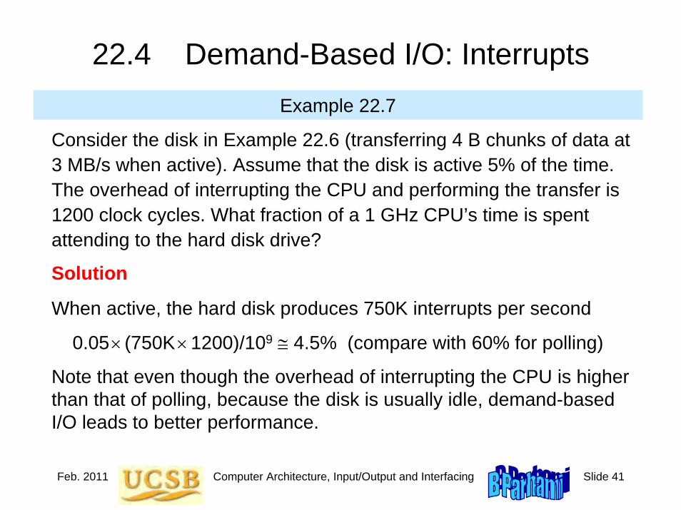
Feb. 2011 Computer Architecture, Input/Output and Interfacing Slide 41
22.4 Demand-Based I/O: InterruptsExample 22.7
Consider the disk in Example 22.6 (transferring 4 B chunks of data at 3 MB/s when active). Assume that the disk is active 5% of the time. The overhead of interrupting the CPU and performing the transfer is 1200 clock cycles. What fraction of a 1 GHz CPU’s time is spent attending to the hard disk drive?
Solution
When active, the hard disk produces 750K interrupts per second
0.05× (750K×1200)/109 ≅ 4.5% (compare with 60% for polling)
Note that even though the overhead of interrupting the CPU is higher than that of polling, because the disk is usually idle, demand-based I/O leads to better performance.

Feb. 2011 Computer Architecture, Input/Output and Interfacing Slide 42
Interrupt HandlingUpon detecting an interrupt signal, provided the particular interrupt or interrupt class is not masked, the CPU acknowledgesthe interrupt (so that the device can deassert its request signal) and begins executing an interrupt service routine.
1. Save the CPU state and call the interrupt service routine. 2. Disable all interrupts.3. Save minimal information about the interrupt on the stack.4. Enable interrupts (or at least higher priority ones).5. Identify cause of interrupt and attend to the underlying request.6. Restore CPU state to what existed before the last interrupt.7. Return from interrupt service routine.
The capability to handle nested interrupts is important in dealing with multiple high-speed I/O devices.

Feb. 2011 Computer Architecture, Input/Output and Interfacing Slide 43
22.5 I/O Data Transfer and DMA
Figure 22.3 DMA controller shares the system or memory bus with the CPU.
Other control
Address Data
System bus
CPU and
cache
Bus request
ReadWrite’ DataReady’
Main memory
Typical I/O
device Bus grant
DMA controller
Length Status
Dest’n Source

Feb. 2011 Computer Architecture, Input/Output and Interfacing Slide 44
DMA Operation
Figure 22.4 DMA operation and the associated transfers of bus control.
CPU
(a) DMA transfer in one continuous burst
BusRequest BusGrant
DMA
CPU
(b) DMA transfer in several shorter bursts
BusRequest BusGrant
DMA

Feb. 2011 Computer Architecture, Input/Output and Interfacing Slide 45
22.6 Improving I/O PerformanceExample 22.9: Effective I/O bandwidth from disk
Consider a hard disk drive with 512 B sectors, average access latency of 10 ms, and peak throughput of 10 MB/s. Plot the variation of the effective I/O bandwidth as the unit of data transfer (block) varies in size from 1 sector (0.5 KB) to 1024 sectors (500 KB).
Solution
400
10
Thro
ughp
ut (M
B /
s)
Block size (KB) 300 200 100 0 500
0
6
4
2
8
Figure 22.50.05 MB/s
5 MB/s

Feb. 2011 Computer Architecture, Input/Output and Interfacing Slide 46
Computing the Effective ThroughputElaboration on Example 22.9: Effective I/O bandwidth from disk
Total access time for x bytes = 10 ms + xfer time = (0.01 + 10–7x) sEffective access time per byte = (0.01 + 10–7x)/x s/BEffective transfer rate = x/(0.01 + 10–7x) B/sFor x = 100 KB: Effective transfer rate = 105/(0.01 + 10–2) = 5×10⁶ B/s
400
10
Thro
ughp
ut (M
B /
s)
Block size (KB) 300 200 100 0 500
0
6
4
2
8
Figure 22.50.05 MB/s
5 MB/s
Averageaccess latency = 10 ms
Peakthroughput = 10 MB/s

Feb. 2011 Computer Architecture, Input/Output and Interfacing Slide 47
Distributed Input/Output
Figure 22.6 Example configuration for the Infiniband distributed I/O.
To other subnets
HCA
CPU
Mem
CPU
HCA
CPU
Mem
CPU
I/O
HCA
I/O
HCA
I/O
HCA
I/O
HCA
I/O
HCA
Router
Switch
Switch Switch
HCA = Host channel adapter
Module with built-in switch

Feb. 2011 Computer Architecture, Input/Output and Interfacing Slide 48
23 Buses, Links, and InterfacingShared links or buses are common in modern computers:
• Fewer wires and pins, greater flexibility & expandability• Require dealing with arbitration and synchronization
Topics in This Chapter
23.1 Intra- and Intersystem Links
23.2 Buses and Their Appeal
23.3 Bus Communication Protocols
23.4 Bus Arbitration and Performance
23.5 Basics of Interfacing
23.6 Interfacing Standards
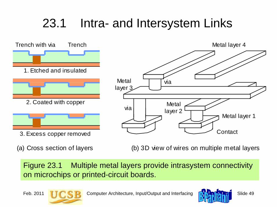
Feb. 2011 Computer Architecture, Input/Output and Interfacing Slide 49
23.1 Intra- and Intersystem Links
Figure 23.1 Multiple metal layers provide intrasystem connectivity on microchips or printed-circuit boards.
Trench
1. Etched and insulated
2. Coated with copper
3. Excess copper removed
Trench with via
(a) Cross section of layers (b) 3D view of wires on multiple metal layers
Contact
Metal layer 1
Metal layer 2
Metal layer 4
via
via
Metal layer 3

Feb. 2011 Computer Architecture, Input/Output and Interfacing Slide 50
Multiple Metal Layers on a Chip or PC Board
Cross section of metal layers
Active elements and their connectors
Modern chips have 8-9 metal layers
Upper layers carry longer wires as well as those that need more power
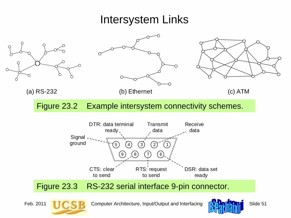
Feb. 2011 Computer Architecture, Input/Output and Interfacing Slide 51
Intersystem Links
Figure 23.2 Example intersystem connectivity schemes.
Computer
(a) RS-232 (b) Ethernet (c) ATM
Figure 23.3 RS-232 serial interface 9-pin connector.
Receive data
Signal ground
DTR: data terminal ready
Transmit data
DSR: data set ready
RTS: request to send
CTS: clear to send
1 2 3 4
6 7 8 9
5

Feb. 2011 Computer Architecture, Input/Output and Interfacing Slide 52
Intersystem Communication Media
Coaxial cable
Outer conductor
Copper core
Insulator
Plastic
Twisted pair
Optical fiber Light
source
Reflection Silica
Figure 23.4 Commonly used communication media for intersystem connections.

Feb. 2011 Computer Architecture, Input/Output and Interfacing Slide 53
Comparing Intersystem Links
Table 23.1 Summary of three interconnection schemes.
Interconnection properties RS-232 Ethernet ATM
Maximum segment length (m) 10s 100s 1000s
Maximum network span (m) 10s 100s Unlimited
Bit rate (Mb/s) Up to 0.02 10/100/1000 155-2500
Unit of transmission (B) 1 100s 53
Typical end-to-end latency (ms) < 1 10s-100s 100s
Typical application domain Input/Output LAN Backbone
Transceiver complexity or cost Low Low High

Feb. 2011 Computer Architecture, Input/Output and Interfacing Slide 54
23.2 Buses and Their Appeal
Point-to-point connections between n units require n(n – 1) channels, or n(n – 1)/2 bidirectional links; that is, O(n2) links
0 2
3n–1
1
n–2
0 2
3n–1
1
n–2
Bus connectivity requires only one input and one output port per unit,or O(n) links in all
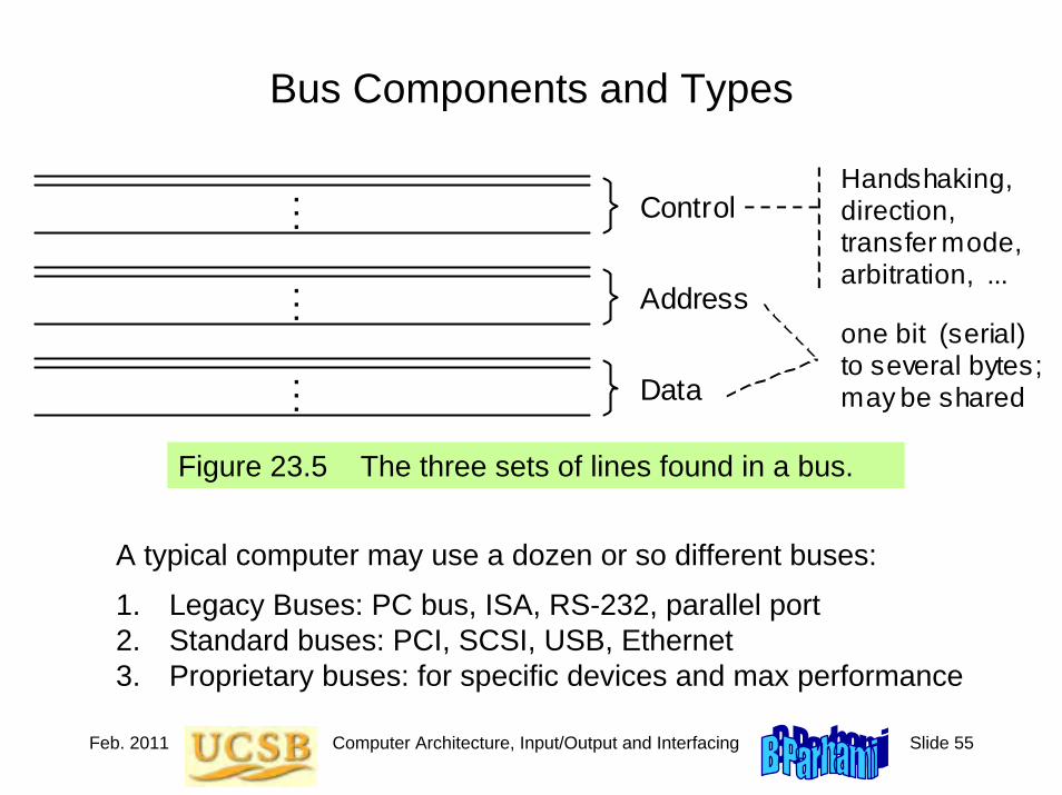
Feb. 2011 Computer Architecture, Input/Output and Interfacing Slide 55
Bus Components and Types
Figure 23.5 The three sets of lines found in a bus.
Control . . .
. . .
. . .
Address
Data
Handshaking, direction, transfer mode, arbitration, ...
one bit (serial) to several bytes; may be shared
A typical computer may use a dozen or so different buses:
1. Legacy Buses: PC bus, ISA, RS-232, parallel port2. Standard buses: PCI, SCSI, USB, Ethernet3. Proprietary buses: for specific devices and max performance

Feb. 2011 Computer Architecture, Input/Output and Interfacing Slide 56
23.3 Bus Communication Protocols
Figure 23.6 Synchronous bus with fixed-latency devices.
Clock
Address placed on the bus
Wait Wait Data availability ensured
Address
Data Wait
Request
Address or data
Ack
Ready
Figure 23.7 Handshaking on an asynchronous bus for an input operation (e.g., reading from memory).
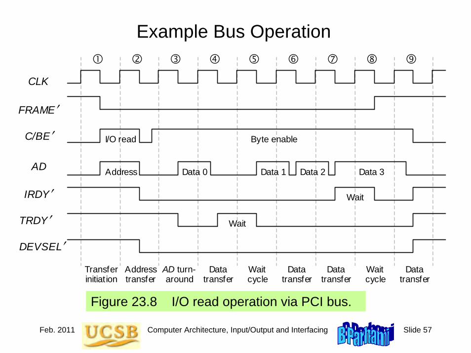
Feb. 2011 Computer Architecture, Input/Output and Interfacing Slide 57
Example Bus Operation
Figure 23.8 I/O read operation via PCI bus.
CLK
FRAME′ C/BE′
AD
DEVSEL′
TRDY′
IRDY′
I/O read Byte enable
Address Data 0 Data 1 Data 2 Data 3
Wait
Wait
AD turn- around
Data transfer
Data transfer
Data transfer
Data transfer
Wait cycle
Wait cycle
Address transfer
Transfer initiat ion

Feb. 2011 Computer Architecture, Input/Output and Interfacing Slide 58
23.4 Bus Arbitration and Performance
Figure 23.9 General structure of a centralized bus arbiter.
Arbiter . . .
. . . . . .
Bus release
R n−1
R 0 R 1 R 2
G n−1
G 0 G 1 G 2
S y n c
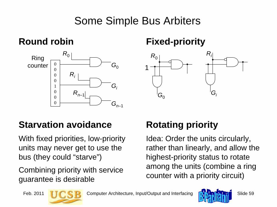
Feb. 2011 Computer Architecture, Input/Output and Interfacing Slide 59
Some Simple Bus Arbiters
Round robin
Rotating priorityIdea: Order the units circularly, rather than linearly, and allow the highest-priority status to rotate among the units (combine a ring counter with a priority circuit)
Starvation avoidanceWith fixed priorities, low-priority units may never get to use the bus (they could “starve”)
Combining priority with service guarantee is desirable
00001000
R0
G0
Ring counter
Ri
GiRn–1
Gn–1
Fixed-priorityRiR0
GiG0
1

Feb. 2011 Computer Architecture, Input/Output and Interfacing Slide 60
Daisy Chaining
Figure 23.9 Daisy chaining allows a small centralized arbiter to service a large number of devices that use a shared resource.
Arbiter . . .
. . . . . .
Bus release
R 0 R 1 R 2
G 0 G 1 G 2
S y n c
Device A
Device B
Device C
Device D
Bus request
Bus grant
Daisy chain of devices
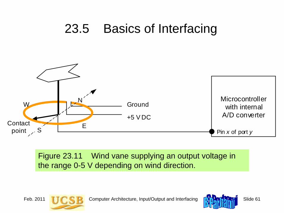
Feb. 2011 Computer Architecture, Input/Output and Interfacing Slide 61
23.5 Basics of Interfacing
Figure 23.11 Wind vane supplying an output voltage in the range 0-5 V depending on wind direction.
Ground
+5 V DC E
W Microcontroller
with internal A/D converter
Pin x of port y Contact
point S
N

Feb. 2011 Computer Architecture, Input/Output and Interfacing Slide 62
23.6 Interfacing StandardsTable 23.2 Summary of four standard interface buses.
Attributes ↓ Name → PCI SCSI FireWire USB
Type of bus Backplane Parallel I/O Serial I/O Serial I/OStandard designation PCI ANSI X3.131 IEEE 1394 USB 2.0
Typical application domain System Fast I/O Fast I/O Low-cost I/OBus width (data bits) 32-64 8-32 2 1
Peak bandwidth (MB/s) 133-512 5-40 12.5-50 0.2-15Maximum number of devices 1024* 7-31# 63 127$
Maximum span (m) < 1 3-25 4.5-72$ 5-30$
Arbitration method Centralized Self-select Distributed Daisy chainTransceiver complexity or cost High Medium Medium Low
Notes: * 32 per bus segment; # One less than bus width; $ With hubs (repeaters)
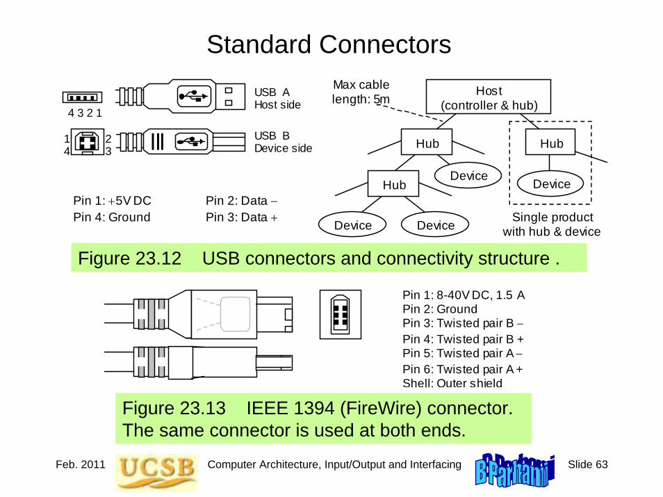
Feb. 2011 Computer Architecture, Input/Output and Interfacing Slide 63
Standard Connectors
Figure 23.12 USB connectors and connectivity structure .
Figure 23.13 IEEE 1394 (FireWire) connector. The same connector is used at both ends.
Pin 1: +5V DC Pin 4: Ground
4 3 2 1
USB A Host side USB B Device side
Pin 2: Data − Pin 3: Data +
Host (controller & hub)
Hub Hub
Hub Device
Device Device
Device
Single product with hub & device
Max cable length: 5m
1 4
2 3
Pin 1: 8-40V DC, 1.5 A Pin 2: Ground Pin 3: Twisted pair B − Pin 4: Twisted pair B + Pin 5: Twisted pair A − Pin 6: Twisted pair A + Shell: Outer shield
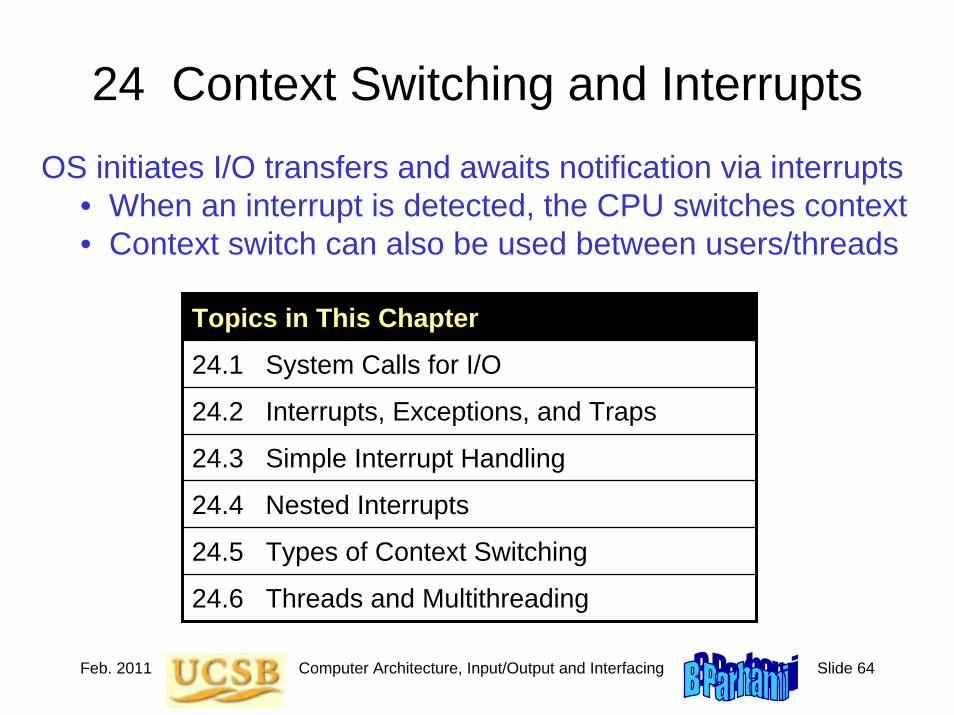
Feb. 2011 Computer Architecture, Input/Output and Interfacing Slide 64
24 Context Switching and InterruptsOS initiates I/O transfers and awaits notification via interrupts
• When an interrupt is detected, the CPU switches context• Context switch can also be used between users/threads
Topics in This Chapter
24.1 System Calls for I/O
24.2 Interrupts, Exceptions, and Traps
24.3 Simple Interrupt Handling
24.4 Nested Interrupts
24.5 Types of Context Switching
24.6 Threads and Multithreading

Feb. 2011 Computer Architecture, Input/Output and Interfacing Slide 65
24.1 System Calls for I/OWhy the user must be isolated from details of I/O operations
Protection: User must be barred from accessing some disk areas
Convenience: No need to learn details of each device’s operation
Efficiency: Most users incapable of finding the best I/O scheme
I/O abstraction: grouping of I/O devices into a small number ofgeneric types so as to make the I/O device-independent
Character stream I/O: get(●), put(●) – e.g., keyboard, printer
Block I/O: seek(●), read(●), write(●) – e.g., disk
Network Sockets: create socket, connect, send/receive packet
Clocks or timers: set up timer (get notified via an interrupt)

Feb. 2011 Computer Architecture, Input/Output and Interfacing Slide 66
24.2 Interrupts, Exceptions, and Traps
Figure 24.1 The notions of interrupts and nested interrupts.
Studying Parhami’s book for test
6:55
Stomach sends interrupt signal
E-mail arrives
7:40
Eating dinner
Reading/sending e-mail
Talk ing on the phone
8:42 9:46
8:53 9:20
8:01
Tele- marketer
calls Best friend
calls
Interrupt Both general term for any diversion and the I/O typeException Caused by an illegal operation (often unpredictable)Trap AKA “software interrupt” (preplanned and not rare)

Feb. 2011 Computer Architecture, Input/Output and Interfacing Slide 67
24.3 Simple Interrupt Handling
Figure 24.2 Simple interrupt logic for the single-cycle MicroMIPS.
Acknowledge the interrupt by asserting the IntAck signalNotify the CPU’s next-address logic that an interrupt is pendingSet the interrupt mask so that no new interrupt is accepted
Interrupt acknowledge
Q R
Q
S
FF
Q R
Q
S
FF
Interrupt mask
IntReq
IntAck
Signals from/to devices
IntEnable
IntDisable
IntAlert
Signals from/to CPU
S y n c

Feb. 2011 Computer Architecture, Input/Output and Interfacing Slide 68
Interrupt Timing
Figure 24.3 Timing of interrupt request and acknowledge signals.
Clock
Synchronized version IntReq
IntAck
IntMask
IntAlert

Feb. 2011 Computer Architecture, Input/Output and Interfacing Slide 69
Next-Address Logic with Interrupts Added
Figure 24.4 Part of the next-address logic for single-cycle MicroMIPS, with an interrupt capability added (compare with the lower left part of Figure 13.4).
SysCallAddr
PCSrc
0 1 2 3
/ 30 / 30 / 30
/ 30
/ 30
IntAlert
IncrPC
NextPC / 30
| jta (PC) 31:28
IntHandlerAddr
0 1
(rs) 31:2
/ 30
Old PC
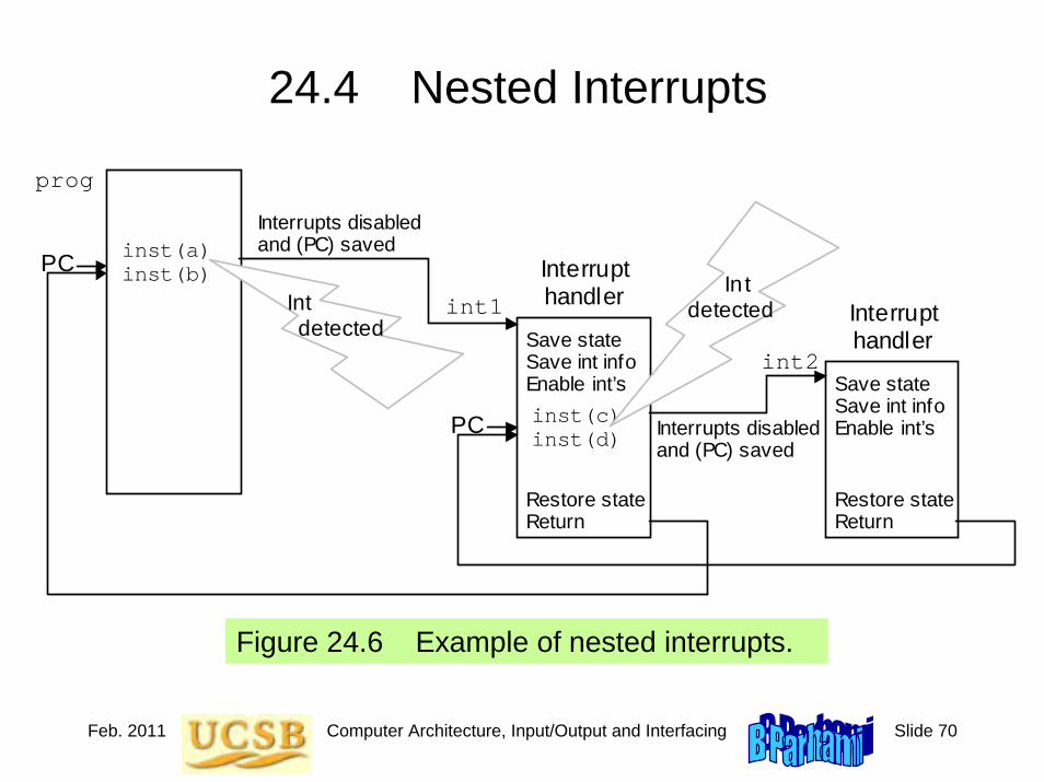
Feb. 2011 Computer Architecture, Input/Output and Interfacing Slide 70
24.4 Nested Interrupts
Figure 24.6 Example of nested interrupts.
inst(a) inst(b)
int1
PC
prog
int2
Interrupt handler
Interrupt handler
Interrupts disabled and (PC) saved
Int detected
Save state Save int info Enable int’s inst(c) inst(d)
Restore state Return
In t detected
Save state Save int info Enable int’s
Restore state Return
Interrupts disabled and (PC) saved
PC

Feb. 2011 Computer Architecture, Input/Output and Interfacing Slide 71
24.5 Types of Context Switching
Figure 24.7 Multitasking in humans and computers.
Taking notes
Talking on telephone
Scanning e-mail messages
(a) Human multitasking (b) Computer multitasking
Task 1 Task 2 Task 3
Context switch
Time slice

Feb. 2011 Computer Architecture, Input/Output and Interfacing Slide 72
24.6 Threads and Multithreading
Figure 24.8 A program divided into tasks (subcomputations) or threads.
(a) Task graph of a program (b) Thread structure of a task
Thread 1 Thread 2 Thread 3
Sync
Sync
Spawn additional threads

Feb. 2011 Computer Architecture, Input/Output and Interfacing Slide 73
Multithreaded Processors
Figure 24.9 Instructions from multiple threads as they make their way through a processor’s execution pipeline.
Threads in memory Issue pipelines Retirement and commit pipeline
Function units Bubble
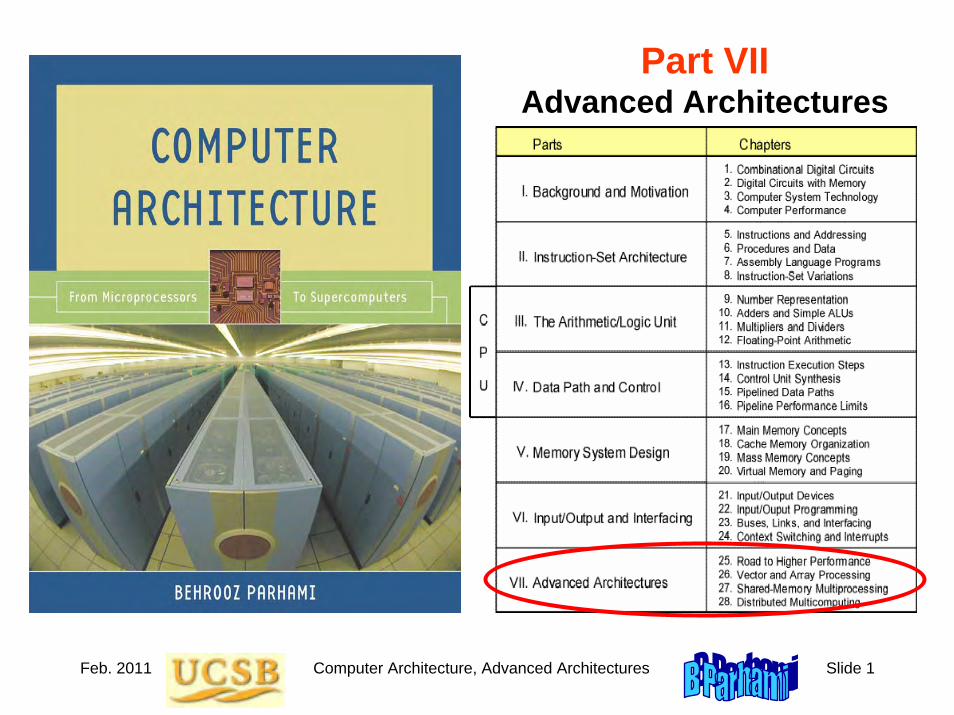
Feb. 2011 Computer Architecture, Advanced Architectures Slide 1
Part VIIAdvanced Architectures

Feb. 2011 Computer Architecture, Advanced Architectures Slide 2
About This PresentationThis presentation is intended to support the use of the textbookComputer Architecture: From Microprocessors to Supercomputers, Oxford University Press, 2005, ISBN 0-19-515455-X. It is updated regularly by the author as part of his teaching of the upper-division course ECE 154, Introduction to Computer Architecture, at the University of California, Santa Barbara. Instructors can use these slides freely in classroom teaching and for other educational purposes. Any other use is strictly prohibited. © Behrooz Parhami
Edition Released Revised Revised Revised RevisedFirst July 2003 July 2004 July 2005 Mar. 2007 Feb. 2011*
* Minimal update, due to this part not being used for lectures in ECE 154 at UCSB

Feb. 2011 Computer Architecture, Advanced Architectures Slide 3
VII Advanced Architectures
Topics in This PartChapter 25 Road to Higher PerformanceChapter 26 Vector and Array ProcessingChapter 27 Shared-Memory MultiprocessingChapter 28 Distributed Multicomputing
Performance enhancement beyond what we have seen:• What else can we do at the instruction execution level?• Data parallelism: vector and array processing• Control parallelism: parallel and distributed processing

Feb. 2011 Computer Architecture, Advanced Architectures Slide 4
25 Road to Higher PerformanceReview past, current, and future architectural trends:
• General-purpose and special-purpose acceleration• Introduction to data and control parallelism
Topics in This Chapter25.1 Past and Current Performance Trends
25.2 Performance-Driven ISA Extensions
25.3 Instruction-Level Parallelism
25.4 Speculation and Value Prediction
25.5 Special-Purpose Hardware Accelerators
25.6 Vector, Array, and Parallel Processing

Feb. 2011 Computer Architecture, Advanced Architectures Slide 5
25.1 Past and Current Performance Trends
0.06 MIPS (4-bit processor)
Intel 4004: The first μp (1971) Intel Pentium 4, circa 2005
10,000 MIPS (32-bit processor)
8008
8080
80848-bit
8086
80186
8028616-bit
8088
80188
80386
Pentium, MMX
Pentium Pro, II32-bit
80486
Pentium III, M
Celeron
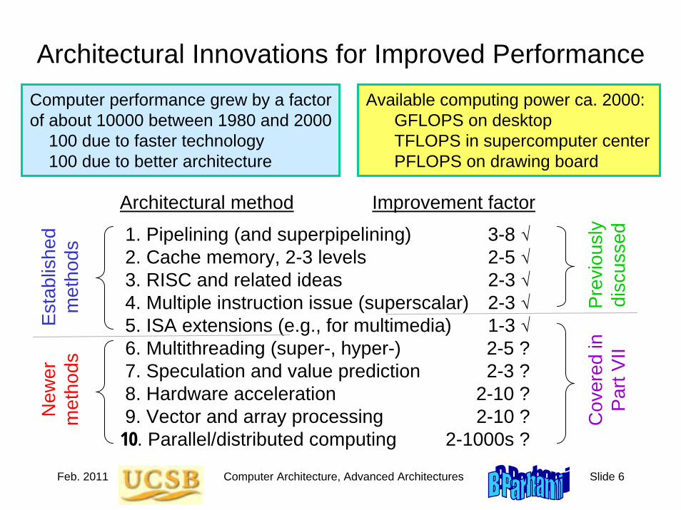
Feb. 2011 Computer Architecture, Advanced Architectures Slide 6
Architectural Innovations for Improved Performance
Architectural method Improvement factor
1. Pipelining (and superpipelining) 3-8 √2. Cache memory, 2-3 levels 2-5 √3. RISC and related ideas 2-3 √4. Multiple instruction issue (superscalar) 2-3 √5. ISA extensions (e.g., for multimedia) 1-3 √6. Multithreading (super-, hyper-) 2-5 ?7. Speculation and value prediction 2-3 ?8. Hardware acceleration 2-10 ?9. Vector and array processing 2-10 ?
10. Parallel/distributed computing 2-1000s ?
Est
ablis
hed
met
hods
New
erm
etho
ds
Pre
viou
sly
disc
usse
dC
over
ed in
Par
t VII
Available computing power ca. 2000:GFLOPS on desktop TFLOPS in supercomputer centerPFLOPS on drawing board
Computer performance grew by a factorof about 10000 between 1980 and 2000
100 due to faster technology 100 due to better architecture

Feb. 2011 Computer Architecture, Advanced Architectures Slide 7
Peak Performance of SupercomputersPFLOPS
TFLOPS
GFLOPS1980 20001990 2010
Earth Simulator
ASCI White Pacific
ASCI Red
Cray T3DTMC CM-5
TMC CM-2Cray X-MP
Cray 2
× 10 / 5 years
Dongarra, J., “Trends in High Performance Computing,”Computer J., Vol. 47, No. 4, pp. 399-403, 2004. [Dong04]
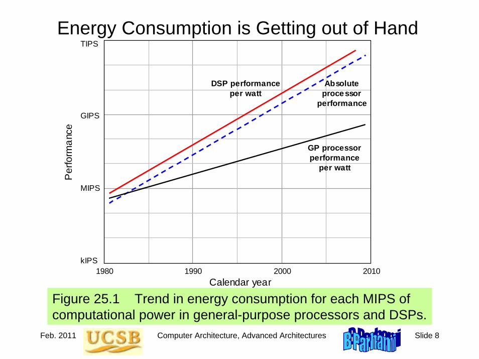
Feb. 2011 Computer Architecture, Advanced Architectures Slide 8
Energy Consumption is Getting out of Hand
Figure 25.1 Trend in energy consumption for each MIPS of computational power in general-purpose processors and DSPs.
1990 1980 2000 2010kIPS
MIPS
GIPS
TIPS
Per
form
ance
Calendar year
Absolute processor
performance
GP processor performance
per watt
DSP performance per watt

Feb. 2011 Computer Architecture, Advanced Architectures Slide 9
25.2 Performance-Driven ISA Extensions
Adding instructions that do more work per cycleShift-add: replace two instructions with one (e.g., multiply by 5)Multiply-add: replace two instructions with one (x := c + a × b)Multiply-accumulate: reduce round-off error (s := s + a × b)Conditional copy: to avoid some branches (e.g., in if-then-else)
Subword parallelism (for multimedia applications)Intel MMX: multimedia extension
64-bit registers can hold multiple integer operands
Intel SSE: Streaming SIMD extension128-bit registers can hold several floating-point operands

Feb. 2011 Computer Architecture, Advanced Architectures Slide 10
Intel MMXISA
Exten-sion
Table25.1
Class Instruction Vector Op type Function or resultsRegister copy 32 bits Integer register ↔ MMX registerParallel pack 4, 2 Saturate Convert to narrower elementsParallel unpack low 8, 4, 2 Merge lower halves of 2 vectorsParallel unpack high 8, 4, 2 Merge upper halves of 2 vectorsParallel add 8, 4, 2 Wrap/Saturate# Add; inhibit carry at boundariesParallel subtract 8, 4, 2 Wrap/Saturate# Subtract with carry inhibitionParallel multiply low 4 Multiply, keep the 4 low halvesParallel multiply high 4 Multiply, keep the 4 high halvesParallel multiply-add 4 Multiply, add adjacent products*Parallel compare equal 8, 4, 2 All 1s where equal, else all 0sParallel compare greater 8, 4, 2 All 1s where greater, else all 0sParallel left shift logical 4, 2, 1 Shift left, respect boundariesParallel right shift logical 4, 2, 1 Shift right, respect boundariesParallel right shift arith 4, 2 Arith shift within each (half)wordParallel AND 1 Bitwise dest ← (src1) ∧ (src2)Parallel ANDNOT 1 Bitwise dest ← (src1) ∧ (src2)′Parallel OR 1 Bitwise dest ← (src1) ∨ (src2)Parallel XOR 1 Bitwise dest ← (src1) ⊕ (src2)Parallel load MMX reg 32 or 64 bits Address given in integer registerParallel store MMX reg 32 or 64 bit Address given in integer register
Control Empty FP tag bits Required for compatibility$
Memoryaccess
Logic
Shift
Arith-metic
Copy

Feb. 2011 Computer Architecture, Advanced Architectures Slide 11
MMX Multiplication and Multiply-Add
Figure 25.2 Parallel multiplication and multiply-add in MMX.
a
(a) Parallel multiply low (b) Parallel multiply-add
b d e
e f g h
s t u v
e × h d × g
b × f a × e
z v
y u
x t
w s
a b d e
e f g h
s + t u + v
e × h d × g
b × f a × e
v
u
t
s
add add

Feb. 2011 Computer Architecture, Advanced Architectures Slide 12
MMX Parallel Comparisons
Figure 25.3 Parallel comparisons in MMX.
14
(a) Parallel compare equal (b) Parallel compare greater
3 58 66
79 1 58 65
0 0 0
5 12 3 32
12 3 22
5 12 6 9
12 5 90 17 8 65 535 (all 1s)
0 0 0 0 0
255 (all 1s)

Feb. 2011 Computer Architecture, Advanced Architectures Slide 13
25.3 Instruction-Level Parallelism
Figure 25.4 Available instruction-level parallelism and the speedup due to multiple instruction issue in superscalar processors [John91].
1
Frac
tion
of c
ycle
s
Issuable instructions per cycle
20%
30%
10%
0% 2 3 4 5 6 7 8 0
Spee
dup
atta
ined
Instruction issue width
3
2
1 2 4 6 8 0
(a) (b)

Feb. 2011 Computer Architecture, Advanced Architectures Slide 14
Instruction-Level Parallelism
Figure 25.5 A computation with inherent instruction-level parallelism.

Feb. 2011 Computer Architecture, Advanced Architectures Slide 15
VLIW and EPIC Architectures
Figure 25.6 Hardware organization for IA-64. General and floating-point registers are 64-bit wide. Predicates are single-bit registers.
VLIW Very long instruction word architectureEPIC Explicitly parallel instruction computing
Memory
General registers (128)
Floating-point registers (128)
Predi- cates (64)
Execution unit
Execution unit
Execution unit
Execution unit
Execution unit
Execution unit . . .
. . .
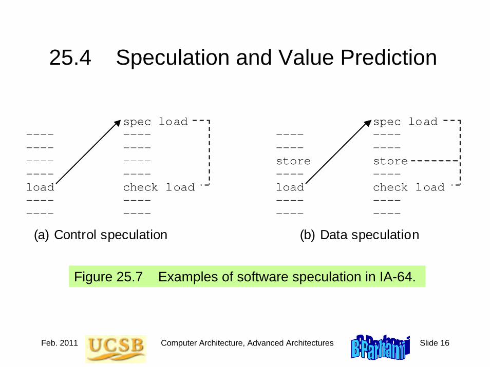
Feb. 2011 Computer Architecture, Advanced Architectures Slide 16
25.4 Speculation and Value Prediction
Figure 25.7 Examples of software speculation in IA-64.
---- ---- ---- ---- load ---- ----
spec load ---- ---- ---- ---- check load ---- ----
(a) Control speculation
---- ---- store ---- load ---- ----
spec load ---- ---- store ---- check load ---- ----
(b) Data speculation

Feb. 2011 Computer Architecture, Advanced Architectures Slide 17
Value Prediction
Figure 25.8 Value prediction for multiplication or division via a memo table.
Mult/ Div
Memo table
Control
Mux
Inputs
Inputs ready
Output
Output ready
0
1
Miss
Done

Feb. 2011 Computer Architecture, Advanced Architectures Slide 18
25.5 Special-Purpose Hardware Accelerators
Figure 25.9 General structure of a processor with configurable hardware accelerators.
CPU Configuration memory
Accel. 1
Accel. 2
Accel. 3
Data and program memory
FPGA-like unit on which accelerators can be formed via loading of configuration registers
Unused resources

Feb. 2011 Computer Architecture, Advanced Architectures Slide 19
Graphic Processors, Network Processors, etc.
Figure 25.10 Simplified block diagram of Toaster2, Cisco Systems’ network processor.
Input buffer
PE 0
PE 1
PE 2
PE 3
PE 4
PE 5 PE
6 PE 7
PE 8
PE 9
PE 10
PE 11
PE 12
PE 13
PE 14
PE 15
Output buffer
Column memory Column
memory Column memory Column
memory
Feedback path
PE5

Feb. 2011 Computer Architecture, Advanced Architectures Slide 20
25.6 Vector, Array, and Parallel Processing
Figure 25.11 The Flynn-Johnson classification of computer systems.
SISD
SIMD
MISD
MIMD
GMSV
GMMP
DMSV
DMMP
Single data stream
Multiple data streams
Sing
le in
str
stre
am
Mul
tiple
inst
r st
ream
s
Flynn’s categories
John
son’
s ex
pans
ion
Shared variables
Message passing
Glo
bal
mem
ory
Dist
ribut
ed
mem
ory
Uniprocessors
Rarely used
Array or vector processors
Mult iproc’s or mult icomputers
Shared-memory mult iprocessors
Rarely used
Distributed shared memory
Distrib-memory mult icomputers

Feb. 2011 Computer Architecture, Advanced Architectures Slide 21
SIMD Architectures
Data parallelism: executing one operation on multiple data streams
Concurrency in time – vector processingConcurrency in space – array processing
Example to provide context
Multiplying a coefficient vector by a data vector (e.g., in filtering)y[i] := c[i] × x[i], 0 ≤ i < n
Sources of performance improvement in vector processing (details in the first half of Chapter 26)
One instruction is fetched and decoded for the entire operationThe multiplications are known to be independent (no checking)Pipelining/concurrency in memory access as well as in arithmetic
Array processing is similar (details in the second half of Chapter 26)

Feb. 2011 Computer Architecture, Advanced Architectures Slide 22
MISD Architecture Example
Figure 25.12 Multiple instruction streams operating on a single data stream (MISD).
I n s t r u c t i o n s t r e a m s 1-5
Data in
Data out

Feb. 2011 Computer Architecture, Advanced Architectures Slide 23
MIMD ArchitecturesControl parallelism: executing several instruction streams in parallel
GMSV: Shared global memory – symmetric multiprocessorsDMSV: Shared distributed memory – asymmetric multiprocessorsDMMP: Message passing – multicomputers
Figure 27.1 Centralized shared memory. Figure 28.1 Distributed memory.
0 0
1 1
m−1
Processor-to-
memory network
Processor-to-
processor network
Processors Memory modules
Parallel I/O
. . .
.
.
.
.
.
.
p−1
0
1
Inter- connection
network
Memories and processors
Par
alle
l inp
ut/o
utpu
t p−1
. . .
Routers
A computing node
. . .

Feb. 2011 Computer Architecture, Advanced Architectures Slide 24
Amdahl’s Law Revisited
0
10
20
40
50
0 10 20 30 40 50Enhancement factor (p )
Spe
edup
(s)
f = 0
f = 0.1
f = 0.05
f = 0.0230
f = 0.01
Figure 4.4 Amdahl’s law: speedup achieved if a fraction f of a task is unaffected and the remaining 1 – f part runs p times as fast.
s =
≤ min(p, 1/f)
1f+ (1 – f)/p
f = sequential fraction
with pprocessors
p = speedup of the rest

Feb. 2011 Computer Architecture, Advanced Architectures Slide 25
26 Vector and Array ProcessingSingle instruction stream operating on multiple data streams
• Data parallelism in time = vector processing• Data parallelism in space = array processing
Topics in This Chapter26.1 Operations on Vectors
26.2 Vector Processor Implementation
26.3 Vector Processor Performance
26.4 Shared-Control Systems
26.5 Array Processor Implementation
26.6 Array Processor Performance

Feb. 2011 Computer Architecture, Advanced Architectures Slide 26
26.1 Operations on Vectors
Sequential processor:
for i = 0 to 63 do P[i] := W[i] × D[i]
endfor
Vector processor:
load Wload DP := W × Dstore P
for i = 0 to 63 do X[i+1] := X[i] + Z[i] Y[i+1] := X[i+1]+Y[i]
endfor
Unparallelizable
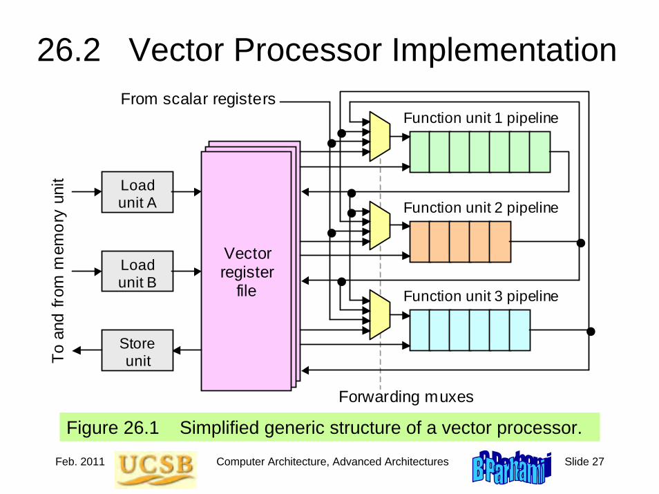
Feb. 2011 Computer Architecture, Advanced Architectures Slide 27
26.2 Vector Processor Implementation
Figure 26.1 Simplified generic structure of a vector processor.
Function unit 1 pipeline
To a
nd fr
om m
emor
y un
it
From scalar registers
Vector register
file
Function unit 2 pipeline
Function unit 3 pipeline
Forwarding muxes
Load unit A
Load unit B
Store unit

Feb. 2011 Computer Architecture, Advanced Architectures Slide 28
Conflict-Free Memory Access
Figure 26.2 Skewed storage of the elements of a 64 × 64 matrix for conflict-free memory access in a 64-way interleaved memory. Elements of column 0 are highlighted in both diagrams .
0,0
2,0 . . .
62,0
63,0
0,1
2,1 . . .
62,1
63,1
0,2
2,2 . . .
62,2
63,2
0,62
2,62 . . .
62,62
63,62
0,63
2,63 . . .
62,63
63,63
...
... . . . ...
...
0,0
2,62 . . .
62,2
63,1
0,1
2,63 . . .
62,3
63,2
0,2
2,0 . . .
62,4
63,3
0,62
2,60 . . .
62,0
63,63
0,63
2,61 . . .
62,1
63,0
...
... . . . ... ...
(a) Conventional row-major order (b) Skewed row-major order
Bank number 0 1 62 63 2 . . . 0 1 62 63 2 . . .
1,0 1,1 1,2 1,62 1,63 ... 1,63 1,0 1,0 1,61 1,62 ...

Feb. 2011 Computer Architecture, Advanced Architectures Slide 29
Overlapped Memory Access and Computation
Figure 26.3 Vector processing via segmented load/store of vectors in registers in a double-buffering scheme. Solid (dashed) lines show data flow in the current (next) segment.
Vector reg 0
Vector reg 1
Vector reg 5
Vector reg 2
Vector reg 3
Vector reg 4
Load X
Load Y
Store Z
To a
nd fr
om m
emor
y un
it
Pipelined adder

Feb. 2011 Computer Architecture, Advanced Architectures Slide 30
26.3 Vector Processor Performance
Figure 26.4 Total latency of the vector computation S := X × Y + Z, without and with pipeline chaining.
Multiplication start-up
Addition start-up
+ ×
+
×
Without chaining
With pipeline chaining
Time
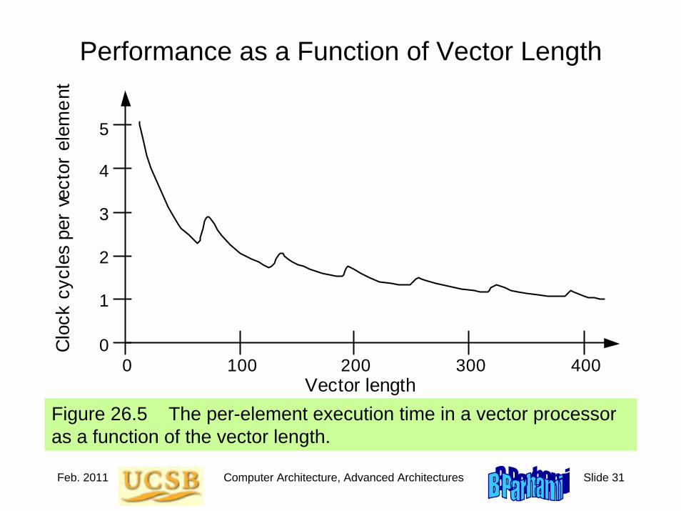
Feb. 2011 Computer Architecture, Advanced Architectures Slide 31
Performance as a Function of Vector Length
Figure 26.5 The per-element execution time in a vector processor as a function of the vector length.
Vector length 100 200 300 400 0
Clo
ck c
ycle
s pe
r ve
ctor
ele
men
t
5
4
3
2
1
0

Feb. 2011 Computer Architecture, Advanced Architectures Slide 32
26.4 Shared-Control Systems
Figure 26.6 From completely shared control to totally separate controls.
(a) Shared-control array processor, SIMD
(b) Multiple shared controls, MSIMD
(c) Separate controls, MIMD
Processing Control
. . .
Processing Control
. . .
Processing Control
. . .
. . .
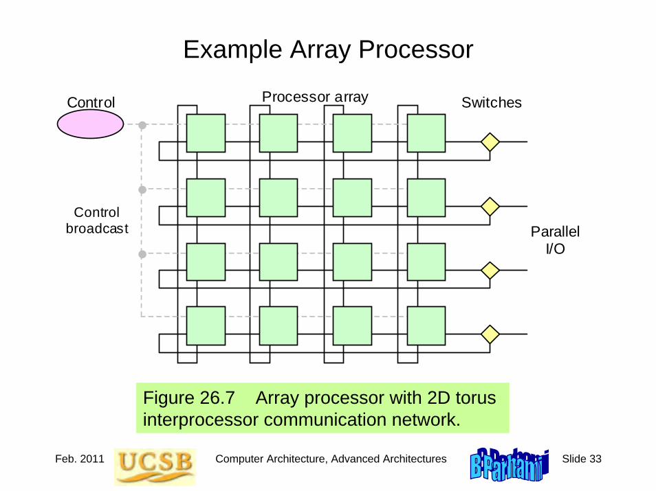
Feb. 2011 Computer Architecture, Advanced Architectures Slide 33
Example Array Processor
Figure 26.7 Array processor with 2D torus interprocessor communication network.
Control broadcast Parallel
I/O
Processor array Control
Switches
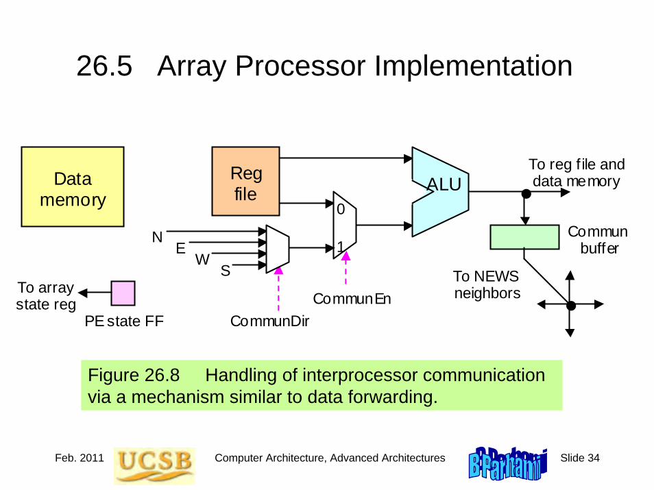
Feb. 2011 Computer Architecture, Advanced Architectures Slide 34
26.5 Array Processor Implementation
Figure 26.8 Handling of interprocessor communication via a mechanism similar to data forwarding.
ALU Reg file
CommunDir CommunEn
PE state FF
Data memory
To array state reg
To reg f ile and data memory
Commun buffer
N E
W S To NEWS
neighbors
0
1
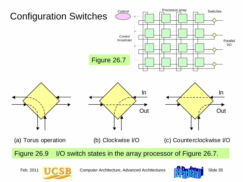
Feb. 2011 Computer Architecture, Advanced Architectures Slide 35
Configuration Switches
Figure 26.9 I/O switch states in the array processor of Figure 26.7.
Control broadcast Parallel
I/O
Processor array Control
Switches
Figure 26.7
(a) Torus operation
In
(b) Clockwise I/O (c) Counterclockwise I/O
Out
In
Out
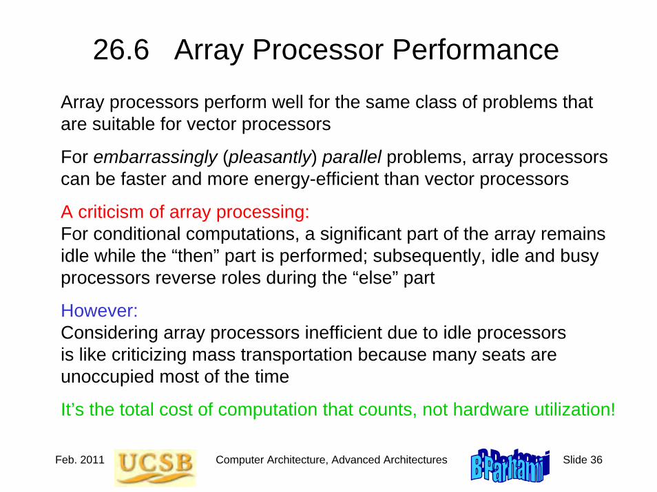
Feb. 2011 Computer Architecture, Advanced Architectures Slide 36
26.6 Array Processor Performance
Array processors perform well for the same class of problems thatare suitable for vector processors
For embarrassingly (pleasantly) parallel problems, array processors
A criticism of array processing:For conditional computations, a significant part of the array remainsidle while the “then” part is performed; subsequently, idle and busyprocessors reverse roles during the “else” part
However:Considering array processors inefficient due to idle processorsis like criticizing mass transportation because many seats are unoccupied most of the time
It’s the total cost of computation that counts, not hardware utilization!
can be faster and more energy-efficient than vector processors

Feb. 2011 Computer Architecture, Advanced Architectures Slide 37
27 Shared-Memory MultiprocessingMultiple processors sharing a memory unit seems naïve
• Didn’t we conclude that memory is the bottleneck?• How then does it make sense to share the memory?
Topics in This Chapter27.1 Centralized Shared Memory
27.2 Multiple Caches and Cache Coherence
27.3 Implementing Symmetric Multiprocessors
27.4 Distributed Shared Memory
27.5 Directories to Guide Data Access
27.6 Implementing Asymmetric Multiprocessors

Feb. 2011 Computer Architecture, Advanced Architectures Slide 38
Parallel Processing as a Topic of Study
Graduate course ECE 254B:Adv. Computer Architecture –Parallel Processing
An important area of studythat allows us to overcomefundamental speed limits
Our treatment of the topic isquite brief (Chapters 26-27)
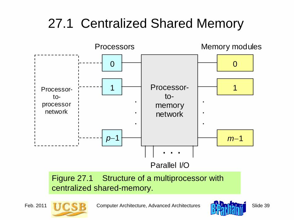
Feb. 2011 Computer Architecture, Advanced Architectures Slide 39
27.1 Centralized Shared Memory
Figure 27.1 Structure of a multiprocessor with centralized shared-memory.
0 0
1 1
m−1
Processor-to-
memory network
Processor-to-
processor network
Processors Memory modules
Parallel I/O
. . .
.
.
.
.
.
.
p−1
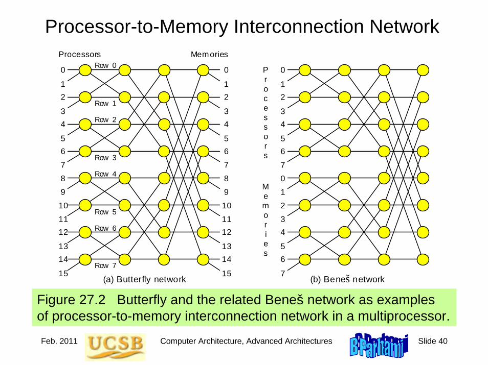
Feb. 2011 Computer Architecture, Advanced Architectures Slide 40
Processor-to-Memory Interconnection Network
Figure 27.2 Butterfly and the related Beneš network as examples of processor-to-memory interconnection network in a multiprocessor.
(a) Butterfly network (b) Beneš network
0
2
4
6
8
10
12
14
Processors Memories
P r o c e s s o r s
M e m o r i e s
1
3
5
7
9
11
13
15
0
2
4
6
8
10
12
14
1
3
5
7
9
11
13
15
0
2
4
6
0
2
4
6
1
3
5
7
1
3
5
7
Row 0
Row 1
Row 2
Row 3
Row 4
Row 5
Row 6
Row 7
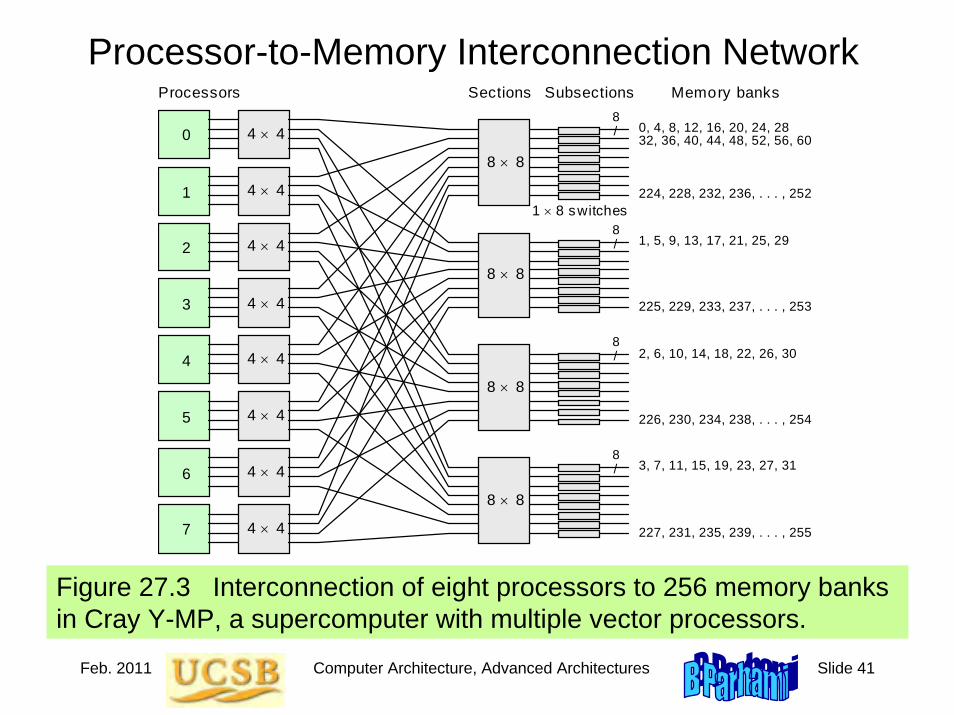
Feb. 2011 Computer Architecture, Advanced Architectures Slide 41
Processor-to-Memory Interconnection Network
Figure 27.3 Interconnection of eight processors to 256 memory banks in Cray Y-MP, a supercomputer with multiple vector processors.
0
1
2
3
4
5
6
7
8 × 8
8 × 8
8 × 8
8 × 8
4 × 4
4 × 4
4 × 4
4 × 4
4 × 4
4 × 4
4 × 4
4 × 4
Sections Subsections Memory banks
0, 4, 8, 12, 16, 20, 24, 28 32, 36, 40, 44, 48, 52, 56, 60
1, 5, 9, 13, 17, 21, 25, 29
2, 6, 10, 14, 18, 22, 26, 30
3, 7, 11, 15, 19, 23, 27, 31
Processors
1 × 8 switches 224, 228, 232, 236, . . . , 252
225, 229, 233, 237, . . . , 253
226, 230, 234, 238, . . . , 254
227, 231, 235, 239, . . . , 255
8 /
8 /
8 /
8 /

Feb. 2011 Computer Architecture, Advanced Architectures Slide 42
Shared-Memory Programming: Broadcasting
Copy B[0] into all B[i] so that multiple processorscan read its value without memory access conflicts
for k = 0 to ⎡log2 p⎤ – 1 processor j, 0 ≤ j < p, doB[j + 2k] := B[j]
endfor
0 1 2 3 4 5 6 7 8 9 10 11
B
Recursivedoubling
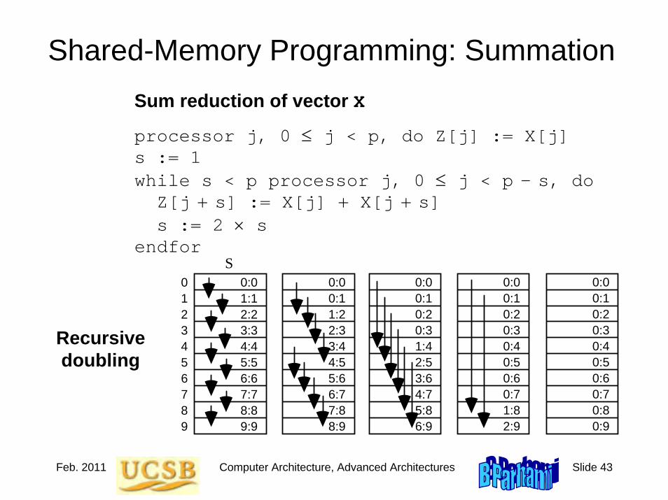
Feb. 2011 Computer Architecture, Advanced Architectures Slide 43
Shared-Memory Programming: SummationSum reduction of vector X
processor j, 0 ≤ j < p, do Z[j] := X[j]s := 1while s < p processor j, 0 ≤ j < p – s, do
Z[j + s] := X[j] + X[j + s]s := 2 × s
endfor
0 1 2 3 4 5 6 7 8 9
S 0:0 1:1 2:2 3:3 4:4 5:5 6:6 7:7 8:8 9:9
0:0 0:1 1:2 2:3 3:4 4:5 5:6 6:7 7:8 8:9
0:0 0:1 0:2 0:3 1:4 2:5 3:6 4:7 5:8 6:9
0:0 0:1 0:2 0:3 0:4 0:5 0:6 0:7 1:8 2:9
0:0 0:1 0:2 0:3 0:4 0:5 0:6 0:7 0:8 0:9
Recursivedoubling

Feb. 2011 Computer Architecture, Advanced Architectures Slide 44
27.2 Multiple Caches and Cache Coherence
Private processor caches reduce memory access traffic through the interconnection network but lead to challenging consistency problems.
0 0
1 1
m−1
Processor-to-
memory network
p−1
Processor-to-
processor network
Processors Caches Memory modules
Parallel I/O
. . .
.
.
.
.
.
.

Feb. 2011 Computer Architecture, Advanced Architectures Slide 45
Status of Data Copies
Figure 27.4 Various types of cached data blocks in a parallel processor with centralized main memory and private processor caches.
0
1
Processor-to-
memory network
p–1
Processor-to-
processor network
Processors Caches Memory modules
Parallel I/O
. . .
.
.
.
.
.
.
w x
y
z ′
w z ′
w y ′
x z
Multiple consistent
Single consistent
Single inconsistent
Invalid
m–1
0
1
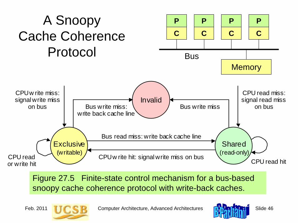
Feb. 2011 Computer Architecture, Advanced Architectures Slide 46
A Snoopy Cache Coherence
Protocol
Figure 27.5 Finite-state control mechanism for a bus-based snoopy cache coherence protocol with write-back caches.
CPU read or write hit
Invalid
Shared (read-only)
Exclusive (writable)
CPU read hit
CPU read miss: signal read miss
on bus
CPU w rite miss: signal write miss
on bus
CPU w rite hit: signal write miss on bus
Bus write miss: write back cache line
Bus write miss
Bus read miss: write back cache line
PC
PC
PC
PC
BusMemory

Feb. 2011 Computer Architecture, Advanced Architectures Slide 47
27.3 Implementing Symmetric Multiprocessors
Figure 27.6 Structure of a generic bus-based symmetric multiprocessor.
Computing nodes (typically, 1-4 CPUs
and caches per node)
Interleaved memory
Bus adapter
I/O modules
Standard interfaces
Bus adapter
Very wide, high-bandwidth bus
Feb. 2011 Computer Architecture, Advanced Architectures Slide 48
Bus Bandwidth Limits PerformanceExample 27.1
Consider a shared-memory multiprocessor built around a single bus with a data bandwidth of x GB/s. Instructions and data words are 4 B wide, each instruction requires access to an average of 1.4 memory words (including the instruction itself). The combined hit rate for caches is 98%. Compute an upper bound on the multiprocessor performance in GIPS. Address lines are separate and do not affect the bus data bandwidth.
Solution
Executing an instruction implies a bus transfer of 1.4 × 0.02 × 4 = 0.112B. Thus, an absolute upper bound on performance is x/0.112 = 8.93x GIPS. Assuming a bus width of 32 B, no bus cycle or data going to waste, and a bus clock rate of y GHz, the performance bound becomes 286y GIPS. This bound is highly optimistic. Buses operate in the range 0.1 to 1 GHz. Thus, a performance level approaching 1 TIPS (perhaps even ¼ TIPS) is beyond reach with this type of architecture.

Feb. 2011 Computer Architecture, Advanced Architectures Slide 49
Implementing Snoopy Caches
Figure 27.7 Main structure for a snoop-based cache coherence algorithm.
Tags
Cache data array
Duplicate tags and state store for snoop side
CPU
Main tags and state store for processor side
=?
=?
Processor side cache control
Snoop side cache control
Addr Addr Cmd Cmd Buffer Buffer Snoop state
System bus
Tag
Addr Cmd
State

Feb. 2011 Computer Architecture, Advanced Architectures Slide 50
27.4 Distributed Shared Memory
Figure 27.8 Structure of a distributed shared-memory multiprocessor.
0
1 z : 0
x : 0 y : 1
Inter- connection
network
Processors with memory
Par
alle
l inp
ut/o
utpu
t
. . .
p−1
y := -1 z := 1
while z=0 do x := x + y endwhile
Routers

Feb. 2011 Computer Architecture, Advanced Architectures Slide 51
27.5 Directories to Guide Data Access
Figure 27.9 Distributed shared-memory multiprocessor with a cache, directory, and memory module associated with each processor.
0
1
Inter- connection
network
Processors & caches
Par
alle
l inp
ut/o
utpu
t
. . .
p−1
Memories
Directories Communication & memory interfaces

Feb. 2011 Computer Architecture, Advanced Architectures Slide 52
Directory-Based Cache Coherence
Figure 27.10 States and transitions for a directory entry in a directory-based cache coherence protocol (c is the requesting cache).
Write miss: return value, set sharing set to {c}
Uncached
Shared (read-only)
Exclusive (writable)
Read miss: return value, include c in sharing set
Read miss: return value, set sharing set to {c}
Write miss: invalidate all cached copies, set sharing set to {c}, return value
Data w rite-back: set sharing set to { }
Read miss: fetch data from owner, return value, include c in sharing set
Write miss: fetch data from owner, request invalidation,
return value, set sharing set to {c}

Feb. 2011 Computer Architecture, Advanced Architectures Slide 53
27.6 Implementing Asymmetric Multiprocessors
Figure 27.11 Structure of a ring-based distributed-memory multiprocessor.
Computing nodes (typically, 1-4 CPUs and associated memory)
Link
To I/O controllers
Memory
Ring network
Link Link Link
Node 0 Node 1 Node 2 Node 3

Feb. 2011 Computer Architecture, Advanced Architectures Slide 54
Scalable Coherent Interface
(SCI)
Figure 27.11 Structure of a ring-based distributed-memory multiprocessor.
0
1
Processors and caches
To in
terc
onne
ctio
n ne
twor
k
3
Memories
2

Feb. 2011 Computer Architecture, Advanced Architectures Slide 55
28 Distributed MulticomputingComputer architects’ dream: connect computers like toy blocks
• Building multicomputers from loosely connected nodes• Internode communication is done via message passing
Topics in This Chapter28.1 Communication by Message Passing
28.2 Interconnection Networks
28.3 Message Composition and Routing
28.4 Building and Using Multicomputers
28.5 Network-Based Distributed Computing
28.6 Grid Computing and Beyond

Feb. 2011 Computer Architecture, Advanced Architectures Slide 56
28.1 Communication by Message Passing
Figure 28.1 Structure of a distributed multicomputer.
0
1
Inter- connection
network
Memories and processors
Par
alle
l inp
ut/o
utpu
t
p−1
. . .
Routers
A computing node

Feb. 2011 Computer Architecture, Advanced Architectures Slide 57
Router Design
Figure 28.2 The structure of a generic router.
Switch
Inpu
t cha
nnel
s
Routing and arbitration
Input queues
Q
Q
Q
Q
Q
Q
Q
Q
LC
LC
LC
LC
LC
LC
LC
LC Out
put c
hann
els
Output queues
Q Q
LC LC Link controller
Message queue
Injection channel Ejection channel

Feb. 2011 Computer Architecture, Advanced Architectures Slide 58
Building Networks from Switches
Straight through Crossed connection Lower broadcast Upper broadcast
Figure 28.3 Example 2 × 2 switch with point-to-point and broadcast connection capabilities.
(a) Butterfly network (b) Beneš network
0
2
4
6
8
10
12
14
Processors Memories
P r o c e s s o r s
M e m o r i e s
1
3
5
7
9
11
13
15
0
2
4
6
8
10
12
14
1
3
5
7
9
11
13
15
0
2
4
6
0
2
4
6
1
3
5
7
1
3
5
7
Row 0
Row 1
Row 2
Row 3
Row 4
Row 5
Row 6
Row 7
Figure 27.2Butterfly and Beneš networks
Feb. 2011 Computer Architecture, Advanced Architectures Slide 59
Interprocess Communication via Messages
Figure 28.4 Use of send and receive message-passing primitives to synchronize two processes.
Process A Process B
...
...
...
...
...
... send x ... ... ... ... ... ... ...
...
... receive x ... ... ... Time
Communication latency
Process B is suspended
Process B is awakened

Feb. 2011 Computer Architecture, Advanced Architectures Slide 60
28.2 Interconnection Networks
Figure 28.5 Examples of direct and indirect interconnection networks.
(a) Direct network (b) Indirect network
Routers Nodes Nodes
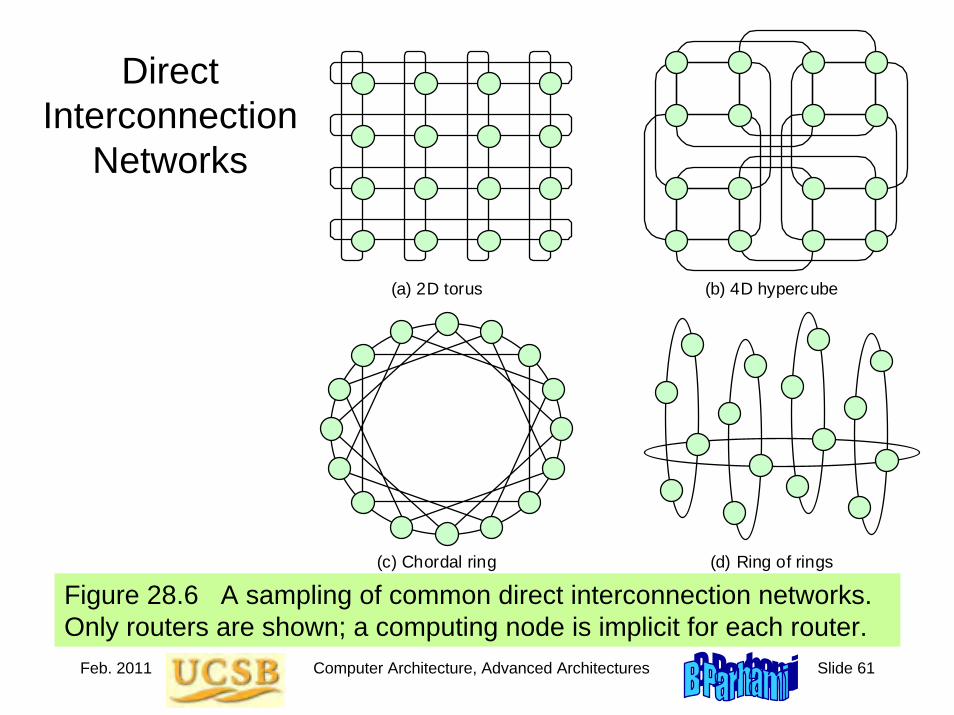
Feb. 2011 Computer Architecture, Advanced Architectures Slide 61
Direct Interconnection
Networks
Figure 28.6 A sampling of common direct interconnection networks. Only routers are shown; a computing node is implicit for each router.
(a) 2D torus (b) 4D hypercube
(c) Chordal ring (d) Ring of rings
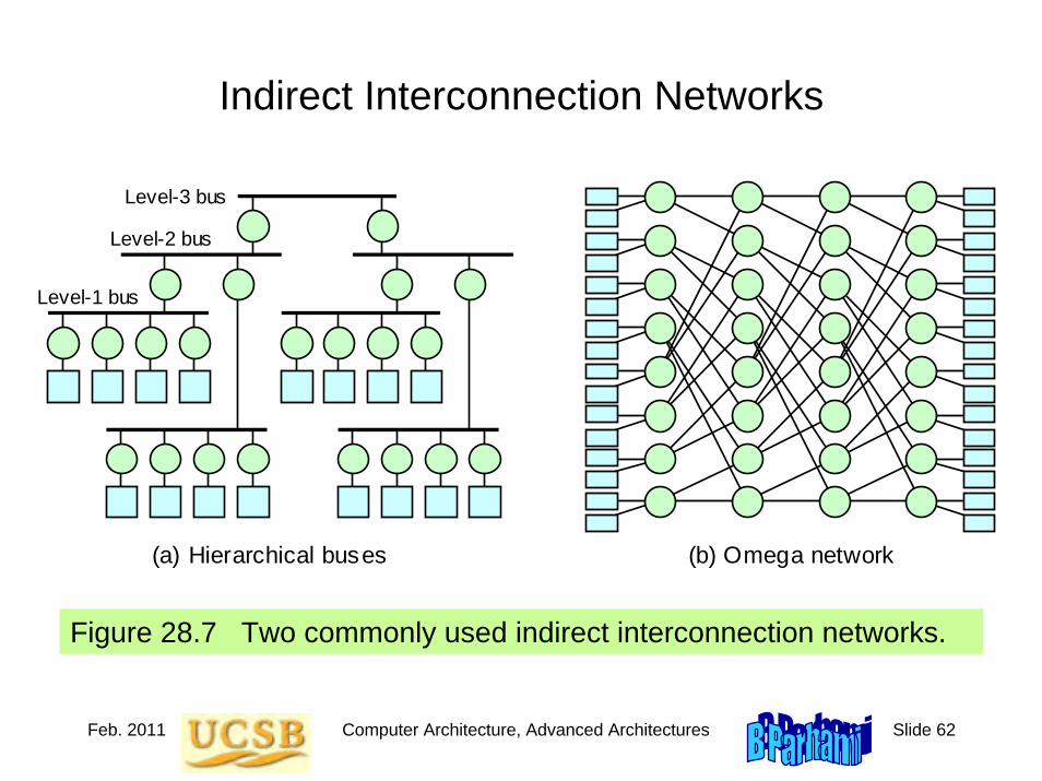
Feb. 2011 Computer Architecture, Advanced Architectures Slide 62
Indirect Interconnection Networks
Figure 28.7 Two commonly used indirect interconnection networks.
(a) Hierarchical buses (b) Omega network
Level-1 bus
Level-2 bus
Level-3 bus

Feb. 2011 Computer Architecture, Advanced Architectures Slide 63
28.3 Message Composition and Routing
Figure 28.8 Messages and their parts for message passing.
Message Padding
Packet data
Last packet Header Trailer
A transmitted packet
Flow control digits (flits)
Data or payload First packet

Feb. 2011 Computer Architecture, Advanced Architectures Slide 64
Wormhole Switching
Figure 28.9 Concepts of wormhole switching.
Worm 1: moving
(a) Two worms en route to their respective destinations
Source 2
Source 1
Destination 1
Destination 2
Worm 2: blocked
(b) Deadlock due to circular waiting of four blocked worms
Each worm is blocked at the point of attempted right turn

Feb. 2011 Computer Architecture, Advanced Architectures Slide 65
28.4 Building and Using Multicomputers
Figure 28.10 A task system and schedules on 1, 2, and 3 computers.
(a) Static task graph (b) Schedules on 1-3 computers
Inputs
Outputs
t = 1
t = 1
t = 2
t = 2 t = 2
t = 3
B
A C
D
E
F
G
H
t = 1
t = 2
B A C D E F G H
B A C
D E
H F G
B A C
D
E F G H
0 5 10 15
Time

Feb. 2011 Computer Architecture, Advanced Architectures Slide 66
Building Multicomputers from Commodity Nodes
Figure 28.11 Growing clusters using modular nodes.
(a) Current racks of modules (b) Futuristic toy-block construction
Expansion slots
One module: CPU,
memory, disks
One module:CPU(s), memory,
disks
Wireless connection surfaces

Feb. 2011 Computer Architecture, Advanced Architectures Slide 67
28.5 Network-Based Distributed Computing
Figure 28.12 Network of workstations.
System or I/O bus PC
Fast network interface with large memory
NIC
Network built of high-speed
wormhole switches

Feb. 2011 Computer Architecture, Advanced Architectures Slide 68
28.6 Grid Computing and Beyond
Computational grid is analogous to the power grid
Decouples the “production” and “consumption” of computational power
Homes don’t have an electricity generator; why should they have a computer?
Advantages of computational grid:
Near continuous availability of computational and related resourcesResource requirements based on sum of averages, rather than sum of peaksPaying for services based on actual usage rather than peak demandDistributed data storage for higher reliability, availability, and securityUniversal access to specialized and one-of-a-kind computing resources
Still to be worked out as of late 2000s: How to charge for compute usage
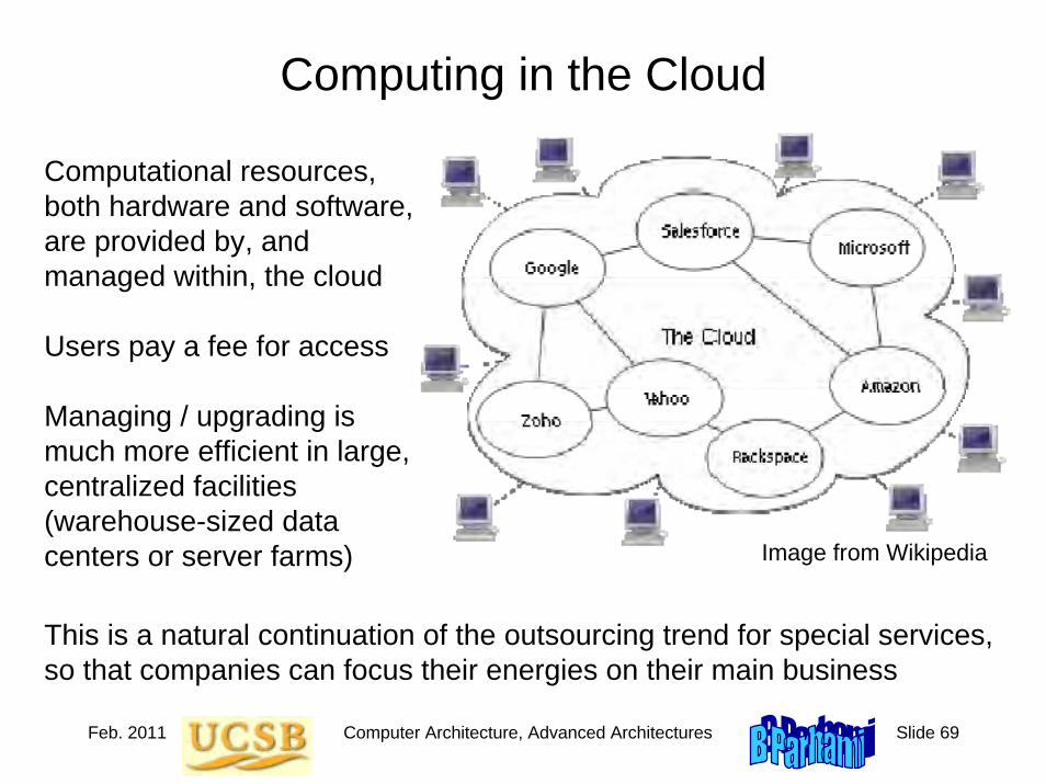
Feb. 2011 Computer Architecture, Advanced Architectures Slide 69
Computing in the Cloud
Image from Wikipedia
Computational resources,both hardware and software,are provided by, and managed within, the cloud
Users pay a fee for access
Managing / upgrading is much more efficient in large, centralized facilities (warehouse-sized data centers or server farms)
This is a natural continuation of the outsourcing trend for special services, so that companies can focus their energies on their main business
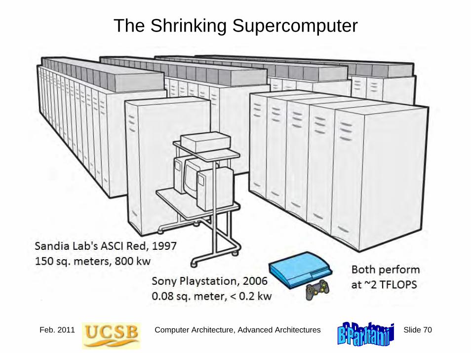
Feb. 2011 Computer Architecture, Advanced Architectures Slide 70
The Shrinking Supercomputer

Feb. 2011 Computer Architecture, Advanced Architectures Slide 71
Warehouse-Sized Data Centers
Image from IEEE Spectrum, June 2009


![Feb 25, 2009 Lecture 5-1 instruction set architecture (Part II of [Parhami]) subroutines and functions implementing recursion – example more examples of](https://img.pdfslide.us/doc/110x75/56649d6a5503460f94a49259/feb-25-2009-lecture-5-1-instruction-set-architecture-part-ii-of-parhami.jpg)