Embed Size (px)
Citation preview
Computer Aided Design (CAD)
Lecture 13
Dr.Eng. Basem ElHalawany
Introduction to FPGA
2
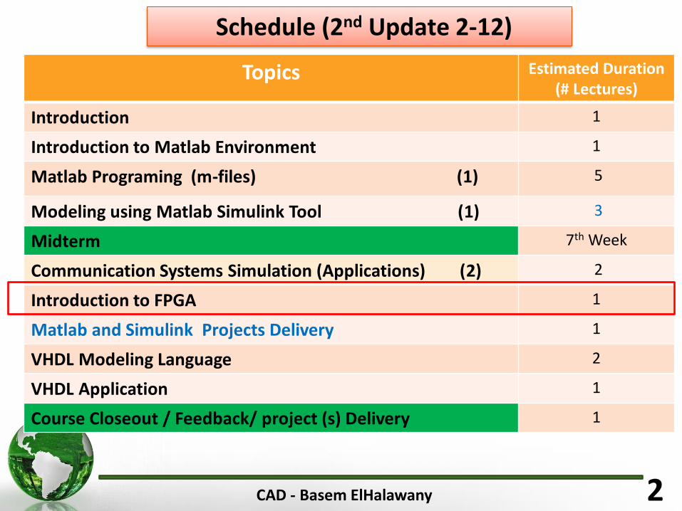
Schedule (2nd Update 2-12)
CAD - Basem ElHalawany
Topics Estimated Duration (# Lectures)
Introduction 1
Introduction to Matlab Environment 1
Matlab Programing (m-files) (1) 5
Modeling using Matlab Simulink Tool (1) 3
Midterm 7th Week
Communication Systems Simulation (Applications) (2) 2
Introduction to FPGA 1
Matlab and Simulink Projects Delivery 1
VHDL Modeling Language 2
VHDL Application 1
Course Closeout / Feedback/ project (s) Delivery 1
3
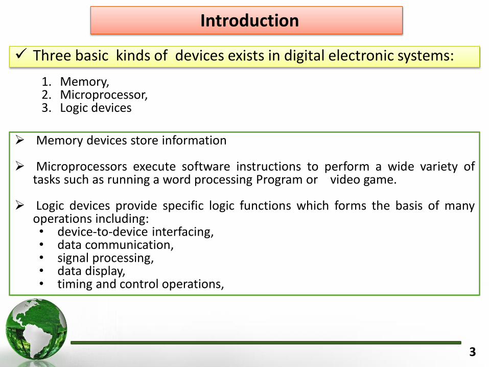
Memory devices store information
Microprocessors execute software instructions to perform a wide variety of tasks such as running a word processing Program or video game.
Logic devices provide specific logic functions which forms the basis of many operations including: • device-to-device interfacing, • data communication, • signal processing, • data display, • timing and control operations,
Introduction
Three basic kinds of devices exists in digital electronic systems:
1. Memory, 2. Microprocessor, 3. Logic devices

CAD – Dr.Eng. Basem ElHalawany 4
Logic Devices
A logic device is one which can perform any logic function Logic devices are broadly classified into:
For Academic Use Only Presentation Name
4
Logic
Standard Logic
ASIC
Programmable Logic Devices
(PLDs)
GAL Cell-Based ICs
Full Custom ICs
CPLDs SPLDs (PALs) FPGAs
• ASIC = Application-Specific IC
• SPLD = Simple Programmable Logic Devices (PLD)
• PAL = Programmable Array of Logic
• CPLD = Complex PLD
• GAL = Gate Array logic
• FPGA = Field Programmable Gate Array
CAD – Dr.Eng. Basem ElHalawany 5
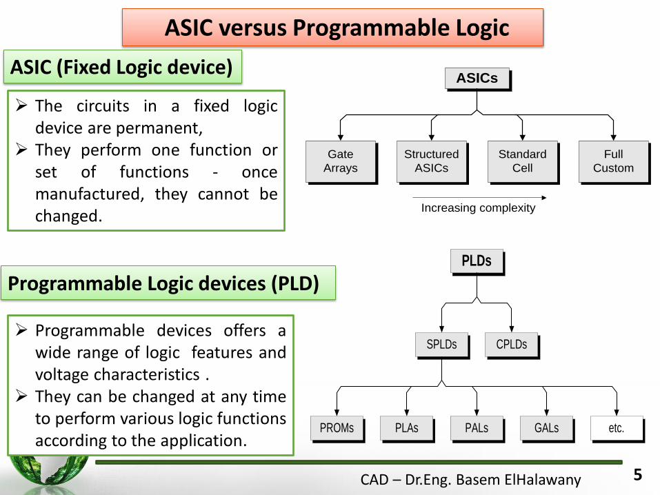
The circuits in a fixed logic device are permanent,
They perform one function or set of functions - once manufactured, they cannot be changed.
ASIC versus Programmable Logic
Programmable devices offers a wide range of logic features and voltage characteristics .
They can be changed at any time to perform various logic functions according to the application.
ASIC (Fixed Logic device)
Programmable Logic devices (PLD)
ASICs
Structured
ASICs
Gate
Arrays
Standard
Cell
Full
Custom
Increasing complexity
PLDs
SPLDs CPLDs
PLAsPROMs PALs GALs etc.
6
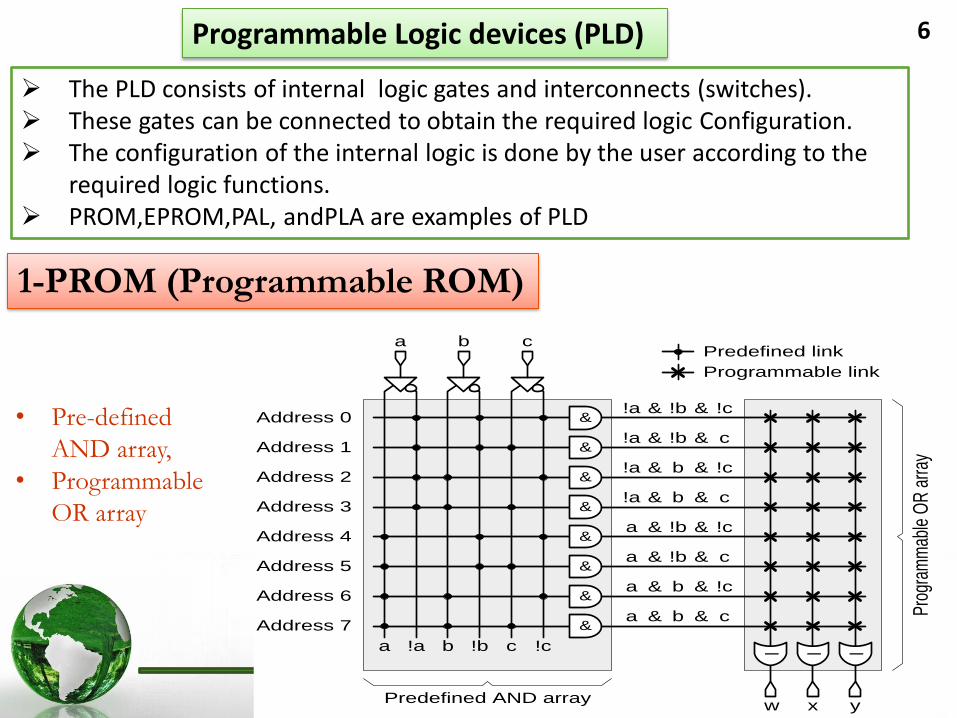
The PLD consists of internal logic gates and interconnects (switches). These gates can be connected to obtain the required logic Configuration. The configuration of the internal logic is done by the user according to the
required logic functions. PROM,EPROM,PAL, andPLA are examples of PLD
Programmable Logic devices (PLD)
a b c
l l l
Address 0 &
Address 1 &
Address 2 &
Address 3 &
Address 4 &
Address 5 &
Address 6 &
Address 7 &
a !a b !b c !c
!a !c!b& &
!a c!b& &
!a !cb& &
!a cb& &
a !c!b& &
a c!b& &
a !cb& &
a cb& &
Predefined AND array
Prog
ram
mab
le O
R a
rray
w x y
Predefined link
Programmable link
1-PROM (Programmable ROM)
• Pre-defined
AND array,
• Programmable
OR array

CAD – Dr.Eng. Basem ElHalawany 7
1-PROM (Programmable ROM)
a b c
l l lAddress 0 &
Address 1 &
Address 2 &
Address 3 &
Address 4 &
Address 5 &
Address 6 &
Address 7 &
a !a b !b c !c
!a !c!b& &
!a c!b& &
!a !cb& &
!a cb& &
a !c!b& &
a c!b& &
a !cb& &
a cb& &
Predefined AND array
Pro
gram
mab
le O
R a
rray
w x y
Predefined link
Programmable link
w = (a & b)
x = !(a & b)
y = (a & b) ^ c
CAD – Dr.Eng. Basem ElHalawany 8
a b c
&
&
&
a !a b !b c !c
N/A
Predefined AND array
Pro
gram
mab
le
OR
arr
ay
Predefined link
Programmable link
l l l
w x y
N/A
N/A
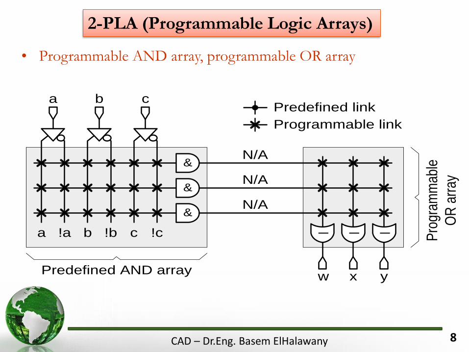
2-PLA (Programmable Logic Arrays)
• Programmable AND array, programmable OR array
CAD – Dr.Eng. Basem ElHalawany 9
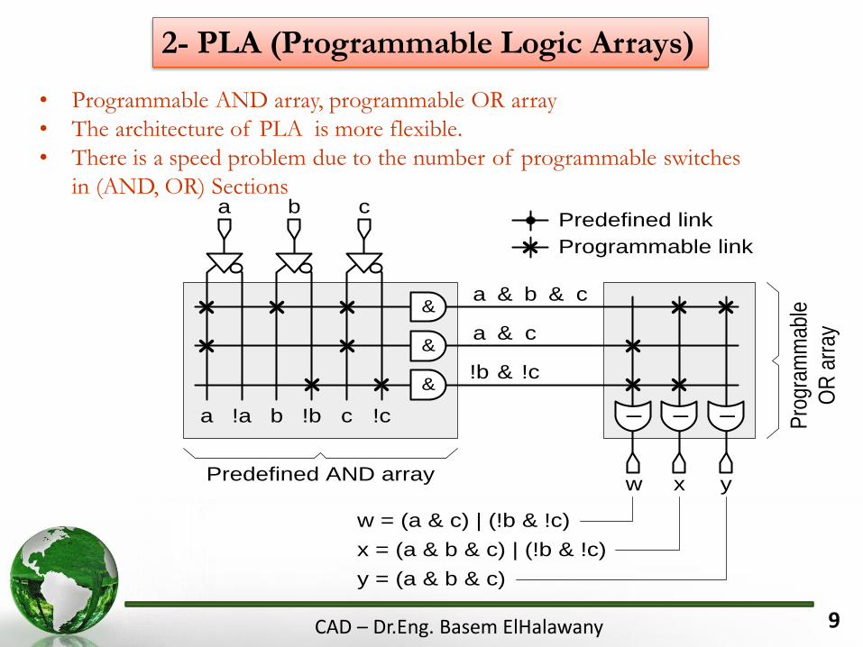
2- PLA (Programmable Logic Arrays)
• Programmable AND array, programmable OR array
• The architecture of PLA is more flexible.
• There is a speed problem due to the number of programmable switches
in (AND, OR) Sections a b c
&
&
&
a !a b !b c !c
a cb& &
a c&
!b !c&
Predefined AND array
Pro
gram
mab
le
OR
arr
ay
Predefined link
Programmable linkl l l
w x y
w = (a & c) | (!b & !c)
x = (a & b & c) | (!b & !c)
y = (a & b & c)
10
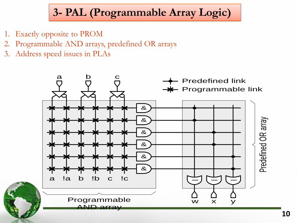
3- PAL (Programmable Array Logic)
1. Exactly opposite to PROM
2. Programmable AND arrays, predefined OR arrays
3. Address speed issues in PLAs
a b c
l l l
&
&
&
&
&
&
a !a b !b c !c
Programmable
AND array
Pred
efin
ed O
R ar
ray
w x y
Predefined link
Programmable link
11
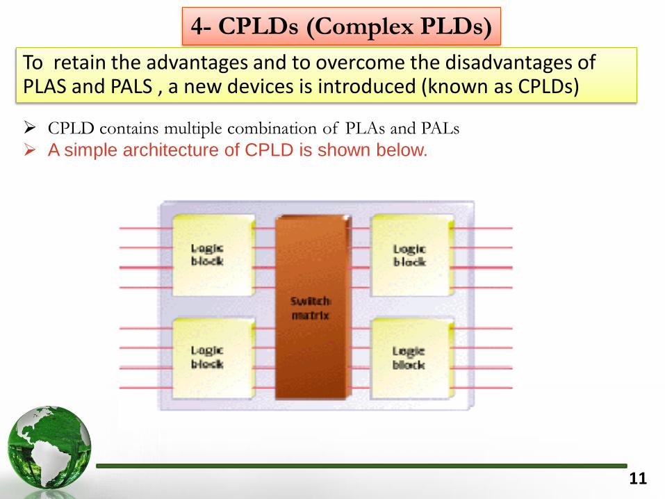
4- CPLDs (Complex PLDs)
CPLD contains multiple combination of PLAs and PALs
A simple architecture of CPLD is shown below.
To retain the advantages and to overcome the disadvantages of PLAS and PALS , a new devices is introduced (known as CPLDs)
12
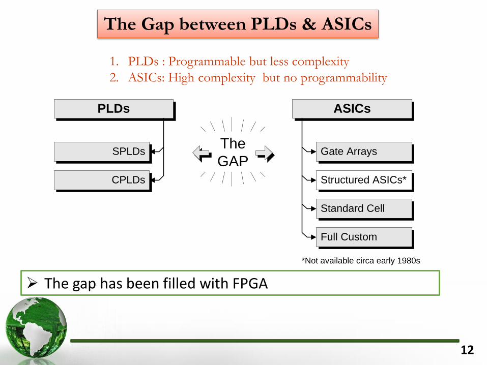
The Gap between PLDs & ASICs
The gap has been filled with FPGA
1. PLDs : Programmable but less complexity
2. ASICs: High complexity but no programmability
PLDs ASICs
Standard Cell
Full Custom
Gate Arrays
Structured ASICs*
SPLDs
CPLDs
*Not available circa early 1980s
The
GAP

13
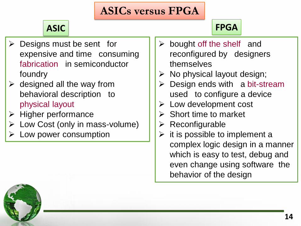
ASICs versus FPGA)
Manufacturing cycle for ASIC is very costly, lengthy and engages lots of manpower in fabrication.
Mistakes not detected at design time have large impact on development time and cost of ASIC
FPGAs are re-programmable chips, which is perfect for rapid prototyping of digital circuits.
Easy upgrades like in case of software applications in FPGA
14
ASICs versus FPGA
Designs must be sent for
expensive and time consuming
fabrication in semiconductor
foundry
designed all the way from
behavioral description to
physical layout
Higher performance
Low Cost (only in mass-volume)
Low power consumption
ASIC
bought off the shelf and
reconfigured by designers
themselves
No physical layout design;
Design ends with a bit-stream
used to configure a device
Low development cost
Short time to market
Reconfigurable
it is possible to implement a
complex logic design in a manner
which is easy to test, debug and
even change using software the
behavior of the design
FPGA
15
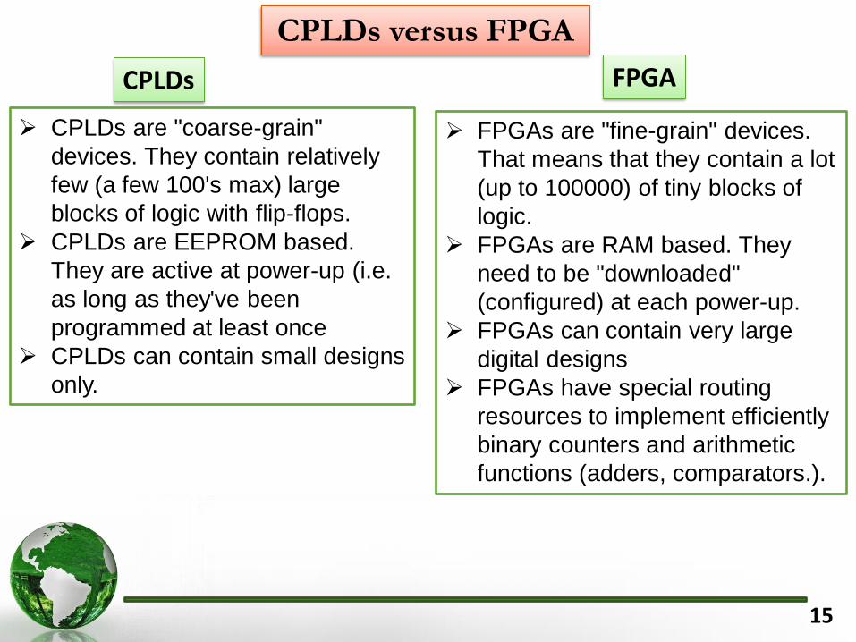
CPLDs versus FPGA
FPGAs are "fine-grain" devices.
That means that they contain a lot
(up to 100000) of tiny blocks of
logic.
FPGAs are RAM based. They
need to be "downloaded"
(configured) at each power-up.
FPGAs can contain very large
digital designs
FPGAs have special routing
resources to implement efficiently
binary counters and arithmetic
functions (adders, comparators.).
CPLDs
CPLDs are "coarse-grain"
devices. They contain relatively
few (a few 100's max) large
blocks of logic with flip-flops.
CPLDs are EEPROM based.
They are active at power-up (i.e.
as long as they've been
programmed at least once
CPLDs can contain small designs
only.
FPGA
16
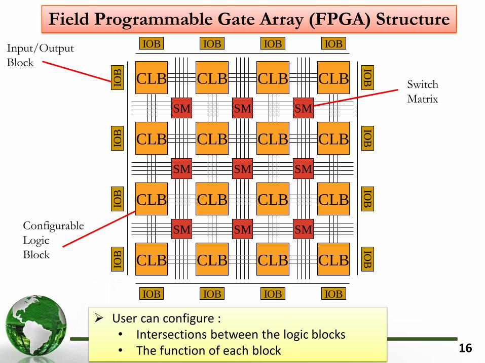
Field Programmable Gate Array (FPGA) Structure
CLB CLB
CLB CLB
SM SM
SM SM
CLB CLB
CLB CLB
SM
SM
CLB CLB
CLB CLB
SM SM
CLB CLB
CLB CLB
SM
IOB IOB IOB IOB
IOB IOB IOB IOB
IOB
IO
B
IOB
IO
B
IOB
IO
B
IOB
IO
B
Input/Output
Block
Switch
Matrix
Configurable
Logic
Block
User can configure : • Intersections between the logic blocks • The function of each block
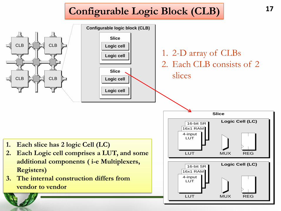
17 Configurable Logic Block (CLB)
CLB CLB
CLB CLB
Logic cell
Slice
Logic cell
Logic cell
Slice
Logic cell
Configurable logic block (CLB)
1. 2-D array of CLBs
2. Each CLB consists of 2
slices
16-bit SR
16x1 RAM
4-input
LUT
LUT MUX REG
Logic Cell (LC)
16-bit SR
16x1 RAM
4-input
LUT
LUT MUX REG
Logic Cell (LC)
Slice
1. Each slice has 2 logic Cell (LC)
2. Each Logic cell comprises a LUT, and some
additional components ( i-e Multiplexers,
Registers)
3. The internal construction differs from
vendor to vendor

18
Major FPGA Vendors
19
FPGA Design and Programming
To define the behavior of the FPGA the user provides a hardware description language (HDL) or a schematic design.
Then, using an electronic design automation tool, a technology-mapped net list is generated.
The netlist can then be fitted to the actual FPGA architecture using a process called place-and-route.
The user will validate the map, place and route results via timing analysis, simulation, and other verification methodologies.
Once the design and validation process is complete, the binary file generated used to configure the FPGA.
20
• Verilog
HDL Languages
• VHDL