Embed Size (px)
Citation preview
Electronic Component Zero Orientation
For CAD Library Construction
3000 Lakside Drive Suite 309S Bannockburn, IL, 60015 Tel: 847-615-7100 Fax: 847-615-7105 www.ipc.org
PCB Libraries, Inc. 701 Lee Street Des Plaines, IL 60016 Tel: 877-722-4441 Fax: 847.745.0450 www.PCBLibraries.com
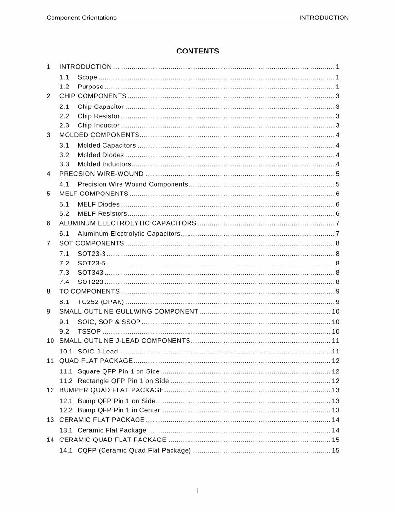
Component Orientations INTRODUCTION
i
CONTENTS 1 INTRODUCTION ............................................................................................................ 1
1.1 Scope ................................................................................................................... 1 1.2 Purpose ................................................................................................................ 1
2 CHIP COMPONENTS ..................................................................................................... 3 2.1 Chip Capacitor ...................................................................................................... 3 2.2 Chip Resistor ........................................................................................................ 3 2.3 Chip Inductor ........................................................................................................ 3
3 MOLDED COMPONENTS............................................................................................... 4 3.1 Molded Capacitors ................................................................................................ 4 3.2 Molded Diodes ...................................................................................................... 4 3.3 Molded Inductors................................................................................................... 4
4 PRECSION WIRE-WOUND ............................................................................................ 5 4.1 Precision Wire Wound Components ....................................................................... 5
5 MELF COMPONENTS .................................................................................................... 6 5.1 MELF Diodes ........................................................................................................ 6 5.2 MELF Resistors..................................................................................................... 6
6 ALUMINUM ELECTROLYTIC CAPACITORS ................................................................... 7 6.1 Aluminum Electrolytic Capacitors........................................................................... 7
7 SOT COMPONENTS ...................................................................................................... 8 7.1 SOT23-3 ............................................................................................................... 8 7.2 SOT23-5 ............................................................................................................... 8 7.3 SOT343 ................................................................................................................ 8 7.4 SOT223 ................................................................................................................ 8
8 TO COMPONENTS ........................................................................................................ 9 8.1 TO252 (DPAK) ...................................................................................................... 9
9 SMALL OUTLINE GULLWING COMPONENT ................................................................ 10 9.1 SOIC, SOP & SSOP ............................................................................................ 10 9.2 TSSOP ............................................................................................................... 10
10 SMALL OUTLINE J-LEAD COMPONENTS.................................................................... 11 10.1 SOIC J-Lead ....................................................................................................... 11
11 QUAD FLAT PACKAGE................................................................................................ 12 11.1 Square QFP Pin 1 on Side................................................................................... 12 11.2 Rectangle QFP Pin 1 on Side .............................................................................. 12
12 BUMPER QUAD FLAT PACKAGE................................................................................. 13 12.1 Bump QFP Pin 1 on Side ..................................................................................... 13 12.2 Bump QFP Pin 1 in Center .................................................................................. 13
13 CERAMIC FLAT PACKAGE .......................................................................................... 14 13.1 Ceramic Flat Package ......................................................................................... 14
14 CERAMIC QUAD FLAT PACKAGE ............................................................................... 15 14.1 CQFP (Ceramic Quad Flat Package) ................................................................... 15
Component Orientations INTRODUCTION
ii
15 PLASTIC LEADED CHIP CARRIERS ............................................................................ 16 15.1 PLCC Square ...................................................................................................... 16 15.2 PLCC Rectangular .............................................................................................. 16
16 LEADLESS CHIP CARRIERS ....................................................................................... 17 16.1 LCC Square ........................................................................................................ 17 16.2 Chip Array........................................................................................................... 17
17 QUAD FLAT NO-LEAD ................................................................................................. 18 17.1 QFN Square ........................................................................................................ 18 17.2 QFN Rectangular Vertical .................................................................................... 18 17.3 QFN Rectangular Horizontal ................................................................................ 18
18 BALL GRID ARRAY...................................................................................................... 19 18.1 BGA Square ........................................................................................................ 19 18.2 BGA Rectangular ................................................................................................ 19
19 COMPONENT ZERO ORIENTATIONS.......................................................................... 20 19.1 Summary ............................................................................................................ 20
20 APPENDIX A - EIA Survey for Component Orientation ................................................ 21 20.1 Purpose .............................................................................................................. 21 20.2 Driving factors ..................................................................................................... 21 20.3 Examples of Possible Conflict.............................................................................. 22 20.4 Recommendation ................................................................................................ 24 20.5 Presentation of Results ....................................................................................... 28
21 APPENDIX B – Internet Search Results ........................................................................ 29 21.1 Device Orientation (Catalyst) ............................................................................... 29 21.2 Device Orientation (LRC China)........................................................................... 29 21.3 Device Orientation (Diodes, Incorporated)............................................................ 30 21.4 Device Orientation (Fairchild Semiconductor)....................................................... 31 21.5 Device Orientation (Linear Technology) ............................................................... 31 21.6 Device Orientation (RF Technologies).................................................................. 34 21.7 Device Orientation (Microchip Devices)................................................................ 36 21.8 Device Orientation (ZETEX) ................................................................................ 40 21.9 Device Orientation (IDT) ...................................................................................... 41
22 APPENDIX C – Comment Form .................................................................................... 43 23 CREDITS ..................................................................................................................... 44
23.1 Contributions....................................................................................................... 44
Component Orientations INTRODUCTION
1
1 INTRODUCTION
1.1 Scope To establish a consistent technique for the description of electronic component orientation, and their land pattern geometries, that facilitates and encourages a common data capture and transfer methodology amongst and between global trading partners.
1.2 Purpose IPC, in conjunction with the International Electrotechnical Commission (IEC), have established several standards that are in the process of being coordinated. One of the standards is on the design of land patterns geometries (IPC-7351/IEC 61188-5-1); the other set is on electronic description for data transfer between design and manufacturing (IPC-2581/IEC 61182-2). In order to maintain a consistent method where these two important standards describe the component mechanical outlines, and their respective mounting platforms, a single concept must be developed that takes into account various factors within the global community. One of these factors is that of establishing a CAD component description and land pattern standard that adopts a fixed Zero Component Orientation so that all CAD images are built with the same rotation for the purpose of assembly machine automation. The land pattern standards clearly define all the properties necessary for standardization and acceptability of a “One World CAD Library”. The main objective in defining a one world CAD library is to achieve the highest level of “Electronic Product Development Automation”. This encompasses all the processes involved from engineering to PCB layout to fabrication, assembly and test. The data format standards need this type of consistency in order to meet the efficiency that electronic data transfer can bring to the industry. Many large firms have spent millions of dollars creating and implementing their own unique standards for their own “Electronic Product Development Automation”. These standards are proprietary to each firm and are not openly shared with the rest of the industry. This has resulted in massive duplication of effort costing the industry millions of man hours in waste and creating industry chaos and global non-standardization. The industry associations responsible for component descriptions and tape and reel orientation have tried valiantly to influence the industry by making good standards that describe the component outlines and how they should be positioned in the delivery system to the equipment on the manufacturing floor (Appendix A). Suppliers of parts have either not adhered to the recommendations or have misunderstood the intent and provided their products in different orientations. (Appendix B). The Land pattern standards (both IPC-7351 and IEC 61188-5-1) put an end to the “Proprietary Intellectual Property” and introduce a world standard so every electronics firm can benefit from Electronic Product Development Automation. The data format standards (IPC-2581 and IEC 61182-2) are an open database XML software code that is neutral to all the various CAD ASCII formats. For true machine automation to exist, the world desperately needs a neutral CAD database format that all PCB manufacturing machines can read. The main purpose of creating the land pattern standards is to achieve reliable solder joint formation platforms; the reason for developing the data transfer structure is to improve the efficiency with which engineering intelligence is converted to manufacturing reality. Even if the neutral CAD format can drive all the manufacturing machines, it would be meaningless unless the component description standard for CAD land patterns was implemented with some consistency. Zero Component Orientation has a key role in machine automation.
Component Orientations INTRODUCTION
2
The obvious choice for global standardization for EE hardware engineering, PCB design layout, manufacturing, assembly and testing processes is to incorporate the standard land pattern conventions. Any other option continues the confusion and additional manual hours of intervention in order to achieve the goals of automation. In addition, the ease of having one system export a file so that another system can accomplish the work may require unnecessary manipulation of the neutral format in order to meet the object of clear, unambiguous software code. The design of any assembly will continue to permit arrangement and orientation of components at any orientation consistent with design standards. Starting from a commonly understood data capture concept will benefit the entire supply chain.
Component Orientations CHIP COMPONENTS
3
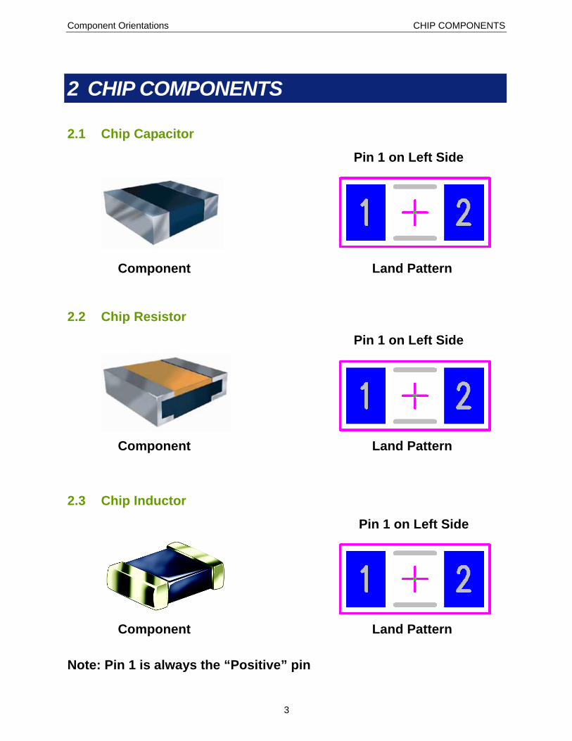
2 CHIP COMPONENTS
2.1 Chip Capacitor
Pin 1 on Left Side
Component Land Pattern
2.2 Chip Resistor
Pin 1 on Left Side
Component Land Pattern
2.3 Chip Inductor
Pin 1 on Left Side
Component Land Pattern Note: Pin 1 is always the “Positive” pin
Component Orientations MOLDED COMPONENTS
4
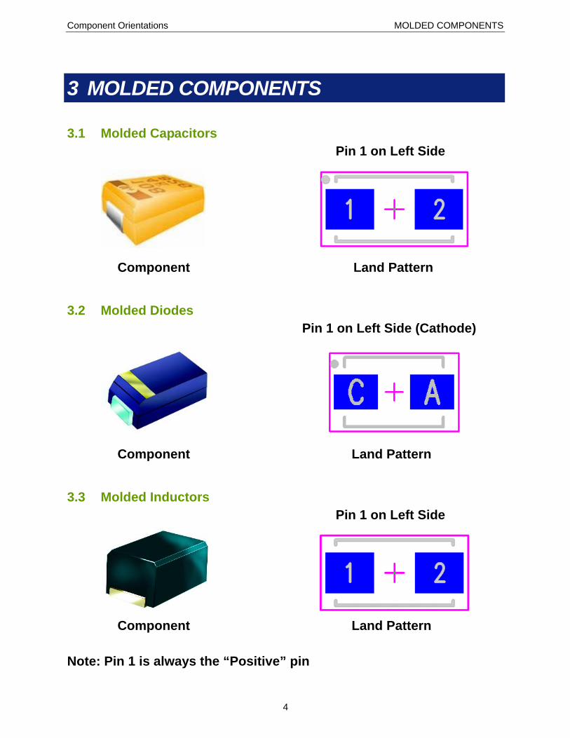
3 MOLDED COMPONENTS
3.1 Molded Capacitors Pin 1 on Left Side
Component Land Pattern
3.2 Molded Diodes Pin 1 on Left Side (Cathode)
Component Land Pattern
3.3 Molded Inductors Pin 1 on Left Side
Component Land Pattern
Note: Pin 1 is always the “Positive” pin
Component Orientations PRECSION WIRE-WOUND
5
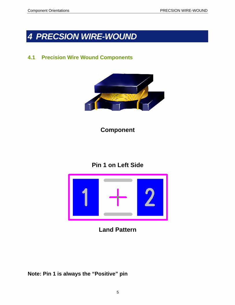
4 PRECSION WIRE-WOUND
4.1 Precision Wire Wound Components
Component
Pin 1 on Left Side
Land Pattern
Note: Pin 1 is always the “Positive” pin
Component Orientations MELF COMPONENTS
6
5 MELF COMPONENTS
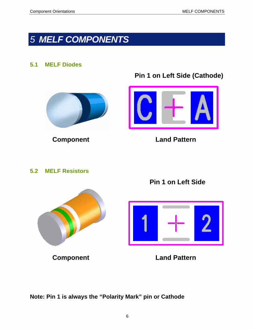
5.1 MELF Diodes
Pin 1 on Left Side (Cathode)
Component Land Pattern
5.2 MELF Resistors
Pin 1 on Left Side
Component Land Pattern
Note: Pin 1 is always the “Polarity Mark” pin or Cathode
Component Orientations ALUMINUM ELECTROLYTIC CAPACITORS
7
6 ALUMINUM ELECTROLYTIC CAPACITORS
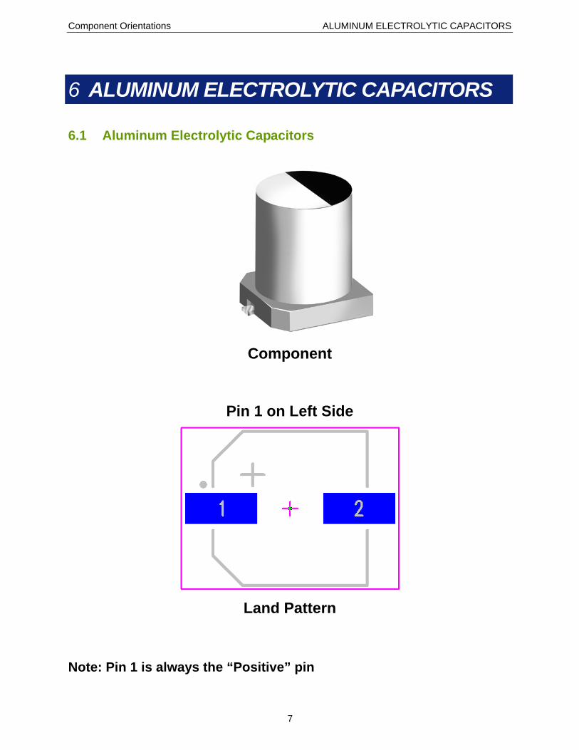
6.1 Aluminum Electrolytic Capacitors
Component
Pin 1 on Left Side
Land Pattern Note: Pin 1 is always the “Positive” pin
Component Orientations SOT COMPONENTS
8
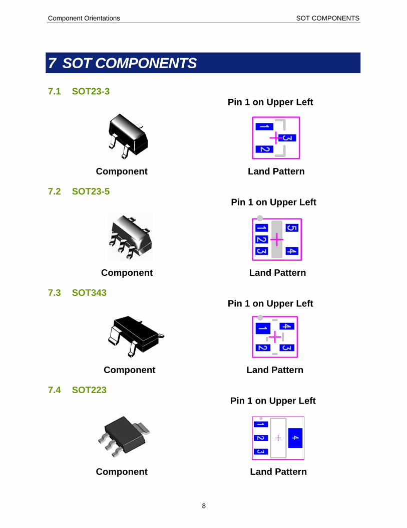
7 SOT COMPONENTS
7.1 SOT23-3 Pin 1 on Upper Left
Component Land Pattern
7.2 SOT23-5 Pin 1 on Upper Left
Component Land Pattern
7.3 SOT343 Pin 1 on Upper Left
Component Land Pattern
7.4 SOT223 Pin 1 on Upper Left
Component Land Pattern

Component Orientations TO COMPONENTS
9
8 TO COMPONENTS
8.1 TO252 (DPAK)
Component
Pin 1 on Upper Left
Land Pattern
Component Orientations SMALL OUTLINE GULLWING COMPONENT
10
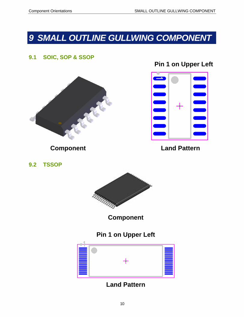
9 SMALL OUTLINE GULLWING COMPONENT
9.1 SOIC, SOP & SSOP Pin 1 on Upper Left
Component Land Pattern
9.2 TSSOP
Component
Pin 1 on Upper Left
Land Pattern
Component Orientations SMALL OUTLINE J-LEAD COMPONENTS
11
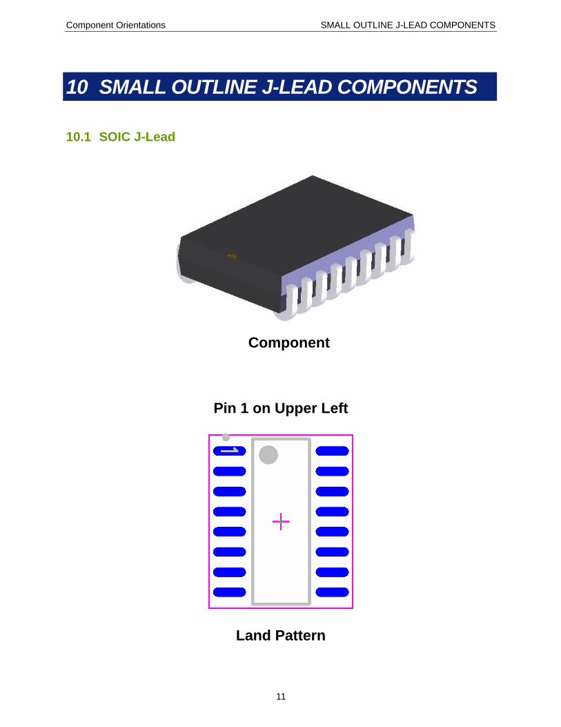
10 SMALL OUTLINE J-LEAD COMPONENTS
10.1 SOIC J-Lead
Component
Pin 1 on Upper Left
Land Pattern
IPC-7351 Component Zero Orientations QUAD FLAT PACKAGE
12
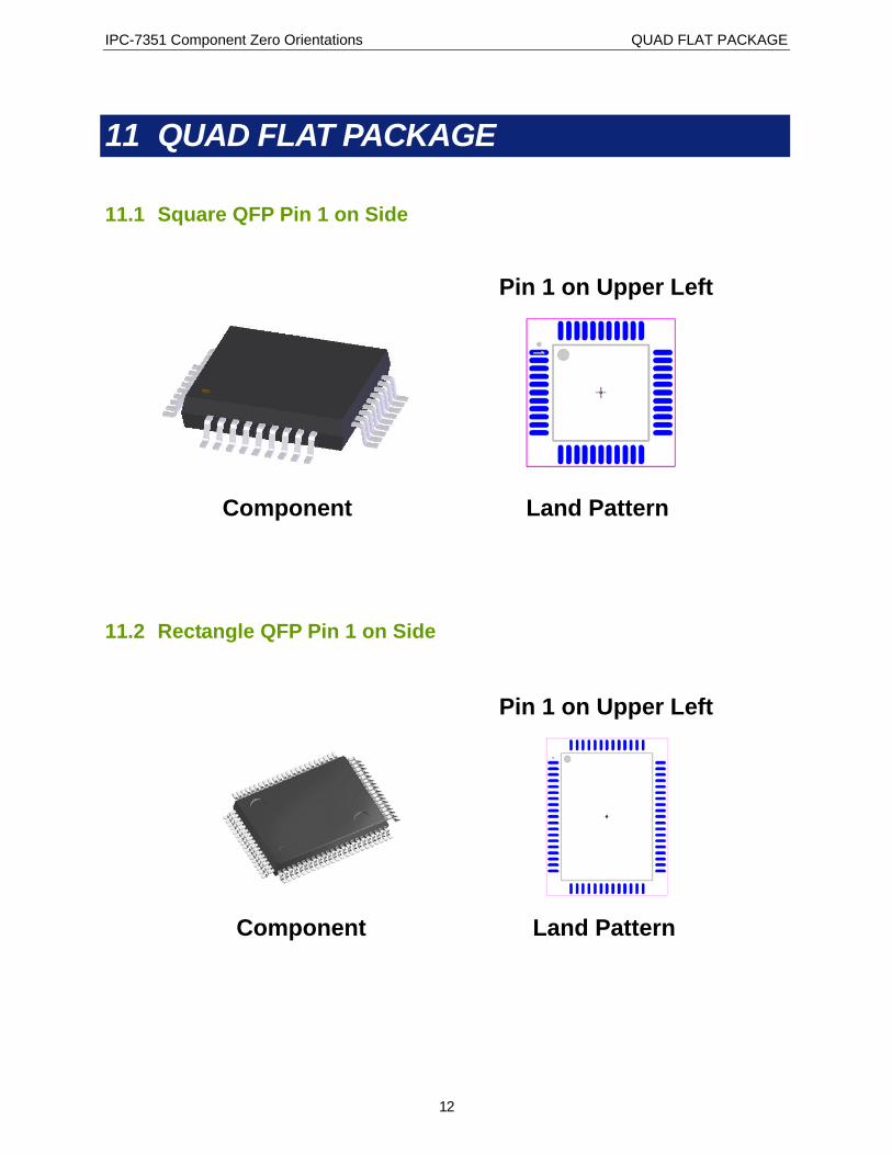
11 QUAD FLAT PACKAGE
11.1 Square QFP Pin 1 on Side
Pin 1 on Upper Left
Component Land Pattern
11.2 Rectangle QFP Pin 1 on Side
Pin 1 on Upper Left
Component Land Pattern
IPC-7351 Component Zero Orientations BUMPER QUAD FLAT PACKAGE
13
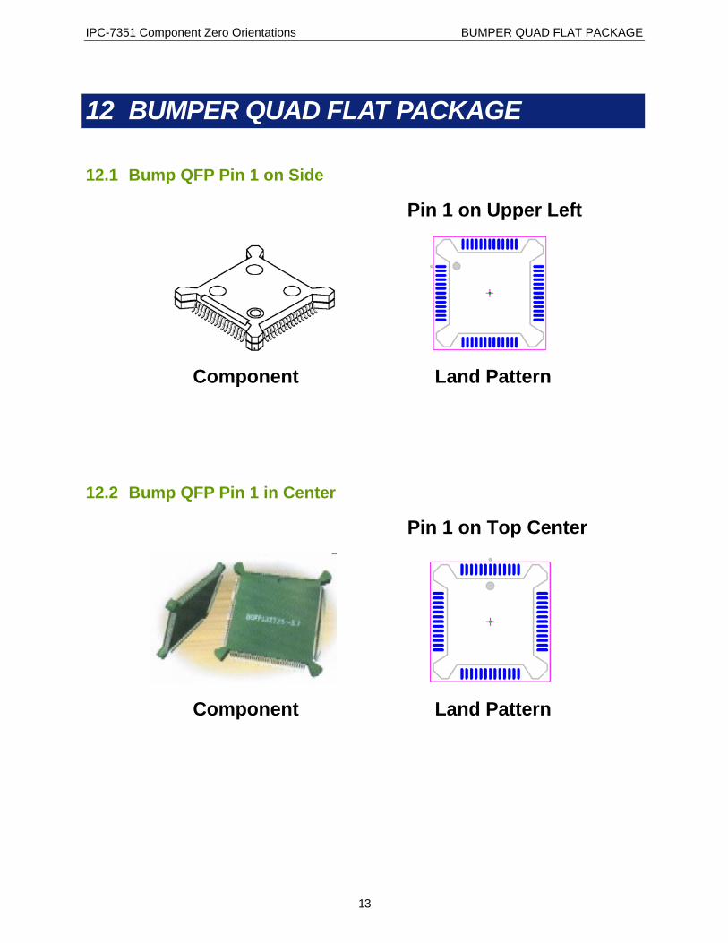
12 BUMPER QUAD FLAT PACKAGE
12.1 Bump QFP Pin 1 on Side
Pin 1 on Upper Left
Component Land Pattern
12.2 Bump QFP Pin 1 in Center
Pin 1 on Top Center
Component Land Pattern
IPC-7351 Component Zero Orientations CERAMIC FLAT PACKAGE
14
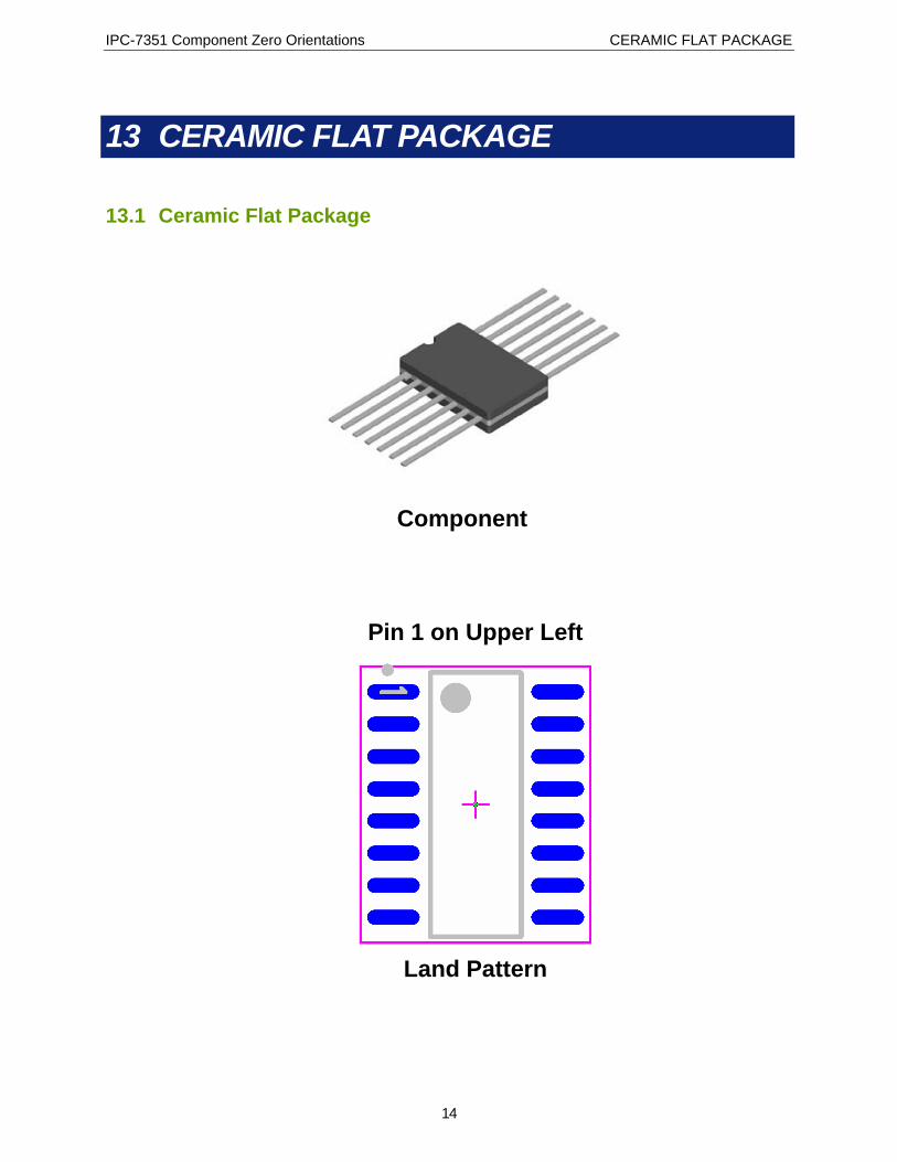
13 CERAMIC FLAT PACKAGE
13.1 Ceramic Flat Package
Component
Pin 1 on Upper Left
Land Pattern
IPC-7351 Component Zero Orientations CERAMIC QUAD FLAT PACKAGE
15
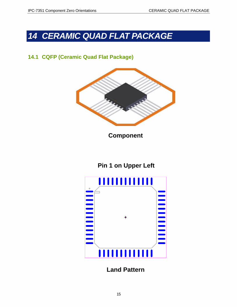
14 CERAMIC QUAD FLAT PACKAGE
14.1 CQFP (Ceramic Quad Flat Package)
Component
Pin 1 on Upper Left
Land Pattern
IPC-7351 Component Zero Orientations PLASTIC LEADED CHIP CARRIERS
16
15 PLASTIC LEADED CHIP CARRIERS
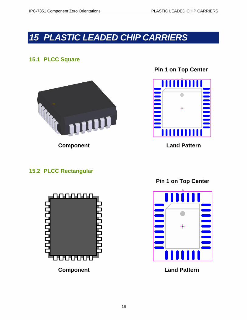
15.1 PLCC Square
Pin 1 on Top Center
Component Land Pattern
15.2 PLCC Rectangular
Pin 1 on Top Center
Component Land Pattern
IPC-7351 Component Zero Orientations LEADLESS CHIP CARRIERS
17
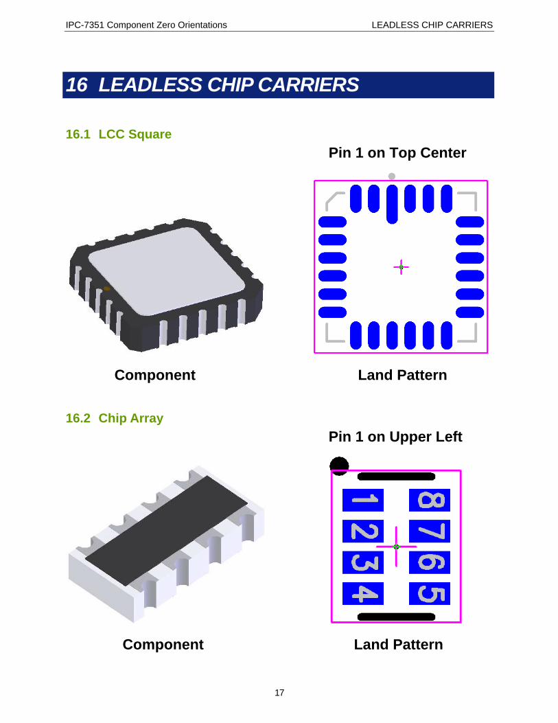
16 LEADLESS CHIP CARRIERS
16.1 LCC Square Pin 1 on Top Center
Component Land Pattern
16.2 Chip Array Pin 1 on Upper Left
Component Land Pattern
IPC-7351 Component Zero Orientations QUAD FLAT NO-LEAD
18
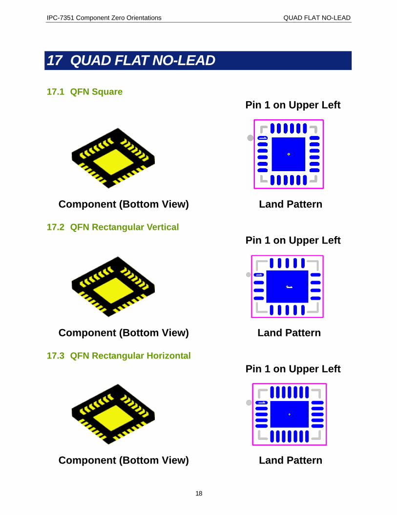
17 QUAD FLAT NO-LEAD
17.1 QFN Square Pin 1 on Upper Left
Component (Bottom View) Land Pattern
17.2 QFN Rectangular Vertical Pin 1 on Upper Left
Component (Bottom View) Land Pattern
17.3 QFN Rectangular Horizontal Pin 1 on Upper Left
Component (Bottom View) Land Pattern
Component Orientations BALL GRID ARRAY
19
18 BALL GRID ARRAY
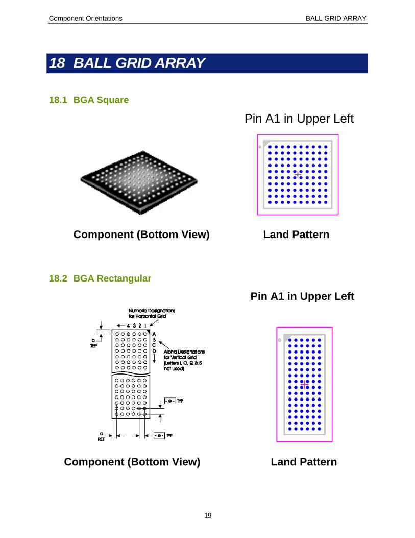
18.1 BGA Square
Pin A1 in Upper Left
Component (Bottom View) Land Pattern
18.2 BGA Rectangular
Pin A1 in Upper Left
Component (Bottom View) Land Pattern
Component Orientations COMPONENT ZERO ORIENTATIONS
20
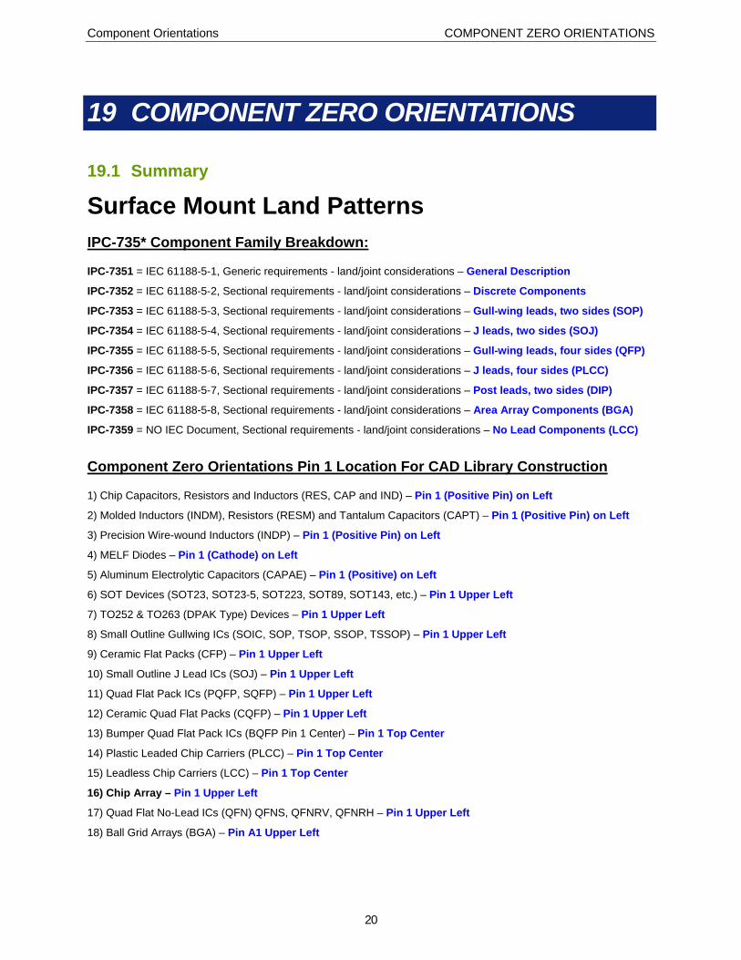
19 COMPONENT ZERO ORIENTATIONS
19.1 Summary
Surface Mount Land Patterns IPC-735* Component Family Breakdown:
IPC-7351 = IEC 61188-5-1, Generic requirements - land/joint considerations – General Description
IPC-7352 = IEC 61188-5-2, Sectional requirements - land/joint considerations – Discrete Components
IPC-7353 = IEC 61188-5-3, Sectional requirements - land/joint considerations – Gull-wing leads, two sides (SOP)
IPC-7354 = IEC 61188-5-4, Sectional requirements - land/joint considerations – J leads, two sides (SOJ)
IPC-7355 = IEC 61188-5-5, Sectional requirements - land/joint considerations – Gull-wing leads, four sides (QFP)
IPC-7356 = IEC 61188-5-6, Sectional requirements - land/joint considerations – J leads, four sides (PLCC)
IPC-7357 = IEC 61188-5-7, Sectional requirements - land/joint considerations – Post leads, two sides (DIP)
IPC-7358 = IEC 61188-5-8, Sectional requirements - land/joint considerations – Area Array Components (BGA)
IPC-7359 = NO IEC Document, Sectional requirements - land/joint considerations – No Lead Components (LCC)
Component Zero Orientations Pin 1 Location For CAD Library Construction
1) Chip Capacitors, Resistors and Inductors (RES, CAP and IND) – Pin 1 (Positive Pin) on Left
2) Molded Inductors (INDM), Resistors (RESM) and Tantalum Capacitors (CAPT) – Pin 1 (Positive Pin) on Left
3) Precision Wire-wound Inductors (INDP) – Pin 1 (Positive Pin) on Left
4) MELF Diodes – Pin 1 (Cathode) on Left
5) Aluminum Electrolytic Capacitors (CAPAE) – Pin 1 (Positive) on Left
6) SOT Devices (SOT23, SOT23-5, SOT223, SOT89, SOT143, etc.) – Pin 1 Upper Left
7) TO252 & TO263 (DPAK Type) Devices – Pin 1 Upper Left
8) Small Outline Gullwing ICs (SOIC, SOP, TSOP, SSOP, TSSOP) – Pin 1 Upper Left
9) Ceramic Flat Packs (CFP) – Pin 1 Upper Left
10) Small Outline J Lead ICs (SOJ) – Pin 1 Upper Left
11) Quad Flat Pack ICs (PQFP, SQFP) – Pin 1 Upper Left
12) Ceramic Quad Flat Packs (CQFP) – Pin 1 Upper Left
13) Bumper Quad Flat Pack ICs (BQFP Pin 1 Center) – Pin 1 Top Center
14) Plastic Leaded Chip Carriers (PLCC) – Pin 1 Top Center
15) Leadless Chip Carriers (LCC) – Pin 1 Top Center
16) Chip Array – Pin 1 Upper Left
17) Quad Flat No-Lead ICs (QFN) QFNS, QFNRV, QFNRH – Pin 1 Upper Left
18) Ball Grid Arrays (BGA) – Pin A1 Upper Left
Component Orientations APPENDIX A - EIA Survey for Component Orientation
21
20 APPENDIX A - EIA Survey for Component Orientation Date: 04 February 2003 TO: END USERS AND SUPPLIERS OF COMPONENT PACKAGES SUPPLIED ON TAPE FROM: ELECTRONIC INDUSTRIES ALLIANCE (EIA) AUTOMATED COMPONENT HANDLING COMMITTEE (ACH) SUBJECT: EIA SURVEY FOR ORIENTATION OF COMPONENTS SUPPLIED ON TAPE SPECIFICALLY: STANDARD EIA-481-B, “8 mm through 200 mm Embossed Carrier Taping and 8 mm & 12 mm Punched Carrier Taping of Surface Mount Components for Automatic Handling”. CAUTION: THE INDUSTRY STANDARD MAY CHANGE! WE REQUEST YOUR COMMENTS.
20.1 Purpose The Automated Component Handling Committee develops and maintains industry engineering standards and publications for tape, reels, magazines, trays, etc. for handling components in production. It also provides technical input to US national positions on related international standards issues and proposals. Based on a number of industry queries, the committee has decided to survey industry to determine the need for an improved standard for orientation of component packages in tape and reel. Pending the outcome of this survey, a change proposal to the EIA-481B standard will be prepared and presented for approval during 2003. This is your opportunity to have your comments considered. Please complete the survey attached to the e-mail as the file entitled, “Part 2” by 15 March 2003 and email the completed survey to the following address: [email protected]
20.2 Driving factors The following areas in EIA 481B can still cause confusion as to orientation: Factor 1 (F1): Ambiguity exists on how to interpret terminology such as ‘Termination #1’ and ‘SOT23-5’ Factor 2 (F2): Inconsistency exists on how components that share a common outline are oriented in tape; for example, a ‘SOT223’ and a ‘SOT89’ are supplied in tape with orientations that do not match. These factors result in ambiguity during the taping process for the supplier. These factors may also result in components that are supplied in orientations that are not acceptable for automating the component pick-and-place process for the end user. EIA-481B, Section 4.14 documents the current standard for determining component package orientation in tape.

Component Orientations APPENDIX A - EIA Survey for Component Orientation
22
20.3 Examples of Possible Conflict Driving factor F1 is illustrated by applying the current standard to a 5 termination ‘SOT23’ package (Figure 1a and 1b). The examples show that the same component package may have three different orientations in tape based on different package outline names as well as non standardized termination numbering conventions by various component manufacturers. Inconsistent orientation in tape for the same component creates an unacceptable condition for automating the component pick-and-place process.
Figure 1a: Internal Part number ‘X’, Approved Manufacturer ‘A’
Figure 1b: Internal Part number ‘X’, Approved Manufacturer ‘B’
Component Orientations APPENDIX A - EIA Survey for Component Orientation
23
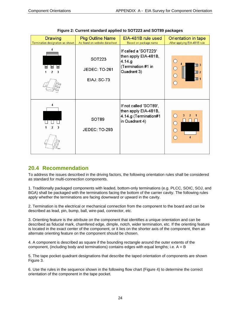
Driving factor F2 is illustrated by applying the current standard to a SOT223 and SOT89 package (Figure 2). The example shows that packages that share similar geometric attributes have two different orientations in tape. Pick-and-place equipment machine recognition systems identify component packages by the arrangement of terminations on the package body. Component packages with similar outlines should share the same orientation in tape to minimize possibility of confusion between the packages.
Component Orientations APPENDIX A - EIA Survey for Component Orientation
24
Figure 2: Current standard applied to SOT223 and SOT89 packages
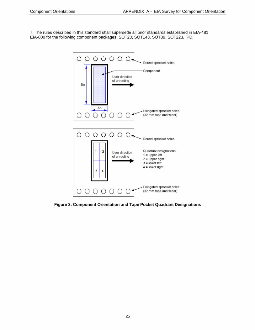
20.4 Recommendation To address the issues described in the driving factors, the following orientation rules shall be considered as standard for multi-connection components. 1. Traditionally packaged components with leaded, bottom-only terminations (e.g. PLCC, SOIC, SOJ, and BGA) shall be packaged with the terminations facing the bottom of the carrier cavity. The following rules apply whether the terminations are facing downward or upward in the cavity. 2. Termination is the electrical or mechanical connection from the component to the board and can be described as lead, pin, bump, ball, wire-pad, connector, etc. 3. Orienting feature is the attribute on the component that identifies a unique orientation and can be described as fiducial mark, chamfered edge, dimple, notch, wider termination, etc. If the orienting feature is located in the exact center of the component, or it lies on the shorter axis of the component, then an alternate orienting feature on the component should be chosen. 4. A component is described as square if the bounding rectangle around the outer extents of the component, (including body and terminations) contains edges with equal lengths; i.e. A = B 5. The tape pocket quadrant designations that describe the taped orientation of components are shown Figure 3. 6. Use the rules in the sequence shown in the following flow chart (Figure 4) to determine the correct orientation of the component in the tape pocket.
Component Orientations APPENDIX A - EIA Survey for Component Orientation
25
7. The rules described in this standard shall supersede all prior standards established in EIA-481 EIA-800 for the following component packages: SOT23, SOT143, SOT89, SOT223, IPD.
Figure 3: Component Orientation and Tape Pocket Quadrant Designations
Component Orientations APPENDIX A - EIA Survey for Component Orientation
26
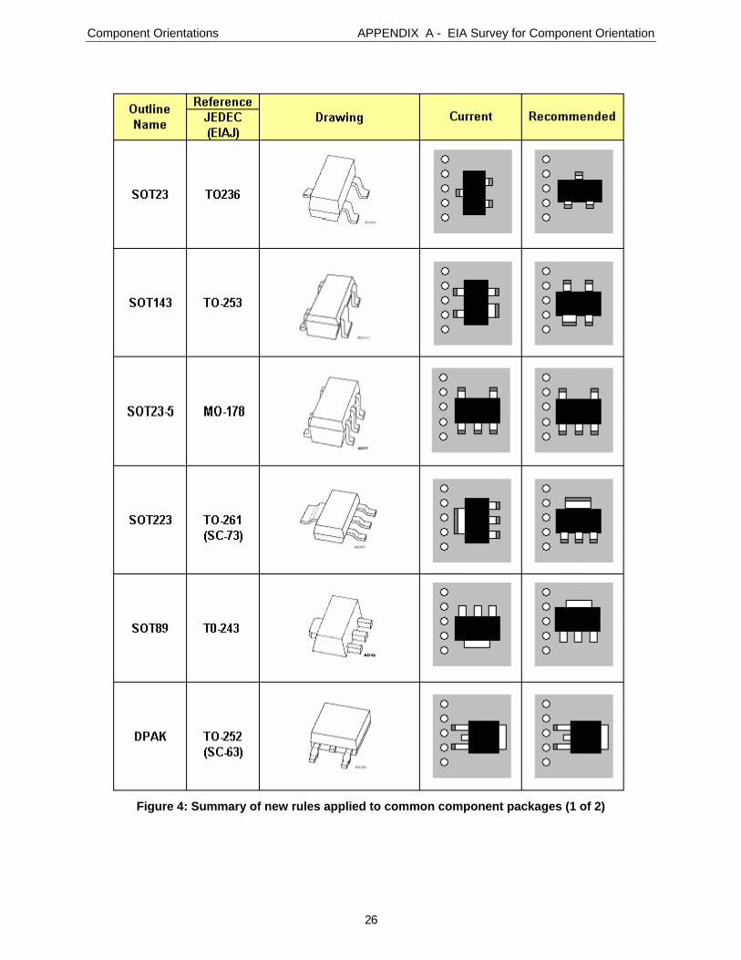
Figure 4: Summary of new rules applied to common component packages (1 of 2)
Component Orientations APPENDIX A - EIA Survey for Component Orientation
27
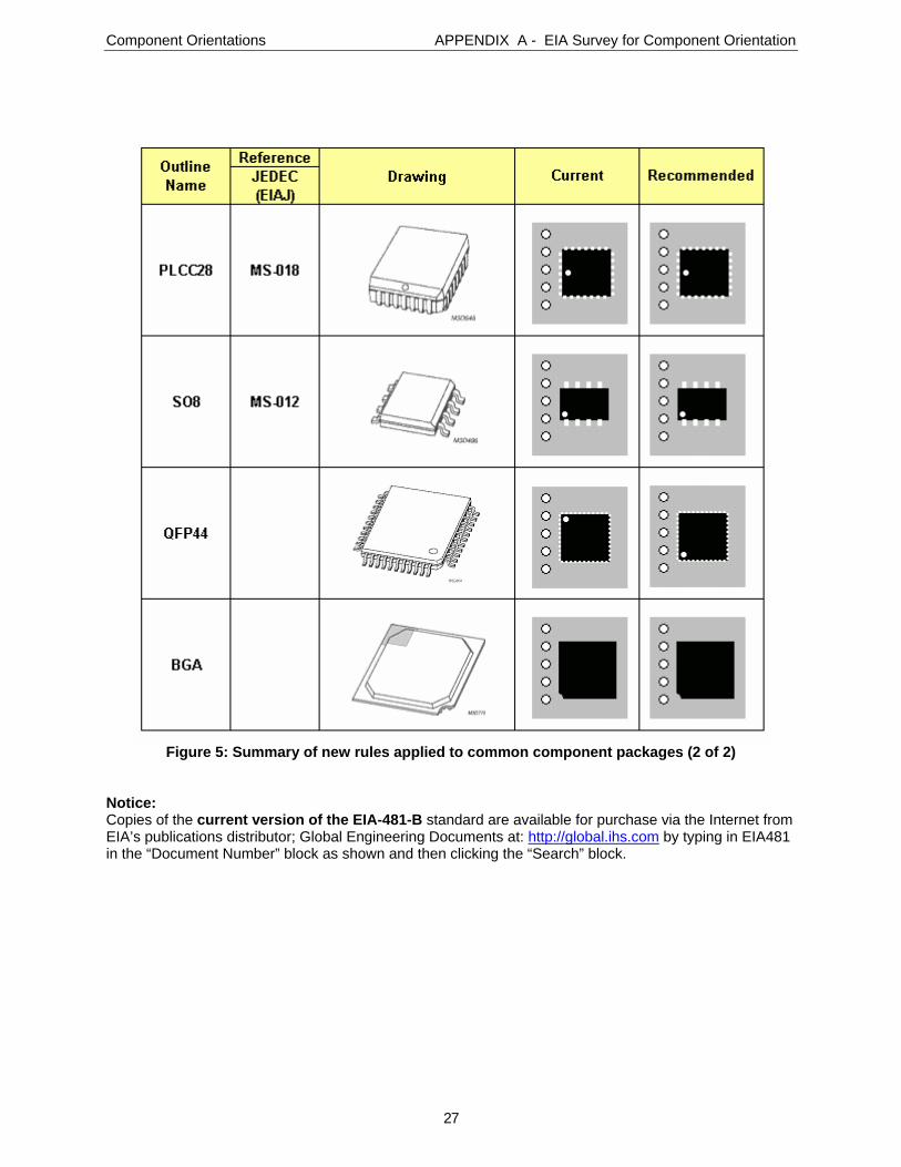
Figure 5: Summary of new rules applied to common component packages (2 of 2)
Notice: Copies of the current version of the EIA-481-B standard are available for purchase via the Internet from EIA’s publications distributor; Global Engineering Documents at: http://global.ihs.com by typing in EIA481 in the “Document Number” block as shown and then clicking the “Search” block.
Component Orientations APPENDIX A - EIA Survey for Component Orientation
28
20.5 Presentation of Results Edward F. Mikoski, Jr. Spring 2003 (Excerpts) Component Manufacturer (on orientation issues)
• Our customer base has conflicting perceptions as to how the orientation standard is understood. • Based upon its wording today, we have little leverage to request orientation consistency. • Wholesale changes will be difficult and cost prohibitive. However, all new packages and tooling
releases should follow the proposed changes. End User (on the proposed new rules)
• This would require us to overhaul our test handlers to accommodate a 90 degree rotation of the device.
• The cost involved in a project such as this would be more than we plan to budget for the test equipment.
• To upgrade, the equipment will need a new or modified feeder system, orientation station and Pick and Place head design.
• Modifications will need to be made to the vision inspection systems allowing inspection of the part at the proposed orientation.
EMS
• Under new rules the machine operator will have to reprogram orientation of existing products. End User (on other issues that the committee should address)
• 1. Adopting the Cartesian coordinate system for identifying quadrants. • 2. Addressing of bare die orientation in tape. • 3. Addressing of component orientation in matrix trays as illustrated by example methodology
used in the EIA Orientation Survey. General Comment Received
• The proposal deviates for many packages from what is currently used. We feel that inconsistencies remain even with the new standard since the "old" orientations will remain on the market. Hence, we will have more inconsistencies in the future. To overcome that we propose that there should be at least a joint JEITA - EIA standard.
Component Orientations APPENDIX B – Internet Search Results
29
21 APPENDIX B – Internet Search Results
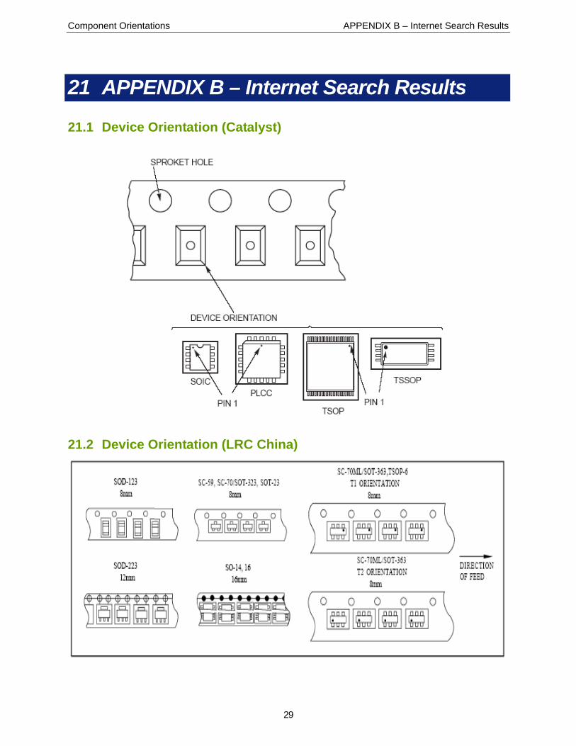
21.1 Device Orientation (Catalyst)
21.2 Device Orientation (LRC China)
Component Orientations APPENDIX B – Internet Search Results
30
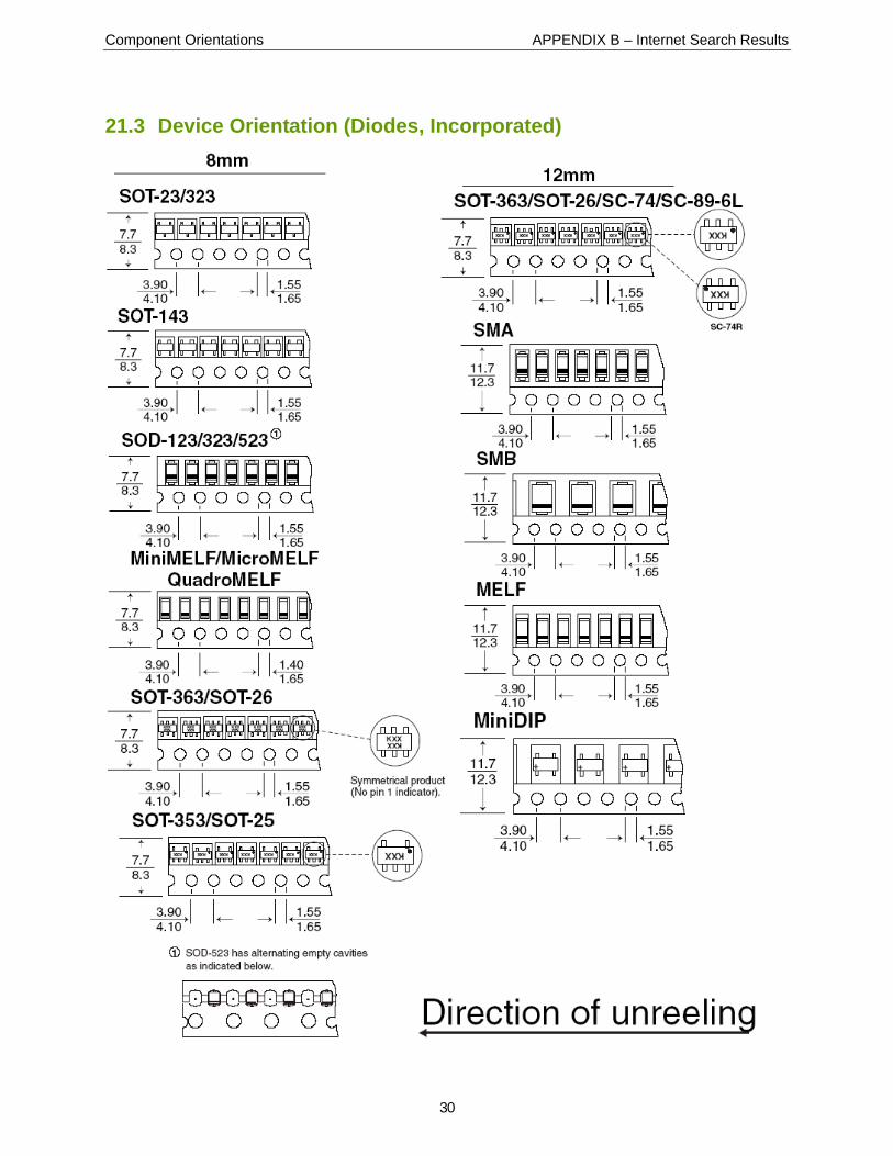
21.3 Device Orientation (Diodes, Incorporated)
Component Orientations APPENDIX B – Internet Search Results
31
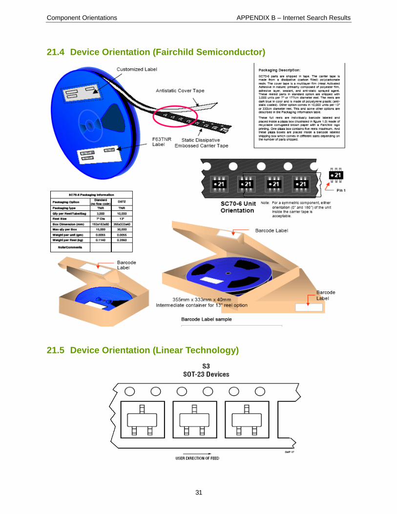
21.4 Device Orientation (Fairchild Semiconductor)
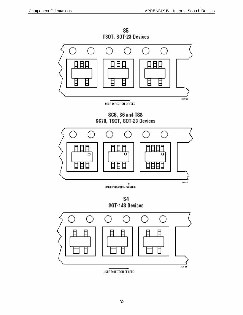
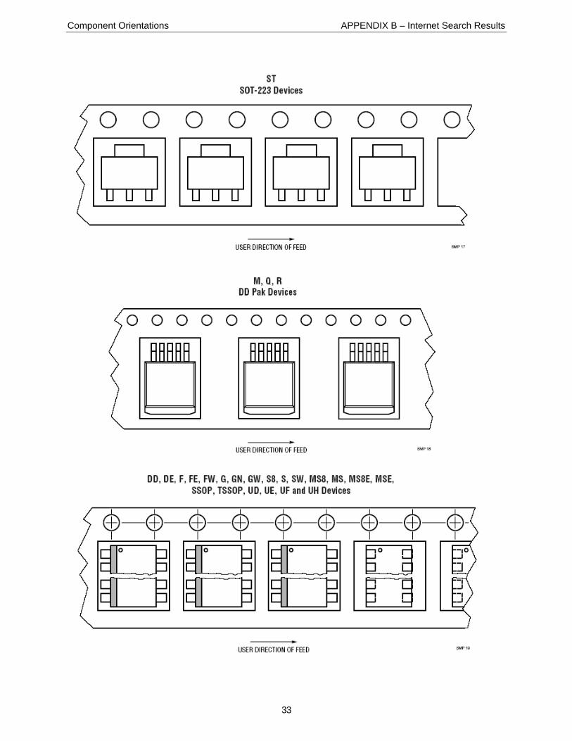
21.5 Device Orientation (Linear Technology)
Component Orientations APPENDIX B – Internet Search Results
32
Component Orientations APPENDIX B – Internet Search Results
33
Component Orientations APPENDIX B – Internet Search Results
34
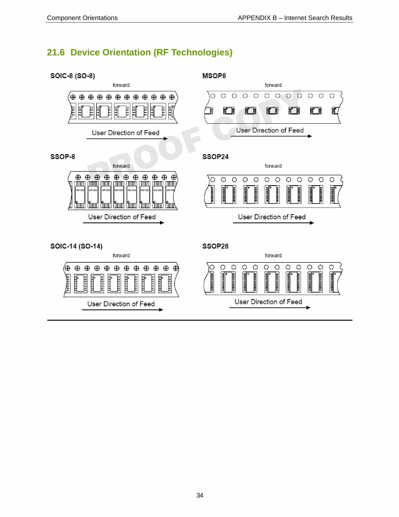
21.6 Device Orientation (RF Technologies)

Component Orientations APPENDIX B – Internet Search Results
35
Component Orientations APPENDIX B – Internet Search Results
36
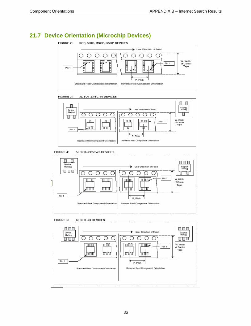
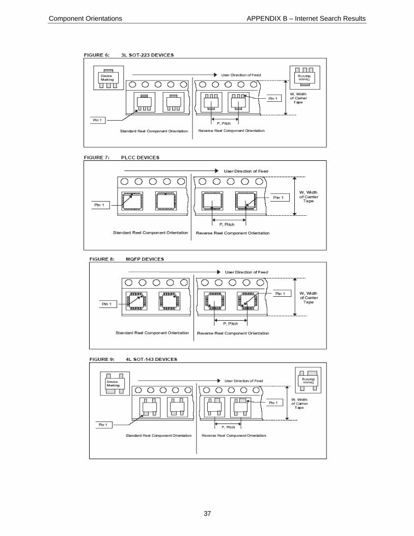
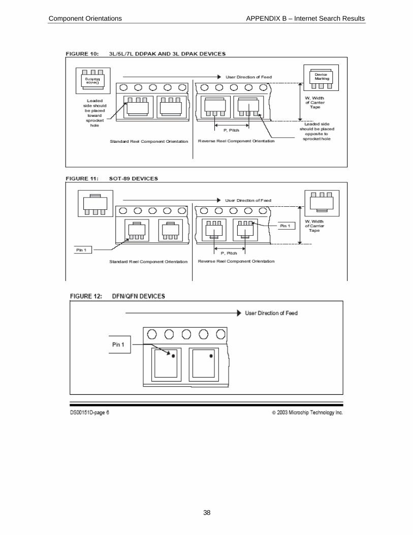
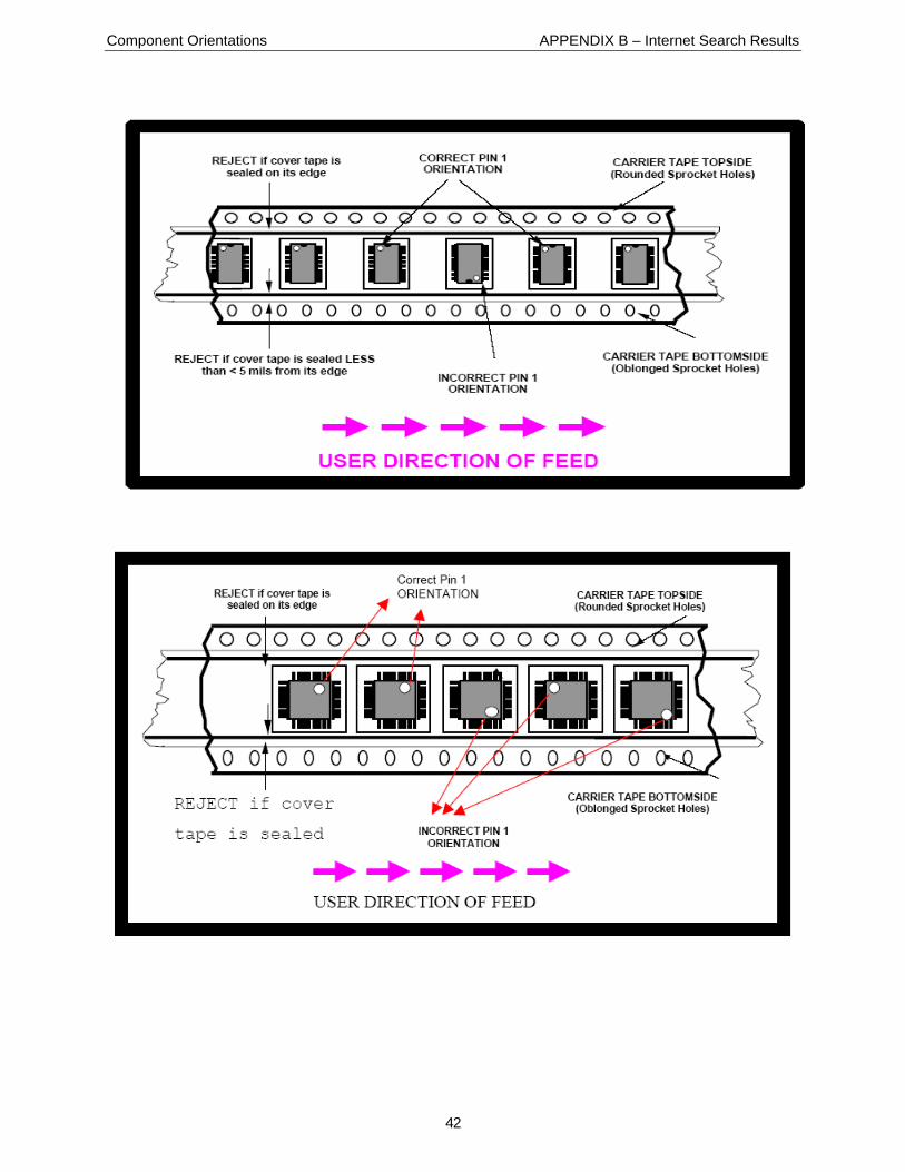
21.7 Device Orientation (Microchip Devices)
Component Orientations APPENDIX B – Internet Search Results
37
Component Orientations APPENDIX B – Internet Search Results
38
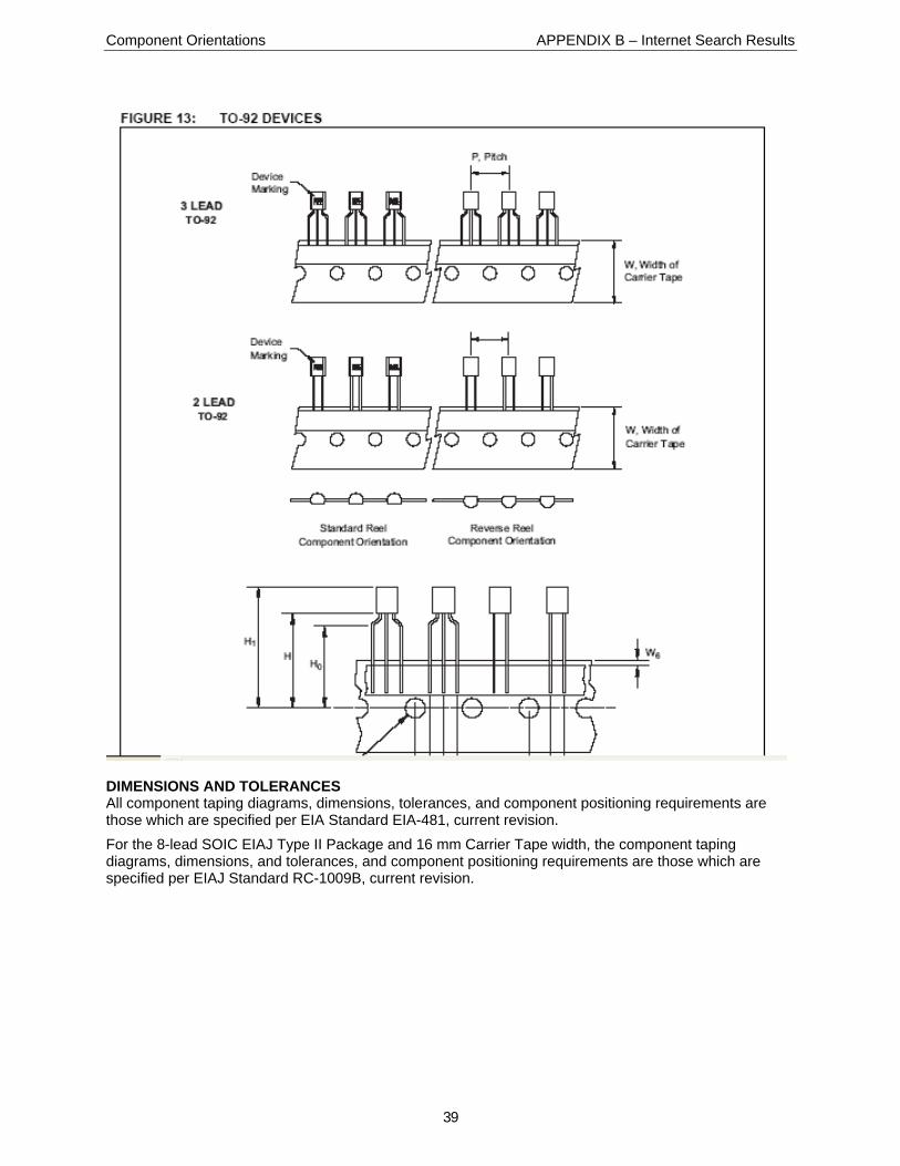
Component Orientations APPENDIX B – Internet Search Results
39
DIMENSIONS AND TOLERANCES All component taping diagrams, dimensions, tolerances, and component positioning requirements are those which are specified per EIA Standard EIA-481, current revision. For the 8-lead SOIC EIAJ Type II Package and 16 mm Carrier Tape width, the component taping diagrams, dimensions, and tolerances, and component positioning requirements are those which are specified per EIAJ Standard RC-1009B, current revision.
Component Orientations APPENDIX B – Internet Search Results
40
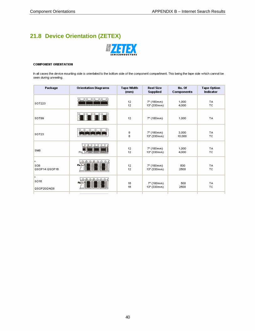
21.8 Device Orientation (ZETEX)
Component Orientations APPENDIX B – Internet Search Results
41
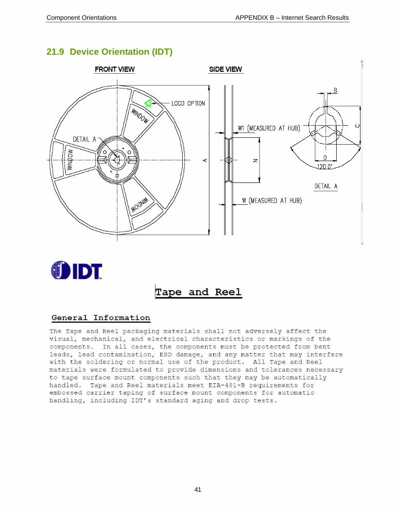
21.9 Device Orientation (IDT)
Component Orientations APPENDIX B – Internet Search Results
42

Component Orientations APPENDIX C – Comment Form
43
22 APPENDIX C – Comment Form The purpose of this form is to provide the Technical Committees of IPC and the IEC with input from the industry regarding usage of the subject of Zero Component Orientation Recommendations. Individuals or companies are invited to submit comments to IPC. All comments will be collected and dispersed to the appropriate committee(s). If you can provide input, please complete this form and return to:
IPC-Association Connecting Electronics Industries 3000 Lakside Drive Suite 309S Bannockburn, IL, 60015 Tel: 847-615-7100 Fax: 847-615-7105
Web: www.ipc.org Email: [email protected]
1. I recommend changes to the following:
Requirement ________________________________________________________ Paragraph number ___________________________________________________ Other______________________________________________________________ 2. Recommendations for correction: _________________________________________ ____________________________________________________________________________________________________________________________________________________________________________________________________________________________________________________________ 3. Other suggestions for document improvement: ________________________________________________________________________________________________________________________________________________________________________ Submitted by: Name ________________________________________Telephone________________ Company _____________________________________ E-mail ________________ Address _______________________________________________________________ City/State/Zipcode ________________________________________________________ Date: ______________________
Component Orientations CREDITS
44
23 CREDITS
23.1 Contributions Component pictures provided by Topline Components ©1997, TopArt Clip Art Companies that provided written and graphic materials contained within this document:
Diodes Incorporated Diodes Incorporated 3050 E. Hillcrest Drive Westlake Village, CA 91362-3154 Tel: 805-446-4800 Fax: 805-446-4850 Web: http://www.diodes.com
Electronic Industries Alliance Edward F. Mikoski, Jr. 2500 Wilson Blvd. Arlington, VA 22201 Tel: 703-907-7500 Web: http://www.eia.org
IDT 2975 Stender Way Santa Clara, CA 95054 Tel: 408-727-6116 Fax: 408-492-8674 Web: http://www.idt.com
IPC – Association Connecting Electronics Industries Dieter Bergman
3000 Lakside Drive Suite 309S Bannockburn, IL, 60015 Tel: 847-615-7100 Fax: 847-615-7105
Email: [email protected] Web: http://www.ipc.org
PCB Libraries, Inc. Tom Hausherr 701 Lee Street Des Plaines, IL 60016 Tel: 877-722-4441 Fax: 847.745.0450 Email: [email protected] Web: http://www.PCBLibraries.com
Zetex Semiconductors Web: http://www.zetex.com
Fairchild Semiconductor Corporation 82 Running Hill Road South Portland, ME 04106 Phone: 207-775-8100 web: www.fairchildsemi.com
Linear TechnologyCorporation 1630 McCarthy Blvd Milpitas, CA 95035 USA Phone: 408-432-1900 Fax: +1-408-434-0507 web: www.linear-tech.com
Component Orientations CREDITS
45
Microchip Technology Incorporated 2355 W. Chandler Blvd. Chandler, AZ 85224 Phone: 480-792-7200 Fax: 480-899-9210 web: www.microchip.com
M/A-Com Incorporated 1011 Pawtucket Boulevard Lowell, MA 01853 Phone: 978-442-5000 web: www.macom.com
Catalyst Semiconductor Corporate Headquarters 1250 Borregas Avenue Sunnyvale, CA 94089 Phone: 408-542-1000 Fax: 408-542-1200 web: www.catalyst-semiconductor.com