Embed Size (px)
Citation preview
Complete VLSI Implementation of Improved Low
Complexity Chase Reed-Solomon Decoders
by
Wei An
B.S., Shanghai Jiao Tong University (1993)M.S., University of Delaware (2000)
MASSACHUSETTS INSTITUTEOF TECHNOLOGY
OCT 3 5 2010
LIBRARIES
Submitted to the Department of Electrical Engineering and ComputerScience
in partial fulfillment of the requirements for the degree of
Electrical Engineer
at the
MASSACHUSETTS INSTITUTE OF TECHNOLOGY
ARCHVES
September 2010
@ Massachusetts Institute of Technology 2010. All rights reserved.
Author .Department
Certified by.......
of Electrical Engmeering and Computer Science' September 3, 2010
// U / Vladimir M. StojanovidAssociate Professor
Thesis Supervisor~1 ~
Accepted by...................Terry P. Orlando
Chairman, Department Committee on Graduate Theses

2
Complete VLSI Implementation of Improved Low
Complexity Chase Reed-Solomon Decoders
by
Wei An
Submitted to the Department of Electrical Engineering and Computer Scienceon September 3, 2010, in partial fulfillment of the
requirements for the degree ofElectrical Engineer
Abstract
This thesis presents a complete VLSI design of improved low complexity chase (LCC)decoders for Reed-Solomon (RS) codes. This is the first attempt in published researchthat implements LCC decoders at the circuit level.
Based on the joint algorithm research with University of Hawaii, we propose sev-eral new techniques for complexity reduction in LCC decoders and apply them in theVLSI design for RS [255, 239,17] (LCC255) and RS [31, 25, 7] (LCC31) codes. Themajor algorithm improvement is that the interpolation is performed over a subset oftest vectors to avoid redundant decoding. Also the factorization formula is reshapedto avoid large computation complexity overlooked in previous research. To maintainthe effectiveness of algorithm improvements, we find it necessary to adopt the system-atic message encoding, instead of the evaluation-map encoding used in the previouswork on interpolation decoders.
The LCC255 and LCC31 decoders are both implemented in 90nm CMOS processwith the areas of 1.01mm 2 and 0.255mm 2 respectively. Simulations show that with1.2V supply voltage they can achieve the energy efficiencies of 67pJ/bit and 34pJ/bitat the maximum throughputs of 2.5Gbps and 1.3Gbps respectively. The proposedalgorithm changes, combined with optimized macro- and micro-architectures, resultin a 70% complexity reduction (measured with gate count). This new LCC design alsoachieves 17x better energy-efficiency than a standard Chase decoder (projected fromthe most recent reported Reed Solomon decoder implementation) for equivalent area,latency and throughput. The comparison of the two decoders links the significantlyhigher decoding energy cost to the better decoding performance. We quantitativelycompute the cost of the decoding gain as the adjusted area of LCC255 being 7.5 timesmore than LCC31.
Thesis Supervisor: Vladimir M. StojanovidTitle: Associate Professor

4

Acknowledgments
I want to thank Dr. Fabian Lim and Professor Aleksandar Kavoid from University of
Hawaii at Manoa for the cooperation on the algorithm investigation. I also want to
thank Professor Vladimir Stojanovid for his inspiring supervision. Finally, I want to
acknowledge Analog Devices, Inc. for supporting my study at MIT.

6
Contents
1 Introduction
1.1 Reed-Solomon codes for forward error correction . . . . . . . . . . . .
1.2 Low complexity Chase decoders for RS codes . . . . . . . . . . . . . .
1.3 Major contributions and thesis topics . . . . . . . . . . . . . . . . . .
2 Background
2.1 Encoders and HDD decoders for Reed-Solomon codes . . . . . . . . .
2.2 Channel model, signal-to-noise ratio and reliability . . . . . . . . . .
2.3 The LCC decoding algorithm . . . . . . . . . . . . . . . . . . . . . .
3 Algorithm Refinements and Improvements
3.1 Test vector selection . . . . . . . . . . . . . . . . . . . . . . . . . . .
3.2 Reshaping of the factorization formula . . . . . . . . . . . . . . . . .
3.3 Systematic message encoding . . . . . . . . . . . . . . . . . . . . . .
4 VLSI Design of LCC Decoders
4.1 Digital signal resolution and C++
4.2 Basic Galois field operations
4.3 System level considerations . . . .
4.4 Pre-interpolation processing . . .
4.4.1 Stage I . . . . . . . . . . .
4.4.2 Stage II . . . . . . . . . .
4.4.3 Stage III . . . . . . . . . .
simulation
13
13
15
16
19
19
22
23
29
29
32
32
35
. . . . . . . . . . . . 35
. . . . . . . . . . . . 37
. . . . . . . . . . . . 39
. . . . . . . . . . . . 40
. . . . . . . . . . . . 41
. . . . . . . . . . . . 43
. . . . . . . . . . . . 44
4.5 Interpolation . . . . . . . . . . . . . . . . . . . . . . .
4.5.1 The interpolation unit . . . . . . . . . . . . . .
4.5.2 The allocation of interpolation units . . . . . .
4.5.3 Design techniques for interpolation stages . . .
4.6 The RCF algorithm and error locations . . . . . . . . .
4.7 Factorization and codeword recovery . . . . . . . . . .
4.8 Configuration module . . . . . . . . . . . . . . . . . . .
5 Design Results and Analysis
5.1 Complexity distribution of LCC design . . . . . . . .
5.2 Comparison to standard Chase decoder based on HDD
5.3 Comparison to previous LCC work . . . . . . . . . .
5.4 Comparison of LCC255 to LCC31 . . . . . . . . . . .
6 Conclusion and Future Work
6.1 C onclusion . . . . . . . . . . . . . . . . . . . . . . . . . . . . . . . . .
6.2 Future work . . . . . . . . . . . . . . . . . . . . . . . . . . . . . . . .
A Design Properties and Their Relationship
B Supply Voltage Scaling and Process Technology Transformation
C I/O interface and the chip design issues
D Physical Design and Verification
D.1 Register file and SRAM generation . . . . . . . . . . . . . . . . . .
D.2 Synthesis, place and route . . . . . . . . . . . . . . . . . . . . . . .
D.3 LVS and DRC design verification . . . . . . . . . . . . . . . . . . .
D.4 Parasitic extraction and simulation . . . . . . . . . . . . . . . . . .
. . . . . . . . 44
. . . . . . . . 44
. . . . . . . . 46
. . . . . . . . 50
. . . . . . . . 52
. . . . . . . . 55
. . . . . . . . 57
59
. . . . . . . . 60
. . . . . . . 64
. . . . . . . . 66
. . . . . . . . 67
73
73
74
75
77
81
85
85
85
90
93

List of Figures
3-1 Simple rj = 3 example to illustrate the difference between the standard
Chase and Tokushige et. al. [30] test vector sets. The standard Chase
test vector set has size 27 = 8. The Tokushige test vector set covers a
similar region as the Chase, however with only h = 4 test vectors. . . 30
3-2 Performance of test vector selection method for RS[255, 239,17]. . . . 31
4-1 Comparison of fixed-point data types for RS[255, 239, 17] LCC decoder. 36
4-2 Galois field adder . . . . . . . . . . . . . . . . . . . . . . . . . . . . . 37
4-3 The XTime function . . . . . . . . . . . . . . . . . . . . . . . . . . . 38
4-4 Galois field multiplier . . . . . . . . . . . . . . . . . . . . . . . . . . . 38
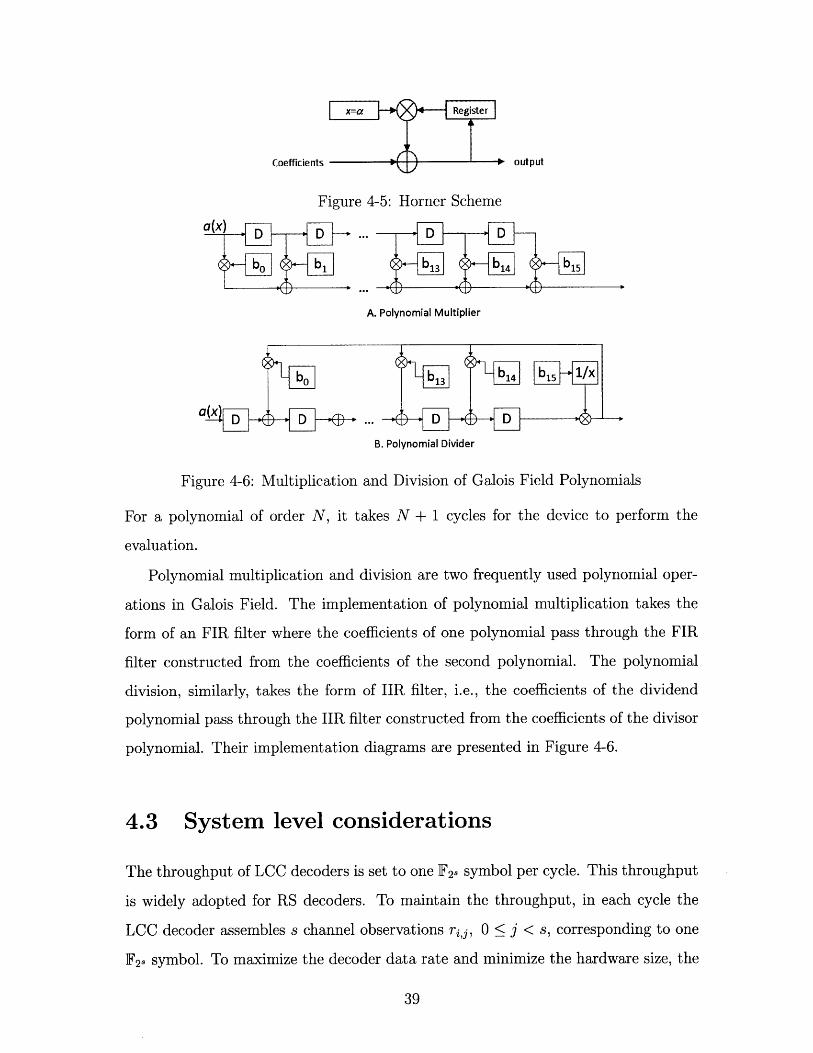
4-5 Horner Scheme . . . . . . . . . . . . . . . . . . . . . . . . . . . . . . 39
4-6 Multiplication and Division of Galois Field Polynomials . . . . . . . . 39
4-7 VLSI implementation diagram. . . . . . . . . . . . . . . . . . . . . . 40
4-8 Data and reliability construction . . . . . . . . . . . . . . . . . . . . . 41
4-9 Sort by the reliability metric . . . . . . . . . . . . . . . . . . . . . . . 42
4-10 Compute the error locator polynomial . . . . . . . . . . . . . . . . . . 43
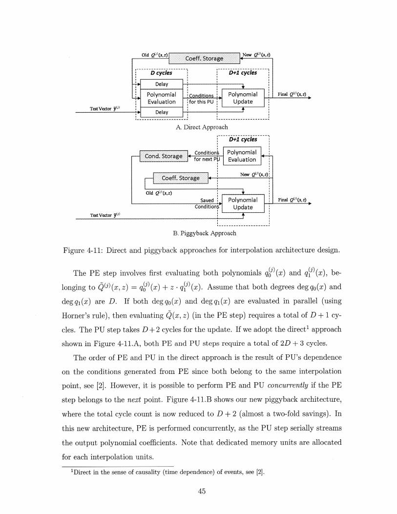
4-11 Direct and piggyback approaches for interpolation architecture design. 45
4-12 The Interpolation Unit. . . . . . . . . . . . . . . . . . . . . . . . . . . 47
4-13 Tree representation of the (full) test vector set (2.12) for LCC255 de-
coders, when 71 = 8 (i.e. size 28). The tree root starts from the first
point outside J (recall the complementary set J has size N - K = 16). 47
4-14 Sub-tree representation of the h = 16 fixed paths, chosen using the
Tokushige et. al. procedure [30] (also see Chapter 3) for LCC255 decoder. 48
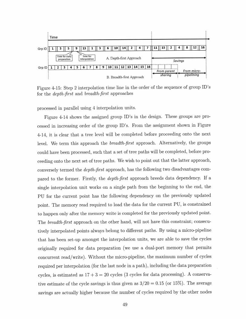
4-15 Step 2 interpolation time line in the order of the sequence of group
ID's for the depth-first and breadth-first approaches . . . . . . . . . . 49
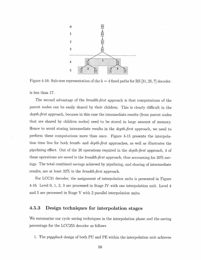
4-16 Sub-tree representation of the h = 4 fixed paths for RS [31, 25, 7 decoder. 50
4-17 RCF block micro-architecture. . . . . . . . . . . . . . . . . . . . . . . 53
4-18 Implementation diagram of the RCF algorithm. . . . . . . . . . . . . 54
4-19 Diagram for root collection. . . . . . . . . . . . . . . . . . . . . . . . 55
4-20 Detailed implementation diagram of Stage VII. . . . . . . . . . . . . 56
5-1 The circuit layout of the LCC design . . . . . . . . . . . . . . . . . . 60
5-2 Complexity distribution v.s. number of test vectors h . . . . . . . . . 64
5-3 Decoding energy cost v.s. maximum throughput with supply voltage
ranging from 0.6V to 1.8V . . . . . . . . . . . . . . . . . . . . . . . . 69
5-4 Decoding energy cost v.s. adjusted area with constant throughput and
latency as the supply voltage scales from 0.6V to 1.8V . . . . . . . . 70
5-5 Decoding energy cost v.s. adjusted area with equivalent/constant
throughput and latency as the supply voltage scales from 0.6V to 1.8V 71
C-1 The chip design diagram . . . . . . . . . . . . . . . . . . . . . . . . . 83
D-1 ASIC Design Flow. . . . . . . . . . . . . . . . . . . . . . . . . . . . . 86
D-2 Floorplan of the LCC255 decoder . . . . . . . . . . . . . . . . . . . . 89
D-3 Floorplan of the LCC31 decoder . . . . . . . . . . . . . . . . . . . . . 90
D-4 Floorplan of the I/O interface . . . . . . . . . . . . . . . . . . . . . . 91
D-5 The circuit layout of the complete chip design . . . . . . . . . . . . . 92

List of Tables
5.1 Implementation results for the proposed LCC VLSI design . . . . . . 60
5.2 Gate count of the synthesized LCC decoder . . . . . . . . . . . . . . 62
5.3 Complexity Distribution of the synthesized LCC decoder . . . . . . . 63
5.4 Comparison of the proposed LCC with HDD RS decoder and the cor-
responding standard Chase decoder . . . . . . . . . . . . . . . . . . . 66
5.5 Area adjustment for comparison of decoding energy-costs . . . . . . . 67
5.6 Multiplier usage in the proposed LCC decoder . . . . . . . . . . . . . 68
5.7 RAM usage in the proposed LCC decoder . . . . . . . . . . . . . . . 68
5.8 Comparison of the proposed LCC architecture and the work in [33] . 68
5.9 Computed limits of clock frequency and adjusted area along with through-
put and latency for LCC31 and LCC255 . . . . . . . . . . . . . . . . 71
C.1 Number of Bits of Decoder Interface . . . . . . . . . . . . . . . . . . 81
C.2 The I/O interface to the outside environment . . . . . . . . . . . . . 83
D.1 Memory usage in the chip design . . . . . . . . . . . . . . . . . . . . 87
D.2 Physical parameters of the circuit layout . . . . . . . . . . . . . . . . 93
D.3 Testing cases in transient simulations . . . . . . . . . . . . . . . . . . 93

12

Chapter 1
Introduction
In this thesis, we improve and implement the low complexity chase (LCC) decoders for
Reed-Solomon (RS) codes. The complete VLSI design is the first effort in published
research for LCC decoders. In this chapter, we briefly review the history of Reed-
Solomon codes and LCC algorithms. Then we outline the contributions and the
organization of the thesis.
1.1 Reed-Solomon codes for forward error correc-
tion
In data transmission, noisy channels often introduce errors in received information
bits. Forward Error Correction (FEC) is a method that is often used to enhance the
reliability of data transmission. In general, an encoder on the transmission side trans-
forms message vectors into codewords by introducing a certain amount of redundancy
and enlarging the distance'between codewords. On the receiver side, a contaminated
codeword, namely the senseword, is processed by a decoder that attempts to detect
and correct errors in its procedure of recovering the message bits.
Reed-Solomon (RS) codes are a type of algebraic FEC codes that were introduced
by Irving S. Reed and Gustave Solomon in 1960 [27]. They have found widespread
'There are various types of distance defined between codeword vectors. See [23] for details.
applications in data storage and communications due to their simple decoding and
their capability to correct bursts of errors [23]. The decoding algorithm for RS codes
was first derived by Peterson [26]. Later Berlekamp [3] and Massey [25] simplified the
algorithm by showing that the decoding problem is equivalent to finding the shortest
linear feedback shift register that generates a given sequence. The algorithm is named
after them as the Berlekamp-Massey algorithm (BMA) [23]. Since the invention
of the BMA, much work has been done on the development of RS hard-decision
decoding (HDD) algorithms. The most notable work is the application of the Euclid
Algorithm [29] for the determination of the error-locator polynomial. Berlekamp and
Welch [4] developed an algorithm (the Berlekamp-Welch(B-W) algorithm) that avoids
the syndrome computation, the first step required in all previously proposed decoding
algorithms. All these algorithms, in spite of their various features, can correct the
number of errors up to half the minimum distance dmin of codewords. There had been
no improvement on decoding performance for over 45 years since the introduction of
RS codes.
In 1997, a breakthrough by Sudan made it possible to correct more errors than
previous algebraic decoders [28]. A bivariate polynomial Q(X, Y) is interpolated over
the senseword. The result is shown to contain, in its y-linear factors, all codewords
within a decoding radius t > dmin/2. The complexity of the algorithm, however,
increases exponentially with the achievable decoding radius t. Sudan's work renewed
research interest in this area, yielding new RS decoders such as the Guruswarmi-Sudan
algorithm [9], the bit-level generalized minimum distance (GMD) decoder [12], and
the Koetter-Vardy algorithm [16].
The Koetter-Vardy algorithm generalizes Sudan's work by assigning multiplicities
to interpolation points. The assignment is based on the received symbol reliabili-
ties [16]. It relaxes Sudan's constraint of passing Q(x, y) through all received values
with equal multiplicity and results in a decoding performance significantly surpass-
ing the Guruswarmi-Sudan algorithm with comparable decoding complexity. Still,
the complexity of the Koetter-Vardy algorithm quickly increases as the multiplicities
increase. Extensive work has been done to reduce core component complexity of the

Sudan algorithm based decoders, namely interpolation and factorization [7, 15, 24].
Many decoder architectures have been proposed, e.g. [1, 13]. However, the Koetter-
Vardy algorithm still remains un-implementable from a practical standpoint.
1.2 Low complexity Chase decoders for RS codes
In 1972, Chase [6] developed a decoding architecture, non-specific to the type of
code, which increases the performance of any existing HDD algorithms. Unlike the
Sudan-like algorithms, which enhance the decoding performance via a fundamentally
different approach from the HDD procedure, the Chase decoder achieves the en-
hancement by applying multiple HDD decoders to a set of test vectors. In traditional
HDD, a senseword is obtained via the maximum a-posteriori probability (MAP) hard-
decision over the observed channel outputs. In Chase decoders, however, a test-set
of hard-decision vectors are constructed based on the reliability information. Each
of such test vectors is individually decoded by an HDD decoder. Among successfully
decoded test vectors, the decoding result of the test vector of highest a-posteriori
probability is selected as the final decoding result. Clearly, the performance increase
achieved by the Chase decoder comes at the expense of multiple HDD decoders with
the complexity proportional to the number of involved test vectors. To construct the
test-set, q least reliable locations are determined and vectors with all possible symbols
in these locations are considered. Consequently, the number of test vectors and the
complexity of Chase-decoding increase exponentially with q.
Bellorado and Kavoid [2] showed that the Sudan algorithm can be used to im-
plement Chase decoding for RS codes, however, with decreased complexity. Hence
the strategy is termed the low complexity Chase (LCC), as opposed to the standard
Chase. In the LCC, all interpolations are limited to a multiplicity of one. Application
of the coordinate transformation technique [8, 17] significantly reduces the number of
interpolation points. In addition, the reduced complexity factorization (RCF) tech-
nique proposed by Bellorado and Kavoid, further reduces the decoder complexity, by
selecting only a single interpolated polynomial for factorization [2]. The LCC has
been shown to achieve performance comparable to Koetter-Vardy algorithm, however
at lower complexity.
Recently, a number of architectures have been proposed for the critical LCC
blocks, such as backward interpolation [15] and factorization elimination [14], [33].
However, a full VLSI micro-architecture and circuit level implementation of the LCC
algorithm still remains to be investigated. This is the initial motivation of the research
presented in the thesis.
1.3 Major contributions and thesis topics
This thesis presents the first2 , complete VLSI implementation of LCC decoders. The
project follows the design philosophy that unifies multiple design levels such as al-
gorithm, system architecture and device components. Through the implementation-
driven system design, algorithms are first modified to significantly improve the hard-
ware efficiency. As the result of the joint research of MIT and University of Hawaii,
the main algorithm improvements include test vector selection, reshaping of the fac-
torization formula and the adoption of systematic encoding.
Two decoders, LCC255 and LCC31 (for RS [255, 239,17] and RS [31, 25, 7] codes
respectively), are designed with Verilog HDL language. Significant amount of effort is
devoted to the optimization of the macro- and micro architectures and various cycle
saving techniques are proposed for the optimization of each pipeline stages. While
being optimized, each component is designed with the maximal flexibility so they
can be easily adapted to meet new specifications. The component flexibility greatly
supports the design of two LCC decoders simultaneously.
The Verilog design is synthesized, placed-and-routed and verified in a represen-
tative 90nm CMOS technology. The physical implementation goes throughput com-
prehensive verifications and is ready for tape-out. We obtain the power and timing
estimation of each decoder by performing simulations on the netlist with parasitics
2In previously published literature (e.g. [15] and [14]), the described LCC architecture designswere incomplete, and were focused only on selected decoder components.

extracted from the circuit layout. The measurements from the implementation and
simulations provide data for comprehensive analysis on several aspects of the design,
such as system complexity distribution and reduction, decoding energy-cost of LCC
compared to Standard Chase and comparison between LCC255 and LCC31 decoders.
The thesis topics are arranged as follows.
Chapter 2 exposes the background of LCC and the previous techniques for com-
plexity reduction.
Chapter 3 presents new algorithm and architecture proposals that are essential
for further complexity reduction and efficient hardware implementation.
Chapter 4 presents in detail the VLSI hardware design of LCC255 and LCC31
decoders along with macro- and micro-architecture optimization techniques.
Chapter 5 presents the comprehensive analysis on complexity distribution of the
new LCC design and its comparisons to the standard Chase decoder and previous
designs of LCC decoders. Comparison is also performed between LCC255 and LCC31.
Chapter 6 concludes the thesis and outlines future directions for the work.

18
Chapter 2
Background
2.1 Encoders and HDD decoders for Reed-Solomon
codes
Reed-Solomon (RS) codes are a type of block codes optimal in terms of Hamming dis-
tance. An [N, K] RS code C, is a non-binary block code of length N and dimension K
with a minimum distance dmin = N - K +1. Each codeword c = [co, c, ... , cN-1]T E
C, has non-binary symbols ci obtained from a Galois field F2., i.e. ci E F23. A
primitive element of F 2. is denoted a. The message m = [imo, m 1 , - , mK-1 ]T that
needs to be encoded, is represented here as a K-dimensional vector in the Galois
field F28. The message vector can also be represented as a polynomial m(x) =
mo + mix + - - -mK-1xK-1, known as the message polynomial. In encoding pro-
cess, a message polynomial is transformed into a codeword polynomial denoted as
c(x) = co + cix + cN-xN
Definition 1. A message m = [n, rn1 ,- , mK]T is encoded to an RS codeword
c E C, via evaluation-map encoding, by i) forming the polynomial 0(x) = mo +
mx+- -- mK-1XK-1 , ii) evaluating 0(x) at all N = 2'- 1 non-zero elements at E F2",
z. e. ,
ci 0 0(a') (2.1)

for all i E (,1, - , N - 1}.
In applications, a message is often encoded in a systematic format, in which the
codeword is formed by adding parity elements to the message vector. This type of
encoder is defined below,
Definition 2. In systematic encoding, the codeword polynomial c(x) is obtained
systematically by,
c(x) = m(x)x(N-K) + mod(m(x)x(N-K) I g)) (2.2)
where mod() is the modular operation in polynomials and g(x) =| H 1-K)(X + &) ts
the generator polynomial of the codeword space C.
An HDD RS decoder can detect and correct v < (N-K)/2 errors when recovering
the message vector from a received senseword. The decoding procedure is briefly
described below. Details can be found in [23].
In the first step, a syndrome polynomial S(x) = So + Six + - SN-K-1X N-K-1 is
produced with its coefficients (the syndromes) computed as,
Si=r(o ), for 1 <i<N-K, (2.3)
where r(x) = ro +riX+- - -rN-1zN-1 is a polynomial constructed from the senseword.
Denote the error locators Xk = aik and error values Ek = eik respectively for k =
1, 2,... , V, and ik is the index of a contaminated element in the senseword. The error
locator polynomial is constructed as,
A(x) = 1J(1 - XXk) = 1 + Aix +Ax+ ... + Axv, (2.4)k=1
The relation between the syndrome polynomial and the error locator polynomial is,
A(x)S(x) = F(x) + x"O(x), deg]F(x) < v (2.5)
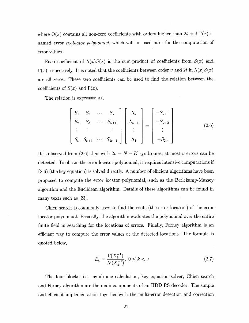
where 8(x) contains all non-zero coefficients with orders higher than 2t and 1(x) is
named error evaluator polynomial, which will be used later for the computation of
error values.
Each coefficient of A(x)S(x) is the sum-product of coefficients from S(x) and
1(x) respectively. It is noted that the coefficients between order v and 2t in A(x)S(x)
are all zeros. These zero coefficients can be used to find the relation between the
coefficients of S(x) and 1(x).
The relation is expressed as,
S 1 S2 ... Su AV -Sv+1
S2 S3 -. Sv+1 A-1 -Sv+2(26)
Sv Sv+1 -.. S2v-1 A1 -S2v
It is observed from (2.6) that with 2v = N - K syndromes, at most v errors can be
detected. To obtain the error locator polynomial, it requires intensive computations if
(2.6) (the key equation) is solved directly. A number of efficient algorithms have been
proposed to compute the error locator polynomial, such as the Berlekamp-Massey
algorithm and the Euclidean algorithm. Details of these algorithms can be found in
many texts such as [23].
Chien search is commonly used to find the roots (the error locators) of the error
locator polynomial. Basically, the algorithm evaluates the polynomial over the entire
finite field in searching for the locations of errors. Finally, Forney algorithm is an
efficient way to compute the error values at the detected locations. The formula is
quoted below,
r7(X)Ek= k) 0<k<v (2.7)
The four blocks, i.e. syndrome calculation, key equation solver, Chien search
and Forney algorithm are the main components of an HDD RS decoder. The simple
and efficient implementation together with the multi-error detection and correction
capability make Reed-Solomon codes commonly used FEC codes.
2.2 Channel model, signal-to-noise ratio and reli-
ability
The additive white Gaussian noise (AWGN) channel model is widely used to test
channel coding performance. To communicate a message m across an AWGN channel,
a desired codeword c = [co, ci, ... , cN-1 T (which conveys the message m) is selected
for transmission. The binary-input AWGN channels are considered, where each non-
binary symbol ci E F28 is first represented as a s-bit vector [ci,o, - - , ci>s1]T before
transmission. Each bit ciy is then modulated (via binary phase shift keying) to xij
and xij = 1 - 2 - cij. Then xi,j is transmitted through the AWGN channel. Let
rij denote the real-valued channel observation corresponding to cij. The relation
between rij and cij is,
rij= z xy + nij (2.8)
where nij is Gaussian distributed random noise.
The power of modulated signal x is d2 if the value of zij is d or -d. In AWGN
channel, any nij in the noise vector n are independent and identically distributed
(IID). Here n is a white Gaussian noise process with a constant power spectral density
(PSD) of No/2. The variance of each nij is consequently o2 = No/2. If the noise
power is set to a constant 1, then No = 2.
In the measurement of decoder performance Eb/No is usually considered for the
signal to noise ratio, where Eb is the transmitted energy per information bit. Consider
a (N, K) block code. With an N-bit codeword, a K-bit message is transmitted.
In the above-mentioned BPSK modulation, the energy spent on transmitting the
information bit is Nd2/K. With the noise level of No = 2, the signal to noise ratio is
computed as
Eb -Nd 2 (2.9)
No 2K
Using Eb/No as the signal to noise ratio, we can fairly compare performance between
channel codes regardless of code length, rate or modulation scheme.
At the receiver, a symbol decision y!HD] c F 2, is made on each transmitted symbol
ci (from observations ri,0,- , ri,s_1). We denote y[HD} HD] HD] D]N as
the vector of symbol decisions.
Define the i-th symbol reliability 7y (see [2]) as
7i min Iri, (2.10)o<j<s
where | denotes absolute value. The value 74 indicates the confidence on the symbol
decision yiHD]; the higher the value of gi, the more confident and vice-versa.
An HDD decoder works on the hard-decided symbol vector y[HD] and takes no
advantage on the reliability information of each symbol, which, on the other hand, is
the main contributor to the performance enhancement in an LCC decoder.
2.3 The LCC decoding algorithm
Put the N symbol reliabilities ,yo, -, - -,7N-1 in increasing order, i.e.
71 72 N '' (27iN1)
and denote the index set I A {ii, i 2 ,--- , i, pointing to the r/-smallest reliability
values. We term I to be the set of least-reliable symbol positions (LRSP). The idea
of Chase decoding is simply stated as follows: the LRSP set I points to symbol
decisions y!HD] that have low reliability, and are received in error (i.e. y HD] does not
equal the transmitted symbol ci) most of the time. In Chase decoding we perform 2"
separate hard decision decodings on a test vector set {y(i) : 0 < j < 27 }. Each y(J) is

constructed by hypothesizing secondary symbol decisions y 2HD] . HD] that differ
from the symbol decision values y[HD] 'HD]. Each y!2HD] is obtained from y!HD], by
complementing the bit that achieves the minimum in (2.10), see [2].
Definition 3. The set of test vectors is defined as the set
yi = y [HD] for i V Iy : (2.12)
y E f{y[HD] Y[ 2HD]} for i E I
of size 27. Individual test vectors in (2.12) are distinctly labeled y(0) 7y , y(27-1)
An important complexity reduction technique, utilized in LCC, is coordinate trans-
formation [8, 17]. The basic idea is to exploit the fact that the test vectors yU) differ
only in the r; LRSP symbols (see Definition 3). In practice r is typically small, and
the coordinate transformation technique simplifies/shares computations over common
symbols (whose indexes are in the complementary set of I) when decoding the test
vectors y(O), ... y(2 -1)
Similarly to the LRSP set I, define the set of most-reliable symbol positions
(MRSP) denoted J, where J points to the K-highest positions in ordering (2.11),
i.e., 7 {iN-K+1, *' , iN}. For any [N, K] RS code C, a codeword c[l'] (with coef-
ficients denoted c') can always be found such that c[i equals the symbol decisions
y[HD] over the restriction J (i.e. c - yjHD] for all i E J, see [23]). Coordinate
transformation is initiated by first adding cl'l to each test vector in (2.12), i.e. [8, 17]
y0j) = Y) + c[jj (2.13)
for all j E {0, ... , 2q - 1}. It is clear that the transformed test vector yk() has the
property that 99 0 for i E J. We specifically denote 7 to be the complementary
set of 3, and we assume that the LRSP set I C J (i.e. we assume rq < N - K).
The interpolation phase of the LCC, need only be applied to elements {i : i E j}
(see [28, 2]). Denote the polynomial v(x) f ]jE (x - ai).
Definition 4. The process of finding a bivariate polynomial Q0) (x, z) that satisfies
the following properties
i) Q(i)(ai,P)/1v(ai)) = 0 for all i E
ii) Q(i)(x, z) =qU (x) + z - qU(x)(j) N-K (z) KO
iv) deg q0 (x) < N-K and deg q() W N-K
is known as interpolation [28, 2].
Each bivariate polynomial Q(i) (x, z) in Definition 4 is found using Nielson's al-
gorithm; the computation is shared over common interpolation points1 [2]. Next,
a total of 27 bivariate polynomials Q() (x, z), are obtained from each Q() (x, z), by
computing
Q ((x, z) = v(x) - qf (x) + z -qfj (x) (2.14)
for all j E {0, ... , 2" - 1}. In the factorization phase, a single linear factor z+00)6(x)
is extracted from QW (x, z). Because of the form of QW)(x, z) in (2.14), factorization
is the same as computing
$($(x) Av(x)qf )(x)/qf )(x). (2.15)
However, instead of individually factorizing (2.15) for all 27 bivariate polynomi-
als Qi(x, z), Bellorado and Kavoid proposed a reduced complexity factorization
(RCF) technique [2] that picks up only a single bivariate polynomial Q) (x, z) |j, =
Q(P) (x, z) for factorization. The following two metrics are used in formulating RCF
(see [2])
df degqo(x) - {i :qf (a) = 0,i E } , (2.16)
df ) deg qi(x) - {i : qj (a') = 0, i E } . (2.17)
'The terminology points come from the Sudan algorithm literature [28]. A point is a pair (ai, yi),where yj E F2 is associated with the element a.
The RCF algorithm considers likelihoods of the individual test vectors (2.12) when
deciding which polynomial Q(P) (x, z) to factorize (see [2]). The RCF technique greatly
reduces the complexity of the factorization procedure, with only a small cost in error
correction performance [2].
Once factorization is complete, the last decoding step involves retrieving the es-
timated message. If the original message m is encoded via evaluation-map (see Defi-
nition 1), then the LCC message estimate m is obtained as
N-1
rni = Z ( + c -( )i (2.18)j=0
for all i E {, ... , K - 1}, where coefficients $ correspond (via (2.15) and Definition
4) to the RCF-selected Q(P)(x, z). The second term on the RHS of (2.18) reverses
the effect of coordinate transformation (recall (2.13)). If we are only interested in
estimating the transmitted codeword d, the LCC estimate 6 is obtained as
8j= $(X)() 1=,i + c4 (2.19)
for all i {O, ... N - 1}.
Following the above LCC algorithms, a number of architecture designs were pro-
posed for implementation. In Chapter 5, our design will be compared to that in [33],
which is a combination of two techniques, the backward interpolation [15] and the
factorization elimination technique [14]. In contrast to these proposed architectures
that provide architectural-level improvements based on the original LCC algorithm,
we obtain significant reductions in complexity through the tight interaction of the
proposed algorithmic and architectural changes.
Backward interpolation [15] reverses the effect of interpolating over a point. Con-
sider two test vectors y(j) and y(j') differing only in a single point (or coordinate). If
Q() (x, z) and Q(i') (x, z) are bivariate polynomials obtained from interpolating over
y(W) and y(j'), then both Q(J)(x, z) and Q(W')(x, z) can be obtained from each other by a
single backward interpolation, followed by a single forward interpolation [15]. Hence,
this technique exploits similarity amongst the test vectors (2.12), relying on the avail-
ability of the full set of test vectors. This approach loses its utility in situations where
only a subset of (2.12) is required, as in our test vector selection algorithm.
Next, the factorization elimination technique [14] simplifies the computation of
(2.19), however at the expense of high latency of the pipeline stage, which conse-
quently limits the throughput of the stage. Thus, this technique is not well suited for
high throughput applications. For this reason, we propose different techniques (see
Chapter 3) to efficiently compute (2.19). As shown in Chapter 5, with our combined
complexity reduction techniques, the factorization part occupies a small portion of
the system complexity.

28
Chapter 3
Algorithm Refinements and
Improvements
In this section we describe the three modifications to the original LCC algorithm [2],
which result in the complexity reduction of the underlying decoder architecture and
physical implementation.
3.1 Test vector selection
The decoding of each test vector y(j), can be viewed as searching an N-dimensional
hypersphere of radius L(n - k + 1)/2] centered at y(j). In Chase decoding, the de-
coded codeword is therefore sought in the union of all such hyperspheres, centered
at each test vector y(j) [30]. As illustrated in Figure 3-1, the standard test vector
set in Definition 3 contains test vectors extremely close to each other, resulting in
large overlaps in the hypersphere regions. Thus, performing Chase decoding with the
standard test vector set is inefficient, as noted by F. Lim, our collaborator from UH
at Manoa.
In hardware design each test vector y(i) consumes significant computing resources.
For a fixed budget of h < 27 test vectors, we want to maximize the use of each test
vector y(i). We should avoid any large overlap in hypersphere regions. We select the
h test vectors y(i) as proposed by Tokushige et. al. [30]. For a fixed r, the h test
Test Vector Selection
y(O) YkU~~(2)
Sy( 3) is selectedas most-likely pointoutside shaded region
Figure 3-1: Simple q = 3 example to illustrate the difference between the standardChase and Tokushige et. al. [30] test vector sets. The standard Chase test vector set
has size 2 = 8. The Tokushige test vector set covers a similar region as the Chase,however with only h = 4 test vectors.
vectors y(), ... , y(-1) are selected from (2.12). The selection rule is simple: choose
the j-th test vector y(i), as the most-likely candidate in the candidate set, excluding
all candidates that fall in previously searched j - 1 hyperspheres.
The Tokushige test vector set is illustrated in Figure 3-1 via a simple example. The
test vector y(O) is always chosen as y(O) = y[HD]. Next, the test vector y(') is also chosen
from the candidate set (2.12). However, y(l) cannot be any test vector in (2.12), that
lies within the hypersphere centered at y(O). To decide amongst potentially multiple
candidates in (2.12), we choose the test vector with the highest likelihood. Similarly,
the next test vector y(2) is chosen similarly, i.e. y(2) is the most-likely candidate
outside of the two hyperspheres centered at y(O) and y(l) respectively. This is repeated
until all h test vectors y(j) are obtained.
The procedure outlined in the previous paragraph obtains a random choice of
test vectors. This is because the choice of each y() depends on the random likeli-
hoods. We repeat the procedure numerous times to finally obtain fixed test vectors
y(0) .. . , y(h-1), by setting each test vector y(i) to the one that occurs most of the time
(see [30]). In this method q and h are parameters that can be adjusted to obtain best
performance. Furthermore, we also let the hypersphere radius be an optimizable pa-
rameter. There is no additional on-line complexity incurred with the Tokushige test
vector set, the test vectors are computed off-line and programmed into the hardware.
In Figure 3-2, we compare the performances of both the standard Chase and
Standard Chase
10-20
0
6.5
SNR [dB]
Figure 3-2: Performance of test vector selection method for RS[255, 239,17].
Tokushige et. al. test vector sets, for the RS[255, 239, 17] code. To compare with
standard Chase decoding, we set the parameters (h = 24, r/ = 8) and (h = 25, r = 10).
It is clear that the Tokushige test vector set outperforms Chase decoding. In fact,
Tokushige's method with h = 2' and h = 25 achieves standard Chase decoding
performance with 2" = 25, and 2n = 26 respectively, which is equivalent to a com-
plexity reduction by a factor of 2. We also compare with the performance of the
Koetter-Vardy algorithm; we considered both multiplicity 5 and the (asymptotic)
infinite multiplicity cases. As seen in Figure 3-2, our LCC test cases perform in-
between both Koetter-Vardy algorithms. In fact when h = 2 , the Tokushige test
vector set performs practically as well as Koetter-Vardy with (asymptotically) infi-
nite multiplicity (only 0.05 dB away). This observation emphasizes that the LCC
is a low-complexity alternative to the Koetter-Vardy (which is practically impossi-
ble to build in hardware). Finally, we also compare our performance to that of the
Jiang-Narayanan iterative decoder [11], which performs approximately 0.5 dB better
than the LCC. However, do note that the complexity of the iterative decoder is much
higher than our LCC (see [11]).
3.2 Reshaping of the factorization formula
Factorization (2.15) involves 3 polynomials taken from the selected polynomial (P) (x, z)
(see (2.14)), namely q #3(x) and q," (x), and v(x) = HJ (x - a). The term v(x) is
added to reverse the effect of coordinate transformation, which is an important com-
plexity reduction technique for LCC. The computation of v(x) involves multiplying
K linear terms, which is difficult to do efficiently in hardware due to the relatively
large value of K (more details are given in Chapter 4 on the hardware analysis).
Note that the factorization (2.15) (only computed once with j = p when using
RCF) can be transformed to
q#() -X (N_
6(P)(z) q= (3.1)
where e(x) is a degree N-K polynomial satisfying v(x)e(x) = zN 1. The computa-
tion of e(x) involves multiplying only N - K linear terms, much fewer than K terms
for v(x). The polynomial product q0f)(x)- (xN - 1) is easily computed, by duplicating
the polynomial q") (x) and inserting zero coefficients. In addition, all 3 polynomials
q0 9(x), q!j')(x) and e(x) in (3.1) have low degrees of at most N - K, thus the large
latency incurred when directly computing v(x) is avoided. Ultimately the advantage
of the coordinate transformation technique is preserved.
3.3 Systematic message encoding
We show that the systematic message encoding scheme is more efficient than the
evaluation-map encoding scheme (see Definition 1), the latter used in the original
LCC algorithm [2]. If evaluation-map is used, then the final message estimate h is
recovered using (2.18), which requires computing the non-sparse summation involving
many non-zero coefficients c]. Computing (2.18) for a total of K times (for each
mi) is expensive in hardware implementation.
On the other hand if systematic encoding is used, then (2.19) is essentially used
to recover the message m, whose values mi appear as codeword coefficients ci (i.e.
ci = mi for i E {o, ... , K - 1}). A quick glance at (2.19) suggests that we require N
evaluations of the degree K - 1 polynomial 0) (x). However, this is not necessarily
true as the known sparsity of the errors can be manipulated to significantly reduce
the computation complexity.
As explained in [2], the examination of the zeros of qj2) (x) gives all possible MRSP
error locations (in J), the maximum number of which is (N - K)/2 (see Definition
4). In the worst-case that all other N - K positions (in 7) are in error, the total
number of possible errors is 3(N - K)/2. This is significantly smaller than K (e.g.
for the RS [255, 239,17], the maximum number of possibly erroneous positions is 24,
only a fraction of K = 239).
Systematic encoding also has the additional benefit of a computationally simpler
encoding rule. In systematic encoding, we only need to find a polynomial remain-
der [23], as opposed to performing the N polynomial evaluations in (2.1).

34
Chapter 4
VLSI Design of LCC Decoders
In this chapter, we describe the VLSI implementations of the full LCC decoders
based on the algorithmic ideas and improvements presented in previous sections,
mainly test-vector selection, reshaped factorization and systematic encoding. We
often use the LCC255 decoder with parameters (h = 24, 7 = 8) as the example for
explanation. The same design principle applies to LCC31 decoder with parameters
(h = 4, 7 = 6). In fact, most Verilog modules are parameterized and can be easily
adapted to a different RS decoder. All algorithm refinements and improvements
described in Chapter 3 are incorporated in the design. Further complexity reduction
is achieved via architecture optimization and cycle saving techniques.
The I/O interface and some chip design issues are presented in Appendix C.
Appendix D describes the main steps of the physical implementation and verification
of the VLSI design.
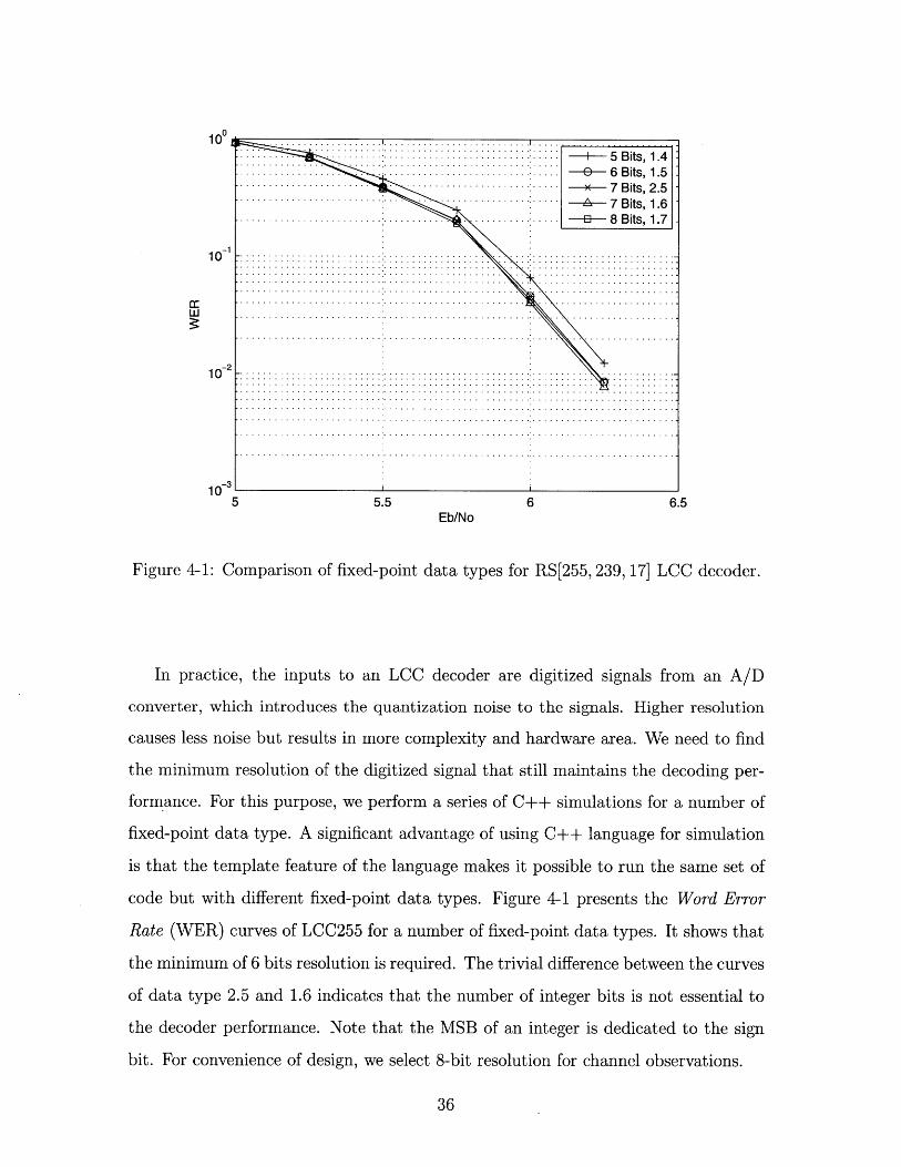
4.1 Digital signal resolution and C++ simulation
Before the VLSI design, we perform C++ simulation of the target decoders. There
are two reasons for the preparation work:
1. Decide the digital resolution of the channel observations.
2. Generate testing vectors for verification of each component of the VLSI design.
100
10
10-3 L5
Eb/No
Figure 4-1: Comparison of fixed-point data types for RS[255, 239, 17] LCC decoder.
In practice, the inputs to an LCC decoder are digitized signals from an A/D
converter, which introduces the quantization noise to the signals. Higher resolution
causes less noise but results in more complexity and hardware area. We need to find
the minimum resolution of the digitized signal that still maintains the decoding per-
formance. For this purpose, we perform a series of C++ simulations for a number of
fixed-point data type. A significant advantage of using C++ language for simulation
is that the template feature of the language makes it possible to run the same set of
code but with different fixed-point data types. Figure 4-1 presents the Word Error
Rate (WER) curves of LCC255 for a number of fixed-point data types. It shows that
the minimum of 6 bits resolution is required. The trivial difference between the curves
of data type 2.5 and 1.6 indicates that the number of integer bits is not essential to
the decoder performance. Note that the MSB of an integer is dedicated to the sign
bit. For convenience of design, we select 8-bit resolution for channel observations.
5 Bits, 1.4OE 6 Bits, 1.5 .
..... x 7 Bits, 2.5 -7 Bits, 1.6 ~
.--- 8 Bits, 1.7 -
-' - ' - -- - --- ----- - -N......
....................I . . . . .. . . . . . . . . .. . . . . . .. . .. ......................................
.. . .. . . . . . . . . . . . . . .. . . . . . . .. . . . . . . . . . .. . . . . . .. . .
................ .. ...............................
.. . .. . . . . . . . . . .. . . . . .. . . . . .. . . . . . . . . . .. . . . . . .. . .
.. . .. . . . . . . . . . .. . . . . . .. . .. . . . . . . . . .. . . . . . .. . .
.. . .. . . . . . . . . .. . . . . . . .. . . . . . . . . . . . . . .. . . . . . . .. . .
.. . .. . . . . . . . .. . . . . . . . .. . . . . . .. . . .. .. . . . . ...........
10-2........... ..............................
.............
..............
..............
...............
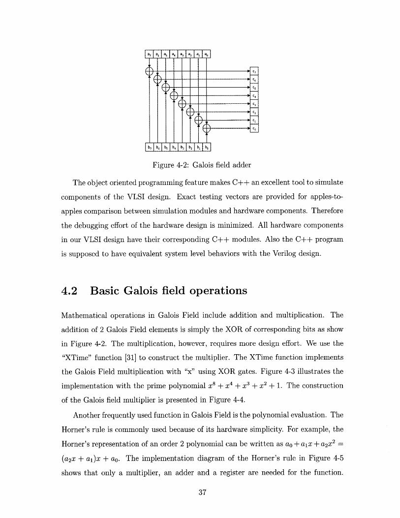
Figure 4-2: Galois field adder
The object oriented programming feature makes C++ an excellent tool to simulate
components of the VLSI design. Exact testing vectors are provided for apples-to-
apples comparison between simulation modules and hardware components. Therefore
the debugging effort of the hardware design is minimized. All hardware components
in our VLSI design have their corresponding C++ modules. Also the C++ program
is supposed to have equivalent system level behaviors with the Verilog design.
4.2 Basic Galois field operations
Mathematical operations in Galois Field include addition and multiplication. The
addition of 2 Galois Field elements is simply the XOR of corresponding bits as show
in Figure 4-2. The multiplication, however, requires more design effort. We use the
"XTime" function [31] to construct the multiplier. The XTime function implements
the Galois Field multiplication with "x" using XOR gates. Figure 4-3 illustrates the
implementation with the prime polynomial x8 + X4 + X3 + X2 + 1. The construction
of the Galois field multiplier is presented in Figure 4-4.
Another frequently used function in Galois Field is the polynomial evaluation. The
Horner's rule is commonly used because of its hardware simplicity. For example, the
Horner's representation of an order 2 polynomial can be written as ao + aix + a2x 2 =
(a2x + ai)x + ao. The implementation diagram of the Horner's rule in Figure 4-5
shows that only a multiplier, an adder and a register are needed for the function.
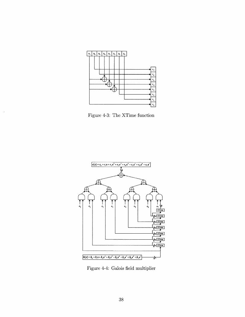
Figure 4-3: The XTime function
Figure 4-4: Galois field multiplier
Coefficients
Figure 4-5: Horner Scheme
a(x) D D ... D D
bib 1 b14 b15
A. Polynomial Multiplier
b13 F 14 b15 1/
ar D.D D
B. Polynomial Divider
Figure 4-6: Multiplication and Division of Galois Field Polynomials
For a polynomial of order N, it takes N + 1 cycles for the device to perform the
evaluation.
Polynomial multiplication and division are two frequently used polynomial oper-
ations in Galois Field. The implementation of polynomial multiplication takes the
form of an FIR filter where the coefficients of one polynomial pass through the FIR
filter constructed from the coefficients of the second polynomial. The polynomial
division, similarly, takes the form of IIR filter, i.e., the coefficients of the dividend
polynomial pass through the IIR filter constructed from the coefficients of the divisor
polynomial. Their implementation diagrams are presented in Figure 4-6.
4.3 System level considerations
The throughput of LCC decoders is set to one F2. symbol per cycle. This throughput
is widely adopted for RS decoders. To maintain the throughput, in each cycle the
LCC decoder assembles s channel observations rj, 0 < j < s, corresponding to one
F28 symbol. To maximize the decoder data rate and minimize the hardware size, the
output
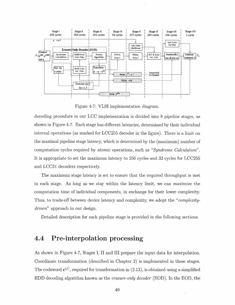
Stage I Stage II Stage Ill Stage IV256 cycles 169 cycles 1 161 cycles 1 98 cycles
Stage V Stage VI237 cycles 169 cycles
-PbytimeLikelihood
Erasure Only Decoder, (EOD),0:11Syndrome Build Error Forney Interp. Interp. RCF & Error Cact 0 (x) Calculation eval. Poly. A S 1 S
andy
i Sort by 1 Build Eras. Dadorn j
y re oc. PolY - y =equyn+ia
-- ---- Ray e(x)----------
Evaluate v(a 1). . . . . . . . .
forii Ef
iRC & ErrorJSort~~oc Codealc. 0[j
SI Sequential---- - - --- Reay , 2to l'arallel
Relayy~ y. . . . . . . ........I - ---
Figure 4-7: VLSI implementation diagram.
decoding procedure in our LCC implementation is divided into 8 pipeline stages, as
shown in Figure 4-7. Each stage has different latencies, determined by their individual
internal operations (as marked for LCC255 decoder in the figure). There is a limit on
the maximal pipeline stage latency, which is determined by the (maximum) number of
computation cycles required by atomic operations, such as "Syndrome Calculation".
It is appropriate to set the maximum latency to 256 cycles and 32 cycles for LCC255
and LCC31 decoders respectively.
The maximum stage latency is set to ensure that the required throughput is met
in each stage. As long as we stay within the latency limit, we can maximize the
computation time of individual components, in exchange for their lower complexity.
Thus, to trade-off between device latency and complexity, we adopt the "complexity-
driven" approach in our design.
Detailed description for each pipeline stage is provided in the following sections.
4.4 Pre-interpolation processing
As shown in Figure 4-7, Stages 1, 11 and III prepare the input data for interpolation.
Coordinate transformation (described in Chapter 2) is implemented in these stages.
The codeword cH, required for transformation in (2.13), is obtained using a simplified
HDD decoding algorithm known as the erasure-only decoder (EOD). In the EOD, the
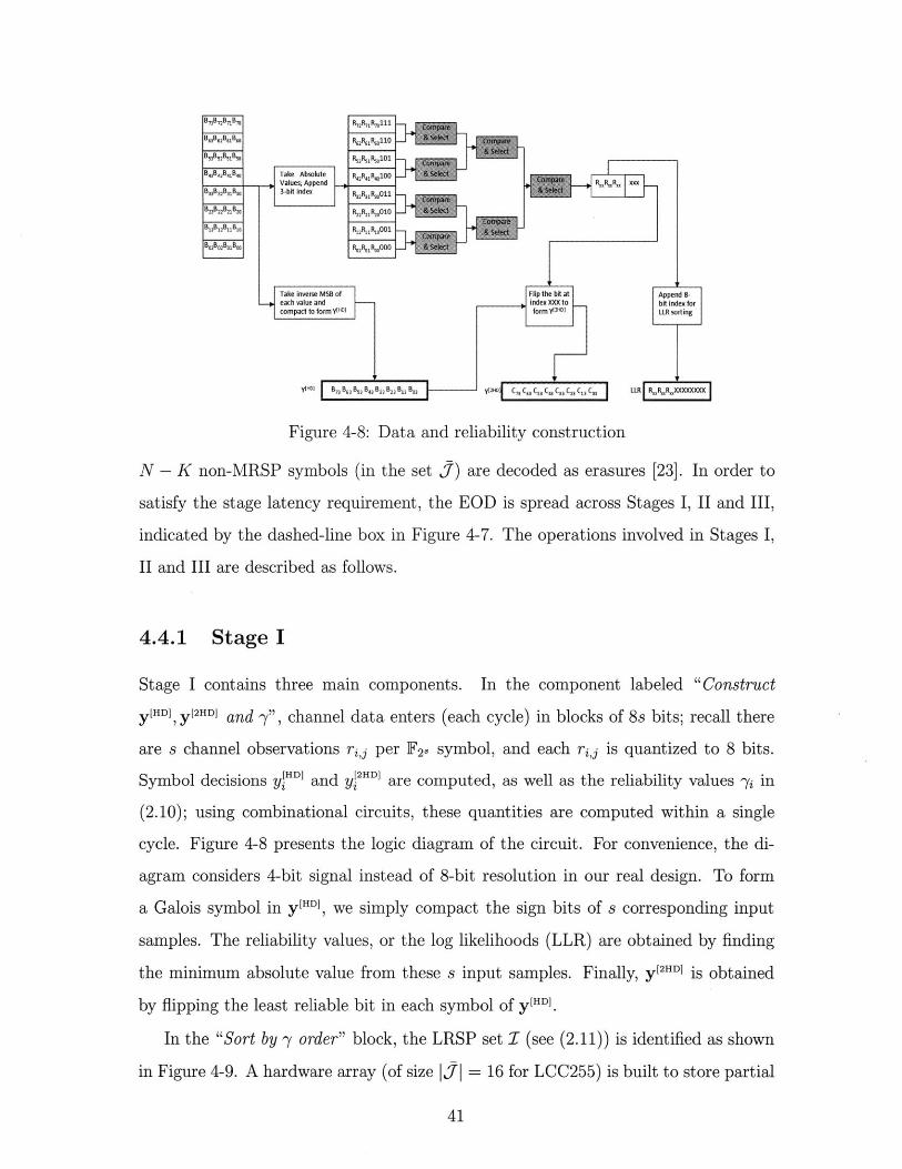
Figure 4-8: Data and reliability construction
N - K non-MRSP symbols (in the set T) are decoded as erasures [23]. In order to
satisfy the stage latency requirement, the EOD is spread across Stages 1, 11 and III,
indicated by the dashed-line box in Figure 4-7. The operations involved in Stages I,
II and III are described as follows.
4.4.1 Stage I
Stage I contains three main components. In the component labeled "Construct
y[HD] [2HD] and 7", channel data enters (each cycle) in blocks of 8s bits; recall there
are s channel observations rij per F2 1 symbol, and each rij is quantized to 8 bits.
Symbol decisions y HDI and y42
HD] are computed, as well as the reliability values -yj in
(2.10); using combinational circuits, these quantities are computed within a single
cycle. Figure 4-8 presents the logic diagram of the circuit. For convenience, the di-
agram considers 4-bit signal instead of 8-bit resolution in our real design. To form
a Galois symbol in y[HD], we simply compact the sign bits of s corresponding input
samples. The reliability values, or the log likelihoods (LLR) are obtained by finding
the minimum absolute value from these s input samples. Finally, y[ 2HD] is obtained
by flipping the least reliable bit in each symbol of y[HD].
In the "Sort by -y order" block, the LRSP set I (see (2.11)) is identified as shown
in Figure 4-9. A hardware array (of size jj = 16 for LCC255) is built to store partial
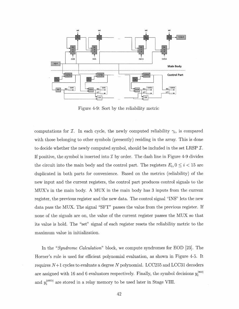
set set
Figure 4-9: Sort by the reliability metric
computations for I. In each cycle, the newly computed reliability 7j, is compared
with those belonging to other symbols (presently) residing in the array. This is done
to decide whether the newly computed symbol, should be included in the set LRSP I.
If positive, the symbol is inserted into I by order. The dash line in Figure 4-9 divides
the circuit into the main body and the control part. The registers Ej, 0 < i < 15 are
duplicated in both parts for convenience. Based on the metrics (reliability) of the
new input and the current registers, the control part produces control signals to the
MUX's in the main body. A MUX in the main body has 3 inputs from the current
register, the previous register and the new data. The control signal "INS" lets the new
data pass the MUX. The signal "SFT" passes the value from the previous register. If
none of the signals are on, the value of the current register passes the MUX so that
its value is hold. The "set" signal of each register resets the reliability metric to the
maximum value in initialization.
In the "Syndrome Calculation" block, we compute syndromes for EOD [23]. The
Horner's rule is used for efficient polynomial evaluation, as shown in Figure 4-5. It
requires N+1 cycles to evaluate a degree N polynomial. LCC255 and LCC31 decoders
are assigned with 16 and 6 evaluators respectively. Finally, the symbol decisions y HD]
and y 2HD] are stored in a relay memory to be used later in Stage VIII.
1 PD D ma D
a0 01 ak-1
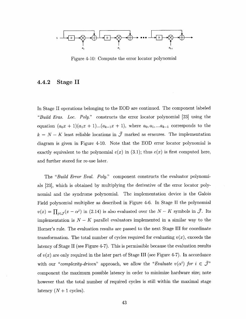
Figure 4-10: Compute the error locator polynomial
4.4.2 Stage II
In Stage II operations belonging to the EOD are continued. The component labeled
"Build Eras. Loc. Poly." constructs the error locator polynomial [23] using the
equation (aox + 1)(aix + 1)...(aklx + 1), where ao, ai, ...ak_1 corresponds to the
k = N - K least reliable locations in j marked as erasures. The implementation
diagram is given in Figure 4-10. Note that the EOD error locator polynomial is
exactly equivalent to the polynomial e(x) in (3.1); thus e(x) is first computed here,
and further stored for re-use later.
The "Build Error Eval. Poly." component constructs the evaluator polynomi-
als [23], which is obtained by multiplying the derivative of the error locator poly-
nomial and the syndrome polynomial. The implementation device is the Galois
Field polynomial multiplier as described in Figure 4-6. In Stage II the polynomial
v(x) = ] j (z - ai) in (2.14) is also evaluated over the N - K symbols in J. Its
implementation is N - K parallel evaluators implemented in a similar way to the
Horner's rule. The evaluation results are passed to the next Stage III for coordinate
transformation. The total number of cycles required for evaluating v(x), exceeds the
latency of Stage II (see Figure 4-7). This is permissible because the evaluation results
of v(x) are only required in the later part of Stage III (see Figure 4-7). In accordance
with our "complexity-driven" approach, we allow the "Evaluate v(a&) for i E "
component the maximum possible latency in order to minimize hardware size; note
however that the total number of required cycles is still within the maximal stage
latency (N + 1 cycles).
4.4.3 Stage III
In Stage III, the "Forney's algorithm" [23] computes the N - K erasure values.
After combining with the MRSP symbols in 5, we complete the clk codeword. The
N - K erasure values are also stored in a buffer for later usage in Stage VIII. The
complete c[H is further used in the component labeled " Transform yr = y + clJ]". The
computation of v(ai)-1 (see Definition 4) is also performed here (recall the evaluation
values of v(x) have already been computed in Stage II). Finally, the transformed values
(y[HD +C1) -)v(ai)1 and (Y 2HD} + _v(a)1 are computed for all i E .
The operations involved in this stage are Galois Field addition, multiplication and
division. The implementations of addition and multiplication are presented in Figure
4-2 and 4-4. Division is implemented in two steps. Firstly, the inverse of the divisor is
obtained with a lookup table. Then the lookup output is multiplied with the dividend
and the division result is obtained.
4.5 Interpolation
Stage IV and Stage V perform the critical interpolation operation of the decoder.
The interpolation operation over a single point is performed by a single interpolation
unit [2]. The optimization of interpolation units and the allocation of these devices are
two design aspects that ensure the accomplishment of the interpolation step within
the pipeline latency requirement.
4.5.1 The interpolation unit
Interpolation over a point consists of the following two steps:
PE: [Polynomial Evaluation] Evaluating the bivariate polynomial Q(x, z) (partially
interpolated for all preceding points, see [2]), over a new interpolation point.
PU: [Polynomial Update] Based on the evaluation (PE) result and new incoming
data, the partially interpolated Q(x, z) is updated (interpolated) over the new
point [2].
A. Direct Approach
~ C icycles-
SConditionL I Polynomial
B. Piggyback Approach
Figure 4-11: Direct and piggyback approaches for interpolation architecture design.
The PE step involves first evaluating both polynomials qO) (x) and ql) (x), be-
longing to Q (x, z) = qj (x) + z -qfj (x). Assume that both degrees deg qo(x) and
deg q,(x) are D. If both deg qo(x) and deg q,(x) are evaluated in parallel (using
Horner's rule), then evaluating Q(x, z) (in the PE step) requires a total of D + 1 cy-
cles. The PU step takes D +2 cycles for the update. If we adopt the direct' approach
shown in Figure 4-11.A, both PE and PU steps require a total of 2D + 3 cycles.
The order of PE and PU in the direct approach is the result of PU's dependence
on the conditions generated from PE since both belong to the same interpolation
point, see [2]. However, it is possible to perform PE and PU concurrently if the PE
step belongs to the next point. Figure 4-11.B shows our new piggyback architecture,
where the total cycle count is now reduced to D + 2 (almost a two-fold savings). In
this new architecture, PE is performed concurrently, as the PU step serially streams
the output polynomial coefficients. Note that dedicated memory units are allocated
for each interpolation units.
'Direct in the sense of causality (time dependence) of events, see [2].
Lastly, the latency of each interpolation unit is tied to the degrees deg qO) (x) and
deg ql) (x), which grow by (at most) one after each update. Note that it is best to
match each unit's operation cycles to the (growing) degrees of the polynomials qU) (X)
and ql) (x). This is argued as follows: the number of cycles required for performing D
updates, when estimated as the sum of the growing polynomial degrees (i.e. degrees
grow as 1, 2, 3, - - , D), equals the arithmetic sum D(D+1)/2. Compared to allocating
a fixed D number of cycles per update (corresponding to the maximum possible degree
value of both qf(x) and q )(x)), we see that our savings are roughly 50%.
Incorporating all the above considerations, we finalize our design of the interpo-
lation unit as presented in Figure 4-12. The input and output of the unit are loaded
from and saved to storage memories such as "Coeff. Storage" and "Cond. Storage" in
Figure 4-11. We design the device with optimized micro-pipeline architecture. Delay
registers are inserted for synchronization between pipeline stages and the reduction of
the critical path. New interpolation can start when part of the device is still process-
ing the last interpolation. Consequently, none of the device components idles during
processing and the minimum of processing cycles is achieved.
4.5.2 The allocation of interpolation units
We next describe the assignment of interpolation units in Stages IV and V. Recall
from Chapter 2 the test vector set (2.12) of size 27. With r = 8 (for LCC255) Figure
4-13 illustrates a tree representation for all the 27 = 28 - 256 test vectors in (2.12).
The tree has N - K = 16 levels (for each interpolated location in J, recall Definition
4). A path from the root to each bottom leaf corresponds to a test vector in (2.12) as
follows. The symbol locations in j\I are common to all test vectors; the last 8 levels
correspond to the q = 8 LRSP locations I. At each level, two child nodes originate
from an (upper-level) parent node, representing the two hypotheses yjHD] and yj2HD] for
i E I. The number in each node indicates the corresponding hypotheses, specifically
0 + y[HD] and 1 [ y!2HD}
From Figure 4-13, it is clear that all test vectors (paths) share interpolation op-
erations from levels 0 to 7. We divide the interpolation procedure into 2 pipeline
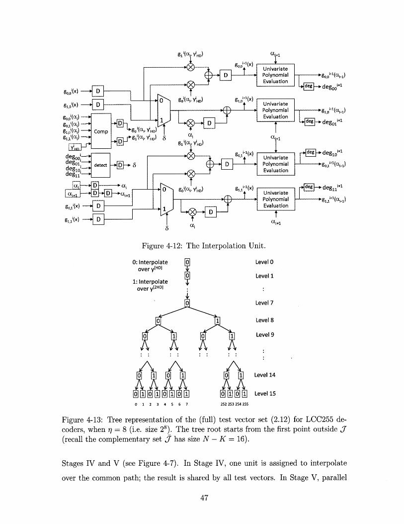
Figure 4-12: The Interpolation Unit.
0: Interpolate 0 Level 0over y[HD]
Level 11: Interpolate
over y[2HD]
0 Level 7
0 1Level 8
0 1 0 1 Level 9
0 1 0 1 0 1 Lee1
0 >0Level 14FO]L~ FI] F] F1 Levell15
0 1 2 3 4 5 6 7 252 253254255
Figure 4-13: Tree representation of the (full) test vector set (2.12) for LCC255 de-coders, when rq = 8 (i.e. size 2'). The tree root starts from the first point outside 3(recall the complementary set J has size N - K = 16).
Stages IV and V (see Figure 4-7). In Stage IV, one unit is assigned to interpolate
over the common path; the result is shared by all test vectors. In Stage V, parallel
0
[~1:0: 1J: :0: 1:1
220O 1 0 1, 0 1 0 1 i
33 41 1 0 10 11 1 12
01 01 1010 1010 0 10o1148 7
01 23 45 67 891011 1213 1415
0 1 0 1 3
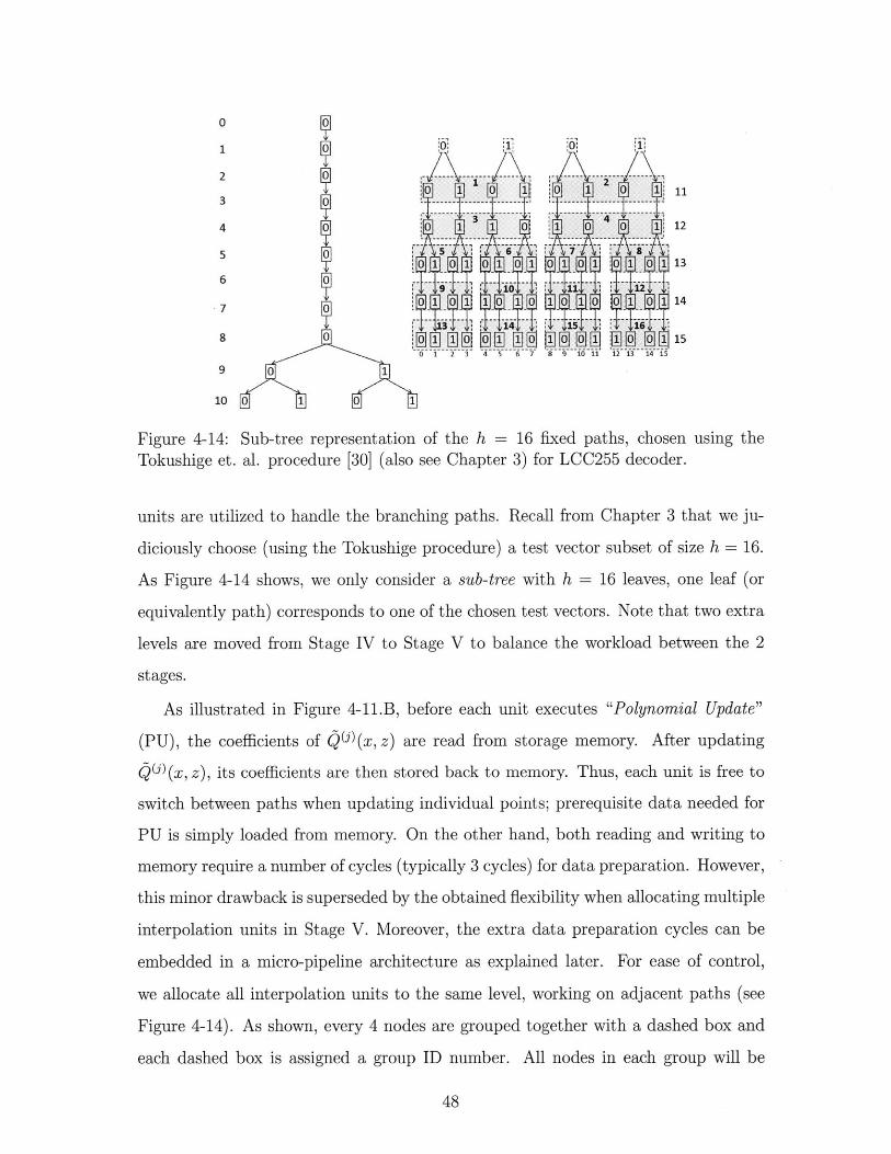
Figure 4-14: Sub-tree representation of the h = 16 fixed paths, chosen using theTokushige et. al. procedure [30] (also see Chapter 3) for LCC255 decoder.
units are utilized to handle the branching paths. Recall from Chapter 3 that we ju-
diciously choose (using the Tokushige procedure) a test vector subset of size h = 16.
As Figure 4-14 shows, we only consider a sub-tree with h = 16 leaves, one leaf (or
equivalently path) corresponds to one of the chosen test vectors. Note that two extra
levels are moved from Stage IV to Stage V to balance the workload between the 2
stages.
As illustrated in Figure 4-11.B, before each unit executes "Polynomial Update"
(PU), the coefficients of Q(i)(x, z) are read from storage memory. After updating
QMi)(x, z), its coefficients are then stored back to memory. Thus, each unit is free to
switch between paths when updating individual points; prerequisite data needed for
PU is simply loaded from memory. On the other hand, both reading and writing to
memory require a number of cycles (typically 3 cycles) for data preparation. However,
this minor drawback is superseded by the obtained flexibility when allocating multiple
interpolation units in Stage V. Moreover, the extra data preparation cycles can be
embedded in a micro-pipeline architecture as explained later. For ease of control,
we allocate all interpolation units to the same level, working on adjacent paths (see
Figure 4-14). As shown, every 4 nodes are grouped together with a dashed box and
each dashed box is assigned a group ID number. All nodes in each group will be
Time
Grp ID 1 3 5 9 13 11 3 0 6 10 14 2 4 7 11 15 2 4 8 12 16
on A. Depth-first ApproachSavings
Grp ID 9 2 4 | 8 10 11112 113 114|15|16
From parent From micro-
B. Breadth-first Approach sharmg pipehmng
Figure 4-15: Step 2 interpolation time line in the order of the sequence of group ID'sfor the depth-first and breadth-first approaches
processed in parallel using 4 interpolation units.
Figure 4-14 shows the assigned group ID's in the design. These groups are pro-
cessed in increasing order of the group ID's. From the assignment shown in Figure
4-14, it is clear that a tree level will be completed before proceeding onto the next
level. We term this approach the breadth-first approach. Alternatively, the groups
could have been processed, such that a set of tree paths will be completed, before pro-
ceeding onto the next set of tree paths. We wish to point out that the latter approach,
conversely termed the depth-first approach, has the following two disadvantages com-
pared to the former. Firstly, the depth-first approach breeds data dependency. If a
single interpolation unit works on a single path from the beginning to the end, the
PU for the current point has the following dependency on the previously updated
point. The memory read required to load the data for the current PU, is constrained
to happen only after the memory write is completed for the previously updated point.
The breadth-first approach on the other hand, will not have this constraint; consecu-
tively interpolated points always belong to different paths. By using a micro-pipeline
that has been set-up amongst the interpolation units, we are able to save the cycles
originally required for data preparation (we use a dual-port memory that permits
concurrent read/write). Without the micro-pipeline, the maximum number of cycles
required per interpolation (for the last node in a path), including the data preparation
cycles, is estimated as 17 + 3 = 20 cycles (3 cycles for data processing). A conserva-
tive estimate of the cycle savings is thus given as 3/20 = 0.15 (or 15%). The average
savings are actually higher because the number of cycles required by the other nodes
0
1
2
3 0
4 10
5 1 0 1 0
Figure 4-16: Sub-tree representation of the h = 4 fixed paths for RS [31, 25, 7] decoder.
is less than 17.
The second advantage of the breadth-first approach is that computations of the
parent nodes can be easily shared by their children. This is clearly difficult in the
depth-first approach, because in this case the intermediate results (from parent nodes
that are shared by children nodes) need to be stored in large amount of memory.
Hence to avoid storing intermediate results in the depth-first approach, we need to
perform these computations more than once. Figure 4-15 presents the interpola-
tion time line for both breath- and depth-first approaches, as well as illustrates the
pipelining effect. Out of the 20 operations required in the depth-first approach, 4 of
these operations are saved in the breadth-first approach, thus accounting for 20% sav-
ings. The total combined savings achieved by pipelining, and sharing of intermediate
results, are at least 32% in the breadth-first approach.
For LCC31 decoder, the assignment of interpolation units is presented in Figure
4-16. Level 0, 1, 2, 3 are processed in Stage IV with one interpolation unit. Level 4
and 5 are processed in Stage V with 2 parallel interpolation units.
4.5.3 Design techniques for interpolation stages
We summarize our cycle saving techniques in the interpolation phase and the saving
percentage for the LCC255 decoder as follows
1. The piggyback design of both PU and PE within the interpolation unit achieves

roughly 50% cycle reduction.
2. Tying-up interpolation cycles to the polynomial degrees deg qOU) (x) and deg qU) (x)
can achieve around 50% cycle reduction.
3. Breadth-first interpolation achieves a further cycle reduction of at least 32%.
The cycle savings reported above are approximations; values that are more accurate
are given in Chapter 5. Cycle savings translate into complexity savings when we
further apply our "complexity-driven" approach. The minimum number of required
interpolation units for Stage V of LCC255, in order to meet our latency requirement,
is reduced down to 4. For the LCC31 decoder, 2 interpolation units are required in
its Stage V.
The design flexibility introduced in sub-section 4.5.1 makes it possible to design a
generic interpolation processor as described in Figure 4-11.B, which can be configured
to meet various interpolation requirements. This is indeed how we design Stage IV
and Stage V for LCC255 and LCC31 decoders respectively, 4 scenarios in total. The
generic interpolation processor can be configured with the following parameters:
1. Number of parallel interpolation units
2. Number of test vectors for interpolation
3. Number of interpolation levels
4. The maximum degree of polynomials after interpolation
The coefficient storage memory in the processor can be configured with the same set
of parameters accordingly. Parameter 1 determines the bit width of the memory.
The depth of the memory is determined by the formula Parameter2/Parameter1 x
Parameter4. The coefficient memory is naturally divided into Parameter2/Parameterl
segments. Each segment contains the coefficients of a group of test vectors and they
will be processed in parallel by the same number of interpolation units, as shown in
Figure 4-14. Similar design applies to the condition storage in Figure 4-11.B. In the

end, we are able to use one generic design to cover Stage IV and Stage V for both
LCC255 and LCC31 decoders.
Besides the design flexibility, the operation of a designed interpolator is also flex-
ible. In each step of operation, the interpolation processor is instructed to fetch data
from the specified memory segment. The data are fed to the parallel interpolation
units together with other inputs such as the conditions and the test vector data for
the current interpolation point. The outputs of the interpolation units are also in-
structed to be saved in the specified memory segment. By controlling the target
read/write memory segments and the supplied test vector data, the operation of the
interpolation processor is fully programmable. These controls can be packed into a
sequence of control words that are used to program the interpolation function of the
device.
The flexibility of control words is essential to the support of the test vector se-
lection algorithm. As explained in Chapter 3, the test vector selection format is
determined to the type of transmission channel. The selection format must be pro-
grammable so the designed decoder can be adapted to match different types of trans-
mission channels. This adaptability is achieved by defining a specific sequence of
control words.
4.6 The RCF algorithm and error locations
We use LCC255 decoder for the explanation of Stage VI. The stage is divided into
2 phases. In phase 1, the RCF algorithm is performed so that a single bivariate
polynomial Q(P) (x, z) is picked up. In phase 2, the Chien search [23] is used to locate
the zeros of the polynomial q(P) (x). Recall that the zeros of qP) (x) correspond to
MRSP error locations in J (at most deg q(P) (x) < (N - K)/2 = 8 of them). Together
with the 16 non-MRSP locations J, there are a total of 24 possible error locations,
considered by Stage VII (which computes the 24 estimated (corrected) values).
Figure 4-17 illustrates the general procedure for the RCF algorithm [2]. The
interpolated bivariate polynomials Q) (x, z) are loaded from the "Storage Buffer".

Likelihoods
Figure 4-17: RCF block micro-architecture.
The metrics d(/) and dl (see (2.16) and (2.17)) are computed. The RCF chooses a
single bivariate polynomial Q(P) (x, z).
In accordance with the "complexity-driven" approach, the latency of the RCF
procedure is relaxed, by processing the 16 polynomials Q) (x, z), four at a time. As
compared to full parallel processing of all 16 polynomials, when we only process 4 at
a time, we reduce the hardware size by a factor of 4.
The "Compute Metrics" block (see Figure 4-17) dominates the complexity of Stage
VI. The main operation within this block, is to evaluate h = 16 polynomials qW (X),
each over - 16 values. This is to compute both RCF metrics d4' and dj in (2.16)
and (2.17). As mentioned before, there will be a total of 4 passes. In each pass, 4
bivariate polynomials will be evaluated in parallel, in half segments of |j|/2 = 8
values each. To this end, we build 32 polynomial evaluators, all implemented using
Horner's scheme as in Figure 4-5. Each pass will require a total of 20 cycles. The
computed metrics will then be passed over to the "RCF Algorithm" block and a
partial decision (for the final chosen Q(P) (x, z)) will be made based on the metrics
collected so far. The "Compute Metrics" block will dominate the cycle count in (Stage
VI) phase 1, and the total cycle count needed for all 4 passes is 80 cycles.
The selected polynomial Q(P) (x, z) from (Stage VI) phase 1, is brought over to
the second phase, for a Chien search. The same hardware for the 32 polynomial
evaluators (used in phase 1) is reused here for the Chien search. A total of 8 passes
will be required to complete the Chien search (testing all 255 unique F28 symbols).

Gfor 4 paths q0(x) = 0? OR flag
- Select indicator
dl for 4 paths comp.-- -- -- --- --
do for 4 paths comp
MIN dO'
icirnb2----------------w for 4 paths comp w=MAX(w)? comb3
MAX :w
Figure 4-18: Implementation diagram of the RCF algorithm.
Here in each pass, polynomial evaluation will require 10 cycles (the number of required
cycles equals deg q, (x)). Thus (Stage VI) phase 2 also requires a total of 80 cycles
(same as phase 1). Combining both phase 1 and phase 2 and including some overhead,
the latency of Stage VI is 169 cycles, which is within the maximum pipeline stage
latency (of 256 cycles).
The "RCF Algorithm" block in Figure 4-17 needs extra effort in design. Its
implementation diagram is presented in Figure 4-18. In order to meet the critical
path requirement, a number of delay registers are inserted, which turn the block into
a micro-pipeline system. The "comp" block compares the inputs and output logical
values. The "MIN" and "MAX" blocks find the minimum or maximum values of
the inputs. These two blocks introduce the main delays in critical paths. The dash
lines to "MIN" and "MAX" carry conditions that these blocks must satisfy when
performing their operations.
Finally, the "root collection" function collects the detected MRSP roots from the
8 passes of "Chien Search". In each pass, the "Chien Search" tests 32 symbols in
Galois Field F28 and generates a 32-bit zero mask that records the testing results.
The device presented in Figure 4-19 collects these roots according to the information
contained in the 32-bit zero mask.

midMask1
OR~ IX X X X... X X Xl X]midMask2
new~pMask XR ++_+++
XX X X ... jX XjX X] selMask
32 Galois Feld -- |MX --- +theOne
Figure 4-19: Diagram for root collection.
"opMask" is initialized with all ones so all bits in the zero mask are considered for
root collection. Each time after a root is collected, its representation bit in the zero
mask is disabled by setting the corresponding bit in "opMask" to zero. "midMask1"
is the AND result of the zero mask and "opMask". "midMask2" ensures all bits
after the first "1" bit in midMask1 are set to "1". In "selMask" only the first "1"
bit in "midMask1" is kept and all other bits are set to "0". "selMask" is used to
control the MUX block so the corresponding F2s symbol is selected for collection. In
the mean time, "selMask" is XORed with "opMask" to generate "newOpMask" in
which the bit corresponding to the collected root is disabled. "opMask" is updated
with "newOpMask" in the next cycle. The AND of the zero mask and "newOpMask"
indicates whether all roots have been collected. If so, the operation for this pass is
done. The total number of operation cycles equals to the number of roots detected in
the zero mask. So the maximum number of cycles is 8 due to the maximum degree
of the selected polynomial Q(') (x, z).
4.7 Factorization and codeword recovery
The selected bivariate polynomial Q(P) (x, z), is factorized in Stage VII. As shown
in the (reshaped) factorization formula (3.1), the factorization involves two separate

gO(x)
g1(x)
Sort bye(x) temporal
order
MRSPRoots ComputeLRSP Tempora
locators tnie
Figure 4-20: Detailed implementation diagram of Stage VII.
polynomial divisions, by both polynomials qlP)(x) and e(x). The coefficients of e(x)
are relayed (by a memory buffer, see Figure 4-7) from Stage II. Here, polynomial
division is implemented as shown in Figure 4-6. Two of such divisions will be needed
(one each for both q (x) and e(x)).
The division output $(P)(x) (see (3.1)) will be obtained after completing the fac-
torization, and will be needed to compute the estimated values 2j (see (2.19)). Recall
that the LCC only needs to consider 3(N - K)/2 = 24 (for LCC255) symbol posi-
tions in which errors may occur; these 24 positions include (N - K)/2 = 8 MRSP
positions and all N - K = 16 LRSP positions. Computing h- requires two steps.
First, we need to evaluate $(P)(x) over values a, for values a' corresponding to the 24
identified positions. This is done using 24 polynomial evaluators operating on O(P) (X).
Secondly, the previously applied coordinate transform (see (2.13)) must be undone.
This is done in the following Stage VIII, by adding back the corresponding symbols
cli. Note that to facilitate Stage VIII, the 24 identified positions must be sorted
in temporal order. The implementation is the same as Figure 4-9 with the sorting
metric set to the time index of the error locations. The implementation diagram for
Stage VII is presented in Figure 4-20.
The following are the inputs to Stage VIII: i) the outputs of the previous Stage
VII. ii) the c1[1 values indexed by the set J (relayed from Stage III). iii) the hard-
decision vector y[HD] (relayed from Stage I). The operations in Stage VIII are listed
below:
1. Output in temporal order the elements in the vector y[HDI = [__HD] ** D]T
2. Check if the index i of the current output y HD], corresponds or not to one of
the 24 locations that require correction.
3. If the index i is identified to require correction, construct the estimated value
8j according to (2.19). Replace the element y!HD] using the estimate 84.
4.8 Configuration module
Each function component in the LCC design is maximally parameterized. They can
be adapted to other specifications if their parameters are configured appropriately.
This flexibility is "static" in the sense that these parameters are configurable in design
stage but can not be changed when the design is finalized. Another level of flexibility,
the "dynamic" flexibility, allows the hardware behavior to be controlled in real time
by parameters or a sequence of control data. Our interpolation stage is designed with
both of these levels of flexibility.
The decoder with "dynamic" flexibility must be sets up with those control words
and configuration parameters before operation. The configuration module is designed
to facilitate the set up procedure. Each configuration parameter has a dedicated ad-
dress, which must be provided before the parameter value is presented to the config-
uration module. The sequence of control words for interpolation can be written to a
single dedicated address. Based on the specified address, the configuration module
sets up the corresponding component in the decoder. In this way, the set up procedure
simply becomes the provision of control addresses and control words. The internal
configuration work is handled by the configuration module.
The configuration module is a small component of the design, but it significantly
simplifies the set up procedure of the decoders and supports the feature of "dynamic"
flexibility.

58
Chapter 5
Design Results and Analysis
We synthesize, and place-and-route our design using 90nm CMOS technology and run
post-layout simulations to obtain area, power and timing estimates (See Appendix
D for details). The circuit layouts of LCC255, LCC31 and the I/O interface are
presented in Figure 5-1 and the key metrics are listed in Table 5.1.
LCC decoder is a complexity-improving algorithm as compared to the standard
Chase. We use the LCC255 decoder for complexity analysis since RS [255, 239,17]
code is widely used in previous LCC research. The analysis is performed as fol-
lows. First, the complexity distribution is presented in terms of gate counts, and
we highlight the various complexity reductions obtained from the proposed algorith-
mic changes. Next, utilizing both post place-and-route area and power estimates, we
compare the decoding efficiency of our design, to that of a standard Chase decoder
(using the RS decoder design in [18]). This comparison will demonstrate that the
LCC algorithm indeed allows for a simple hardware design. Then we will compare
our design architecture with the architecture previously presented in [33].
Finally, we compare LCC255 and LCC31 decoders (as algorithms with different
decoding performance). Under combined conditions of throughput, latency and area,
we investigate the behavior of their energy costs with the scaled supply voltage. We
then also quantitatively show the cost of higher decoding performance.

1.048 mm
Figure 5-1: The circuit lay
0.511 mm L I
)ut of the LCC design
Table 5.1: Implementation results for the proposed LCC VLSI designDecoder LCC255 LCC31Technology 90nm CMOS 90nm CMOSPower Supply 1.2V 1.2VClock Frequency 333MHz 333MHzThroughput 2.5Gpbs 1.3GpbsLatency 1347 cycles 196 cyclesGate Count 375411 gates 95354 gatesArea 1.048 x 0.965 = 1.01mm 2 0.511 x 0.499 = 0.255mm 2
Power Consumption 166mW 45mWDecoding Energy-cost 67pJ/bit 34pJ/bit
5.1 Complexity distribution of LCC design
Table 5.2 presents the complexity and latency measurements of each stage of the
synthesized design. Although the synthesized design may not fully represent the
design complexity, we will use the figures shown in Table I, to highlight the relative
cost of different blocks and complexity improvements resulting from the algorithm
Y
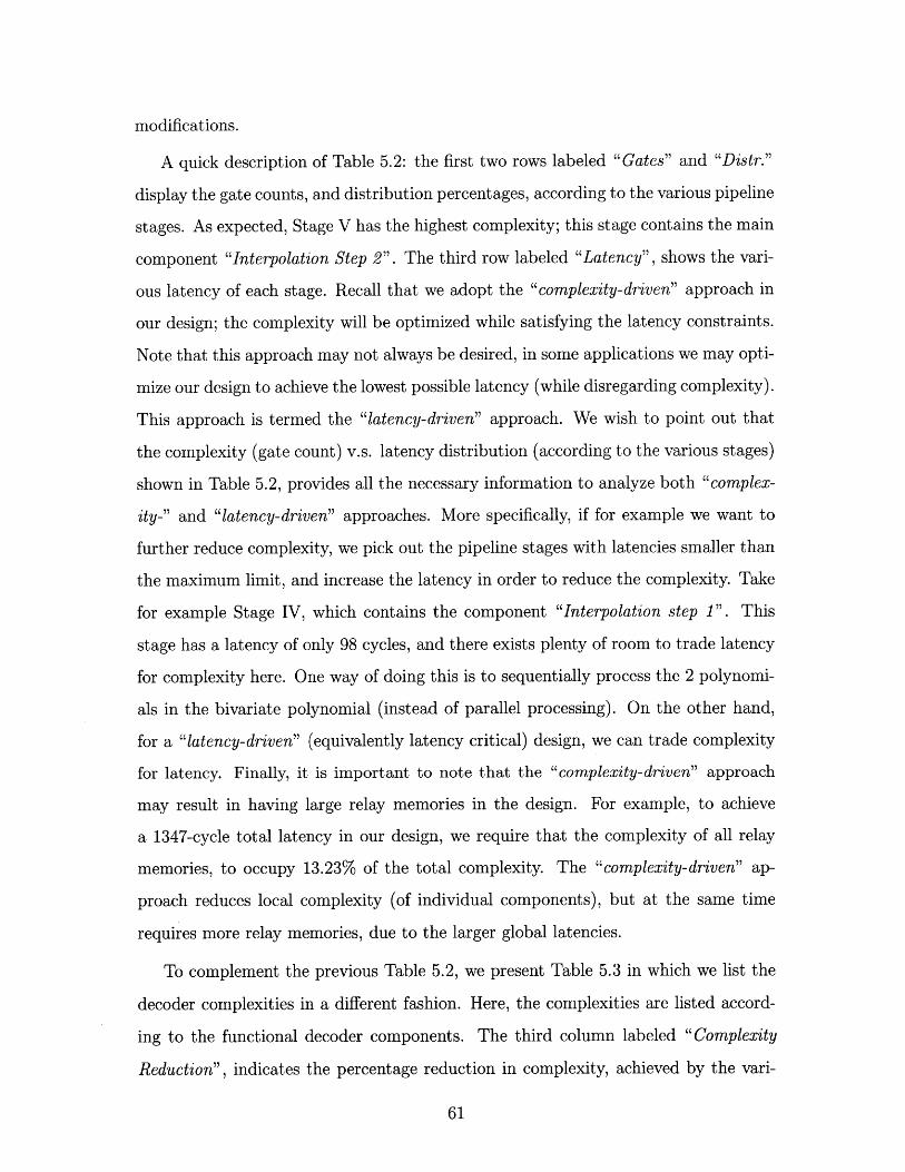
modifications.
A quick description of Table 5.2: the first two rows labeled "Gates" and "Distr."
display the gate counts, and distribution percentages, according to the various pipeline
stages. As expected, Stage V has the highest complexity; this stage contains the main
component "Interpolation Step 2". The third row labeled "Latency", shows the vari-
ous latency of each stage. Recall that we adopt the "complexity-driven" approach in
our design; the complexity will be optimized while satisfying the latency constraints.
Note that this approach may not always be desired, in some applications we may opti-
mize our design to achieve the lowest possible latency (while disregarding complexity).
This approach is termed the "latency-driven" approach. We wish to point out that
the complexity (gate count) v.s. latency distribution (according to the various stages)
shown in Table 5.2, provides all the necessary information to analyze both "complex-
ity-" and "latency-driven" approaches. More specifically, if for example we want to
further reduce complexity, we pick out the pipeline stages with latencies smaller than
the maximum limit, and increase the latency in order to reduce the complexity. Take
for example Stage IV, which contains the component "Interpolation step 1". This
stage has a latency of only 98 cycles, and there exists plenty of room to trade latency
for complexity here. One way of doing this is to sequentially process the 2 polynomi-
als in the bivariate polynomial (instead of parallel processing). On the other hand,
for a "latency-driven" (equivalently latency critical) design, we can trade complexity
for latency. Finally, it is important to note that the "complexity-driven" approach
may result in having large relay memories in the design. For example, to achieve
a 1347-cycle total latency in our design, we require that the complexity of all relay
memories, to occupy 13.23% of the total complexity. The "complexity-driven" ap-
proach reduces local complexity (of individual components), but at the same time
requires more relay memories, due to the larger global latencies.
To complement the previous Table 5.2, we present Table 5.3 in which we list the
decoder complexities in a different fashion. Here, the complexities are listed accord-
ing to the functional decoder components. The third column labeled "Complexity
Reduction", indicates the percentage reduction in complexity, achieved by the vari-
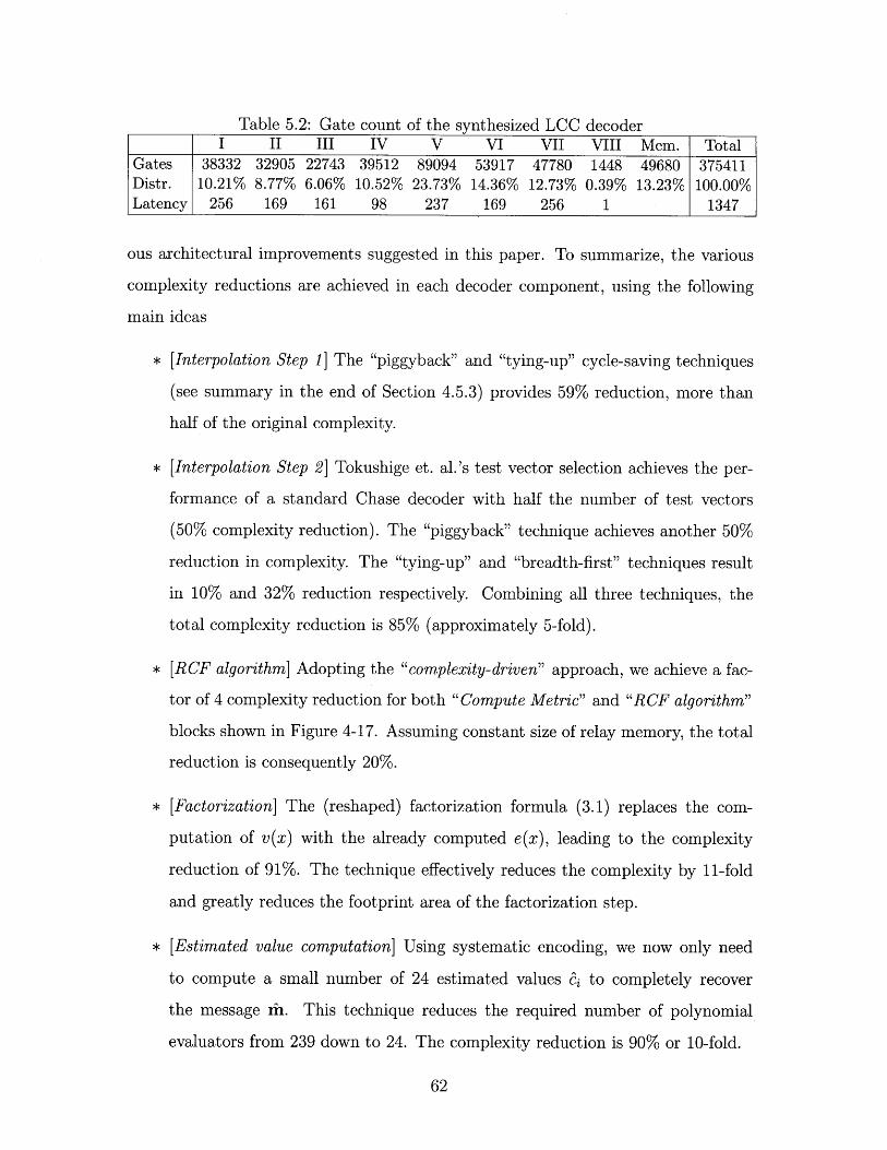
Table 5.2: Gate count of the synthesized LCC decoderI II III IV V VI VII VIII Mem. Total
Gates 38332 32905 22743 39512 89094 53917 47780 1448 49680 375411Distr. 10.21% 8.77% 6.06% 10.52% 23.73% 14.36% 12.73% 0.39% 13.23% 100.00%Latency 256 169 161 98 237 169 256 1 1347
ous architectural improvements suggested in this paper. To summarize, the various
complexity reductions are achieved in each decoder component, using the following
main ideas
* [Interpolation Step 1] The "piggyback" and "tying-up" cycle-saving techniques
(see summary in the end of Section 4.5.3) provides 59% reduction, more than
half of the original complexity.
* [Interpolation Step 2] Tokushige et. al.'s test vector selection achieves the per-
formance of a standard Chase decoder with half the number of test vectors
(50% complexity reduction). The "piggyback" technique achieves another 50%
reduction in complexity. The "tying-up" and "breadth-first" techniques result
in 10% and 32% reduction respectively. Combining all three techniques, the
total complexity reduction is 85% (approximately 5-fold).
* [RCF algorithm] Adopting the "complexity-driven" approach, we achieve a fac-
tor of 4 complexity reduction for both "Compute Metric" and "RCF algorithm"
blocks shown in Figure 4-17. Assuming constant size of relay memory, the total
reduction is consequently 20%.
* [Factorization] The (reshaped) factorization formula (3.1) replaces the com-
putation of v(x) with the already computed e(x), leading to the complexity
reduction of 91%. The technique effectively reduces the complexity by 11-fold
and greatly reduces the footprint area of the factorization step.
* [Estimated value computation] Using systematic encoding, we now only need
to compute a small number of 24 estimated values e4 to completely recover
the message i. This technique reduces the required number of polynomial
evaluators from 239 down to 24. The complexity reduction is 90% or 10-fold.
Table 5.3: Complexity Distribution of the synthesized LCC decoder
Gates Distr. ComplexityReduction
Hard Decision and Reliability 34040 9.07%Erasure Only Decoder 31593 8.42%Coordinate Transformation 28347 7.55%Interpolation Step 1 39512 10.52% 59%Interpolation Step 2 89094 23.73% 85%RCF Algorithm 53917 14.36% 20%Factorization 12733 3.39% 91%Corrected value computation 13680 3.64% 90%Codeword Recovery 22815 6.08%Relay Memory 49680 13.23%Total 375411 100.00% 70%
Our new algorithmic modifications and architecture design are justified by an
overall complexity reduction of 70%. The complexities of the core components (e.g.
interpolation, RCF, Factorization, and estimated value computation) are reduced by
80%. These components now only occupy 56% of the whole design, as opposed to 86%
of the original algorithm (suggested in [2]). In our improved design, these components
no longer dominate design complexities, and future efforts should be directed toward
reducing the complexities of other infrastructure components (that had negligible
contribution so far).
Figure 5-2 shows the (projected) complexity distributions versus the number of
test vectors h. It is clear that only the "Interpolation Step 2" and "RCF Algorithm"
component complexities (see Table 5.3) depend on h; the other components do not
vary when h is changed. Therefore as Figure 5-2 shows, both components "Inter-
polation Step 2" and "RCF Algorithm" eventually dominate the decoder complexity
for large enough h. To investigate the trade-off between increased performance and
complexity for a larger h, we observe the following from both Figures 3-2 and 5-2.
When comparing cases h = 16 and h = 32, we notice diminishing returns in perfor-
mance increment (see Figure 3-2), however the complexity increase is much sharper
(see Figure 5-2). We find that h = 16 is a reasonable choice for the number of test
vectors.
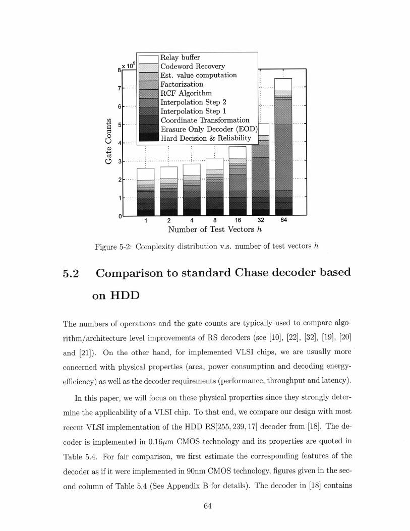
Relay buffer
8 < Codeword RecoveryEst. value computationFactorizationRCF Algorithm
6 -...- Interpolation Step 2 of tsvosInterpolation Step 1
5C--.. Coordinate Transformationre l Erasure Only Decoder (EODs
4oc...0.- Hard Decision & Reliability
4 1.... 2.4.8.1
effcinc)usrella 5-2: Coeit dreutins. roneroutpvetor anaec)
In.hi Coper ar ilfson the hsialprtieh s se teyongly daeed
mine thmer ofpoerabtyon andLS chipeT gtha eond, aretyialsd compare oualgg wt ot
recthm/archimptulevlpoementats h HDD RS25 37 decoder[1] [22], []1] The0]e
concerni mmned wihpyinalm MStchooy nt properties arepwrcnsmto n edn qenery
Table 5.4. For fair comparison, we first estimate the corresponding features of the
decoder as if it were implemented in 90nm CMOS technology, figures given in the sec-
ond column of Table 5.4 (See Appendix B for details). The decoder in [18] contains
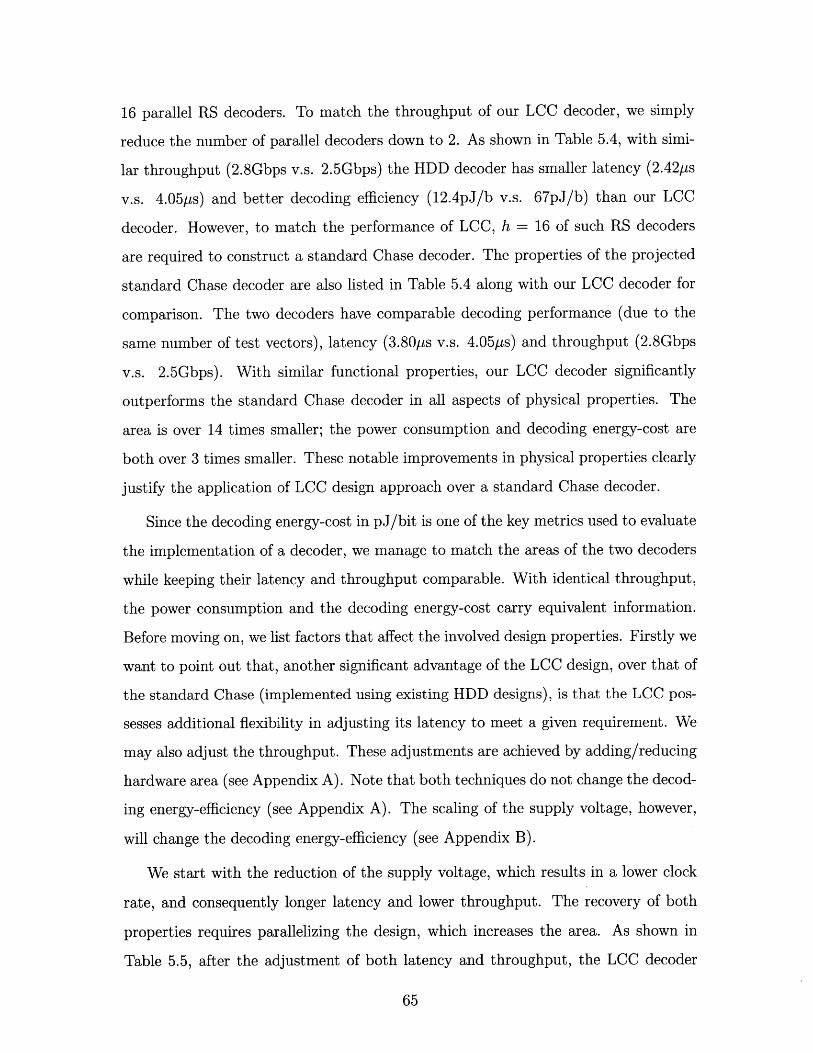
16 parallel RS decoders. To match the throughput of our LCC decoder, we simply
reduce the number of parallel decoders down to 2. As shown in Table 5.4, with simi-
lar throughput (2.8Gbps v.s. 2.5Gbps) the HDD decoder has smaller latency (2.42ps
v.s. 4.05ps) and better decoding efficiency (12.4pJ/b v.s. 67pJ/b) than our LCC
decoder. However, to match the performance of LCC, h = 16 of such RS decoders
are required to construct a standard Chase decoder. The properties of the projected
standard Chase decoder are also listed in Table 5.4 along with our LCC decoder for
comparison. The two decoders have comparable decoding performance (due to the
same number of test vectors), latency (3.80ps v.s. 4.05ps) and throughput (2.8Gbps
v.s. 2.5Gbps). With similar functional properties, our LCC decoder significantly
outperforms the standard Chase decoder in all aspects of physical properties. The
area is over 14 times smaller; the power consumption and decoding energy-cost are
both over 3 times smaller. These notable improvements in physical properties clearly
justify the application of LCC design approach over a standard Chase decoder.
Since the decoding energy-cost in pJ/bit is one of the key metrics used to evaluate
the implementation of a decoder, we manage to match the areas of the two decoders
while keeping their latency and throughput comparable. With identical throughput,
the power consumption and the decoding energy-cost carry equivalent information.
Before moving on, we list factors that affect the involved design properties. Firstly we
want to point out that, another significant advantage of the LCC design, over that of
the standard Chase (implemented using existing HDD designs), is that the LCC pos-
sesses additional flexibility in adjusting its latency to meet a given requirement. We
may also adjust the throughput. These adjustments are achieved by adding/reducing
hardware area (see Appendix A). Note that both techniques do not change the decod-
ing energy-efficiency (see Appendix A). The scaling of the supply voltage, however,
will change the decoding energy-efficiency (see Appendix B).
We start with the reduction of the supply voltage, which results in a lower clock
rate, and consequently longer latency and lower throughput. The recovery of both
properties requires parallelizing the design, which increases the area. As shown in
Table 5.5, after the adjustment of both latency and throughput, the LCC decoder
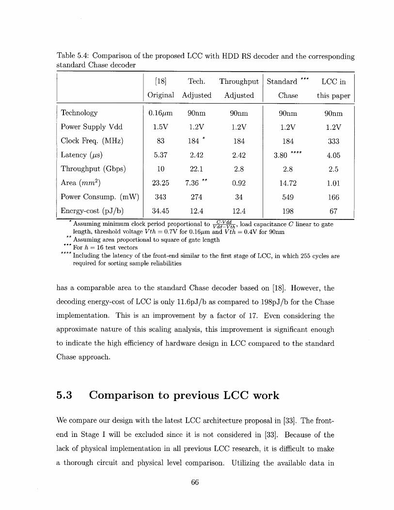
Table 5.4: Comparison ofstandard Chase decoder
the proposed LCC with HDD RS decoder and the corresponding
[18] Tech. Throughput Standard LCC in
Original Adjusted Adjusted Chase this paper
Technology 0. 16pm 90nm 90nm 90nm 90nm
Power Supply Vdd 1.5V 1.2V 1.2V 1.2V 1.2V
Clock Freq. (MHz) 83 184 * 184 184 333
Latency ([ps) 5.37 2.42 2.42 3.80 **** 4.05
Throughput (Gbps) 10 22.1 2.8 2.8 2.5
Area (mm 2 ) 23.25 7.36 ** 0.92 14.72 1.01
Power Consump. (mW) 343 274 34 549 166
Energy-cost (pJ/b) 34.45 12.4 12.4 198 67
* Assuming minimum clock period proportional to CyVdd load capacitance C linear to gateVdd-Vth'Ilength, threshold voltage Vth = 0.7V for 0.16pum and Vth = O.4V for 90nm
** Assuming area proportional to square of gate lengthFor h = 16 test vectorsIncluding the latency of the front-end similar to the first stage of LCC, in which 255 cycles arerequired for sorting sample reliabilities
has a comparable area to the standard Chase decoder based on [18]. However, the
decoding energy-cost of LCC is only 11.6pJ/b as compared to 198pJ/b for the Chase
implementation. This is an improvement by a factor of 17. Even considering the
approximate nature of this scaling analysis, this improvement is significant enough
to indicate the high efficiency of hardware design in LCC compared to the standard
Chase approach.
5.3 Comparison to previous LCC work
We compare our design with the latest LCC architecture proposal in [33]. The front-
end in Stage I will be excluded since it is not considered in [33]. Because of the
lack of physical implementation in all previous LCC research, it is difficult to make
a thorough circuit and physical level comparison. Utilizing the available data in
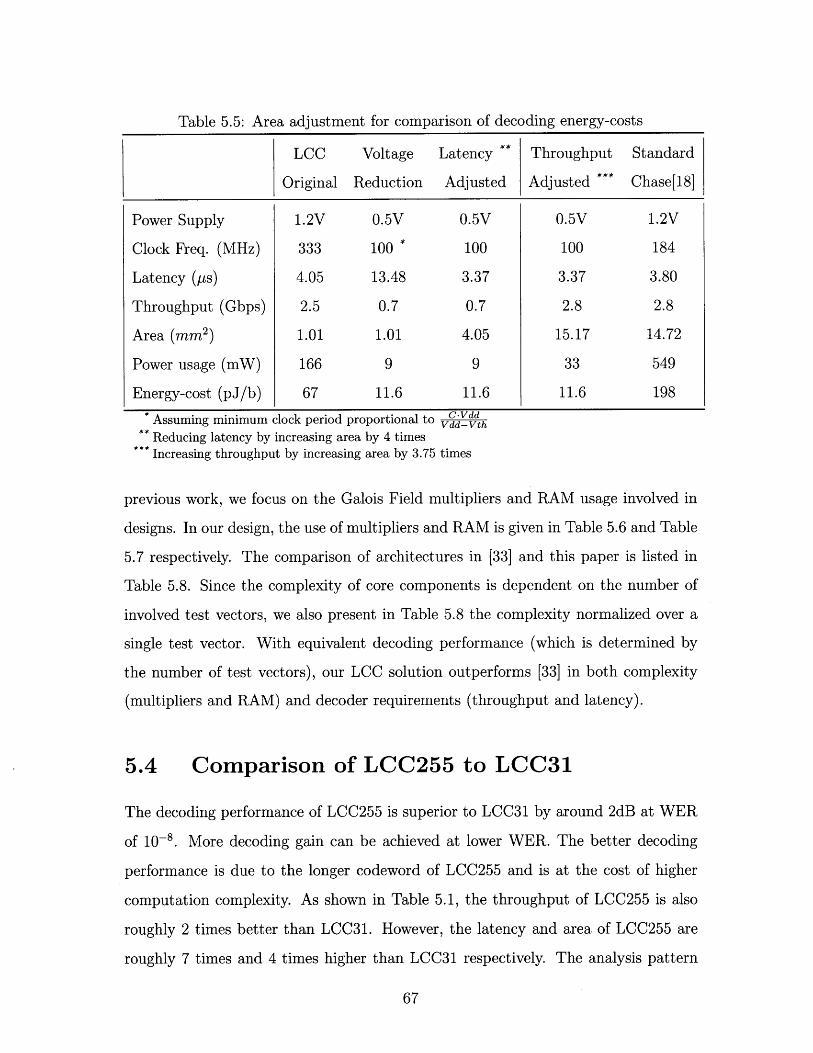
Table 5.5: Area adjustment for comparison of decoding energy-costs
LCC Voltage Latency ** Throughput Standard
Original Reduction Adjusted Adjusted Chase[18]
Power Supply 1.2V 0.5V 0.5V 0.5V 1.2V
Clock Freq. (MHz) 333 100 * 100 100 184
Latency (ps) 4.05 13.48 3.37 3.37 3.80
Throughput (Gbps) 2.5 0.7 0.7 2.8 2.8
Area (mm 2 ) 1.01 1.01 4.05 15.17 14.72
Power usage (mW) 166 9 9 33 549
Energy-cost (pJ/b) 67 11.6 11.6 11.6 198
* Assuming minimum clock period proportional to C.Vdd
** Reducing latency by increasing area by 4 timesIncreasing throughput by increasing area by 3.75 times
previous work, we focus on the Galois Field multipliers and RAM usage involved in
designs. In our design, the use of multipliers and RAM is given in Table 5.6 and Table
5.7 respectively. The comparison of architectures in [33] and this paper is listed in
Table 5.8. Since the complexity of core components is dependent on the number of
involved test vectors, we also present in Table 5.8 the complexity normalized over a
single test vector. With equivalent decoding performance (which is determined by
the number of test vectors), our LCC solution outperforms [33] in both complexity
(multipliers and RAM) and decoder requirements (throughput and latency).
5.4 Comparison of LCC255 to LCC31
The decoding performance of LCC255 is superior to LCC31 by around 2dB at WER
of 10-8. More decoding gain can be achieved at lower WER. The better decoding
performance is due to the longer codeword of LCC255 and is at the cost of higher
computation complexity. As shown in Table 5.1, the throughput of LCC255 is also
roughly 2 times better than LCC31. However, the latency and area of LCC255 are
roughly 7 times and 4 times higher than LCC31 respectively. The analysis pattern
Table 5.6: Multiplier usage in the proposed LCC decoderI Mult. [Notes
Syndrome (EOD)Location Poly. (EOD)Evaluation Poly. (EOD)v(x) evaluationForney (EOD)/TransformInterpolation Step 1Interpolation Step 2RCF/Chien searchFactorizationError computationTotal
162161651248322624
197
Calculation of EOD syndromes in Stage IConstruct location polynomial in Stage IIConstruct evaluation polynomial in Stage IIEvaluate v(x) for coordinate transformCompute cI'] and transform in Stage IIIOne interpolator has 12 multipliers4 parallel interpolation unitsZero checks of qi(x)9 an 17 mult. to divide qi(x) and e(x)Compute error values
Table 5.7: RAM usage in the proposed LCC decoderRAM (Bits) Notes
Stage IV 32x48 Memory storage for interpolation step 1Stage V 128x64 Memory storage for interpolation step 2Stage VI 64x36 Memory storage for interpolated coefficientsBuffer for e(x) 8x72 Relay memory of e(x) from Stage II to Stage VIIBuffer for y[HD] 8x1536 Relay memory of y[HD] from Stage I to Stage VIIITotal 24896
Table 5.8: Comparison of the proposed LCC archier and the work in [:331
in Section 5.2 can not be simply applied here because it is difficult to adjust their
throughputs, latencies and areas to same levels simultaneously. To compare the two
decoders, we first see how their energy costs change with throughputs as the supply
voltage ranges from 0.6V to 1.8V (see Appendix B for estimation models). The voltage
range is reasonable for a decoder designed and tested with 1.2V supply voltage.
As shown in Figure 5-3, both decoders have fast increasing energy costs as their
throughputs increase with the supply voltage. The behavior is expectable based on
the models presented in Appendix B. The energy cost of LCC31 quickly surpasses
Original Per test vector[33] This Work [33] This Work
Equivalent number of test vectors 8 32 1 1Latency (from input to output) 1995 1347 1995 1347Throughput (cycles per codeword) 528 256 528 256Number of Multipliers 74 197 9 6RAM Usage (Bits) 16928 24896 2116 778

Decoding Energy Cost v.s. Throughput
1000.
0 80
W 60
1.5 2Throughput (Gbps)
Figure 5-3: Decoding energy cost v.s. maximum throughput with supply voltageranging from 0.6V to 1.8V
LCC255 with limited improvements in throughput.
The scaling of the supply voltage not only changes the throughput but also the
latency. Both of them can be compensated with area (See Appendix A). Figure 5-4
presents the energy cost versus area curves for both decoders with areas adjusted to
maintain constant throughputs and latencies. The energy cost of LCC31 is signifi-
cantly lower than LCC255 in the overlapping range of the adjusted areas. Therefore,
with unchanged decoding performance, throughput and latency, and with matching
area sizes, LCC31 has an excellent property in decoding energy cost than LCC255.
Using the area adjustment techniques in Appendix A, we can first match both
decoders with equivalent throughputs and latencies. According to the models used
in our analysis (see Appendix B), the throughputs and latencies keep the equivalence
between both decoders as the supply voltage scales. Then we adjust the areas again
to restore the throughputs and latencies back to their level before voltage scaling.
In this way, we maintain the equivalence and consistence of the throughputs and
latencies throughout the scaling range of the supply voltage. In practice, it is more
convenient to match low throughput to high throughput (by adding area) and low
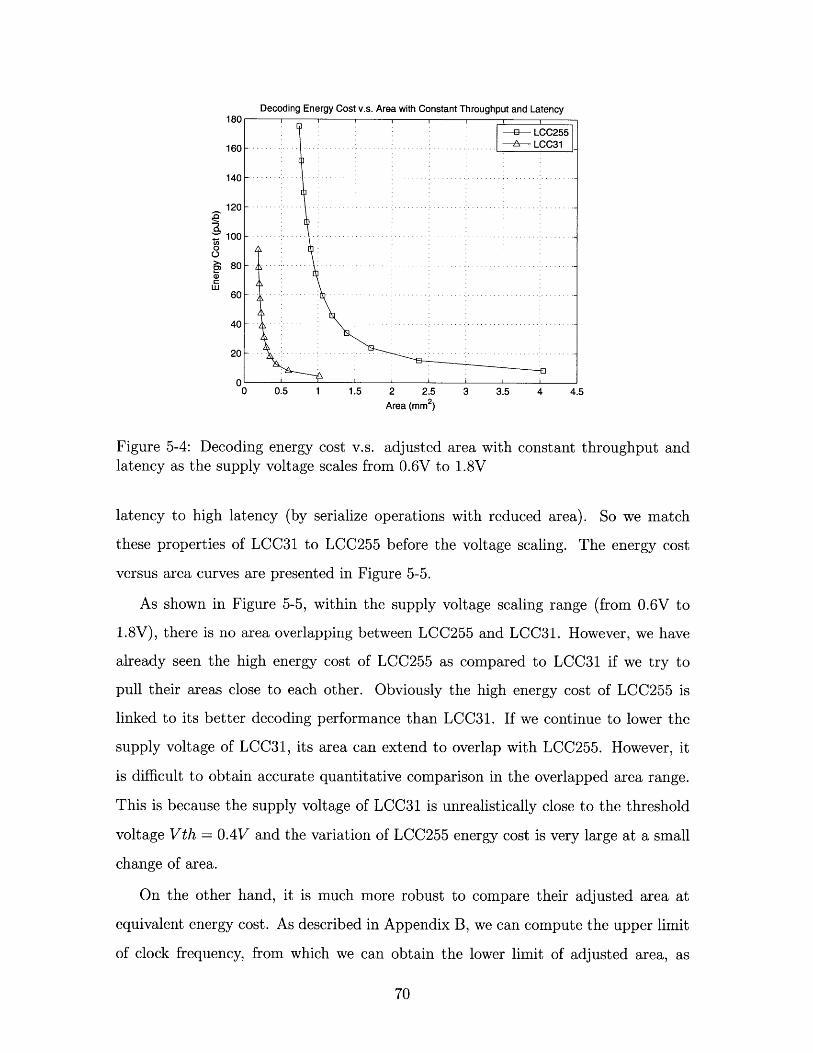
Decoding Energy Cost v.s. Area with Constant Throughput and Latency180
-a---LCC255
160 -- LCC31 _
140 -
120- - -
100-
80-
60-40
0 0.5 1 1.5 2 2.5 3 3.5 4 4.5Area (rnm 2)
Figure 5-4: Decoding energy cost v.s. adjusted area with constant throughput andlatency as the supply voltage scales from 0.6V to 1.8V
latency to high latency (by serialize operations with reduced area). So we match
these properties of LCC31 to LCC255 before the voltage scaling. The energy cost
versus area curves are presented in Figure 5-5.
As shown in Figure 5-5, within the supply voltage scaling range (from 0.6V to
1.8V), there is no area overlapping between LCC255 and LCC31. However, we have
already seen the high energy cost of LCC255 as compared to LCC31 if we try to
pull their areas close to each other. Obviously the high energy cost of LCC255 is
linked to its better decoding performance than LCC31. If we continue to lower the
supply voltage of LCC31, its area can extend to overlap with LCC255. However, it
is difficult to obtain accurate quantitative comparison in the overlapped area range.
This is because the supply voltage of LCC31 is unrealistically close to the threshold
voltage Vth = O.4V and the variation of LCC255 energy cost is very large at a small
change of area.
On the other hand, it is much more robust to compare their adjusted area at
equivalent energy cost. As described in Appendix B, we can compute the upper limit
of clock frequency, from which we can obtain the lower limit of adjusted area, as
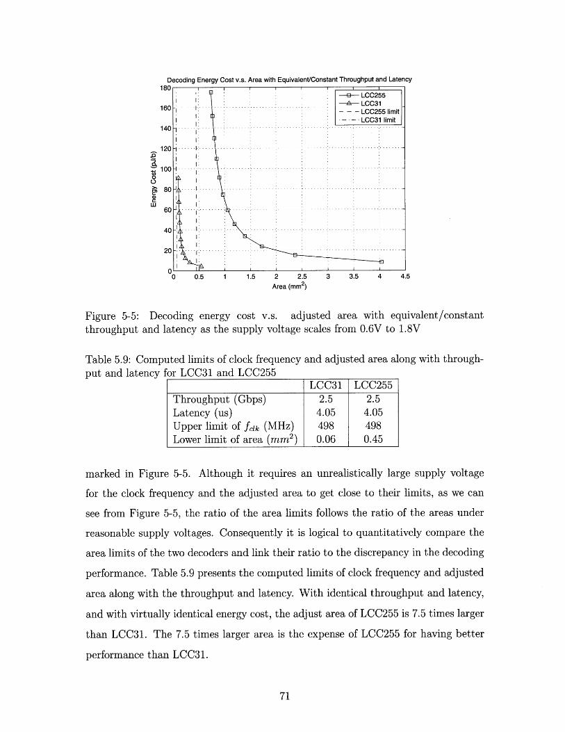
Decoding Energy Cost v.s. Area with Equivalent/Constant Throughput and Latency180
-B- LCC255-A- LCC31
1601 1 - - - LCC255 limit- -- - LCC31 limit
140 -1-
1201
100 -
0
> 801 0 .5 1.5 5 4 . 5
Ara mm60
Figure 5-5: Decoding energy cost v.s. adjusted area with equivalent /constantthroughput and latency as the supply voltage scales from 0.6V to 1.8V
Table 5.9: Computed limits of clock frequency and adjusted area along with through-put and latency for LCC31 and LCC255
LCC31 LCC255
Throughput (Gbps) 2.5 2.5
Latency (us) 4.05 4.05Upper limit Of ferk (MHz) 498 498Lower limit of area (mm2) 0.06 0.45
marked in Figure 5-5. Although it requires an unrealistically large supply voltage
for the clock frequency and the adjusted area to get close to their limits, as we can
see from Figure 5-5, the ratio of the area limits follows the ratio of the areas under
reasonable supply voltages. Consequently it is logical to quantitatively compare the
area limits of the two decoders and link their ratio to the discrepancy in the decoding
performance. Table 5.9 presents the computed limits of clock frequency and adjusted
area along with the throughput and latency. With identical throughput and latency,
and with virtually idt ec nergy cost, the adjust area of LCC255 is 7.5 times larger
than LCC31. The 7.5 times larger area is the expense of LCC255 for having better
performance than LCC31.

72
Chapter 6
Conclusion and Future Work
6.1 Conclusion
In this thesis, we present the first complete VLSI design of improved LCC decoders.
We show that cross-layer approach to system design, through interaction among the
algorithm design and underlying architecture and circuit implementation, can yield
the most significant improvements in design complexity.
At the algorithmic level we first propose the test vector selection algorithm that
reduces the complexity of the LCC decoder proposed in [2]. We further propose the
reshaping of the factorization formula as well as the application of systematic message
encoding, in order to avoid the negative impact of the involved parts on previously
proposed complexity reduction techniques.
To support these algorithm improvements, we present a new VLSI design architec-
ture and apply it to the design of two decoders for RS [255, 239, 17] and RS [31, 25, 7]
respectively. Micro-architecture enhancements and cycle saving techniques result in
further complexity reductions of the implemented LCC decoders. The flexibility of
each component facilitates the design of both decoders simultaneously.
We then implement the design with 90nm CMOS technology and present the
whole design and implementation flow. The design is synthesized, placed-and-routed
and verified with industrial standard tools. We apply the last comprehensive test on
the circuit and measure its power consumption by transient simulations on the netlist
with parasitics extracted from the circuit layout.
Based on the complexity distribution of the synthesized design, we illustrate the
performance-complexity trade-offs of LCC-based decoders and demonstrate that the
proposed algorithmic and architecture modifications reduce the complexity by 70%
compared to the original LCC algorithm. Comparing our post place-and-routed de-
sign with a standard Chase decoder projected from an existing RS decoder, we observe
over 17 times improvement in decoding energy-cost, which justifies the application
of LCC design approach over the standard Chase design. We also show that our
LCC design is more efficient in resource utilization than previously proposed LCC
architectures based on the original LCC algorithm.
Finally we compare the two decoders and notice a significantly high decoding
energy cost of LCC255 as compared to LCC31, which can be linked to the extra
decoding performance of LCC255. We find that the adjusted area of LCC255 is 7.5
times of LCC31 with all other design properties matched to identical levels. So the
cost of decoding performance is quantitatively computed.
6.2 Future work
In this thesis, we use physical properties of a decoder design to justify its advantage
in either complexity reduction or decoding performance gain. This investigation ap-
proach generates more practical and accurate evaluations of decoders with various
complexity and decoding performance. It is of great potential interest for a variety
of energy and power-constrained applications to better understand the relationship
between energy cost, adjusted area and decoding gain of a larger class of decoder
blocks. In this thesis we start this task with a class of Reed-Solomon decoders with a
goal to extend this work to other classes of decoders in the future work. The flexible
design components and more importantly, the design methodology we present in the
thesis, can greatly facilitate our future research work.
Appendix A
Design Properties and Their
Relationship
In analysis of our LCC design, we are interested in design properties such as maximum
throughput, minimum latency, area and energy cost. In many cases we trade one
property for another. Here we briefly present their definition and our assumptions on
their relationship.
The maximum throughput is the maximum bit rate the design can process. In
our LCC decoder example, the maximum throughput is defined as
KMaximum throughput = bits per symbol x N x fdk (A.1)
where J is the coding ratio with the message length of K and codeword length N.N
fcdk is the maximum clock frequency of the device. LCC255 and LCC31 have 8 bits
per symbol and 5 bits per symbol respectively.
The latency of our design is defined as the time duration from the first input to
the first output in the design. For digital circuits it is often measured as number of
cycles. We are interested in the minimum latency in time when the circuit runs at
its highest frequency. The latency in time can be computed as
.latency in cycleslatency in time = y cle (A.2)
fclk

(A. 1) and (A.2) indicate that both throughput and latency properties are determined
by the running frequency of the design.
The decoding energy cost is an important measurement. It is used to measure the
energy efficiency of the design and is defined as
power consumptionEnergy cost = maiu hogpt(A.3)maximum throughput
We often use the property to justify the complexity improvement achieved by the
design.
The area of the design is measured from its layout after place and route. Area
can be used to match throughput and latency to desired levels. We may adjust the
throughput by parallelizing the design (as it is typically done) so the throughput
changes linearly with the added area. The adjustment of latency is achieved by
adding/reducing hardware resources in each pipeline stage so the change of latency
is inversely proportional to the change of area.
It should be noted that both adjustment techniques do not change the decoding
energy cost. The argument is as follows. When the throughput is increased by adding
more hardware, we see that power consumption increases proportionally, therefore
the decoding energy-cost (see definition in (A.3)) remains approximately constant.
Adjusting the latency also does not affect the total power consumption and decoding
energy-efficiency, because the total amount of processing is fixed. With the same
throughput, the active time of each pipeline stage is reduced as its area (computation
capability) increases, leading to constant total power consumption (and decoding
energy cost). In analysis, we can match the throughput and latency of two designs
by adjusting their areas without changing their energy costs. This is a very useful
technique for design comparison.
To adjust the decoding energy cost of the design, we may scale its supply voltage,
as explained in Appendix B
Appendix B
Supply Voltage Scaling and Process
Technology Transformation
In analysis of our design, we may want to estimate its design properties in a different
process technology or under a modified supply voltage. Here we describe the models
we use for estimation.
First we consider the maximum clock frequency fcIk since it determines both the
maximum throughput and the latency of the circuit. The maximum clock rate is
inversely proportional to the delay of CMOS device TD, which can be approximated
as [5]
TD -CL X VddI
CL Vdd
E(Vdd -Vth)'y
CL: capacitance along the critical path;
Vdd: supply voltage;
I: source current of the transistor;
c: device parameter;
Vth: threshold voltage of the transistor.
where
(B.1)
For 90nm technology, the value of -y is close to 1 so we assume that the source
current I is linear to the voltage between the gate and the source Vdd Vth. Thus the
determining factors of the maximum clock frequency are
fc Vdd-h (B.2)CL X Vdd
(B.2) shows that fclk increases nonlinearly with Vdd, and gets close to a constant fclki
asymptotically as Vdd increases. Based on the model, we can compute the value of
fckl from the measured properties of the design. Assume the design voltage and the
measured maximum clock frequency is Vddo and fczko respectively. Then fclkl can be
computed as
fclkl fdkO VddO (B.3)Vddo - Vth
Clearly, the design throughput and latency change linearly with the clock frequency
and reach their individual limit asymptotically as well. The values of these limits can
be easily computed from the definitions in Appendix A.
The dynamic power dissipation in a digital circuit is commonly modeled as
P a-CL 'Vd flk (B.4)
where
a: activity factor;
CL: effective load capacitance;
Vdd: supply voltage;
fclk: operating clock frequency.
Power consumption P increases quickly with Vdd as a combined effect of Vd2 and fclk-
At large Vdd, since feik is close to fcLMl, P continues to increase with V. The energy
cost is defined as the power consumption divided by the throughput (see Appendix
A), so it increases along with V.
Process technology transformation changes the area size by square of transistor
size. It also affects both fck and P via the load capacitance CL- CL is mainly
composed of the gate capacitance of transistors and the wire capacitance. The gate
capacitance CGB is related to transistor sizes as follows,
CGB - (B.5)tox
where
E: silicon oxide permittivity;
tox: oxide thickness;
L: transistor channel length;
W: transistor channel width.
Because tox, L and W all scale linearly with the process technology, the gate ca-
pacitance CGB changes proportionally to gate size as well. With layer thickness
considered, the capacitance of a wire also scales linearly with the process technology.
Combining both capacitance parts, the effective load capacitance CL is linear to the
process technology. So do fek and P, from which the throughput, latency and energy
cost are also affected accordingly.

80
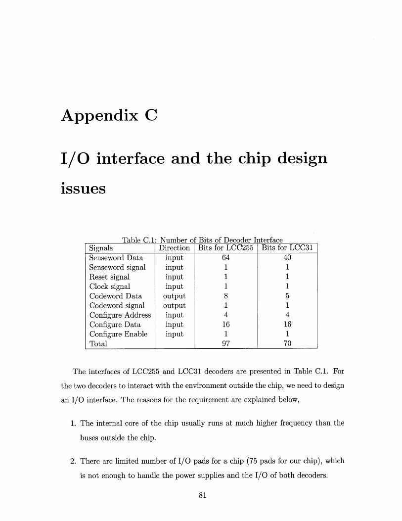
Appendix C
I/O interface and the chip design
issues
Table C.1: Number of Bits of Decoder InterfaceSignals Direction Bits for LCC255 Bits for LCC31Senseword Data input 64 40Senseword signal input 1 1Reset signal input 1 1Clock signal input 1 1Codeword Data output 8 5Codeword signal output 1 1Configure Address input 4 4Configure Data input 16 16Configure Enable input 1 1Total 97 70
The interfaces of LCC255 and LCC31 decoders are presented in Table C.1. For
the two decoders to interact with the environment outside the chip, we need to design
an I/O interface. The reasons for the requirement are explained below,
1. The internal core of the chip usually runs at much higher frequency than the
buses outside the chip.
2. There are limited number of I/O pads for a chip (75 pads for our chip), which
is not enough to handle the power supplies and the I/O of both decoders.
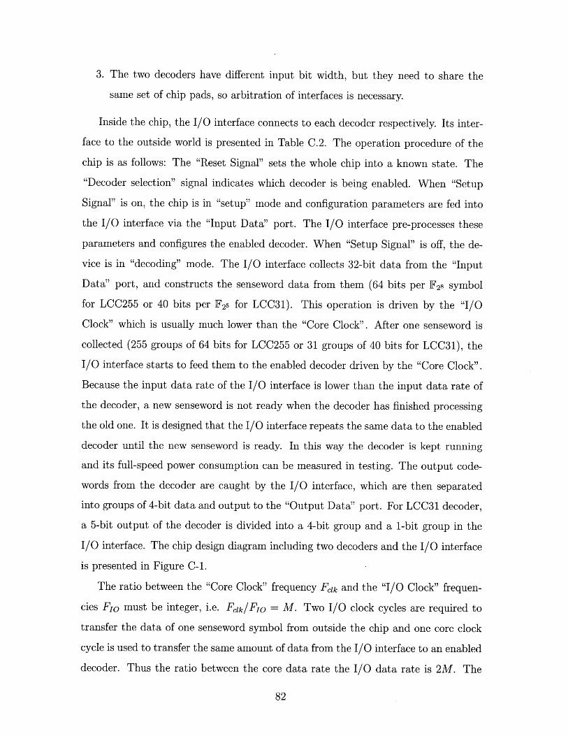
3. The two decoders have different input bit width, but they need to share the
same set of chip pads, so arbitration of interfaces is necessary.
Inside the chip, the I/O interface connects to each decoder respectively. Its inter-
face to the outside world is presented in Table C.2. The operation procedure of the
chip is as follows: The "Reset Signal" sets the whole chip into a known state. The
"Decoder selection" signal indicates which decoder is being enabled. When "Setup
Signal" is on, the chip is in "setup" mode and configuration parameters are fed into
the I/O interface via the "Input Data" port. The I/O interface pre-processes these
parameters and configures the enabled decoder. When "Setup Signal" is off, the de-
vice is in "decoding" mode. The I/O interface collects 32-bit data from the "Input
Data" port, and constructs the senseword data from them (64 bits per F 28 symbol
for LCC255 or 40 bits per F25 for LCC31). This operation is driven by the "I/O
Clock" which is usually much lower than the "Core Clock". After one senseword is
collected (255 groups of 64 bits for LCC255 or 31 groups of 40 bits for LCC31), the
I/O interface starts to feed them to the enabled decoder driven by the "Core Clock".
Because the input data rate of the I/O interface is lower than the input data rate of
the decoder, a new senseword is not ready when the decoder has finished processing
the old one. It is designed that the I/O interface repeats the same data to the enabled
decoder until the new senseword is ready. In this way the decoder is kept running
and its full-speed power consumption can be measured in testing. The output code-
words from the decoder are caught by the I/O interface, which are then separated
into groups of 4-bit data and output to the "Output Data" port. For LCC31 decoder,
a 5-bit output of the decoder is divided into a 4-bit group and a 1-bit group in the
I/O interface. The chip design diagram including two decoders and the I/O interface
is presented in Figure C-1.
The ratio between the "Core Clock" frequency Fc1k and the "I/O Clock" frequen-
cies Fro must be integer, i.e. Fek/Fro = M. Two I/O clock cycles are required to
transfer the data of one senseword symbol from outside the chip and one core clock
cycle is used to transfer the same amount of data from the I/O interface to an enabled
decoder. Thus the ratio between the core data rate the I/O data rate is 2M. The
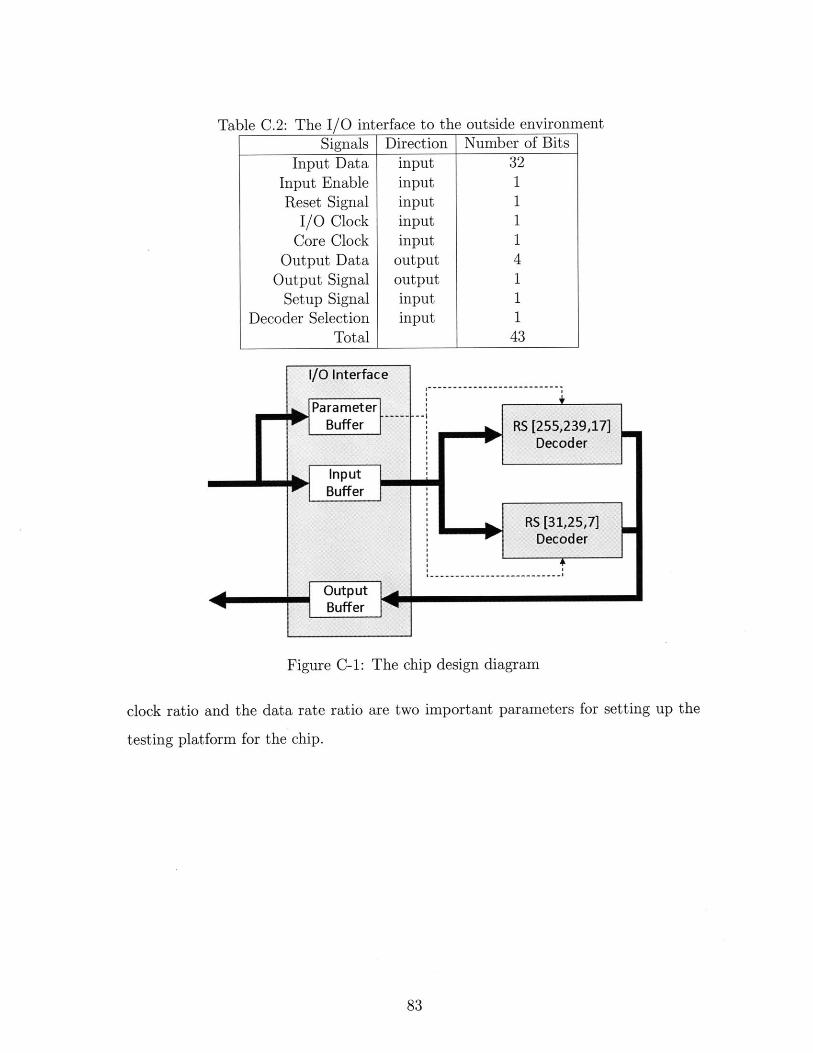
Table C.2: The I/O interface to the outside environmentSignals Direction Number of Bits
Input Data input 32Input Enable input 1Reset Signal input 1
I/O Clock input 1Core Clock input 1
Output Data output 4Output Signal output 1
Setup Signal input 1Decoder Selection input 1
Total 43
Figure C-1: The chip design diagram
clock ratio and the data rate ratio are two important parameters for setting up the
testing platform for the chip.

84

Appendix D
Physical Design and Verification
We implement our VLSI design using the standard industry-grade 90nm CMOS tech-
nology. The industry-grade standard cell libraries are also used for synthesis, place
and route. The diagram in Figure D-1 describes our ASIC design flow and the de-
sign/implementation tools used in each step. Note that the iterations between the
"Verilog Design" and "Critical Path Analysis" steps are essential in manipulating the
critical path to meet the desired running frequency.
D.1 Register file and SRAM generation
It is convenient and efficient to use generator tools to implement the storage compo-
nents, such as the relay memories in Figure 4-7 and the storage memories in Figure
4-11. There are tools for generation of register files (RF) and SRAM respectively. In
our design we use register files for small storage and SRAM for large memory blocks.
The generated storage memories are listed in Table D.1. The generator tools produce
all necessary files for synthesis, place-and-route, and verification.
D.2 Synthesis, place and route
We use Cadence RTL compiler to synthesize the Verilog design. The synthesizer
converts the RTL level design into a standard cell level design. The required input to
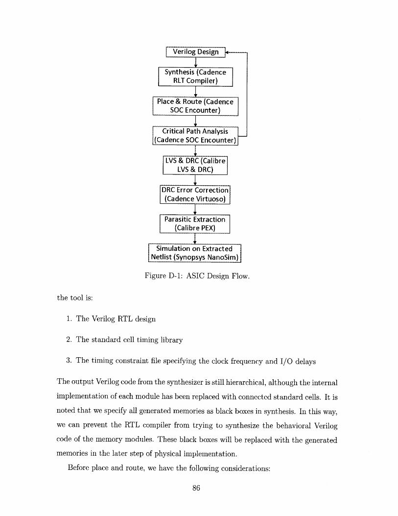
Verilog Design
Synthesis (CadenceRLT Compiler)
IPlace & Route (Cadence
SOC Encounter)
Critical Path Analysis(Cadence SOC Encounter)
LVS & DRC (CalibreLVS & DRC)
DRC Error Correction(Cadence Virtuoso)
Parasitic Extraction(Calibre PEX)
Simulation on ExtractedNetlist (Synopsys NanoSim)
Figure D-1: ASIC Design Flow.
the tool is:
1. The Verilog RTL design
2. The standard cell timing library
3. The timing constraint file specifying the clock frequency and I/O delays
The output Verilog code from the synthesizer is still hierarchical, although the internal
implementation of each module has been replaced with connected standard cells. It is
noted that we specify all generated memories as black boxes in synthesis. In this way,
we can prevent the RTL compiler from trying to synthesize the behavioral Verilog
code of the memory modules. These black boxes will be replaced with the generated
memories in the later step of physical implementation.
Before place and route, we have the following considerations:
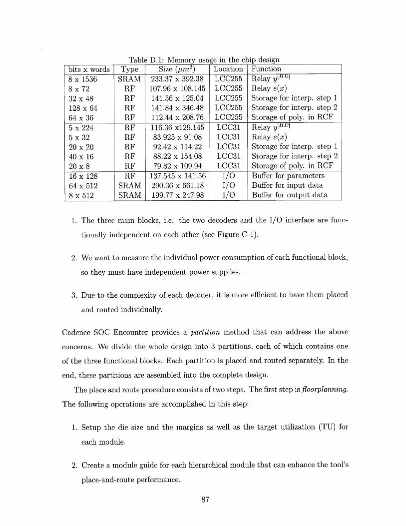
Table D.1: Memory usage in the chip design
bits x words Type Size (ym2) Location Function8 x 1536 SRAM 233.37 x 392.38 LCC255 Relay y[HDI8 x 72 RF 107.96 x 108.145 LCC255 Relay e(x)32 x 48 RF 141.56 x 125.04 LCC255 Storage for interp. step 1128 x 64 RF 141.84 x 346.48 LCC255 Storage for interp. step 264 x 36 RF 112.44 x 208.76 LCC255 Storage of poly. in RCF5 x 224 RF 116.36 x129.145 LCC31 Relay y[HD]5 x 32 RF 83.925 x 91.08 LCC31 Relay e(x)20 x 20 RF 92.42 x 114.22 LCC31 Storage for interp. step 140 x 16 RF 88.22 x 154.08 LCC31 Storage for interp. step 220 x 8 RF 79.82 x 109.94 LCC31 Storage of poly. in RCF16 x 128 RF 137.545 x 141.56 I/O Buffer for parameters64 x 512 SRAM 290.36 x 661.18 I/O Buffer for input data8 x 512 SRAM 199.77 x 247.98 I/O Buffer for output data
1. The three main blocks, i.e. the two decoders and the I/O interface are func-
tionally independent on each other (see Figure C-1).
2. We want to measure the individual power consumption of each functional block,
so they must have independent power supplies.
3. Due to the complexity of each decoder, it is more efficient to have them placed
and routed individually.
Cadence SOC Encounter provides a partition method that can address the above
concerns. We divide the whole design into 3 partitions, each of which contains one
of the three functional blocks. Each partition is placed and routed separately. In the
end, these partitions are assembled into the complete design.
The place and route procedure consists of two steps. The first step is floorplanning.
The following operations are accomplished in this step:
1. Setup the die size and the margins as well as the target utilization (TU) for
each module.
2. Create a module guide for each hierarchical module that can enhance the tool's
place-and-route performance.

3. Place hard macros such as memory blocks in appropriate positions so that the
tool can achieve better optimization results.
4. Conduct power planning and specify power rings and power grids.
The preparation work is essential for the tool to optimize its performance in the
place-and-route stage. A metric to measure the performance is the target utilization
(TU). TU is defined as the area of all standard cells and hard macros divided by the
die size. The higher value of TU is achieved, the more efficiently the design is placed
and routed. With appropriately defined module guides and correctly placed hard
macros, it is possible to achieve a TU of 80% or above. Thus, the floorplan phase of
place-and-route needs the designer's close engagement.
The floorplans of the three functional blocks are presented in Figure D-2, D-3 and
D-4 respectively. Note that the power rings and power grids are hidden for a clearer
view of the module guides and hard macro placements.
After floorplanning, the next step of place-and-route can be automated with tcl
scripts. Cadence SOC Encounter provides tools for timing analysis and power anal-
ysis in each stage of place and route. The analysis can take into consideration the
capacitance of routed wires and is thus more accurate than the analysis performed
in synthesis stage. However, the analysis is still "static" in the sense that the result
is not obtained via transient simulation. We will perform "dynamic" analysis in the
final stage of the design. Still the analysis in this stage is critical for early detection
of setup time violations and hold time violations. Moreover, by investigating the crit-
ical paths, we can easily locate the bottleneck of the clock frequency and improve the
corresponding Verilog design. Note that setup time violations can be eliminated by
lowering the clock frequency in the timing constraint. Hold time violations, however,
must be fixed by improving design. In our design, the timing analysis shows that
the circuit can run at around 250MHz without hold time violations. The running
frequency estimated at this stage is conservative. We will see that the circuit can run
at higher frequency in transient simulations.
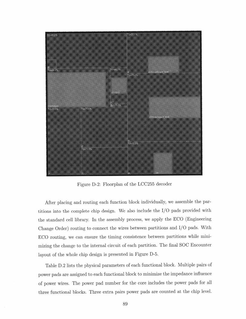
Figure D-2: Floorplan of the LCC255 decoder
After placing and routing each function block individually, we assemble the par-
titions into the complete chip design. We also include the I/O pads provided with
the standard cell library. In the assembly process, we apply the ECO (Engineering
Change Order) routing to connect the wires between partitions and I/O pads. With
ECO routing, we can ensure the timing consistence between partitions while mini-
mizing the change to the internal circuit of each partition. The final SOC Encounter
layout of the whole chip design is presented in Figure D-5.
Table D.2 lists the physical parameters of each functional block. Multiple pairs of
power pads are assigned to each functional block to minimize the impedance influence
of power wires. The power pad number for the core includes the power pads for all
three functional blocks. Three extra pairs power pads are counted at the chip level.
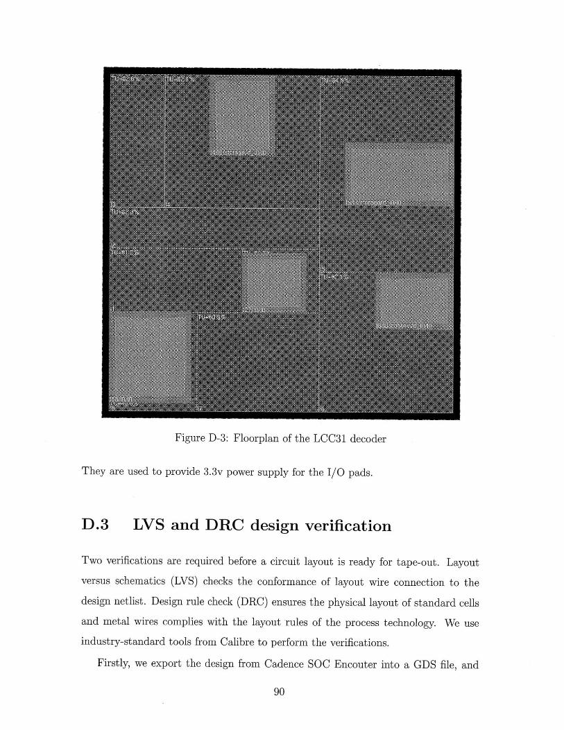
Figure D-3: Floorplan of the LCC31 decoder
They are used to provide 3.3v power supply for the I/O pads.
D.3 LVS and DRC design verification
Two verifications are required before a circuit layout is ready for tape-out. Layout
versus schematics (LVS) checks the conformance of layout wire connection to the
design netlist. Design rule check (DRC) ensures the physical layout of standard cells
and metal wires complies with the layout rules of the process technology. We use
industry-standard tools from Calibre to perform the verifications.
Firstly, we export the design from Cadence SOC Encouter into a GDS file, and
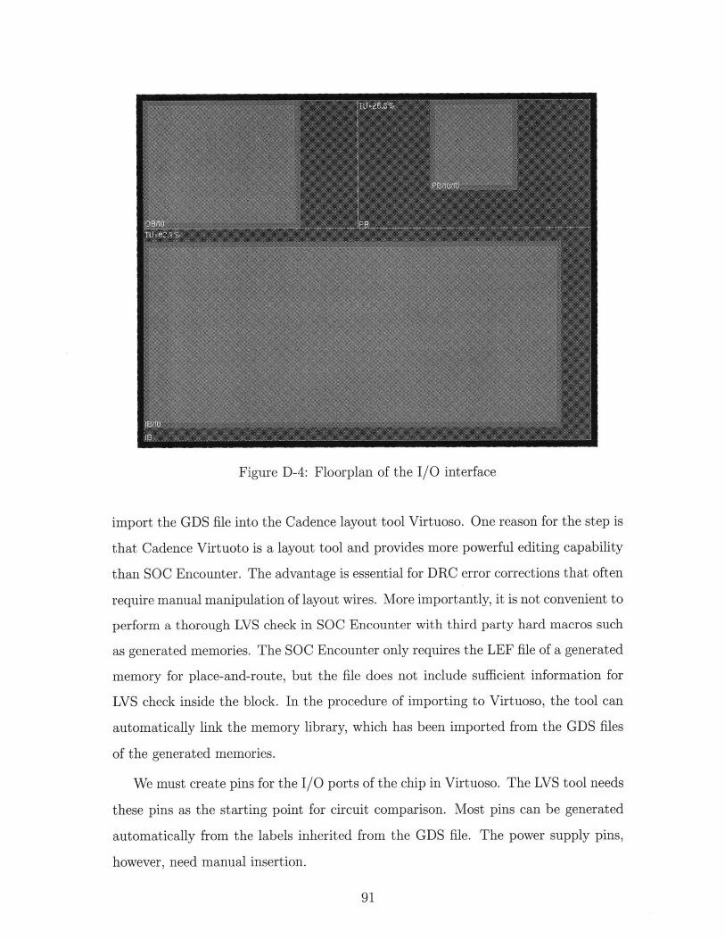
Figure D-4: Floorplan of the I/O interface
import the GDS file into the Cadence layout tool Virtuoso. One reason for the step is
that Cadence Virtuoto is a layout tool and provides more powerful editing capability
than SOC Encounter. The advantage is essential for DRC error corrections that often
require manual manipulation of layout wires. More importantly, it is not convenient to
perform a thorough LVS check in SOC Encounter with third party hard macros such
as generated memories. The SOC Encounter only requires the LEF file of a generated
memory for place-and-route, but the file does not include sufficient information for
LVS check inside the block. In the procedure of importing to Virtuoso, the tool can
automatically link the memory library, which has been imported from the GDS files
of the generated memories.
We must create pins for the I/O ports of the chip in Virtuoso. The LVS tool needs
these pins as the starting point for circuit comparison. Most pins can be generated
automatically from the labels inherited from the GDS file. The power supply pins,
however, need manual insertion.
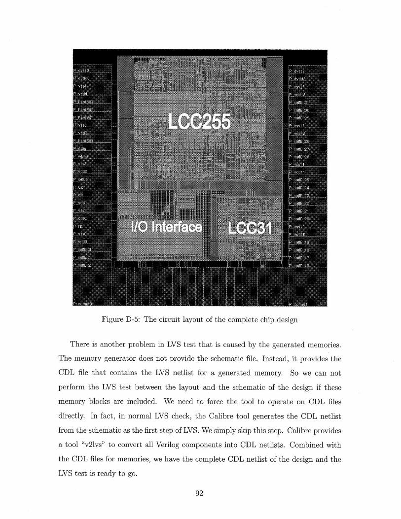
Figure D-5: The circuit layout of the complete chip design
There is another problem in LVS test that is caused by the generated memories.
The memory generator does not provide the schematic file. Instead, it provides the
CDL file that contains the LVS netlist for a generated memory. So we can not
perform the LVS test between the layout and the schematic of the design if these
memory blocks are included. We need to force the tool to operate on CDL files
directly. In fact, in normal LVS check, the Calibre tool generates the CDL netlist
from the schematic as the first step of LVS. We simply skip this step. Calibre provides
a tool "v2lvs" to convert all Verilog components into CDL netlists. Combined with
the CDL files for memories, we have the complete CDL netlist of the design and the
LVS test is ready to go.
Table D.2: Physical parameters of the circuit layoutFunctional Block Dimension (pum) Area (mm 2) Power PadsLCC255 1048.32 x 965.16 1.011 6 pairsLCC31 511 x 498.96 0.255 3 pairsI/O interface 344.96 x 347.76 0.12 4 pairsThe Core 1285.76 x 1577.52 2.028 13 pairsThe Chip 1976 x 1978 3.91 16 pairs
In DRC test the Calibre tool checks the layout wires according to the process
technology rule file. Since the place and route is mostly performed automatically by
the tools, there are usually a limited number of violations. These violations can be
easily corrected using Cadence Virtuoso layout tool.
D.4 Parasitic extraction and simulation
Table D.3: Testing cases in transient simulationsCore Clock (MHz) 250 250 333I/O Clock (MHz) 125 250 111
Transient simulation on netlists with extracted parasitics provides the most com-
prehensive verification on the final design. The power consumption measured in the
test is also the most accurate estimation. We perform the simulation on our LCC
design as the last step of verification before tape-out. We also use the measured power
consumption for design analysis.
The Calibre PEX tool is used to extract the parasitic of the circuit layout and
Synopsys Nanosim is used to perform the transient simulation. The testing vectors are
the VCD files generated from Verilog simulation. There are several viewers available
for checking the output waveforms from simulations. They all provide comparison
tools to compare the simulation result to the reference test bench.
In simulations, we verify various combinations of the I/O clock and the core clock,
as listed in Table D.3. All these cases pass the waveform comparison. Therefore, the
transient simulation indicates that the chip can run at frequency up to 333MHz,

which is higher than the frequency predicted by the timing analysis in the place and
route stage.
Bibliography
[1] A. Ahmed, R. Koetter, and N.R. Shanbhag. Vlsi architectures for soft-decisiondecoding of Reed-Solomon codes. Communications, 2004 IEEE InternationalConference on, 5(20-24):2584-2590, June 2004.
[2] J. Bellorado and A. Kavoid. A low complexity method for Chase-type decoding ofReed-Solomon codes. In Proc. IEEE International Symp. Inform. Theory (ISIT'06), pages 2037-2041, Seattle, WA, July 2006.
[3] E. Berlekamp. Nonbinary bch decoding. IEEE Transactions on InformationTheory, page 242, 1968.
[4] E. Berlekamp and L. Welch. Error correction for algebraic block codes. USPatent 4 633 470, 1986.
[5] A. P. Chandrakasan and R.W. Brodersen. Minimizing power consumption indigital cmos circuits. Proc. IEEE, 83:498-523, April 1995.
[6] D. Chase. A class of algorithms for decoding block codes with channel mea-surement information. IEEE Trans. on Inform. Theory, 18:170-182, January1972.
[7] W. J. Gross, F. Kschischang, R. Koetter, and P. G. Gulak. Towards a VLSI ar-chitecture for interpolation-based soft-decision Reed-Solomon decoders. Journalof VLSI Signal Processing Systems, 39(1/2):93-111, Jan./ Feb. 2005.
[8] W.J. Gross, F.R. Kschischang, R. Koetter, and R.G. Gulak. A vlsi architecturefor interpolation in soft-decision list decoding of reed-solomon codes. Proc. IEEEWorkshop on Signal Processing Systems, pages 39-44, Oct. 2002.
[9] V. Guruswami and M. Sudan. Improved decoding of Reed-Solomon codes andalgebraic geometry codes. IEEE Trans. on Inform. Theory, 45(6):1757-1767,September 1999.
[10] HanhoLee. A vlsi design of a high-speed reed-solomon decoder. 14th AnnualIEEE International, ASIC/SOC Conference, 12-15, pages 316-320, September2001.
[11] J. Jiang and K. R. Narayanan. Iterative soft-input soft-output decoding of Reed-Solomon codes by adapting the parity-check matrix. IEEE Trans. on Inform.Theory, 52(8):3746-3756, August 2006.
[12] J. Jiang and K. R. Narayanan. Algebraic soft-decision decoding of ReedSolomoncodes using bit-level soft information. TransIT, 54(9):3907-3928, 2008.
[13] Xinmiao Zhang Jiangli Zhu. Efficient vlsi architecture for soft-decision decodingof Reed-Solomon codes. Circuits and Systems I: Regular Papers, IEEE Trans-actions on, 55(10):3050-3062, Nov. 2008.
[14] Xinmiao Zhang Jiangli Zhu. Factorization-free low-complexity chase soft-decisiondecoding of reed-solomon codes. Circuits and Systems, IEEE International Sym-posium on, 24-27:2677-2680, May 2009.
[15] Zhongfeng Wang Jiangli Zhu, Xinmiao Zhang. Backward interpolation architec-ture for algebraic soft-decision reedcsolomon decodin. Very Large Scale Integra-tion (VLSI) Systems, IEEE Transactions on, 17(11):1602-1615, Nov. 2009.
[16] R. Koetter and A. Vardy. Algebraic soft-decision decoding of Reed-Solomoncodes. IEEE Trans. on Inform. Theory, 49(11):2809 - 2825, November 2003.
[17] R. Koetter and A. Vardy. A complexity reducing transformation in algebraiclist decoding of reed-solomon codes. Proc. Info. Theory Workshop, pages 10-13,March 2003.
[18] M-L. Yu L. Song and M. S. Shaffer. 10 and 40-gb/s forward error correc-tion devices for optical communications. IEEE Journal of Solid-State Circuits,37(11):1565-1573, November 2002.
[19] H. Lee. An area-efficient euclidean algorithm block for reed-solomon decoder.IEEE Computer Society Annual Symposium on VLSI, pages 209-210, February2003.
[20] H. Lee. High-speed vlsi architecture for parallel reed-solomon decoder. IEEETrans. On VLSI Systems, 11(2):288-294, April 2003.
[21] H. Lee. A high-speed low-complexity ReedSolomon decoder for optical commu-nications. IEEE Trans. on Circuits. and Sys., 52(8):461-465, August 2005.
[22] Hanho Lee, Meng-Lin Yu, and Leilei Song. Vlsi design of reed-solomon decoderarchitectures. IEEE International Symposium on Circuits and Systems, pages705-708, May 28-31 2000, Geneva, Switzerland.
[23] S. Lin and D. J. Costello. Error Control Coding. Pearson Prentice Hall, secondedition, 2000.
[24] Jun Ma, A. Vardy, and Zhongfeng Wang. Low-latency factorization architecturefor algebraic soft-decision decoding of Reed-Solomon codes. Very Large Scale In-tegration (VLSI) Systems, IEEE Transactions on, 15(11):1225-1238, Nov. 2007.
[25] J. Massey. -Shift register synthesis and bch decoding. IEEE Transactions onInformation Theory, pages 122-127, 1968.
[26] W. Peterson. Encoding and error-correction procedures for bose-chaudhuri codes.IRE Transactions on Information Theory, pages 459-470, 1960.
[27] G. Reed and I. Solomon. Polynomial codes over certain finite fields. Journal of
the Society for Industrial and Applied Mathematics, 8:300-304, 1960.
[28] M. Sudan. Decoding of Reed-Solomon codes beyond the error-correction bound.Journal of Complexity, 13(1):180 - 193, 1997.
[29] Y. Sugiyama, Y. Kasahara, S. Hirasawa, and T. Namekawa. A method for solvingkey equation for goppa codes. Information and Control, 27:87-89, 1975.
[30] H. Tokushige, K. Nakamaye, T. Koumoto, Y. Tang, and T. Kasami. Selectionof search centers in iterative soft-decision decoding algorithms. IEICE Trans.Fundamentals, E84-A(10):2397-2403, 2001.
[31] K.K. Xinmiao Zhang; Parhi. Implementation approaches for the advanced en-cryption standard algorithm. Circuits and Systems Magazine, IEEE, 2(4):24-46,2002.
[32] You Yu-xin, Wang Jin-xiang, Lai Feng-chang, and Ye Yi-zheng. Design andimplementation of high-speed reed-solomon decoder. ICCSC, pages 146-149,2002.
[33] Xinmiao Zhang. High-speed vlsi architecture for low-complexity chase soft-decision reed-solomon decoding. Information Theory and Applications Work-
shop, pages 422-430, Feb. 2009.