Embed Size (px)
Citation preview

Compensator Design for DC-DC Buck
Converter
using
Frequency Domain Specifications
A thesis submitted in partial fulfillment of the requirements for
the degree of
Master of Technology in
Electrical Engineering
(Specialisation: Control & Automation)
by
GAURAV KAUSHIK
Department of Electrical Engineering
National Institute of Technology, Rourkela
2014

Compensator Design for DC-DC Buck Converter
using Frequency Domain Specifications
A thesis submitted in partial fulfillment of the requirements for
the degree of
Master of Technology in
Electrical Engineering
(Specialisation: Control & Automation)
by
GAURAV KAUSHIK ROLL NO: 212EE3230
Under the Guidance of
PROF. SUSOVON SAMANTA
Department of Electrical Engineering
National Institute of Technology, Rourkela
2014
i
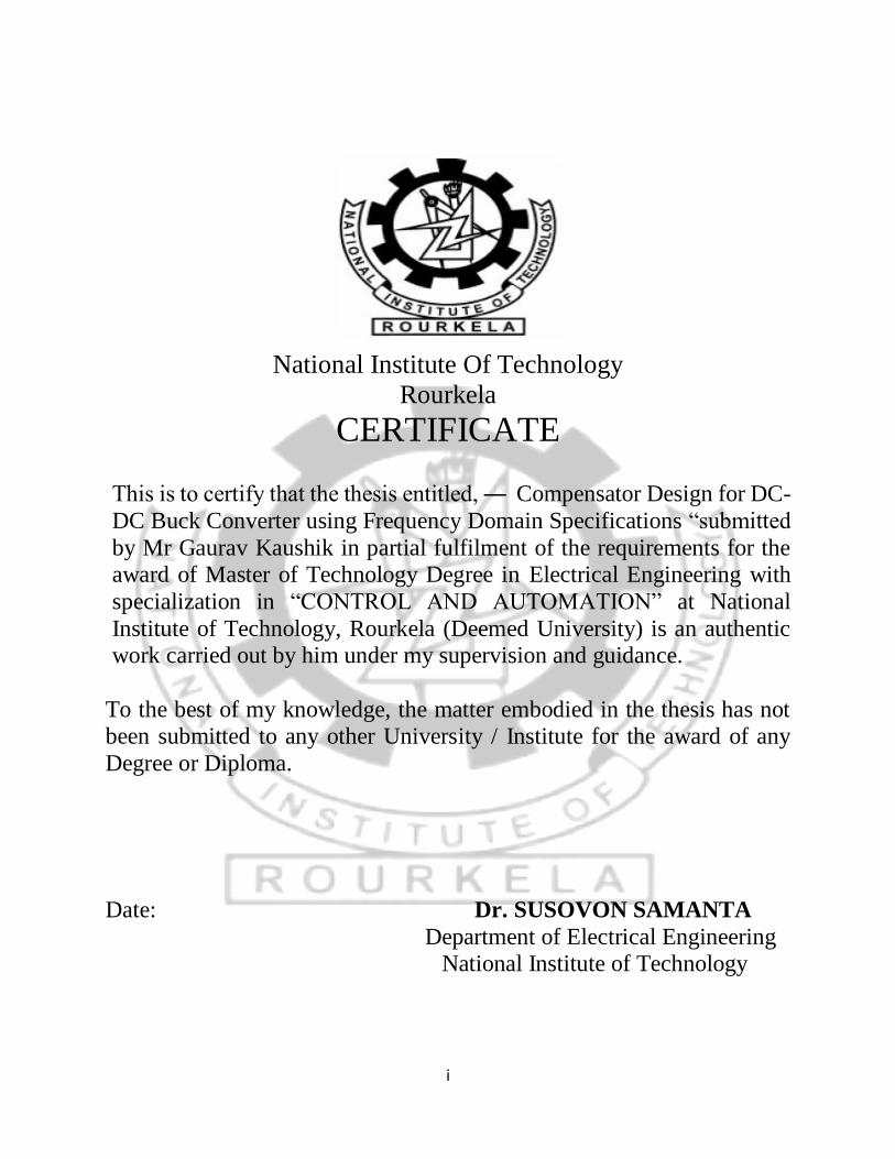
National Institute Of Technology
Rourkela
CERTIFICATE
This is to certify that the thesis entitled, ― Compensator Design for DC-
DC Buck Converter using Frequency Domain Specifications “submitted
by Mr Gaurav Kaushik in partial fulfilment of the requirements for the award of Master of Technology Degree in Electrical Engineering with
specialization in “CONTROL AND AUTOMATION” at National
Institute of Technology, Rourkela (Deemed University) is an authentic work carried out by him under my supervision and guidance.
To the best of my knowledge, the matter embodied in the thesis has not been submitted to any other University / Institute for the award of any
Degree or Diploma.
Date: Dr. SUSOVON SAMANTA
Department of Electrical Engineering National Institute of Technology

i
ACKNOWLEDGEMENTS
I am very thankful to my guide Prof. Susovon Samanta for providing me his precious knowledge
and showed trust in me during the hard time. His constant advice and efforts kept me going during
my whole research work. His deep knowledge and command over the subjects helped me to learn
a lot and had grown an insight in me. He has helped me a lot and provided me all his knowledge
to accomplish this great task.
I would also like to mention our head of department Prof.A.K. Panda to provide me with best of
the resources and facilities at NIT Rourkela. I am also thankful to Prof. Sandip Ghosh, Prof. Subojit
Ghosh, and Prof. B.D.Subudhi for their help and blessings.
Last but not the least I would also like to thank all my friends and batch mates to always encourage
and motivate me to work hard. They helped me during my hard times and helped me to face that
patiently.
Gaurav Kaushik

ii
Contents Abstract: ................................................................................................................................................................ v
Chapter 1 .............................................................................................................................................................. 1
Introduction.......................................................................................................................................................... 2
Background ........................................................................................................................................................ 2
Non Isolated Converters:................................................................................................................................. 3
Isolated Converters: ........................................................................................................................................ 3
Buck Converter: ............................................................................................................................................. 3
Boost Converter: ................................................................................................................................................ 3
Voltage Mode Control: ....................................................................................................................................... 4
Current Mode Control: ....................................................................................................................................... 5
1.2 Motivation .................................................................................................................................................... 6
1.3 Organisation of Thesis .................................................................................................................................. 6
Chapter 2 .............................................................................................................................................................. 9
Small Signal Analysis of Buck Converter ............................................................................................................ 9
2.1 Introduction .................................................................................................................................................. 9
2.2 State Space Description for Each Interval ...................................................................................................... 9
2.3 State Space Averaging ................................................................................................................................ 11
2.4 Linearization .............................................................................................................................................. 13
Chapter 3 ............................................................................................................................................................ 17
Compensator Design for DC-DC Converter ...................................................................................................... 17
3.1 Frequency-Domain Specifications ............................................................................................................... 17
3.2 Effects of Frequency Domain Specifications on the System ......................................................................... 17
3.3 Selection of compensator ............................................................................................................................ 18
3.4 Proportional controller ................................................................................................................................ 18
3.5 Proportional plus Integral (PI) ..................................................................................................................... 19
3.6 Proportional plus Derivative (PD) ............................................................................................................... 19
3.7 Proportional plus Integral plus Derivative (PID) .......................................................................................... 19
Chapter 4 ............................................................................................................................................................ 21
Compensator Tuning Methods........................................................................................................................... 21
4.1 Methods to Tune PID: ................................................................................................................................. 21
4.2 PID controller tuning using Bode’s Integral: ................................................................................................ 21
4.3 Verification of the Method: ......................................................................................................................... 23
4.3.1 Response of the System with PID: ........................................................................................................ 23
4.4 Exact Tuning of the PID Controller: ............................................................................................................ 27
4.4.1 Method to Tune: ...................................................................................................................................... 28
4.4.2 Verification of the Described Method: ...................................................................................................... 29

iii
4.5 Results From Exact Tuning Method ............................................................................................................ 29
4.6 Type III Compensator Design: .................................................................................................................... 33
4.6.1 Type-III Compensation Network .......................................................................................................... 33
4.6.2 Results From Derived Method .............................................................................................................. 34
4.7 Comparison of Result: ................................................................................................................................ 36
Frequency Domain Characteristics ................................................................................................................ 36
Step responses of system with compensators ................................................................................................. 37
4.8 Experimental Setup ..................................................................................................................................... 38
Conclusion: ......................................................................................................................................................... 39
References: ......................................................................................................................................................... 40

iv
LIST OF FIGURES:
FIGURE 1 BUCK CONVERTER ................................................................................................................................... 3 FIGURE 2 : BOOST CONVERTER ................................................................................................................................ 4 FIGURE 3: VOLTAGE MODE CONTROL ...................................................................................................................... 5 FIGURE 4: CURRENT MODE CONTROL ...................................................................................................................... 6 FIGURE 5: DURING ON TIME ....................................................................................................................................... 10 FIGURE 6: DURING OFF TIME ................................................................................................................................. 10 FIGURE 7: CLOSED LOOP MODEL OF THE SYSTEM .................................................................................................... 23 FIGURE 8: SIMULINK MODEL OF PLANT ................................................................................................................. 24 FIGURE 9: STEP RESPONSE OF SYSTEM ................................................................................................................... 24 FIGURE 10: BODE PLOT OF THE SYSTEM WITH PID ................................................................................................. 25 FIGURE 11: LOAD DISTURBANCE REJECTION OF CONTROLLER ................................................................................ 26 FIGURE 12: OUTPUT REFERENCE TRACKING........................................................................................................... 27 FIGURE 13: SIMULINK MODEL ............................................................................................................................... 30 FIGURE 14: STEP RESPONSE FOR DIFFERENT DEGREE OF FREEDOM .......................................................................... 30 FIGURE 15: BODE PLOTS OF SYSTEM WITH AND WITHOUT PID CONTROLLER........................................................... 31 FIGURE 16: LOAD DISTURBANCE REJECTION ........................................................................................................... 32 FIGURE 17: REFERENCE VOLTAGE TRACKING ........................................................................................................ 32 FIGURE 18: TYPE-III STRUCTURE ........................................................................................................................... 33 FIGURE 19: FREQUENCY RESPONSE OF THE SYSTEM WITH AND WITHOUT COMPENSATOR ........................................ 35 FIGURE 20: BODE PLOT OF THREE COMPENSATORS TOGETHER ................................................................................ 36 FIGURE 21: STEP RESPONSES OF SYSTEM WITH COMPENSATORS .............................................................................. 37 FIGURE 22: HARDWARE IMAGE.............................................................................................................................. 38 FIGURE 23: HARDWARE RESULT ............................................................................................................................ 38

v
Abstract:
In recent times integrated power management circuits have emerged as an important component
of the portable application market. Designing a power supply for meeting high efficiency and good
transient response has been a major topic for research in recent years. The DC- DC converter
demands are increasing due to their small size, high efficiency and easy to use characteristics. In
this study, we have studied few ways to design the controllers for the DC-DC converter which can
control the ripple content of the system to achieve the required performance and good regulated
voltage. The methods described can be implemented in hardware circuits very easily. The
frequency domain specifications are used to tune the controllers as they have more effect on their
performance and the calculations get simpler when working in frequency domain. These methods
gives the exact values that can be directly used unlike the earlier used trial and error procedures.
They are designed for the voltage mode controlled buck converter topology. Various controllers
like PID, TYPE-III Controller and hardware simulation is done to verify the result.

1
Chapter 1
2
Introduction
Background Dc-Dc converters are the converters that are used to convert one voltage level to another voltage
that may be higher in the magnitude or lower in the magnitude. These Dc-Dc converters are used
everywhere because of their high efficiency and single stage conversion. The control of voltage is
done by controlling the duty ratio of the switch. Switches used are Mosfets, transistors, GTO’s,
IGBT’s depending upon the circuit or the power transfer capability. Due to recent hike in the
demand of portable devices like mobiles, laptops and use of regulated power supplies in the
aerospace application, in automotive industries. In these systems the load voltage is kept constant
irrespective of the load and supply [1]. Dc-Dc converters are used extensively because in AC
system you can convert the voltage levels by the use of transformer but in DC system case is
different so these are essential for change in voltage levels in dc system. The reason for their
increased use is their cost effectiveness and simple circuitry. There is no energy generated inside
the converter, all the energy that is supplied by source is transferred to load with little losses, to
different voltage and current level. The applications where they are used day to day is running of
CD player, to supply the motherboard of personal computers. They are also used in the satellites
where dc buses at different voltage levels are supplied through these dc-dc converters.
They are of two kinds:
1. Non Isolated Converters
2. Isolated Converters

3
Non Isolated Converters: In these type of converters the voltage level step-up or step-down ratio is not that much high to
create a problem and can be used without isolation. [2]The topologies that are generally used for
this category are buck, boost, buck-boost and Cuk. They share common connection.
Isolated Converters: In these type of converters the voltage level step-up or step down ratio is very high so that use of
electrical isolation is indispensable. Here output side is completely isolated from the source side.
This ensures the safe operation of converter. There are two topologies that are used largely in this
category are flyback converter and forward converter. For us the concern is the non-isolated dc-dc
converter.
Buck Converter: In this converter the output is connected to the source during the time switch is on and when switch
is off output is supplied through the capacitor and inductor via freewheeling diode [2]. In this way
the output current is continuous and load voltage switches between the Vin and zero. The average
load voltage is less than the supplied input voltage.
Boost Converter: [2]In this converter the output voltage is more than the supply voltage. When switch is on source
charges the inductor and inductor stores energy, when switch is off the load is supplied by source
Figure 1 Buck Converter
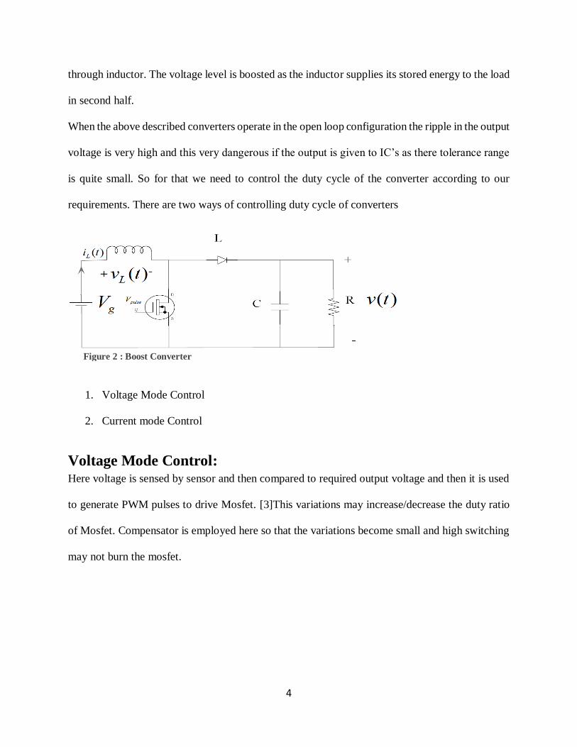
4
through inductor. The voltage level is boosted as the inductor supplies its stored energy to the load
in second half.
When the above described converters operate in the open loop configuration the ripple in the output
voltage is very high and this very dangerous if the output is given to IC’s as there tolerance range
is quite small. So for that we need to control the duty cycle of the converter according to our
requirements. There are two ways of controlling duty cycle of converters
1. Voltage Mode Control
2. Current mode Control
Voltage Mode Control: Here voltage is sensed by sensor and then compared to required output voltage and then it is used
to generate PWM pulses to drive Mosfet. [3]This variations may increase/decrease the duty ratio
of Mosfet. Compensator is employed here so that the variations become small and high switching
may not burn the mosfet.
Figure 2 : Boost Converter

5
Current Mode Control: In this mode the current input to inductor is sensed by the sensor and then it is compared with the
controllers output and fed to the SR flip flop so that the pulses [4]can be generated to drive the
Mosfet. It has two loops one inner current loop that controls the inductor current and outer voltage
loop that controls output voltage which in turn is controlled by the inner loop.
But it has some advantage over the voltage mode control:
Current through the switch is limited to its maximum value so that the switch do not get burnt
or damaged.
Protection during overload.
Operating the converters in parallel is easy with this control.
Figure 3: Voltage Mode Control

6
1.2 Motivation:
As the need of the portable devices are increasing day by day and the need for cheap and efficient
regulated power supplies are increasing simultaneously. The need for controlled ripple regulated
supply makes it indispensable to search for the compensator design such that closed loop control
of the voltage make the ripple in the range of 1-2% of supply voltage.
1.3 Organisation of Thesis:
This thesis work is divided into five chapters. Chapter 1 gives a brief introduction about the DC-
DC converters and their background. This tell us what the different types of configuration are and
Figure 4: Current Mode Control

7
the how one is different from another and what their individual advantages are. Chapter 2 describes
how we model the buck regulator and derive the transfer function to be used for designing the
compensator. The small signal analysis is done to see the variation of the converter characteristics
around the desired point of operation. Chapter 3 covers how to select the compensator and make
correct choice while there is confusion between any compensators. Various compensators are
shown and there effects on the system are described so as to ease the process of selection. Chapter
4 describes few methods taken from literature to design the PID controller, Type-II compensator,
Type III compensator and their frequency responses are shown. The hardware design and their
responses are also shown. Chapter 5 describes the conclusions drawn from the work done and
suggested future work that can be done in this area.

8
Chapter 2
9
Chapter 2
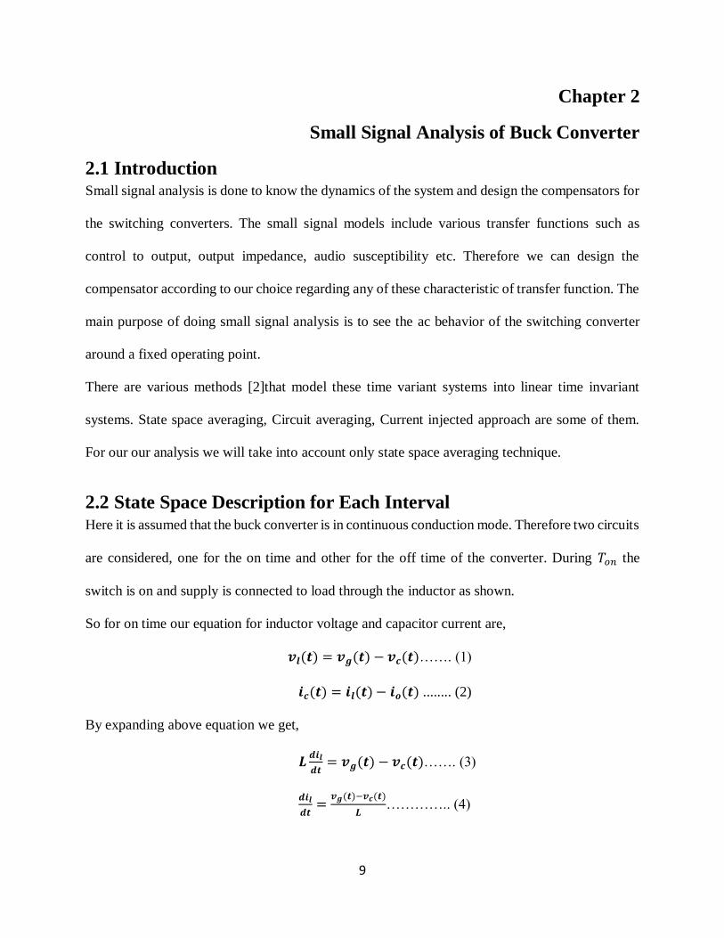
Small Signal Analysis of Buck Converter
2.1 Introduction Small signal analysis is done to know the dynamics of the system and design the compensators for
the switching converters. The small signal models include various transfer functions such as
control to output, output impedance, audio susceptibility etc. Therefore we can design the
compensator according to our choice regarding any of these characteristic of transfer function. The
main purpose of doing small signal analysis is to see the ac behavior of the switching converter
around a fixed operating point.
There are various methods [2]that model these time variant systems into linear time invariant
systems. State space averaging, Circuit averaging, Current injected approach are some of them.
For our our analysis we will take into account only state space averaging technique.
2.2 State Space Description for Each Interval Here it is assumed that the buck converter is in continuous conduction mode. Therefore two circuits
are considered, one for the on time and other for the off time of the converter. During 𝑇𝑜𝑛 the
switch is on and supply is connected to load through the inductor as shown.
So for on time our equation for inductor voltage and capacitor current are,
𝒗𝒍(𝒕) = 𝒗𝒈(𝒕) − 𝒗𝒄(𝒕)……. (1)
𝒊𝒄(𝒕) = 𝒊𝒍(𝒕) − 𝒊𝒐(𝒕) ........ (2)
By expanding above equation we get,
𝑳𝒅𝒊𝒍
𝒅𝒕= 𝒗𝒈(𝒕) − 𝒗𝒄(𝒕)……. (3)
𝒅𝒊𝒍
𝒅𝒕=
𝒗𝒈(𝒕)−𝒗𝒄(𝒕)
𝑳………….. (4)

10
Similarly for the capacitor current,
𝑪𝒅𝒗𝒄
𝒅𝒕= 𝒊𝒍(𝒕) − 𝒊𝒐(𝒕)….. (5)
𝒅𝒗𝒄
𝒅𝒕=
𝒊𝒍(𝒕)
𝑪−
𝒗𝒄(𝒕)
𝑹𝑪……… (6)
Now the above equations can be written as,
[
𝑑𝑖𝑙
𝑑𝑡𝑑𝑣𝑐
𝑑𝑡
] = [0 −1/𝐿
−1/𝐶 −1/𝑅𝐶] [
𝑖𝑙
𝑣𝑐] + [
−1/𝐿0
] [𝑣𝑔]
𝑦 = [0 1] [𝑖𝑙
𝑣𝑐]
They may be written as,
�̇� = 𝐴𝑜𝑛𝑥 + 𝐵𝑜𝑛𝑢
𝑦 = 𝐶𝑜𝑛𝑥 + 𝐷𝑜𝑛𝑢
Here, 𝐷𝑜𝑛=0
Now we analyze the off time circuit,
During off time the switch is open and the load current is supplied by the inductor stored energy.
And this path is completed through the diode.
During this time inductor voltage is,
𝒗𝒍(𝒕) = −𝒗𝒄(𝒕)
𝒅𝒊𝒍
𝒅𝒕= −
𝒗𝒄(𝒕)
𝑳
Similarly for capacitor current,
𝑖𝑐(𝑡) = 𝑖𝑙(𝑡) − 𝑖𝑜(𝑡)
𝑑𝑣𝑐
𝑑𝑡=
𝑖𝑙(𝑡)
𝐶−
𝑣𝑐(𝑡)
𝑅𝐶
These can also be written as,
Figure 5: During On Time
Figure 6: During Off Time

11
[
𝑑𝑖𝑙
𝑑𝑡𝑑𝑣𝑐
𝑑𝑡
] = [0 −1
−1/𝐶 −1/𝑅𝐶] [
𝑖𝑙(𝑡)𝑣𝑐(𝑡)
] + [00
] [𝑣𝑔]
𝑦 = [0 1] [𝑖𝑙(𝑡)𝑣𝑐(𝑡)
]
Above equations can be rewritten as,
�̇� = 𝐴𝑜𝑓𝑓𝑥 + 𝐵𝑜𝑓𝑓𝑢
𝑦 = 𝐶𝑜𝑓𝑓𝑥 + 𝐷𝑜𝑓𝑓𝑢
Here 𝐷𝑜𝑓𝑓 = 0
From above equations we can see that 𝐴𝑜𝑛 = 𝐴𝑜𝑓𝑓 and 𝐵𝑜𝑓𝑓 = 0
2.3 State Space Averaging
Let the converter switch be on for the time 𝑑𝑛𝑇 i.e. 𝑡𝑜𝑛 and 𝑑𝑛′ 𝑇 is the interval for which
switch is off i.e. 𝑡𝑜𝑓𝑓 = 𝑑𝑛′ 𝑇 = (1 − 𝑑𝑛)𝑇 .
The state space description can be written as
ON: �̇�(𝑡) = 𝐴𝑜𝑛𝑥(𝑡) + 𝐵𝑜𝑛𝑢(𝑡) for time 𝑡 ∈ [𝑛𝑇, 𝑛𝑇 + 𝑑𝑛𝑇], n=1, 2, 3… (1)
OFF:�̇�(𝑡) = 𝐴𝑜𝑓𝑓𝑥(𝑡) + 𝐵𝑜𝑓𝑓𝑢(𝑡) for time 𝑡 ∈ [𝑛𝑇 + 𝑑𝑛𝑇, (𝑛 + 1)𝑇 ] n=1, 2, 3… (2)
The solutions to the above equations can be found by taking the integration over each interval
of operation,
𝑥(𝑛 + 𝑑𝑛)𝑇 = 𝑒𝐴𝑜𝑛𝑑𝑛𝑡𝑥(𝑛𝑇) + 𝐴𝑜𝑛−1(𝑒𝐴𝑜𝑛𝑑𝑛𝑡 − 𝐼)𝐵𝑜𝑛𝑢 (3)
𝑥(𝑛 + 1)𝑇 = 𝑒𝐴𝑜𝑓𝑓𝑑𝑛′ 𝑇𝑥(𝑛𝑇 + 𝑑𝑛𝑇) + 𝐴𝑜𝑓𝑓
−1 (𝑒𝐴𝑜𝑓𝑓𝑑𝑛′ 𝑇 − 𝐼)𝐵𝑜𝑓𝑓𝑢 (4)
Substituting (3) in (4)
𝑥(𝑛 + 1)𝑇 = (𝑒𝐴𝑜𝑓𝑓𝑑𝑛′ 𝑇(𝑒𝐴𝑜𝑛𝑑𝑛𝑡𝑥(𝑛𝑇) + 𝐴𝑜𝑛
−1(𝑒𝐴𝑜𝑛𝑑𝑛𝑡 − 𝐼)𝐵𝑜𝑛𝑢)) + 𝐴𝑜𝑓𝑓−1 (𝑒𝐴𝑜𝑓𝑓𝑑𝑛
′ 𝑇 − 𝐼)𝐵𝑜𝑓𝑓𝑢
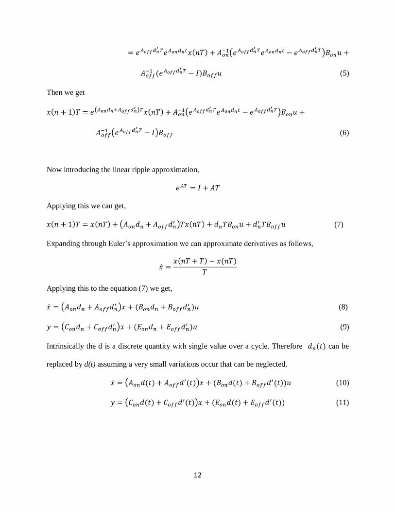
12
= 𝑒𝐴𝑜𝑓𝑓𝑑𝑛′ 𝑇𝑒𝐴𝑜𝑛𝑑𝑛𝑡𝑥(𝑛𝑇) + 𝐴𝑜𝑛
−1(𝑒𝐴𝑜𝑓𝑓𝑑𝑛′ 𝑇𝑒𝐴𝑜𝑛𝑑𝑛𝑡 − 𝑒𝐴𝑜𝑓𝑓𝑑𝑛
′ 𝑇)𝐵𝑜𝑛𝑢 +
𝐴𝑜𝑓𝑓−1 (𝑒𝐴𝑜𝑓𝑓𝑑𝑛
′ 𝑇 − 𝐼)𝐵𝑜𝑓𝑓𝑢 (5)
Then we get
𝑥(𝑛 + 1)𝑇 = 𝑒(𝐴0𝑛𝑑𝑛+𝐴𝑜𝑓𝑓𝑑𝑛′ )𝑇𝑥(𝑛𝑇) + 𝐴𝑜𝑛
−1(𝑒𝐴𝑜𝑓𝑓𝑑𝑛′ 𝑇𝑒𝐴𝑜𝑛𝑑𝑛𝑡 − 𝑒𝐴𝑜𝑓𝑓𝑑𝑛
′ 𝑇)𝐵𝑜𝑛𝑢 +
𝐴𝑜𝑓𝑓−1 (𝑒𝐴𝑜𝑓𝑓𝑑𝑛
′ 𝑇 − 𝐼)𝐵𝑜𝑓𝑓 (6)
Now introducing the linear ripple approximation,
𝑒𝐴𝑇 = 𝐼 + 𝐴𝑇
Applying this we can get,
𝑥(𝑛 + 1)𝑇 = 𝑥(𝑛𝑇) + (𝐴𝑜𝑛𝑑𝑛 + 𝐴𝑜𝑓𝑓𝑑𝑛′ )𝑇𝑥(𝑛𝑇) + 𝑑𝑛𝑇𝐵𝑜𝑛𝑢 + 𝑑𝑛
′ 𝑇𝐵𝑜𝑓𝑓𝑢 (7)
Expanding through Euler’s approximation we can approximate derivatives as follows,
�̇� =𝑥(𝑛𝑇 + 𝑇) − 𝑥(𝑛𝑇)
𝑇
Applying this to the equation (7) we get,
�̇� = (𝐴𝑜𝑛𝑑𝑛 + 𝐴𝑜𝑓𝑓𝑑𝑛′ )𝑥 + (𝐵𝑜𝑛𝑑𝑛 + 𝐵𝑜𝑓𝑓𝑑𝑛
′ )𝑢 (8)
𝑦 = (𝐶𝑜𝑛𝑑𝑛 + 𝐶𝑜𝑓𝑓𝑑𝑛′ )𝑥 + (𝐸𝑜𝑛𝑑𝑛 + 𝐸𝑜𝑓𝑓𝑑𝑛
′ )𝑢 (9)
Intrinsically the d is a discrete quantity with single value over a cycle. Therefore 𝑑𝑛(𝑡) can be
replaced by d(t) assuming a very small variations occur that can be neglected.
�̇� = (𝐴𝑜𝑛𝑑(𝑡) + 𝐴𝑜𝑓𝑓𝑑′(𝑡))𝑥 + (𝐵𝑜𝑛𝑑(𝑡) + 𝐵𝑜𝑓𝑓𝑑′(𝑡))𝑢 (10)
𝑦 = (𝐶𝑜𝑛𝑑(𝑡) + 𝐶𝑜𝑓𝑓𝑑′(𝑡))𝑥 + (𝐸𝑜𝑛𝑑(𝑡) + 𝐸𝑜𝑓𝑓𝑑′(𝑡)) (11)
13
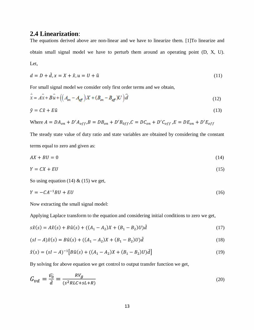
2.4 Linearization: The equations derived above are non-linear and we have to linearize them. [1]To linearize and
obtain small signal model we have to perturb them around an operating point (D, X, U).
Let,
𝑑 = 𝐷 + �̂�, 𝑥 = 𝑋 + �̂�, 𝑢 = 𝑈 + �̂� (11)
For small signal model we consider only first order terms and we obtain,
(12)
�̂� = 𝐶�̂� + 𝐸�̂� (13)
Where 𝐴 = 𝐷𝐴𝑜𝑛 + 𝐷′𝐴𝑜𝑓𝑓,𝐵 = 𝐷𝐵𝑜𝑛 + 𝐷′𝐵0𝑓𝑓 ,𝐶 = 𝐷𝐶𝑜𝑛 + 𝐷′𝐶𝑜𝑓𝑓 ,𝐸 = 𝐷𝐸𝑜𝑛 + 𝐷′𝐸𝑜𝑓𝑓
The steady state value of duty ratio and state variables are obtained by considering the constant
terms equal to zero and given as:
𝐴𝑋 + 𝐵𝑈 = 0 (14)
𝑌 = 𝐶𝑋 + 𝐸𝑈 (15)
So using equation (14) & (15) we get,
𝑌 = −𝐶𝐴−1𝐵𝑈 + 𝐸𝑈 (16)
Now extracting the small signal model:
Applying Laplace transform to the equation and considering initial conditions to zero we get,
𝑠�̂�(𝑠) = 𝐴�̂�(𝑠) + 𝐵�̂�(𝑠) + ((𝐴1 − 𝐴2)𝑋 + (𝐵1 − 𝐵2)𝑈)�̂� (17)
(𝑠𝐼 − 𝐴)�̂�(𝑠) = 𝐵�̂�(𝑠) + ((𝐴1 − 𝐴2)𝑋 + (𝐵1 − 𝐵2)𝑈)�̂� (18)
�̂�(𝑠) = (𝑠𝐼 − 𝐴)−1[𝐵�̂�(𝑠) + ((𝐴1 − 𝐴2)𝑋 + (𝐵1 − 𝐵2)𝑈)�̂�] (19)
By solving for above equation we get control to output transfer function we get,
𝐺𝑣𝑑 =𝑣0̂
�̂�=
𝑅𝑉𝑔
(𝑠2𝑅𝐿𝐶+𝑠𝐿+𝑅) (20)
14
If all the non-ideal case is considered, then during on time the converter circuit will be like this.
The corresponding state space equation,
[𝑖�̇�
𝑣�̇�] = [
−1
𝐿(𝑟𝐿 + 𝑟𝑑𝑠𝑜𝑛 +
𝑅𝑟𝑐
𝑅+𝑟𝑐−
1
𝐿
𝑅
(𝑅+𝑟𝑐)
𝑅
𝐶(𝑅+𝑟𝑐)−
1
𝐶(𝑅+𝑟𝑐)
] [𝑖𝐿
𝑣𝑐] + [
1
𝐿−
𝑟𝑐𝑅
𝐿(𝑅+𝑟𝑐)0
0𝑅
𝐶(𝑅+𝑟𝑐)0
] [
𝑣𝑔
𝑖𝑙𝑜𝑎𝑑
𝑣𝑑
] (21)
[𝑣0
𝑖𝐿] = [
𝑅𝑟𝑐
𝑅+𝑟𝑐
𝑅
𝑅+𝑟𝑐
1 0] [
𝑖𝐿
𝑣𝑐] + [
0𝑟𝑐𝑅
𝑅+𝑟𝑐0
0 0 0] [
𝑣𝑔
𝑖𝑙𝑜𝑎𝑑
𝑣𝑑
] (22)
When the switch is off the circuit of converter shown below
[𝑖�̇�
𝑣�̇�] = [
−1
𝐿(𝑟𝐿 + 𝑟𝑑 +
𝑅𝑟𝑐
𝑅+𝑟𝑐−
1
𝐿
𝑅
(𝑅+𝑟𝑐)
𝑅
𝐶(𝑅+𝑟𝑐)
1
𝐶(𝑅+𝑟𝑐)
] [𝑖𝐿
𝑣𝑐] + [
0 −𝑟𝑐𝑅
𝐿(𝑅+𝑟𝑐)−
1
𝐿
0𝑅
𝐶(𝑅+𝑟𝑐)0
] [
𝑣𝑔
𝑖𝑙𝑜𝑎𝑑
𝑣𝑑
] (23)
[𝑣0
𝑖𝐿] = [
𝑅𝑟𝑐
𝑅+𝑟𝑐
𝑅
𝑅+𝑟𝑐
1 0] [
𝑖𝐿
𝑣𝑐] + [
0𝑟𝑐𝑅
𝑅+𝑟𝑐0
0 0 0] [
𝑣𝑔
𝑖𝑙𝑜𝑎𝑑
𝑣𝑑
] (24)
By using state space averaging as done in above ideal case and after linearizing the equation it
can be write that,
𝑉0 =𝑅𝑟𝑐
𝑅+𝑟𝑐𝐼𝐿 +
𝑅
𝑅+𝑟𝑐𝑉𝑐 (25)
Where, 𝐼𝐿 =𝐷𝑝𝑉𝑔
𝑎−
(1−𝐷𝑝)𝑉𝑑
𝑎 and 𝑉𝑐 =
𝑅𝐷𝑝𝑉𝑔
𝑎−
𝑅(1−𝐷𝑝)𝑉𝑑
𝑎 (26)
By putting the value of 𝐼𝐿 and 𝑉𝑐 in equation no. (5)
𝑉0 =𝑅𝑟𝑐
𝑅+𝑟𝑐×
𝐷𝑝𝑉𝑔
𝑎−
𝑅𝑟𝑐
𝑅+𝑟𝑐×
(1−𝐷𝑝)𝑉𝑑
𝑎+
𝑅
𝑅+𝑟𝑐×
𝑅𝐷𝑝𝑉𝑔
𝑎−
𝑅
𝑅+𝑟𝑐×
𝑅(1−𝐷𝑝)𝑉𝑑
𝑎 (27)

15
Now, 𝑟𝑜𝑛 = 𝑟𝐿 + 𝑟𝑑𝑠𝑜𝑛 , 𝑟𝑜𝑓𝑓 = 𝑟𝐿 + 𝑟𝑑 and 𝑎 = 𝑅 + 𝐷𝑃𝑟𝑜𝑛 + 𝐷𝑃𝑟𝑜𝑓𝑓
So, for a given output voltage and input voltage the duty ratio with parasitic is derived as,
𝐷𝑝 =𝑉0(𝑅+𝑟𝑜𝑓𝑓)+𝑉𝑑𝑅
𝑉0(𝑟𝑜𝑓𝑓−𝑟𝑜𝑛)+𝑅(𝑉𝑔+𝑉𝑑) (28)
After obtaining steady state values of 𝐷𝑃 , 𝐼𝐿 and 𝑉𝑐 , all the transfer function arising out of the
state space model can be derived for open loop power stage. Assume that the state of the
incremental linearizing model is zero initially.
Then the transfer function is,
𝐺𝑣𝑑(𝑠) =𝑅(𝑉𝑔+𝑉𝑑+𝐼𝐿(𝑟𝑜𝑓𝑓−𝑟𝑜𝑛)(1+𝑠𝐶𝑟𝑐
∆(𝑠) (29)
Where,
∆(𝑠) = 𝑠2𝐿𝐶(𝑅 + 𝑟𝑐) + 𝑠[𝐿 + 𝑅𝐶{(𝑟𝑐 + 𝑟𝑜𝑓𝑓) + 𝐷𝑝(𝑟𝑜𝑛 − 𝑟𝑜𝑓𝑓)} + 𝑟𝑐𝐶{𝐷𝑝(𝑟𝑜𝑛 − 𝑟𝑜𝑓𝑓) +
𝑟𝑜𝑓𝑓}] + 𝑅 + 𝐷𝑝𝑟𝑜𝑛 + 𝐷𝑝𝑟𝑜𝑓𝑓 (30)

16
Chapter 3

17
Chapter 3
Compensator Design for DC-DC Converter Fixed structure compensators are those compensators whose design remain fixed for a particular
DC-DC converter and for a change in plant only values of the resistance and capacitance values
need to be changed. There are many ways to design these compensators based on the time-domain
and frequency-domain specification as these characteristics define the characteristics of the
system. Here we will show how to design the compensator based on the frequency-domain
specification.
3.1 Frequency-Domain Specifications [5]:
1. Gain Margin: it is the amount of change required in open loop gain to make the system
unstable.
2. Phase Margin: it is the amount of change required in open loop phase shift to make a closed
loop system unstable.
3. Bandwidth: the bandwidth is frequency at which the closed loop systems gain falls to -3db.
4. Nyquist Slope: its new and effective method to shape the loop characteristics.
3.2 Effects of Frequency Domain Specifications on the System:
1. Gain Margin: increasing gain margin helps us to remove low frequency noise problems
and increase in dc gain also makes system a little faster.
2. Phase margin: low phase margin causes closed loop system to exhibit overshoot and
ringing. It is closely related to closed loop damping factor.

18
3. Bandwidth: it helps to remove the sensor noise used to sense the current/voltage in the
closed loop system. It also affect the rise time of the system.
4. Nyquist slope: it helps to shape the loop so that the slope of magnitude curve is -
20db/decade at crossover frequency and the phase curve gives phase margin of the -90 so
that robust controllers may be designed.
3.3 Selection of compensator [3]:
There are four compensators among which we have to choose P, PI, PD and PID. The selection is
based on the following characteristics:
a. Rise Time
b. Maximum Overshoot
c. Steady State Error
d. Settling Time
We have to select what suits best to our requirement.
3.4 Proportional controller:
It is mainly used to reduce the steady state error and as the gain of proportional controller is
increased the steady state error starts to decrease with decrease in rise time. But despite the
reduction in the steady state error it can never completely eliminate the error. Also it increases the
maximum overshoot of the system. It makes the dynamics of the system faster with larger
bandwidth but also makes system more susceptible to noise. Large value of K (proportional gain)
can also make system unstable.

19
3.5 Proportional plus Integral (PI):
Integral term is mainly used to eliminate the steady state error but at the cost of the reduced speed
of the system. Proportional term used is used to compensate the lag produced by integral term but
overall system lags its earlier speed. Also it can boost the oscillations and maximum overshoot.
3.6 Proportional plus Derivative (PD):
It is mainly used to boost the dynamics of the system and increase the stability of the system. The
derivative control is not used alone because of the problem of amplifying the noise.it has very less
effect on the steady state error of the system.
3.7 Proportional plus Integral plus Derivative (PID):
PID has fast dynamics, zero steady state error and no oscillations with high stability. It has the
advantage is that it can be applied to system of any order. Derivative gain in addition to PI is to
increase the speed of response and decrease overshoot and oscillations. There are lots of tuning
methods available including online tuning including iterative procedures, offline tuning using the
pen and pencil. According to the advantages offered by PID over other we select PID and here we
present two methods to tune the parameters of PID.

20
Chapter 4

21
Chapter 4
Compensator Tuning Methods
4.1 Methods to Tune PID: Two methods are as follows:
1) PID controller tuning using Bode’s Integral
2) Exact tuning of PID controller based on the PM, Bandwidth and GM
4.2 PID controller tuning using Bode’s Integral:
Motivation:
This method to tune is selected because this method can give the vales of controller parameters in
single step and we don’t have to go for the iterative method and also this method provides with the
equation that can be with pen and paper instead of going for any software [3].
This method uses the two new relations derived from Bode’s integral i.e. derivative of amplitudes
relation to phase of the system and the derivative of phase relation to amplitude of the system at
the crossover frequency. Also it uses one term called the Nyquist slope of the curve that will be
used to shape the loop response around the crossover frequency. These two relations are as follows:
…. (1)
….. (2)
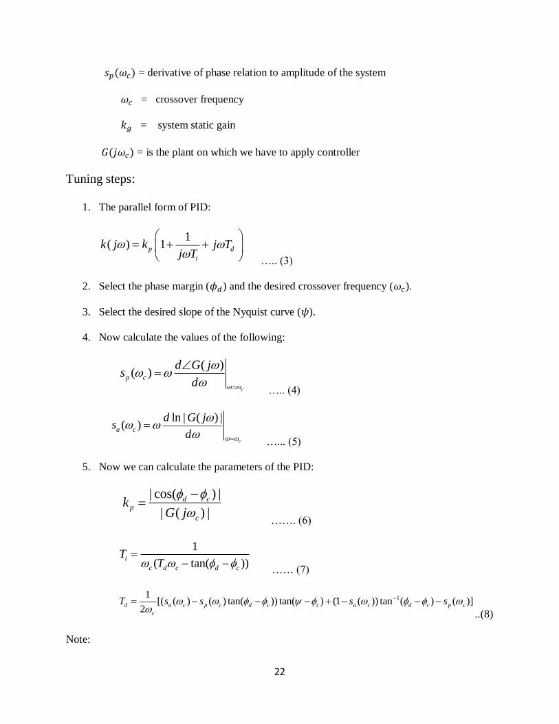
Where 𝑠𝑎(𝜔𝑐) = derivative of amplitudes relation to phase of the system
ln | ( ) | 2( ) ( )c
a c c c
d G js G j
d
2( ) ( ) ln | | ln | ( ) |p c c g cs G j k G j
22
𝑠𝑝(𝜔𝑐) = derivative of phase relation to amplitude of the system
𝜔𝑐 = crossover frequency
𝑘𝑔 = system static gain
𝐺(𝑗𝜔𝑐) = is the plant on which we have to apply controller
Tuning steps:
1. The parallel form of PID:
….. (3)
2. Select the phase margin (𝜙𝑑) and the desired crossover frequency (𝜔𝑐).
3. Select the desired slope of the Nyquist curve (𝜓).
4. Now calculate the values of the following:
….. (4)
…... (5)
5. Now we can calculate the parameters of the PID:
……. (6)
…… (7)
..(8)
Note:
1( ) 1p d
i
k j k j Tj T
( )( )
c
p c
d G js
d
ln | ( ) |( )
c
a c
d G js
d
| cos( ) |
| ( ) |
d cp
c
kG j
1
( tan( ))i
c d c d c
TT
11[( ( ) ( ) tan( )) tan( ) (1 ( )) tan ( ) ( )]
2d a c p c d c c a c d c p c
c
T s s s s

23
If the plant has pole at origin then the systems static gain is calculated without that pole and then
applied to equation(2) to get the value of derivative of phase.
4.3 Verification of the Method:
The above is applied to the buck converter to verify whether the parameter values obtained from
the previous method gives the satisfactory result or not.
Parameter values of the Buck converter:
Inductor (L) =50µH, Output Capacitor(C) =500µF, R=3𝛺, Switching Frequency=100 kHz
Input voltage=28V, Output voltage=15V, Output current=3A
For the above specifications, the control to output transfer function is as follows,
We choose ∅𝑑=520 ,𝑓𝑐 = 5𝑘𝐻𝑧 and ψ=350, and we get controller parameters as follows,
4.3.1 Response of the System with PID:
Closed loop model of the system:
0
2 8 6
2.33( )
2.58 10 16.67 10 1
vG s
s sd
3 66.42, 1.35 10 , 40 10p i dk T T
Figure 7: Closed loop model of the system

24
Simulink Model of Plant:
Step Response of System:
Figure 8: Simulink Model of Plant
Figure 9: Step Response of System

25
Bode Plot of the System with PID:
Inference from plot:
The dc gain of the system with PID is very large as compared to the original system. This
helps to remove the low frequency noise and also improves the rise time of the system.
We can also see that the bandwidth is also increased which is done intentionally to improve
the systems immunity against sensor noise and against the high frequency noise.
Figure 10: Bode Plot of the System with PID
26
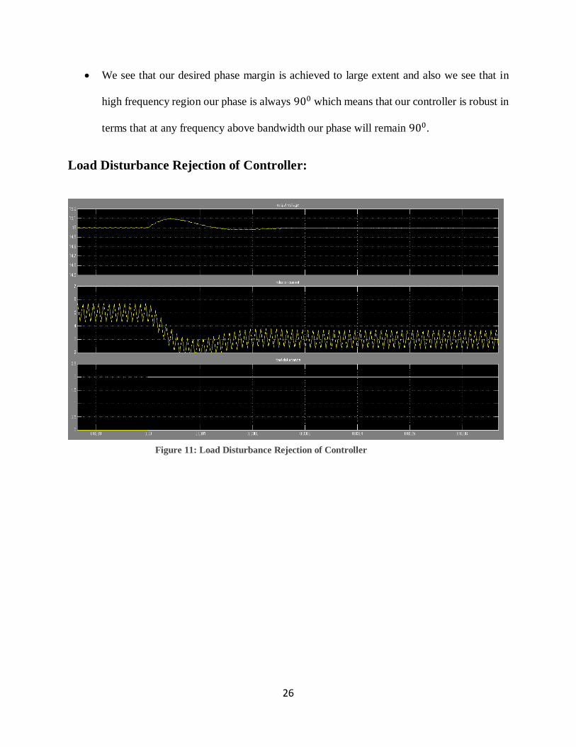
We see that our desired phase margin is achieved to large extent and also we see that in
high frequency region our phase is always 900 which means that our controller is robust in
terms that at any frequency above bandwidth our phase will remain 900.
Load Disturbance Rejection of Controller:
Figure 11: Load Disturbance Rejection of Controller

27
Output Reference Tracking:
4.4 Exact Tuning of the PID Controller:
Motivation:
The main motivation to use this paper is that it helps to design the controller on the combination
of the phase margin with bandwidth and gain margin with phase margin. It also helps to incorporate
the steady state performance. [6]This method also has the advantage of calculating the parameters
by use of pen, paper and the calculator.it can be applied to the systems where the plants exact
model is not known but a little knowledge of the plants bode response will help us out of the
problem.
Objective:
Figure 12: Output Reference Tracking

28
To design a controller that satisfies our requirements of desired frequency response characteristics
in software (Matlab) and also in hardware also with a little error and modification.
4.4.1 Method to Tune: 1. First check for the loop transfer function L(s) should satisfy two constraints:
a) The loop transfer function L(s) should not have any right half plane poles and
strictly proper.
b) The polar plot of the L(𝑗𝜔) for ω≥0 intersects the unit circle and negative semi-real
axis only once.
2. When this is done then we can go for the design:
Standard form of PID controller:
𝐶𝑃𝐼𝐷 = 𝐾𝑃 (1 +1
𝑇𝑖𝑠+ 𝑇𝑑𝑠) …….. (1)
This can be represented in polar form as
𝐶𝑃𝐼𝐷(𝑗𝜔) = 𝑀(𝜔)𝑒𝑗∅(𝜔) …… (2)
Also plant can be represented as
𝐺(𝑗𝜔) = |𝐺(𝑗𝜔)|𝑒𝑗∠𝐺(𝑗𝜔) …….. (3)
3. Now loop transfer function becomes
𝐿(𝑗𝜔) = |𝐺(𝑗𝜔)|𝑀(𝜔)𝑒𝑗(∅(𝜔)+∠𝐺(𝑗𝜔)) ….. (4)
4. Now parameters will be calculated as follows:
𝐾𝑃 = 𝑀𝑔 cos(∅𝑔) ……… (5)
𝑇𝑖 =𝑡𝑎𝑛∅𝑔+√𝑡𝑎𝑛2∅𝑔+4𝜎
2𝜔𝑔𝜎 ……. (6)
𝑇𝑑 = 𝑇𝑖𝜎 …… (7)
Here 𝑀𝑔 = 𝑀(𝜔𝑔)
29
∅𝑔 = 𝑃𝑀 − 𝜋 − ∠𝐺(𝑗𝜔)
𝜎 = degree of freedom= 𝑇𝑑
𝑇𝑖 this ratio affects the position of zeroes of PID
4.4.2 Verification of the Described Method: The above is applied to the buck converter to verify whether the parameter values obtained from
the previous method gives the satisfactory result or not.
Parameter values of the Buck converter:
Inductor (L) =50µH, Output Capacitor(C) =500µF, R=3𝛺, Switching Frequency=100 kHz
Input voltage=28V, Output voltage=15V, Output current=3A
For the above specifications, the control to output transfer function is as follows,
We choose ∅𝑑=520 ,𝑓𝑐 = 5𝑘𝐻𝑧 and we get controller parameters as follows,
For 𝜎−1 = 5,𝐾𝑃 = 6.42,𝑇𝑖 = 2.196 × 10⁻⁴,𝑇𝑑 = 4.393 × 10⁻⁵
For 𝜎−1 = 2, 𝐾𝑃 = 6.42, 𝑇𝑖 = 9.91 × 10⁻⁵, 𝑇𝑑 = 4.95 × 10⁻⁵
For 𝜎−1 = 4, 𝐾𝑃 = 6.42, 𝑇𝑖 = 1.798 × 10⁻⁴, 𝑇𝑑 = 4.5 × 10⁻⁵
4.5 Results From Exact Tuning Method:
0
2 8 6
2.33( )
2.58 10 16.67 10 1
vG s
s sd
30
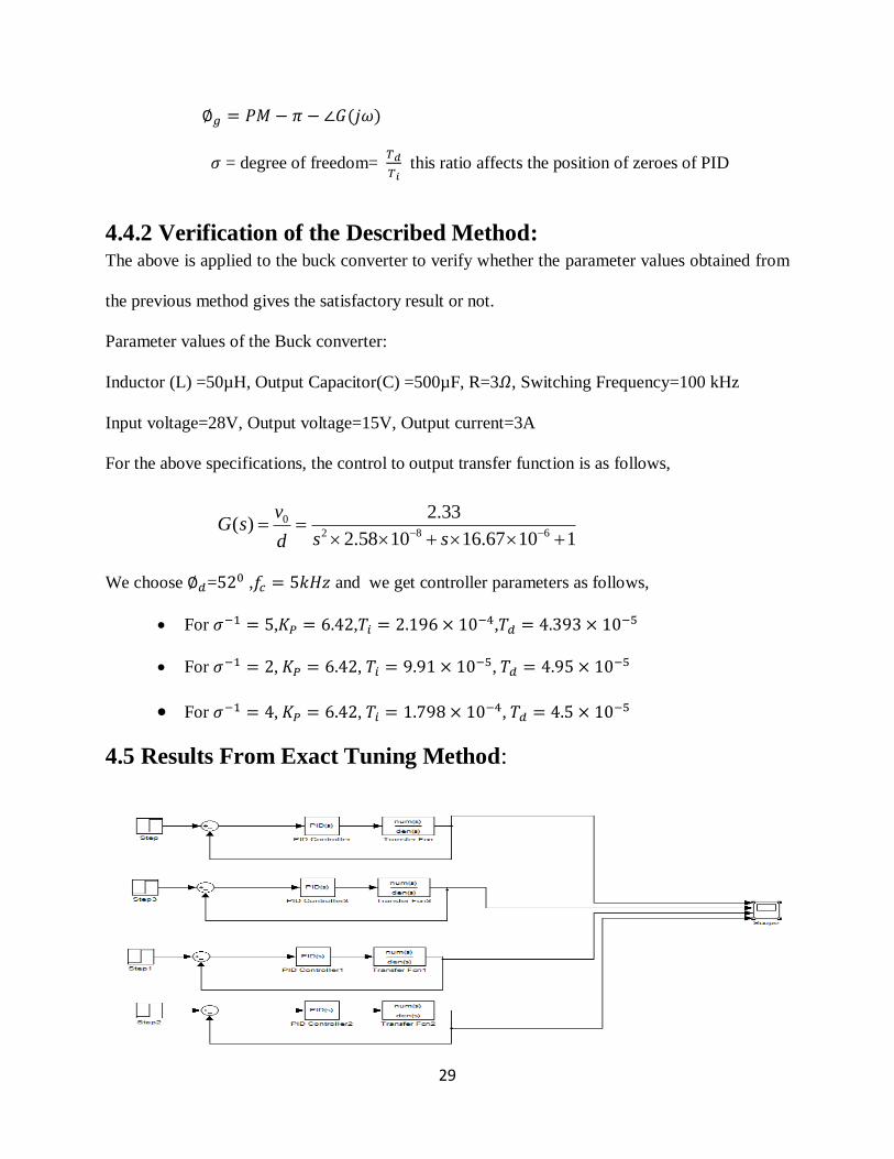
Response of Closed Loop System for Different Values of Degree of Freedom:
Step Response For Different 𝜎−1:
Inference from the figure:
As the value of sigma inverse goes on decreasing, the rise time decreases.
Also the peak overshoots increases.
Settling time increases and also the oscillations in the output start increasing.
This is all because the zeroes of the system first real and as the value of sigma inverse
decreases they become complex conjugate making system oscillatory.
Figure 13: Simulink Model
Figure 14: Step Response for different degree of freedom
31
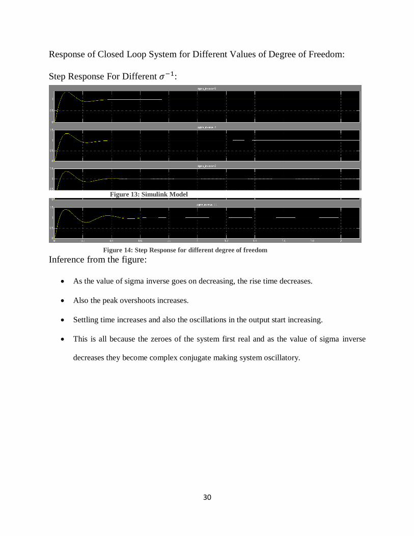
Bode Plots of System with and without PID Controller:
Figure 15: Bode Plots of System with and without PID Controller
32
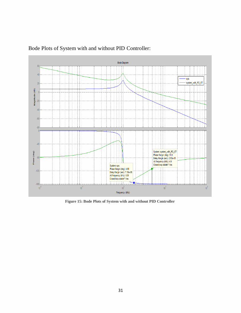
Load disturbance rejection:
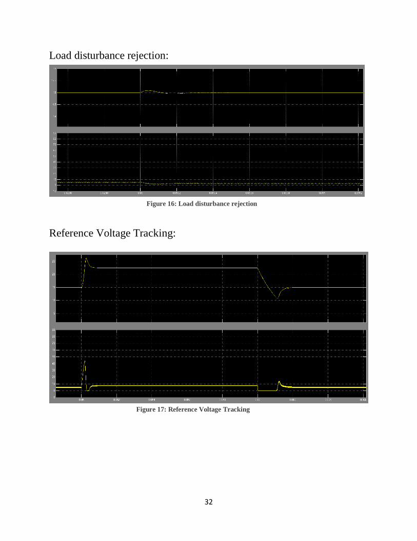
Reference Voltage Tracking:
Figure 16: Load disturbance rejection
Figure 17: Reference Voltage Tracking
33
Limitations:
This cannot be applied to systems having right half poles and zeroes as this is the case with boost
and the buck-boost converters.
4.6 Type III Compensator Design: Type-II compensators are widely used in the compensation for DC-DC converters. [7]But it can
provide maximum phase boost of 900. But if you need the phase boost above 900 then you need
type-III compensator. There are cases when the phase of power stage converter can reach 180
degree, in this case the type-II compensator cannot stabilize the loop. Then the need for the type-
III compensator arises. The extra 900 phase boost provided by the type-III compensator helps to
achieve higher loop crossover frequency than that achievable by the type-II compensator.
Transfer function of type-III compensator,
𝐶(𝑠) =𝑉𝑜(𝑠)
𝑉𝑖(𝑠)=
(𝑠𝐶2𝑅2 + 1)(𝑠𝐶3(𝑅1 + 𝑅3) + 1)
𝑅1(𝐶1 + 𝐶2)𝑠(𝑠𝐶12𝑅2 + 1)(𝑠𝑅3𝐶3 + 1)
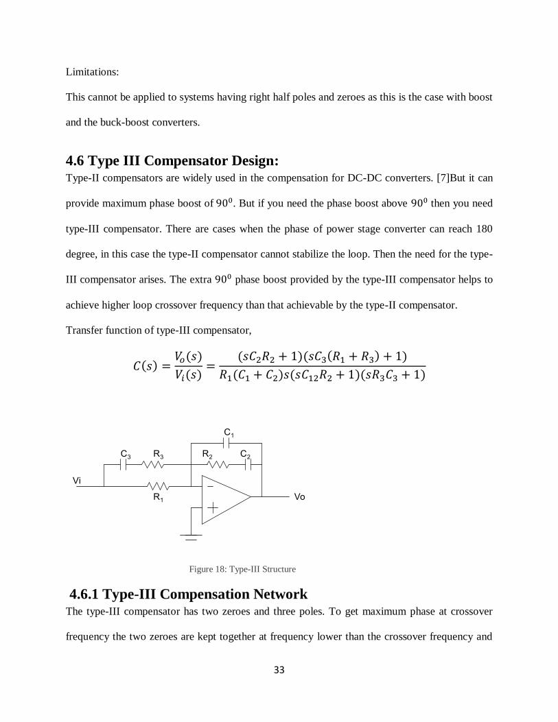
Figure 18: Type-III Structure
4.6.1 Type-III Compensation Network The type-III compensator has two zeroes and three poles. To get maximum phase at crossover
frequency the two zeroes are kept together at frequency lower than the crossover frequency and

34
two poles are kept together at the frequency higher than the crossover frequency, and one pole is
kept at the origin to get the low frequency high gain. Therefore the equivalent transfer function
will become,
𝐶(𝑠) =𝐾 (1 +
𝑠𝜔𝑧
)2
(1 +𝑠
𝜔𝑝)
2
Where pole and zero frequencies are,
𝜔𝑧 =1
𝑅2𝐶2=
1
𝐶3(𝑅1 + 𝑅3)
𝜔𝑝 =1
𝐶12𝑅2=
1
𝐶3𝑅3
Where 𝐶12 =𝐶1𝐶2
(𝐶1+𝐶2) , 𝐾 =
1
𝑅1(𝐶1+𝐶2)
4.6.2 Results From Derived Method:
Application to buck converter:
Parameter values of the Buck converter:
Inductor (L) =50µH, Output Capacitor(C) =500µF, R=3𝛺, Switching Frequency=100 kHz
Input voltage=28V, Output voltage=15V, Output current=3A
For the above specifications, the control to output transfer function is as follows,
We choose ∅𝑑=520 ,𝑓𝑐 = 5𝑘𝐻𝑧 and we get compensator parameters as follows,
R1=5k, R2=9.52k, R3=152, C1=590pF, C2=19.4nF, C3=35.8nF
0
2 8 6
2.33( )
2.58 10 16.67 10 1
vG s
s sd
35
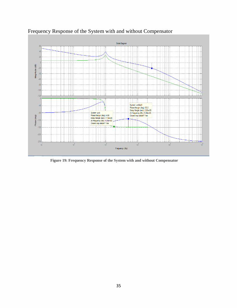
Frequency Response of the System with and without Compensator
Figure 19: Frequency Response of the System with and without Compensator
36
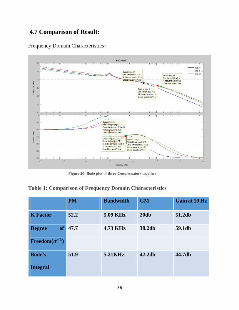
4.7 Comparison of Result:
Frequency Domain Characteristics:
Table 1: Comparison of Frequency Domain Characteristics
PM Bandwidth GM Gain at 10 Hz
K Factor 52.2 5.09 KHz 20db 51.2db
Degree of
Freedom(𝝈−𝟏)
47.7 4.73 KHz 38.2db 59.1db
Bode’s
Integral
51.9 5.21KHz 42.2db 44.7db
Figure 20: Bode plot of three Compensators together

37
Step responses of system with compensators:
Table 2: Comparison of Time Domain Characteristics
Peak Overshoot Rise Time Settling Time
K-Factor 21.6% 33.5µsec 758 µsec
Degree of
Freedom(𝝈−𝟏)
30.9% 36.6 µsec 374 µsec
Bode’s Integral 24.5% 35.6 µsec 167 µsec
Figure 21: Step responses of system with compensators

38
4.8 Experimental Setup:
Experimental Result:
Figure 22: Hardware Image
Figure 23: Hardware Result
39
Conclusion:
The results obtained from these methods are full filling the design criteria and the
set parameters are approximately achieved. So to design the PID these two methods
are quite easy and give satisfactory results. To compare the methods, the solvability
of equation is little bit difficult in Bode’s integral method and more number of
equations need to be solved compared to exact tuning method. But the results
obtained from exact tuning method are best among all these.

40
References:
[1] H. W. Bode, Network Analysis and Feedback Amplifier Design., New York: Van Nostrand, 945..
[2] K. O. M. C. E. 2. edn., Modern Control Engineering. 2nd edn, Prentice Hall, 2000.
[3] S. Samanta, New methods and Models for Simulation and Compensator Design For Buck Converters
in Peak Current Mode Control, Kharagpur: IIT KGP, 2012.
[4] M. K. Kazimierczuk, Pulse-Width Modulated DC-DC power converters, John Wiley and Sons, 2008.
[5] L. a. A. F. Ntogramatzidis, Exact Tuning of PID controllers in control feedback design, IET control
theory & applications 5.4, 2011.
[6] R. W. a. D. M. Erickson, Fundamentals of Power Electronics, Springer, 2001.
[7] A. D. G. a. R. L. Karimi, "PID Controllers Tuning in control feedback design," in Control System
Technolgy, IEEE Transactions, 2003.
[8] L. a. A. P. P. Cao, " "Design Type III Compensator for Power Converters."," in Power Electronics
Technology, 2011.
[9] K. J. a. R. M. M. Aström, Feedback systems: an introduction for scientists and engineers., Princeton
university press, 2010..