Embed Size (px)
Citation preview
COMPARISON OF ASYNCHRONOUS VS. SYNCHRONOUS DESIGN
TECHNOLOGIES USING A 16-BIT BINARY ADDER
by
Michael Brandon Roth
A thesis
submitted in partial fulfillment
of the requirements for the degree of
Masters of Science in Engineering, Electrical Engineering
Boise State University
April, 2004
ii
The thesis presented by Michael Brandon Roth entitled Comparison of
Asynchronous vs. Synchronous Design Technologies using a 16-Bit Binary Adder is
hereby approved:
___________________________________________ R. Jacob Baker Date Advisor
___________________________________________ Scott F. Smith Date Committee Member
___________________________________________ Sin Ming Loo Date Committee Member
___________________________________________ John R. Pelton Date Dean, Graduate College

iii
ACKNOWLEDGMENTS
Without the love and support of the many family and friends this thesis and my
education would not have been possible. I sincerely appreciate all that have contributed
to my education over the years, all of the wonderful teachers and student peers, thank you.
I would especially like to thank Dr. Jake Baker and Tyler Gomm. Dr. Baker,
thank you for your love of teaching, your amazing ability to explain difficult concepts,
and for being there from the beginning of this journey. Tyler, thanks for the support and
encouragement throughout this work, for being an example and always pushing the bar.
To my family, thank you so much for the kind words and encouragement. Thanks,
to my aunts for all their love and support, I can not thank you enough, especially my aunt
Carol for her constant sharing of knowledge and wisdom. To my uncle Bruce, who has
always been there for me, and always offering to help in any possible capacity, a constant
role model in my life.
Thanks to my parents for their continued undying love and support. To my dad
who never ceases to amaze me, and my mom for her amazing motherly qualities and her
ever listening ear. Thanks to my sister Lindsey for putting up with me in the stressful
times, and for all her help.
Finally Charity, thanks for all the love and support, the continued confidence in
me, and the new life lessons I didn’t realize I had left to learn.
iv
ABSTRACT
Asynchronous design is a promising technology that is gaining more and more
attention. It’s claimed to offer several advantages over synchronous designs including
high-speed performance, low power, and modularity.
To compare asynchronous to synchronous design technologies, two 16-bit binary
adders are designed. All design decisions are based on high-speed performance with area
and power as secondary concerns. Architectures are chosen for each adder design that
enables the given technology. The asynchronous design is optimized for the best case
average delay and the synchronous design is optimized for the best worse case delay.
The asynchronous 16-bit adder is implemented with a carry look-ahead architecture using
2-bit blocks. The carry-select architecture is selected for implementing the synchronous
16-bit adder.
The two 16-bit adder designs are compared using two experiments. The first
experiment measures the computation delay for 10,000 random input permutations. The
synchronous design worse case delay is compared to the asynchronous average delay.
The asynchronous adder average delay outperforms the synchronous worse case delay by
more than 250 ps. In the second experiment the 16-bit binary adders are implemented
into an adder test-bench system, and 32 consecutive additions are performed. In this
experiment the synchronous adder design has a better computation delay by
approximately 500 ps per addition. In the adder test-bench system the asynchronous
adder performance realizes the full overhead delay associated with an asynchronous
implementation.
v
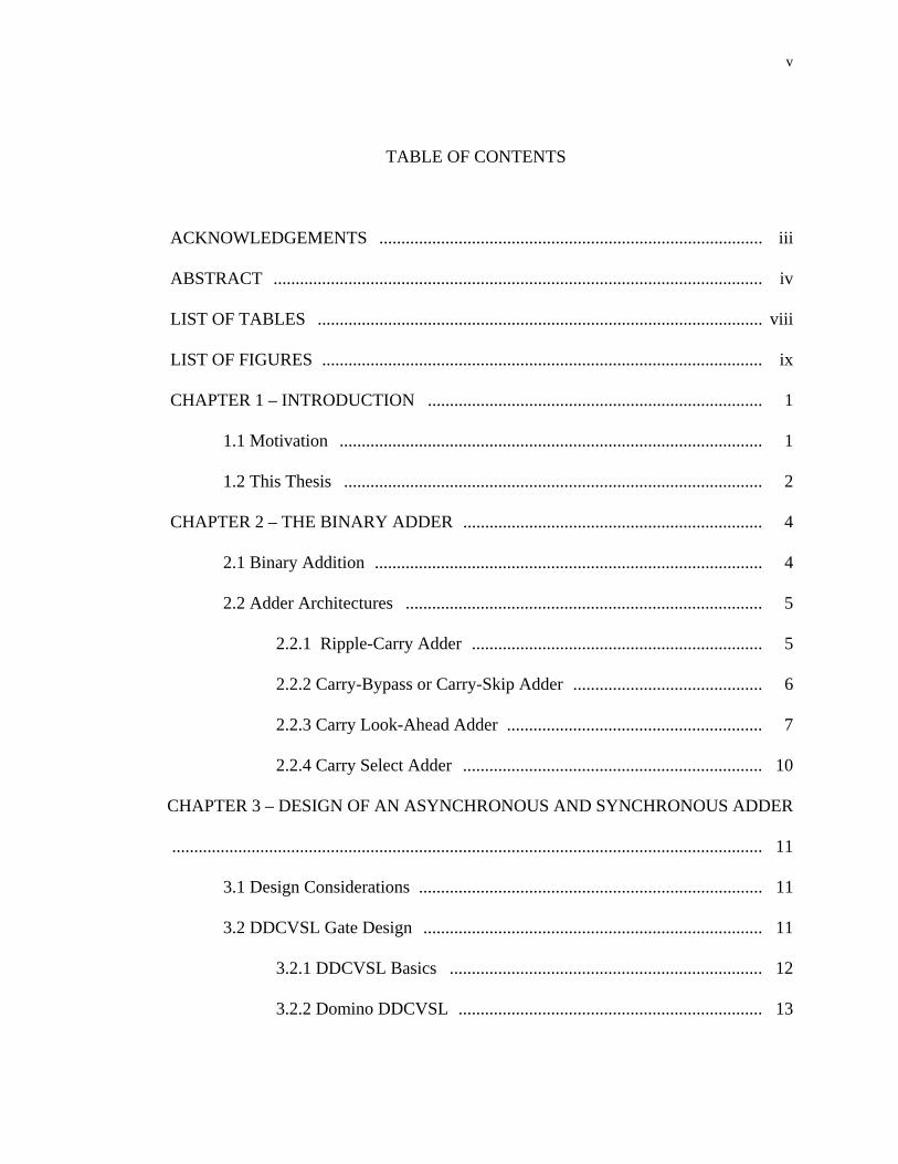
TABLE OF CONTENTS
ACKNOWLEDGEMENTS ....................................................................................... iii
ABSTRACT ............................................................................................................... iv
LIST OF TABLES ..................................................................................................... viii
LIST OF FIGURES .................................................................................................... ix
CHAPTER 1 – INTRODUCTION ............................................................................ 1
1.1 Motivation ................................................................................................ 1
1.2 This Thesis ............................................................................................... 2
CHAPTER 2 – THE BINARY ADDER .................................................................... 4
2.1 Binary Addition ........................................................................................ 4
2.2 Adder Architectures ................................................................................. 5
2.2.1 Ripple-Carry Adder .................................................................. 5
2.2.2 Carry-Bypass or Carry-Skip Adder ........................................... 6
2.2.3 Carry Look-Ahead Adder .......................................................... 7
2.2.4 Carry Select Adder .................................................................... 10
CHAPTER 3 – DESIGN OF AN ASYNCHRONOUS AND SYNCHRONOUS ADDER
...................................................................................................................................... 11
3.1 Design Considerations .............................................................................. 11
3.2 DDCVSL Gate Design ............................................................................. 11
3.2.1 DDCVSL Basics ....................................................................... 12
3.2.2 Domino DDCVSL ..................................................................... 13
vi
3.2.3 Designing DDCVSL ................................................................. 14
3.2.3.1 DDCVSL Tree Design ............................................... 14
3.2.3.2 Precharge and Restore Sizing ..................................... 15
3.2.3.3 High-Skew Inverter .................................................... 17
3.2.4 Example DDCVSL Design ....................................................... 17
3.3 Asynchronous Adder Design ................................................................... 19
3.3.1 Architecture ............................................................................... 20
3.3.1.1 Single-Level CLA ...................................................... 21
3.3.1.1.1 2-Bit CLA Design ....................................... 22
3.3.1.1.2 2-Bit CLA Design with Complement Carry
Generate ..................................................................... 25
3.3.1.2 Multi-level or Treed CLA .......................................... 28
3.3.1.3 Manchester Carry Chain ............................................. 30
3.3.1.4 Architecture Experiment ............................................. 31
3.3.2 Asynchronous Communication Design ..................................... 33
3.3.2.1 Communication Control Logic ................................... 34
3.3.2.2 Completion Detection Circuit .................................... 38
3.3.3 Asynchronous 16-Bit Adder ...................................................... 42
3.3.4 Enhanced Asynchronous 16-Bit Adder ..................................... 44
3.4 Synchronous Adder Design ...................................................................... 45
3.4.1 Architecture ............................................................................... 46
3.4.2 Carry-Select Adder Design ....................................................... 46
3.4.2.1 2-Bit CLA Design Assuming Carry-in ....................... 47
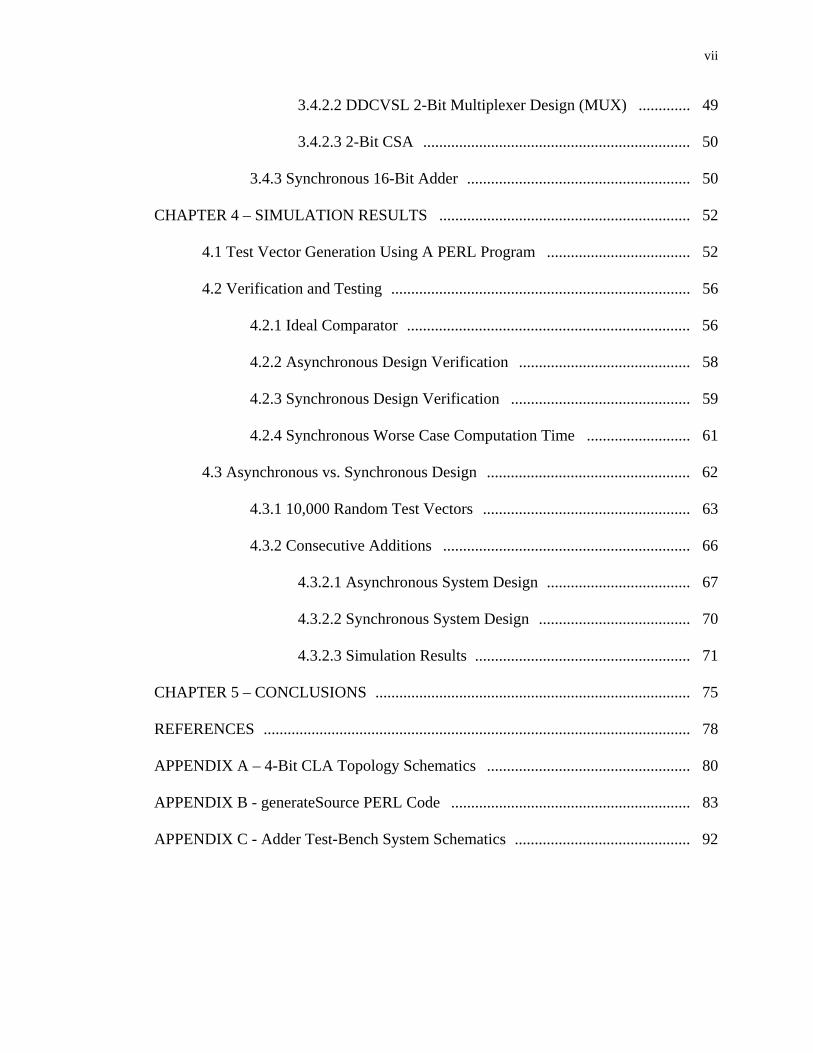
vii
3.4.2.2 DDCVSL 2-Bit Multiplexer Design (MUX) ............. 49
3.4.2.3 2-Bit CSA ................................................................... 50
3.4.3 Synchronous 16-Bit Adder ........................................................ 50
CHAPTER 4 – SIMULATION RESULTS ............................................................... 52
4.1 Test Vector Generation Using A PERL Program .................................... 52
4.2 Verification and Testing ........................................................................... 56
4.2.1 Ideal Comparator ....................................................................... 56
4.2.2 Asynchronous Design Verification ........................................... 58
4.2.3 Synchronous Design Verification ............................................. 59
4.2.4 Synchronous Worse Case Computation Time .......................... 61
4.3 Asynchronous vs. Synchronous Design ................................................... 62
4.3.1 10,000 Random Test Vectors .................................................... 63
4.3.2 Consecutive Additions .............................................................. 66
4.3.2.1 Asynchronous System Design .................................... 67
4.3.2.2 Synchronous System Design ...................................... 70
4.3.2.3 Simulation Results ...................................................... 71
CHAPTER 5 – CONCLUSIONS ............................................................................... 75
REFERENCES ........................................................................................................... 78
APPENDIX A – 4-Bit CLA Topology Schematics ................................................... 80
APPENDIX B - generateSource PERL Code ............................................................ 83
APPENDIX C - Adder Test-Bench System Schematics ............................................ 92
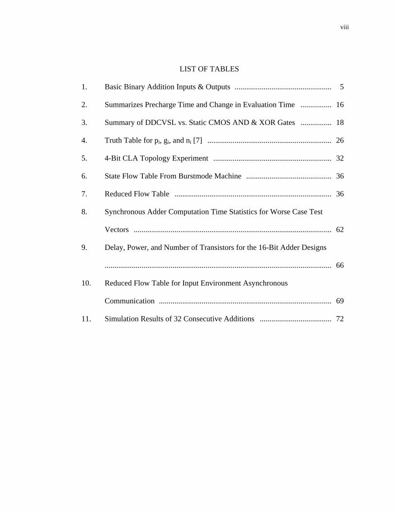
viii
LIST OF TABLES
1. Basic Binary Addition Inputs & Outputs .................................................. 5
2. Summarizes Precharge Time and Change in Evaluation Time ................ 16
3. Summary of DDCVSL vs. Static CMOS AND & XOR Gates ................ 18
4. Truth Table for pi, gi, and ni [7] ................................................................ 26
5. 4-Bit CLA Topology Experiment ............................................................. 32
6. State Flow Table From Burstmode Machine ............................................ 36
7. Reduced Flow Table ................................................................................. 36
8. Synchronous Adder Computation Time Statistics for Worse Case Test
Vectors ...................................................................................................... 62
9. Delay, Power, and Number of Transistors for the 16-Bit Adder Designs
..................................................................................................................... 66
10. Reduced Flow Table for Input Environment Asynchronous
Communication ......................................................................................... 69
11. Simulation Results of 32 Consecutive Additions ..................................... 72
ix
LIST OF FIGURES
1. Full Adder Block Diagram ........................................................................ 4
2. Ripple Carry Adder (RCA) Block Diagram ............................................. 6
3. Carry Bypass Block Diagram ................................................................... 7
4. Carry Look-Ahead Block Diagram ........................................................... 8
5. Carry Select Adder Block Diagram .......................................................... 10
6. DDCVSL Block Diagram [13] ................................................................. 13
7. DDCVSL Implementation of (a) AND and (b) XOR ............................... 18
8. DDCVSL Tree Implementation of (a) Carry0 and (b) Carry1 ................. 23
9. DDCVSL Schematics for (a) Carry0 and (b) Carry1 ................................ 24
10. 2-Bit CLA Schematic ................................................................................ 25
11. (a) Carry0 and (b) Carry1 Implemented with n (complement carry
generate) .................................................................................................... 27
12. Block Diagram of Multi-Level CLA using Group Generate and Propagate
..................................................................................................................... 29
13. Manchester Carry Chain Schematic [7] .................................................... 30
14. Asynchronous Burstmode Maching for 16-Bit Adder .............................. 35
15. Asynchronous Communication Control Logic ......................................... 37
16. Two Completion Detection Implementations (a) Johnson’s Dynamic Design
[1] (b) Static Design .................................................................................. 39
17. Dynamic Completion Detector with Parallel Structure ............................ 41
x
18. Results of Three Completion Detection Circuits using Four Test
Conditions ................................................................................................. 41
19. Asynchronous 16-Bit Adder Schematic .................................................... 43
20. Enhanced Asynchronous 16-Bit Adder with Carry-Bypass ..................... 45
21. Schematic for Carry1 when assuming carry-in is (a) low and (b) high .... 48
22. DDCVSL 2-Bit MUX ............................................................................... 49
23. 2-Bit CSA Schematic ................................................................................ 50
24. Synchronous 16-Bit Adder Schematic ...................................................... 51
25. Sources Generated by PERL Program for All Permutations of 5 Bits ..... 54
26. 32 Random Inputs Generated by PERL Program for 5 Binary Sources ... 55
27. Verification Results Using An Ideal Comparator ..................................... 57
28. Simulation Verification Results for 2-Bit CLA ........................................ 58
29. Synchronous 2-Bit CSA Verification ....................................................... 60
30. Histogram Comparing the Enhanced Asynchronous and Asynchronous
16-bit Adder Designs ................................................................................ 63
31. Asynchronous vs. Synchronous Histogram of Computation Delay ......... 64
32. Burstmode Machine for Input Environment Asynchronous Communication
..................................................................................................................... 68
33. Input Environment Asynchronous Communication Logic ....................... 69
34. Asynchronous Adder Test-Bench System ................................................ 70
35. Clocking Scheme for the Synchronous Adder System ............................. 71
1
CHAPTER 1 - INTRODUCTION
1.1 Motivation
Asynchronous design is a promising technology that is gaining more and more
attention. A vast majority of the literature that reviews asynchronous and synchronous
design methods finds that an asynchronous design has several potential advantages over a
synchronous design. Others are critics of asynchronous designs and either claim there are
no advantages, or that an asynchronous design only has advantages in a small subset of
circumstances.
Asynchronous is an emerging circuit design technology that has promise for low
power and high-speed [1]. The idea behind the high-speed operation is asynchronous
circuits operate at average rates of operation, and synchronous circuits are required to
operate at worst case rates. A synchronous circuit is governed by a clock, which is set to
a frequency equal to the worse case delay of the circuit. An asynchronous circuit is not
controlled by a clock, and instead uses a completion detector to detect when it is
complete. Using the completion detector overtime, the asynchronous circuit approaches
an average rate of operation. Lower power is associated with an asynchronous design
due to the basic premise of reduced clock switching [2]. In synchronous digital circuits
the clocking infrastructure uses 20-40% of the total power [2]. As the complexity of
integrated circuits increase, global clock distribution becomes more and more difficult.
An asynchronous design is a solution to the clock distribution problem [2][3]. Another
advantage of an asynchronous design is it allows for modularity [4]. An asynchronous
2
design that is delay-insensitive can be placed into any system design as a module without
adjusting internal timing to accommodate the new system design [3].
An article by Kinniment suggests that asynchronous designs only improve
average propagation time based on random inputs, but have limited performance benefits
when associated with a smaller set of conditions [5]. He argues that most circuit
implementations are not going to be subject to random inputs, but rather on average will
consist of some smaller subset. Fu-Chiung argues that Kinniment uses an unfair
comparison by comparing an asynchronous version of a ripple-carry adder to a
synchronous tree-like conditional sum adder [6]. In addition, Ruiz points out
Kinniment’s study only investigated asynchronous methods using standard gates and did
not include modifications, which might enhance or enable the asynchronous
performance [7].
1.2 This Thesis
This thesis investigates asynchronous vs. synchronous design technologies using
two 16-bit binary adders. An adder architecture and logic style is selected for each
design that enables the given design technology, asynchronous or synchronous to achieve
the best performance. The 16-bit adder designs will be compared using computation time,
number of transistors, and power. The adders will be tested using 10,000 random inputs.
This experiment demonstrates that the asynchronous design outperforms the synchronous
design on all but a small subset of input conditions. In addition, to evaluate the adders
performance both designs are implemented into an adder test-bench system, and 32
consecutive additions performed.
3
The binary adder is used as the vehicle for comparison for two reasons. First, it is
a very relevant design. It is one of the most significant operations in any computing
system [1]. The binary adder is a basic building block in a processor design, and is used
to implement other complex functions like multiplication and division. A frequently used
module in a system has greater influences on overall performance. In one RISC
processor implementation 72% of all instructions use addition [4].
The second reason for using the binary adder in the comparison of asynchronous
and synchronous technologies is that the binary adder’s computation time is very data-
dependent. In order for an asynchronous system to have any benefit over a synchronous
implementation the system must exhibit a data-dependent delay [1]. For these two
reasons much of the work in the asynchronous literature uses the binary adder for
comparing asynchronous to synchronous design technologies [3][4][5][6].
Throughout the design process all simulations are run using Micron Technology’s
0.11 µm process models with typical n-channel and p-channel drive, a 2.5 V power
supply, and a worse case temperature of 85 ºC. In the schematics all logic is designed
using a minimum gate width of 12 µm and a minimum length of 1 µm. The effective
transistor sizing is adjusted for the 0.11 µm process using a shrink factor, which is not
reported here for proprietary protection. For equal rising and falling transitions a P to N
ratio of 2 is used (minimum sized inverter is 24/12).
4
CHAPTER 2 - THE BINARY ADDER
2.1 Binary Addition
Digital computers use the binary number system, which is composed of only two
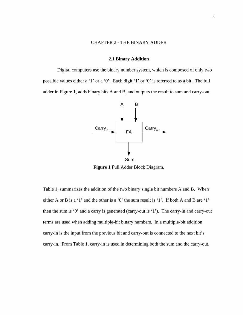
possible values either a ‘1’ or a ‘0’. Each digit ‘1’ or ‘0’ is referred to as a bit. The full
adder in Figure 1, adds binary bits A and B, and outputs the result to sum and carry-out.
FA
A B
Sum
CarryoutCarryin
Figure 1 Full Adder Block Diagram.
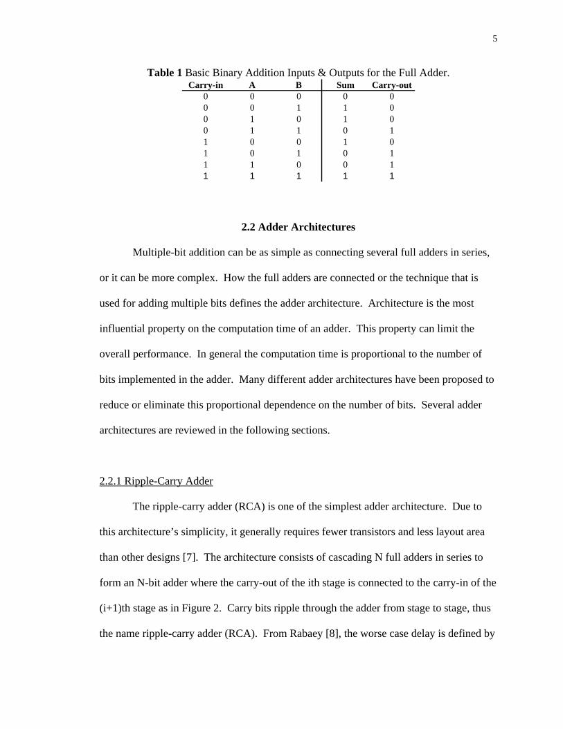
Table 1, summarizes the addition of the two binary single bit numbers A and B. When
either A or B is a ‘1’ and the other is a ‘0’ the sum result is ‘1’. If both A and B are ‘1’
then the sum is ‘0’ and a carry is generated (carry-out is ‘1’). The carry-in and carry-out
terms are used when adding multiple-bit binary numbers. In a multiple-bit addition
carry-in is the input from the previous bit and carry-out is connected to the next bit’s
carry-in. From Table 1, carry-in is used in determining both the sum and the carry-out.
5
Table 1 Basic Binary Addition Inputs & Outputs for the Full Adder. Carry-in A B Sum Carry-out
0 0 0 0 00 0 1 1 00 1 0 1 00 1 1 0 11 0 0 1 01 0 1 0 11 1 0 0 11 1 1 1 1
2.2 Adder Architectures
Multiple-bit addition can be as simple as connecting several full adders in series,
or it can be more complex. How the full adders are connected or the technique that is
used for adding multiple bits defines the adder architecture. Architecture is the most
influential property on the computation time of an adder. This property can limit the
overall performance. In general the computation time is proportional to the number of
bits implemented in the adder. Many different adder architectures have been proposed to
reduce or eliminate this proportional dependence on the number of bits. Several adder
architectures are reviewed in the following sections.
2.2.1 Ripple-Carry Adder
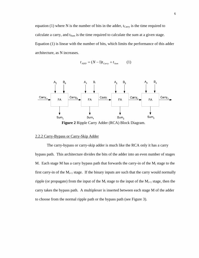
The ripple-carry adder (RCA) is one of the simplest adder architecture. Due to
this architecture’s simplicity, it generally requires fewer transistors and less layout area
than other designs [7]. The architecture consists of cascading N full adders in series to
form an N-bit adder where the carry-out of the ith stage is connected to the carry-in of the
(i+1)th stage as in Figure 2. Carry bits ripple through the adder from stage to stage, thus
the name ripple-carry adder (RCA). From Rabaey [8], the worse case delay is defined by
6
equation (1) where N is the number of bits in the adder, tCarry is the time required to
calculate a carry, and tSum is the time required to calculate the sum at a given stage.
Equation (1) is linear with the number of bits, which limits the performance of this adder
architecture, as N increases.
SumCarryADD ttNt +−= )1( (1)
Figure 2 Ripple Carry Adder (RCA) Block Diagram.
2.2.2 Carry-Bypass or Carry-Skip Adder
The carry-bypass or carry-skip adder is much like the RCA only it has a carry
bypass path. This architecture divides the bits of the adder into an even number of stages
M. Each stage M has a carry bypass path that forwards the carry-in of the Mi stage to the
first carry-in of the Mi+1 stage. If the binary inputs are such that the carry would normally
ripple (or propagate) from the input of the Mi stage to the input of the Mi+1 stage, then the
carry takes the bypass path. A multiplexer is inserted between each stage M of the adder
to choose from the normal ripple path or the bypass path (see Figure 3).
7
Figure 3 Carry Bypass Block Diagram.
In the figure the inputs to each full adder block are carry generate (gi) and carry
propagate (pi). These signals will be discussed in more detail in the carry look-ahead
adder discussion. When a bypass occurs it allows the Mi+1 stage to start evaluating sums
instead of waiting for the ith stage to ripple the carry through each bit of the stage. The
worse case delay of the CBA is defined by equation (2).
SumBypassCarrySetupADD ttMtM
Ntt +−+−
+= )1()1
( (2)
Where N is the number of bits in the adder, and M is the number of stages. tcarry and tsum
are the times to compute a carry and sum. tbypass is the time to bypass a carry to the next
stage, and tsetup is the time it takes to calculate carry propagate and generate. The worse
case delay is decreased compared to the RCA, but the speed is still linear with the
number of bits implemented in the adder architecture.
2.2.3 Carry Look-Ahead Adder
The carry look-ahead architecture reduces the delay dependence on the number of
bits by using a parallel structure. Instead of rippling the carry through all stages (bits) of
the adder, it calculates all carrys in parallel based on equation (3).
8
1−+= iiii CpgC (3)
In equation (3) the gi and pi terms are defined as carry generate and carry propagate for
the ith bit. If carry generate is true then a carry is generated at the ith bit. If carry
propagate is true then the carry-in to the ith bit is propagated to the carry-in of i+1 bit.
They are defined by equations (4) and (5) where Ai and Bi are the binary inputs being
added.
iii BAg = (4)
iii BAp ⊕= (5)
Using the carry generate and carry propagate signals and the carry equation defined in
equation (3) the CLA architecture takes advantage of parallelism.
Figure 4 Carry Look-Ahead Block Diagram.
Figure 4 is a block diagram of a 4-bit CLA structure. As can been seen in the
figure the propagates and generates are calculated in parallel for each bit. Then using the
carry generate and propagate information each carry bit is calculated (in parallel), and
finally in this block diagram the carrys are feedback and all the sums are calculated in
9
parallel. At a first glance it appears the CLA architecture computation time is
independent of the number of bits in the adder design. Equation (6) defines the
computation delay of a CLA.
sumcarrypgadd tttt ++= (6)
Where tpg is the time to compute carry generate and propagate, tcarry is the longest carry
computation time, and tsum is the time to calculate the sum. Equation (6) supports that the
CLA computation time is independent on the number of bits in the adder design, since N
(the number of bits in adder) does not appear in the equation.
CLA architectures are typically implemented using blocks of CLA structures
connected together, because one structure is not practical due to large fan-in [1]. This
makes sense if the carry equation (Eq. 3) is analyzed more closely. As the number of bits
implemented in the CLA increases the terms in the carry equation grow. This increases
the fan-in to the carry logic, as seen in the example below when the carry equation is
expanded.
in
in
CarryppgpgCpgCCarrypgC
010110111
000
++=+=+=
This increase in fan-in actually makes the CLA computation time dependent on the
number of bits in an adder. In addition, the fan-in limits the number of bits that can be
implemented in a given CLA. To design a CLA architecture, the adder is divided into
CLA blocks and then the blocks are cascaded to form the full adder. The CLA blocks
can be cascaded using several different approaches to optimize the design.
10
2.2.4 Carry Select Adder
The Carry Select or Conditional Sum architecture is considered the fastest
synchronous type adder [4]. Figure 5 illustrates a block diagram for a 2-bit slice.
Figure 5 Carry Select Adder Block Diagram.
In many architectures, including those already discussed, higher-order bits within the
architecture must wait for the carry from the lower order bits before computing the results.
To completely eliminate the data dependence this architecture computes both possible
values of sum and carry-out for both a carry-in of zero and one. As shown in Figure 5,
once the carry-in arrives the correct sum and carry-out are selected from a multiplexer
(MUX). Equation (7) defines the delay of the CSA architecture, where tsetup is the time to
compute the initial carry and tmux is the time for the MUX to select and pass an input.
summuxsetupadd tNttt ++= (7)
This architecture greatly reduces the computation time’s dependence on both the binary
data and the number of bits in the adder design.
11
CHAPTER 3 - DESIGN OF AN ASYNCHRONOUS AND SYNCHRONOUS ADDER
3.1 Design Considerations
Two 16-bit binary adders are designed to compare asynchronous to synchronous
design technologies. All design decisions are based on high-speed with area (number of
transistors) and power as secondary concerns. The most influential design decisions on
adder performance are the adder architecture, and the logic style used to implement the
adder designs.
In designing the two adders the number of variables between the two designs is
kept to a minimum to ensure the differences observed are due to the design technology,
synchronous or asynchronous. For example, using identical architectures for both the
asynchronous and the synchronous adders could be considered as part of this requirement.
However, if the architecture gives an advantage and is more suitable to either design
technology, then the architecture can be considered as specific to the design technology.
Using different architectures then doesn’t introduce a secondary variable between the two
adder designs.
3.2 DDCVSL Gate Design
The design requirements for the logic style used to realize the adder designs are
high-speed, and differential (dual-rail). Domino differential cascode voltage switch logic
(DDCVSL) is a logic style that meets these requirements. DDCVSL is very popular in
several of the asynchronous papers [1][3][7][9]. Johnson and Ruiz point out that
DDCVSL naturally leads to a delay-insensitive design due to the ease of detecting
12
completion using the differential signals [1][7]. The dual-rail property is also useful for
providing differential inputs to the exclusive-OR (XOR) gates that are used in adder
designs to implement both the propagate and sum logic.
In a couple papers the performance of DDCVSL was compared to other logic
styles [10][13]. Chu and Pulfrey compared both static and dynamic logic styles using full
adder designs [10]. They found that DCVSL offered the best speed performance at a cost
of power.
3.2.1 DDCVSL Basics
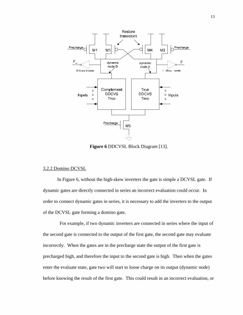
Figure 6 is a block diagram of a domino DCVSL (DDCVSL) gate. From the
figure, when the precharge signal is low the DDCVSL gate is in the precharge state
where the internal dynamic nodes are charged to VDD through transistors M1 and M2.
When precharge transitions high the precharge transistors are off, and the tree is in the
evaluate state. The dynamic nodes float until one of the DDCVSL trees evaluates and
pulls the corresponding dynamic node low through transistor M5, the evaluation or foot
transistor. Then one of the restore transistors either M3 or M4 pulls the opposite tree
back high if any charge sharing occurred between the dynamic node and nodes within the
off tree. The restore is important to ensure that the inverter connected to the off tree is
fully driving a low. The inverters are skewed with a sizing that makes the rising
transition faster (larger P:N ratio). Sizing the p-channel larger with a minimum n-channel
sizing allows for more of the input capacitance of the inverter to be dedicated to driving
the output high.
13
Figure 6 DDCVSL Block Diagram [13].
3.2.2 Domino DCVSL
In Figure 6, without the high-skew inverters the gate is simple a DCVSL gate. If
dynamic gates are directly connected in series an incorrect evaluation could occur. In
order to connect dynamic gates in series, it is necessary to add the inverters to the output
of the DCVSL gate forming a domino gate.
For example, if two dynamic inverters are connected in series where the input of
the second gate is connected to the output of the first gate, the second gate may evaluate
incorrectly. When the gates are in the precharge state the output of the first gate is
precharged high, and therefore the input to the second gate is high. Then when the gates
enter the evaluate state, gate two will start to loose charge on its output (dynamic node)
before knowing the result of the first gate. This could result in an incorrect evaluation, or
14
in an asynchronous implementation early completion detection. The domino technique
solves this problem by adding an inverter to the output of the dynamic gate, so that the
inputs to successive dynamic gates in a network are all low during precharge [8]. The
basic idea of domino is to only allow 0→1 transitions on the inputs of dynamic logic
during the evaluate state. As the inputs of each successive gate rise there is a falling
domino effect.
3.2.3 Designing DDCVSL
DDCVSL gate design involves determining the transistor arrangement and size in
the DDCVSL tree, sizing the precharge, restore, and foot (evaluate) transistors, and sizing
the high-skew inverter to drive the output load.
3.2.3.1 DDCVSL Tree Design
The DDCVSL tree design involves sizing and arranging the transistors to realize
the intended function. The function can be realized directly by connecting n-channel
transistors that reflect the function in the true tree, and the complement of the function in
the complement tree.
Three things need to be considered when design the DDCVSL trees.
1. When possible transistors with the same input signal within the same tree or between the true and complement trees should be combined or shared.
2. The number of transistors connected to the dynamic node should be kept to a minimum to reduce the output capacitance.
3. Transistors with input signals that transition after other input signals within the same stack should be moved up the stack if possible.
15
By sharing transistors within or between trees the total number of transistors in the
overall design is reduced. Minimizing the capacitance on the dynamic node enables
faster evaluation times. The fewer devices connected to the dynamic nodes the better.
To demonstrate the proper tree connection equation (8) is realized.
)( CBAF += (8)
Transistor A should be connected to the dynamic node with B and C connected to the
source of A, instead of connecting both B and C to the dynamic node and then connecting
A to the sources of B and C. If an input is more likely to reach the DDCVSL gate last it
should be connected higher in the tree for two reasons. One faster operation will occur
because everything below it has already evaluated, and two if the tree ends up not
evaluating it reduces the voltage level the restore device must restore.
All the devices in the trees are sized the same so that longest stack of transistors
connected in series is equivalent to the minimum n-channel device width of 12 µm [12].
The foot or evaluate transistor is sized 1.5 times the size of the transistors in the tree [12].
3.2.3.2 Precharge and Restore Sizing
The sizing of the precharge and restore transistors are governed by the same
principles. Both the precharge and the restore transistors are directly connected to the
dynamic nodes. The larger the precharge and restore transistors the larger the
capacitance on the dynamic node, which decreases evaluation time. The goal is to size
the precharge and restore transistors large enough to reduce the precharge and restore
time, with the smallest affect on evaluation time. Basically, find the point of diminishing
returns skewed in favor of the evaluation time.
16
The evaluation time of each DDCVSL gate is more critical than the precharge time. In
the asynchronous case a portion of the precharge time will be hidden during the
asynchronous handshaking, and in the synchronous case the only precharge requirement
is that the precharge time be less than the evaluation time (clock high vs. clock low time).
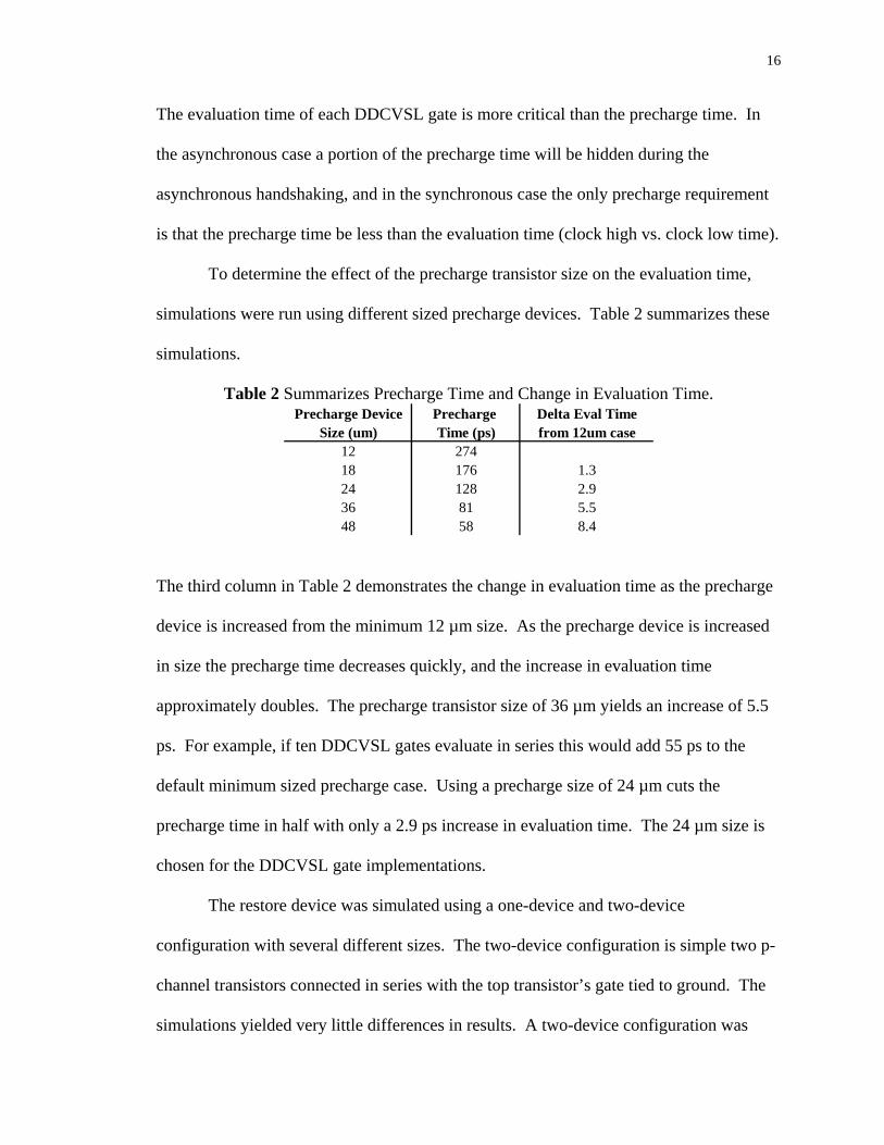
To determine the effect of the precharge transistor size on the evaluation time,
simulations were run using different sized precharge devices. Table 2 summarizes these
simulations.
Table 2 Summarizes Precharge Time and Change in Evaluation Time. Precharge Device Precharge Delta Eval Time
Size (um) Time (ps) from 12um case12 27418 176 1.324 128 2.936 81 5.548 58 8.4
The third column in Table 2 demonstrates the change in evaluation time as the precharge
device is increased from the minimum 12 µm size. As the precharge device is increased
in size the precharge time decreases quickly, and the increase in evaluation time
approximately doubles. The precharge transistor size of 36 µm yields an increase of 5.5
ps. For example, if ten DDCVSL gates evaluate in series this would add 55 ps to the
default minimum sized precharge case. Using a precharge size of 24 µm cuts the
precharge time in half with only a 2.9 ps increase in evaluation time. The 24 µm size is
chosen for the DDCVSL gate implementations.
The restore device was simulated using a one-device and two-device
configuration with several different sizes. The two-device configuration is simple two p-
channel transistors connected in series with the top transistor’s gate tied to ground. The
simulations yielded very little differences in results. A two-device configuration was
17
chosen with each transistor sized with the minimum sizing of 12 µm/1 µm, which gives
an effective size of 6 µm/1 µm. This smaller device is desirable to reduce the current.
By implementing the restore device using two devices instead of a single 12 µm/2 µm
transistor the capacitance on the dynamic node is reduced [12].
3.2.3.3 High-Skew Inverter
The high-skew inverter is sized in favor of the inverter output transitioning high,
the evaluate case. Therefore the p-channel is the skewed device. The n-channel is sized
with the minimum device size of 12 µm/1 µm (width/length). The p-channel is sized
based on the amount of output load. The minimum p-channel size used in the adder
designs for the skewed inverter is 36 µm/1 µm.
3.2.4 Example DDCVSL Design
The AND and XOR functions are two basic gates that will be used to calculate
generate and propagate terms in the adder designs. These logic functions were
implemented directly into the DDCVSL trees in Figure 7. The gates were designed using
the DDCVSL design discussion.
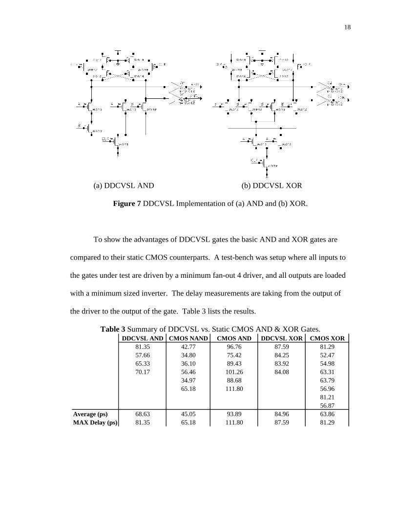
18
(a) DDCVSL AND (b) DDCVSL XOR
Figure 7 DDCVSL Implementation of (a) AND and (b) XOR.
To show the advantages of DDCVSL gates the basic AND and XOR gates are
compared to their static CMOS counterparts. A test-bench was setup where all inputs to
the gates under test are driven by a minimum fan-out 4 driver, and all outputs are loaded
with a minimum sized inverter. The delay measurements are taking from the output of
the driver to the output of the gate. Table 3 lists the results.
Table 3 Summary of DDCVSL vs. Static CMOS AND & XOR Gates. DDCVSL AND CMOS NAND CMOS AND DDCVSL XOR CMOS XOR
81.35 42.77 96.76 87.59 81.2957.66 34.80 75.42 84.25 52.4765.33 36.10 89.43 83.92 54.9870.17 56.46 101.26 84.08 63.31
34.97 88.68 63.7965.18 111.80 56.96
81.2156.87
Average (ps) 68.63 45.05 93.89 84.96 63.86MAX Delay (ps) 81.35 65.18 111.80 87.59 81.29
19
The DDCVSL AND gate is compared to the static CMOS NAND and static CMOS AND
equivalent. The static CMOS AND is implemented using a NAND gate with an inverter.
Comparing DDCVSL AND to the equivalent CMOS AND demonstrates the high-speed
nature of DDCVSL. The DDCVSL XOR gate is slower than the static CMOS gate,
however the DDCVSL gate has differential inputs. If an inverter delay is added to the
static CMOS XOR gate delays, then the DDCVSL gate has a better average and worse
case delay. Notice that all possible permutations of input sequences that cause the output
to switch were tested. For the DDCVSL there are only four possibilities, because the
output always starts out at the same state, since this is a precharged gate. The CMOS
gates on the other hand have more permutations of inputs to test, which are based on the
previous state of the output.
3.3 Asynchronous Adder Design
The asynchronous 16-bit adder design involves selecting and designing the best
architecture for an asynchronous technology, and designing the asynchronous
communication logic. All logic is designed for high-speed operation. The asynchronous
communication design is critical to the overall performance of the asynchronous adder.
As Nowick and others point out, asynchronous circuits have the potential to outperform
synchronous designs on average inputs [9]. However, if the asynchronous methods incur
significant overhead the potential benefits of the asynchronous design will be undercut.
20
3.3.1 Architecture
The asynchronous adder architecture needs to exhibit several characteristics,
which include high-speed, and the ability to take advantage of an asynchronous
implementation. Asynchronous circuits have the potential to operate at an average delay.
Therefore, selecting a high-speed architecture for the asynchronous design involves
selecting an architecture that improves the average delay of the adder. Several
asynchronous articles use the carry look-ahead (CLA) architecture for implementing
asynchronous adders [1][4][6][7]. The CLA reduces the linear dependence on the
number of bits implemented in the adder, and improves the average computation delay.
The CLA improves the average computation delay by reducing the dependence of upper
bit evaluations on lower bit carrys through its parallel nature. In addition, completion
detection is easily implemented when using DDCVSL by monitoring the carry signals for
completion.
The CLA may be implemented in several topologies. In the literature three CLA
topologies were used in asynchronous adder design, a single-level CLA [1], a multi-level
or tree-like CLA [6], and a CLA with a Manchester Carry Chain (MCC) [7][9]. Johnson
claims that the single-level CLA has better average-case delay than a multi-level, and
therefore is more suitable for an asynchronous implementation [1]. The multi-level CLA
for the average case requires a carry to propagate through more levels than a single-level
CLA. In addition, Franklin and Pan’s results show that a single-level CLA is more
feasible than a tree structure for the design of adders in asynchronous environments [4].
Ruiz on the other hand finds that the MCC offers the best speed performance [7].
21
To determine the best CLA topology for an asynchronous adder design, all three
topologies are implemented in a 4-bit experiment. The designs are simulated using all
possible input permutations. Then average and worse case delay for the carry-out of the
fourth bit is analyzed to determine the best CLA topology for an asynchronous adder
implementation.
3.3.1.1 Single-Level CLA
The single-level CLA is implemented using blocks of CLA structures connected
together in the form of a ripple-carry adder [1]. A single CLA structure is not practical
due to the large amount of fan-in associated with the carry signals. Within the blocks is a
true CLA structure where the carrys are calculated in parallel. The design of the single-
level topology involves choosing a block size, and designing the CLA structures.
The fan-in associated with the carry equation limits the block size. Equation (9)
is the generic form of the carry equation.
1−+= iiii CpgC (9)
In equation (9) gi is the ith bit generate term, pi is the ith bit propagate term, and Ci-1 is
the carry-in from the previous bit. As the number of bits increases the number of terms in
the carry equation grows thus increasing the fan-in. For example implementing a 4-Bit
CLA would produce the following carry equations.
in
in
in
in
CarryppppgpppgppgpgCpgCCarrypppgppgpgCpgC
CarryppgpgCpgCCarrypgC
012301231232332333
0120121221222
010110111
000
++++=+=+++=+=
++=+=+=
22
The final product in the C3 equation has five inputs and would require a fan-in of five if
implemented with one level of logic. In the DDCVSL design the maximum stack size or
fan-in is limited to three or four.
The CLA block size must be selected to have the best overall speed performance.
If a block size of four is used multiple levels of logic are required to reduce the fan-in. A
block size of three would meet the requirements for fan-in, but leads to an irregular
design since adders are usually based on multiples of a byte (8 bits). Franklin and Pan
found that a block size of two is optimum for adders with sixty-four bits or less [4].
Based on this discussion a CLA block size of two is selected for the asynchronous adder.
Using a block size of two, eight 2-bit CLAs are cascaded to form the full 16-bit
adder. Two different 2-bit CLA designs are proposed one traditional design that uses
generate and propagate, and a new design that proposes an additional signal, the
complement carry generate.
3.3.1.1.1 2-Bit CLA Design
The 2-bit CLA adds two 2-bit binary numbers, A and B. It produces two sums,
one for each bit, and a carry-out from the results of the second addition. First the CLA
calculates the carry generate and carry propagate signals using equations (10) and (11)
where ‘i’ refers to the ith bit.
iii BAg = (10)
iii BAp ⊕= (11)
Using the equations above, a generate and propagate block is assembled using a
DDCVSL AND gate and a DDCVSL XOR gate to provide the carry generate and
propagate signals respectively (see the DDCVSL gate design section for the specifics on
23
the DDCVSL AND and XOR designs). Two generate and propagate blocks are used in
the 2-bit CLA one for each bit to produce g0 and p0, and g1 and p1.
The carry and sum for each bit are found using equations (12) and (13).
1−+= iiii CpgC (12)
11 −− ⊕=⊕⊕= iiiiii CpCBASum (13)
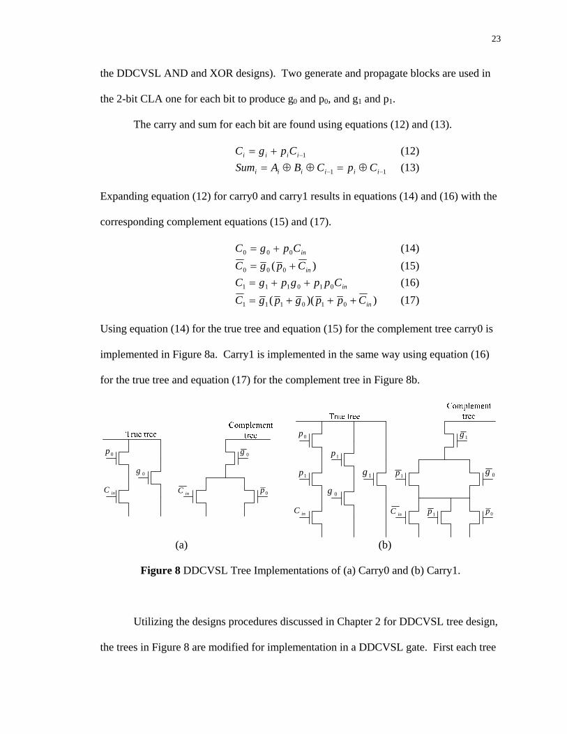
Expanding equation (12) for carry0 and carry1 results in equations (14) and (16) with the
corresponding complement equations (15) and (17).
inCpgC 000 += (14) )( 000 inCpgC += (15)
inCppgpgC 010111 ++= (16) ))(( 010111 inCppgpgC +++= (17)
Using equation (14) for the true tree and equation (15) for the complement tree carry0 is
implemented in Figure 8a. Carry1 is implemented in the same way using equation (16)
for the true tree and equation (17) for the complement tree in Figure 8b.
0p
0p
0g
0g
1g
1g1p 1p
inC inC 1p
1p0p
0p
0g
0g
inC inC
(a) (b)
Figure 8 DDCVSL Tree Implementations of (a) Carry0 and (b) Carry1.
Utilizing the designs procedures discussed in Chapter 2 for DDCVSL tree design,
the trees in Figure 8 are modified for implementation in a DDCVSL gate. First each tree
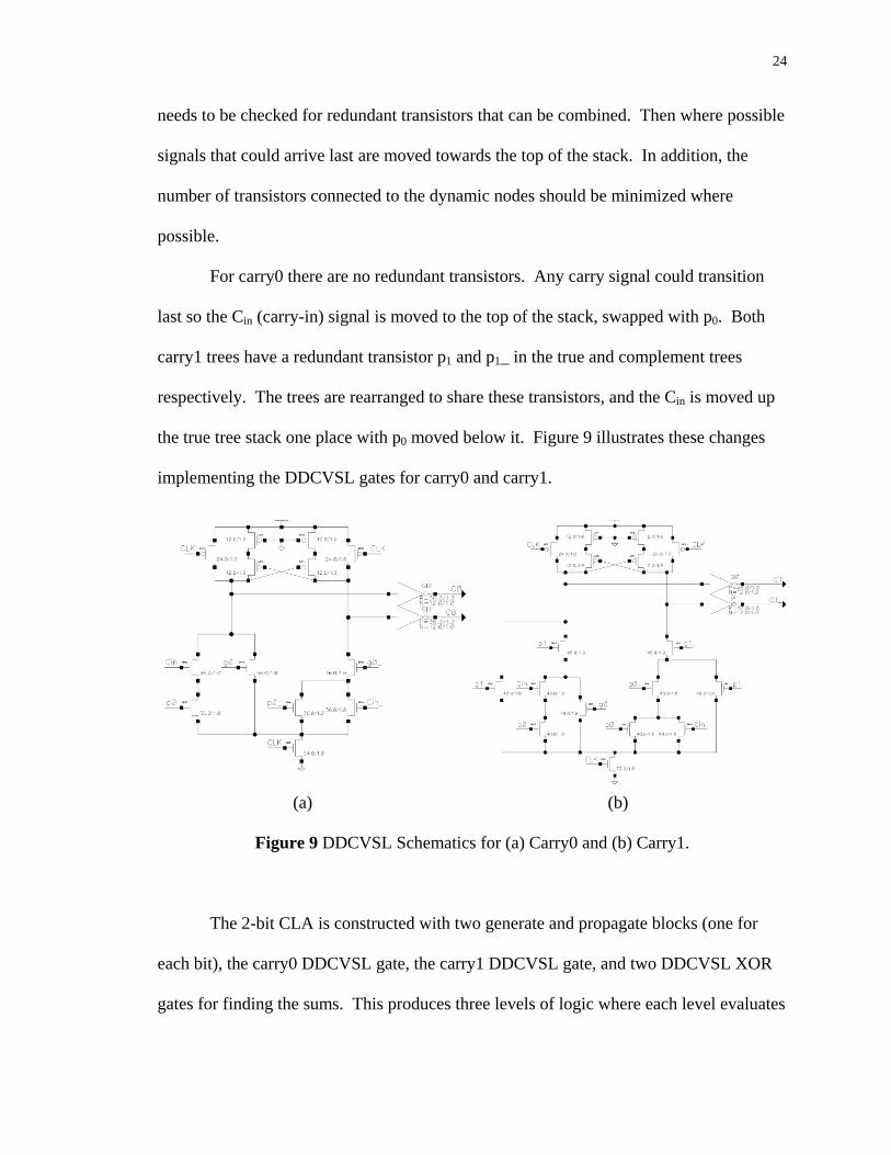
24
needs to be checked for redundant transistors that can be combined. Then where possible
signals that could arrive last are moved towards the top of the stack. In addition, the
number of transistors connected to the dynamic nodes should be minimized where
possible.
For carry0 there are no redundant transistors. Any carry signal could transition
last so the Cin (carry-in) signal is moved to the top of the stack, swapped with p0. Both
carry1 trees have a redundant transistor p1 and p1_ in the true and complement trees
respectively. The trees are rearranged to share these transistors, and the Cin is moved up
the true tree stack one place with p0 moved below it. Figure 9 illustrates these changes
implementing the DDCVSL gates for carry0 and carry1.
(a) (b)
Figure 9 DDCVSL Schematics for (a) Carry0 and (b) Carry1.
The 2-bit CLA is constructed with two generate and propagate blocks (one for
each bit), the carry0 DDCVSL gate, the carry1 DDCVSL gate, and two DDCVSL XOR
gates for finding the sums. This produces three levels of logic where each level evaluates
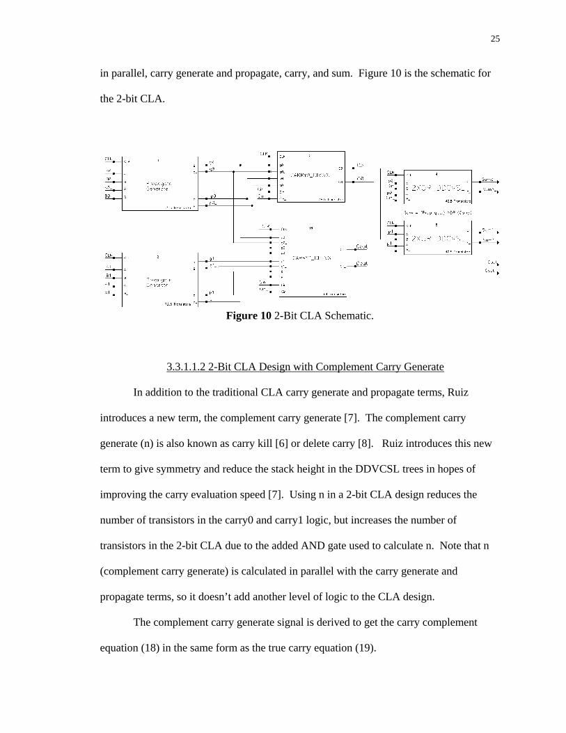
25
in parallel, carry generate and propagate, carry, and sum. Figure 10 is the schematic for
the 2-bit CLA.
Figure 10 2-Bit CLA Schematic.
3.3.1.1.2 2-Bit CLA Design with Complement Carry Generate
In addition to the traditional CLA carry generate and propagate terms, Ruiz
introduces a new term, the complement carry generate [7]. The complement carry
generate (n) is also known as carry kill [6] or delete carry [8]. Ruiz introduces this new
term to give symmetry and reduce the stack height in the DDVCSL trees in hopes of
improving the carry evaluation speed [7]. Using n in a 2-bit CLA design reduces the
number of transistors in the carry0 and carry1 logic, but increases the number of
transistors in the 2-bit CLA due to the added AND gate used to calculate n. Note that n
(complement carry generate) is calculated in parallel with the carry generate and
propagate terms, so it doesn’t add another level of logic to the CLA design.
The complement carry generate signal is derived to get the carry complement
equation (18) in the same form as the true carry equation (19).
26
)( 1−+= iiii CpgC (18)
1−+= iiii CpgC (19)
Using Boolean algebra carry complement can be written in the form of equation (20)
where the complement carry generate, n is defined by equation (21).
1−+= iiii CpnC (20)
iii pgn = (21)
Table 4 below illustrates the relationship between all three terms based on inputs A and B.
From inspection it is observed that all the terms have the mutually exclusive property [7].
Meaning that only one term is high or true for any given input combination. This is a
requirement, because these signals, carry generate, carry propagate, and complement
carry generate independent of each other define the carry bit.
Table 4 Truth Table for pi, gi, and ni [7]. Ai Bi pi gi ni
0 0 0 0 10 1 1 0 01 0 1 0 01 1 0 1 0
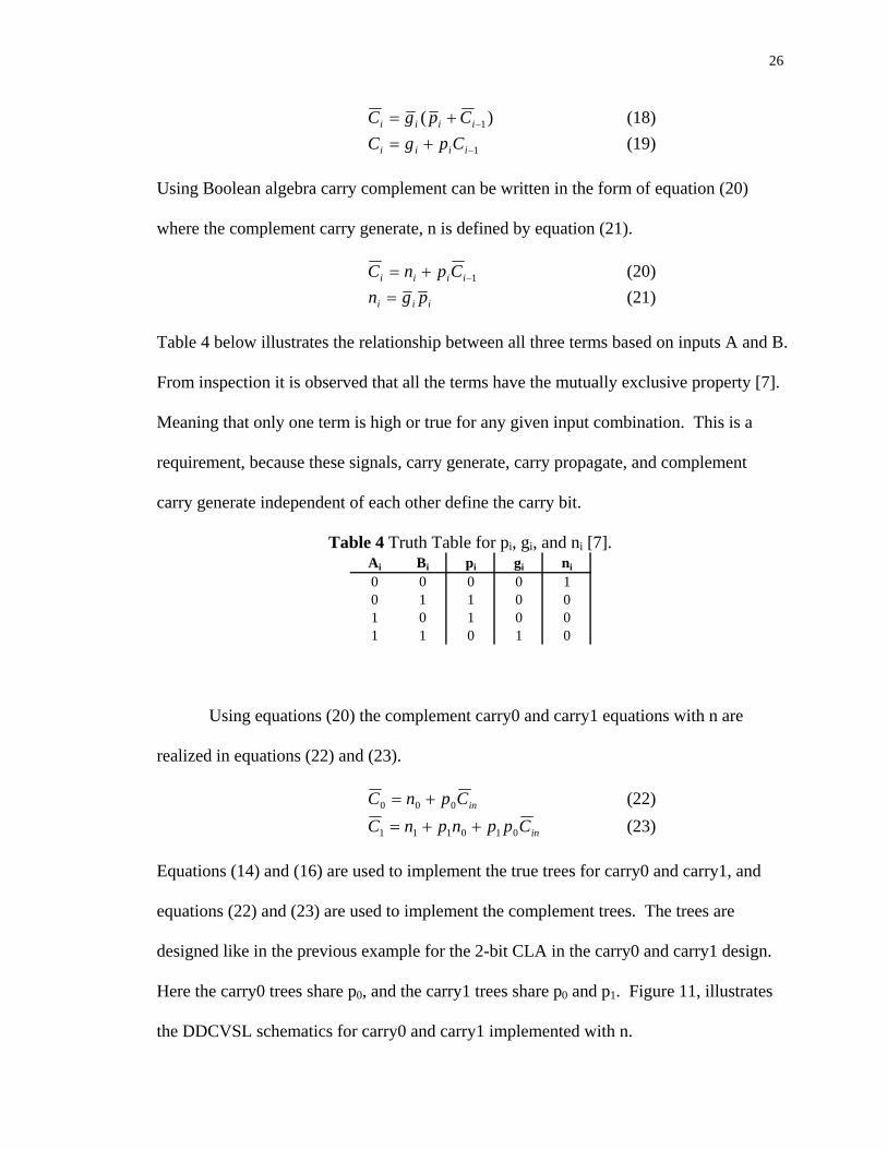
Using equations (20) the complement carry0 and carry1 equations with n are
realized in equations (22) and (23).
inCpnC 000 += (22)
inCppnpnC 010111 ++= (23)
Equations (14) and (16) are used to implement the true trees for carry0 and carry1, and
equations (22) and (23) are used to implement the complement trees. The trees are
designed like in the previous example for the 2-bit CLA in the carry0 and carry1 design.
Here the carry0 trees share p0, and the carry1 trees share p0 and p1. Figure 11, illustrates
the DDCVSL schematics for carry0 and carry1 implemented with n.
27
(a) (b)
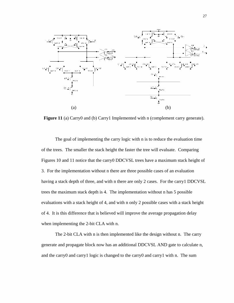
Figure 11 (a) Carry0 and (b) Carry1 Implemented with n (complement carry generate).
The goal of implementing the carry logic with n is to reduce the evaluation time
of the trees. The smaller the stack height the faster the tree will evaluate. Comparing
Figures 10 and 11 notice that the carry0 DDCVSL trees have a maximum stack height of
3. For the implementation without n there are three possible cases of an evaluation
having a stack depth of three, and with n there are only 2 cases. For the carry1 DDCVSL
trees the maximum stack depth is 4. The implementation without n has 5 possible
evaluations with a stack height of 4, and with n only 2 possible cases with a stack height
of 4. It is this difference that is believed will improve the average propagation delay
when implementing the 2-bit CLA with n.
The 2-bit CLA with n is then implemented like the design without n. The carry
generate and propagate block now has an additional DDCVSL AND gate to calculate n,
and the carry0 and carry1 logic is changed to the carry0 and carry1 with n. The sum
28
implementation remains the unchanged. The schematic is not shown here, it is basically
the same as Figure 10.
3.3.1.2 Multi-level or Treed CLA
The multi-level CLA design will also use a block size of 2 based on the
arguments presented in the single-level design. The multi-level structure attempts to
reduce the carry ripple effect evident in the single-level topology between each 2-bit
CLA structure.
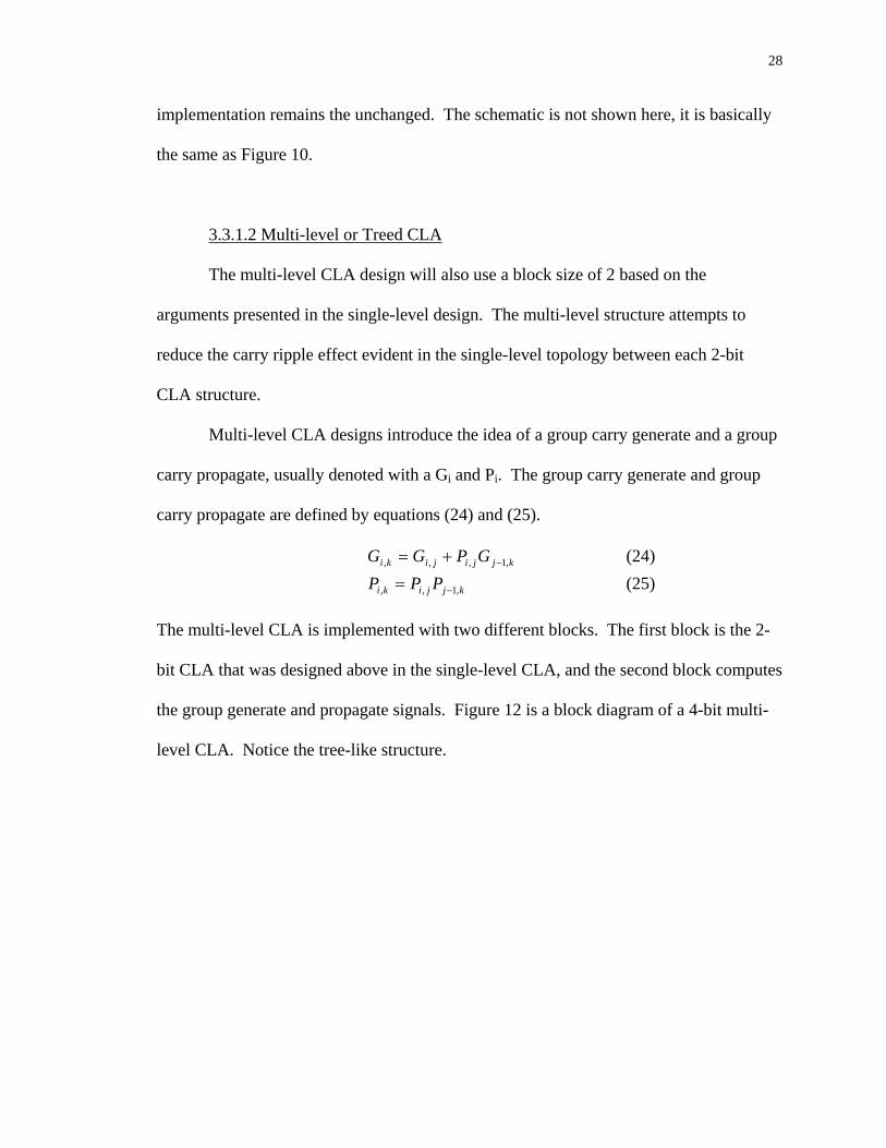
Multi-level CLA designs introduce the idea of a group carry generate and a group
carry propagate, usually denoted with a Gi and Pi. The group carry generate and group
carry propagate are defined by equations (24) and (25).
kjjijiki GPGG ,1,,, −+= (24)
kjjiki PPP ,1,, −= (25)
The multi-level CLA is implemented with two different blocks. The first block is the 2-
bit CLA that was designed above in the single-level CLA, and the second block computes
the group generate and propagate signals. Figure 12 is a block diagram of a 4-bit multi-
level CLA. Notice the tree-like structure.
29
GeneratePropagate
& SumLogic
A0 B0
Carryin
g1 p1
Sum1
GeneratePropagate
& SumLogic
A1 B1
g0 p0
Sum0
GroupGeneratePropagate
Logic
GeneratePropagate
& SumLogic
A2 B2
g3 p3
Sum3
GeneratePropagate
& SumLogic
A3 B3
g2 p2
Sum2
GroupGeneratePropagate
Logic
GroupGeneratePropagate
Logic
Carry0Carry1Carry2
GroupGeneratePropagate
Logic
Carryout
P10G10G32 P32
P30G30
Figure 12 Block Diagram of Multi-Level CLA using Group Generate and Propagate.
The first level of gates in Figure 12 is implemented with the 2-bit CLA. The rest of the
levels in the tree are then composed of the group generate and propagate blocks.
The group generate and propagate block simply implements equations (24) and
(25). The group generate equation is of the same form as the carry0 equation (14).
Group generate is then implemented with the same logic already designed for carry0 with
the inputs changed to correspond to equation (24). The group propagate equation (25), is
implemented with the DDCVSL AND gate.
30
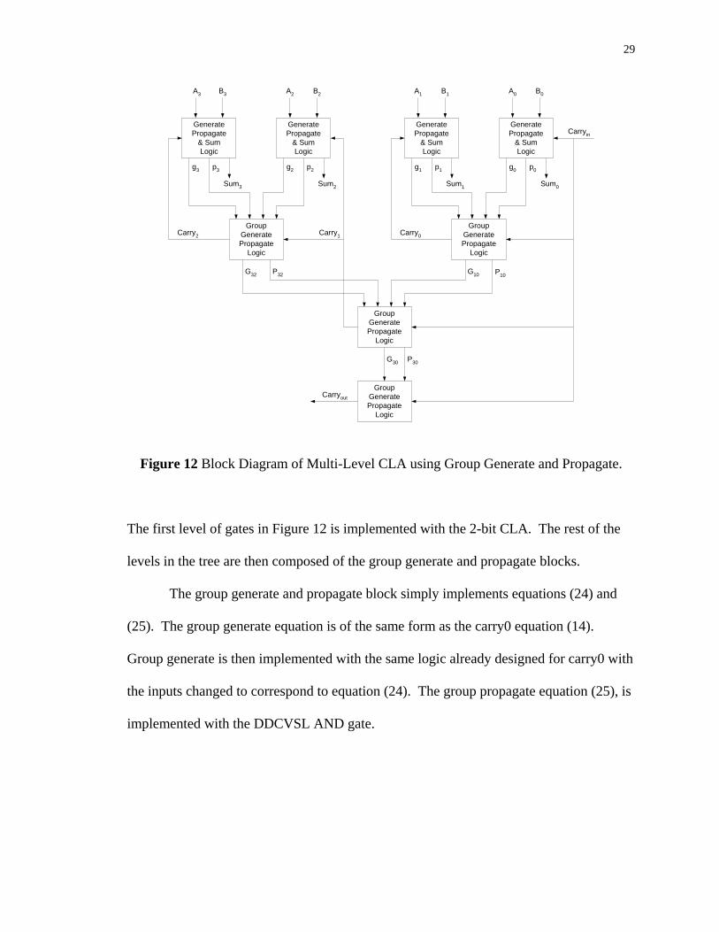
3.3.1.3 Manchester Carry Chain
The Manchester Carry Chain (MCC) is a CLA topology that uses pass-transistor
logic to propagate carrys. Ruiz suggests that the MCC is a promising dynamic CLA with
a regular, fast, and simple structure [7].
The MCC uses a series of pass-transistors to implement the carry chain. Unlike
the single-level and multi-level designs the block size of the MCC isn’t restricted by the
fan-in associated with larger block sizes for the carry signals. Ruiz suggests a block size
of four [7]. The MCC is dynamic, and all internal nodes are precharged to VDD, where
each carry has its own dynamic node. Figure 13 is the schematic for the MCC where the
carrys are implemented on the left, and the complement carrys are implemented on the
right.
Figure 13 Manchester Carry Chain Schematic [7].
Referring to the schematic the basic idea is that if any generate signal is high for
the corresponding carry it will pull the input to the skewed inverter low through the
31
evaluate transistor at the bottom of the stack. When the input of the inverter goes low
then the carry is high. If the propagate signal is high, it passes this result up the stack to
the next carry. If several of the propagate terms are high, and a lower order generate term
is high, the generate transistor may be required to pull as many as four dynamic nodes
low. This amount of load on the single generate transistor presents a sizing issue.
Higher order generate and propagate terms don’t see as much load as the lower
order terms. Rabaey suggests sizing the transistors progressively [8]. Starting at either
extreme (far left for the generates and at the top for the propagate transistors) the first
transistor is sized with the minimum sizing. Successive transistors in either the propagate
or generate chain are sized half a minimum transistor larger than the previous transistor
[8]. Like in the other DDCVSL designs the evaluate transistor at the bottom is sized 1.5
times the largest transistor.
3.3.1.4 Architecture Experiment
Three CLA topologies have been reviewed the single-level, the multi-level, and
the MCC. To determine the best CLA topology to use in the design of the 16-bit
asynchronous adder, all three are compared to find the best performance.
For the comparison the three topologies are implemented in a 4-bit configuration.
Then the time to compute the carry at the fourth bit for all possible permutations of inputs
is used to evaluate the performance. All inputs are driven with a minimum sized driver
(two inverters), and all outputs are loaded with a minimum sized inverter for simulation
purposes. Table 5 lists the average and worse case delay for each design, and the number
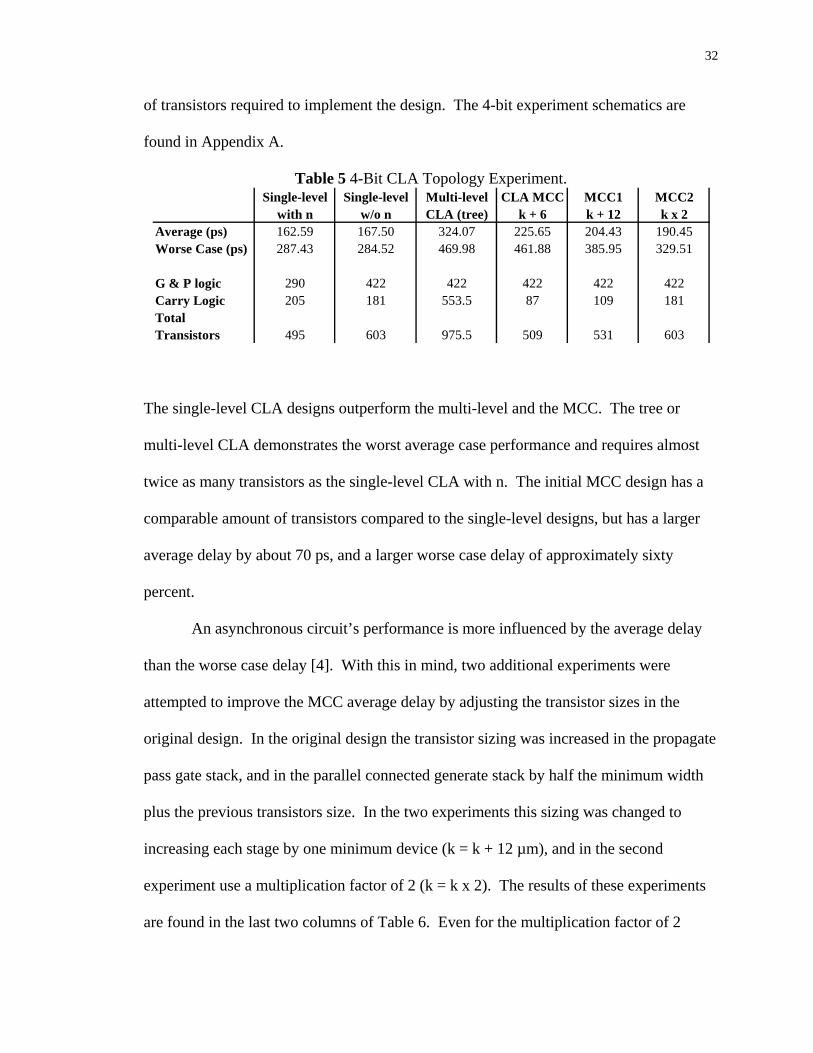
32
of transistors required to implement the design. The 4-bit experiment schematics are
found in Appendix A.
Table 5 4-Bit CLA Topology Experiment. Single-level Single-level Multi-level CLA MCC MCC1 MCC2
with n w/o n CLA (tree) k + 6 k + 12 k x 2Average (ps) 162.59 167.50 324.07 225.65 204.43 190.45Worse Case (ps) 287.43 284.52 469.98 461.88 385.95 329.51
G & P logic 290 422 422 422 422 422Carry Logic 205 181 553.5 87 109 181TotalTransistors 495 603 975.5 509 531 603
The single-level CLA designs outperform the multi-level and the MCC. The tree or
multi-level CLA demonstrates the worst average case performance and requires almost
twice as many transistors as the single-level CLA with n. The initial MCC design has a
comparable amount of transistors compared to the single-level designs, but has a larger
average delay by about 70 ps, and a larger worse case delay of approximately sixty
percent.
An asynchronous circuit’s performance is more influenced by the average delay
than the worse case delay [4]. With this in mind, two additional experiments were
attempted to improve the MCC average delay by adjusting the transistor sizes in the
original design. In the original design the transistor sizing was increased in the propagate
pass gate stack, and in the parallel connected generate stack by half the minimum width
plus the previous transistors size. In the two experiments this sizing was changed to
increasing each stage by one minimum device (k = k + 12 µm), and in the second
experiment use a multiplication factor of 2 (k = k x 2). The results of these experiments
are found in the last two columns of Table 6. Even for the multiplication factor of 2
33
sizing, the MCC average case delay is still 30 ps slower than the single-level CLA
designs.
As expected the single-level 2-bit CLA with n (complement carry generate) has a
better average case delay than the 2-bit CLA without n due to the reduced stack depth in
the DDCVSL carry logic. However, the single-level CLA without n has a better worse
case delay than the single-level CLA with n. The reason the single-level CLA design
with n has a larger worse case delay is believed to be the added input capacitance on the
dynamic node in the DDCVSL carry gates. For example, the DDCVSL carry1 gate with
n has a total of 3 transistors connected to either dynamic node compared to the DDCVSL
carry1 without n which only has 1 transistor in the complement tree and 2 transistors in
the true tree connected to the dynamic node. Based on these results the 16-bit
asynchronous adder will be designed using the single-level 2-bit CLA design with n
(complement carry generate).
3.3.2 Asynchronous Communication Design
Design of the asynchronous communication logic is critical to the asynchronous
adder performance. The asynchronous communication design includes the
communication control and the completion detection circuit. The total computation time
of the 16-bit asynchronous adder is defined by equation (26).
HSCDAddASYN tttt ++= (26)
In equation (26) tAdd is the time to complete the addition, tCD is the delay to detect
completion, and tHS is the time it takes to complete the handshaking communication with
the environment. The overhead delay associated with the asynchronous design is then tCD
34
plus tHS. If this overhead is too large the asynchronous design will not have any benefits
over the synchronous design.
3.3.2.1 Communication Control Logic
The asynchronous 16-Bit binary adder communicates with its environment in a
passive/active manner. The input and output signals used to communicate with the
environment are
Adder Inputs 1. RequestAdd – requests the adder to perform an addition. 2. AckMem – output environment acknowledges capture of the addition results. 3. AddDone – signals to the communication control that the addition is complete.
Is the output of the completion detector.
Adder Outputs 1. RequestMem – request the output environment to capture the adder results. 2. AckAdd – acknowledges to the input environment that the addition is
complete and the adder is ready for the next addition.
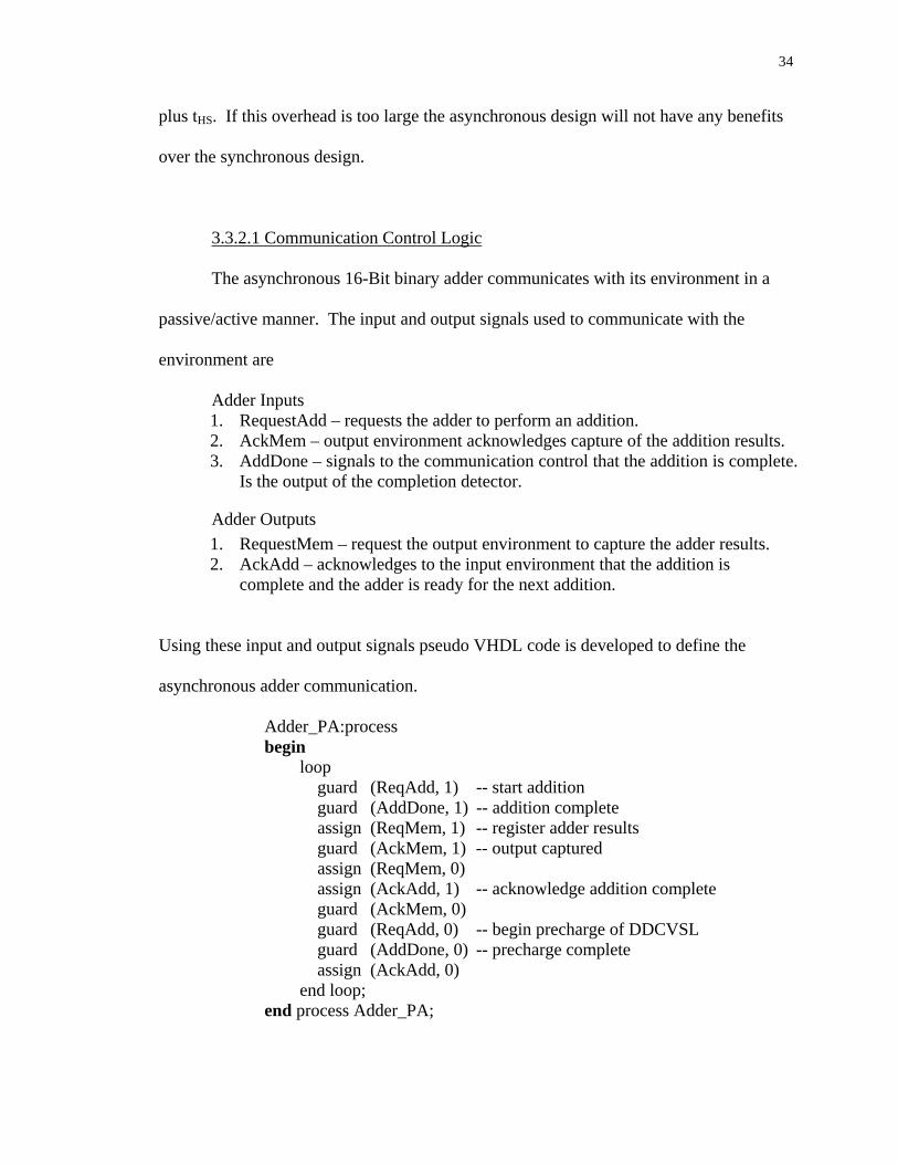
Using these input and output signals pseudo VHDL code is developed to define the
asynchronous adder communication.
Adder_PA:process begin loop
guard (ReqAdd, 1) -- start addition guard (AddDone, 1) -- addition complete assign (ReqMem, 1) -- register adder results guard (AckMem, 1) -- output captured assign (ReqMem, 0)
assign (AckAdd, 1) -- acknowledge addition complete guard (AckMem, 0) guard (ReqAdd, 0) -- begin precharge of DDCVSL guard (AddDone, 0) -- precharge complete assign (AckAdd, 0)
end loop; end process Adder_PA;
35
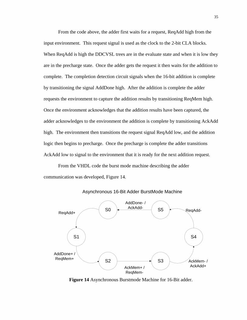
From the code above, the adder first waits for a request, ReqAdd high from the
input environment. This request signal is used as the clock to the 2-bit CLA blocks.
When ReqAdd is high the DDCVSL trees are in the evaluate state and when it is low they
are in the precharge state. Once the adder gets the request it then waits for the addition to
complete. The completion detection circuit signals when the 16-bit addition is complete
by transitioning the signal AddDone high. After the addition is complete the adder
requests the environment to capture the addition results by transitioning ReqMem high.
Once the environment acknowledges that the addition results have been captured, the
adder acknowledges to the environment the addition is complete by transitioning AckAdd
high. The environment then transitions the request signal ReqAdd low, and the addition
logic then begins to precharge. Once the precharge is complete the adder transitions
AckAdd low to signal to the environment that it is ready for the next addition request.
From the VHDL code the burst mode machine describing the adder
communication was developed, Figure 14.
S0
S1
S2 S3
S4
S5ReqAdd+
AddDone+ /ReqMem+
AckMem+ /ReqMem-
AckMem- /AckAdd+
ReqAdd-
AddDone- /AckAdd-
Asynchronous 16-Bit Adder BurstMode Machine
Figure 14 Asynchronous Burstmode Machine for 16-Bit adder.
36
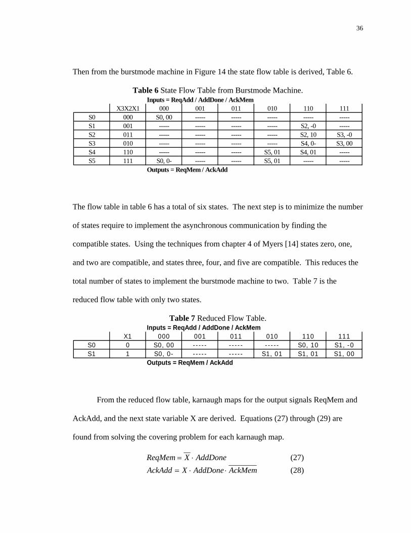
Then from the burstmode machine in Figure 14 the state flow table is derived, Table 6.
Table 6 State Flow Table from Burstmode Machine. Inputs = ReqAdd / AddDone / AckMem
X3X2X1 000 001 011 010 110 111S0 000 S0, 00 ----- ----- ----- ----- -----S1 001 ----- ----- ----- ----- S2, -0 -----S2 011 ----- ----- ----- ----- S2, 10 S3, -0S3 010 ----- ----- ----- ----- S4, 0- S3, 00S4 110 ----- ----- ----- S5, 01 S4, 01 -----S5 111 S0, 0- ----- ----- S5, 01 ----- -----
Outputs = ReqMem / AckAdd
The flow table in table 6 has a total of six states. The next step is to minimize the number
of states require to implement the asynchronous communication by finding the
compatible states. Using the techniques from chapter 4 of Myers [14] states zero, one,
and two are compatible, and states three, four, and five are compatible. This reduces the
total number of states to implement the burstmode machine to two. Table 7 is the
reduced flow table with only two states.
Table 7 Reduced Flow Table. Inputs = ReqAdd / AddDone / AckMem
X1 000 001 011 010 110 111S0 0 S0, 00 ----- ----- ----- S0, 10 S1, -0S1 1 S0, 0- ----- ----- S1, 01 S1, 01 S1, 00
Outputs = ReqMem / AckAdd
From the reduced flow table, karnaugh maps for the output signals ReqMem and
AckAdd, and the next state variable X are derived. Equations (27) through (29) are
found from solving the covering problem for each karnaugh map.
AddDoneXqMemRe ⋅= (27) AckMemAddDoneXAckAdd ⋅⋅= (28)
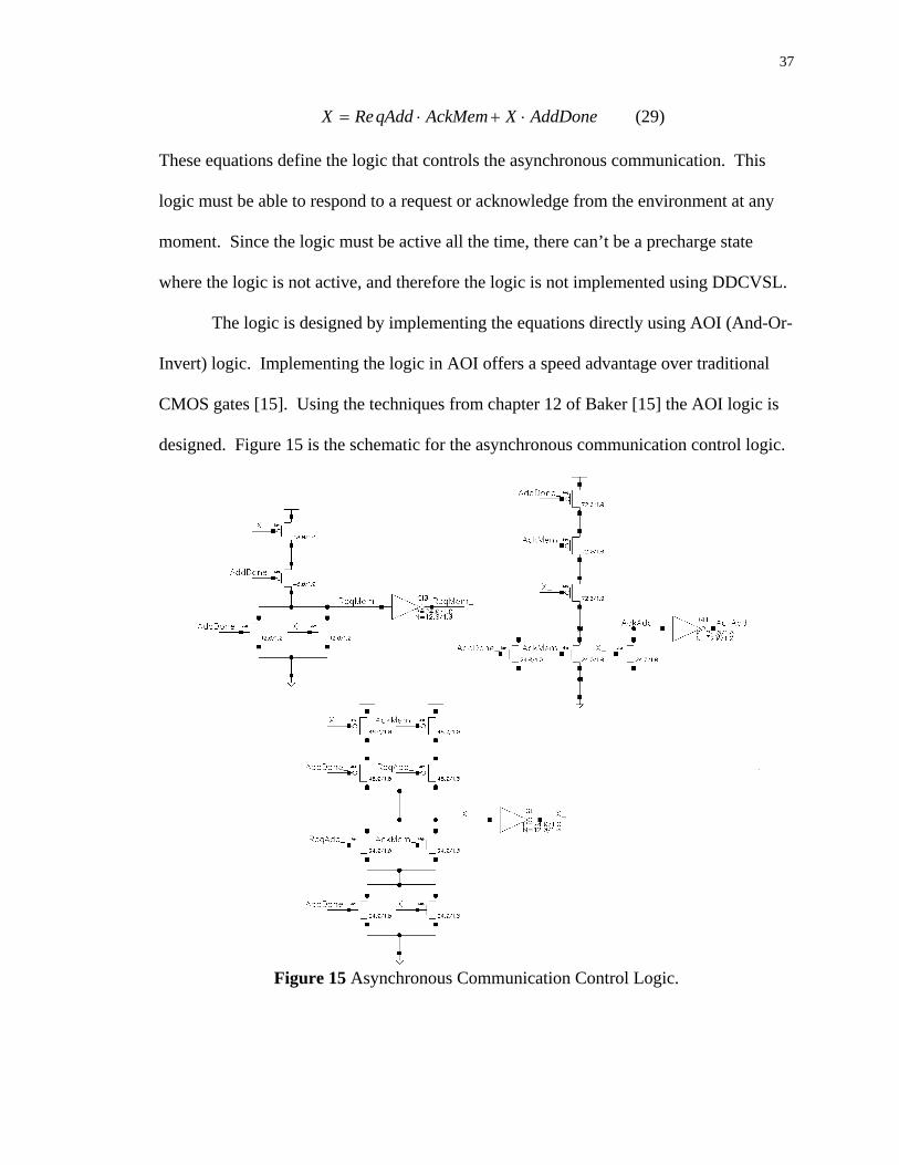
37
AddDoneXAckMemqAddReX ⋅+⋅= (29)
These equations define the logic that controls the asynchronous communication. This
logic must be able to respond to a request or acknowledge from the environment at any
moment. Since the logic must be active all the time, there can’t be a precharge state
where the logic is not active, and therefore the logic is not implemented using DDCVSL.
The logic is designed by implementing the equations directly using AOI (And-Or-
Invert) logic. Implementing the logic in AOI offers a speed advantage over traditional
CMOS gates [15]. Using the techniques from chapter 12 of Baker [15] the AOI logic is
designed. Figure 15 is the schematic for the asynchronous communication control logic.
Figure 15 Asynchronous Communication Control Logic.
38
3.3.2.2 Completion Detection Circuit
The completion detection circuit is very critical to the asynchronous adder design.
In order to achieve high performance self-timed asynchronous circuits, the key is to
design fast completion detection [16]. Its speed will inherently limit the overall
performance of the asynchronous adder. The completion detection circuit adds to the
overhead associated with an asynchronous design.
The adder is finished computing when all the sums have evaluated. Johnson
designed a completion detector that uses the carrys to detect completion rather than the
sums [1]. In a CLA architecture the carrys evaluate before the sums. Using the carrys to
detect completion allows some of the completion detection time to overlap with the sum
calculation, which masks some of the completion detection time from adding to the
overall computation time of the asynchronous adder. Johnson points out that the
asynchronous design becomes delay bounded if the completion circuit detects before the
last sum finishes evaluating [1]. The completion detection time is required to be larger
than the sum evaluation time.
The differential signaling that is used between the 2-bit CLA blocks makes it very
easy to detect completion by monitoring the differential carry signals from each 2-bit
block. When one of the differential output signals switches from the precharge state the
carry has evaluated. Figure 16a illustrates Johnson’s dynamic implementation of the
completion detection circuit using the carry signals to detect completion [1].
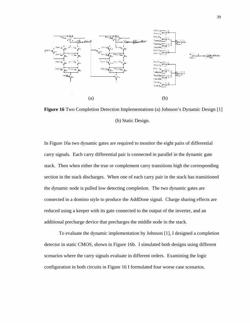
39
(a) (b)
Figure 16 Two Completion Detection Implementations (a) Johnson’s Dynamic Design [1]
(b) Static Design.
In Figure 16a two dynamic gates are required to monitor the eight pairs of differential
carry signals. Each carry differential pair is connected in parallel in the dynamic gate
stack. Then when either the true or complement carry transitions high the corresponding
section in the stack discharges. When one of each carry pair in the stack has transitioned
the dynamic node is pulled low detecting completion. The two dynamic gates are
connected in a domino style to produce the AddDone signal. Charge sharing effects are
reduced using a keeper with its gate connected to the output of the inverter, and an
additional precharge device that precharges the middle node in the stack.
To evaluate the dynamic implementation by Johnson [1], I designed a completion
detector in static CMOS, shown in Figure 16b. I simulated both designs using different
scenarios where the carry signals evaluate in different orders. Examining the logic
configuration in both circuits in Figure 16 I formulated four worse case scenarios.
40
Test Sets 1. Each carry evaluates in succession. 2. Carry3 evaluates last (dynamic worse case) 3. Carry7 evaluates last (dynamic & static) 4. Carry5 evaluates last (a static worse case)
Test set 1 is tested, because it is associated with the worse case delay of the adder where
the carry-in is propagated through the entire adder. The remaining test sets are developed
based on transistor placement.
When using large stacks of transistors a worse case delay occurs when the bottom
transistor in the stack evaluates last. This is due to the smaller VDS across the bottom
transistor. Carry1 is the input to the bottom transistor in the first dynamic gate stack in
Figure 16a. However, the Carry1 evaluation time is not dependent on the previous blocks
addition time. Therefore, Carry1 will never take longer than any other carry to evaluate.
Carry3, the input to the second transistor from the bottom of the stack could evaluate
after all other carrys. This is the worse case scenario for the dynamic completion detector
and is used for test set 2. Test set 3 is from a possible worse case evaluation in the static
CMOS implementation in Figure 16b. In the static design the Carry7 and Carry7_ result
from the 2-input NAND gate is connected to the bottom transistor in a 4-input NAND
gate. Test set 4 uses Carry5 evaluating last, which is a possible secondary worse case in
each design.
The simulation results of these test sets resulted in the Johnson’s dynamic
implementation only outperforming the static case for test set 1. The static design
outperforming the dynamic design for any test condition was unexpected. Examining the
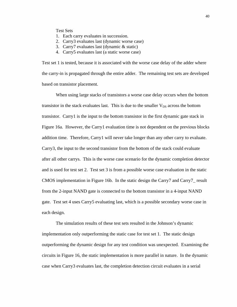
circuits in Figure 16, the static implementation is more parallel in nature. In the dynamic
case when Carry3 evaluates last, the completion detection circuit evaluates in a serial
41
manner. In addition, the dynamic circuit has 5 levels of logic and the static has 4 levels
of logic. The dynamic completion detector is modified to reduce the number of logic
levels and introduce a more parallel structure, Figure 17.
Figure 17 Dynamic Completion Detector with Parallel Structure.
In Figure 17 the dynamic gates are connected in parallel rather than in series using
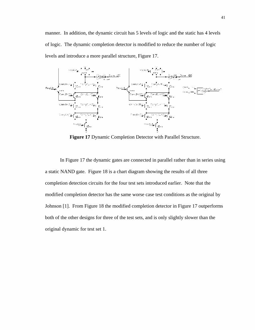
a static NAND gate. Figure 18 is a chart diagram showing the results of all three
completion detection circuits for the four test sets introduced earlier. Note that the
modified completion detector has the same worse case test conditions as the original by
Johnson [1]. From Figure 18 the modified completion detector in Figure 17 outperforms
both of the other designs for three of the test sets, and is only slightly slower than the
original dynamic for test set 1.
42
Completion Detection Circuit Comparison
0.00
50.00
100.00
150.00
200.00
250.00
300.00
350.00
DataSet0 DataSet1 DataSet2 DataSet3
Del
ay (p
s) Dynamic
Static
Mod.Dynamic
Figure 18 Results of Three Completion Detection Circuits using Four Test Conditions.
One of the requirements of the completion detector using the carry signals to
detect completion was that it must have a longer evaluation time then the slowest sum
evaluation. From Figure 18 the fastest completion detection time is 93 ps for test set 1.
The sums in the adder are implemented using the DDCVSL XOR gates. From Table 3
the longest DDCVSL XOR evaluation is 87 ps, which barely meets the requirement. The
delay associated with the communication control logic provides additional margin to this
timing requirement. Then the modified completion detector can be used in the
asynchronous 16-bit adder design where most of the completion detection time is
concealed during the sum evaluation.
3.3.3 Asynchronous16-Bit Adder
The asynchronous adder design is composed of 2-bit CLA blocks, a completion
detector, and asynchronous communication logic. From the architecture experiment, the
43
2-bit CLA with n was selected for implementing the 16-bit adder. Eight 2-bit CLA
blocks are then cascaded in a single-level to form the full 16-bits. The asynchronous
communication logic handles the handshaking between the input and output environment.
The completion detector informs the asynchronous communication logic when an
addition is complete. The ReqAdd input to the adder is used in the asynchronous logic to
determine the state of the adder, and is also used as the clock to the 2-bit CLA blocks.
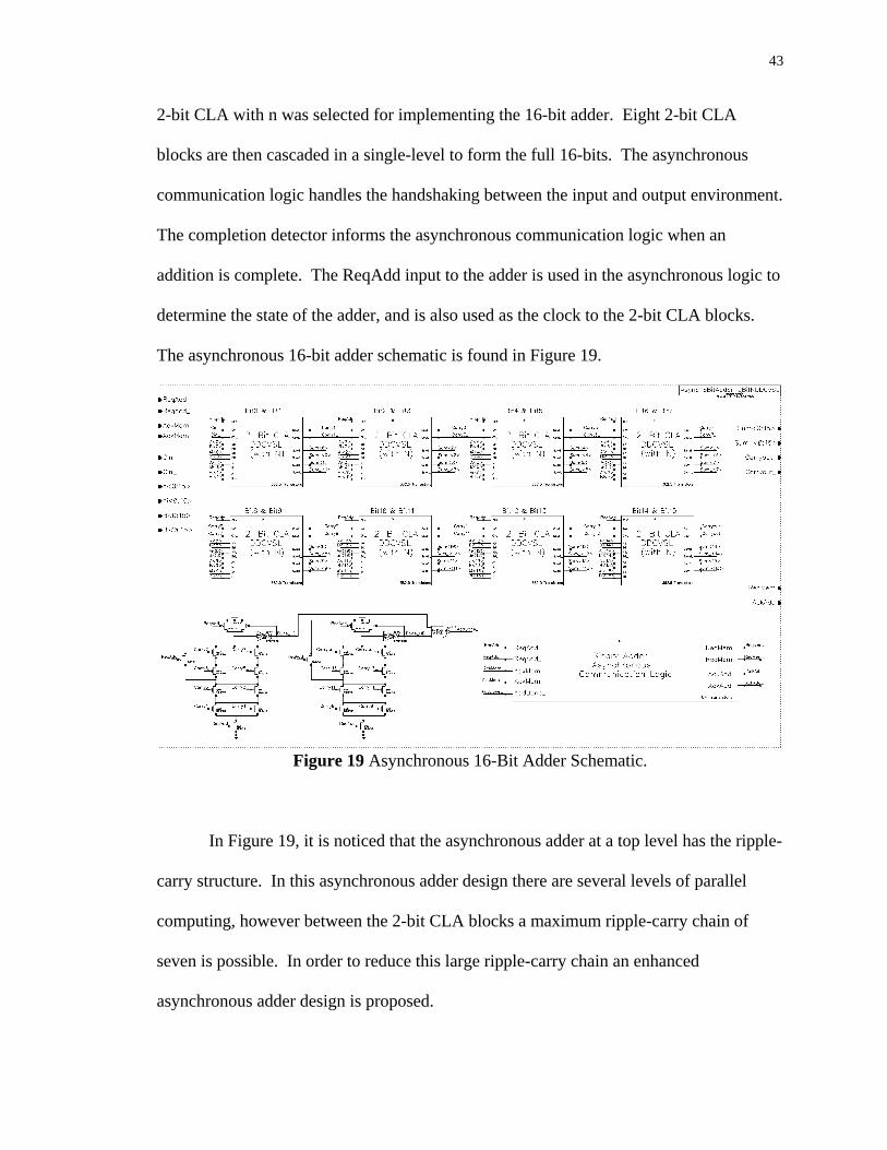
The asynchronous 16-bit adder schematic is found in Figure 19.
Figure 19 Asynchronous 16-Bit Adder Schematic.
In Figure 19, it is noticed that the asynchronous adder at a top level has the ripple-
carry structure. In this asynchronous adder design there are several levels of parallel
computing, however between the 2-bit CLA blocks a maximum ripple-carry chain of
seven is possible. In order to reduce this large ripple-carry chain an enhanced
asynchronous adder design is proposed.
44
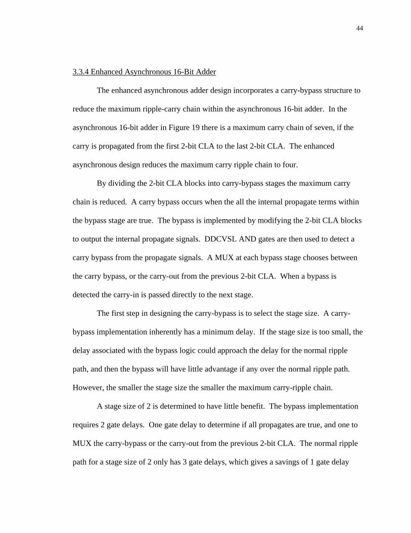
3.3.4 Enhanced Asynchronous 16-Bit Adder
The enhanced asynchronous adder design incorporates a carry-bypass structure to
reduce the maximum ripple-carry chain within the asynchronous 16-bit adder. In the
asynchronous 16-bit adder in Figure 19 there is a maximum carry chain of seven, if the
carry is propagated from the first 2-bit CLA to the last 2-bit CLA. The enhanced
asynchronous design reduces the maximum carry ripple chain to four.
By dividing the 2-bit CLA blocks into carry-bypass stages the maximum carry
chain is reduced. A carry bypass occurs when the all the internal propagate terms within
the bypass stage are true. The bypass is implemented by modifying the 2-bit CLA blocks
to output the internal propagate signals. DDCVSL AND gates are then used to detect a
carry bypass from the propagate signals. A MUX at each bypass stage chooses between
the carry bypass, or the carry-out from the previous 2-bit CLA. When a bypass is
detected the carry-in is passed directly to the next stage.
The first step in designing the carry-bypass is to select the stage size. A carry-
bypass implementation inherently has a minimum delay. If the stage size is too small, the
delay associated with the bypass logic could approach the delay for the normal ripple
path, and then the bypass will have little advantage if any over the normal ripple path.
However, the smaller the stage size the smaller the maximum carry-ripple chain.
A stage size of 2 is determined to have little benefit. The bypass implementation
requires 2 gate delays. One gate delay to determine if all propagates are true, and one to
MUX the carry-bypass or the carry-out from the previous 2-bit CLA. The normal ripple
path for a stage size of 2 only has 3 gate delays, which gives a savings of 1 gate delay
45
when the bypass is used. A stage size of 4 on the other hand has a carry-ripple of 5 gate
delays, and with the carry bypass would give a savings of 3 gate delays.
With a bypass stage size of 4 every 2-bit CLA block after the fourth has a carry-
bypass path. Figure 20 is the schematic for the enhanced asynchronous 16-bit adder with
a reduced maximum carry chain of four.
Figure 20 Enhanced Asynchronous 16-Bit Adder with Carry-Bypass.
3.4 Synchronous Adder Design
The synchronous 16-bit adder design involves selecting the best architecture for a
synchronous implementation, and designing the logic. The synchronous adder will
operate at a frequency equal to its worse case computation time. It is therefore critical to
reduce the worse case computation in the synchronous design.
46
3.4.1 Architecture
The synchronous adder is synchronized at a constant clock rate. Since the input
data is unknown, this clock rate must be set to handle the worse case data-dependent
computation delay. For high-speed performance the synchronous architecture is then
selected based on the best worse case delay, rather than the best average delay like the
asynchronous design.
The Carry-Select Adder (CSA) architecture is considered one of the fastest adder
architectures, especially for a synchronous implementation [4]. This architecture
computes the carry-out and sums based on both possible values of carry-in. Then once
the carry-in arrives the correct sum and carry-out are chosen from a MUX.
For the worse case computation the CSA is the fastest adder architecture for two
reasons. First the data dependence is virtually nonexistent since the adder computes both
sets of results for the two possible carry-in values. Second the computation delay
dependence on the number of bits implemented in the adder is reduced compared to other
architectures. The computation time of this architecture only increases by a MUX delay
for each additional bit in the architecture. See Chapter 2 section 2.2 for a more detailed
explanation of the CSA.
3.4.2 Carry-Select Adder Design
The CSA architecture is used to implement the synchronous 16-bit adder. The
CSA architecture like the CLA in the asynchronous design is implemented with blocks to
construct the full 16-bit adder. The larger the CSA block size the more carry dependent
delay occurs within the block. As the block size is decreased the total MUX delay
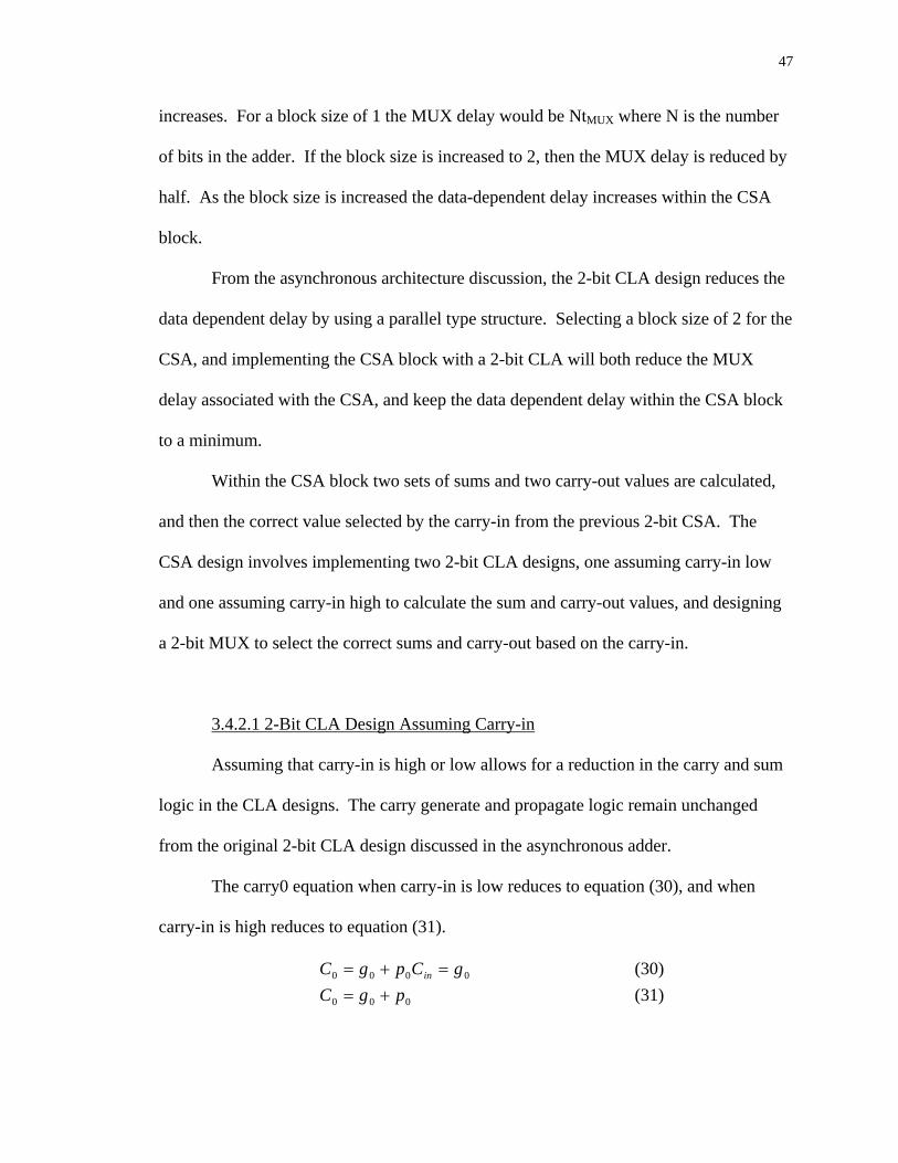
47
increases. For a block size of 1 the MUX delay would be NtMUX where N is the number
of bits in the adder. If the block size is increased to 2, then the MUX delay is reduced by
half. As the block size is increased the data-dependent delay increases within the CSA
block.
From the asynchronous architecture discussion, the 2-bit CLA design reduces the
data dependent delay by using a parallel type structure. Selecting a block size of 2 for the
CSA, and implementing the CSA block with a 2-bit CLA will both reduce the MUX
delay associated with the CSA, and keep the data dependent delay within the CSA block
to a minimum.
Within the CSA block two sets of sums and two carry-out values are calculated,
and then the correct value selected by the carry-in from the previous 2-bit CSA. The
CSA design involves implementing two 2-bit CLA designs, one assuming carry-in low
and one assuming carry-in high to calculate the sum and carry-out values, and designing
a 2-bit MUX to select the correct sums and carry-out based on the carry-in.
3.4.2.1 2-Bit CLA Design Assuming Carry-in
Assuming that carry-in is high or low allows for a reduction in the carry and sum
logic in the CLA designs. The carry generate and propagate logic remain unchanged
from the original 2-bit CLA design discussed in the asynchronous adder.
The carry0 equation when carry-in is low reduces to equation (30), and when
carry-in is high reduces to equation (31).
0000 gCpgC in =+= (30)
000 pgC += (31)
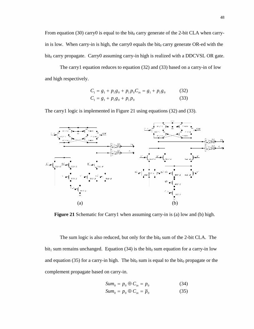
48
From equation (30) carry0 is equal to the bit0 carry generate of the 2-bit CLA when carry-
in is low. When carry-in is high, the carry0 equals the bit0 carry generate OR-ed with the
bit0 carry propagate. Carry0 assuming carry-in high is realized with a DDCVSL OR gate.
The carry1 equation reduces to equation (32) and (33) based on a carry-in of low
and high respectively.
011010111 gpgCppgpgC in +=++= (32)
010111 ppgpgC ++= (33)
The carry1 logic is implemented in Figure 21 using equations (32) and (33).
(a) (b)
Figure 21 Schematic for Carry1 when assuming carry-in is (a) low and (b) high.
The sum logic is also reduced, but only for the bit0 sum of the 2-bit CLA. The
bit1 sum remains unchanged. Equation (34) is the bit0 sum equation for a carry-in low
and equation (35) for a carry-in high. The bit0 sum is equal to the bit0 propagate or the
complement propagate based on carry-in.
000 pCpSum in =⊕= (34)
000 pCpSum in =⊕= (35)
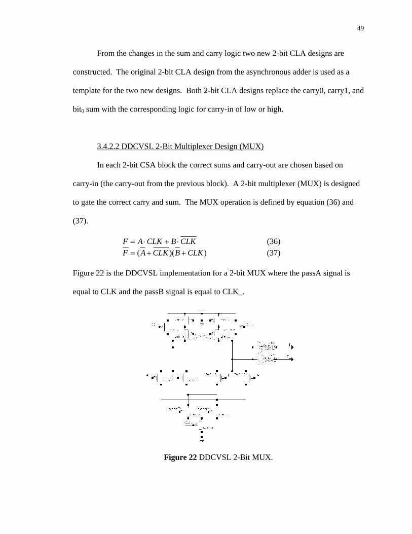
49
From the changes in the sum and carry logic two new 2-bit CLA designs are
constructed. The original 2-bit CLA design from the asynchronous adder is used as a
template for the two new designs. Both 2-bit CLA designs replace the carry0, carry1, and
bit0 sum with the corresponding logic for carry-in of low or high.
3.4.2.2 DDCVSL 2-Bit Multiplexer Design (MUX)
In each 2-bit CSA block the correct sums and carry-out are chosen based on
carry-in (the carry-out from the previous block). A 2-bit multiplexer (MUX) is designed
to gate the correct carry and sum. The MUX operation is defined by equation (36) and
(37).
CLKBCLKAF ⋅+⋅= (36) ))(( CLKBCLKAF ++= (37)
Figure 22 is the DDCVSL implementation for a 2-bit MUX where the passA signal is
equal to CLK and the passB signal is equal to CLK_.
Figure 22 DDCVSL 2-Bit MUX.
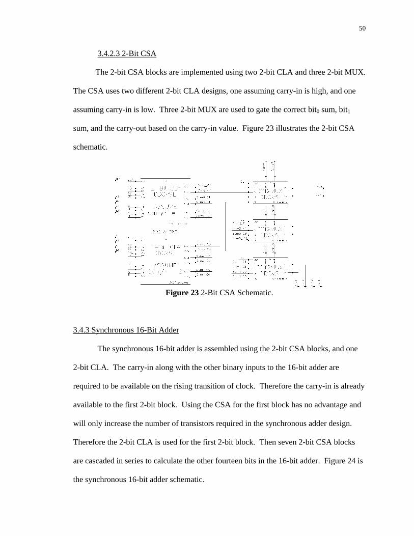
50
3.4.2.3 2-Bit CSA
The 2-bit CSA blocks are implemented using two 2-bit CLA and three 2-bit MUX.
The CSA uses two different 2-bit CLA designs, one assuming carry-in is high, and one
assuming carry-in is low. Three 2-bit MUX are used to gate the correct bit0 sum, bit1
sum, and the carry-out based on the carry-in value. Figure 23 illustrates the 2-bit CSA
schematic.
Figure 23 2-Bit CSA Schematic.
3.4.3 Synchronous 16-Bit Adder
The synchronous 16-bit adder is assembled using the 2-bit CSA blocks, and one
2-bit CLA. The carry-in along with the other binary inputs to the 16-bit adder are
required to be available on the rising transition of clock. Therefore the carry-in is already
available to the first 2-bit block. Using the CSA for the first block has no advantage and
will only increase the number of transistors required in the synchronous adder design.
Therefore the 2-bit CLA is used for the first 2-bit block. Then seven 2-bit CSA blocks
are cascaded in series to calculate the other fourteen bits in the 16-bit adder. Figure 24 is
the synchronous 16-bit adder schematic.
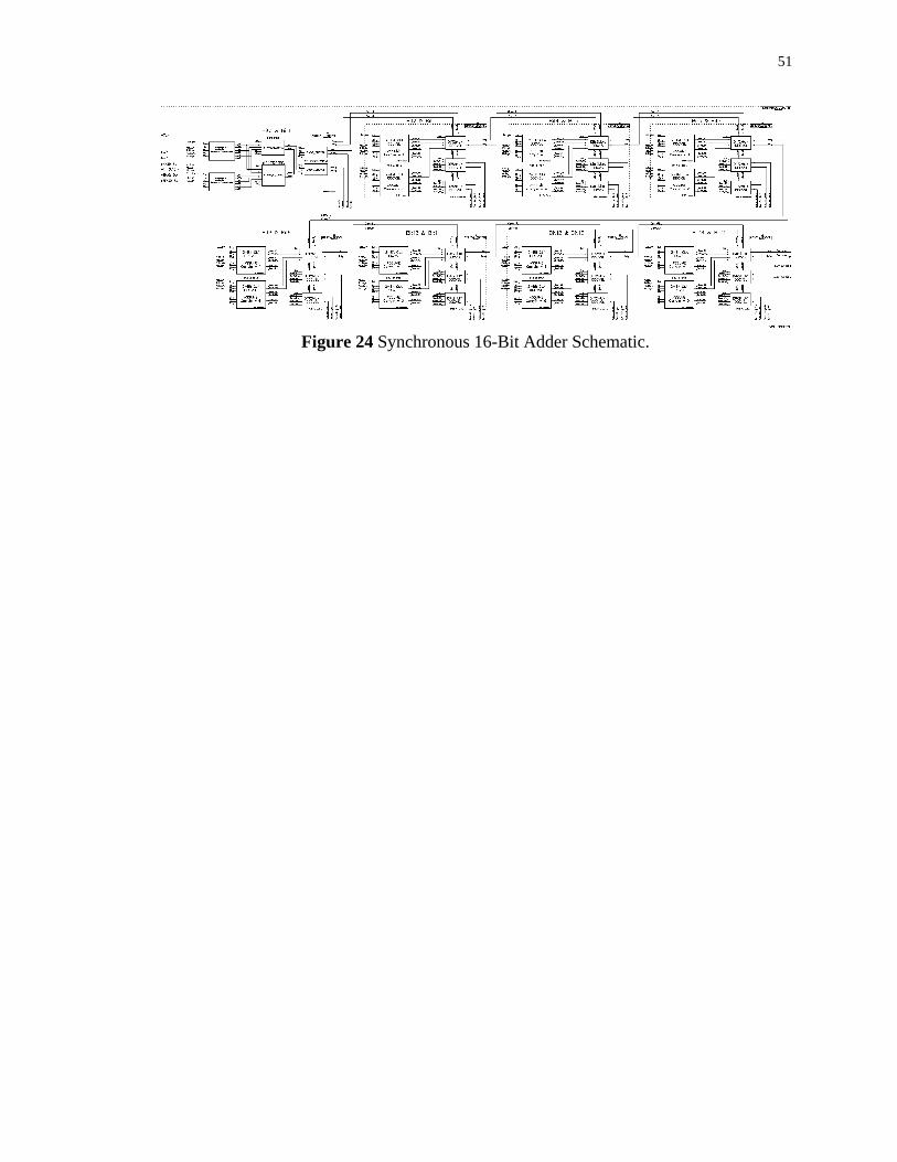
51
Figure 24 Synchronous 16-Bit Adder Schematic.
52
CHAPTER 4 - SIMULATION RESULTS
Simulations are run to verify the adder designs for correct operation, and to
evaluate the performance of each design. The synchronous adder will operate at the same
speed for all input conditions, which is defined by the worse case computation delay.
The asynchronous adder operates at a rate that is data-dependent. The asynchronous and
synchronous designs are evaluated using two different comparisons. First the
synchronous operating frequency is compared to the asynchronous adder’s performance
for 10,000 random test vectors. For the second experiment the adders are implemented
into an adder system and 32 consecutive additions are performed.
4.1 Test Vector Generation Using A PERL Program
To verify the designs, find the worse case delay, and find the average delay based
on 10,000 random inputs, requires a large number of input voltage sources with each
source having multiple transitions. Determining these transitions and manually
generating the sources in a flat text file is an unreasonable and a time-consuming task,
especially for the 10,000 random inputs. To accomplish this task a PERL program was
written to generate the multiple voltage sources. The sources can be generated based on
all possible permutations or on random data. The program specifies each source and its
corresponding value over time in a piece-wise linear voltage source statement. As the
program was developed additional features were discovered and implemented. Using this
PERL program made the testing and verification of the adder designs straightforward and
convenient. Appendix B lists the PERL code for the generateSource program.

53
The generateSource PERL program prompts the user for the following information.
1. Test vectors generated based on random or all possible permutations. 2. Template source name (sourcename = template + current source number). 3. Number of voltage sources. 4. Number of data vectors. If all permutations, number of data vectors is based
on number of sources 2N where N is the number of sources. 5. Data cycle time, time between each test vector. 6. Rise and fall time of each input source. 7. Generate differential sources. 8. Generate source results files based on binary addition of voltage sources. 9. Generate delay measurement file.
The generateSource program first prompts the user whether to generate random data or
all possible permutations. Then the program asks the user to input the default or template
name for the voltage sources, and the number of sources to generate. Each source is
generated in a separate file with a filename that corresponds to the source name. The
filename includes the template voltage source name and a number based on the total
number of sources. If random test vectors are generated the user is asked how many
random vectors to generate. If all permutations are generated the program generates 2N
permutations where N is the number of input sources to generate. Once the data values
are known, the program also needs to know the data cycle time, and the rise and fall time
for each transition to create the piece-wise linear voltage sources. Since the adder
designs require differential inputs the program then offers to generate differential sources.
The program writes all the sources to their corresponding files. To use these voltage
sources in a simulation the source filenames are included in the simulation control file.
The generateSource program generates the input voltage sources that specify the
binary numbers that are added by the adders. Since the program has the addition
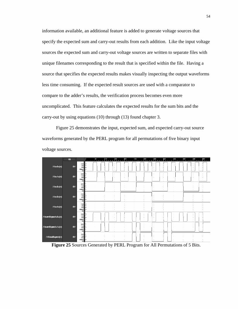
54
information available, an additional feature is added to generate voltage sources that
specify the expected sum and carry-out results from each addition. Like the input voltage
sources the expected sum and carry-out voltage sources are written to separate files with
unique filenames corresponding to the result that is specified within the file. Having a
source that specifies the expected results makes visually inspecting the output waveforms
less time consuming. If the expected result sources are used with a comparator to
compare to the adder’s results, the verification process becomes even more
uncomplicated. This feature calculates the expected results for the sum bits and the
carry-out by using equations (10) through (13) found chapter 3.
Figure 25 demonstrates the input, expected sum, and expected carry-out source
waveforms generated by the PERL program for all permutations of five binary input
voltage sources.
Figure 25 Sources Generated by PERL Program for All Permutations of 5 Bits.
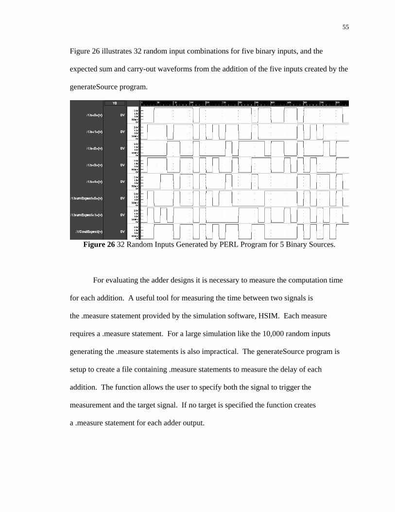
55
Figure 26 illustrates 32 random input combinations for five binary inputs, and the
expected sum and carry-out waveforms from the addition of the five inputs created by the
generateSource program.
Figure 26 32 Random Inputs Generated by PERL Program for 5 Binary Sources.
For evaluating the adder designs it is necessary to measure the computation time
for each addition. A useful tool for measuring the time between two signals is
the .measure statement provided by the simulation software, HSIM. Each measure
requires a .measure statement. For a large simulation like the 10,000 random inputs
generating the .measure statements is also impractical. The generateSource program is
setup to create a file containing .measure statements to measure the delay of each
addition. The function allows the user to specify both the signal to trigger the
measurement and the target signal. If no target is specified the function creates
a .measure statement for each adder output.
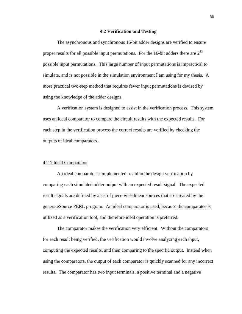
56
4.2 Verification and Testing
The asynchronous and synchronous 16-bit adder designs are verified to ensure
proper results for all possible input permutations. For the 16-bit adders there are 233
possible input permutations. This large number of input permutations is impractical to
simulate, and is not possible in the simulation environment I am using for my thesis. A
more practical two-step method that requires fewer input permutations is devised by
using the knowledge of the adder designs.
A verification system is designed to assist in the verification process. This system
uses an ideal comparator to compare the circuit results with the expected results. For
each step in the verification process the correct results are verified by checking the
outputs of ideal comparators.
4.2.1 Ideal Comparator
An ideal comparator is implemented to aid in the design verification by
comparing each simulated adder output with an expected result signal. The expected
result signals are defined by a set of piece-wise linear sources that are created by the
generateSource PERL program. An ideal comparator is used, because the comparator is
utilized as a verification tool, and therefore ideal operation is preferred.
The comparator makes the verification very efficient. Without the comparators
for each result being verified, the verification would involve analyzing each input,
computing the expected results, and then comparing to the specific output. Instead when
using the comparators, the output of each comparator is quickly scanned for any incorrect
results. The comparator has two input terminals, a positive terminal and a negative
57
terminal. If both terminals are equal, then the comparator’s output is 0 volts. If the
positive terminal is at a higher voltage than the negative terminal, then the output of the
comparator is VDD, and if the negative terminal is at a higher voltage than the positive
terminal the output is –VDD. Figure 27 illustrates the comparator operation for passing
and failing cases.
Figure 27 Verification Results Using An Ideal Comparator.
To demonstrate the comparators operation, the expected result sources
SumExpect<0> and SumExpect<1> were modified with incorrect results. In Figure 27
the comparator output signals are Sum0result, Sum1result, and Carryresult. Both the
Sum0result and Sum1result signals transition above and below the zero level indicating
that the comparators detected the incorrect results that were modified. The Carryresult
signal maintains a zero level throughout all the test vectors indicating the carry was
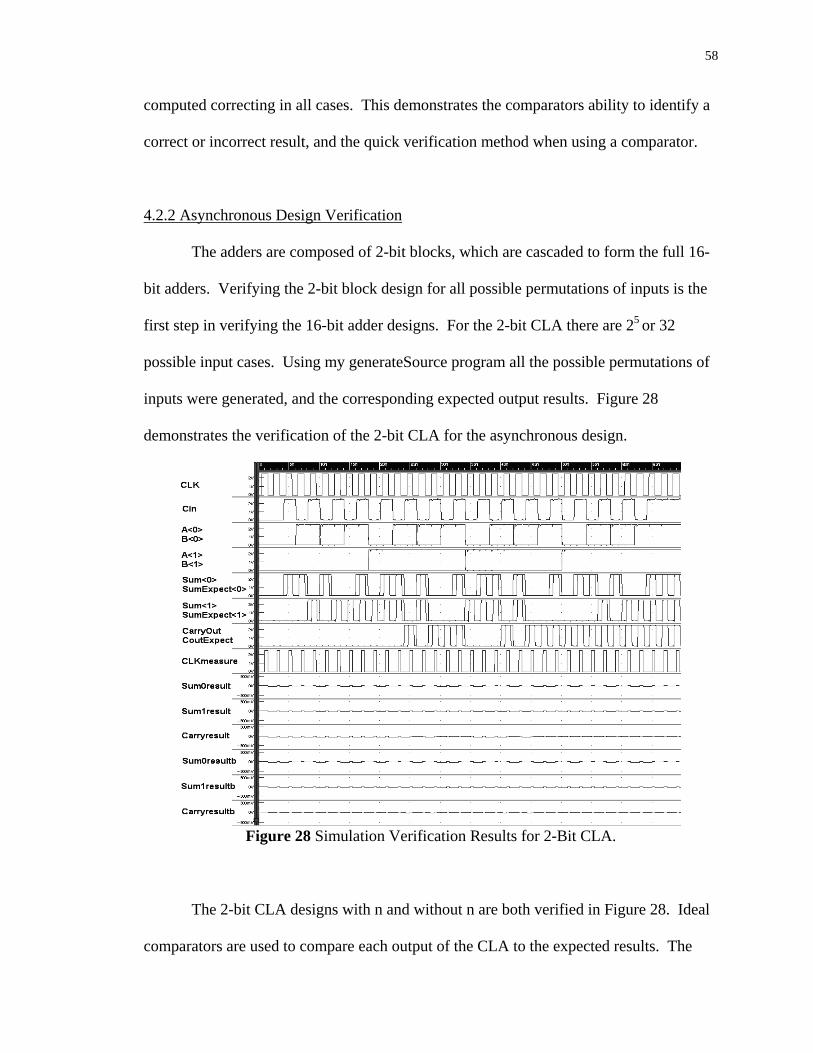
58
computed correcting in all cases. This demonstrates the comparators ability to identify a
correct or incorrect result, and the quick verification method when using a comparator.
4.2.2 Asynchronous Design Verification
The adders are composed of 2-bit blocks, which are cascaded to form the full 16-
bit adders. Verifying the 2-bit block design for all possible permutations of inputs is the
first step in verifying the 16-bit adder designs. For the 2-bit CLA there are 25 or 32
possible input cases. Using my generateSource program all the possible permutations of
inputs were generated, and the corresponding expected output results. Figure 28
demonstrates the verification of the 2-bit CLA for the asynchronous design.
Figure 28 Simulation Verification Results for 2-Bit CLA.
The 2-bit CLA designs with n and without n are both verified in Figure 28. Ideal
comparators are used to compare each output of the CLA to the expected results. The
59
Sum0result, Sum1result, and Carryresult are the output of the comparators for the 2-bit
CLA without n. In Figure 28 these signals maintain a zero level throughout all input
permutations verifying the 2-bit CLA without n design. The Sum0resultb, Sum1resultb,
and Carryresultb are the output of the comparators for the 2-bit CLA with n. Again in
figure 24 these signals maintain a zero level verifying the 2-bit CLA with n design.
If the 2-bit CLA blocks are verified, then it follows that once their interconnection
is confirmed within the 16-bit adder, the full 16-bit design is then verified. The 2-bit
CLA blocks within the 16-bit adder are connected by carry signals. By propagating a
carry from the first 2-bit CLA to the last 2-bit CLA will verify this interconnection. This
was accomplished by setting the 16-bit adder carry-in value to high, setting all the bits of
the binary number A high, and all the bits of the binary number B low, where the adder is
adding A and B. By setting the bits of A high, and the bits of B low a carry propagate is
created at each bit position within the adder, and the original carry-in high is propagated
through all 2-bit CLA to the carry-out of the adder. This input condition was applied to
the asynchronous 16-bit adder design and the correct result verified. Therefore the
asynchronous 16-bit adder is verified for correct operation for all possible input values.
4.2.3 Synchronous Design Verification
The synchronous design is composed of 2-bit CSA blocks to form the full 16-bit
adder. Like the asynchronous design verification, the first step in verifying the
synchronous design is to verify these 2-bit blocks. Figure 29 illustrates the verification of
the 2-bit CSA for the synchronous design.
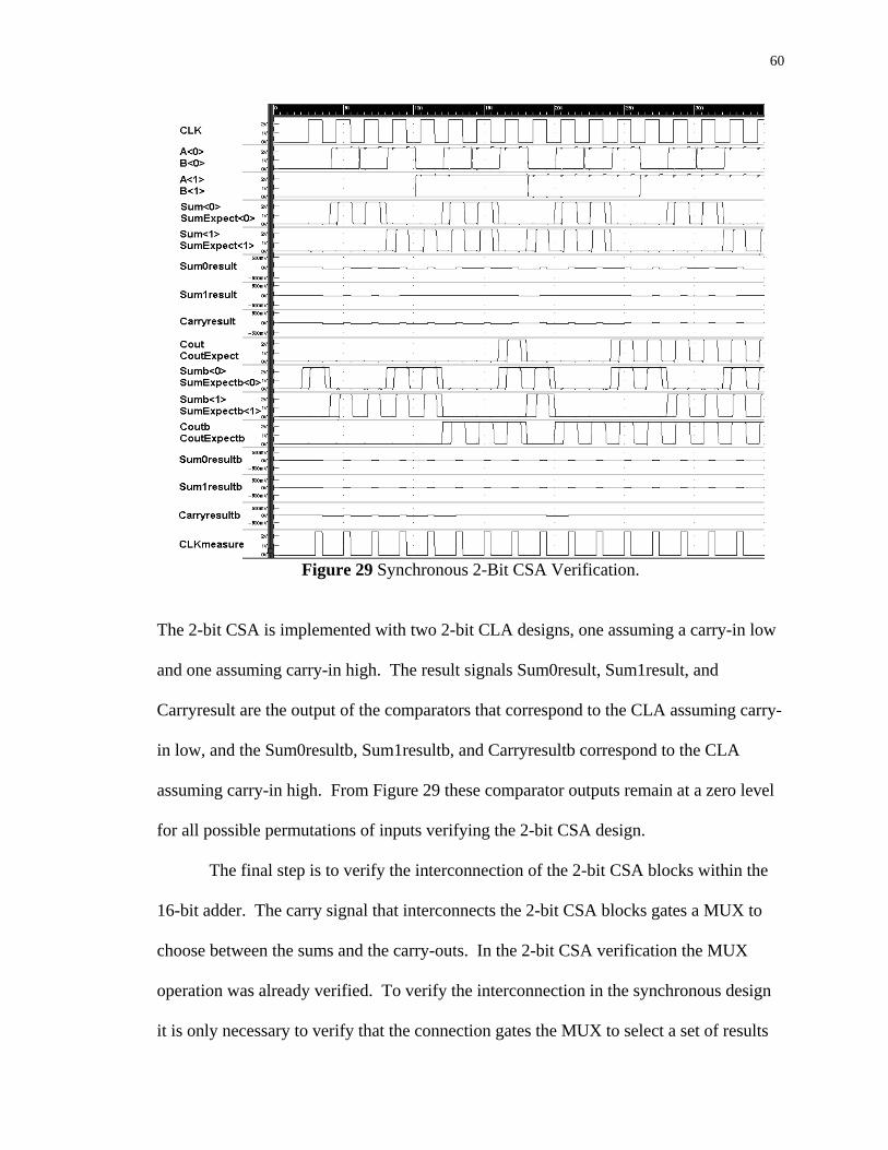
60
Figure 29 Synchronous 2-Bit CSA Verification.
The 2-bit CSA is implemented with two 2-bit CLA designs, one assuming a carry-in low
and one assuming carry-in high. The result signals Sum0result, Sum1result, and
Carryresult are the output of the comparators that correspond to the CLA assuming carry-
in low, and the Sum0resultb, Sum1resultb, and Carryresultb correspond to the CLA
assuming carry-in high. From Figure 29 these comparator outputs remain at a zero level
for all possible permutations of inputs verifying the 2-bit CSA design.
The final step is to verify the interconnection of the 2-bit CSA blocks within the
16-bit adder. The carry signal that interconnects the 2-bit CSA blocks gates a MUX to
choose between the sums and the carry-outs. In the 2-bit CSA verification the MUX
operation was already verified. To verify the interconnection in the synchronous design
it is only necessary to verify that the connection gates the MUX to select a set of results
61
for each 2-bit block. Therefore only one correct 16-bit addition was required to finish the
synchronous design verification.
4.2.4 Synchronous Worse Case Computation Time
The final step in testing the synchronous design is to find the worse case
computation time. This delay defines the maximum speed at which the synchronous
adder may operate. As was pointed out in the design verification, it is unreasonable to
use all possible permutations of inputs. Using the knowledge of the synchronous adder
architecture a reduced number of input combinations is developed.
The synchronous 16-bit adder is constructed with one 2-bit CLA as the first 2-bit
block and then the remaining seven 2-bit blocks are 2-bit CSAs. Each 2-bit CSA
calculates the sums and the carry-out for the 2-bit block for both possible values of carry-
in. Therefore, the CSA computation delay is independent on the carry-in from the
previous 2-bit block. Based on this observation the 2-bit CSA worse case computation
time uses the same data condition for the first six 2-bit CSA blocks. The delay between
these six is associated with the carry-out signals. The seventh 2-bit CSA worse case
delay is associated with the sum computation.
From this discussion the synchronous 16-bit adder is divided into three test
sections. The three sections are the first 2-bit CLA block, the next six 2-bit CSA blocks,
and the final 2-bit CSA block. Each section is tested with all possible input permutations
giving a reduced number of test vectors. The total number of binary input sources
required is thirteen, four binary inputs per test section and one carry-in value. The total
number of permutations is then 213 or 8192. Using these permutations the synchronous
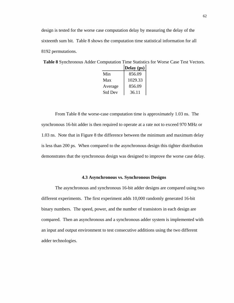
62
design is tested for the worse case computation delay by measuring the delay of the
sixteenth sum bit. Table 8 shows the computation time statistical information for all
8192 permutations.
Table 8 Synchronous Adder Computation Time Statistics for Worse Case Test Vectors. Delay (ps)
Min 856.09Max 1029.33Average 856.09Std Dev 36.11
From Table 8 the worse-case computation time is approximately 1.03 ns. The
synchronous 16-bit adder is then required to operate at a rate not to exceed 970 MHz or
1.03 ns. Note that in Figure 8 the difference between the minimum and maximum delay
is less than 200 ps. When compared to the asynchronous design this tighter distribution
demonstrates that the synchronous design was designed to improve the worse case delay.
4.3 Asynchronous vs. Synchronous Designs
The asynchronous and synchronous 16-bit adder designs are compared using two
different experiments. The first experiment adds 10,000 randomly generated 16-bit
binary numbers. The speed, power, and the number of transistors in each design are
compared. Then an asynchronous and a synchronous adder system is implemented with
an input and output environment to test consecutive additions using the two different
adder technologies.
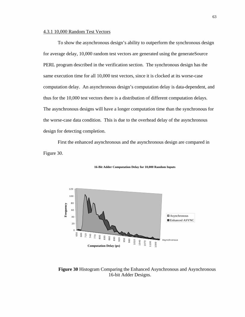
63
4.3.1 10,000 Random Test Vectors
To show the asynchronous design’s ability to outperform the synchronous design
for average delay, 10,000 random test vectors are generated using the generateSource
PERL program described in the verification section. The synchronous design has the
same execution time for all 10,000 test vectors, since it is clocked at its worse-case
computation delay. An asynchronous design’s computation delay is data-dependent, and
thus for the 10,000 test vectors there is a distribution of different computation delays.
The asynchronous designs will have a longer computation time than the synchronous for
the worse-case data condition. This is due to the overhead delay of the asynchronous
design for detecting completion.
First the enhanced asynchronous and the asynchronous design are compared in
Figure 30.
650
680
710
740
770
800
830
860
890
920
950
980
1010
1040
1070
1100
1300
Asynchronous
0
20
40
60
80
100
120
Freq
uenc
y
Computation Delay (ps)
16-Bit Adder Computation Delay for 10,000 Random Inputs
AsynchronousEnhanced ASYNC
Figure 30 Histogram Comparing the Enhanced Asynchronous and Asynchronous
16-bit Adder Designs.
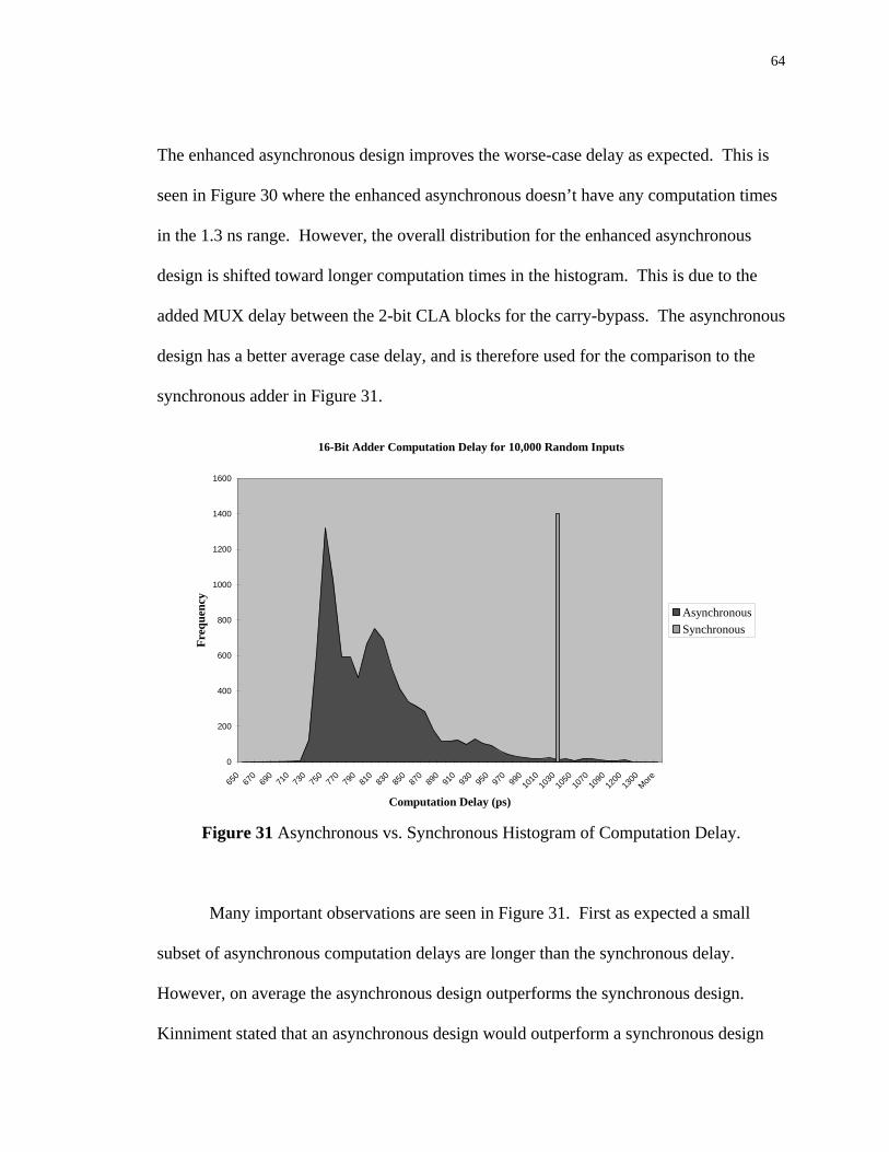
64
The enhanced asynchronous design improves the worse-case delay as expected. This is
seen in Figure 30 where the enhanced asynchronous doesn’t have any computation times
in the 1.3 ns range. However, the overall distribution for the enhanced asynchronous
design is shifted toward longer computation times in the histogram. This is due to the
added MUX delay between the 2-bit CLA blocks for the carry-bypass. The asynchronous
design has a better average case delay, and is therefore used for the comparison to the
synchronous adder in Figure 31.
16-Bit Adder Computation Delay for 10,000 Random Inputs
0
200
400
600
800
1000
1200
1400
1600
650
670
690
710
730
750
770
790
810
830
850
870
890
910
930
950
970
990
1010
1030
1050
1070
1090
1200
1300
More
Computation Delay (ps)
Freq
uenc
y
AsynchronousSynchronous
Figure 31 Asynchronous vs. Synchronous Histogram of Computation Delay.
Many important observations are seen in Figure 31. First as expected a small
subset of asynchronous computation delays are longer than the synchronous delay.
However, on average the asynchronous design outperforms the synchronous design.
Kinniment stated that an asynchronous design would outperform a synchronous design
65
for random data, but that for real data a synchronous design would outperform an
asynchronous design [5]. Kinniment observed that real data is skewed towards the worse
case delay rather than the average delay [5]. If the histogram in Figure 31 is truly based
on evenly distributed random data, this graph clearly shows that this is not the case. The
number of asynchronous computation delays that exceeds the synchronous computations
is about 1% of the 10,000 random inputs. Therefore even if real data is skewed towards
the worse-case the asynchronous design would still outperform the synchronous design.
For the synchronous to outperform the asynchronous design, the real data would have to
be skewed towards the top 1% of computation delays.
Another observation is the benefit of the synchronous design using the CSA. If
the synchronous adder design used the same architecture as the asynchronous, then the
synchronous computation time in Figure 31 would match the slowest asynchronous time
minus the completion detection delay. In this asynchronous design the maximum
completion detection delay is approximately 80 ps. This would result in a synchronous
design with a computation delay around 1.2 ns as compared to 1.03ns for the CSA design.
By using the CSA in the synchronous design, it enables the synchronous adder to achieve
higher performance. This supports my design decision to use different adder
architectures that allow the design technologies to realize the best performance.
Table 9 compares the average and worse case delay, power, and the number of
transistors in the three 16-bit adder designs. The average and worse case delays
summarize the same results already discussed in the histograms. As expected the
enhanced asynchronous design with carry-bypass consumes a little more power than the
asynchronous, due to the extra circuitry required for the bypass. The synchronous design
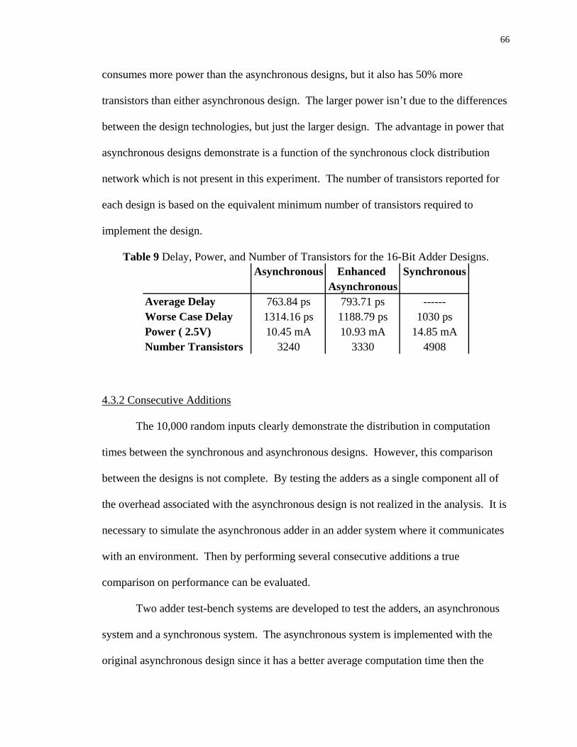
66
consumes more power than the asynchronous designs, but it also has 50% more
transistors than either asynchronous design. The larger power isn’t due to the differences
between the design technologies, but just the larger design. The advantage in power that
asynchronous designs demonstrate is a function of the synchronous clock distribution
network which is not present in this experiment. The number of transistors reported for
each design is based on the equivalent minimum number of transistors required to
implement the design.
Table 9 Delay, Power, and Number of Transistors for the 16-Bit Adder Designs. Asynchronous Enhanced Synchronous
AsynchronousAverage Delay 763.84 ps 793.71 ps ------Worse Case Delay 1314.16 ps 1188.79 ps 1030 psPower ( 2.5V) 10.45 mA 10.93 mA 14.85 mANumber Transistors 3240 3330 4908
4.3.2 Consecutive Additions
The 10,000 random inputs clearly demonstrate the distribution in computation
times between the synchronous and asynchronous designs. However, this comparison
between the designs is not complete. By testing the adders as a single component all of
the overhead associated with the asynchronous design is not realized in the analysis. It is
necessary to simulate the asynchronous adder in an adder system where it communicates
with an environment. Then by performing several consecutive additions a true
comparison on performance can be evaluated.
Two adder test-bench systems are developed to test the adders, an asynchronous
system and a synchronous system. The asynchronous system is implemented with the
original asynchronous design since it has a better average computation time then the
67
enhanced asynchronous design. The system designs are tested using thirty-two
consecutive additions.
4.3.2.1 Asynchronous System Design
The asynchronous system design involves developing an asynchronous input and
output environment. The input environment is required to hold the binary data for the
thirty-two consecutive additions. After each addition is complete the input environment
provides the next two 16-bit binary numbers to the adder and the next carry-in. The
output environment captures the addition results.
The input environment is implemented using an ideal shift register. An ideal
design is used, because we are not concerned with testing a shift register design, but
rather just require its functionality. The ideal shift register is implemented in a master-
slave latch style using voltage-controlled resistors for switches, voltage-controlled
voltage sources for drivers, and capacitors to store data. The shift registers are designed
to allow a parallel load of all bits at the beginning of a simulation using the Load signal.
The asynchronous input environment has thirty-three 32-bit shift registers, one for each
bit in the 16-bit binary numbers, and one for the carry-in. See Appendix C for a
schematic of the ideal 8-bit shift register used to construct the 32-bit shift registers.
The input environment requires asynchronous communication logic to facilitate
communication with the asynchronous adder. The input environment asynchronous
communication is defined by the burstmode machine in Figure 32.
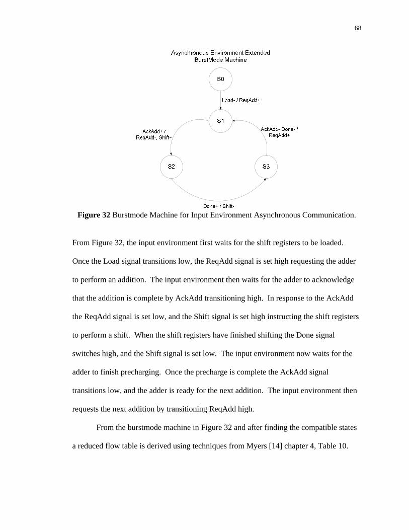
68
Figure 32 Burstmode Machine for Input Environment Asynchronous Communication.
From Figure 32, the input environment first waits for the shift registers to be loaded.
Once the Load signal transitions low, the ReqAdd signal is set high requesting the adder
to perform an addition. The input environment then waits for the adder to acknowledge
that the addition is complete by AckAdd transitioning high. In response to the AckAdd
the ReqAdd signal is set low, and the Shift signal is set high instructing the shift registers
to perform a shift. When the shift registers have finished shifting the Done signal
switches high, and the Shift signal is set low. The input environment now waits for the
adder to finish precharging. Once the precharge is complete the AckAdd signal
transitions low, and the adder is ready for the next addition. The input environment then
requests the next addition by transitioning ReqAdd high.
From the burstmode machine in Figure 32 and after finding the compatible states
a reduced flow table is derived using techniques from Myers [14] chapter 4, Table 10.
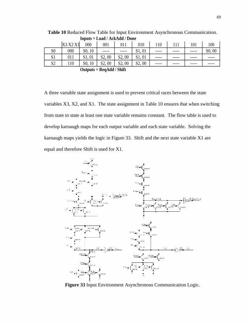
69
Table 10 Reduced Flow Table for Input Environment Asynchronous Communication. Inputs = Load / AckAdd / Done
X3 X2 X1 000 001 011 010 110 111 101 100S0 000 S0, 10 ----- ----- S1, 01 ----- ----- ----- S0, 00S1 011 S1, 01 S2, 00 S2, 00 S1, 01 ----- ----- ----- -----S2 110 S0, 10 S2, 00 S2, 00 S2, 00 ----- ----- ----- -----
Outputs = ReqAdd / Shift
A three variable state assignment is used to prevent critical races between the state
variables X3, X2, and X1. The state assignment in Table 10 ensures that when switching
from state to state at least one state variable remains constant. The flow table is used to
develop karnaugh maps for each output variable and each state variable. Solving the
karnaugh maps yields the logic in Figure 33. Shift and the next state variable X1 are
equal and therefore Shift is used for X1.
Figure 33 Input Environment Asynchronous Communication Logic.
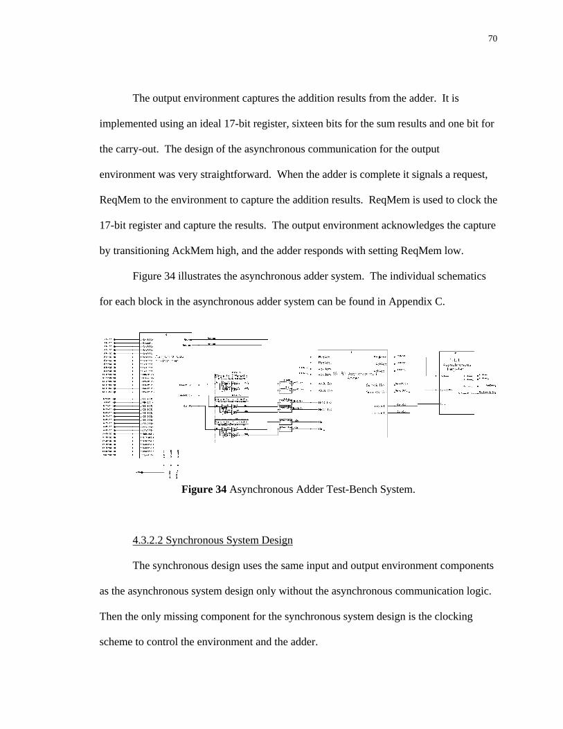
70
The output environment captures the addition results from the adder. It is
implemented using an ideal 17-bit register, sixteen bits for the sum results and one bit for
the carry-out. The design of the asynchronous communication for the output
environment was very straightforward. When the adder is complete it signals a request,
ReqMem to the environment to capture the addition results. ReqMem is used to clock the
17-bit register and capture the results. The output environment acknowledges the capture
by transitioning AckMem high, and the adder responds with setting ReqMem low.
Figure 34 illustrates the asynchronous adder system. The individual schematics
for each block in the asynchronous adder system can be found in Appendix C.
Figure 34 Asynchronous Adder Test-Bench System.
4.3.2.2 Synchronous System Design
The synchronous design uses the same input and output environment components
as the asynchronous system design only without the asynchronous communication logic.
Then the only missing component for the synchronous system design is the clocking
scheme to control the environment and the adder.
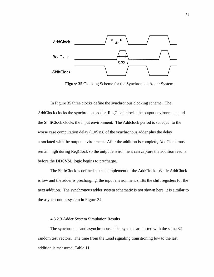
71
Figure 35 Clocking Scheme for the Synchronous Adder System.
In Figure 35 three clocks define the synchronous clocking scheme. The
AddClock clocks the synchronous adder, RegClock clocks the output environment, and
the ShiftClock clocks the input environment. The Addclock period is set equal to the
worse case computation delay (1.05 ns) of the synchronous adder plus the delay
associated with the output environment. After the addition is complete, AddClock must
remain high during RegClock so the output environment can capture the addition results
before the DDCVSL logic begins to precharge.
The ShiftClock is defined as the complement of the AddClock. While AddClock
is low and the adder is precharging, the input environment shifts the shift registers for the
next addition. The synchronous adder system schematic is not shown here, it is similar to
the asynchronous system in Figure 34.
4.3.2.3 Adder System Simulation Results
The synchronous and asynchronous adder systems are tested with the same 32
random test vectors. The time from the Load signaling transitioning low to the last
addition is measured, Table 11.
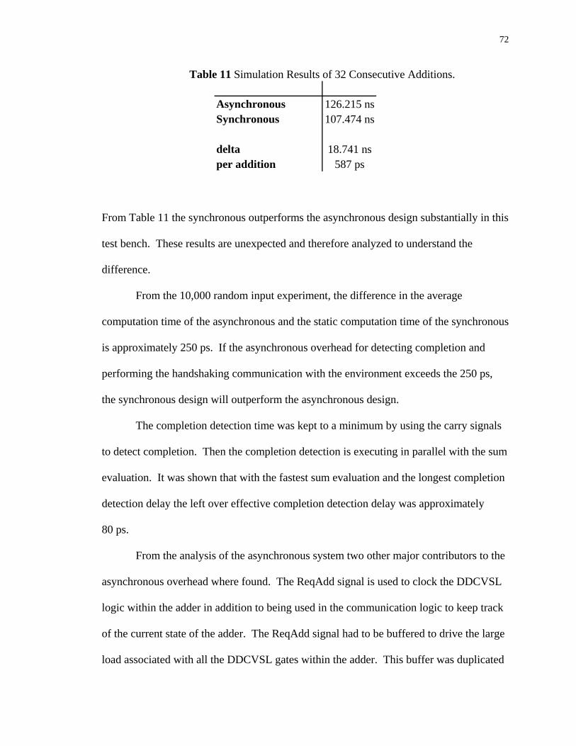
72
Table 11 Simulation Results of 32 Consecutive Additions.
Asynchronous 126.215 nsSynchronous 107.474 ns
delta 18.741 nsper addition 587 ps
From Table 11 the synchronous outperforms the asynchronous design substantially in this
test bench. These results are unexpected and therefore analyzed to understand the
difference.
From the 10,000 random input experiment, the difference in the average
computation time of the asynchronous and the static computation time of the synchronous
is approximately 250 ps. If the asynchronous overhead for detecting completion and
performing the handshaking communication with the environment exceeds the 250 ps,
the synchronous design will outperform the asynchronous design.
The completion detection time was kept to a minimum by using the carry signals
to detect completion. Then the completion detection is executing in parallel with the sum
evaluation. It was shown that with the fastest sum evaluation and the longest completion
detection delay the left over effective completion detection delay was approximately
80 ps.
From the analysis of the asynchronous system two other major contributors to the
asynchronous overhead where found. The ReqAdd signal is used to clock the DDCVSL
logic within the adder in addition to being used in the communication logic to keep track
of the current state of the adder. The ReqAdd signal had to be buffered to drive the large
load associated with all the DDCVSL gates within the adder. This buffer was duplicated
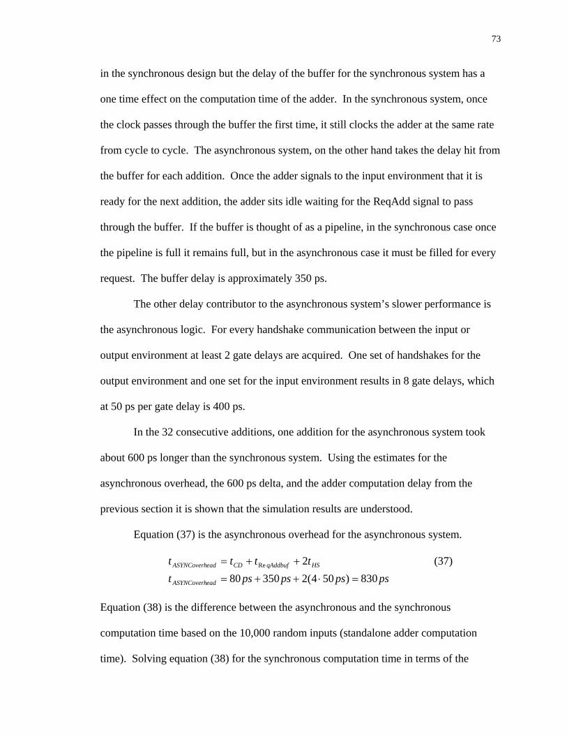
73
in the synchronous design but the delay of the buffer for the synchronous system has a
one time effect on the computation time of the adder. In the synchronous system, once
the clock passes through the buffer the first time, it still clocks the adder at the same rate
from cycle to cycle. The asynchronous system, on the other hand takes the delay hit from
the buffer for each addition. Once the adder signals to the input environment that it is
ready for the next addition, the adder sits idle waiting for the ReqAdd signal to pass
through the buffer. If the buffer is thought of as a pipeline, in the synchronous case once
the pipeline is full it remains full, but in the asynchronous case it must be filled for every
request. The buffer delay is approximately 350 ps.
The other delay contributor to the asynchronous system’s slower performance is
the asynchronous logic. For every handshake communication between the input or
output environment at least 2 gate delays are acquired. One set of handshakes for the
output environment and one set for the input environment results in 8 gate delays, which
at 50 ps per gate delay is 400 ps.
In the 32 consecutive additions, one addition for the asynchronous system took
about 600 ps longer than the synchronous system. Using the estimates for the
asynchronous overhead, the 600 ps delta, and the adder computation delay from the
previous section it is shown that the simulation results are understood.
Equation (37) is the asynchronous overhead for the asynchronous system.
HSqAddbufCDeadASYNCoverh tttt 2Re ++= (37) pspspspst eadASYNCoverh 830)504(235080 =⋅++=
Equation (38) is the difference between the asynchronous and the synchronous
computation time based on the 10,000 random inputs (standalone adder computation
time). Solving equation (38) for the synchronous computation time in terms of the
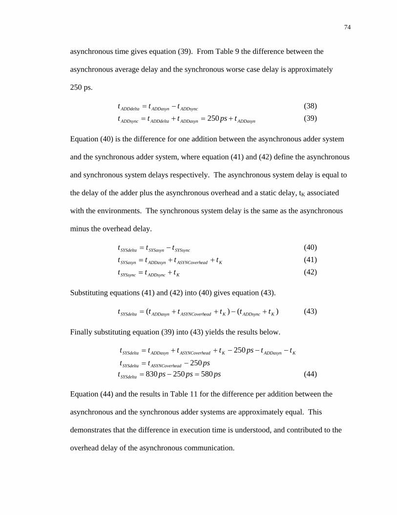
74
asynchronous time gives equation (39). From Table 9 the difference between the
asynchronous average delay and the synchronous worse case delay is approximately
250 ps.
ADDsyncADDasynADDdelta ttt −= (38)
ADDasynADDasynADDdeltaADDsync tpsttt +=+= 250 (39)
Equation (40) is the difference for one addition between the asynchronous adder system
and the synchronous adder system, where equation (41) and (42) define the asynchronous
and synchronous system delays respectively. The asynchronous system delay is equal to
the delay of the adder plus the asynchronous overhead and a static delay, tK associated
with the environments. The synchronous system delay is the same as the asynchronous
minus the overhead delay.
SYSsyncSYSasynSYSdelta ttt −= (40)
KeadASYNCoverhADDasynSYSasyn tttt ++= (41)
KADDsyncSYSsync ttt += (42) Substituting equations (41) and (42) into (40) gives equation (43).
)()( KADDsyncKeadASYNCoverhADDasynSYSdelta tttttt +−++= (43)
Finally substituting equation (39) into (43) yields the results below.
pstt
ttpstttt
eadASYNCoverhSYSdelta
KADDasynKeadASYNCoverhADDasynSYSdelta
250250
−=
−−−++=
pspspstSYSdelta 580250830 =−= (44)
Equation (44) and the results in Table 11 for the difference per addition between the
asynchronous and the synchronous adder systems are approximately equal. This
demonstrates that the difference in execution time is understood, and contributed to the
overhead delay of the asynchronous communication.
75
CHAPTER 5 - CONCLUSIONS
Two experiments were used to evaluate the adder designs. In the first experiment
the static synchronous adder computation delay, which is set to the worse case delay of
the synchronous adder is compared to the asynchronous computation delay distribution
for 10,000 random input permutations. The 10,000 random inputs are assumed to be an
evenly distributed random representation of all possible input permutations. In this
experiment the asynchronous adder’s average computation delay from the random inputs
outperforms the synchronous design by more than 250 ps. Comparing the adders as
standalone blocks, however doesn’t account for the asynchronous adder’s overhead delay
associated with an asynchronous design. The asynchronous overhead delay includes the
delay for completion detection, and the asynchronous communication with the
environment.
In a second experiment the adders are implemented into an adder system. In the
adder system an input and output environment provide the binary numbers and capture
the results for each addition. In this experiment to compare the performance of the two
adder designs, 32 consecutive additions are performed. For the 32 consecutive additions
the synchronous design outperforms the asynchronous design by more than 500 ps per
addition. In order for the asynchronous design to have better performance than the
synchronous, either the difference between the synchronous design worse case delay and
the asynchronous average delay must be larger, or the asynchronous overhead delay must
be smaller.
76
Using the carry-select adder (CSA) architecture for the synchronous adder design
required 50% more transistors than the asynchronous adder design. Both designs were
designed independently to give each design the opportunity to outperform the other.
With the larger number of transistors, the synchronous design has an unfair advantage.
Using an architecture for the synchronous that has a more comparable number of
transistors might yield different results.
A final observation, for a larger bit adder the asynchronous adder system will
outperform the synchronous adder system. For example doubling the number of bits in
the adders from sixteen to thirty-two, the computation time for the synchronous design
would double. The asynchronous system computation time would increase, but not
double. For the asynchronous system the asynchronous overhead delay would remain
mostly unchanged with only the completion detection delay increasing slightly. At the
point that the asynchronous overhead delay is less than the difference between the
asynchronous adder average computation and the synchronous computation delay, the
asynchronous adder design begins to demonstrate a performance advantage. For the 16-
bit adder system designs the synchronous outperforms the asynchronous by
approximately 850 ps with the asynchronous average computation delay 250 ps faster
than the synchronous design. Using these numbers a 64-bit asynchronous adder system
would outperform a 64-bit synchronous adder system using the corresponding adder
designs presented in this thesis.
The goal of this thesis was to show a high-speed performance advantage between
asynchronous and synchronous design technologies. It is demonstrated that neither
design technology clearly outperforms the other. Choosing between an asynchronous or
77
synchronous design implementation for high-speed performance completely depends on
the design specifics and the implementation.
78
REFERENCES
[1] D. Johnson and V. Akella, “Design and Analysis of Asychronous Adders,” IEE Proceedings on Computers and Digital Techniques, vol. 145, pp. 1-8, Jan. 1998.
[2] Kwen-Siong Chong, Bah-Hwee Gwee, and Joseph S. Chang, “Low-voltage
Asynchronous Adders for Low Power and High Speed Applications,” IEEE International Symposium on Circuits and Systems, vol. 1, pp. 873-876, May 2002.
[3] M. Renaudin and B. El Hassan, “The Design of Fast Asynchronous Adder
Structures and Their Implementations Using DCVS logic,” Proceedings of the 1994 IEEE International Symposium on Circuits and Systems, vol. 4, pp. 291-294, 1994.
[4] Mark A. Franklin and Tienyo Pan, “Performance Comparison of Asynchronous
Adders,” Proceedings IEEE International Symposium on Advanced Research in Asynchronous Circuits and Systems, pp. 117-125, November 1994.
[5] D. J. Kinniment, “An Evaluation of Asynchronous Addition,” IEEE Trans. VLSI
Systems, v4, no. 1, pp. 137-140, 1996. [6] Fu-Chiung Cheng, Stephen H. Unger, and Michael Theobald, “Self-Timed Carry-
Lookahead Adders,” IEEE Transactions on Computers, vol. 49, no. 7, pp. 659-672, July 2000.
[7] Gustavo A. Ruiz, “Evaluation of Three 32-Bit CMOS Adders in DCVS Logic for
Self-Timed Circuits,” IEEE Journal of Solid-State Circuits, vol. 33, no. 4, pp. 604-613, April 1998.
[8] Jan M. Rabaey, Digital Integrated Circuits, A Design Perspective, Prentice Hall,
1996. [9] Inseok S. Hwang and Aaron L. Fisher, “Ultrafast Compact 32-bit CMOS Adders
in Multiple-Output Domino Logic,” IEEE Journal of Solid-State Circuits, vol. 24, no. 2, pp. 358-369, April 1989.
[10] Kan M. Chu and David L. Pulfrey, “A Comparison of CMOS Circuit Techniques:
Differential Cascode Voltage Switch Logic Versus Conventional Logic,” IEEE J. Solid-State Circuits, vol. Sc-22, no. 4, pp. 528-532, August 1987.
[11] Pius Ng, Poras T. Balsara, and Don Steiss, “Performance of CMOS Differential -
Circuits,” IEEE Journal of Solid-State Circuits, vol. 31, no. 6, pp. 841-846, June 1996.
79
[12] Ivan Sutherland, Bob Sproull, and David Harris, Logical Effort: Designing Fast CMOS Circuits, Academic Press, 1999, pp 215.
[13] Kan M. Chu and David L. Pulfrey, “Design Procedures for Differential Cascode
Voltage Switch Circuits,” IEEE J. Solid-State Circuits, vol. Sc-21, pp. 159-164, December 1986.
[14] Chris J. Myers, Asynchronous Circuit Design, John Wiley & Sons, 2001. [15] R. J. Baker, H.W. Li, and D. E. Boyce, CMOS: Circuit Design, Layout, and
Simulation, IEEE Press, 1998. [16] Fu-Chiung Cheng, “Practical Design and Performance Evaluation of Completion
Detection Circuits,” Proceedings of International Conference on Computer Design, pp. 354-359, October 1998.
[17] Steven M. Nowick, Kenneth Y. Yun, Peter A. Beerel, and Ayoob E. Dooply,
“Speculative Completion for the Design of High-Performance Asynchronous Dynamic Adders,” Proceedings of The Third International Symposium on Advanced Research in asynchronous Circuits and Systems, pp. 210-223, April 1997.
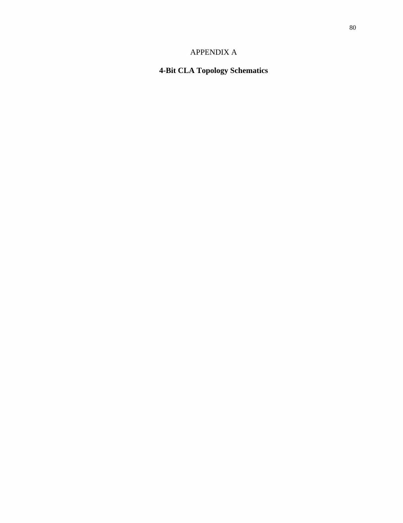
80
APPENDIX A
4-Bit CLA Topology Schematics
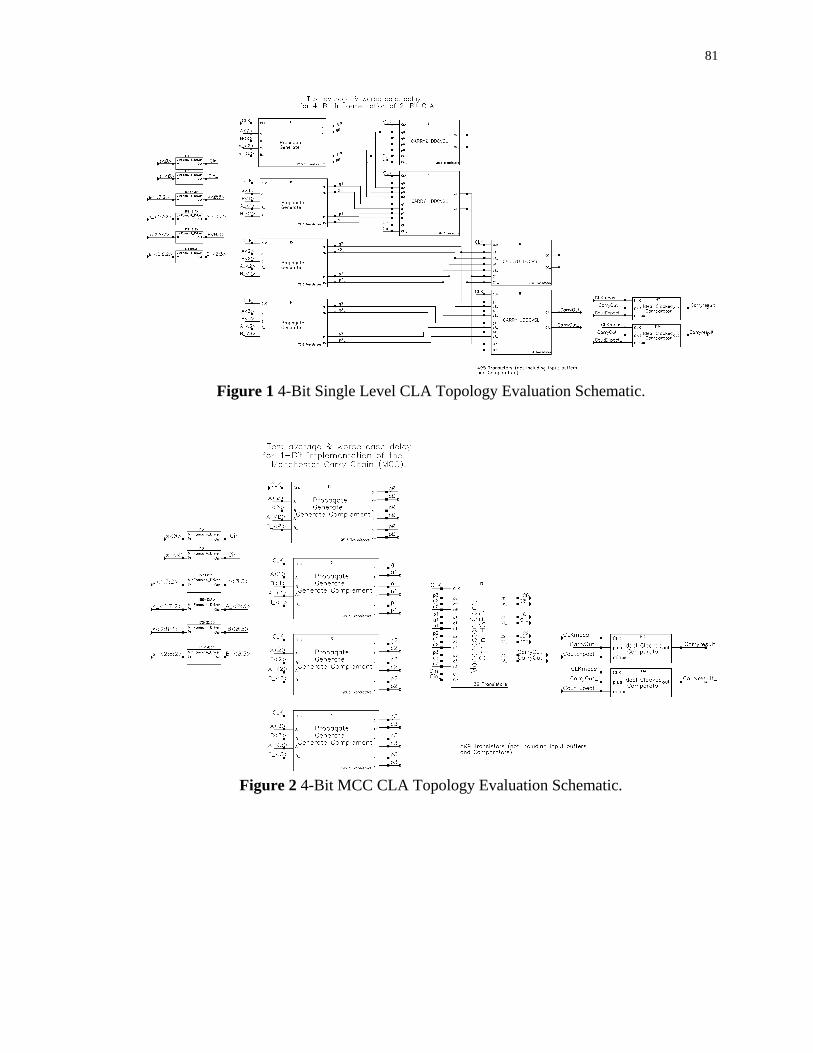
81
Figure 1 4-Bit Single Level CLA Topology Evaluation Schematic.
Figure 2 4-Bit MCC CLA Topology Evaluation Schematic.
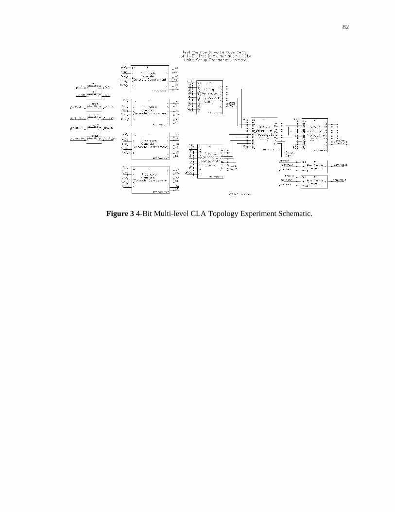
82
Figure 3 4-Bit Multi-level CLA Topology Experiment Schematic.
83
APPENDIX B
generateSource PERL Code
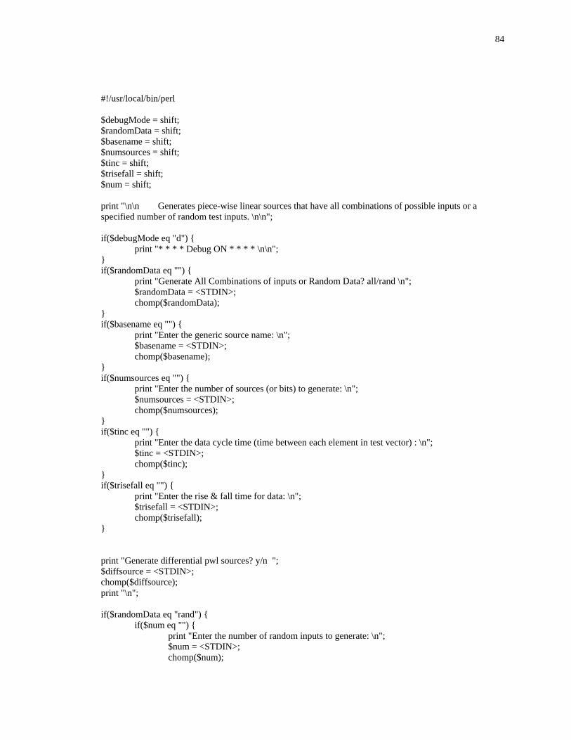
84
#!/usr/local/bin/perl $debugMode = shift; $randomData = shift; $basename = shift; $numsources = shift; $tinc = shift; $trisefall = shift; $num = shift; print "\n\n Generates piece-wise linear sources that have all combinations of possible inputs or a specified number of random test inputs. \n\n"; if($debugMode eq "d") { print "* * * * Debug ON * * * * \n\n"; } if($randomData eq "") { print "Generate All Combinations of inputs or Random Data? all/rand \n"; $randomData = <STDIN>; chomp($randomData); } if($basename eq "") { print "Enter the generic source name: \n"; $basename = <STDIN>; chomp($basename); } if($numsources eq "") { print "Enter the number of sources (or bits) to generate: \n"; $numsources = <STDIN>; chomp($numsources); } if($tinc eq "") { print "Enter the data cycle time (time between each element in test vector) : \n"; $tinc = <STDIN>; chomp($tinc); } if($trisefall eq "") { print "Enter the rise & fall time for data: \n"; $trisefall = <STDIN>; chomp($trisefall); } print "Generate differential pwl sources? y/n "; $diffsource = <STDIN>; chomp($diffsource); print "\n"; if($randomData eq "rand") { if($num eq "") { print "Enter the number of random inputs to generate: \n"; $num = <STDIN>; chomp($num);
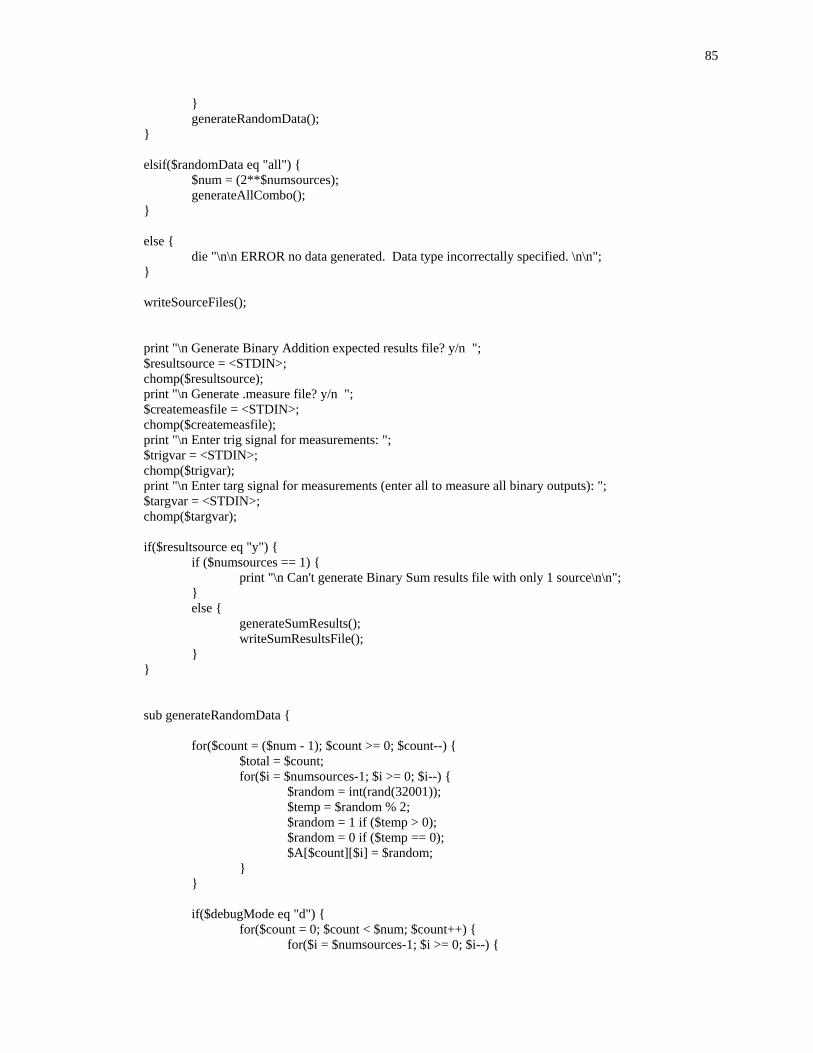
85
} generateRandomData(); } elsif($randomData eq "all") { $num = (2**$numsources); generateAllCombo(); } else { die "\n\n ERROR no data generated. Data type incorrectally specified. \n\n"; } writeSourceFiles(); print "\n Generate Binary Addition expected results file? y/n "; $resultsource = <STDIN>; chomp($resultsource); print "\n Generate .measure file? y/n "; $createmeasfile = <STDIN>; chomp($createmeasfile); print "\n Enter trig signal for measurements: "; $trigvar = <STDIN>; chomp($trigvar); print "\n Enter targ signal for measurements (enter all to measure all binary outputs): "; $targvar = <STDIN>; chomp($targvar); if($resultsource eq "y") { if ($numsources == 1) { print "\n Can't generate Binary Sum results file with only 1 source\n\n"; } else { generateSumResults(); writeSumResultsFile(); } } sub generateRandomData { for($count = ($num - 1); $count >= 0; $count--) { $total = $count; for($i = $numsources-1; $i >= 0; $i--) { $random = int(rand(32001)); $temp = $random % 2; $random = 1 if ($temp > 0); $random = 0 if ($temp == 0); $A[$count][$i] = $random; } } if($debugMode eq "d") { for($count = 0; $count < $num; $count++) { for($i = $numsources-1; $i >= 0; $i--) {
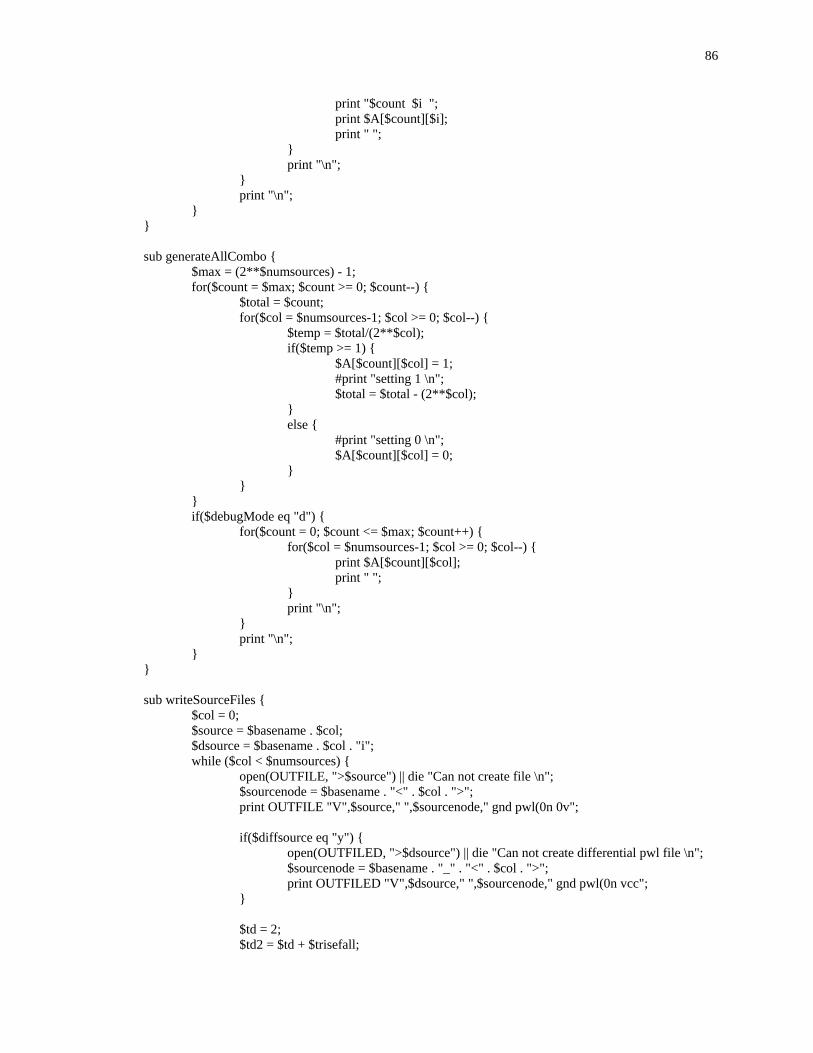
86
print "$count $i "; print $A[$count][$i]; print " "; } print "\n"; } print "\n"; } } sub generateAllCombo { $max = (2**$numsources) - 1; for($count = $max; $count >= 0; $count--) { $total = $count; for($col = $numsources-1; $col >= 0; $col--) { $temp = $total/(2**$col); if($temp >= 1) { $A[$count][$col] = 1; #print "setting 1 \n"; $total = $total - (2**$col); } else { #print "setting 0 \n"; $A[$count][$col] = 0; } } } if($debugMode eq "d") { for($count = 0; $count <= $max; $count++) { for($col = $numsources-1; $col >= 0; $col--) { print $A[$count][$col]; print " "; } print "\n"; } print "\n"; } } sub writeSourceFiles { $col = 0; $source = $basename . $col; $dsource = $basename . $col . "i"; while ($col < $numsources) { open(OUTFILE, ">$source") || die "Can not create file \n"; $sourcenode = $basename . "<" . $col . ">"; print OUTFILE "V",$source," ",$sourcenode," gnd pwl(0n 0v"; if($diffsource eq "y") { open(OUTFILED, ">$dsource") || die "Can not create differential pwl file \n"; $sourcenode = $basename . "_" . "<" . $col . ">"; print OUTFILED "V",$dsource," ",$sourcenode," gnd pwl(0n vcc"; } $td = 2; $td2 = $td + $trisefall;
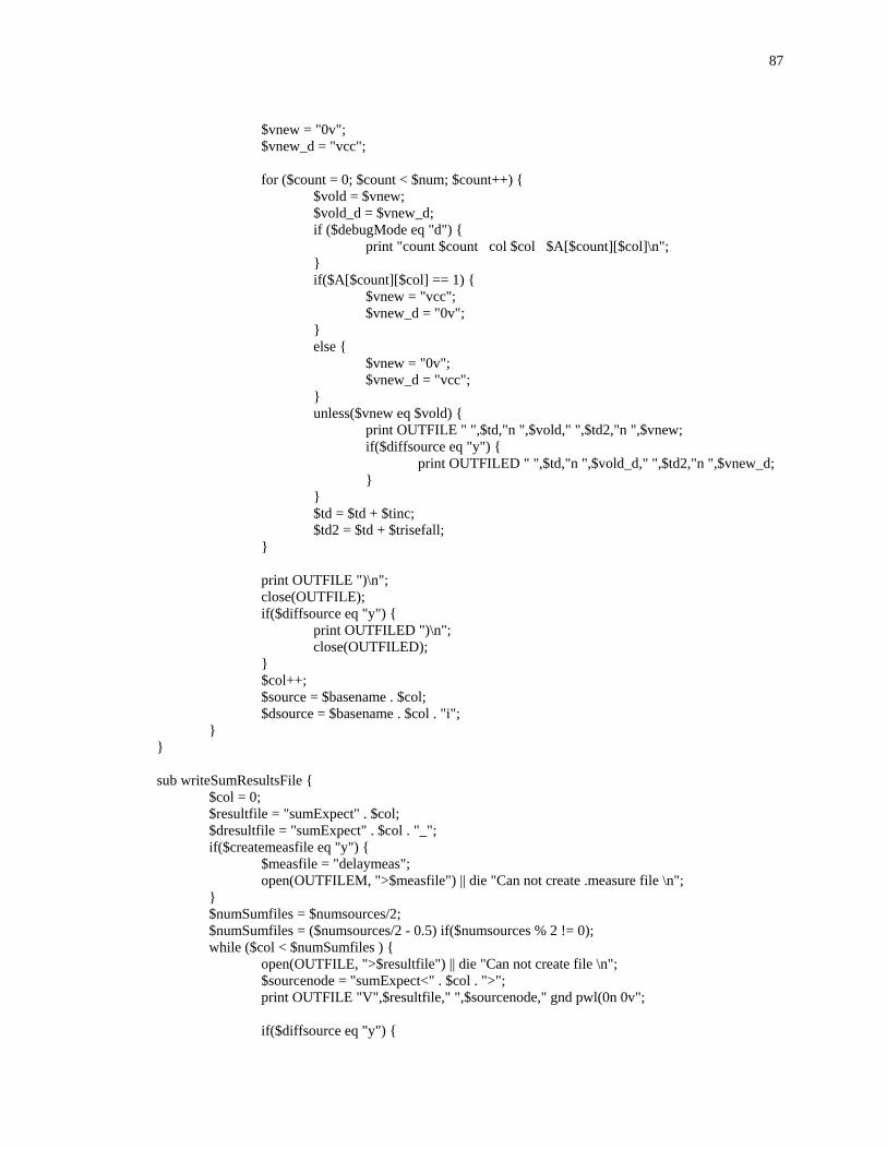
87
$vnew = "0v"; $vnew_d = "vcc"; for ($count = 0; $count < $num; $count++) { $vold = $vnew; $vold_d = $vnew_d; if ($debugMode eq "d") { print "count $count col $col $A[$count][$col]\n"; } if($A[$count][$col] == 1) { $vnew = "vcc"; $vnew_d = "0v"; } else { $vnew = "0v"; $vnew_d = "vcc"; } unless($vnew eq $vold) { print OUTFILE " ",$td,"n ",$vold," ",$td2,"n ",$vnew; if($diffsource eq "y") { print OUTFILED " ",$td,"n ",$vold_d," ",$td2,"n ",$vnew_d; } } $td = $td + $tinc; $td2 = $td + $trisefall; } print OUTFILE ")\n"; close(OUTFILE); if($diffsource eq "y") { print OUTFILED ")\n"; close(OUTFILED); } $col++; $source = $basename . $col; $dsource = $basename . $col . "i"; } } sub writeSumResultsFile { $col = 0; $resultfile = "sumExpect" . $col; $dresultfile = "sumExpect" . $col . "_"; if($createmeasfile eq "y") { $measfile = "delaymeas"; open(OUTFILEM, ">$measfile") || die "Can not create .measure file \n"; } $numSumfiles = $numsources/2; $numSumfiles = ($numsources/2 - 0.5) if($numsources % 2 != 0); while ($col < $numSumfiles ) { open(OUTFILE, ">$resultfile") || die "Can not create file \n"; $sourcenode = "sumExpect<" . $col . ">"; print OUTFILE "V",$resultfile," ",$sourcenode," gnd pwl(0n 0v"; if($diffsource eq "y") {
88
open(OUTFILED, ">$dresultfile") || die "Can not create differential pwl file \n"; $dsourcenode = "sumExpect_<" . $col . ">"; print OUTFILED "V",$dresultfile," ",$dsourcenode," gnd pwl(0n vcc"; } $td = 2; #always start at 2n $td2 = $td + $trisefall; $vnew = "0v"; $vnew_d = "vcc"; $rise = 0; $drise = 0; for ($count = 0; $count < $num; $count++) { $vold = $vnew; $vold_d = $vnew_d; if($debugMode eq "d") { print "count $count col $col $E[$count][$col]\n"; } if($E[$count][$col] == 1) { $vnew = "vcc"; $vnew_d = "0v"; if(($createmeasfile eq "y")&&($targvar eq "all")) { $rise++; print OUTFILEM ".meas tran m",$count,"sum",$col," trig ",$trigvar," td=2n val=1.25V rise=",$count+1," targ Sum<",$col,"> td=2n val=1.25V rise=",$rise," \n"; } } else { $vnew = "0v"; $vnew_d = "vcc"; if(($createmeasfile eq "y")&&($targvar eq "all")) { $drise++; print OUTFILEM ".meas tran m",$count,"sum_",$col," trig ",$trigvar," td=2n val=1.25V rise=",$count+1," targ Sum_<",$col,"> td=2n val=1.25V rise=",$drise," \n"; } } unless($vnew eq $vold) { print OUTFILE " ",$td,"n ",$vold," ",$td2,"n ",$vnew; if($diffsource eq "y") { print OUTFILED " ",$td,"n ",$vold_d," ",$td2,"n ",$vnew_d; } } $td = $td + $tinc; $td2 = $td + $trisefall; } print OUTFILE ")\n"; close(OUTFILE); if($diffsource eq "y") { print OUTFILED ")\n"; close(OUTFILED); } $col++; $resultfile = "sumExpect" . $col; $dresultfile = "sumExpect" . $col . "_"; }
89
#Write Carryout file results $carryfile = "CoutExpect"; $dcarryfile = "CoutExpect_"; open(OUTFILE, ">$carryfile") || die "Can not create file \n"; print OUTFILE "V",$carryfile," ",$carryfile," gnd pwl(0n 0v"; if($diffsource eq "y") { open(OUTFILED, ">$dcarryfile") || die "Can not create differential pwl file \n"; print OUTFILED "V",$dcarryfile," ",$dcarryfile," gnd pwl(0n vcc"; } $td = 2; $td2 = $td + $trisefall; $vnew = "0v"; $vnew_d = "vcc"; $rise = 0; $drise = 0; for ($count = 0; $count < $num; $count++) { $vold = $vnew; $vold_d = $vnew_d; if($C[$count] == 1) { $vnew = "vcc"; $vnew_d = "0v"; if(($createmeasfile eq "y")&&($targvar eq "all")) { $rise++; print OUTFILEM ".meas tran m",$count,"Cout trig ",$trigvar," td=2n val=1.25V rise=",$count+1," targ CarryOut td=2n val=1.25V rise=",$rise," \n"; } } else { $vnew = "0v"; $vnew_d = "vcc"; if($targvar eq "all") { if(($createmeasfile eq "y")&&($targvar eq "all")) { $drise++; print OUTFILEM ".meas tran m",$count,"Cout_ trig ",$trigvar," td=2n val=1.25V rise=",$count+1," targ CarryOut_ td=2n val=1.25V rise=",$drise," \n"; } } } unless($vnew eq $vold) { print OUTFILE " ",$td,"n ",$vold," ",$td2,"n ",$vnew; if($diffsource eq "y") { print OUTFILED " ",$td,"n ",$vold_d," ",$td2,"n ",$vnew_d; } } $td = $td + $tinc; $td2 = $td + $trisefall; if(($targvar ne "all")&&($createmeasfile eq "y")) { print OUTFILEM ".meas tran m",$count," trig ",$trigvar," td=2n val=1.25V rise=",$count+1," targ ",$targvar," td=2n val=1.25V fall=",$count+1," \n"; } } print OUTFILE ")\n"; close(OUTFILE); if($diffsource eq "y") { print OUTFILED ")\n";
90
close(OUTFILED); } if($createmeasfile eq "y") { print OUTFILEM "\n"; close(OUTFILEM); } } sub generateSumResults { if($numsources % 2 == 0) { print "\n Assume Carry-in is 0 or 1? 0/1 \n"; $AssumeCarry = <STDIN>; chomp($AssumeCarry); for($count = 0; $count < $num; $count++) { $cin = $AssumeCarry; for($col = 0; $col < $numsources/2; $col++) { $generate = $A[$count][($col*2)] * $A[$count][($col*2+1)]; $propagate = $A[$count][($col*2)] ^ $A[$count][($col*2+1)]; $E[$count][$col] = $propagate ^ $cin; $carry = $generate + ($propagate * $cin); $cin = $carry; } $C[$count] = $cin; } if($debugMode eq "d") { print "carryin = $AssumeCarry "; for($count = 0; $count < $num; $count++) { for($col = 0; $col < $numsources/2; $col++) { print "$A[$count][($col*2)] + $A[$count][($col*2+1)] "; print " = $E[$count][$col] \n"; } print "carryout is $C[$count] \n"; print "\n"; } print "\n"; } } else { print "\n Assume using 1st source for Carry-in.....\n\n"; for($count = 0; $count < $num; $count++) { $cin = $A[$count][0]; for($col = 1; $col < $numsources/2; $col++) { $generate = $A[$count][($col*2-1)] * $A[$count][($col*2)]; $propagate = $A[$count][($col*2-1)] ^ $A[$count][($col*2)]; $E[$count][$col-1] = $propagate ^ $cin; $carry = $generate + ($propagate * $cin); $cin = $carry; } $C[$count] = $cin; } if($debugMode eq "d") { for($count = 0; $count < $num; $count++) { print "carryin = $A[$count][0] \n";
91
for($col = 1; $col <= $numsources/2; $col++) { print "$A[$count][($col*2-1)] + $A[$count][($col*2)] "; print " = $E[$count][$col-1] \n"; } print "carryout is $C[$count] \n"; print "\n"; } print "\n"; } } } __END__
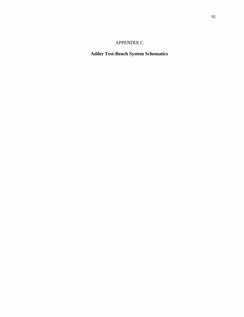
92
APPENDIX C
Adder Test-Bench System Schematics
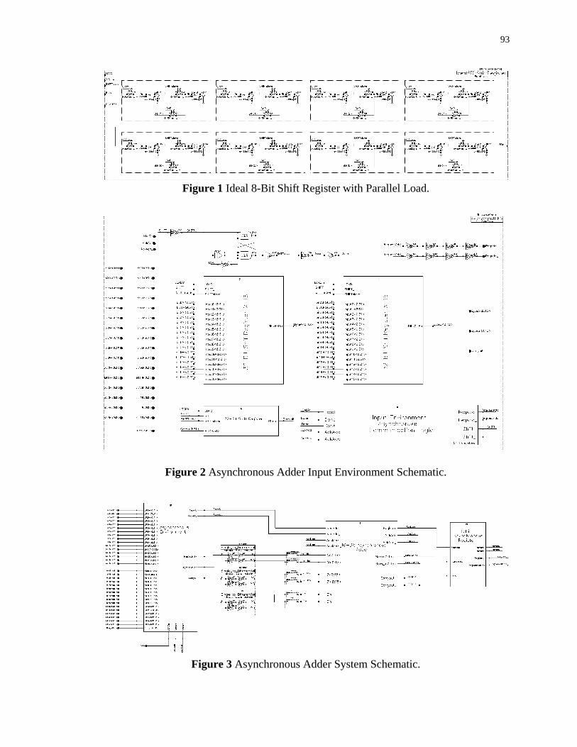
93
Figure 1 Ideal 8-Bit Shift Register with Parallel Load.
Figure 2 Asynchronous Adder Input Environment Schematic.
Figure 3 Asynchronous Adder System Schematic.