Embed Size (px)
Citation preview

Ultramicroscopy 89 (2001) 95–104
Comparison between experimental and computer simulationsof current–voltage (I–V) characteristics of dielectric-coated
photon-stimulated field emitters
Alexandre Mayera,*, M.S. Mousab,1, Jean-Pol Vignerona
aLaboratoire de Physique du Solide, Facult !es Universitaires Notre-Dame de la Paix, Rue de Bruxelles 61, B-5000 Namur, BelgiumbDepartment of Physics, M !utah University, Al-Karak, Jordan
Received 18 July 2000; received in revised form 2 November 2000
Abstract
For the purpose of simulating photon-stimulated field emission by taking account of three-dimensional aspects, atransfer-matrix formulation of electronic scattering was combined with a Floquet expansion of the wave function for
taking account of quanta exchanges between the electrons and the external radiation. With specific techniques topreserve numerical stability, this transfer-matrix formalism is well suited to compute the transmission of the field-emitted/photon-stimulated electrons between two electrodes.
This theory is applied to the computation of Fowler–Nordheim curves describing the photon-stimulated fieldemission of a tungsten plane emitter (described by zp0), which supports a nanometric protrusion and a dielectriccoating. The extraction bias ranges from 12 to 24V, for an inter-electrode distance of 4 nm. The electromagneticradiation has a wavelength of 0.67mm and a power flux density ranging from 5.96� 1010 to 5.96� 1012W/m2. The
effects due to the protrusion and the dielectric coating are studied. These theoretical results are compared with theexperimental data. r 2001 Elsevier Science B.V. All rights reserved.
1. Introduction
At present GaAs photomixers are usable at frequencies up to 1THz [1], but there are no wide-bandtunable sources for use at higher frequencies. Microfabricated triode field emitter arrays (FEA) offerpromise as microwave amplifiers [2]. However, thus far no FEA have been shown to have a gain exceedingunity above 1.3GHz [3], and this limit is attributed to shunting by capacitance of the gate structure.Previous simulations show that photomixing in resonant photon-assisted field emission could be used togenerate signals from DC to 100THz [4–9]. However, these signals occur at the apex of the tip, and so thereis the practical problem of how to efficiently couple the signals to an external load.
*Corresponding author. Tel.: +32-81-724720; fax: +32-81-724707.
E-mail address: [email protected] (A. Mayer).1On sabbatical leave.
0304-3991/01/$ - see front matter r 2001 Elsevier Science B.V. All rights reserved.
PII: S 0 3 0 4 - 3 9 9 1 ( 0 1 ) 0 0 1 0 5 - X

To modulate the emission current by means of an electromagnetic radiation efficiently, it is important tostudy how the sensitivity of this current to the power flux density of the radiation depends on parametersincluding the extraction bias, the geometry of the emitter and the presence of a dielectric coating. For thepurpose of taking account of three-dimensional aspects, the transfer-matrix formalism [10–15], used inprevious papers for the simulation [16–18] of the Fresnel projection microscope [19], was combined with aFloquet expansion [20] of the wave function for taking account of quanta exchanges between the electronsand the external radiation.
The derivation of this technique is presented in Section 2. It is then applied to the simulation of photon-stimulated field emission from a tungsten emitter. The application specifically focuses on the computationof the Fowler–Nordheim curves, for an electromagnetic radiation with fixed wavelength l=0.67 mm andvarious power flux densities. The simulation of the (time-dependent) potential-energy distribution aroundthe field-emission structure is described in Section 3. The results obtained with a plane emitter are comparedwith those obtained when it supports a metallic extension with 1 nm radius. A dielectric coating with 1 nmthickness is also considered. The results of the simulations are presented in Section 4. A comparison withthe experimental data obtained from metallic microemitters overlayed by a layer of dielectric coating ispresented in Section 5.
2. Theory of photon-stimulated field-emission
2.1. Basic formulation
Let us consider the following three-dimensional potential-energy distribution:
Vðr; tÞ ¼ VstatðrÞ þ VoscðrÞ cosðOtÞ; ð1Þ
which consists of a static part Vstat(r) and a time-dependent part Vosc(r) cos(Ot) representative of aradiation with frequency O [21].
Floquet’s theorem [20] is used to expand the wave function according to
Cðr; tÞ ¼XþN
k¼�N
CkðrÞe�iðEþk_OÞt=_: ð2Þ
By inserting this expression into the time-dependent Schr .odinger equation ½�_2=2mDþ Vðr; tÞ�Cðr; tÞ ¼i_@=@tCðr; tÞ; the components CkðrÞ of the wave function expansion (2) turn out to verify the exact set ofcoupled equations
�_2
2mDCkðrÞ þ VstatðrÞCkðrÞ þ 1
2VoscðrÞ½Ck�1ðrÞ þCkþ1ðrÞ� ¼ ðE þ k_OÞCkðrÞ: ð3Þ
This equation reveals that the time-dependent potential Vosc(r) cos(Ot) is responsible for photon-assistedcoupling to occur exclusively between wave function components whose associated energy values areseparated by a single quantum _O:
2.2. Consideration of n-fold symmetry
The wave function components CkðrÞ of expression (2) can be expanded in terms of basis functions thataccount for the f and r dependences. Their set is forced to be enumerable by specifying that the scatteringelectron remains localized inside a cylinder with radius R [22] in the three regions. One can thus write
CkðrÞ ¼Xm; j
Fðm; jÞ;kðzÞfðm; jÞðr;fÞ: ð4Þ
A. Mayer et al. / Ultramicroscopy 89 (2001) 95–10496

In this last expression, the two integer subscripts m and j enumerate the basis functions Cðm; jÞðr;fÞ; givenby
fðm; jÞðr;fÞ ¼Jm km; jr� �
eimfffiffiffiffiffiffiffiffiffiffiffiffiffiffiffiffiffiffiffiffiffiffiffiffiffiffiffiffiffiffiffiffiffiffiffiffiffiffiffiffiffiffiffiffiffiffiffiffi2pRR0 r Jm km; jr
� �� �2dr
q ð5Þ
and characterized by a radial wave vector km, j solution of Jm(km, jR)=0. The z dependence of the wavefunction is contained in the coefficients Fðm; jÞ;kðzÞ of the expansion.
By writing Vstat(r) and Vosc(r) like
Vstatðr;f; zÞ ¼ V0statðzÞ þ
XþN
q¼�N
%Vqstatðr; zÞe
iqnf; ð6Þ
Voscðr;f; zÞ ¼ V0oscðzÞ þ
XþN
q¼�N
%Vqoscðr; zÞe
iqnf; ð7Þ
the propagation equation (3) turns out to become,
�_2
2m
d2Fðm; jÞ;kðzÞdz2
þ V0statðzÞFðm; jÞ;kðzÞ þ 1
2V0osc Fðm; jÞ;kþ1ðzÞ þ Fðm; jÞ;k�1ðzÞ� �
þXq; j0
Sq; j0
m; j ðzÞFðm� qn; j0Þ; kðzÞ þ 12
Xq; j0
Oq; j0
m; jðzÞ Fðm�qn; j0Þ;kþ1ðzÞ þ Fðm�qn; j0Þ;k�1ðzÞ� �
¼ ðE þ k_O�_2
2mk2m; jÞFðm; jÞ;kðzÞ; ð8Þ
where the coupling coefficients Sq; j0
m; j ðzÞ and Oq; j0
m; jðzÞ are defined by the following expressions:
Sq; j0
m; j ðzÞ ¼
RR0 r %V
qstatðr; zÞJmðkm; jrÞJm�qnðkm�qn; j0rÞ drffiffiffiffiffiffiffiffiffiffiffiffiffiffiffiffiffiffiffiffiffiffiffiffiffiffiffiffiffiffiffiffiffiffiffiffiffiffiffiffiffiffiRR
0 r Jm km; jr� �� �2
drq ffiffiffiffiffiffiffiffiffiffiffiffiffiffiffiffiffiffiffiffiffiffiffiffiffiffiffiffiffiffiffiffiffiffiffiffiffiffiffiffiffiffiffiffiffiffiffiffiffiffiffiffiffiffiffiRR
0 r Jm�qn km�qn; j0r� �� �2
drq ; ð9Þ
Oq; j0
m; jðzÞ ¼
RR0 r %V
qoscðr; zÞJmðkm; jrÞJm�qnðkm�qn; j0rÞ drffiffiffiffiffiffiffiffiffiffiffiffiffiffiffiffiffiffiffiffiffiffiffiffiffiffiffiffiffiffiffiffiffiffiffiffiffiffiffiffiffiffiRR
0 r Jm km; jr� �� �2
drq ffiffiffiffiffiffiffiffiffiffiffiffiffiffiffiffiffiffiffiffiffiffiffiffiffiffiffiffiffiffiffiffiffiffiffiffiffiffiffiffiffiffiffiffiffiffiffiffiffiffiffiffiffiffiffiRR
0 r Jm�qn km�qn; j0r� �� �2
drq : ð10Þ
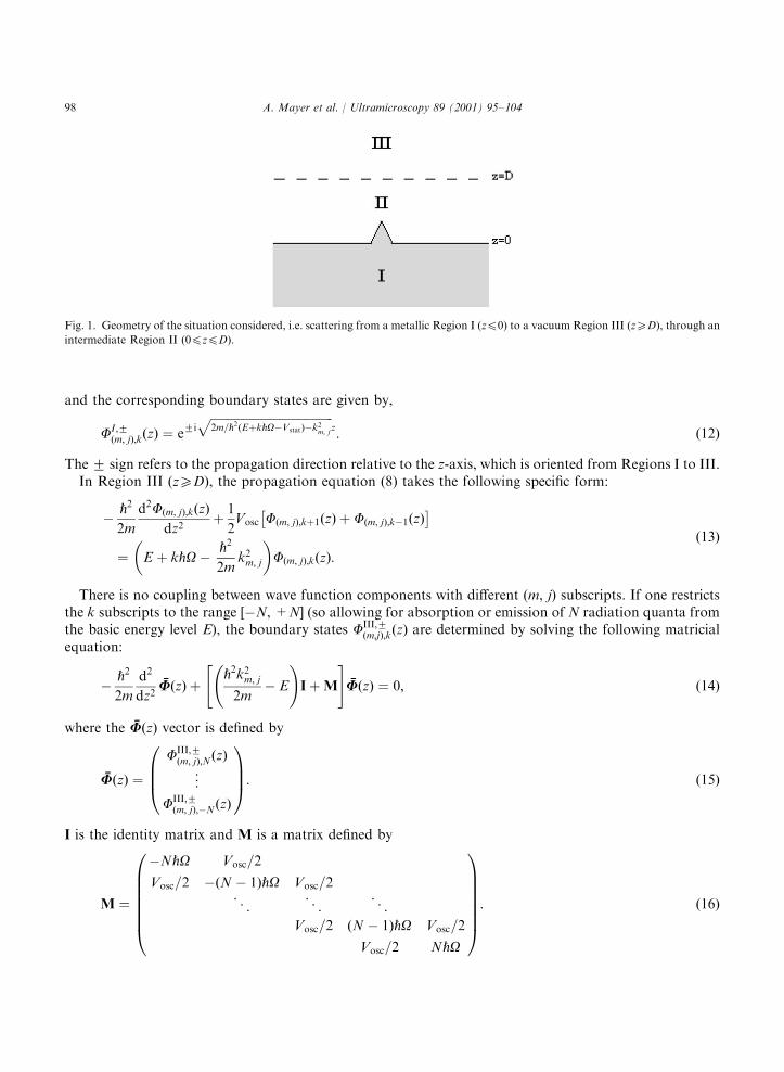
The propagation equation (8) can be implemented in a transfer-matrix procedure [23] in situations thatinvolve scattering from a (metallic) Region I (zp0) to a (vacuum) Region III (zXD), through anintermediate Region II (0pzpD). See Fig. 1 for an illustration.
2.3. Implementation of electronic scattering by transfer matrices
2.3.1. Boundary states for zp0 (Region I) and zXD (Region III)Let us assume the static part of the potential energy Vstat(r) to take a constant zero value in Region III
(zXD). It takes a constant non-zero value Vstat=eV�W�EF in Region I (zp0), where V is the extractionbias, W and EF, respectively, the work function and Fermi energy in this region. The time-dependent partof the potential energy Vosc(r) takes a constant zero value in Region I (zp0), since all electromagneticradiation is absorbed in this metallic region, and a constant non-zero value Vosc in Region III (zXD), wherethe electromagnetic field keeps interacting with traveling electrons.
In the metallic Region I (zp0), the propagation equation (8) then takes the specific form,
�_2
2m
d2Fðm; jÞ;kðzÞdz2
¼ ðE þ k_O� Vstat �_2m
k2m; jÞFðm; jÞ;kðzÞ ð11Þ
A. Mayer et al. / Ultramicroscopy 89 (2001) 95–104 97
and the corresponding boundary states are given by,
FI ;7ðm; jÞ;kðzÞ ¼ e
7iffiffiffiffiffiffiffiffiffiffiffiffiffiffiffiffiffiffiffiffiffiffiffiffiffiffiffiffiffiffiffiffiffiffiffiffiffiffiffiffiffi2m=_2ðEþk_O�VstatÞ�k2
m; j
pz: ð12Þ
The7 sign refers to the propagation direction relative to the z-axis, which is oriented from Regions I to III.In Region III (zXD), the propagation equation (8) takes the following specific form:
�_2
2m
d2Fðm; jÞ;kðzÞdz2
þ1
2Vosc Fðm; jÞ;kþ1ðzÞ þ Fðm; jÞ;k�1ðzÞ
� �¼ E þ k_O�
_2
2mk2m; j
�Fðm; jÞ;kðzÞ:
ð13Þ
There is no coupling between wave function components with different (m, j) subscripts. If one restrictsthe k subscripts to the range [�N, +N] (so allowing for absorption or emission of N radiation quanta fromthe basic energy level E), the boundary states FIII;7
ðm;jÞ;kðzÞ are determined by solving the following matricialequation:
�_2
2m
d2
dz2%UðzÞ þ
_2k2m; j
2m� E
!IþM
" #%UðzÞ ¼ 0; ð14Þ
where the %UðzÞ vector is defined by
%UðzÞ ¼
FIII;7ðm; jÞ;NðzÞ
^
FIII;7ðm; jÞ;�NðzÞ
0BB@
1CCA: ð15Þ
I is the identity matrix and M is a matrix defined by
M ¼
�N_O Vosc=2
Vosc=2 �ðN � 1Þ_O Vosc=2
& & &
Vosc=2 ðN � 1Þ_O Vosc=2
Vosc=2 N_O
0BBBBBB@
1CCCCCCA: ð16Þ
Fig. 1. Geometry of the situation considered, i.e. scattering from a metallic Region I (zp0) to a vacuum Region III (zXD), through an
intermediate Region II (0pzpD).
A. Mayer et al. / Ultramicroscopy 89 (2001) 95–10498

The boundary states FIII;7ðm; jÞ;kðzÞ are obtained after expressing the matrix ð_2k2m; j=2m� EÞIþM as VKV�1,
where K and V are, respectively, the eigenvalues and eigenvectors matrices.
2.3.2. Transfer-matrix computationOnce the CI;7
ðm; jÞ;kðrÞ ¼ FI;7ðm; jÞ;kðzÞfðm; jÞðr;fÞ and CIII;7
ðm; jÞ;kðrÞ ¼ FIII;7ðm; jÞ;kðzÞfðm; jÞðr;fÞ boundary states are
defined, one needs to compute the solutions corresponding to single incident boundary states with energy Ein Region I. These solutions are described within the transfer-matrix formalism as,
Cþðm; jÞ;0ðrÞ
¼ CI;þðm; jÞ;0ðrÞ þ SkSðm0 ; j0Þt
�þ½ðm0 ; j0Þ;k�;½ðm; jÞ;0�C
I;�ðm0; j0Þ;kðrÞ for zp0
¼ SkSðm0; j0Þtþþ½ðm0 ; j0Þ;k�;½ðm; jÞ;0�C
III;þðm0 ; j0Þ;kðrÞ for zXD
: ð17Þ
The two transfer matrices t++ and t�+ contain the amplitudes of the transmitted and reflected boundarystates corresponding to a given incident state CI;þ
ðm; jÞ;0 with energy E and subscripts (m, j) in Region I. Thesesolutions result from the linear combination of solutions obtained by numerical propagation of thetransmitted states CIII;7
ðm; jÞ;kðrÞ through the intermediate Region II [10–12, 14,15]. The three-dimensionalpotential-energy distribution given in Eq. (1) is considered in the propagation step.
2.3.3. Stability considerationsIn order to take account of all propagative states (in the final Region III) corresponding to the various
energy levels E þ k_O considered, the (m, j) subscripts are restricted by the condition,
_2
2mk2m; jpE þN_O: ð18Þ
The recommended number of layers nlayer to consider for the computation of the transfer matrices (seeRef. [10]), is given in this context by
nlayer ¼ 4D
nbitln 2
ffiffiffiffiffiffiffiffiffiffiffiffiffiffiffiffiffiffiffiffiffiffiffiffiffiffiffiffiffiffiffiffi2m
_2ðV þ 2N_OÞ
r; ð19Þ
where nbit is the number of binary digits used for the representation of the fractional part of real numbers(53 in double precision).
The intermediate states used between two adjacent layers inside Region II must be propagative in orderto maintain the stability of the computation. This is achieved by considering a reference potential energy of�2N_O between two adjacent layers. Since the width of the separation between two adjacent layers is zero,this choice is of no conceptual significance. For the same stability reasons, only propagative states must beconsidered for zXD.
To obtain complete current-density distributions, the solutions C7ðm; jÞ;0 have to be computed for all
significant values of m, j and E. The current densities corresponding to these solutions are then added, bytaking account of the associated density of states in the metal zp0.
3. Description of the field-emission tip
The theory of the previous section enables the computation of current-density distributions resultingfrom a field-emission process, when photon-stimulation is present. The extraction bias V is establishedbetween the metallic Region I (zp0) and the plane z=D. The field-emission tip is considered as anextension of the supporting metallic Region I. In this paper, the tip and its supporting Region I are made oftungsten and described as a Sommerfeld continuous medium, characterized by a Fermi energy EF of
A. Mayer et al. / Ultramicroscopy 89 (2001) 95–104 99

19.1 eV and a work-function W of 4.5 eV. The tip is an axially symmetric hemispherical protrusion with aradius of 1 nm.
The static potential-energy distribution Vstat(r) in Region II (0pzpD) is computed by relaxationtechniques (see Ref. [9]). The amplitude Vosc(r) of the time-dependent potential-energy distribution iscomputed in the same way, by considering a dielectric constant er of 3.4+i2.7 (typical value for a radiationaround 0.5 mm wavelength l) in the tip. The potential-energy Vosc(r) is given a zero value for z=0 and aconstant value Vosc=�e(DcoatE/ecoat+(D�Dcoat)E) for zXD, where Dcoat is the width of the dielectriccoating and ecoat the corresponding dielectric constant. The amplitude of the effective electric field E isrelated to the radiation power flux density S by S=ce0E
2/2. This way of computing Vosc(r) is justified by themetal-grid distance D being around 1000 times smaller than the radiation wavelength.
4. Fowler–Nordheim curves for photon-stimulated tungsten field-emitters
A plane tungsten emitter is considered. It can support an hemispherical extension (with a 1-nm radius)and a dielectric coating (with a 1-nm thickness and a dielectric constant of 5 for both the static and time-dependent parts of the potential energy). The inter-electrode distance D is 4 nm and the extraction bias isranging from 12 to 24V. The electromagnetic radiation has a wavelength of 0.67 mm. Power flux densitiesranging from 5.96� 1010 to 5.96� 1012W/m2 are considered.
The real part of the static and time-dependent components of the potential energy corresponding to thecomplete structure (i.e., metallic extension and dielectric coating included), an extraction bias V of 12V anda power flux density S of 5.96� 1012W/m2 is illustrated in Fig. 2. There is an important penetration of thetime-dependent part of the electric field in the tip, the penetration depth taking a value of l/(2p2.7)=28.9 nm. In the dielectric coating, the external and image fields are both reduced so the widthand height of the potential barrier facing the metal are larger.
The Fowler–Nordheim curves corresponding to the four possible situations (i.e., plane emitter with,respectively, no protrusion and no coating, a protrusion without coating, a coating without protrusion andfinally both protrusion and coating) and to three values of the radiation power flux density (5.96� 1010,5.96� 1011 and 5.96� 1012W/m2) are illustrated in Fig. 3. The computations are done by consideringR=4nm, m ranging from �1 to +1 in Ex. (4) and N=1 for single-photon emission/absorption processes.In all cases, the curves obtained with low power flux densities tend to a straight line, in agreement withelementary field emission theories [24,25].
Fig. 2. Real part of the static (left) and time-dependent (right) components of the potential-energy distribution in the xz-plane. The
extraction bias and the distance between the tip-holder and the conducting grid are, respectively, 12V and 4nm. The radiation power
flux density is 5.96� 1012W/m2.
A. Mayer et al. / Ultramicroscopy 89 (2001) 95–104100
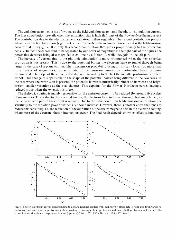
The emission current consists of two parts: the field-emission current and the photon-stimulation current.The first contribution prevails when the extraction bias is high (left part of the Fowler–Nordheim curves).The contribution due to the electromagnetic radiation is then negligible. The second contribution prevailswhen the extraction bias is low (right part of the Fowler–Nordheim curves), since then it is the field-emissioncurrent that is negligible. It is only this second contribution that grows proportionally to the power fluxdensity. In fact, the curves tend to be separated by one order of magnitude in the right part of the figures, thepower flux densities being also magnified each time by a factor 10, while they join in the left part.
The increase of current due to the photonic stimulation is more pronounced when the hemisphericalprotrusion is not present. This is due to the potential barrier the electrons have to tunnel through beinglarger in the case of a plane emitter. The transmission probability being intrinsically lower (by more thanthree orders of magnitude), the sensitivity of the emission current to photon-stimulation is morepronounced. The slope of the curve is also different according to the fact the metallic protrusion is presentor not. This change of slope is due to the shape of the potential barrier being different in the two cases. Inthe case where the protrusion is present, the potential barrier is intrinsically thinner so its width and heightpresent smaller variations as the bias changes. This explains for the Fowler–Nordheim curves having areduced slope when the extension is present.
The dielectric coating is mainly responsible for the emission current to be reduced (by around five ordersof magnitude). This is due to the potential barrier, the electrons have to tunnel through, becoming larger, sothe field-emission part of the current is reduced. Due to the reduction of this field-emission contribution, thesensitivity to the radiation power flux density should increase. However, there is another effect that tends toreduce this sensitivity, i.e. the reduction of the amplitude of the electromagnetic field in the dielectric coating,where most of the electron–photon interactions occur. The final result depends on which effect is dominant.
Fig. 3. Fowler–Nordheim curves corresponding to a plane tungsten emitter with, respectively, (from left to right and downwards) no
protrusion and no coating, a protrusion without coating, a coating without protrusion and finally both protrusion and coating. The
power flux densities in each representation are (upwards) 5.96� 1010, 5.96� 1011 and 5.96� 1012W/m2.
A. Mayer et al. / Ultramicroscopy 89 (2001) 95–104 101

In the case of a plane emitter, the potential barrier is intrinsically large, so the dielectric coating does notinduce a qualitative change of this feature. With the reduction of the electromagnetic field, there is finallyno significant change in sensitivity in this situation. However, in the case the protrusion is present, thepotential barrier is intrinsically thin so the dielectric coating does induce a qualitative change of this feature.Since the reduction of the field-emission contribution is much more important than in the previous case(with the relative increase the barrier width is larger), this effect is dominant and the sensitivity of theradiation power flux density is finally increased.
In both cases, it can be noted that the sensitivity to the radiation power flux density extends over a largerbias range. In fact in the left part of the Fowler–Nordheim figures, where the extraction bias is high, thepotential barrier is intrinsically thinner so the effect of the dielectric coating on this feature remainssignificant. The effects due to this increase of the potential barrier width tend to dominate those due to thereduction of the electromagnetic field, thus maintaining the sensitivity to the radiation power flux density.
The heating of the tip by the electromagnetic radiation was not considered. The change of temperatureinduced in the emitter by this heating depends on many parameters, including the time the radiation isapplied. In experimental conditions, the heating of the tip is controlled. Taking account of a giventemperature T in our model is, however, possible by considering the Fermi–Dirac distributionf(E, T)=1=½1þ eðE�Vstat�EFÞ=kT ] while integrating the current densities associated with the different energyvalues E. Growing (significantly), the temperature tends to increase the emission current (changing theheight and slope of the Fowler–Nordheim curves) and reduce the relative contribution of the photon-stimulated part of the current.
5. Experimental comparison
The first significant experimental work to fabricate and test control composite microemitters, consistingof a metal substrate of known microscopic profile and covered by a sub-micron layer of dielectric coating,was carried out by Latham and Mousa [26]. This was followed by a series of studies about a variety ofdielectric materials covering metallic micropoints [27–32]. They produced reversible current–voltage (I–V)characteristics that give a linear Fowler Nordheim (F–N) plot at low fields (o108V/m) and a saturatedemission at high fields (>4� 108V/m).
The results obtained were always compared with those of an uncoated emitter with approximately similartip radius. The data obtained from the composite emitters (a) demonstrate a displacement towards lowerenergies by around 0.7 eV with respect to the Fermi level (FL) of the metallic cathode; (b) have a larger full-width at half-maximum (FWHM) and (c) are more symmetrical than the core spectrum. The observedeffects, resulting mainly from carbon-based coatings, were identified in terms of a field-induced hot-electronemission (FIHEE) mechanism resulting from the field penetration in the insulating film, where conductingchannels are formed [33–35]. It was also possible to develop a technique to observe in situ and record theprocess of transition from cold to hot electron emission using polymeric layers of less than 20 nm thicknesson a field cathode metal tip. Recently, Forbes [36] introduced the most comprehensive review and analysisabout the origins of field induced electron emission from carbon based films and related materials.
The dielectric constant e=5 was the most agreeable value to be used in both experimental and theoreticalcalculations reported here [37]. The geometry used in Fig. 1 above is similar to the regime reportedexperimentally [26,34,38]. This is for field emission that is not photon stimulated. For comparison, the F–Nplots of an uncoated (curve A) and dielectric coated (curve B) are presented in Fig. 4 [26]. The high valuesof the emission current in curve B are related to the emission current switch-on process that is a feature ofthe thick dielectric coating, a process that does not happen in our simulations where a thinner dielectriccoating is considered. Konopsky et al. [38] reported a similar regime for coated Silicon tips with both field-and photo-assisted field emission study that produced similar results including the I–V characteristics and
A. Mayer et al. / Ultramicroscopy 89 (2001) 95–104102

F–N plots. The I–V characteristics of Fig. 3 is the most important and obvious feature of agreementbetween theoretical simulations and those obtained experimentally. The linearity of the I–V characteristicsobtained from clean uncoated tungsten emitters in both cases is noticeable. In addition, linearity of thecharacteristics at low fields and deviation from linearity at higher applied field values is also an observedfeature. The change of slope, which is due to the shape of the potential barrier being different in the twocases, is observed. Finally, the relation between the dielectric coating and the emission current is obtained inboth theoretical and experimental studies.
6. Conclusion
A stable and efficient technique, enabling the simulation of photon-stimulated field emission withconsideration of three-dimensional aspects, was presented. This technique was illustrated by a situationcharacterized with an axial symmetry, i.e. the electronic emission from a tungsten plane emitter thatsupports a 1-nm long hemispherical protrusion and a dielectric coating.
The Fowler–Nordheim curves were calculated, for various situations and various power flux densities. Itturns out that the sensitivity of the emission current to the power flux density of the electromagneticradiation is higher when the extraction bias is low and the emitter is a plane. These two factors tendindividually to reduce the field-emission part of the emission current, so achieving a good sensitivity to thispower-flux density while having enough basic current requires a compromise to be found. The dielectriccoating is responsible for the emission current to be reduced (by several orders of magnitude). According tothe conditions of this paper, it results in a larger sensitivity to the radiation power flux density only when aprotrusion is present. This sensitivity is extended to a larger bias range.
Fig. 4. Fowler–Nordheim plots of the uncoated (curve A) and dielectric coated (curve B) emitter.
A. Mayer et al. / Ultramicroscopy 89 (2001) 95–104 103

Acknowledgements
A.M. was supported as postdoctoral fellow by the Belgian National Fund for Scientific Research(FNRS). A.M. and J.-P.V. acknowledge the national program on the Interuniversity Research Project(PAI) and the use of the Namur Scientific Computing Facility, a common project between the FNRS, IBM-Belgium and the FUNDP. The authors are grateful to R.G. Forbes for useful discussions.
References
[1] E.R. Brown, K.A. McIntosh, K.B. Nichols, C.L. Dennis, Appl. Phys. Lett. 6 (1995) 285.
[2] C.A. Spindt, C.E. Holland, P.R. Schwoebel, I. Brodies, J. Vac. Sci. Technol. B 14 (1996) 1986.
[3] P.M. Phillips, R.E. Neidert, C. Hor, IEEE Trans. Electron Dev. 42 (1995) 1674.
[4] M.J. Hagmann, Ultramicroscopy 73 (1998) 89.
[5] M.J. Hagmann, Appl. Phys. Lett. 66 (1995) 79.
[6] M.J. Hagmann, J. Appl. Phys. 78 (1995) 25.
[7] M.J. Hagmann, Int. J. Quant. Chem. 70 (1998) 703.
[8] M.J. Hagmann, J. Vac. Sci. Technol B 14 (1996) 838.
[9] M.J. Hagmann, M. Brugat, J. Vac. Sci. Technol. B 15 (1997) 405.
[10] A. Mayer, J.-P. Vigneron, Phys. Rev. B 56 (19) (1997) 12599.
[11] A. Mayer, J.-P. Vigneron, J. Phys. 10 (4) (1998) 869.
[12] A. Mayer, J.-P. Vigneron, Phys. Rev. E 59 (4) (1999) 4659.
[13] A. Mayer, J.-P. Vigneron, Phys. Rev. B 60 (4) (1999) 2875.
[14] A. Mayer, J.-P. Vigneron, Phys. Rev. E 61 (5) (2000) 5953.
[15] A. Mayer, J.-P. Vigneron, Phys. Rev. E 60 (6) (1999) 7533.
[16] A. Mayer, J.-P. Vigneron, J. Vac. Sci. Technol. B 17 (2) (1999) 506.
[17] A. Mayer, J.-P. Vigneron, Ultramicroscopy 79 (1–4) (1999) 35.
[18] A. Mayer, P. Senet, J-P. Vigneron, J. Phys. 11 (44) (1999) 8617.
[19] V.T. Binh, V. Semet, N. Garcia, Ultramicroscopy 58 (1995) 307.
[20] A. Pimpale, S. Holloday, R.J. Smith, J. Phys. A 24 (1991) 3533.
[21] F.H.M. Faisal, Theory of Multiphoton Processes, Plenum, New York, 1987, pp. 8–10.
[22] T. Laloyaux, I. Derycke, J.P. Vigneron, P. Lambin, A.A. Lucas, Phys. Rev. B 47 (1993) 7508.
[23] J.B. Pendry, Low Energy Electron Diffraction, Academic Press, London, New York, 1974.
[24] R.H. Fowler, L. Nordheim, Proc. R. Soc. London, Ser. A 119 (1928) 173.
[25] R.H. Good, E. M .uller, Handb. Phys. 21 (1956) 176.
[26] R.V. Latham, M.S. Mousa, J. Phys. D 19 (1986) 699.
[27] M.S. Mousa, J. Phys. (Paris) 48 (C6) (1987) 109.
[28] M.S. Mousa, Vacuum 38 (1988) 835.
[29] M.S. Mousa, Surf. Sci. 231 (1990) 149.
[30] M.S. Mousa, Surf. Sci. 266 (1992) 110.
[31] M.S. Mousa, D.B. Hibbert, J. Phys. D 26 (1993) 697.
[32] M.S. Mousa, C.E. Holland, I. Brodie, C.A. Spindt, Appl. Surf. Sci. 67 (1993) 95.
[33] M.S. Mousa, K. Lorenz, N.S. Xu, Ultramicroscopy 79 (1999) 43.
[34] M.S. Mousa, J. Phys. (Paris) 48 (C6) (1987) 115.
[35] D.Z. Deng, Z.X. Yu, N.S. Xu, M.S. Mousa, R.V. Latham, Ultramicroscopy 79 (1999) 95.
[36] R.G. Forbes, Solid State Electron. 45 (6) (2001) 779.
[37] R.F. Forbes, Personal communication.
[38] V.N. Konopsky, V.V. Zhirnov, N.S. Sokolov, J.C. Alvarez, E.I. Givargizov, L.V. Bormatova, V.S. Letokhov, S.K. Sekatskii, J.
Phys. (Paris) 6 (C5) (1996) 129.
A. Mayer et al. / Ultramicroscopy 89 (2001) 95–104104